JP2011029636A - 銅柱バンプ上の金属間化合物の接合のための方法と構造 - Google Patents
銅柱バンプ上の金属間化合物の接合のための方法と構造 Download PDFInfo
- Publication number
- JP2011029636A JP2011029636A JP2010151626A JP2010151626A JP2011029636A JP 2011029636 A JP2011029636 A JP 2011029636A JP 2010151626 A JP2010151626 A JP 2010151626A JP 2010151626 A JP2010151626 A JP 2010151626A JP 2011029636 A JP2011029636 A JP 2011029636A
- Authority
- JP
- Japan
- Prior art keywords
- copper
- layer
- diffusion barrier
- barrier layer
- intermetallic compound
- Prior art date
- Legal status (The legal status is an assumption and is not a legal conclusion. Google has not performed a legal analysis and makes no representation as to the accuracy of the status listed.)
- Pending
Links
Images


Classifications
-
- H—ELECTRICITY
- H01—ELECTRIC ELEMENTS
- H01L—SEMICONDUCTOR DEVICES NOT COVERED BY CLASS H10
- H01L23/00—Details of semiconductor or other solid state devices
- H01L23/48—Arrangements for conducting electric current to or from the solid state body in operation, e.g. leads, terminal arrangements ; Selection of materials therefor
- H01L23/488—Arrangements for conducting electric current to or from the solid state body in operation, e.g. leads, terminal arrangements ; Selection of materials therefor consisting of soldered or bonded constructions
- H01L23/498—Leads, i.e. metallisations or lead-frames on insulating substrates, e.g. chip carriers
- H01L23/49811—Additional leads joined to the metallisation on the insulating substrate, e.g. pins, bumps, wires, flat leads
- H01L23/49816—Spherical bumps on the substrate for external connection, e.g. ball grid arrays [BGA]
-
- H—ELECTRICITY
- H01—ELECTRIC ELEMENTS
- H01L—SEMICONDUCTOR DEVICES NOT COVERED BY CLASS H10
- H01L24/00—Arrangements for connecting or disconnecting semiconductor or solid-state bodies; Methods or apparatus related thereto
- H01L24/01—Means for bonding being attached to, or being formed on, the surface to be connected, e.g. chip-to-package, die-attach, "first-level" interconnects; Manufacturing methods related thereto
- H01L24/10—Bump connectors ; Manufacturing methods related thereto
- H01L24/11—Manufacturing methods
-
- H—ELECTRICITY
- H01—ELECTRIC ELEMENTS
- H01L—SEMICONDUCTOR DEVICES NOT COVERED BY CLASS H10
- H01L24/00—Arrangements for connecting or disconnecting semiconductor or solid-state bodies; Methods or apparatus related thereto
- H01L24/01—Means for bonding being attached to, or being formed on, the surface to be connected, e.g. chip-to-package, die-attach, "first-level" interconnects; Manufacturing methods related thereto
- H01L24/10—Bump connectors ; Manufacturing methods related thereto
- H01L24/12—Structure, shape, material or disposition of the bump connectors prior to the connecting process
- H01L24/13—Structure, shape, material or disposition of the bump connectors prior to the connecting process of an individual bump connector
-
- H—ELECTRICITY
- H01—ELECTRIC ELEMENTS
- H01L—SEMICONDUCTOR DEVICES NOT COVERED BY CLASS H10
- H01L24/00—Arrangements for connecting or disconnecting semiconductor or solid-state bodies; Methods or apparatus related thereto
- H01L24/01—Means for bonding being attached to, or being formed on, the surface to be connected, e.g. chip-to-package, die-attach, "first-level" interconnects; Manufacturing methods related thereto
- H01L24/10—Bump connectors ; Manufacturing methods related thereto
- H01L24/15—Structure, shape, material or disposition of the bump connectors after the connecting process
- H01L24/16—Structure, shape, material or disposition of the bump connectors after the connecting process of an individual bump connector
-
- H—ELECTRICITY
- H01—ELECTRIC ELEMENTS
- H01L—SEMICONDUCTOR DEVICES NOT COVERED BY CLASS H10
- H01L24/00—Arrangements for connecting or disconnecting semiconductor or solid-state bodies; Methods or apparatus related thereto
- H01L24/80—Methods for connecting semiconductor or other solid state bodies using means for bonding being attached to, or being formed on, the surface to be connected
- H01L24/81—Methods for connecting semiconductor or other solid state bodies using means for bonding being attached to, or being formed on, the surface to be connected using a bump connector
-
- H—ELECTRICITY
- H01—ELECTRIC ELEMENTS
- H01L—SEMICONDUCTOR DEVICES NOT COVERED BY CLASS H10
- H01L2224/00—Indexing scheme for arrangements for connecting or disconnecting semiconductor or solid-state bodies and methods related thereto as covered by H01L24/00
- H01L2224/01—Means for bonding being attached to, or being formed on, the surface to be connected, e.g. chip-to-package, die-attach, "first-level" interconnects; Manufacturing methods related thereto
- H01L2224/10—Bump connectors; Manufacturing methods related thereto
- H01L2224/11—Manufacturing methods
- H01L2224/114—Manufacturing methods by blanket deposition of the material of the bump connector
- H01L2224/1146—Plating
- H01L2224/11462—Electroplating
-
- H—ELECTRICITY
- H01—ELECTRIC ELEMENTS
- H01L—SEMICONDUCTOR DEVICES NOT COVERED BY CLASS H10
- H01L2224/00—Indexing scheme for arrangements for connecting or disconnecting semiconductor or solid-state bodies and methods related thereto as covered by H01L24/00
- H01L2224/01—Means for bonding being attached to, or being formed on, the surface to be connected, e.g. chip-to-package, die-attach, "first-level" interconnects; Manufacturing methods related thereto
- H01L2224/10—Bump connectors; Manufacturing methods related thereto
- H01L2224/11—Manufacturing methods
- H01L2224/1147—Manufacturing methods using a lift-off mask
-
- H—ELECTRICITY
- H01—ELECTRIC ELEMENTS
- H01L—SEMICONDUCTOR DEVICES NOT COVERED BY CLASS H10
- H01L2224/00—Indexing scheme for arrangements for connecting or disconnecting semiconductor or solid-state bodies and methods related thereto as covered by H01L24/00
- H01L2224/01—Means for bonding being attached to, or being formed on, the surface to be connected, e.g. chip-to-package, die-attach, "first-level" interconnects; Manufacturing methods related thereto
- H01L2224/10—Bump connectors; Manufacturing methods related thereto
- H01L2224/11—Manufacturing methods
- H01L2224/119—Methods of manufacturing bump connectors involving a specific sequence of method steps
- H01L2224/11901—Methods of manufacturing bump connectors involving a specific sequence of method steps with repetition of the same manufacturing step
-
- H—ELECTRICITY
- H01—ELECTRIC ELEMENTS
- H01L—SEMICONDUCTOR DEVICES NOT COVERED BY CLASS H10
- H01L2224/00—Indexing scheme for arrangements for connecting or disconnecting semiconductor or solid-state bodies and methods related thereto as covered by H01L24/00
- H01L2224/01—Means for bonding being attached to, or being formed on, the surface to be connected, e.g. chip-to-package, die-attach, "first-level" interconnects; Manufacturing methods related thereto
- H01L2224/10—Bump connectors; Manufacturing methods related thereto
- H01L2224/12—Structure, shape, material or disposition of the bump connectors prior to the connecting process
- H01L2224/13—Structure, shape, material or disposition of the bump connectors prior to the connecting process of an individual bump connector
- H01L2224/13001—Core members of the bump connector
- H01L2224/13075—Plural core members
- H01L2224/1308—Plural core members being stacked
- H01L2224/13084—Four-layer arrangements
-
- H—ELECTRICITY
- H01—ELECTRIC ELEMENTS
- H01L—SEMICONDUCTOR DEVICES NOT COVERED BY CLASS H10
- H01L2224/00—Indexing scheme for arrangements for connecting or disconnecting semiconductor or solid-state bodies and methods related thereto as covered by H01L24/00
- H01L2224/01—Means for bonding being attached to, or being formed on, the surface to be connected, e.g. chip-to-package, die-attach, "first-level" interconnects; Manufacturing methods related thereto
- H01L2224/10—Bump connectors; Manufacturing methods related thereto
- H01L2224/12—Structure, shape, material or disposition of the bump connectors prior to the connecting process
- H01L2224/13—Structure, shape, material or disposition of the bump connectors prior to the connecting process of an individual bump connector
- H01L2224/13001—Core members of the bump connector
- H01L2224/13099—Material
- H01L2224/131—Material with a principal constituent of the material being a metal or a metalloid, e.g. boron [B], silicon [Si], germanium [Ge], arsenic [As], antimony [Sb], tellurium [Te] and polonium [Po], and alloys thereof
- H01L2224/13138—Material with a principal constituent of the material being a metal or a metalloid, e.g. boron [B], silicon [Si], germanium [Ge], arsenic [As], antimony [Sb], tellurium [Te] and polonium [Po], and alloys thereof the principal constituent melting at a temperature of greater than or equal to 950°C and less than 1550°C
- H01L2224/13147—Copper [Cu] as principal constituent
-
- H—ELECTRICITY
- H01—ELECTRIC ELEMENTS
- H01L—SEMICONDUCTOR DEVICES NOT COVERED BY CLASS H10
- H01L2224/00—Indexing scheme for arrangements for connecting or disconnecting semiconductor or solid-state bodies and methods related thereto as covered by H01L24/00
- H01L2224/01—Means for bonding being attached to, or being formed on, the surface to be connected, e.g. chip-to-package, die-attach, "first-level" interconnects; Manufacturing methods related thereto
- H01L2224/10—Bump connectors; Manufacturing methods related thereto
- H01L2224/12—Structure, shape, material or disposition of the bump connectors prior to the connecting process
- H01L2224/13—Structure, shape, material or disposition of the bump connectors prior to the connecting process of an individual bump connector
- H01L2224/1354—Coating
- H01L2224/13575—Plural coating layers
- H01L2224/1358—Plural coating layers being stacked
- H01L2224/13583—Three-layer coating
-
- H—ELECTRICITY
- H01—ELECTRIC ELEMENTS
- H01L—SEMICONDUCTOR DEVICES NOT COVERED BY CLASS H10
- H01L2224/00—Indexing scheme for arrangements for connecting or disconnecting semiconductor or solid-state bodies and methods related thereto as covered by H01L24/00
- H01L2224/01—Means for bonding being attached to, or being formed on, the surface to be connected, e.g. chip-to-package, die-attach, "first-level" interconnects; Manufacturing methods related thereto
- H01L2224/10—Bump connectors; Manufacturing methods related thereto
- H01L2224/12—Structure, shape, material or disposition of the bump connectors prior to the connecting process
- H01L2224/13—Structure, shape, material or disposition of the bump connectors prior to the connecting process of an individual bump connector
- H01L2224/1354—Coating
- H01L2224/13599—Material
- H01L2224/136—Material with a principal constituent of the material being a metal or a metalloid, e.g. boron [B], silicon [Si], germanium [Ge], arsenic [As], antimony [Sb], tellurium [Te] and polonium [Po], and alloys thereof
- H01L2224/13601—Material with a principal constituent of the material being a metal or a metalloid, e.g. boron [B], silicon [Si], germanium [Ge], arsenic [As], antimony [Sb], tellurium [Te] and polonium [Po], and alloys thereof the principal constituent melting at a temperature of less than 400°C
- H01L2224/13611—Tin [Sn] as principal constituent
-
- H—ELECTRICITY
- H01—ELECTRIC ELEMENTS
- H01L—SEMICONDUCTOR DEVICES NOT COVERED BY CLASS H10
- H01L2224/00—Indexing scheme for arrangements for connecting or disconnecting semiconductor or solid-state bodies and methods related thereto as covered by H01L24/00
- H01L2224/01—Means for bonding being attached to, or being formed on, the surface to be connected, e.g. chip-to-package, die-attach, "first-level" interconnects; Manufacturing methods related thereto
- H01L2224/10—Bump connectors; Manufacturing methods related thereto
- H01L2224/12—Structure, shape, material or disposition of the bump connectors prior to the connecting process
- H01L2224/13—Structure, shape, material or disposition of the bump connectors prior to the connecting process of an individual bump connector
- H01L2224/1354—Coating
- H01L2224/13599—Material
- H01L2224/136—Material with a principal constituent of the material being a metal or a metalloid, e.g. boron [B], silicon [Si], germanium [Ge], arsenic [As], antimony [Sb], tellurium [Te] and polonium [Po], and alloys thereof
- H01L2224/13638—Material with a principal constituent of the material being a metal or a metalloid, e.g. boron [B], silicon [Si], germanium [Ge], arsenic [As], antimony [Sb], tellurium [Te] and polonium [Po], and alloys thereof the principal constituent melting at a temperature of greater than or equal to 950°C and less than 1550°C
- H01L2224/13655—Nickel [Ni] as principal constituent
-
- H—ELECTRICITY
- H01—ELECTRIC ELEMENTS
- H01L—SEMICONDUCTOR DEVICES NOT COVERED BY CLASS H10
- H01L2224/00—Indexing scheme for arrangements for connecting or disconnecting semiconductor or solid-state bodies and methods related thereto as covered by H01L24/00
- H01L2224/01—Means for bonding being attached to, or being formed on, the surface to be connected, e.g. chip-to-package, die-attach, "first-level" interconnects; Manufacturing methods related thereto
- H01L2224/10—Bump connectors; Manufacturing methods related thereto
- H01L2224/15—Structure, shape, material or disposition of the bump connectors after the connecting process
- H01L2224/16—Structure, shape, material or disposition of the bump connectors after the connecting process of an individual bump connector
-
- H—ELECTRICITY
- H01—ELECTRIC ELEMENTS
- H01L—SEMICONDUCTOR DEVICES NOT COVERED BY CLASS H10
- H01L2224/00—Indexing scheme for arrangements for connecting or disconnecting semiconductor or solid-state bodies and methods related thereto as covered by H01L24/00
- H01L2224/80—Methods for connecting semiconductor or other solid state bodies using means for bonding being attached to, or being formed on, the surface to be connected
- H01L2224/81—Methods for connecting semiconductor or other solid state bodies using means for bonding being attached to, or being formed on, the surface to be connected using a bump connector
- H01L2224/8119—Arrangement of the bump connectors prior to mounting
- H01L2224/81191—Arrangement of the bump connectors prior to mounting wherein the bump connectors are disposed only on the semiconductor or solid-state body
-
- H—ELECTRICITY
- H01—ELECTRIC ELEMENTS
- H01L—SEMICONDUCTOR DEVICES NOT COVERED BY CLASS H10
- H01L2224/00—Indexing scheme for arrangements for connecting or disconnecting semiconductor or solid-state bodies and methods related thereto as covered by H01L24/00
- H01L2224/80—Methods for connecting semiconductor or other solid state bodies using means for bonding being attached to, or being formed on, the surface to be connected
- H01L2224/81—Methods for connecting semiconductor or other solid state bodies using means for bonding being attached to, or being formed on, the surface to be connected using a bump connector
- H01L2224/8119—Arrangement of the bump connectors prior to mounting
- H01L2224/81193—Arrangement of the bump connectors prior to mounting wherein the bump connectors are disposed on both the semiconductor or solid-state body and another item or body to be connected to the semiconductor or solid-state body
-
- H—ELECTRICITY
- H01—ELECTRIC ELEMENTS
- H01L—SEMICONDUCTOR DEVICES NOT COVERED BY CLASS H10
- H01L2224/00—Indexing scheme for arrangements for connecting or disconnecting semiconductor or solid-state bodies and methods related thereto as covered by H01L24/00
- H01L2224/80—Methods for connecting semiconductor or other solid state bodies using means for bonding being attached to, or being formed on, the surface to be connected
- H01L2224/81—Methods for connecting semiconductor or other solid state bodies using means for bonding being attached to, or being formed on, the surface to be connected using a bump connector
- H01L2224/818—Bonding techniques
- H01L2224/81801—Soldering or alloying
-
- H—ELECTRICITY
- H01—ELECTRIC ELEMENTS
- H01L—SEMICONDUCTOR DEVICES NOT COVERED BY CLASS H10
- H01L2924/00—Indexing scheme for arrangements or methods for connecting or disconnecting semiconductor or solid-state bodies as covered by H01L24/00
- H01L2924/0001—Technical content checked by a classifier
- H01L2924/00013—Fully indexed content
-
- H—ELECTRICITY
- H01—ELECTRIC ELEMENTS
- H01L—SEMICONDUCTOR DEVICES NOT COVERED BY CLASS H10
- H01L2924/00—Indexing scheme for arrangements or methods for connecting or disconnecting semiconductor or solid-state bodies as covered by H01L24/00
- H01L2924/01—Chemical elements
- H01L2924/01006—Carbon [C]
-
- H—ELECTRICITY
- H01—ELECTRIC ELEMENTS
- H01L—SEMICONDUCTOR DEVICES NOT COVERED BY CLASS H10
- H01L2924/00—Indexing scheme for arrangements or methods for connecting or disconnecting semiconductor or solid-state bodies as covered by H01L24/00
- H01L2924/01—Chemical elements
- H01L2924/01013—Aluminum [Al]
-
- H—ELECTRICITY
- H01—ELECTRIC ELEMENTS
- H01L—SEMICONDUCTOR DEVICES NOT COVERED BY CLASS H10
- H01L2924/00—Indexing scheme for arrangements or methods for connecting or disconnecting semiconductor or solid-state bodies as covered by H01L24/00
- H01L2924/01—Chemical elements
- H01L2924/01019—Potassium [K]
-
- H—ELECTRICITY
- H01—ELECTRIC ELEMENTS
- H01L—SEMICONDUCTOR DEVICES NOT COVERED BY CLASS H10
- H01L2924/00—Indexing scheme for arrangements or methods for connecting or disconnecting semiconductor or solid-state bodies as covered by H01L24/00
- H01L2924/01—Chemical elements
- H01L2924/01022—Titanium [Ti]
-
- H—ELECTRICITY
- H01—ELECTRIC ELEMENTS
- H01L—SEMICONDUCTOR DEVICES NOT COVERED BY CLASS H10
- H01L2924/00—Indexing scheme for arrangements or methods for connecting or disconnecting semiconductor or solid-state bodies as covered by H01L24/00
- H01L2924/01—Chemical elements
- H01L2924/01023—Vanadium [V]
-
- H—ELECTRICITY
- H01—ELECTRIC ELEMENTS
- H01L—SEMICONDUCTOR DEVICES NOT COVERED BY CLASS H10
- H01L2924/00—Indexing scheme for arrangements or methods for connecting or disconnecting semiconductor or solid-state bodies as covered by H01L24/00
- H01L2924/01—Chemical elements
- H01L2924/01029—Copper [Cu]
-
- H—ELECTRICITY
- H01—ELECTRIC ELEMENTS
- H01L—SEMICONDUCTOR DEVICES NOT COVERED BY CLASS H10
- H01L2924/00—Indexing scheme for arrangements or methods for connecting or disconnecting semiconductor or solid-state bodies as covered by H01L24/00
- H01L2924/01—Chemical elements
- H01L2924/0103—Zinc [Zn]
-
- H—ELECTRICITY
- H01—ELECTRIC ELEMENTS
- H01L—SEMICONDUCTOR DEVICES NOT COVERED BY CLASS H10
- H01L2924/00—Indexing scheme for arrangements or methods for connecting or disconnecting semiconductor or solid-state bodies as covered by H01L24/00
- H01L2924/01—Chemical elements
- H01L2924/01033—Arsenic [As]
-
- H—ELECTRICITY
- H01—ELECTRIC ELEMENTS
- H01L—SEMICONDUCTOR DEVICES NOT COVERED BY CLASS H10
- H01L2924/00—Indexing scheme for arrangements or methods for connecting or disconnecting semiconductor or solid-state bodies as covered by H01L24/00
- H01L2924/01—Chemical elements
- H01L2924/01047—Silver [Ag]
-
- H—ELECTRICITY
- H01—ELECTRIC ELEMENTS
- H01L—SEMICONDUCTOR DEVICES NOT COVERED BY CLASS H10
- H01L2924/00—Indexing scheme for arrangements or methods for connecting or disconnecting semiconductor or solid-state bodies as covered by H01L24/00
- H01L2924/01—Chemical elements
- H01L2924/01049—Indium [In]
-
- H—ELECTRICITY
- H01—ELECTRIC ELEMENTS
- H01L—SEMICONDUCTOR DEVICES NOT COVERED BY CLASS H10
- H01L2924/00—Indexing scheme for arrangements or methods for connecting or disconnecting semiconductor or solid-state bodies as covered by H01L24/00
- H01L2924/01—Chemical elements
- H01L2924/0105—Tin [Sn]
-
- H—ELECTRICITY
- H01—ELECTRIC ELEMENTS
- H01L—SEMICONDUCTOR DEVICES NOT COVERED BY CLASS H10
- H01L2924/00—Indexing scheme for arrangements or methods for connecting or disconnecting semiconductor or solid-state bodies as covered by H01L24/00
- H01L2924/01—Chemical elements
- H01L2924/01074—Tungsten [W]
-
- H—ELECTRICITY
- H01—ELECTRIC ELEMENTS
- H01L—SEMICONDUCTOR DEVICES NOT COVERED BY CLASS H10
- H01L2924/00—Indexing scheme for arrangements or methods for connecting or disconnecting semiconductor or solid-state bodies as covered by H01L24/00
- H01L2924/01—Chemical elements
- H01L2924/01075—Rhenium [Re]
-
- H—ELECTRICITY
- H01—ELECTRIC ELEMENTS
- H01L—SEMICONDUCTOR DEVICES NOT COVERED BY CLASS H10
- H01L2924/00—Indexing scheme for arrangements or methods for connecting or disconnecting semiconductor or solid-state bodies as covered by H01L24/00
- H01L2924/01—Chemical elements
- H01L2924/01078—Platinum [Pt]
-
- H—ELECTRICITY
- H01—ELECTRIC ELEMENTS
- H01L—SEMICONDUCTOR DEVICES NOT COVERED BY CLASS H10
- H01L2924/00—Indexing scheme for arrangements or methods for connecting or disconnecting semiconductor or solid-state bodies as covered by H01L24/00
- H01L2924/01—Chemical elements
- H01L2924/01079—Gold [Au]
-
- H—ELECTRICITY
- H01—ELECTRIC ELEMENTS
- H01L—SEMICONDUCTOR DEVICES NOT COVERED BY CLASS H10
- H01L2924/00—Indexing scheme for arrangements or methods for connecting or disconnecting semiconductor or solid-state bodies as covered by H01L24/00
- H01L2924/01—Chemical elements
- H01L2924/01082—Lead [Pb]
-
- H—ELECTRICITY
- H01—ELECTRIC ELEMENTS
- H01L—SEMICONDUCTOR DEVICES NOT COVERED BY CLASS H10
- H01L2924/00—Indexing scheme for arrangements or methods for connecting or disconnecting semiconductor or solid-state bodies as covered by H01L24/00
- H01L2924/013—Alloys
- H01L2924/0132—Binary Alloys
- H01L2924/01327—Intermediate phases, i.e. intermetallics compounds
-
- H—ELECTRICITY
- H01—ELECTRIC ELEMENTS
- H01L—SEMICONDUCTOR DEVICES NOT COVERED BY CLASS H10
- H01L2924/00—Indexing scheme for arrangements or methods for connecting or disconnecting semiconductor or solid-state bodies as covered by H01L24/00
- H01L2924/013—Alloys
- H01L2924/014—Solder alloys
-
- H—ELECTRICITY
- H01—ELECTRIC ELEMENTS
- H01L—SEMICONDUCTOR DEVICES NOT COVERED BY CLASS H10
- H01L2924/00—Indexing scheme for arrangements or methods for connecting or disconnecting semiconductor or solid-state bodies as covered by H01L24/00
- H01L2924/10—Details of semiconductor or other solid state devices to be connected
- H01L2924/11—Device type
- H01L2924/14—Integrated circuits
-
- H—ELECTRICITY
- H01—ELECTRIC ELEMENTS
- H01L—SEMICONDUCTOR DEVICES NOT COVERED BY CLASS H10
- H01L2924/00—Indexing scheme for arrangements or methods for connecting or disconnecting semiconductor or solid-state bodies as covered by H01L24/00
- H01L2924/10—Details of semiconductor or other solid state devices to be connected
- H01L2924/146—Mixed devices
- H01L2924/1461—MEMS
-
- Y—GENERAL TAGGING OF NEW TECHNOLOGICAL DEVELOPMENTS; GENERAL TAGGING OF CROSS-SECTIONAL TECHNOLOGIES SPANNING OVER SEVERAL SECTIONS OF THE IPC; TECHNICAL SUBJECTS COVERED BY FORMER USPC CROSS-REFERENCE ART COLLECTIONS [XRACs] AND DIGESTS
- Y10—TECHNICAL SUBJECTS COVERED BY FORMER USPC
- Y10T—TECHNICAL SUBJECTS COVERED BY FORMER US CLASSIFICATION
- Y10T428/00—Stock material or miscellaneous articles
- Y10T428/24—Structurally defined web or sheet [e.g., overall dimension, etc.]
- Y10T428/24479—Structurally defined web or sheet [e.g., overall dimension, etc.] including variation in thickness
- Y10T428/24612—Composite web or sheet
Abstract
【解決手段】銅柱108層を形成するために銅を堆積するステップと、銅柱層の上部に拡散バリア層110を堆積するステップと、拡散バリア層上に銅キャップ層112を形成するステップを含み、金属間化合物116(IMC)が拡散バリア層、銅キャップ層、銅キャップ層上に形成されたはんだ層の間に形成される。IMCは銅柱構造上で良好な接合性を有し、IMCの厚さは銅キャップ層の厚さで制御することができ、拡散バリア層は銅柱層からはんだ層への銅の拡散を抑制する。銅キャップ層を形成する前に、拡散バリア層上部の濡れ性のために薄膜層を堆積するステップを更に含むことができる。
【選択図】図1
Description
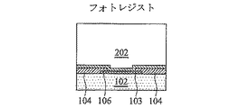
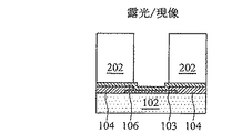
103 金属線層
104 保護層
106 シード層
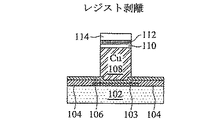
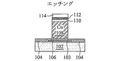
108 銅柱
110 拡散バリア層
112 銅キャップ層
114 はんだ層
116 金属間化合物層
202 フォトレジスト層
204 プリント回路板(PCB)
206 導電層
208 拡散バリア層
210 金属間化合物層
Claims (19)
- 銅含有柱層を形成するステップ、
前記銅含有柱層上に拡散バリア層を堆積するステップ、及び
前記拡散バリア層上に金属間化合物(IMC)を形成するステップを含む、柱構造を形成する方法。 - 前記金属間化合物の形成は、
前記拡散バリア層上に銅含有キャップ層を堆積するステップ、
前記銅含有キャップ層上にはんだ層を堆積するステップ、及び
前記金属間化合物を形成するために前記銅含有キャップ層と前記はんだ層を熱処理するステップを含む請求項1に記載の方法。 - 前記金属間化合物の厚さを決定するために前記銅含有キャップ層の厚さを制御するステップを更に含む請求項2に記載の方法。
- 前記銅含有キャップ層は0.1μm〜1.5μmの厚さに堆積される請求項2に記載の方法。
- 前記金属間化合物を形成する熱処理は、最大の厚さが7μmを有する銅−ニッケル−スズで作られる請求項2に記載の方法。
- 前記金属間化合物を形成する前に前記拡散バリア層の上部に約0.01μm〜0.1μmの厚さで金を堆積するステップを更に含む請求項1に記載の方法。
- 前記拡散バリア層は、ニッケル、ニッケルリンNi(P)、ニッケルバナジウムNi(V)、またはそれらの組み合わせを含む請求項1に記載の方法。
- 前記拡散バリア層は0.5μm〜4μmの厚さに堆積される請求項1に記載の方法。
- 前記銅含有柱層は30μm〜150μmの厚さに堆積される請求項1に記載の方法。
- 銅含有柱層、
前記銅含有柱層上の拡散バリア層、
前記拡散バリア層上の金属間化合物(IMC)、及び
前記金属間化合物上のはんだ層を含む柱構造。 - 前記拡散バリア層は、ニッケル、ニッケルリンNi(P)、ニッケルバナジウムNi(V)、またはそれらの組み合わせを含む請求項10に記載の構造。
- 前記拡散バリア層は0.5μm〜4μmの厚さを持つ請求項10に記載の構造。
- 前記銅含有柱層は30μm〜150μmの厚さを持つ請求項10に記載の構造。
- 前記金属間化合物は、最大の厚さが7μmを有する銅−ニッケル−スズを含む請求項10に記載の構造。
- プリント回路板、及び
前記プリント回路板とフリップチップ接合され、柱構造を有する半導体ウエハを含み、前記柱構造は、
銅含有柱層、
前記銅含有柱層上の拡散バリア層、
前記拡散バリア層上の金属間化合物(IMC)、及び
前記プリント回路板とフリップチップ接合するはんだ層を含むフリップチップボンディング構造。 - 前記拡散バリア層は、ニッケル、ニッケルリンNi(P)、ニッケルバナジウムNi(V)、またはそれらの組み合わせを含む請求項15に記載のフリップチップボンディング構造。
- 前記拡散バリア層は0.5μm〜4μmの厚さを持つ請求項15に記載のフリップチップボンディング構造。
- 前記銅含有柱層は30μm〜150μmの厚さを持つ請求項15に記載のフリップチップボンディング構造。
- 前記金属間化合物は、最大の厚さが7μmを有する銅−ニッケル−スズを含む請求項15に記載のフリップチップボンディング構造。
Applications Claiming Priority (2)
| Application Number | Priority Date | Filing Date | Title |
|---|---|---|---|
| US22286009P | 2009-07-02 | 2009-07-02 | |
| US12/825,822 US8592995B2 (en) | 2009-07-02 | 2010-06-29 | Method and structure for adhesion of intermetallic compound (IMC) on Cu pillar bump |
Related Child Applications (1)
| Application Number | Title | Priority Date | Filing Date |
|---|---|---|---|
| JP2013076744A Division JP5756140B2 (ja) | 2009-07-02 | 2013-04-02 | 銅柱バンプ上の金属間化合物の接合のための方法 |
Publications (2)
| Publication Number | Publication Date |
|---|---|
| JP2011029636A true JP2011029636A (ja) | 2011-02-10 |
| JP2011029636A5 JP2011029636A5 (ja) | 2012-07-05 |
Family
ID=43412194
Family Applications (3)
| Application Number | Title | Priority Date | Filing Date |
|---|---|---|---|
| JP2010151626A Pending JP2011029636A (ja) | 2009-07-02 | 2010-07-02 | 銅柱バンプ上の金属間化合物の接合のための方法と構造 |
| JP2013076744A Active JP5756140B2 (ja) | 2009-07-02 | 2013-04-02 | 銅柱バンプ上の金属間化合物の接合のための方法 |
| JP2015031242A Active JP6352205B2 (ja) | 2009-07-02 | 2015-02-20 | 銅柱バンプ上の金属間化合物の接合のための構造 |
Family Applications After (2)
| Application Number | Title | Priority Date | Filing Date |
|---|---|---|---|
| JP2013076744A Active JP5756140B2 (ja) | 2009-07-02 | 2013-04-02 | 銅柱バンプ上の金属間化合物の接合のための方法 |
| JP2015031242A Active JP6352205B2 (ja) | 2009-07-02 | 2015-02-20 | 銅柱バンプ上の金属間化合物の接合のための構造 |
Country Status (5)
| Country | Link |
|---|---|
| US (1) | US8592995B2 (ja) |
| JP (3) | JP2011029636A (ja) |
| KR (1) | KR101344553B1 (ja) |
| CN (1) | CN101944496B (ja) |
| TW (1) | TWI498981B (ja) |
Cited By (13)
| Publication number | Priority date | Publication date | Assignee | Title |
|---|---|---|---|---|
| JP2012222191A (ja) * | 2011-04-11 | 2012-11-12 | Okuno Chem Ind Co Ltd | Led照明ユニット |
| JP2013135014A (ja) * | 2011-12-26 | 2013-07-08 | Fujitsu Ltd | 電子部品及び電子機器 |
| JP2013211511A (ja) * | 2012-02-29 | 2013-10-10 | Renesas Electronics Corp | 半導体装置及び半導体装置の製造方法 |
| JP2014090001A (ja) * | 2012-10-29 | 2014-05-15 | Fujitsu Ltd | 電子部品、電子部品の製造方法及び電子装置の製造方法 |
| JP2014116367A (ja) * | 2012-12-06 | 2014-06-26 | Fujitsu Ltd | 電子部品、電子装置の製造方法及び電子装置 |
| JP2015213103A (ja) * | 2014-05-01 | 2015-11-26 | 三菱電機株式会社 | 半導体装置およびその実装構造 |
| JP2016032090A (ja) * | 2014-07-25 | 2016-03-07 | ▲き▼邦科技股▲分▼有限公司 | 基板及びその製造方法 |
| KR20170033393A (ko) | 2014-08-29 | 2017-03-24 | 닛데쓰스미킹 마이크로 메탈 가부시키가이샤 | 반도체 접속의 Cu 필러용 원기둥상 형성물 |
| JP2018166224A (ja) * | 2016-12-23 | 2018-10-25 | ルーメンス カンパニー リミテッド | マイクロledモジュール及びその製造方法 |
| KR20210023811A (ko) | 2018-06-27 | 2021-03-04 | 디아이씨 가부시끼가이샤 | 필러 형성용 도전 페이스트 |
| KR20210035187A (ko) | 2018-07-26 | 2021-03-31 | 디아이씨 가부시끼가이샤 | 도전성 페이스트를 이용한 도전성 필러의 제조 방법 |
| KR20210047885A (ko) | 2018-08-24 | 2021-04-30 | 제이에스알 가부시끼가이샤 | 감광 수지 조성물, 레지스트 패턴의 형성 방법, 도금 조형물의 제조 방법 및 반도체 장치 |
| CN114367730A (zh) * | 2021-12-16 | 2022-04-19 | 武汉大学 | 基于金刚石间接拉伸结构的金刚石/块铜衬底扩散键合工艺及结构 |
Families Citing this family (64)
| Publication number | Priority date | Publication date | Assignee | Title |
|---|---|---|---|---|
| TWI245402B (en) * | 2002-01-07 | 2005-12-11 | Megic Corp | Rod soldering structure and manufacturing process thereof |
| TWI584434B (zh) * | 2010-04-20 | 2017-05-21 | 瑞鼎科技股份有限公司 | 晶粒結構及晶粒接合方法 |
| US9142533B2 (en) | 2010-05-20 | 2015-09-22 | Taiwan Semiconductor Manufacturing Company, Ltd. | Substrate interconnections having different sizes |
| US8581420B2 (en) * | 2010-10-18 | 2013-11-12 | Taiwan Semiconductor Manufacturing Company, Ltd. | Under-bump metallization (UBM) structure and method of forming the same |
| US20120313234A1 (en) * | 2011-06-10 | 2012-12-13 | Geng-Shin Shen | Qfn package and manufacturing process thereof |
| US10833033B2 (en) * | 2011-07-27 | 2020-11-10 | Taiwan Semiconductor Manufacturing Co., Ltd. | Bump structure having a side recess and semiconductor structure including the same |
| US8643196B2 (en) * | 2011-07-27 | 2014-02-04 | Taiwan Semiconductor Manufacturing Company, Ltd. | Structure and method for bump to landing trace ratio |
| EP2565297A3 (en) | 2011-08-30 | 2013-04-24 | Rohm and Haas Electronic Materials LLC | Adhesion promotion of cyanide-free white bronze |
| US9219016B2 (en) * | 2011-09-28 | 2015-12-22 | Taiwan Semiconductor Manufacturing Company, Ltd. | Structure design for 3DIC testing |
| KR101301795B1 (ko) * | 2011-10-04 | 2013-08-29 | 앰코 테크놀로지 코리아 주식회사 | 반도체 패키지 |
| US9786622B2 (en) * | 2011-10-20 | 2017-10-10 | Taiwan Semiconductor Manufacturing Company, Ltd. | Semiconductor package |
| KR101359733B1 (ko) * | 2011-12-16 | 2014-02-11 | 성균관대학교산학협력단 | 반도체 3차원 적층공정에서의 이중 확산방지층을 포함하는 범프 및 그 제조방법 |
| CN102437135A (zh) * | 2011-12-19 | 2012-05-02 | 南通富士通微电子股份有限公司 | 圆片级柱状凸点封装结构 |
| CN102496606B (zh) * | 2011-12-19 | 2014-11-12 | 南通富士通微电子股份有限公司 | 一种高可靠圆片级柱状凸点封装结构 |
| CN102496584A (zh) * | 2011-12-19 | 2012-06-13 | 南通富士通微电子股份有限公司 | 一种焊料凸点的形成方法 |
| CN102496605B (zh) * | 2011-12-19 | 2014-11-12 | 南通富士通微电子股份有限公司 | 一种圆片级封装结构 |
| CN102496585A (zh) * | 2011-12-19 | 2012-06-13 | 南通富士通微电子股份有限公司 | 一种新型圆片级封装方法 |
| TWI467718B (zh) * | 2011-12-30 | 2015-01-01 | Ind Tech Res Inst | 凸塊結構以及電子封裝接點結構及其製造方法 |
| JP5966874B2 (ja) * | 2012-01-27 | 2016-08-10 | Tdk株式会社 | 構造体、及びそれを含む電子部品、プリント配線板 |
| US8685790B2 (en) * | 2012-02-15 | 2014-04-01 | Freescale Semiconductor, Inc. | Semiconductor device package having backside contact and method for manufacturing |
| US9418947B2 (en) | 2012-02-27 | 2016-08-16 | Taiwan Semiconductor Manufacturing Company, Ltd. | Mechanisms for forming connectors with a molding compound for package on package |
| US9646923B2 (en) | 2012-04-17 | 2017-05-09 | Taiwan Semiconductor Manufacturing Company, Ltd. | Semiconductor devices, methods of manufacture thereof, and packaged semiconductor devices |
| US9425136B2 (en) | 2012-04-17 | 2016-08-23 | Taiwan Semiconductor Manufacturing Company, Ltd. | Conical-shaped or tier-shaped pillar connections |
| US9299674B2 (en) | 2012-04-18 | 2016-03-29 | Taiwan Semiconductor Manufacturing Company, Ltd. | Bump-on-trace interconnect |
| US9349689B2 (en) * | 2012-04-20 | 2016-05-24 | Taiwan Semiconductor Manufacturing Company, Ltd. | Semiconductor devices including conductive features with capping layers and methods of forming the same |
| KR101932727B1 (ko) | 2012-05-07 | 2018-12-27 | 삼성전자주식회사 | 범프 구조물, 이를 갖는 반도체 패키지 및 이의 제조 방법 |
| US9111817B2 (en) | 2012-09-18 | 2015-08-18 | Taiwan Semiconductor Manufacturing Company, Ltd. | Bump structure and method of forming same |
| US9053990B2 (en) * | 2012-10-25 | 2015-06-09 | Taiwan Semiconductor Manufacturing Co., Ltd. | Bump interconnection techniques |
| US8802556B2 (en) * | 2012-11-14 | 2014-08-12 | Qualcomm Incorporated | Barrier layer on bump and non-wettable coating on trace |
| WO2014109014A1 (ja) * | 2013-01-09 | 2014-07-17 | 株式会社日立製作所 | 半導体装置およびその製造方法 |
| US9425160B1 (en) * | 2013-03-14 | 2016-08-23 | Maxim Integrated Products, Inc. | Wafer-level package device with solder bump reinforcement |
| US9299680B2 (en) * | 2013-03-14 | 2016-03-29 | Taiwan Semiconductor Manufacturing Company, Ltd. | Integrated circuit structure having dies with connectors |
| JP6282454B2 (ja) * | 2013-12-10 | 2018-02-21 | 新光電気工業株式会社 | 半導体パッケージの製造方法 |
| JP6187226B2 (ja) * | 2013-12-16 | 2017-08-30 | 富士通株式会社 | 電子装置の製造方法 |
| US9735129B2 (en) | 2014-03-21 | 2017-08-15 | Taiwan Semiconductor Manufacturing Company, Ltd. | Semiconductor packages and methods of forming the same |
| US9318452B2 (en) | 2014-03-21 | 2016-04-19 | Taiwan Semiconductor Manufacturing Company, Ltd. | Semiconductor packages and methods of forming the same |
| TWI612632B (zh) * | 2014-05-09 | 2018-01-21 | 矽品精密工業股份有限公司 | 封裝結構、晶片結構及其製法 |
| US9520370B2 (en) * | 2014-05-20 | 2016-12-13 | Micron Technology, Inc. | Methods of forming semiconductor device assemblies and interconnect structures, and related semiconductor device assemblies and interconnect structures |
| US9875980B2 (en) | 2014-05-23 | 2018-01-23 | Amkor Technology, Inc. | Copper pillar sidewall protection |
| US9299686B1 (en) * | 2015-01-16 | 2016-03-29 | International Business Machines Corporation | Implementing integrated circuit chip attach in three dimensional stack using vapor deposited solder Cu pillars |
| US9443813B1 (en) * | 2015-03-05 | 2016-09-13 | Advanced Semiconductor Engineering, Inc. | Semiconductor device and method for manufacturing the same |
| TWI608132B (zh) | 2015-08-06 | 2017-12-11 | 羅門哈斯電子材料有限公司 | 自含有吡啶基烷基胺及雙環氧化物之反應產物的銅電鍍覆浴液電鍍覆光阻劑限定之特徵的方法 |
| US10006136B2 (en) | 2015-08-06 | 2018-06-26 | Dow Global Technologies Llc | Method of electroplating photoresist defined features from copper electroplating baths containing reaction products of imidazole compounds, bisepoxides and halobenzyl compounds |
| US10100421B2 (en) | 2015-08-06 | 2018-10-16 | Dow Global Technologies Llc | Method of electroplating photoresist defined features from copper electroplating baths containing reaction products of imidazole and bisepoxide compounds |
| US9932684B2 (en) | 2015-08-06 | 2018-04-03 | Rohm And Haas Electronic Materials Llc | Method of electroplating photoresist defined features from copper electroplating baths containing reaction products of alpha amino acids and bisepoxides |
| KR102430984B1 (ko) * | 2015-09-22 | 2022-08-09 | 삼성전자주식회사 | 반도체 장치 및 이의 제조 방법 |
| US20170162536A1 (en) * | 2015-12-03 | 2017-06-08 | International Business Machines Corporation | Nanowires for pillar interconnects |
| KR102534735B1 (ko) | 2016-09-29 | 2023-05-19 | 삼성전자 주식회사 | 필름형 반도체 패키지 및 그 제조 방법 |
| US10580713B2 (en) | 2017-02-08 | 2020-03-03 | Advanced Semiconductor Engineering, Inc. | Semiconductor package device and method of manufacturing the same |
| US10923447B2 (en) * | 2017-05-23 | 2021-02-16 | Micron Technology, Inc. | Semiconductor device assembly with die support structures |
| US10950568B2 (en) * | 2017-05-23 | 2021-03-16 | Micron Technology, Inc. | Semiconductor device assembly with surface-mount die support structures |
| KR102420586B1 (ko) | 2017-07-24 | 2022-07-13 | 삼성전자주식회사 | 반도체 장치, 반도체 패키지 및 반도체 패키지의 제조 방법 |
| US10424552B2 (en) * | 2017-09-20 | 2019-09-24 | Texas Instruments Incorporated | Alloy diffusion barrier layer |
| JP7083648B2 (ja) * | 2018-01-16 | 2022-06-13 | 株式会社アルバック | 半導体装置の製造方法 |
| JP2019134007A (ja) * | 2018-01-30 | 2019-08-08 | ルネサスエレクトロニクス株式会社 | 半導体装置およびその製造方法 |
| JP7122593B2 (ja) * | 2018-05-08 | 2022-08-22 | パナソニックIpマネジメント株式会社 | 半導体装置の製造方法、半導体装置の製造装置、及び半導体装置 |
| US10847492B2 (en) * | 2018-06-25 | 2020-11-24 | Taiwan Semiconductor Manufacturing Company Ltd. | Semiconductor structure and manufacturing method for the same |
| US10763231B2 (en) | 2018-07-27 | 2020-09-01 | Texas Instruments Incorporated | Bump bond structure for enhanced electromigration performance |
| TW202106934A (zh) * | 2019-05-08 | 2021-02-16 | 日商石原化學股份有限公司 | 具備銅鍍層或銅合金鍍層的結構體 |
| KR20220128352A (ko) | 2020-01-17 | 2022-09-20 | 디아이씨 가부시끼가이샤 | 도전성 필러 및 그 제조 방법 그리고 접합 구조의 제조 방법 |
| KR20210126188A (ko) * | 2020-04-09 | 2021-10-20 | 삼성전자주식회사 | 반도체 소자 |
| US11502056B2 (en) * | 2020-07-08 | 2022-11-15 | Taiwan Semiconductor Manufacturing Company, Ltd. | Joint structure in semiconductor package and manufacturing method thereof |
| CN114975143A (zh) | 2021-02-22 | 2022-08-30 | 联华电子股份有限公司 | 半导体结构及其制作方法 |
| US20230238345A1 (en) * | 2022-01-27 | 2023-07-27 | nD-HI Technologies Lab, Inc. | High-yielding and ultrafine pitch packages for large-scale ic or advanced ic |
Citations (5)
| Publication number | Priority date | Publication date | Assignee | Title |
|---|---|---|---|---|
| JP2000216185A (ja) * | 1999-01-27 | 2000-08-04 | Shinko Electric Ind Co Ltd | 柱状電極付き半導体ウエハ及びその製造方法並びに半導体装置及びその製造方法 |
| JP2001345336A (ja) * | 2000-06-02 | 2001-12-14 | Dainippon Printing Co Ltd | 半導体装置の作製方法と、それに用いられる配線部材 |
| JP2002280417A (ja) * | 2001-01-15 | 2002-09-27 | Nec Corp | 半導体装置及びその製造方法並びに半導体製造装置 |
| WO2008105589A1 (en) * | 2007-02-28 | 2008-09-04 | Nepes Corporation | Bump structure for semiconductor device |
| WO2009031522A1 (ja) * | 2007-09-04 | 2009-03-12 | Kyocera Corporation | 半導体素子およびその製造方法、ならびにその半導体素子を実装する実装構造体 |
Family Cites Families (22)
| Publication number | Priority date | Publication date | Assignee | Title |
|---|---|---|---|---|
| JPH06196349A (ja) * | 1992-12-24 | 1994-07-15 | Kobe Steel Ltd | タンタルコンデンサ用銅系リードフレーム材及びその製造方法 |
| US6083633A (en) * | 1997-06-16 | 2000-07-04 | Olin Corporation | Multi-layer diffusion barrier for a tin coated electrical connector |
| US6130479A (en) * | 1999-08-02 | 2000-10-10 | International Business Machines Corporation | Nickel alloy films for reduced intermetallic formation in solder |
| JP3444245B2 (ja) * | 1999-09-03 | 2003-09-08 | 日本電気株式会社 | 無電解ニッケル/金メッキへのはんだ付け方法、配線構造体、回路装置及びその製造方法 |
| US6866741B2 (en) * | 2001-01-08 | 2005-03-15 | Fujitsu Limited | Method for joining large substrates |
| US6504242B1 (en) * | 2001-11-15 | 2003-01-07 | Intel Corporation | Electronic assembly having a wetting layer on a thermally conductive heat spreader |
| JP4034107B2 (ja) * | 2002-04-17 | 2008-01-16 | 株式会社ルネサステクノロジ | 半導体装置 |
| TW558821B (en) * | 2002-05-29 | 2003-10-21 | Via Tech Inc | Under bump buffer metallurgy structure |
| JP2004273591A (ja) * | 2003-03-06 | 2004-09-30 | Seiko Epson Corp | 半導体装置及びその製造方法 |
| US7276801B2 (en) * | 2003-09-22 | 2007-10-02 | Intel Corporation | Designs and methods for conductive bumps |
| JP3929966B2 (ja) * | 2003-11-25 | 2007-06-13 | 新光電気工業株式会社 | 半導体装置及びその製造方法 |
| CN1654703A (zh) | 2004-02-11 | 2005-08-17 | 富士康(昆山)电脑接插件有限公司 | 表面处理方法 |
| CN1998074A (zh) * | 2004-06-17 | 2007-07-11 | 德克萨斯仪器股份有限公司 | 具有利用电镀接触焊盘的衬底的半导体组件 |
| US20060068218A1 (en) * | 2004-09-28 | 2006-03-30 | Hooghan Kultaransingh N | Whisker-free lead frames |
| US7233074B2 (en) * | 2005-08-11 | 2007-06-19 | Texas Instruments Incorporated | Semiconductor device with improved contacts |
| KR100718169B1 (ko) * | 2006-01-12 | 2007-05-15 | 한국과학기술원 | 니켈 표면 처리된 전자부품과 무전해 니켈 표면 처리된전자부품의 접합방법 |
| JP2007258629A (ja) * | 2006-03-27 | 2007-10-04 | Yamaha Corp | チップサイズパッケージの製造方法 |
| JP4986523B2 (ja) * | 2006-07-20 | 2012-07-25 | 三洋電機株式会社 | 半導体装置およびその製造方法 |
| US7919859B2 (en) * | 2007-03-23 | 2011-04-05 | Intel Corporation | Copper die bumps with electromigration cap and plated solder |
| JP5627835B2 (ja) * | 2007-11-16 | 2014-11-19 | ローム株式会社 | 半導体装置および半導体装置の製造方法 |
| JP5222714B2 (ja) * | 2008-12-25 | 2013-06-26 | 株式会社四国総合研究所 | 非破壊検査方法と非破壊検査装置 |
| WO2011002778A2 (en) * | 2009-07-02 | 2011-01-06 | Flipchip International, Llc | Methods and structures for a vertical pillar interconnect |
-
2010
- 2010-06-29 US US12/825,822 patent/US8592995B2/en active Active
- 2010-07-02 JP JP2010151626A patent/JP2011029636A/ja active Pending
- 2010-07-02 KR KR1020100063691A patent/KR101344553B1/ko active IP Right Grant
- 2010-07-02 CN CN201010222594.2A patent/CN101944496B/zh active Active
- 2010-07-02 TW TW099121798A patent/TWI498981B/zh active
-
2013
- 2013-04-02 JP JP2013076744A patent/JP5756140B2/ja active Active
-
2015
- 2015-02-20 JP JP2015031242A patent/JP6352205B2/ja active Active
Patent Citations (5)
| Publication number | Priority date | Publication date | Assignee | Title |
|---|---|---|---|---|
| JP2000216185A (ja) * | 1999-01-27 | 2000-08-04 | Shinko Electric Ind Co Ltd | 柱状電極付き半導体ウエハ及びその製造方法並びに半導体装置及びその製造方法 |
| JP2001345336A (ja) * | 2000-06-02 | 2001-12-14 | Dainippon Printing Co Ltd | 半導体装置の作製方法と、それに用いられる配線部材 |
| JP2002280417A (ja) * | 2001-01-15 | 2002-09-27 | Nec Corp | 半導体装置及びその製造方法並びに半導体製造装置 |
| WO2008105589A1 (en) * | 2007-02-28 | 2008-09-04 | Nepes Corporation | Bump structure for semiconductor device |
| WO2009031522A1 (ja) * | 2007-09-04 | 2009-03-12 | Kyocera Corporation | 半導体素子およびその製造方法、ならびにその半導体素子を実装する実装構造体 |
Cited By (17)
| Publication number | Priority date | Publication date | Assignee | Title |
|---|---|---|---|---|
| JP2012222191A (ja) * | 2011-04-11 | 2012-11-12 | Okuno Chem Ind Co Ltd | Led照明ユニット |
| JP2013135014A (ja) * | 2011-12-26 | 2013-07-08 | Fujitsu Ltd | 電子部品及び電子機器 |
| JP2013211511A (ja) * | 2012-02-29 | 2013-10-10 | Renesas Electronics Corp | 半導体装置及び半導体装置の製造方法 |
| JP2014090001A (ja) * | 2012-10-29 | 2014-05-15 | Fujitsu Ltd | 電子部品、電子部品の製造方法及び電子装置の製造方法 |
| JP2014116367A (ja) * | 2012-12-06 | 2014-06-26 | Fujitsu Ltd | 電子部品、電子装置の製造方法及び電子装置 |
| JP2015213103A (ja) * | 2014-05-01 | 2015-11-26 | 三菱電機株式会社 | 半導体装置およびその実装構造 |
| JP2016032090A (ja) * | 2014-07-25 | 2016-03-07 | ▲き▼邦科技股▲分▼有限公司 | 基板及びその製造方法 |
| US11101234B2 (en) | 2014-08-29 | 2021-08-24 | Nippon Micrometal Corporation | Cu pillar cylindrical preform for semiconductor connection |
| KR20170033393A (ko) | 2014-08-29 | 2017-03-24 | 닛데쓰스미킹 마이크로 메탈 가부시키가이샤 | 반도체 접속의 Cu 필러용 원기둥상 형성물 |
| KR20180130009A (ko) | 2014-08-29 | 2018-12-05 | 닛데쓰스미킹 마이크로 메탈 가부시키가이샤 | 반도체 접속의 Cu 필러용 원기둥상 형성물 |
| KR20200121923A (ko) | 2014-08-29 | 2020-10-26 | 닛데쓰마이크로메탈가부시키가이샤 | 반도체 접속의 Cu 필러용 원기둥상 형성물 |
| JP2018166224A (ja) * | 2016-12-23 | 2018-10-25 | ルーメンス カンパニー リミテッド | マイクロledモジュール及びその製造方法 |
| KR20210023811A (ko) | 2018-06-27 | 2021-03-04 | 디아이씨 가부시끼가이샤 | 필러 형성용 도전 페이스트 |
| KR20210035187A (ko) | 2018-07-26 | 2021-03-31 | 디아이씨 가부시끼가이샤 | 도전성 페이스트를 이용한 도전성 필러의 제조 방법 |
| KR20210047885A (ko) | 2018-08-24 | 2021-04-30 | 제이에스알 가부시끼가이샤 | 감광 수지 조성물, 레지스트 패턴의 형성 방법, 도금 조형물의 제조 방법 및 반도체 장치 |
| CN114367730A (zh) * | 2021-12-16 | 2022-04-19 | 武汉大学 | 基于金刚石间接拉伸结构的金刚石/块铜衬底扩散键合工艺及结构 |
| CN114367730B (zh) * | 2021-12-16 | 2022-11-18 | 武汉大学 | 基于金刚石间接拉伸结构的金刚石/块铜衬底扩散键合工艺及结构 |
Also Published As
| Publication number | Publication date |
|---|---|
| TWI498981B (zh) | 2015-09-01 |
| JP6352205B2 (ja) | 2018-07-04 |
| CN101944496A (zh) | 2011-01-12 |
| CN101944496B (zh) | 2014-10-15 |
| KR20110002816A (ko) | 2011-01-10 |
| US8592995B2 (en) | 2013-11-26 |
| TW201123325A (en) | 2011-07-01 |
| KR101344553B1 (ko) | 2013-12-26 |
| JP2013131782A (ja) | 2013-07-04 |
| US20110001250A1 (en) | 2011-01-06 |
| JP5756140B2 (ja) | 2015-07-29 |
| JP2015135974A (ja) | 2015-07-27 |
Similar Documents
| Publication | Publication Date | Title |
|---|---|---|
| JP6352205B2 (ja) | 銅柱バンプ上の金属間化合物の接合のための構造 | |
| US5470787A (en) | Semiconductor device solder bump having intrinsic potential for forming an extended eutectic region and method for making and using the same | |
| JP4195886B2 (ja) | 無鉛はんだを用い反応バリア層を有するフリップ・チップ用相互接続構造を形成するための方法 | |
| TWI484608B (zh) | 高溫應用所用之銲錫凸塊/凸塊下金屬層結構 | |
| TWI431701B (zh) | 可熔i/o互連系統與涉及基板安裝之柱狀凸塊的覆晶封裝方法 | |
| US20040087057A1 (en) | Method for fabricating a flip chip package with pillar bump and no flow underfill | |
| JP5208500B2 (ja) | 組込方法及びこの方法により製造されたアセンブリ | |
| JP2003234367A (ja) | 半導体素子およびその製造方法並びに半導体装置およびその製造方法 | |
| JP2011258921A5 (ja) | ||
| JP2008500181A (ja) | はんだの組成物、及びはんだ接続部を製造する方法 | |
| US20030189260A1 (en) | Flip-chip bonding structure and method thereof | |
| JP2006279062A (ja) | 半導体素子および半導体装置 | |
| TWI230450B (en) | Under bump metallurgy structure | |
| TWI502666B (zh) | Electronic parts mounting body, electronic parts, substrate | |
| US20080083993A1 (en) | Gold-Tin Solder Joints Having Reduced Embrittlement | |
| US20040183195A1 (en) | [under bump metallurgy layer] | |
| US9601374B2 (en) | Semiconductor die assembly | |
| US20050133571A1 (en) | Flip-chip solder bump formation using a wirebonder apparatus | |
| Wong et al. | Low cost flip chip bumping technologies | |
| TWI220304B (en) | Flip-chip package substrate and flip-chip bonding process thereof | |
| JP4533724B2 (ja) | 接続バンプの形成方法および半導体装置の製造方法 | |
| JP2001156207A (ja) | バンプ接合体及び電子部品 | |
| TWI242273B (en) | Bump structure | |
| TWI262567B (en) | Bumped wafer structure | |
| TW200534447A (en) | Bump and the fabricating method thereof |
Legal Events
| Date | Code | Title | Description |
|---|---|---|---|
| A977 | Report on retrieval |
Free format text: JAPANESE INTERMEDIATE CODE: A971007 Effective date: 20120131 |
|
| A131 | Notification of reasons for refusal |
Free format text: JAPANESE INTERMEDIATE CODE: A131 Effective date: 20120208 |
|
| A601 | Written request for extension of time |
Free format text: JAPANESE INTERMEDIATE CODE: A601 Effective date: 20120427 |
|
| A602 | Written permission of extension of time |
Free format text: JAPANESE INTERMEDIATE CODE: A602 Effective date: 20120507 |
|
| A524 | Written submission of copy of amendment under article 19 pct |
Free format text: JAPANESE INTERMEDIATE CODE: A524 Effective date: 20120518 |
|
| A02 | Decision of refusal |
Free format text: JAPANESE INTERMEDIATE CODE: A02 Effective date: 20121205 |
|
| A521 | Request for written amendment filed |
Free format text: JAPANESE INTERMEDIATE CODE: A523 Effective date: 20130402 |
|
| A911 | Transfer to examiner for re-examination before appeal (zenchi) |
Free format text: JAPANESE INTERMEDIATE CODE: A911 Effective date: 20130527 |
|
| A912 | Re-examination (zenchi) completed and case transferred to appeal board |
Free format text: JAPANESE INTERMEDIATE CODE: A912 Effective date: 20130726 |
|
| A601 | Written request for extension of time |
Free format text: JAPANESE INTERMEDIATE CODE: A601 Effective date: 20131203 |
|
| A602 | Written permission of extension of time |
Free format text: JAPANESE INTERMEDIATE CODE: A602 Effective date: 20131210 |