JP5627835B2 - 半導体装置および半導体装置の製造方法 - Google Patents
半導体装置および半導体装置の製造方法 Download PDFInfo
- Publication number
- JP5627835B2 JP5627835B2 JP2007298361A JP2007298361A JP5627835B2 JP 5627835 B2 JP5627835 B2 JP 5627835B2 JP 2007298361 A JP2007298361 A JP 2007298361A JP 2007298361 A JP2007298361 A JP 2007298361A JP 5627835 B2 JP5627835 B2 JP 5627835B2
- Authority
- JP
- Japan
- Prior art keywords
- film
- wiring
- intervening
- semiconductor device
- passivation
- Prior art date
- Legal status (The legal status is an assumption and is not a legal conclusion. Google has not performed a legal analysis and makes no representation as to the accuracy of the status listed.)
- Active
Links
Images


Classifications
-
- H—ELECTRICITY
- H01—ELECTRIC ELEMENTS
- H01L—SEMICONDUCTOR DEVICES NOT COVERED BY CLASS H10
- H01L24/00—Arrangements for connecting or disconnecting semiconductor or solid-state bodies; Methods or apparatus related thereto
- H01L24/01—Means for bonding being attached to, or being formed on, the surface to be connected, e.g. chip-to-package, die-attach, "first-level" interconnects; Manufacturing methods related thereto
- H01L24/02—Bonding areas ; Manufacturing methods related thereto
- H01L24/07—Structure, shape, material or disposition of the bonding areas after the connecting process
- H01L24/08—Structure, shape, material or disposition of the bonding areas after the connecting process of an individual bonding area
-
- H—ELECTRICITY
- H01—ELECTRIC ELEMENTS
- H01L—SEMICONDUCTOR DEVICES NOT COVERED BY CLASS H10
- H01L23/00—Details of semiconductor or other solid state devices
- H01L23/28—Encapsulations, e.g. encapsulating layers, coatings, e.g. for protection
- H01L23/31—Encapsulations, e.g. encapsulating layers, coatings, e.g. for protection characterised by the arrangement or shape
- H01L23/3157—Partial encapsulation or coating
- H01L23/3171—Partial encapsulation or coating the coating being directly applied to the semiconductor body, e.g. passivation layer
-
- H—ELECTRICITY
- H01—ELECTRIC ELEMENTS
- H01L—SEMICONDUCTOR DEVICES NOT COVERED BY CLASS H10
- H01L23/00—Details of semiconductor or other solid state devices
- H01L23/52—Arrangements for conducting electric current within the device in operation from one component to another, i.e. interconnections, e.g. wires, lead frames
- H01L23/522—Arrangements for conducting electric current within the device in operation from one component to another, i.e. interconnections, e.g. wires, lead frames including external interconnections consisting of a multilayer structure of conductive and insulating layers inseparably formed on the semiconductor body
- H01L23/525—Arrangements for conducting electric current within the device in operation from one component to another, i.e. interconnections, e.g. wires, lead frames including external interconnections consisting of a multilayer structure of conductive and insulating layers inseparably formed on the semiconductor body with adaptable interconnections
-
- H—ELECTRICITY
- H01—ELECTRIC ELEMENTS
- H01L—SEMICONDUCTOR DEVICES NOT COVERED BY CLASS H10
- H01L23/00—Details of semiconductor or other solid state devices
- H01L23/52—Arrangements for conducting electric current within the device in operation from one component to another, i.e. interconnections, e.g. wires, lead frames
- H01L23/522—Arrangements for conducting electric current within the device in operation from one component to another, i.e. interconnections, e.g. wires, lead frames including external interconnections consisting of a multilayer structure of conductive and insulating layers inseparably formed on the semiconductor body
- H01L23/528—Geometry or layout of the interconnection structure
-
- H—ELECTRICITY
- H01—ELECTRIC ELEMENTS
- H01L—SEMICONDUCTOR DEVICES NOT COVERED BY CLASS H10
- H01L24/00—Arrangements for connecting or disconnecting semiconductor or solid-state bodies; Methods or apparatus related thereto
- H01L24/01—Means for bonding being attached to, or being formed on, the surface to be connected, e.g. chip-to-package, die-attach, "first-level" interconnects; Manufacturing methods related thereto
- H01L24/02—Bonding areas ; Manufacturing methods related thereto
- H01L24/03—Manufacturing methods
-
- H—ELECTRICITY
- H01—ELECTRIC ELEMENTS
- H01L—SEMICONDUCTOR DEVICES NOT COVERED BY CLASS H10
- H01L24/00—Arrangements for connecting or disconnecting semiconductor or solid-state bodies; Methods or apparatus related thereto
- H01L24/01—Means for bonding being attached to, or being formed on, the surface to be connected, e.g. chip-to-package, die-attach, "first-level" interconnects; Manufacturing methods related thereto
- H01L24/02—Bonding areas ; Manufacturing methods related thereto
- H01L24/04—Structure, shape, material or disposition of the bonding areas prior to the connecting process
- H01L24/05—Structure, shape, material or disposition of the bonding areas prior to the connecting process of an individual bonding area
-
- H—ELECTRICITY
- H01—ELECTRIC ELEMENTS
- H01L—SEMICONDUCTOR DEVICES NOT COVERED BY CLASS H10
- H01L24/00—Arrangements for connecting or disconnecting semiconductor or solid-state bodies; Methods or apparatus related thereto
- H01L24/01—Means for bonding being attached to, or being formed on, the surface to be connected, e.g. chip-to-package, die-attach, "first-level" interconnects; Manufacturing methods related thereto
- H01L24/02—Bonding areas ; Manufacturing methods related thereto
- H01L24/07—Structure, shape, material or disposition of the bonding areas after the connecting process
- H01L24/09—Structure, shape, material or disposition of the bonding areas after the connecting process of a plurality of bonding areas
-
- H—ELECTRICITY
- H01—ELECTRIC ELEMENTS
- H01L—SEMICONDUCTOR DEVICES NOT COVERED BY CLASS H10
- H01L24/00—Arrangements for connecting or disconnecting semiconductor or solid-state bodies; Methods or apparatus related thereto
- H01L24/01—Means for bonding being attached to, or being formed on, the surface to be connected, e.g. chip-to-package, die-attach, "first-level" interconnects; Manufacturing methods related thereto
- H01L24/10—Bump connectors ; Manufacturing methods related thereto
- H01L24/11—Manufacturing methods
-
- H—ELECTRICITY
- H01—ELECTRIC ELEMENTS
- H01L—SEMICONDUCTOR DEVICES NOT COVERED BY CLASS H10
- H01L24/00—Arrangements for connecting or disconnecting semiconductor or solid-state bodies; Methods or apparatus related thereto
- H01L24/01—Means for bonding being attached to, or being formed on, the surface to be connected, e.g. chip-to-package, die-attach, "first-level" interconnects; Manufacturing methods related thereto
- H01L24/10—Bump connectors ; Manufacturing methods related thereto
- H01L24/12—Structure, shape, material or disposition of the bump connectors prior to the connecting process
- H01L24/13—Structure, shape, material or disposition of the bump connectors prior to the connecting process of an individual bump connector
-
- H—ELECTRICITY
- H01—ELECTRIC ELEMENTS
- H01L—SEMICONDUCTOR DEVICES NOT COVERED BY CLASS H10
- H01L24/00—Arrangements for connecting or disconnecting semiconductor or solid-state bodies; Methods or apparatus related thereto
- H01L24/01—Means for bonding being attached to, or being formed on, the surface to be connected, e.g. chip-to-package, die-attach, "first-level" interconnects; Manufacturing methods related thereto
- H01L24/10—Bump connectors ; Manufacturing methods related thereto
- H01L24/12—Structure, shape, material or disposition of the bump connectors prior to the connecting process
- H01L24/14—Structure, shape, material or disposition of the bump connectors prior to the connecting process of a plurality of bump connectors
-
- H—ELECTRICITY
- H01—ELECTRIC ELEMENTS
- H01L—SEMICONDUCTOR DEVICES NOT COVERED BY CLASS H10
- H01L24/00—Arrangements for connecting or disconnecting semiconductor or solid-state bodies; Methods or apparatus related thereto
- H01L24/01—Means for bonding being attached to, or being formed on, the surface to be connected, e.g. chip-to-package, die-attach, "first-level" interconnects; Manufacturing methods related thereto
- H01L24/26—Layer connectors, e.g. plate connectors, solder or adhesive layers; Manufacturing methods related thereto
- H01L24/31—Structure, shape, material or disposition of the layer connectors after the connecting process
- H01L24/32—Structure, shape, material or disposition of the layer connectors after the connecting process of an individual layer connector
-
- H—ELECTRICITY
- H01—ELECTRIC ELEMENTS
- H01L—SEMICONDUCTOR DEVICES NOT COVERED BY CLASS H10
- H01L2224/00—Indexing scheme for arrangements for connecting or disconnecting semiconductor or solid-state bodies and methods related thereto as covered by H01L24/00
- H01L2224/01—Means for bonding being attached to, or being formed on, the surface to be connected, e.g. chip-to-package, die-attach, "first-level" interconnects; Manufacturing methods related thereto
- H01L2224/02—Bonding areas; Manufacturing methods related thereto
- H01L2224/03—Manufacturing methods
- H01L2224/034—Manufacturing methods by blanket deposition of the material of the bonding area
- H01L2224/03444—Manufacturing methods by blanket deposition of the material of the bonding area in gaseous form
- H01L2224/0345—Physical vapour deposition [PVD], e.g. evaporation, or sputtering
-
- H—ELECTRICITY
- H01—ELECTRIC ELEMENTS
- H01L—SEMICONDUCTOR DEVICES NOT COVERED BY CLASS H10
- H01L2224/00—Indexing scheme for arrangements for connecting or disconnecting semiconductor or solid-state bodies and methods related thereto as covered by H01L24/00
- H01L2224/01—Means for bonding being attached to, or being formed on, the surface to be connected, e.g. chip-to-package, die-attach, "first-level" interconnects; Manufacturing methods related thereto
- H01L2224/02—Bonding areas; Manufacturing methods related thereto
- H01L2224/03—Manufacturing methods
- H01L2224/036—Manufacturing methods by patterning a pre-deposited material
- H01L2224/0361—Physical or chemical etching
-
- H—ELECTRICITY
- H01—ELECTRIC ELEMENTS
- H01L—SEMICONDUCTOR DEVICES NOT COVERED BY CLASS H10
- H01L2224/00—Indexing scheme for arrangements for connecting or disconnecting semiconductor or solid-state bodies and methods related thereto as covered by H01L24/00
- H01L2224/01—Means for bonding being attached to, or being formed on, the surface to be connected, e.g. chip-to-package, die-attach, "first-level" interconnects; Manufacturing methods related thereto
- H01L2224/02—Bonding areas; Manufacturing methods related thereto
- H01L2224/03—Manufacturing methods
- H01L2224/039—Methods of manufacturing bonding areas involving a specific sequence of method steps
- H01L2224/03912—Methods of manufacturing bonding areas involving a specific sequence of method steps the bump being used as a mask for patterning the bonding area
-
- H—ELECTRICITY
- H01—ELECTRIC ELEMENTS
- H01L—SEMICONDUCTOR DEVICES NOT COVERED BY CLASS H10
- H01L2224/00—Indexing scheme for arrangements for connecting or disconnecting semiconductor or solid-state bodies and methods related thereto as covered by H01L24/00
- H01L2224/01—Means for bonding being attached to, or being formed on, the surface to be connected, e.g. chip-to-package, die-attach, "first-level" interconnects; Manufacturing methods related thereto
- H01L2224/02—Bonding areas; Manufacturing methods related thereto
- H01L2224/03—Manufacturing methods
- H01L2224/039—Methods of manufacturing bonding areas involving a specific sequence of method steps
- H01L2224/03914—Methods of manufacturing bonding areas involving a specific sequence of method steps the bonding area, e.g. under bump metallisation [UBM], being used as a mask for patterning other parts
-
- H—ELECTRICITY
- H01—ELECTRIC ELEMENTS
- H01L—SEMICONDUCTOR DEVICES NOT COVERED BY CLASS H10
- H01L2224/00—Indexing scheme for arrangements for connecting or disconnecting semiconductor or solid-state bodies and methods related thereto as covered by H01L24/00
- H01L2224/01—Means for bonding being attached to, or being formed on, the surface to be connected, e.g. chip-to-package, die-attach, "first-level" interconnects; Manufacturing methods related thereto
- H01L2224/02—Bonding areas; Manufacturing methods related thereto
- H01L2224/04—Structure, shape, material or disposition of the bonding areas prior to the connecting process
- H01L2224/0401—Bonding areas specifically adapted for bump connectors, e.g. under bump metallisation [UBM]
-
- H—ELECTRICITY
- H01—ELECTRIC ELEMENTS
- H01L—SEMICONDUCTOR DEVICES NOT COVERED BY CLASS H10
- H01L2224/00—Indexing scheme for arrangements for connecting or disconnecting semiconductor or solid-state bodies and methods related thereto as covered by H01L24/00
- H01L2224/01—Means for bonding being attached to, or being formed on, the surface to be connected, e.g. chip-to-package, die-attach, "first-level" interconnects; Manufacturing methods related thereto
- H01L2224/02—Bonding areas; Manufacturing methods related thereto
- H01L2224/04—Structure, shape, material or disposition of the bonding areas prior to the connecting process
- H01L2224/05—Structure, shape, material or disposition of the bonding areas prior to the connecting process of an individual bonding area
- H01L2224/05001—Internal layers
- H01L2224/0501—Shape
- H01L2224/05016—Shape in side view
- H01L2224/05017—Shape in side view comprising protrusions or indentations
-
- H—ELECTRICITY
- H01—ELECTRIC ELEMENTS
- H01L—SEMICONDUCTOR DEVICES NOT COVERED BY CLASS H10
- H01L2224/00—Indexing scheme for arrangements for connecting or disconnecting semiconductor or solid-state bodies and methods related thereto as covered by H01L24/00
- H01L2224/01—Means for bonding being attached to, or being formed on, the surface to be connected, e.g. chip-to-package, die-attach, "first-level" interconnects; Manufacturing methods related thereto
- H01L2224/02—Bonding areas; Manufacturing methods related thereto
- H01L2224/04—Structure, shape, material or disposition of the bonding areas prior to the connecting process
- H01L2224/05—Structure, shape, material or disposition of the bonding areas prior to the connecting process of an individual bonding area
- H01L2224/05001—Internal layers
- H01L2224/0501—Shape
- H01L2224/05016—Shape in side view
- H01L2224/05018—Shape in side view being a conformal layer on a patterned surface
-
- H—ELECTRICITY
- H01—ELECTRIC ELEMENTS
- H01L—SEMICONDUCTOR DEVICES NOT COVERED BY CLASS H10
- H01L2224/00—Indexing scheme for arrangements for connecting or disconnecting semiconductor or solid-state bodies and methods related thereto as covered by H01L24/00
- H01L2224/01—Means for bonding being attached to, or being formed on, the surface to be connected, e.g. chip-to-package, die-attach, "first-level" interconnects; Manufacturing methods related thereto
- H01L2224/02—Bonding areas; Manufacturing methods related thereto
- H01L2224/04—Structure, shape, material or disposition of the bonding areas prior to the connecting process
- H01L2224/05—Structure, shape, material or disposition of the bonding areas prior to the connecting process of an individual bonding area
- H01L2224/05001—Internal layers
- H01L2224/0502—Disposition
- H01L2224/05026—Disposition the internal layer being disposed in a recess of the surface
- H01L2224/05027—Disposition the internal layer being disposed in a recess of the surface the internal layer extending out of an opening
-
- H—ELECTRICITY
- H01—ELECTRIC ELEMENTS
- H01L—SEMICONDUCTOR DEVICES NOT COVERED BY CLASS H10
- H01L2224/00—Indexing scheme for arrangements for connecting or disconnecting semiconductor or solid-state bodies and methods related thereto as covered by H01L24/00
- H01L2224/01—Means for bonding being attached to, or being formed on, the surface to be connected, e.g. chip-to-package, die-attach, "first-level" interconnects; Manufacturing methods related thereto
- H01L2224/02—Bonding areas; Manufacturing methods related thereto
- H01L2224/04—Structure, shape, material or disposition of the bonding areas prior to the connecting process
- H01L2224/05—Structure, shape, material or disposition of the bonding areas prior to the connecting process of an individual bonding area
- H01L2224/05001—Internal layers
- H01L2224/05099—Material
- H01L2224/051—Material with a principal constituent of the material being a metal or a metalloid, e.g. boron [B], silicon [Si], germanium [Ge], arsenic [As], antimony [Sb], tellurium [Te] and polonium [Po], and alloys thereof
- H01L2224/05163—Material with a principal constituent of the material being a metal or a metalloid, e.g. boron [B], silicon [Si], germanium [Ge], arsenic [As], antimony [Sb], tellurium [Te] and polonium [Po], and alloys thereof the principal constituent melting at a temperature of greater than 1550°C
- H01L2224/05166—Titanium [Ti] as principal constituent
-
- H—ELECTRICITY
- H01—ELECTRIC ELEMENTS
- H01L—SEMICONDUCTOR DEVICES NOT COVERED BY CLASS H10
- H01L2224/00—Indexing scheme for arrangements for connecting or disconnecting semiconductor or solid-state bodies and methods related thereto as covered by H01L24/00
- H01L2224/01—Means for bonding being attached to, or being formed on, the surface to be connected, e.g. chip-to-package, die-attach, "first-level" interconnects; Manufacturing methods related thereto
- H01L2224/02—Bonding areas; Manufacturing methods related thereto
- H01L2224/04—Structure, shape, material or disposition of the bonding areas prior to the connecting process
- H01L2224/05—Structure, shape, material or disposition of the bonding areas prior to the connecting process of an individual bonding area
- H01L2224/0554—External layer
- H01L2224/05541—Structure
-
- H—ELECTRICITY
- H01—ELECTRIC ELEMENTS
- H01L—SEMICONDUCTOR DEVICES NOT COVERED BY CLASS H10
- H01L2224/00—Indexing scheme for arrangements for connecting or disconnecting semiconductor or solid-state bodies and methods related thereto as covered by H01L24/00
- H01L2224/01—Means for bonding being attached to, or being formed on, the surface to be connected, e.g. chip-to-package, die-attach, "first-level" interconnects; Manufacturing methods related thereto
- H01L2224/02—Bonding areas; Manufacturing methods related thereto
- H01L2224/04—Structure, shape, material or disposition of the bonding areas prior to the connecting process
- H01L2224/05—Structure, shape, material or disposition of the bonding areas prior to the connecting process of an individual bonding area
- H01L2224/0554—External layer
- H01L2224/0555—Shape
- H01L2224/05556—Shape in side view
- H01L2224/05558—Shape in side view conformal layer on a patterned surface
-
- H—ELECTRICITY
- H01—ELECTRIC ELEMENTS
- H01L—SEMICONDUCTOR DEVICES NOT COVERED BY CLASS H10
- H01L2224/00—Indexing scheme for arrangements for connecting or disconnecting semiconductor or solid-state bodies and methods related thereto as covered by H01L24/00
- H01L2224/01—Means for bonding being attached to, or being formed on, the surface to be connected, e.g. chip-to-package, die-attach, "first-level" interconnects; Manufacturing methods related thereto
- H01L2224/02—Bonding areas; Manufacturing methods related thereto
- H01L2224/04—Structure, shape, material or disposition of the bonding areas prior to the connecting process
- H01L2224/05—Structure, shape, material or disposition of the bonding areas prior to the connecting process of an individual bonding area
- H01L2224/0554—External layer
- H01L2224/0555—Shape
- H01L2224/05556—Shape in side view
- H01L2224/05559—Shape in side view non conformal layer on a patterned surface
-
- H—ELECTRICITY
- H01—ELECTRIC ELEMENTS
- H01L—SEMICONDUCTOR DEVICES NOT COVERED BY CLASS H10
- H01L2224/00—Indexing scheme for arrangements for connecting or disconnecting semiconductor or solid-state bodies and methods related thereto as covered by H01L24/00
- H01L2224/01—Means for bonding being attached to, or being formed on, the surface to be connected, e.g. chip-to-package, die-attach, "first-level" interconnects; Manufacturing methods related thereto
- H01L2224/02—Bonding areas; Manufacturing methods related thereto
- H01L2224/04—Structure, shape, material or disposition of the bonding areas prior to the connecting process
- H01L2224/05—Structure, shape, material or disposition of the bonding areas prior to the connecting process of an individual bonding area
- H01L2224/0554—External layer
- H01L2224/0556—Disposition
- H01L2224/05563—Only on parts of the surface of the internal layer
- H01L2224/05564—Only on the bonding interface of the bonding area
-
- H—ELECTRICITY
- H01—ELECTRIC ELEMENTS
- H01L—SEMICONDUCTOR DEVICES NOT COVERED BY CLASS H10
- H01L2224/00—Indexing scheme for arrangements for connecting or disconnecting semiconductor or solid-state bodies and methods related thereto as covered by H01L24/00
- H01L2224/01—Means for bonding being attached to, or being formed on, the surface to be connected, e.g. chip-to-package, die-attach, "first-level" interconnects; Manufacturing methods related thereto
- H01L2224/02—Bonding areas; Manufacturing methods related thereto
- H01L2224/04—Structure, shape, material or disposition of the bonding areas prior to the connecting process
- H01L2224/05—Structure, shape, material or disposition of the bonding areas prior to the connecting process of an individual bonding area
- H01L2224/0554—External layer
- H01L2224/0556—Disposition
- H01L2224/05571—Disposition the external layer being disposed in a recess of the surface
- H01L2224/05572—Disposition the external layer being disposed in a recess of the surface the external layer extending out of an opening
-
- H—ELECTRICITY
- H01—ELECTRIC ELEMENTS
- H01L—SEMICONDUCTOR DEVICES NOT COVERED BY CLASS H10
- H01L2224/00—Indexing scheme for arrangements for connecting or disconnecting semiconductor or solid-state bodies and methods related thereto as covered by H01L24/00
- H01L2224/01—Means for bonding being attached to, or being formed on, the surface to be connected, e.g. chip-to-package, die-attach, "first-level" interconnects; Manufacturing methods related thereto
- H01L2224/02—Bonding areas; Manufacturing methods related thereto
- H01L2224/04—Structure, shape, material or disposition of the bonding areas prior to the connecting process
- H01L2224/05—Structure, shape, material or disposition of the bonding areas prior to the connecting process of an individual bonding area
- H01L2224/0554—External layer
- H01L2224/05575—Plural external layers
- H01L2224/0558—Plural external layers being stacked
- H01L2224/05582—Two-layer coating
-
- H—ELECTRICITY
- H01—ELECTRIC ELEMENTS
- H01L—SEMICONDUCTOR DEVICES NOT COVERED BY CLASS H10
- H01L2224/00—Indexing scheme for arrangements for connecting or disconnecting semiconductor or solid-state bodies and methods related thereto as covered by H01L24/00
- H01L2224/01—Means for bonding being attached to, or being formed on, the surface to be connected, e.g. chip-to-package, die-attach, "first-level" interconnects; Manufacturing methods related thereto
- H01L2224/02—Bonding areas; Manufacturing methods related thereto
- H01L2224/04—Structure, shape, material or disposition of the bonding areas prior to the connecting process
- H01L2224/05—Structure, shape, material or disposition of the bonding areas prior to the connecting process of an individual bonding area
- H01L2224/0554—External layer
- H01L2224/05599—Material
- H01L2224/056—Material with a principal constituent of the material being a metal or a metalloid, e.g. boron [B], silicon [Si], germanium [Ge], arsenic [As], antimony [Sb], tellurium [Te] and polonium [Po], and alloys thereof
- H01L2224/05638—Material with a principal constituent of the material being a metal or a metalloid, e.g. boron [B], silicon [Si], germanium [Ge], arsenic [As], antimony [Sb], tellurium [Te] and polonium [Po], and alloys thereof the principal constituent melting at a temperature of greater than or equal to 950°C and less than 1550°C
- H01L2224/05647—Copper [Cu] as principal constituent
-
- H—ELECTRICITY
- H01—ELECTRIC ELEMENTS
- H01L—SEMICONDUCTOR DEVICES NOT COVERED BY CLASS H10
- H01L2224/00—Indexing scheme for arrangements for connecting or disconnecting semiconductor or solid-state bodies and methods related thereto as covered by H01L24/00
- H01L2224/01—Means for bonding being attached to, or being formed on, the surface to be connected, e.g. chip-to-package, die-attach, "first-level" interconnects; Manufacturing methods related thereto
- H01L2224/02—Bonding areas; Manufacturing methods related thereto
- H01L2224/04—Structure, shape, material or disposition of the bonding areas prior to the connecting process
- H01L2224/05—Structure, shape, material or disposition of the bonding areas prior to the connecting process of an individual bonding area
- H01L2224/0554—External layer
- H01L2224/05599—Material
- H01L2224/056—Material with a principal constituent of the material being a metal or a metalloid, e.g. boron [B], silicon [Si], germanium [Ge], arsenic [As], antimony [Sb], tellurium [Te] and polonium [Po], and alloys thereof
- H01L2224/05663—Material with a principal constituent of the material being a metal or a metalloid, e.g. boron [B], silicon [Si], germanium [Ge], arsenic [As], antimony [Sb], tellurium [Te] and polonium [Po], and alloys thereof the principal constituent melting at a temperature of greater than 1550°C
- H01L2224/05666—Titanium [Ti] as principal constituent
-
- H—ELECTRICITY
- H01—ELECTRIC ELEMENTS
- H01L—SEMICONDUCTOR DEVICES NOT COVERED BY CLASS H10
- H01L2224/00—Indexing scheme for arrangements for connecting or disconnecting semiconductor or solid-state bodies and methods related thereto as covered by H01L24/00
- H01L2224/01—Means for bonding being attached to, or being formed on, the surface to be connected, e.g. chip-to-package, die-attach, "first-level" interconnects; Manufacturing methods related thereto
- H01L2224/02—Bonding areas; Manufacturing methods related thereto
- H01L2224/04—Structure, shape, material or disposition of the bonding areas prior to the connecting process
- H01L2224/05—Structure, shape, material or disposition of the bonding areas prior to the connecting process of an individual bonding area
- H01L2224/0554—External layer
- H01L2224/05599—Material
- H01L2224/056—Material with a principal constituent of the material being a metal or a metalloid, e.g. boron [B], silicon [Si], germanium [Ge], arsenic [As], antimony [Sb], tellurium [Te] and polonium [Po], and alloys thereof
- H01L2224/05663—Material with a principal constituent of the material being a metal or a metalloid, e.g. boron [B], silicon [Si], germanium [Ge], arsenic [As], antimony [Sb], tellurium [Te] and polonium [Po], and alloys thereof the principal constituent melting at a temperature of greater than 1550°C
- H01L2224/05684—Tungsten [W] as principal constituent
-
- H—ELECTRICITY
- H01—ELECTRIC ELEMENTS
- H01L—SEMICONDUCTOR DEVICES NOT COVERED BY CLASS H10
- H01L2224/00—Indexing scheme for arrangements for connecting or disconnecting semiconductor or solid-state bodies and methods related thereto as covered by H01L24/00
- H01L2224/01—Means for bonding being attached to, or being formed on, the surface to be connected, e.g. chip-to-package, die-attach, "first-level" interconnects; Manufacturing methods related thereto
- H01L2224/10—Bump connectors; Manufacturing methods related thereto
- H01L2224/11—Manufacturing methods
- H01L2224/1147—Manufacturing methods using a lift-off mask
-
- H—ELECTRICITY
- H01—ELECTRIC ELEMENTS
- H01L—SEMICONDUCTOR DEVICES NOT COVERED BY CLASS H10
- H01L2224/00—Indexing scheme for arrangements for connecting or disconnecting semiconductor or solid-state bodies and methods related thereto as covered by H01L24/00
- H01L2224/01—Means for bonding being attached to, or being formed on, the surface to be connected, e.g. chip-to-package, die-attach, "first-level" interconnects; Manufacturing methods related thereto
- H01L2224/10—Bump connectors; Manufacturing methods related thereto
- H01L2224/11—Manufacturing methods
- H01L2224/119—Methods of manufacturing bump connectors involving a specific sequence of method steps
- H01L2224/11912—Methods of manufacturing bump connectors involving a specific sequence of method steps the bump being used as a mask for patterning other parts
-
- H—ELECTRICITY
- H01—ELECTRIC ELEMENTS
- H01L—SEMICONDUCTOR DEVICES NOT COVERED BY CLASS H10
- H01L2224/00—Indexing scheme for arrangements for connecting or disconnecting semiconductor or solid-state bodies and methods related thereto as covered by H01L24/00
- H01L2224/01—Means for bonding being attached to, or being formed on, the surface to be connected, e.g. chip-to-package, die-attach, "first-level" interconnects; Manufacturing methods related thereto
- H01L2224/10—Bump connectors; Manufacturing methods related thereto
- H01L2224/12—Structure, shape, material or disposition of the bump connectors prior to the connecting process
- H01L2224/13—Structure, shape, material or disposition of the bump connectors prior to the connecting process of an individual bump connector
- H01L2224/13001—Core members of the bump connector
- H01L2224/13005—Structure
- H01L2224/13006—Bump connector larger than the underlying bonding area, e.g. than the under bump metallisation [UBM]
-
- H—ELECTRICITY
- H01—ELECTRIC ELEMENTS
- H01L—SEMICONDUCTOR DEVICES NOT COVERED BY CLASS H10
- H01L2224/00—Indexing scheme for arrangements for connecting or disconnecting semiconductor or solid-state bodies and methods related thereto as covered by H01L24/00
- H01L2224/01—Means for bonding being attached to, or being formed on, the surface to be connected, e.g. chip-to-package, die-attach, "first-level" interconnects; Manufacturing methods related thereto
- H01L2224/10—Bump connectors; Manufacturing methods related thereto
- H01L2224/12—Structure, shape, material or disposition of the bump connectors prior to the connecting process
- H01L2224/13—Structure, shape, material or disposition of the bump connectors prior to the connecting process of an individual bump connector
- H01L2224/13001—Core members of the bump connector
- H01L2224/1301—Shape
- H01L2224/13016—Shape in side view
- H01L2224/13018—Shape in side view comprising protrusions or indentations
-
- H—ELECTRICITY
- H01—ELECTRIC ELEMENTS
- H01L—SEMICONDUCTOR DEVICES NOT COVERED BY CLASS H10
- H01L2224/00—Indexing scheme for arrangements for connecting or disconnecting semiconductor or solid-state bodies and methods related thereto as covered by H01L24/00
- H01L2224/01—Means for bonding being attached to, or being formed on, the surface to be connected, e.g. chip-to-package, die-attach, "first-level" interconnects; Manufacturing methods related thereto
- H01L2224/10—Bump connectors; Manufacturing methods related thereto
- H01L2224/12—Structure, shape, material or disposition of the bump connectors prior to the connecting process
- H01L2224/13—Structure, shape, material or disposition of the bump connectors prior to the connecting process of an individual bump connector
- H01L2224/13001—Core members of the bump connector
- H01L2224/1302—Disposition
- H01L2224/13022—Disposition the bump connector being at least partially embedded in the surface
-
- H—ELECTRICITY
- H01—ELECTRIC ELEMENTS
- H01L—SEMICONDUCTOR DEVICES NOT COVERED BY CLASS H10
- H01L2224/00—Indexing scheme for arrangements for connecting or disconnecting semiconductor or solid-state bodies and methods related thereto as covered by H01L24/00
- H01L2224/01—Means for bonding being attached to, or being formed on, the surface to be connected, e.g. chip-to-package, die-attach, "first-level" interconnects; Manufacturing methods related thereto
- H01L2224/10—Bump connectors; Manufacturing methods related thereto
- H01L2224/12—Structure, shape, material or disposition of the bump connectors prior to the connecting process
- H01L2224/13—Structure, shape, material or disposition of the bump connectors prior to the connecting process of an individual bump connector
- H01L2224/13001—Core members of the bump connector
- H01L2224/13075—Plural core members
- H01L2224/1308—Plural core members being stacked
- H01L2224/13082—Two-layer arrangements
-
- H—ELECTRICITY
- H01—ELECTRIC ELEMENTS
- H01L—SEMICONDUCTOR DEVICES NOT COVERED BY CLASS H10
- H01L2224/00—Indexing scheme for arrangements for connecting or disconnecting semiconductor or solid-state bodies and methods related thereto as covered by H01L24/00
- H01L2224/01—Means for bonding being attached to, or being formed on, the surface to be connected, e.g. chip-to-package, die-attach, "first-level" interconnects; Manufacturing methods related thereto
- H01L2224/10—Bump connectors; Manufacturing methods related thereto
- H01L2224/12—Structure, shape, material or disposition of the bump connectors prior to the connecting process
- H01L2224/13—Structure, shape, material or disposition of the bump connectors prior to the connecting process of an individual bump connector
- H01L2224/13001—Core members of the bump connector
- H01L2224/13099—Material
- H01L2224/131—Material with a principal constituent of the material being a metal or a metalloid, e.g. boron [B], silicon [Si], germanium [Ge], arsenic [As], antimony [Sb], tellurium [Te] and polonium [Po], and alloys thereof
- H01L2224/13138—Material with a principal constituent of the material being a metal or a metalloid, e.g. boron [B], silicon [Si], germanium [Ge], arsenic [As], antimony [Sb], tellurium [Te] and polonium [Po], and alloys thereof the principal constituent melting at a temperature of greater than or equal to 950°C and less than 1550°C
- H01L2224/13144—Gold [Au] as principal constituent
-
- H—ELECTRICITY
- H01—ELECTRIC ELEMENTS
- H01L—SEMICONDUCTOR DEVICES NOT COVERED BY CLASS H10
- H01L2224/00—Indexing scheme for arrangements for connecting or disconnecting semiconductor or solid-state bodies and methods related thereto as covered by H01L24/00
- H01L2224/01—Means for bonding being attached to, or being formed on, the surface to be connected, e.g. chip-to-package, die-attach, "first-level" interconnects; Manufacturing methods related thereto
- H01L2224/26—Layer connectors, e.g. plate connectors, solder or adhesive layers; Manufacturing methods related thereto
- H01L2224/31—Structure, shape, material or disposition of the layer connectors after the connecting process
- H01L2224/32—Structure, shape, material or disposition of the layer connectors after the connecting process of an individual layer connector
- H01L2224/325—Material
- H01L2224/32501—Material at the bonding interface
-
- H—ELECTRICITY
- H01—ELECTRIC ELEMENTS
- H01L—SEMICONDUCTOR DEVICES NOT COVERED BY CLASS H10
- H01L2924/00—Indexing scheme for arrangements or methods for connecting or disconnecting semiconductor or solid-state bodies as covered by H01L24/00
- H01L2924/0001—Technical content checked by a classifier
- H01L2924/0002—Not covered by any one of groups H01L24/00, H01L24/00 and H01L2224/00
-
- H—ELECTRICITY
- H01—ELECTRIC ELEMENTS
- H01L—SEMICONDUCTOR DEVICES NOT COVERED BY CLASS H10
- H01L2924/00—Indexing scheme for arrangements or methods for connecting or disconnecting semiconductor or solid-state bodies as covered by H01L24/00
- H01L2924/01—Chemical elements
- H01L2924/01006—Carbon [C]
-
- H—ELECTRICITY
- H01—ELECTRIC ELEMENTS
- H01L—SEMICONDUCTOR DEVICES NOT COVERED BY CLASS H10
- H01L2924/00—Indexing scheme for arrangements or methods for connecting or disconnecting semiconductor or solid-state bodies as covered by H01L24/00
- H01L2924/01—Chemical elements
- H01L2924/01013—Aluminum [Al]
-
- H—ELECTRICITY
- H01—ELECTRIC ELEMENTS
- H01L—SEMICONDUCTOR DEVICES NOT COVERED BY CLASS H10
- H01L2924/00—Indexing scheme for arrangements or methods for connecting or disconnecting semiconductor or solid-state bodies as covered by H01L24/00
- H01L2924/01—Chemical elements
- H01L2924/01029—Copper [Cu]
-
- H—ELECTRICITY
- H01—ELECTRIC ELEMENTS
- H01L—SEMICONDUCTOR DEVICES NOT COVERED BY CLASS H10
- H01L2924/00—Indexing scheme for arrangements or methods for connecting or disconnecting semiconductor or solid-state bodies as covered by H01L24/00
- H01L2924/01—Chemical elements
- H01L2924/01033—Arsenic [As]
-
- H—ELECTRICITY
- H01—ELECTRIC ELEMENTS
- H01L—SEMICONDUCTOR DEVICES NOT COVERED BY CLASS H10
- H01L2924/00—Indexing scheme for arrangements or methods for connecting or disconnecting semiconductor or solid-state bodies as covered by H01L24/00
- H01L2924/01—Chemical elements
- H01L2924/01073—Tantalum [Ta]
-
- H—ELECTRICITY
- H01—ELECTRIC ELEMENTS
- H01L—SEMICONDUCTOR DEVICES NOT COVERED BY CLASS H10
- H01L2924/00—Indexing scheme for arrangements or methods for connecting or disconnecting semiconductor or solid-state bodies as covered by H01L24/00
- H01L2924/01—Chemical elements
- H01L2924/01074—Tungsten [W]
-
- H—ELECTRICITY
- H01—ELECTRIC ELEMENTS
- H01L—SEMICONDUCTOR DEVICES NOT COVERED BY CLASS H10
- H01L2924/00—Indexing scheme for arrangements or methods for connecting or disconnecting semiconductor or solid-state bodies as covered by H01L24/00
- H01L2924/01—Chemical elements
- H01L2924/01078—Platinum [Pt]
-
- H—ELECTRICITY
- H01—ELECTRIC ELEMENTS
- H01L—SEMICONDUCTOR DEVICES NOT COVERED BY CLASS H10
- H01L2924/00—Indexing scheme for arrangements or methods for connecting or disconnecting semiconductor or solid-state bodies as covered by H01L24/00
- H01L2924/01—Chemical elements
- H01L2924/01079—Gold [Au]
-
- H—ELECTRICITY
- H01—ELECTRIC ELEMENTS
- H01L—SEMICONDUCTOR DEVICES NOT COVERED BY CLASS H10
- H01L2924/00—Indexing scheme for arrangements or methods for connecting or disconnecting semiconductor or solid-state bodies as covered by H01L24/00
- H01L2924/013—Alloys
- H01L2924/014—Solder alloys
Description
図4は、WL−CSP技術が適用された半導体装置の構造を示す図解的な断面図である。
また、パッシベーション膜104におけるクラックの発生を防止するために、パッシベーション膜104上に開口105と連通する貫通孔を有するポリイミド層を形成し、バリア膜106の周縁部をポリイミド層上に配置することが考えられる。バリア膜106の周縁部とパッシベーション膜104との間にポリイミド層が介在されるため、バリア膜106およびポストバンプ107の周縁部に応力が集中しても、その応力は、ポリイミド層によって吸収され、パッシベーション膜104に伝達されない。よって、パッシベーション膜104にクラックが生じるのを防止することができる。
そこで、本発明の目的は、製造工程数の増加や厚さの増大などの問題を生じることなく、パッシベーション膜にクラックが生じるのを防止することができる半導体装置およびその製造方法を提供することにある。
また、請求項2記載の発明は、半導体チップと、前記半導体チップ上に形成された配線と、前記配線を被覆するパッシベーション膜と、前記パッシベーション膜を貫通して形成され、前記配線を前記パッシベーション膜から部分的に露出させるための開口と、前記開口内において前記配線の表面および前記パッシベーション膜の側面を覆い、前記パッシベーション膜における前記開口の周囲を覆う介在膜と、前記介在膜上に形成されたポストバンプとを備え、前記ポストバンプは、その下面が前記介在膜に下側から支持された基端部と、前記基端部の前記下面と同一平面からなる下面を有し、当該下面と前記パッシベーション膜との間に空間が形成されるように前記基端部から前記介在膜の周縁よりも側方にはみ出した周縁部とを含み、前記介在膜の周縁に対する前記ポストバンプの周縁部のはみ出し量は、前記介在膜の膜厚よりも大きい、半導体装置である。
また、請求項3記載の発明は、半導体チップと、前記半導体チップ上に形成された配線と、前記配線を被覆するパッシベーション膜と、前記パッシベーション膜を貫通して形成され、前記配線を前記パッシベーション膜から部分的に露出させるための開口と、前記配線における前記開口に臨む部分上に形成され、その周縁部が前記パッシベーション膜における前記開口の周囲に乗り上げて形成された介在膜と、前記介在膜上に形成されたポストバンプとを備え、前記ポストバンプは、その下面が前記介在膜に下側から支持された基端部と、前記基端部の前記下面と同一平面からなる下面を有し、当該下面と前記パッシベーション膜との間に空間が形成されるように前記基端部から前記介在膜の周縁よりも断面視で側方にはみ出した周縁部とを含み、前記介在膜の周縁に対する前記ポストバンプの周縁部のはみ出し量は、前記介在膜の膜厚よりも大きい、半導体装置である。
また、請求項4記載の発明は、半導体チップと、前記半導体チップ上に形成された配線と、前記配線を被覆するパッシベーション膜と、前記パッシベーション膜を貫通して形成され、前記配線を前記パッシベーション膜から部分的に露出させるための開口と、前記配線における前記開口に臨む部分上に形成され、その周縁部が前記パッシベーション膜における前記開口の周囲に乗り上げて形成された介在膜と、前記介在膜上に形成されたポストバンプと、前記ポストバンプに接合された半田ボールとを備え、前記ポストバンプは、その下面が前記介在膜に下側から支持された基端部と、前記基端部の前記下面と同一平面からなる下面を有し、当該下面と前記パッシベーション膜との間に空間が形成されるように前記基端部から前記介在膜の周縁よりも側方にはみ出した周縁部とを含み、前記介在膜の周縁に対する前記ポストバンプの周縁部のはみ出し量は、前記介在膜の膜厚よりも大きい、半導体装置である。
また、前記介在膜の周縁に対する前記ポストバンプの周縁部のはみ出し量は、前記介在膜の膜厚よりも大きい。
また、請求項6記載の発明は、前記シード膜は、その周縁部が前記介在膜の周縁よりも側方にはみ出している、請求項5に記載の半導体装置である。
また、請求項7記載の発明は、前記介在膜の周縁に対する前記シード膜の周縁部のはみ出し量は、前記介在膜の膜厚よりも大きい、請求項6に記載の半導体装置である。
また、請求項8記載の発明は、前記ポストバンプの側面が、前記シード膜の側面と面一をなしている、請求項5〜7のいずれか一項に記載の半導体装置である。
また、請求項9記載の発明は、前記半導体チップの表層部に形成された層間絶縁膜をさらに含み、前記配線は、前記層間絶縁膜上に形成されている、請求項1〜8のいずれか一項に記載の半導体装置である。
また、請求項10記載の発明は、前記ポストバンプがCuからなり、前記介在膜が、TiW、Ti、TaおよびTaNからなる群から選択される1種からなるバリア膜である、請求項1〜9のいずれか一項に記載の半導体装置である。
また、請求項11記載の発明は、前記ポストバンプがAuからなり、前記介在膜が、TiWからなるバリア膜である、請求項1〜9のいずれか一項に記載の半導体装置である。
また、請求項12記載の発明は、前記配線が、Alからなる、請求項1〜11のいずれか一項に記載の半導体装置である。
また、請求項13記載の発明は、前記配線が、Cuを含む金属材料を用いて形成されている、請求項1〜11のいずれか一項に記載の半導体装置である。
また、請求項14記載の発明は、前記配線が、AlCuからなる、請求項13に記載の半導体装置である。
また、請求項15記載の発明は、前記配線が、Cuからなる、請求項13に記載の半導体装置である。
また、請求項16記載の発明は、半導体チップ上に配線を形成する工程と、前記配線を被覆するようにパッシベーション膜を形成する工程と、前記パッシベーション膜を貫通することにより、前記配線を前記パッシベーション膜から部分的に露出させるための開口を形成する工程と、前記配線における前記開口に臨む部分および前記パッシベーション膜に介在膜を形成する工程と、前記介在膜上に、シード膜を形成する工程と、前記シード膜上に、所定の形状の開口を有するレジスト膜を形成する工程と、前記シード膜からのめっき成長により、前記レジスト膜の前記開口内にポストバンプを形成する工程と、前記ポストバンプの形成後、前記レジスト膜を除去し、当該除去により露出した前記シード膜における前記ポストバンプから露出した部分を、前記シード膜をエッチング可能な液により除去する工程と、前記シード膜の除去後、前記シード膜の下方の前記介在膜にまでエッチングが進行するように、前記介在膜をエッチング可能な液を前記介在膜に供給することにより、前記介在膜における前記シード膜から露出した部分を除去し、さらに前記介在膜における前記シード膜の周縁部と前記パッシベーション膜とに挟まれた部分を前記介在膜の膜厚よりも多く除去することによって、前記ポストバンプに、残った前記介在膜にその下面が下側から支持された基端部と、前記基端部の前記下面と同一平面からなる下面を有し、当該下面と前記パッシベーション膜との間に空間が形成されるように前記基端部から前記介在膜の周縁よりも側方にはみ出した周縁部とを形成する工程とを含む、半導体装置の製造方法である。
また、請求項17記載の発明は、前記介在膜をエッチングする工程では、前記シード膜の下方の前記介在膜にまでエッチングが進行するように、エッチング液の供給時間を設定する、請求項16に記載の半導体装置の製造方法である。
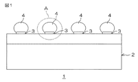
図1は、本発明の一実施形態に係る半導体装置の外観を示す側面図である。
この半導体装置1は、WL−CSP技術が適用された半導体装置であり、半導体チップ2と、半導体チップ2上に設けられた複数のポストバンプ3と、各ポストバンプ3に接合された半田ボール4とを備えている。
半導体チップ2の表層部には、SiO2からなる層間絶縁膜5が形成されている。層間絶縁膜5上には、Alからなる配線6が所定の配線パターンで形成されている。
層間絶縁膜5および配線6上には、配線6を被覆するパッシベーション膜7が形成され、パッシベーション膜7には、配線6の一部をパッシベーション膜7から露出させるための開口8が形成されている。
バリア膜9上には、Cuからなるシード膜10が形成されている。シード膜10の周縁部は、バリア膜9の周縁に対して側方に、バリア膜9の膜厚Tよりも大きいはみ出し量Dではみ出して形成されている。
ポストバンプ3は、その下面がバリア膜9に下側から支持された基端部と、当該基端部の下面と同一平面からなる下面を有し、当該下面とパッシベーション膜7との間に空間が形成されるように基端部からバリア膜9の周縁よりも側方にはみ出した周縁部とを含む。すなわち、ポストバンプ3の周縁部がバリア膜9の周縁よりも側方にはみ出していることにより、ポストバンプ3の周縁部とパッシベーション膜7との間に空間が生じている。この空間が存在することにより、ポストバンプ3の周縁部は、パッシベーション膜7との対向方向に変形可能である。よって、ポストバンプ3に応力が生じても、その応力をポストバンプ3の周縁部の変形により吸収することができる。その結果、パッシベーション膜7にクラックが生じるのを防止することができる。
また、ポストバンプ3の周縁部のはみ出し量Dは、バリア膜9の膜厚Tよりも大きい。これにより、ポストバンプ3における変形可能な周縁部の幅をバリア膜9の膜厚よりも大きく確保することができる。
まず、図3Aに示すように、CVD(Chemical Vapor Deposition:化学的気相成長)法により、層間絶縁膜5が形成される。その後、スパッタ法により、層間絶縁膜5上の全面に、Alからなる金属膜(図示せず)が形成される。そして、公知のフォトリソグラフィ技術およびエッチング技術により、層間絶縁膜5上の金属膜が選択的に除去される。これにより、層間絶縁膜5上に、所定の配線パターンを有する配線6が形成される。
たとえば、上記の実施例では、バリア膜9の材料としてTiWを用いたが、バリア膜9の材料としては、Cuの拡散に対するバリア性を有する材料であればよく、例えば、Ti(チタン)、Ta(タンタル)およびTaN(窒化タンタル)などを例示することができる。
また、配線6は、Cuを含む金属材料を用いて形成されていてもよい。Cuを含む金属材料としては、例えば、AlCu(アルミニウム/銅合金)およびCuを例示することができる。その場合、層間絶縁膜5に、その上面から掘り下がった配線溝が形成され、この配線溝に配線6が埋設されてもよい。
2 半導体チップ
3 ポストバンプ
6 配線
7 パッシベーション膜
8 開口
9 バリア膜(介在膜)
D はみ出し量
T 膜厚(介在膜の膜厚)
Claims (17)
- 半導体チップと、
前記半導体チップ上に形成された配線と、
前記配線を被覆するパッシベーション膜と、
前記パッシベーション膜を貫通して形成され、前記配線を前記パッシベーション膜から部分的に露出させるための開口と、
前記配線における前記開口に臨む部分上に形成され、その周縁部が前記パッシベーション膜における前記開口の周囲に乗り上げて形成された介在膜と、
前記介在膜上に形成されたポストバンプとを備え、
前記ポストバンプは、その下面が前記介在膜に下側から支持された基端部と、前記基端部の前記下面と同一平面からなる下面を有し、当該下面と前記パッシベーション膜との間に空間が形成されるように前記基端部から前記介在膜の周縁よりも側方にはみ出した周縁部とを含み、
前記介在膜の周縁に対する前記ポストバンプの周縁部のはみ出し量は、前記介在膜の膜厚よりも大きい、半導体装置。 - 半導体チップと、
前記半導体チップ上に形成された配線と、
前記配線を被覆するパッシベーション膜と、
前記パッシベーション膜を貫通して形成され、前記配線を前記パッシベーション膜から部分的に露出させるための開口と、
前記開口内において前記配線の表面および前記パッシベーション膜の側面を覆い、前記パッシベーション膜における前記開口の周囲を覆う介在膜と、
前記介在膜上に形成されたポストバンプとを備え、
前記ポストバンプは、その下面が前記介在膜に下側から支持された基端部と、前記基端部の前記下面と同一平面からなる下面を有し、当該下面と前記パッシベーション膜との間に空間が形成されるように前記基端部から前記介在膜の周縁よりも側方にはみ出した周縁部とを含み、
前記介在膜の周縁に対する前記ポストバンプの周縁部のはみ出し量は、前記介在膜の膜厚よりも大きい、半導体装置。 - 半導体チップと、
前記半導体チップ上に形成された配線と、
前記配線を被覆するパッシベーション膜と、
前記パッシベーション膜を貫通して形成され、前記配線を前記パッシベーション膜から部分的に露出させるための開口と、
前記配線における前記開口に臨む部分上に形成され、その周縁部が前記パッシベーション膜における前記開口の周囲に乗り上げて形成された介在膜と、
前記介在膜上に形成されたポストバンプとを備え、
前記ポストバンプは、その下面が前記介在膜に下側から支持された基端部と、前記基端部の前記下面と同一平面からなる下面を有し、当該下面と前記パッシベーション膜との間に空間が形成されるように前記基端部から前記介在膜の周縁よりも断面視で側方にはみ出した周縁部とを含み、
前記介在膜の周縁に対する前記ポストバンプの周縁部のはみ出し量は、前記介在膜の膜厚よりも大きい、半導体装置。 - 半導体チップと、
前記半導体チップ上に形成された配線と、
前記配線を被覆するパッシベーション膜と、
前記パッシベーション膜を貫通して形成され、前記配線を前記パッシベーション膜から部分的に露出させるための開口と、
前記配線における前記開口に臨む部分上に形成され、その周縁部が前記パッシベーション膜における前記開口の周囲に乗り上げて形成された介在膜と、
前記介在膜上に形成されたポストバンプと、
前記ポストバンプに接合された半田ボールとを備え、
前記ポストバンプは、その下面が前記介在膜に下側から支持された基端部と、前記基端部の前記下面と同一平面からなる下面を有し、当該下面と前記パッシベーション膜との間に空間が形成されるように前記基端部から前記介在膜の周縁よりも側方にはみ出した周縁部とを含み、
前記介在膜の周縁に対する前記ポストバンプの周縁部のはみ出し量は、前記介在膜の膜厚よりも大きい、半導体装置。 - 前記介在膜上に形成されたシード膜をさらに含み、
前記ポストバンプは、前記シード膜上に形成されている、請求項1〜4のいずれか一項に記載の半導体装置。 - 前記シード膜は、その周縁部が前記介在膜の周縁よりも側方にはみ出している、請求項5に記載の半導体装置。
- 前記介在膜の周縁に対する前記シード膜の周縁部のはみ出し量は、前記介在膜の膜厚よりも大きい、請求項6に記載の半導体装置。
- 前記ポストバンプの側面が、前記シード膜の側面と面一をなしている、請求項5〜7のいずれか一項に記載の半導体装置。
- 前記半導体チップの表層部に形成された層間絶縁膜をさらに含み、
前記配線は、前記層間絶縁膜上に形成されている、請求項1〜8のいずれか一項に記載の半導体装置。 - 前記ポストバンプがCuからなり、
前記介在膜が、TiW、Ti、TaおよびTaNからなる群から選択される1種からなるバリア膜である、請求項1〜9のいずれか一項に記載の半導体装置。 - 前記ポストバンプがAuからなり、
前記介在膜が、TiWからなるバリア膜である、請求項1〜9のいずれか一項に記載の半導体装置。 - 前記配線が、Alからなる、請求項1〜11のいずれか一項に記載の半導体装置。
- 前記配線が、Cuを含む金属材料を用いて形成されている、請求項1〜11のいずれか一項に記載の半導体装置。
- 前記配線が、AlCuからなる、請求項13に記載の半導体装置。
- 前記配線が、Cuからなる、請求項13に記載の半導体装置。
- 半導体チップ上に配線を形成する工程と、
前記配線を被覆するようにパッシベーション膜を形成する工程と、
前記パッシベーション膜を貫通することにより、前記配線を前記パッシベーション膜から部分的に露出させるための開口を形成する工程と、
前記配線における前記開口に臨む部分および前記パッシベーション膜に介在膜を形成する工程と、
前記介在膜上に、シード膜を形成する工程と、
前記シード膜上に、所定の形状の開口を有するレジスト膜を形成する工程と、
前記シード膜からのめっき成長により、前記レジスト膜の前記開口内にポストバンプを形成する工程と、
前記ポストバンプの形成後、前記レジスト膜を除去し、当該除去により露出した前記シード膜における前記ポストバンプから露出した部分を、前記シード膜をエッチング可能な液により除去する工程と、
前記シード膜の除去後、前記シード膜の下方の前記介在膜にまでエッチングが進行するように、前記介在膜をエッチング可能な液を前記介在膜に供給することにより、前記介在膜における前記シード膜から露出した部分を除去し、さらに前記介在膜における前記シード膜の周縁部と前記パッシベーション膜とに挟まれた部分を前記介在膜の膜厚よりも多く除去することによって、前記ポストバンプに、残った前記介在膜にその下面が下側から支持された基端部と、前記基端部の前記下面と同一平面からなる下面を有し、当該下面と前記パッシベーション膜との間に空間が形成されるように前記基端部から前記介在膜の周縁よりも側方にはみ出した周縁部とを形成する工程とを含む、半導体装置の製造方法。 - 前記介在膜をエッチングする工程では、前記シード膜の下方の前記介在膜にまでエッチングが進行するように、エッチング液の供給時間を設定する、請求項16に記載の半導体装置の製造方法。
Priority Applications (5)
| Application Number | Priority Date | Filing Date | Title |
|---|---|---|---|
| JP2007298361A JP5627835B2 (ja) | 2007-11-16 | 2007-11-16 | 半導体装置および半導体装置の製造方法 |
| US12/272,001 US9035455B2 (en) | 2007-11-16 | 2008-11-17 | Semiconductor device |
| US14/690,982 US9437544B2 (en) | 2007-11-16 | 2015-04-20 | Semiconductor device |
| US15/236,016 US9607957B2 (en) | 2007-11-16 | 2016-08-12 | Semiconductor device |
| US15/451,770 US9941231B2 (en) | 2007-11-16 | 2017-03-07 | Semiconductor device |
Applications Claiming Priority (1)
| Application Number | Priority Date | Filing Date | Title |
|---|---|---|---|
| JP2007298361A JP5627835B2 (ja) | 2007-11-16 | 2007-11-16 | 半導体装置および半導体装置の製造方法 |
Related Child Applications (1)
| Application Number | Title | Priority Date | Filing Date |
|---|---|---|---|
| JP2013183162A Division JP5891211B2 (ja) | 2013-09-04 | 2013-09-04 | 半導体装置 |
Publications (3)
| Publication Number | Publication Date |
|---|---|
| JP2009124042A JP2009124042A (ja) | 2009-06-04 |
| JP2009124042A5 JP2009124042A5 (ja) | 2010-12-24 |
| JP5627835B2 true JP5627835B2 (ja) | 2014-11-19 |
Family
ID=40641029
Family Applications (1)
| Application Number | Title | Priority Date | Filing Date |
|---|---|---|---|
| JP2007298361A Active JP5627835B2 (ja) | 2007-11-16 | 2007-11-16 | 半導体装置および半導体装置の製造方法 |
Country Status (2)
| Country | Link |
|---|---|
| US (4) | US9035455B2 (ja) |
| JP (1) | JP5627835B2 (ja) |
Families Citing this family (9)
| Publication number | Priority date | Publication date | Assignee | Title |
|---|---|---|---|---|
| JP5627835B2 (ja) * | 2007-11-16 | 2014-11-19 | ローム株式会社 | 半導体装置および半導体装置の製造方法 |
| US8592995B2 (en) * | 2009-07-02 | 2013-11-26 | Taiwan Semiconductor Manufacturing Company, Ltd. | Method and structure for adhesion of intermetallic compound (IMC) on Cu pillar bump |
| JP2011222738A (ja) * | 2010-04-09 | 2011-11-04 | Renesas Electronics Corp | 半導体装置の製造方法 |
| US9219044B2 (en) * | 2013-11-18 | 2015-12-22 | Applied Materials, Inc. | Patterned photoresist to attach a carrier wafer to a silicon device wafer |
| KR102410018B1 (ko) * | 2015-09-18 | 2022-06-16 | 삼성전자주식회사 | 반도체 패키지 |
| US10903151B2 (en) * | 2018-05-23 | 2021-01-26 | Advanced Semiconductor Engineering, Inc. | Semiconductor device package and method of manufacturing the same |
| US11139272B2 (en) | 2019-07-26 | 2021-10-05 | Sandisk Technologies Llc | Bonded assembly containing oxidation barriers and/or adhesion enhancers and methods of forming the same |
| US11393780B2 (en) | 2019-07-26 | 2022-07-19 | Sandisk Technologies Llc | Bonded assembly containing oxidation barriers, hybrid bonding, or air gap, and methods of forming the same |
| US11515273B2 (en) | 2019-07-26 | 2022-11-29 | Sandisk Technologies Llc | Bonded assembly containing oxidation barriers, hybrid bonding, or air gap, and methods of forming the same |
Family Cites Families (46)
| Publication number | Priority date | Publication date | Assignee | Title |
|---|---|---|---|---|
| JPS54111761A (en) * | 1978-02-22 | 1979-09-01 | Hitachi Ltd | Electrode construction of semiconductor device |
| JPH01278751A (ja) * | 1988-05-02 | 1989-11-09 | Matsushita Electron Corp | 半導体装置 |
| KR100199258B1 (ko) * | 1990-02-09 | 1999-06-15 | 가나이 쓰도무 | 반도체집적회로장치 |
| US5508561A (en) * | 1993-11-15 | 1996-04-16 | Nec Corporation | Apparatus for forming a double-bump structure used for flip-chip mounting |
| JPH09139387A (ja) | 1995-11-13 | 1997-05-27 | Denso Corp | 半導体装置の電極形成方法 |
| JP3321351B2 (ja) * | 1996-01-18 | 2002-09-03 | 東芝マイクロエレクトロニクス株式会社 | 半導体装置およびその製造方法 |
| US6111317A (en) * | 1996-01-18 | 2000-08-29 | Kabushiki Kaisha Toshiba | Flip-chip connection type semiconductor integrated circuit device |
| TW448524B (en) * | 1997-01-17 | 2001-08-01 | Seiko Epson Corp | Electronic component, semiconductor device, manufacturing method therefor, circuit board and electronic equipment |
| US6436300B2 (en) * | 1998-07-30 | 2002-08-20 | Motorola, Inc. | Method of manufacturing electronic components |
| JP2000133672A (ja) * | 1998-10-28 | 2000-05-12 | Seiko Epson Corp | 半導体装置及びその製造方法、回路基板並びに電子機器 |
| US6479900B1 (en) * | 1998-12-22 | 2002-11-12 | Sanyo Electric Co., Ltd. | Semiconductor device and method of manufacturing the same |
| JP4024958B2 (ja) * | 1999-03-15 | 2007-12-19 | 株式会社ルネサステクノロジ | 半導体装置および半導体実装構造体 |
| US6133136A (en) * | 1999-05-19 | 2000-10-17 | International Business Machines Corporation | Robust interconnect structure |
| US6362087B1 (en) * | 2000-05-05 | 2002-03-26 | Aptos Corporation | Method for fabricating a microelectronic fabrication having formed therein a redistribution structure |
| US6293457B1 (en) * | 2000-06-08 | 2001-09-25 | International Business Machines Corporation | Integrated method for etching of BLM titanium-tungsten alloys for CMOS devices with copper metallization |
| TW517334B (en) * | 2000-12-08 | 2003-01-11 | Nec Corp | Method of forming barrier layers for solder bumps |
| US6426556B1 (en) * | 2001-01-16 | 2002-07-30 | Megic Corporation | Reliable metal bumps on top of I/O pads with test probe marks |
| KR100643645B1 (ko) * | 2002-06-21 | 2006-11-10 | 후지쯔 가부시끼가이샤 | 반도체 장치 및 그 제조 방법 |
| US7547623B2 (en) * | 2002-06-25 | 2009-06-16 | Unitive International Limited | Methods of forming lead free solder bumps |
| JP2004031651A (ja) * | 2002-06-26 | 2004-01-29 | Sony Corp | 素子実装基板及びその製造方法 |
| JP2004071872A (ja) | 2002-08-07 | 2004-03-04 | Denso Corp | 電子装置 |
| TWI281718B (en) * | 2002-09-10 | 2007-05-21 | Advanced Semiconductor Eng | Bump and process thereof |
| JP2004152953A (ja) * | 2002-10-30 | 2004-05-27 | Citizen Watch Co Ltd | 半導体装置及びその製造方法 |
| JP2004281491A (ja) * | 2003-03-13 | 2004-10-07 | Toshiba Corp | 半導体装置及びその製造方法 |
| JP2005085857A (ja) * | 2003-09-05 | 2005-03-31 | Denso Corp | バンプを用いた電極構造 |
| JP2005116632A (ja) * | 2003-10-03 | 2005-04-28 | Rohm Co Ltd | 半導体装置の製造方法および半導体装置 |
| US20050092611A1 (en) * | 2003-11-03 | 2005-05-05 | Semitool, Inc. | Bath and method for high rate copper deposition |
| DE10355953B4 (de) * | 2003-11-29 | 2005-10-20 | Infineon Technologies Ag | Verfahren zum Galvanisieren und Kontaktvorsprungsanordnung |
| JP2005166959A (ja) * | 2003-12-03 | 2005-06-23 | Matsushita Electric Ind Co Ltd | 半導体装置およびその製造方法 |
| JP2005175128A (ja) * | 2003-12-10 | 2005-06-30 | Fujitsu Ltd | 半導体装置及びその製造方法 |
| JP4049127B2 (ja) | 2004-06-11 | 2008-02-20 | ヤマハ株式会社 | 半導体装置の製造方法 |
| US7830011B2 (en) * | 2004-03-15 | 2010-11-09 | Yamaha Corporation | Semiconductor element and wafer level chip size package therefor |
| JP2006100552A (ja) * | 2004-09-29 | 2006-04-13 | Rohm Co Ltd | 配線基板および半導体装置 |
| JP2006278551A (ja) | 2005-03-28 | 2006-10-12 | Fujitsu Ltd | 半導体装置及びその製造方法 |
| TWI288447B (en) * | 2005-04-12 | 2007-10-11 | Siliconware Precision Industries Co Ltd | Conductive bump structure for semiconductor device and fabrication method thereof |
| JP2007019473A (ja) * | 2005-06-10 | 2007-01-25 | Nec Electronics Corp | 半導体装置 |
| US7622309B2 (en) * | 2005-06-28 | 2009-11-24 | Freescale Semiconductor, Inc. | Mechanical integrity evaluation of low-k devices with bump shear |
| TWI339419B (en) * | 2005-12-05 | 2011-03-21 | Megica Corp | Semiconductor chip |
| JP4247690B2 (ja) * | 2006-06-15 | 2009-04-02 | ソニー株式会社 | 電子部品及その製造方法 |
| JP4354469B2 (ja) * | 2006-08-11 | 2009-10-28 | シャープ株式会社 | 半導体装置および半導体装置の製造方法 |
| JP5627835B2 (ja) * | 2007-11-16 | 2014-11-19 | ローム株式会社 | 半導体装置および半導体装置の製造方法 |
| US7985671B2 (en) * | 2008-12-29 | 2011-07-26 | International Business Machines Corporation | Structures and methods for improving solder bump connections in semiconductor devices |
| US7989356B2 (en) * | 2009-03-24 | 2011-08-02 | Stats Chippac, Ltd. | Semiconductor device and method of forming enhanced UBM structure for improving solder joint reliability |
| US8669137B2 (en) * | 2011-04-01 | 2014-03-11 | International Business Machines Corporation | Copper post solder bumps on substrate |
| US9087701B2 (en) * | 2011-04-30 | 2015-07-21 | Stats Chippac, Ltd. | Semiconductor device and method of embedding TSV semiconductor die within substrate for vertical interconnect in POP |
| US8643150B1 (en) * | 2012-02-15 | 2014-02-04 | Maxim Integrated Products, Inc. | Wafer-level package device having solder bump assemblies that include an inner pillar structure |
-
2007
- 2007-11-16 JP JP2007298361A patent/JP5627835B2/ja active Active
-
2008
- 2008-11-17 US US12/272,001 patent/US9035455B2/en active Active
-
2015
- 2015-04-20 US US14/690,982 patent/US9437544B2/en active Active
-
2016
- 2016-08-12 US US15/236,016 patent/US9607957B2/en active Active
-
2017
- 2017-03-07 US US15/451,770 patent/US9941231B2/en active Active
Also Published As
| Publication number | Publication date |
|---|---|
| US20090127709A1 (en) | 2009-05-21 |
| US20160351519A1 (en) | 2016-12-01 |
| US9035455B2 (en) | 2015-05-19 |
| US9437544B2 (en) | 2016-09-06 |
| US9941231B2 (en) | 2018-04-10 |
| US20170179060A1 (en) | 2017-06-22 |
| US9607957B2 (en) | 2017-03-28 |
| US20150228575A1 (en) | 2015-08-13 |
| JP2009124042A (ja) | 2009-06-04 |
Similar Documents
| Publication | Publication Date | Title |
|---|---|---|
| JP5627835B2 (ja) | 半導体装置および半導体装置の製造方法 | |
| US7582971B2 (en) | Semiconductor device and manufacturing method of the same | |
| US10074584B2 (en) | Method of forming a semiconductor component comprising a second passivation layer having a first opening exposing a bond pad and a plurality of second openings exposing a top surface of an underlying first passivation layer | |
| US7485967B2 (en) | Semiconductor device with via hole for electric connection | |
| KR100647760B1 (ko) | 반도체 장치 및 그 제조 방법 | |
| JP4373866B2 (ja) | 半導体装置の製造方法 | |
| KR100881199B1 (ko) | 관통전극을 구비하는 반도체 장치 및 이를 제조하는 방법 | |
| US8587119B2 (en) | Conductive feature for semiconductor substrate and method of manufacture | |
| KR101855570B1 (ko) | 반도체 디바이스 구조물 및 그것의 형성 방법 | |
| JP2006516824A (ja) | ウエハ・スクライブ領域の金属低減 | |
| JP2012147006A (ja) | 能動領域ボンディングの両立性のある高電流構造体 | |
| US20150287685A1 (en) | Solder Pad for Semiconductor Device Package | |
| JP2007221080A (ja) | 半導体装置およびその製造方法 | |
| JP2010251791A (ja) | 半導体装置及びその製造方法 | |
| JP2010016224A (ja) | 半導体装置および半導体装置の製造方法 | |
| JP5036127B2 (ja) | 半導体装置の製造方法 | |
| JP5891211B2 (ja) | 半導体装置 | |
| KR100896841B1 (ko) | 반도체 소자 제조시 본드 패드 형성방법 | |
| JP2004281982A (ja) | 半導体装置及びその製造方法 | |
| JP2005129862A (ja) | 半導体パッケージの製造方法、半導体パッケージ | |
| JP2008028109A (ja) | 半導体装置及び半導体装置の製造方法 | |
| JP5258735B2 (ja) | 半導体装置 | |
| JP2006179661A (ja) | 半導体装置、半導体装置の製造方法、及び半導体パッケージ |
Legal Events
| Date | Code | Title | Description |
|---|---|---|---|
| A521 | Request for written amendment filed |
Free format text: JAPANESE INTERMEDIATE CODE: A523 Effective date: 20101110 |
|
| A621 | Written request for application examination |
Free format text: JAPANESE INTERMEDIATE CODE: A621 Effective date: 20101112 |
|
| A977 | Report on retrieval |
Free format text: JAPANESE INTERMEDIATE CODE: A971007 Effective date: 20120306 |
|
| A131 | Notification of reasons for refusal |
Free format text: JAPANESE INTERMEDIATE CODE: A131 Effective date: 20120315 |
|
| A521 | Request for written amendment filed |
Free format text: JAPANESE INTERMEDIATE CODE: A523 Effective date: 20120507 |
|
| A131 | Notification of reasons for refusal |
Free format text: JAPANESE INTERMEDIATE CODE: A131 Effective date: 20120802 |
|
| A521 | Request for written amendment filed |
Free format text: JAPANESE INTERMEDIATE CODE: A523 Effective date: 20120910 |
|
| A02 | Decision of refusal |
Free format text: JAPANESE INTERMEDIATE CODE: A02 Effective date: 20130606 |
|
| A521 | Request for written amendment filed |
Free format text: JAPANESE INTERMEDIATE CODE: A523 Effective date: 20130904 |
|
| A911 | Transfer to examiner for re-examination before appeal (zenchi) |
Free format text: JAPANESE INTERMEDIATE CODE: A911 Effective date: 20130911 |
|
| A912 | Re-examination (zenchi) completed and case transferred to appeal board |
Free format text: JAPANESE INTERMEDIATE CODE: A912 Effective date: 20131129 |
|
| A61 | First payment of annual fees (during grant procedure) |
Free format text: JAPANESE INTERMEDIATE CODE: A61 Effective date: 20141001 |
|
| R150 | Certificate of patent or registration of utility model |
Ref document number: 5627835 Country of ref document: JP Free format text: JAPANESE INTERMEDIATE CODE: R150 |
|
| R250 | Receipt of annual fees |
Free format text: JAPANESE INTERMEDIATE CODE: R250 |
|
| R250 | Receipt of annual fees |
Free format text: JAPANESE INTERMEDIATE CODE: R250 |
|
| R250 | Receipt of annual fees |
Free format text: JAPANESE INTERMEDIATE CODE: R250 |
|
| R250 | Receipt of annual fees |
Free format text: JAPANESE INTERMEDIATE CODE: R250 |
|
| R250 | Receipt of annual fees |
Free format text: JAPANESE INTERMEDIATE CODE: R250 |