JP2010010700A - 半導体装置の製造方法及び半導体装置 - Google Patents
半導体装置の製造方法及び半導体装置 Download PDFInfo
- Publication number
- JP2010010700A JP2010010700A JP2009212140A JP2009212140A JP2010010700A JP 2010010700 A JP2010010700 A JP 2010010700A JP 2009212140 A JP2009212140 A JP 2009212140A JP 2009212140 A JP2009212140 A JP 2009212140A JP 2010010700 A JP2010010700 A JP 2010010700A
- Authority
- JP
- Japan
- Prior art keywords
- film
- metal film
- insulating film
- barrier metal
- semiconductor device
- Prior art date
- Legal status (The legal status is an assumption and is not a legal conclusion. Google has not performed a legal analysis and makes no representation as to the accuracy of the status listed.)
- Granted
Links
Images


Classifications
-
- H—ELECTRICITY
- H01—ELECTRIC ELEMENTS
- H01L—SEMICONDUCTOR DEVICES NOT COVERED BY CLASS H10
- H01L21/00—Processes or apparatus adapted for the manufacture or treatment of semiconductor or solid state devices or of parts thereof
- H01L21/02—Manufacture or treatment of semiconductor devices or of parts thereof
- H01L21/04—Manufacture or treatment of semiconductor devices or of parts thereof the devices having at least one potential-jump barrier or surface barrier, e.g. PN junction, depletion layer or carrier concentration layer
- H01L21/18—Manufacture or treatment of semiconductor devices or of parts thereof the devices having at least one potential-jump barrier or surface barrier, e.g. PN junction, depletion layer or carrier concentration layer the devices having semiconductor bodies comprising elements of Group IV of the Periodic System or AIIIBV compounds with or without impurities, e.g. doping materials
- H01L21/30—Treatment of semiconductor bodies using processes or apparatus not provided for in groups H01L21/20 - H01L21/26
- H01L21/31—Treatment of semiconductor bodies using processes or apparatus not provided for in groups H01L21/20 - H01L21/26 to form insulating layers thereon, e.g. for masking or by using photolithographic techniques; After treatment of these layers; Selection of materials for these layers
- H01L21/314—Inorganic layers
- H01L21/316—Inorganic layers composed of oxides or glassy oxides or oxide based glass
- H01L21/31604—Deposition from a gas or vapour
- H01L21/31616—Deposition of Al2O3
-
- C—CHEMISTRY; METALLURGY
- C23—COATING METALLIC MATERIAL; COATING MATERIAL WITH METALLIC MATERIAL; CHEMICAL SURFACE TREATMENT; DIFFUSION TREATMENT OF METALLIC MATERIAL; COATING BY VACUUM EVAPORATION, BY SPUTTERING, BY ION IMPLANTATION OR BY CHEMICAL VAPOUR DEPOSITION, IN GENERAL; INHIBITING CORROSION OF METALLIC MATERIAL OR INCRUSTATION IN GENERAL
- C23C—COATING METALLIC MATERIAL; COATING MATERIAL WITH METALLIC MATERIAL; SURFACE TREATMENT OF METALLIC MATERIAL BY DIFFUSION INTO THE SURFACE, BY CHEMICAL CONVERSION OR SUBSTITUTION; COATING BY VACUUM EVAPORATION, BY SPUTTERING, BY ION IMPLANTATION OR BY CHEMICAL VAPOUR DEPOSITION, IN GENERAL
- C23C16/00—Chemical coating by decomposition of gaseous compounds, without leaving reaction products of surface material in the coating, i.e. chemical vapour deposition [CVD] processes
- C23C16/04—Coating on selected surface areas, e.g. using masks
- C23C16/045—Coating cavities or hollow spaces, e.g. interior of tubes; Infiltration of porous substrates
-
- C—CHEMISTRY; METALLURGY
- C23—COATING METALLIC MATERIAL; COATING MATERIAL WITH METALLIC MATERIAL; CHEMICAL SURFACE TREATMENT; DIFFUSION TREATMENT OF METALLIC MATERIAL; COATING BY VACUUM EVAPORATION, BY SPUTTERING, BY ION IMPLANTATION OR BY CHEMICAL VAPOUR DEPOSITION, IN GENERAL; INHIBITING CORROSION OF METALLIC MATERIAL OR INCRUSTATION IN GENERAL
- C23C—COATING METALLIC MATERIAL; COATING MATERIAL WITH METALLIC MATERIAL; SURFACE TREATMENT OF METALLIC MATERIAL BY DIFFUSION INTO THE SURFACE, BY CHEMICAL CONVERSION OR SUBSTITUTION; COATING BY VACUUM EVAPORATION, BY SPUTTERING, BY ION IMPLANTATION OR BY CHEMICAL VAPOUR DEPOSITION, IN GENERAL
- C23C16/00—Chemical coating by decomposition of gaseous compounds, without leaving reaction products of surface material in the coating, i.e. chemical vapour deposition [CVD] processes
- C23C16/44—Chemical coating by decomposition of gaseous compounds, without leaving reaction products of surface material in the coating, i.e. chemical vapour deposition [CVD] processes characterised by the method of coating
- C23C16/455—Chemical coating by decomposition of gaseous compounds, without leaving reaction products of surface material in the coating, i.e. chemical vapour deposition [CVD] processes characterised by the method of coating characterised by the method used for introducing gases into reaction chamber or for modifying gas flows in reaction chamber
- C23C16/45523—Pulsed gas flow or change of composition over time
- C23C16/45525—Atomic layer deposition [ALD]
- C23C16/45527—Atomic layer deposition [ALD] characterized by the ALD cycle, e.g. different flows or temperatures during half-reactions, unusual pulsing sequence, use of precursor mixtures or auxiliary reactants or activations
- C23C16/45536—Use of plasma, radiation or electromagnetic fields
-
- C—CHEMISTRY; METALLURGY
- C23—COATING METALLIC MATERIAL; COATING MATERIAL WITH METALLIC MATERIAL; CHEMICAL SURFACE TREATMENT; DIFFUSION TREATMENT OF METALLIC MATERIAL; COATING BY VACUUM EVAPORATION, BY SPUTTERING, BY ION IMPLANTATION OR BY CHEMICAL VAPOUR DEPOSITION, IN GENERAL; INHIBITING CORROSION OF METALLIC MATERIAL OR INCRUSTATION IN GENERAL
- C23C—COATING METALLIC MATERIAL; COATING MATERIAL WITH METALLIC MATERIAL; SURFACE TREATMENT OF METALLIC MATERIAL BY DIFFUSION INTO THE SURFACE, BY CHEMICAL CONVERSION OR SUBSTITUTION; COATING BY VACUUM EVAPORATION, BY SPUTTERING, BY ION IMPLANTATION OR BY CHEMICAL VAPOUR DEPOSITION, IN GENERAL
- C23C16/00—Chemical coating by decomposition of gaseous compounds, without leaving reaction products of surface material in the coating, i.e. chemical vapour deposition [CVD] processes
- C23C16/44—Chemical coating by decomposition of gaseous compounds, without leaving reaction products of surface material in the coating, i.e. chemical vapour deposition [CVD] processes characterised by the method of coating
- C23C16/48—Chemical coating by decomposition of gaseous compounds, without leaving reaction products of surface material in the coating, i.e. chemical vapour deposition [CVD] processes characterised by the method of coating by irradiation, e.g. photolysis, radiolysis, particle radiation
- C23C16/482—Chemical coating by decomposition of gaseous compounds, without leaving reaction products of surface material in the coating, i.e. chemical vapour deposition [CVD] processes characterised by the method of coating by irradiation, e.g. photolysis, radiolysis, particle radiation using incoherent light, UV to IR, e.g. lamps
-
- H—ELECTRICITY
- H01—ELECTRIC ELEMENTS
- H01L—SEMICONDUCTOR DEVICES NOT COVERED BY CLASS H10
- H01L21/00—Processes or apparatus adapted for the manufacture or treatment of semiconductor or solid state devices or of parts thereof
- H01L21/02—Manufacture or treatment of semiconductor devices or of parts thereof
- H01L21/02104—Forming layers
- H01L21/02107—Forming insulating materials on a substrate
- H01L21/02109—Forming insulating materials on a substrate characterised by the type of layer, e.g. type of material, porous/non-porous, pre-cursors, mixtures or laminates
- H01L21/02112—Forming insulating materials on a substrate characterised by the type of layer, e.g. type of material, porous/non-porous, pre-cursors, mixtures or laminates characterised by the material of the layer
- H01L21/02172—Forming insulating materials on a substrate characterised by the type of layer, e.g. type of material, porous/non-porous, pre-cursors, mixtures or laminates characterised by the material of the layer the material containing at least one metal element, e.g. metal oxides, metal nitrides, metal oxynitrides or metal carbides
- H01L21/02175—Forming insulating materials on a substrate characterised by the type of layer, e.g. type of material, porous/non-porous, pre-cursors, mixtures or laminates characterised by the material of the layer the material containing at least one metal element, e.g. metal oxides, metal nitrides, metal oxynitrides or metal carbides characterised by the metal
- H01L21/02178—Forming insulating materials on a substrate characterised by the type of layer, e.g. type of material, porous/non-porous, pre-cursors, mixtures or laminates characterised by the material of the layer the material containing at least one metal element, e.g. metal oxides, metal nitrides, metal oxynitrides or metal carbides characterised by the metal the material containing aluminium, e.g. Al2O3
-
- H—ELECTRICITY
- H01—ELECTRIC ELEMENTS
- H01L—SEMICONDUCTOR DEVICES NOT COVERED BY CLASS H10
- H01L21/00—Processes or apparatus adapted for the manufacture or treatment of semiconductor or solid state devices or of parts thereof
- H01L21/02—Manufacture or treatment of semiconductor devices or of parts thereof
- H01L21/02104—Forming layers
- H01L21/02107—Forming insulating materials on a substrate
- H01L21/02109—Forming insulating materials on a substrate characterised by the type of layer, e.g. type of material, porous/non-porous, pre-cursors, mixtures or laminates
- H01L21/02112—Forming insulating materials on a substrate characterised by the type of layer, e.g. type of material, porous/non-porous, pre-cursors, mixtures or laminates characterised by the material of the layer
- H01L21/02172—Forming insulating materials on a substrate characterised by the type of layer, e.g. type of material, porous/non-porous, pre-cursors, mixtures or laminates characterised by the material of the layer the material containing at least one metal element, e.g. metal oxides, metal nitrides, metal oxynitrides or metal carbides
- H01L21/02175—Forming insulating materials on a substrate characterised by the type of layer, e.g. type of material, porous/non-porous, pre-cursors, mixtures or laminates characterised by the material of the layer the material containing at least one metal element, e.g. metal oxides, metal nitrides, metal oxynitrides or metal carbides characterised by the metal
- H01L21/02186—Forming insulating materials on a substrate characterised by the type of layer, e.g. type of material, porous/non-porous, pre-cursors, mixtures or laminates characterised by the material of the layer the material containing at least one metal element, e.g. metal oxides, metal nitrides, metal oxynitrides or metal carbides characterised by the metal the material containing titanium, e.g. TiO2
-
- H—ELECTRICITY
- H01—ELECTRIC ELEMENTS
- H01L—SEMICONDUCTOR DEVICES NOT COVERED BY CLASS H10
- H01L21/00—Processes or apparatus adapted for the manufacture or treatment of semiconductor or solid state devices or of parts thereof
- H01L21/02—Manufacture or treatment of semiconductor devices or of parts thereof
- H01L21/02104—Forming layers
- H01L21/02107—Forming insulating materials on a substrate
- H01L21/02225—Forming insulating materials on a substrate characterised by the process for the formation of the insulating layer
- H01L21/02227—Forming insulating materials on a substrate characterised by the process for the formation of the insulating layer formation by a process other than a deposition process
- H01L21/0223—Forming insulating materials on a substrate characterised by the process for the formation of the insulating layer formation by a process other than a deposition process formation by oxidation, e.g. oxidation of the substrate
- H01L21/02244—Forming insulating materials on a substrate characterised by the process for the formation of the insulating layer formation by a process other than a deposition process formation by oxidation, e.g. oxidation of the substrate of a metallic layer
-
- H—ELECTRICITY
- H01—ELECTRIC ELEMENTS
- H01L—SEMICONDUCTOR DEVICES NOT COVERED BY CLASS H10
- H01L21/00—Processes or apparatus adapted for the manufacture or treatment of semiconductor or solid state devices or of parts thereof
- H01L21/02—Manufacture or treatment of semiconductor devices or of parts thereof
- H01L21/02104—Forming layers
- H01L21/02107—Forming insulating materials on a substrate
- H01L21/02225—Forming insulating materials on a substrate characterised by the process for the formation of the insulating layer
- H01L21/02227—Forming insulating materials on a substrate characterised by the process for the formation of the insulating layer formation by a process other than a deposition process
- H01L21/02255—Forming insulating materials on a substrate characterised by the process for the formation of the insulating layer formation by a process other than a deposition process formation by thermal treatment
-
- H—ELECTRICITY
- H01—ELECTRIC ELEMENTS
- H01L—SEMICONDUCTOR DEVICES NOT COVERED BY CLASS H10
- H01L21/00—Processes or apparatus adapted for the manufacture or treatment of semiconductor or solid state devices or of parts thereof
- H01L21/02—Manufacture or treatment of semiconductor devices or of parts thereof
- H01L21/04—Manufacture or treatment of semiconductor devices or of parts thereof the devices having at least one potential-jump barrier or surface barrier, e.g. PN junction, depletion layer or carrier concentration layer
- H01L21/18—Manufacture or treatment of semiconductor devices or of parts thereof the devices having at least one potential-jump barrier or surface barrier, e.g. PN junction, depletion layer or carrier concentration layer the devices having semiconductor bodies comprising elements of Group IV of the Periodic System or AIIIBV compounds with or without impurities, e.g. doping materials
- H01L21/28—Manufacture of electrodes on semiconductor bodies using processes or apparatus not provided for in groups H01L21/20 - H01L21/268
- H01L21/283—Deposition of conductive or insulating materials for electrodes conducting electric current
- H01L21/285—Deposition of conductive or insulating materials for electrodes conducting electric current from a gas or vapour, e.g. condensation
- H01L21/28506—Deposition of conductive or insulating materials for electrodes conducting electric current from a gas or vapour, e.g. condensation of conductive layers
- H01L21/28512—Deposition of conductive or insulating materials for electrodes conducting electric current from a gas or vapour, e.g. condensation of conductive layers on semiconductor bodies comprising elements of Group IV of the Periodic System
- H01L21/28556—Deposition of conductive or insulating materials for electrodes conducting electric current from a gas or vapour, e.g. condensation of conductive layers on semiconductor bodies comprising elements of Group IV of the Periodic System by chemical means, e.g. CVD, LPCVD, PECVD, laser CVD
- H01L21/28562—Selective deposition
-
- H—ELECTRICITY
- H01—ELECTRIC ELEMENTS
- H01L—SEMICONDUCTOR DEVICES NOT COVERED BY CLASS H10
- H01L21/00—Processes or apparatus adapted for the manufacture or treatment of semiconductor or solid state devices or of parts thereof
- H01L21/67—Apparatus specially adapted for handling semiconductor or electric solid state devices during manufacture or treatment thereof; Apparatus specially adapted for handling wafers during manufacture or treatment of semiconductor or electric solid state devices or components ; Apparatus not specifically provided for elsewhere
- H01L21/677—Apparatus specially adapted for handling semiconductor or electric solid state devices during manufacture or treatment thereof; Apparatus specially adapted for handling wafers during manufacture or treatment of semiconductor or electric solid state devices or components ; Apparatus not specifically provided for elsewhere for conveying, e.g. between different workstations
- H01L21/67739—Apparatus specially adapted for handling semiconductor or electric solid state devices during manufacture or treatment thereof; Apparatus specially adapted for handling wafers during manufacture or treatment of semiconductor or electric solid state devices or components ; Apparatus not specifically provided for elsewhere for conveying, e.g. between different workstations into and out of processing chamber
- H01L21/67748—Apparatus specially adapted for handling semiconductor or electric solid state devices during manufacture or treatment thereof; Apparatus specially adapted for handling wafers during manufacture or treatment of semiconductor or electric solid state devices or components ; Apparatus not specifically provided for elsewhere for conveying, e.g. between different workstations into and out of processing chamber horizontal transfer of a single workpiece
-
- H—ELECTRICITY
- H01—ELECTRIC ELEMENTS
- H01L—SEMICONDUCTOR DEVICES NOT COVERED BY CLASS H10
- H01L21/00—Processes or apparatus adapted for the manufacture or treatment of semiconductor or solid state devices or of parts thereof
- H01L21/67—Apparatus specially adapted for handling semiconductor or electric solid state devices during manufacture or treatment thereof; Apparatus specially adapted for handling wafers during manufacture or treatment of semiconductor or electric solid state devices or components ; Apparatus not specifically provided for elsewhere
- H01L21/683—Apparatus specially adapted for handling semiconductor or electric solid state devices during manufacture or treatment thereof; Apparatus specially adapted for handling wafers during manufacture or treatment of semiconductor or electric solid state devices or components ; Apparatus not specifically provided for elsewhere for supporting or gripping
- H01L21/687—Apparatus specially adapted for handling semiconductor or electric solid state devices during manufacture or treatment thereof; Apparatus specially adapted for handling wafers during manufacture or treatment of semiconductor or electric solid state devices or components ; Apparatus not specifically provided for elsewhere for supporting or gripping using mechanical means, e.g. chucks, clamps or pinches
- H01L21/68714—Apparatus specially adapted for handling semiconductor or electric solid state devices during manufacture or treatment thereof; Apparatus specially adapted for handling wafers during manufacture or treatment of semiconductor or electric solid state devices or components ; Apparatus not specifically provided for elsewhere for supporting or gripping using mechanical means, e.g. chucks, clamps or pinches the wafers being placed on a susceptor, stage or support
- H01L21/68742—Apparatus specially adapted for handling semiconductor or electric solid state devices during manufacture or treatment thereof; Apparatus specially adapted for handling wafers during manufacture or treatment of semiconductor or electric solid state devices or components ; Apparatus not specifically provided for elsewhere for supporting or gripping using mechanical means, e.g. chucks, clamps or pinches the wafers being placed on a susceptor, stage or support characterised by a lifting arrangement, e.g. lift pins
-
- H—ELECTRICITY
- H01—ELECTRIC ELEMENTS
- H01L—SEMICONDUCTOR DEVICES NOT COVERED BY CLASS H10
- H01L21/00—Processes or apparatus adapted for the manufacture or treatment of semiconductor or solid state devices or of parts thereof
- H01L21/67—Apparatus specially adapted for handling semiconductor or electric solid state devices during manufacture or treatment thereof; Apparatus specially adapted for handling wafers during manufacture or treatment of semiconductor or electric solid state devices or components ; Apparatus not specifically provided for elsewhere
- H01L21/683—Apparatus specially adapted for handling semiconductor or electric solid state devices during manufacture or treatment thereof; Apparatus specially adapted for handling wafers during manufacture or treatment of semiconductor or electric solid state devices or components ; Apparatus not specifically provided for elsewhere for supporting or gripping
- H01L21/687—Apparatus specially adapted for handling semiconductor or electric solid state devices during manufacture or treatment thereof; Apparatus specially adapted for handling wafers during manufacture or treatment of semiconductor or electric solid state devices or components ; Apparatus not specifically provided for elsewhere for supporting or gripping using mechanical means, e.g. chucks, clamps or pinches
- H01L21/68714—Apparatus specially adapted for handling semiconductor or electric solid state devices during manufacture or treatment thereof; Apparatus specially adapted for handling wafers during manufacture or treatment of semiconductor or electric solid state devices or components ; Apparatus not specifically provided for elsewhere for supporting or gripping using mechanical means, e.g. chucks, clamps or pinches the wafers being placed on a susceptor, stage or support
- H01L21/68764—Apparatus specially adapted for handling semiconductor or electric solid state devices during manufacture or treatment thereof; Apparatus specially adapted for handling wafers during manufacture or treatment of semiconductor or electric solid state devices or components ; Apparatus not specifically provided for elsewhere for supporting or gripping using mechanical means, e.g. chucks, clamps or pinches the wafers being placed on a susceptor, stage or support characterised by a movable susceptor, stage or support, others than those only rotating on their own vertical axis, e.g. susceptors on a rotating caroussel
-
- H—ELECTRICITY
- H01—ELECTRIC ELEMENTS
- H01L—SEMICONDUCTOR DEVICES NOT COVERED BY CLASS H10
- H01L21/00—Processes or apparatus adapted for the manufacture or treatment of semiconductor or solid state devices or of parts thereof
- H01L21/67—Apparatus specially adapted for handling semiconductor or electric solid state devices during manufacture or treatment thereof; Apparatus specially adapted for handling wafers during manufacture or treatment of semiconductor or electric solid state devices or components ; Apparatus not specifically provided for elsewhere
- H01L21/683—Apparatus specially adapted for handling semiconductor or electric solid state devices during manufacture or treatment thereof; Apparatus specially adapted for handling wafers during manufacture or treatment of semiconductor or electric solid state devices or components ; Apparatus not specifically provided for elsewhere for supporting or gripping
- H01L21/687—Apparatus specially adapted for handling semiconductor or electric solid state devices during manufacture or treatment thereof; Apparatus specially adapted for handling wafers during manufacture or treatment of semiconductor or electric solid state devices or components ; Apparatus not specifically provided for elsewhere for supporting or gripping using mechanical means, e.g. chucks, clamps or pinches
- H01L21/68714—Apparatus specially adapted for handling semiconductor or electric solid state devices during manufacture or treatment thereof; Apparatus specially adapted for handling wafers during manufacture or treatment of semiconductor or electric solid state devices or components ; Apparatus not specifically provided for elsewhere for supporting or gripping using mechanical means, e.g. chucks, clamps or pinches the wafers being placed on a susceptor, stage or support
- H01L21/68771—Apparatus specially adapted for handling semiconductor or electric solid state devices during manufacture or treatment thereof; Apparatus specially adapted for handling wafers during manufacture or treatment of semiconductor or electric solid state devices or components ; Apparatus not specifically provided for elsewhere for supporting or gripping using mechanical means, e.g. chucks, clamps or pinches the wafers being placed on a susceptor, stage or support characterised by supporting more than one semiconductor substrate
-
- H—ELECTRICITY
- H01—ELECTRIC ELEMENTS
- H01L—SEMICONDUCTOR DEVICES NOT COVERED BY CLASS H10
- H01L21/00—Processes or apparatus adapted for the manufacture or treatment of semiconductor or solid state devices or of parts thereof
- H01L21/70—Manufacture or treatment of devices consisting of a plurality of solid state components formed in or on a common substrate or of parts thereof; Manufacture of integrated circuit devices or of parts thereof
- H01L21/71—Manufacture of specific parts of devices defined in group H01L21/70
- H01L21/768—Applying interconnections to be used for carrying current between separate components within a device comprising conductors and dielectrics
- H01L21/76801—Applying interconnections to be used for carrying current between separate components within a device comprising conductors and dielectrics characterised by the formation and the after-treatment of the dielectrics, e.g. smoothing
- H01L21/76802—Applying interconnections to be used for carrying current between separate components within a device comprising conductors and dielectrics characterised by the formation and the after-treatment of the dielectrics, e.g. smoothing by forming openings in dielectrics
- H01L21/76814—Applying interconnections to be used for carrying current between separate components within a device comprising conductors and dielectrics characterised by the formation and the after-treatment of the dielectrics, e.g. smoothing by forming openings in dielectrics post-treatment or after-treatment, e.g. cleaning or removal of oxides on underlying conductors
-
- H—ELECTRICITY
- H01—ELECTRIC ELEMENTS
- H01L—SEMICONDUCTOR DEVICES NOT COVERED BY CLASS H10
- H01L21/00—Processes or apparatus adapted for the manufacture or treatment of semiconductor or solid state devices or of parts thereof
- H01L21/70—Manufacture or treatment of devices consisting of a plurality of solid state components formed in or on a common substrate or of parts thereof; Manufacture of integrated circuit devices or of parts thereof
- H01L21/71—Manufacture of specific parts of devices defined in group H01L21/70
- H01L21/768—Applying interconnections to be used for carrying current between separate components within a device comprising conductors and dielectrics
- H01L21/76801—Applying interconnections to be used for carrying current between separate components within a device comprising conductors and dielectrics characterised by the formation and the after-treatment of the dielectrics, e.g. smoothing
- H01L21/76822—Modification of the material of dielectric layers, e.g. grading, after-treatment to improve the stability of the layers, to increase their density etc.
- H01L21/76828—Modification of the material of dielectric layers, e.g. grading, after-treatment to improve the stability of the layers, to increase their density etc. thermal treatment
-
- H—ELECTRICITY
- H01—ELECTRIC ELEMENTS
- H01L—SEMICONDUCTOR DEVICES NOT COVERED BY CLASS H10
- H01L21/00—Processes or apparatus adapted for the manufacture or treatment of semiconductor or solid state devices or of parts thereof
- H01L21/70—Manufacture or treatment of devices consisting of a plurality of solid state components formed in or on a common substrate or of parts thereof; Manufacture of integrated circuit devices or of parts thereof
- H01L21/71—Manufacture of specific parts of devices defined in group H01L21/70
- H01L21/768—Applying interconnections to be used for carrying current between separate components within a device comprising conductors and dielectrics
- H01L21/76801—Applying interconnections to be used for carrying current between separate components within a device comprising conductors and dielectrics characterised by the formation and the after-treatment of the dielectrics, e.g. smoothing
- H01L21/76829—Applying interconnections to be used for carrying current between separate components within a device comprising conductors and dielectrics characterised by the formation and the after-treatment of the dielectrics, e.g. smoothing characterised by the formation of thin functional dielectric layers, e.g. dielectric etch-stop, barrier, capping or liner layers
- H01L21/76831—Applying interconnections to be used for carrying current between separate components within a device comprising conductors and dielectrics characterised by the formation and the after-treatment of the dielectrics, e.g. smoothing characterised by the formation of thin functional dielectric layers, e.g. dielectric etch-stop, barrier, capping or liner layers in via holes or trenches, e.g. non-conductive sidewall liners
-
- H—ELECTRICITY
- H01—ELECTRIC ELEMENTS
- H01L—SEMICONDUCTOR DEVICES NOT COVERED BY CLASS H10
- H01L21/00—Processes or apparatus adapted for the manufacture or treatment of semiconductor or solid state devices or of parts thereof
- H01L21/70—Manufacture or treatment of devices consisting of a plurality of solid state components formed in or on a common substrate or of parts thereof; Manufacture of integrated circuit devices or of parts thereof
- H01L21/71—Manufacture of specific parts of devices defined in group H01L21/70
- H01L21/768—Applying interconnections to be used for carrying current between separate components within a device comprising conductors and dielectrics
- H01L21/76801—Applying interconnections to be used for carrying current between separate components within a device comprising conductors and dielectrics characterised by the formation and the after-treatment of the dielectrics, e.g. smoothing
- H01L21/76835—Combinations of two or more different dielectric layers having a low dielectric constant
-
- H—ELECTRICITY
- H01—ELECTRIC ELEMENTS
- H01L—SEMICONDUCTOR DEVICES NOT COVERED BY CLASS H10
- H01L21/00—Processes or apparatus adapted for the manufacture or treatment of semiconductor or solid state devices or of parts thereof
- H01L21/70—Manufacture or treatment of devices consisting of a plurality of solid state components formed in or on a common substrate or of parts thereof; Manufacture of integrated circuit devices or of parts thereof
- H01L21/71—Manufacture of specific parts of devices defined in group H01L21/70
- H01L21/768—Applying interconnections to be used for carrying current between separate components within a device comprising conductors and dielectrics
- H01L21/76838—Applying interconnections to be used for carrying current between separate components within a device comprising conductors and dielectrics characterised by the formation and the after-treatment of the conductors
- H01L21/76841—Barrier, adhesion or liner layers
- H01L21/76843—Barrier, adhesion or liner layers formed in openings in a dielectric
- H01L21/76846—Layer combinations
-
- H—ELECTRICITY
- H01—ELECTRIC ELEMENTS
- H01L—SEMICONDUCTOR DEVICES NOT COVERED BY CLASS H10
- H01L21/00—Processes or apparatus adapted for the manufacture or treatment of semiconductor or solid state devices or of parts thereof
- H01L21/70—Manufacture or treatment of devices consisting of a plurality of solid state components formed in or on a common substrate or of parts thereof; Manufacture of integrated circuit devices or of parts thereof
- H01L21/71—Manufacture of specific parts of devices defined in group H01L21/70
- H01L21/768—Applying interconnections to be used for carrying current between separate components within a device comprising conductors and dielectrics
- H01L21/76838—Applying interconnections to be used for carrying current between separate components within a device comprising conductors and dielectrics characterised by the formation and the after-treatment of the conductors
- H01L21/76841—Barrier, adhesion or liner layers
- H01L21/76853—Barrier, adhesion or liner layers characterized by particular after-treatment steps
- H01L21/76855—After-treatment introducing at least one additional element into the layer
- H01L21/76858—After-treatment introducing at least one additional element into the layer by diffusing alloying elements
-
- H—ELECTRICITY
- H01—ELECTRIC ELEMENTS
- H01L—SEMICONDUCTOR DEVICES NOT COVERED BY CLASS H10
- H01L21/00—Processes or apparatus adapted for the manufacture or treatment of semiconductor or solid state devices or of parts thereof
- H01L21/70—Manufacture or treatment of devices consisting of a plurality of solid state components formed in or on a common substrate or of parts thereof; Manufacture of integrated circuit devices or of parts thereof
- H01L21/71—Manufacture of specific parts of devices defined in group H01L21/70
- H01L21/768—Applying interconnections to be used for carrying current between separate components within a device comprising conductors and dielectrics
- H01L21/76838—Applying interconnections to be used for carrying current between separate components within a device comprising conductors and dielectrics characterised by the formation and the after-treatment of the conductors
- H01L21/76841—Barrier, adhesion or liner layers
- H01L21/76853—Barrier, adhesion or liner layers characterized by particular after-treatment steps
- H01L21/76861—Post-treatment or after-treatment not introducing additional chemical elements into the layer
- H01L21/76864—Thermal treatment
-
- H—ELECTRICITY
- H01—ELECTRIC ELEMENTS
- H01L—SEMICONDUCTOR DEVICES NOT COVERED BY CLASS H10
- H01L21/00—Processes or apparatus adapted for the manufacture or treatment of semiconductor or solid state devices or of parts thereof
- H01L21/70—Manufacture or treatment of devices consisting of a plurality of solid state components formed in or on a common substrate or of parts thereof; Manufacture of integrated circuit devices or of parts thereof
- H01L21/71—Manufacture of specific parts of devices defined in group H01L21/70
- H01L21/768—Applying interconnections to be used for carrying current between separate components within a device comprising conductors and dielectrics
- H01L21/76838—Applying interconnections to be used for carrying current between separate components within a device comprising conductors and dielectrics characterised by the formation and the after-treatment of the conductors
- H01L21/76841—Barrier, adhesion or liner layers
- H01L21/76871—Layers specifically deposited to enhance or enable the nucleation of further layers, i.e. seed layers
- H01L21/76873—Layers specifically deposited to enhance or enable the nucleation of further layers, i.e. seed layers for electroplating
-
- H—ELECTRICITY
- H01—ELECTRIC ELEMENTS
- H01L—SEMICONDUCTOR DEVICES NOT COVERED BY CLASS H10
- H01L21/00—Processes or apparatus adapted for the manufacture or treatment of semiconductor or solid state devices or of parts thereof
- H01L21/70—Manufacture or treatment of devices consisting of a plurality of solid state components formed in or on a common substrate or of parts thereof; Manufacture of integrated circuit devices or of parts thereof
- H01L21/71—Manufacture of specific parts of devices defined in group H01L21/70
- H01L21/768—Applying interconnections to be used for carrying current between separate components within a device comprising conductors and dielectrics
- H01L21/76838—Applying interconnections to be used for carrying current between separate components within a device comprising conductors and dielectrics characterised by the formation and the after-treatment of the conductors
- H01L21/76841—Barrier, adhesion or liner layers
- H01L21/76871—Layers specifically deposited to enhance or enable the nucleation of further layers, i.e. seed layers
- H01L21/76874—Layers specifically deposited to enhance or enable the nucleation of further layers, i.e. seed layers for electroless plating
-
- H—ELECTRICITY
- H01—ELECTRIC ELEMENTS
- H01L—SEMICONDUCTOR DEVICES NOT COVERED BY CLASS H10
- H01L23/00—Details of semiconductor or other solid state devices
- H01L23/52—Arrangements for conducting electric current within the device in operation from one component to another, i.e. interconnections, e.g. wires, lead frames
- H01L23/522—Arrangements for conducting electric current within the device in operation from one component to another, i.e. interconnections, e.g. wires, lead frames including external interconnections consisting of a multilayer structure of conductive and insulating layers inseparably formed on the semiconductor body
- H01L23/532—Arrangements for conducting electric current within the device in operation from one component to another, i.e. interconnections, e.g. wires, lead frames including external interconnections consisting of a multilayer structure of conductive and insulating layers inseparably formed on the semiconductor body characterised by the materials
- H01L23/53204—Conductive materials
- H01L23/53209—Conductive materials based on metals, e.g. alloys, metal silicides
- H01L23/53228—Conductive materials based on metals, e.g. alloys, metal silicides the principal metal being copper
- H01L23/53238—Additional layers associated with copper layers, e.g. adhesion, barrier, cladding layers
-
- H—ELECTRICITY
- H01—ELECTRIC ELEMENTS
- H01L—SEMICONDUCTOR DEVICES NOT COVERED BY CLASS H10
- H01L23/00—Details of semiconductor or other solid state devices
- H01L23/52—Arrangements for conducting electric current within the device in operation from one component to another, i.e. interconnections, e.g. wires, lead frames
- H01L23/522—Arrangements for conducting electric current within the device in operation from one component to another, i.e. interconnections, e.g. wires, lead frames including external interconnections consisting of a multilayer structure of conductive and insulating layers inseparably formed on the semiconductor body
- H01L23/532—Arrangements for conducting electric current within the device in operation from one component to another, i.e. interconnections, e.g. wires, lead frames including external interconnections consisting of a multilayer structure of conductive and insulating layers inseparably formed on the semiconductor body characterised by the materials
- H01L23/5329—Insulating materials
- H01L23/53295—Stacked insulating layers
-
- H—ELECTRICITY
- H01—ELECTRIC ELEMENTS
- H01L—SEMICONDUCTOR DEVICES NOT COVERED BY CLASS H10
- H01L21/00—Processes or apparatus adapted for the manufacture or treatment of semiconductor or solid state devices or of parts thereof
- H01L21/67—Apparatus specially adapted for handling semiconductor or electric solid state devices during manufacture or treatment thereof; Apparatus specially adapted for handling wafers during manufacture or treatment of semiconductor or electric solid state devices or components ; Apparatus not specifically provided for elsewhere
- H01L21/67005—Apparatus not specifically provided for elsewhere
- H01L21/67011—Apparatus for manufacture or treatment
- H01L21/67098—Apparatus for thermal treatment
- H01L21/67109—Apparatus for thermal treatment mainly by convection
-
- H—ELECTRICITY
- H01—ELECTRIC ELEMENTS
- H01L—SEMICONDUCTOR DEVICES NOT COVERED BY CLASS H10
- H01L21/00—Processes or apparatus adapted for the manufacture or treatment of semiconductor or solid state devices or of parts thereof
- H01L21/67—Apparatus specially adapted for handling semiconductor or electric solid state devices during manufacture or treatment thereof; Apparatus specially adapted for handling wafers during manufacture or treatment of semiconductor or electric solid state devices or components ; Apparatus not specifically provided for elsewhere
- H01L21/683—Apparatus specially adapted for handling semiconductor or electric solid state devices during manufacture or treatment thereof; Apparatus specially adapted for handling wafers during manufacture or treatment of semiconductor or electric solid state devices or components ; Apparatus not specifically provided for elsewhere for supporting or gripping
- H01L21/6831—Apparatus specially adapted for handling semiconductor or electric solid state devices during manufacture or treatment thereof; Apparatus specially adapted for handling wafers during manufacture or treatment of semiconductor or electric solid state devices or components ; Apparatus not specifically provided for elsewhere for supporting or gripping using electrostatic chucks
-
- H—ELECTRICITY
- H01—ELECTRIC ELEMENTS
- H01L—SEMICONDUCTOR DEVICES NOT COVERED BY CLASS H10
- H01L21/00—Processes or apparatus adapted for the manufacture or treatment of semiconductor or solid state devices or of parts thereof
- H01L21/70—Manufacture or treatment of devices consisting of a plurality of solid state components formed in or on a common substrate or of parts thereof; Manufacture of integrated circuit devices or of parts thereof
- H01L21/71—Manufacture of specific parts of devices defined in group H01L21/70
- H01L21/768—Applying interconnections to be used for carrying current between separate components within a device comprising conductors and dielectrics
- H01L21/76801—Applying interconnections to be used for carrying current between separate components within a device comprising conductors and dielectrics characterised by the formation and the after-treatment of the dielectrics, e.g. smoothing
- H01L21/76802—Applying interconnections to be used for carrying current between separate components within a device comprising conductors and dielectrics characterised by the formation and the after-treatment of the dielectrics, e.g. smoothing by forming openings in dielectrics
- H01L21/76807—Applying interconnections to be used for carrying current between separate components within a device comprising conductors and dielectrics characterised by the formation and the after-treatment of the dielectrics, e.g. smoothing by forming openings in dielectrics for dual damascene structures
-
- H—ELECTRICITY
- H01—ELECTRIC ELEMENTS
- H01L—SEMICONDUCTOR DEVICES NOT COVERED BY CLASS H10
- H01L23/00—Details of semiconductor or other solid state devices
- H01L23/52—Arrangements for conducting electric current within the device in operation from one component to another, i.e. interconnections, e.g. wires, lead frames
- H01L23/522—Arrangements for conducting electric current within the device in operation from one component to another, i.e. interconnections, e.g. wires, lead frames including external interconnections consisting of a multilayer structure of conductive and insulating layers inseparably formed on the semiconductor body
- H01L23/5222—Capacitive arrangements or effects of, or between wiring layers
-
- H—ELECTRICITY
- H01—ELECTRIC ELEMENTS
- H01L—SEMICONDUCTOR DEVICES NOT COVERED BY CLASS H10
- H01L2924/00—Indexing scheme for arrangements or methods for connecting or disconnecting semiconductor or solid-state bodies as covered by H01L24/00
- H01L2924/0001—Technical content checked by a classifier
- H01L2924/0002—Not covered by any one of groups H01L24/00, H01L24/00 and H01L2224/00
Abstract
【解決手段】基板上に絶縁膜、金属からなるバリアメタル膜、及びCu配線金属膜がこの順で積層された積層構造を具備してなり、バリアメタル膜の酸化物のX線回折測定による回折強度が、バリアメタル膜とCu配線金属膜との化合物の回折強度の10倍以下である。
【選択図】図12
Description
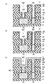
本発明の第1の実施の形態に係わる半導体装置の製造方法は、絶縁膜から放出されるガスを使用して、金属膜と絶縁膜との界面に接する金属膜の表面に酸化物を形成する方法である。
本発明の第2の実施の形態に係わる半導体装置の製造方法は、酸素を固溶する特性をもつ金属膜を、絶縁膜から放出されるガス以外で酸化する方法である。以下に、第2の実施の形態に係る半導体装置の製造方法の例を説明する。以下では、図8に示した層間絶縁膜50上に金属膜30として第2のTi膜30cを形成する場合を例にして説明する。
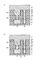
本発明の第3の実施の形態に係る半導体装置の製造方法は、第1の基板温度において、表面に溝、及びビアホールなどの凹部が形成された絶縁膜中、および表面の吸着ガスを放出させる工程と、第1の基板温度より低い第2の基板温度で金属膜を形成する工程と、金属膜上に配線金属膜を少なくとも凹部の一部が埋め込まれていない状態で形成する工程と、第2の基板温度より高い第3の基板温度で加熱して絶縁膜中に残存する酸化種によって、金属膜の少なくとも一部を酸化し、同時に金属膜と配線金属膜の界面で反応層を形成する工程とを含む。
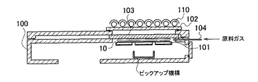
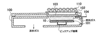
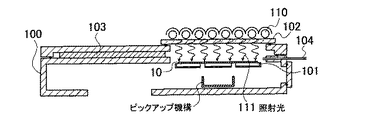
本発明の第4の実施の形態に係る半導体装置の製造方法は、第1の基板温度において、表面に溝、およびビアホールなどの凹部が形成された絶縁膜中、および表面の酸化種吸着ガスを放出させる工程と、第1の基板温度より低い第2の基板温度で、原料ガスを凹部表面に付着させる工程と、凹部表面に付着されなかった残余の原料ガスを排気した後、凹部表面に光を照射して凹部表面に付着した原料ガスの分子を分解し、原料ガスの成分に含まれる金属原子からなる金属膜を、凹部表面に形成する工程とを含む。
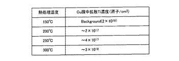
TiCl4(気体) → Ti(固体) + 2Cl2(気体) ・・・(1)
標準生成エンタルピーΔHf°=763kJ/mol ・・・(2)
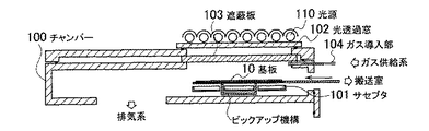
式(1)及び式(2)から、TiCl4の1分子あたりの標準生成エンタルピーは、1.27×10-15Jとなる。TiCl4分子にはTi−Cl結合が4つあるため、1つのTi−Cl結合の結合解離エネルギーは3.17×10-16Jである。Ti−Cl結合の結合解離エネルギーを得るための光の波長は、627nm以下になる。また、TiCl4分子の光吸収波長は、280nmと232nmに極大値を持つ。そのため、627nm以下、且つTiCl4分子の極大吸収波長近傍の波長の光を照射光111として用いれば、TiCl4分子を効率的に分解できる。照射光111をエキシマランプから選択する場合には、Xeエキシマ(波長:172nm)、KrClエキシマ(波長:222nm)、XeClエキシマ(波長:308nm)が選択可能である。又、185nmと254nmの波長の水銀ランプが照射光111として使用可能である。また、狭波長帯の光源の必要はなく、広波長帯の光源を用いてもよい。また、最近の低誘電率絶縁膜は、加熱、電子ビーム照射、UV光照射などによって前駆体をキュア(焼結、重合、あるいは縮合)して形成している。このような低誘電率絶縁膜にさらにUV光を照射した場合、内部の結合しているべき結合手が切れ、場合によっては誘電率の増加を招く場合がある。そのような場合、使用する絶縁膜の性質に合わせて、絶縁膜に影響を及ぼさない波長を選べばよい。特に、UV光照射によるキュア(一般的にはUVキュアと呼ばれる)はエネルギーが一定領域に限られるため、特定、かつ必要な結合手のみの解離を行うことができる。この場合、長時間UV光照射を行なっても、不必要な分解は起こらず、低誘電率絶縁膜の性質は変化しない。従って、第4の実施の形態に用いる光の波長を低誘電率絶縁膜のUVキュアの波長と合わせておけば、絶縁膜にダメージを与えることはない。
一方、脱ガス処理工程より低い温度でTi膜を形成した場合は、図34(b)のように、純Ti膜30aがバリアメタル膜として形成される。つまり、第1の実施の形態で図15を用いて説明したのと同様のメカニズムで、Ti膜30a形成後の絶縁膜形成工程やシンタリング工程などにおいて、分子密度が高いTiOx膜35が形成され(図34(c))、Cu配線のSM耐性が劣化することはない。
本発明の第5の実施の形態に係わる半導体装置の製造方法は、第1から第4の実施の形態で示したCu多層配線に用いられるバリアメタルとしてのTi膜の形成ではなく、メモリー素子のキャパシタンスなどに用いられる高誘電体膜である酸化アルミニウム(Al2O3)膜を形成する方法である。以下に、図27に示した半導体製造装置を用いて、基板上にAl2O3膜を形成する方法を説明する。以下では、トリメチルアルミニウム(TMA;(Al(CH3)3))を原料ガスとして用いる場合を説明する。
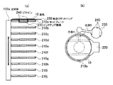
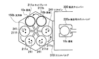
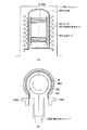
本発明の第6の実施の形態に係る半導体製造装置を図38(a)及び図38(b)に示す。図38(a)及び図38(b)に示す半導体製造装置は、第1〜4の実施の形態で説明した半導体装置の製造方法に適用可能である。
(その他の実施の形態)
上記のように、本発明は第1乃至第6の実施の形態によって記載したが、この開示の一部をなす論述及び図面はこの発明を限定するものであると理解すべきではない。この開示から当業者には様々な代替実施の形態、実施例及び運用技術が明らかとなろう。
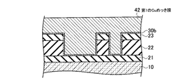
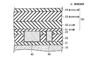
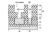
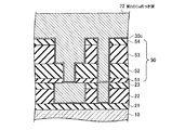
20…絶縁膜
30…金属膜
35…チタン酸化膜
36…タンタル膜
50…層間絶縁膜
70…第2配線層
71…第2のCuシード膜
200…凹部
Claims (5)
- 基板上に絶縁膜、金属からなるバリアメタル膜、及びCu配線金属膜がこの順で積層された積層構造を具備してなり、
前記バリアメタル膜の酸化物のX線回折測定による回折強度が、前記バリアメタル膜と前記Cu配線金属膜との化合物の回折強度の10倍以下であることを特徴とする半導体装置。 - 前記基板と前記絶縁膜の間に配置され、前記絶縁膜に形成されたホール下で前記バリアメタル膜と接続する下層配線層を更に備え、前記下層配線層と接する箇所での前記バリアメタル膜の酸化物中の酸素濃度が、前記絶縁膜と接する箇所の前記バリアメタル膜の酸化物中の酸素濃度より低いことを特徴とする請求項1に記載の半導体装置。
- 前記バリアメタル膜は、Tiからなることを特徴とする請求項1に記載の半導体装置。
- 前記バリアメタル膜と前記絶縁膜との界面近傍に、Tiに対する酸素の原子比が5/3以下である前記バリアメタル膜の酸化物が形成されたことを特徴とする請求項3に記載の半導体装置。
- 請求項1に記載の半導体装置を製造する方法であって、
第1の基板温度で、表面に凹部が形成された前記絶縁膜中及び該絶縁膜表面の酸化を一部残存するように放出させる工程と、
前記酸化種を放出させる工程と真空連続で、前記第1の基板温度より低い、前記絶縁膜中から酸化種が放出されない第2の基板温度で、前記絶縁膜上に、前記バリアメタル膜を形成する工程と、
前記バリアメタル膜上に前記Cu配線金属膜を形成する工程と、
前記バリアメタル膜を形成後、前記絶縁膜中に残存させた酸化種によって、前記バリアメタル膜の少なくとも一部を酸化させる工程と、
前記バリアメタル膜と前記Cu配線金属膜との界面に、前記バリアメタル膜と前記Cu配線金属膜との化合物を形成する工程とを含み、
前記バリアメタル膜を酸化させる工程は、前記バリアメタル膜を前記第1の基板温度よりも高い温度で加熱する工程を含むことを特徴とする半導体装置の製造方法。
Priority Applications (1)
| Application Number | Priority Date | Filing Date | Title |
|---|---|---|---|
| JP2009212140A JP4676015B2 (ja) | 2005-01-21 | 2009-09-14 | 半導体装置 |
Applications Claiming Priority (2)
| Application Number | Priority Date | Filing Date | Title |
|---|---|---|---|
| JP2005014453 | 2005-01-21 | ||
| JP2009212140A JP4676015B2 (ja) | 2005-01-21 | 2009-09-14 | 半導体装置 |
Related Parent Applications (1)
| Application Number | Title | Priority Date | Filing Date |
|---|---|---|---|
| JP2006009978A Division JP4473824B2 (ja) | 2005-01-21 | 2006-01-18 | 半導体装置の製造方法 |
Related Child Applications (1)
| Application Number | Title | Priority Date | Filing Date |
|---|---|---|---|
| JP2010201169A Division JP4734467B2 (ja) | 2005-01-21 | 2010-09-08 | 半導体装置の製造方法 |
Publications (2)
| Publication Number | Publication Date |
|---|---|
| JP2010010700A true JP2010010700A (ja) | 2010-01-14 |
| JP4676015B2 JP4676015B2 (ja) | 2011-04-27 |
Family
ID=37034383
Family Applications (2)
| Application Number | Title | Priority Date | Filing Date |
|---|---|---|---|
| JP2009212140A Active JP4676015B2 (ja) | 2005-01-21 | 2009-09-14 | 半導体装置 |
| JP2010201169A Active JP4734467B2 (ja) | 2005-01-21 | 2010-09-08 | 半導体装置の製造方法 |
Family Applications After (1)
| Application Number | Title | Priority Date | Filing Date |
|---|---|---|---|
| JP2010201169A Active JP4734467B2 (ja) | 2005-01-21 | 2010-09-08 | 半導体装置の製造方法 |
Country Status (3)
| Country | Link |
|---|---|
| US (5) | US7351656B2 (ja) |
| JP (2) | JP4676015B2 (ja) |
| CN (2) | CN100477158C (ja) |
Families Citing this family (39)
| Publication number | Priority date | Publication date | Assignee | Title |
|---|---|---|---|---|
| US7294851B2 (en) * | 2004-11-03 | 2007-11-13 | Infineon Technologies Ag | Dense seed layer and method of formation |
| US7351656B2 (en) * | 2005-01-21 | 2008-04-01 | Kabushiki Kaihsa Toshiba | Semiconductor device having oxidized metal film and manufacture method of the same |
| JP2007234719A (ja) * | 2006-02-28 | 2007-09-13 | Sanyo Electric Co Ltd | 半導体装置およびその製造方法 |
| US7446058B2 (en) * | 2006-05-25 | 2008-11-04 | International Business Machines Corporation | Adhesion enhancement for metal/dielectric interface |
| TW200814156A (en) * | 2006-07-21 | 2008-03-16 | Toshiba Kk | Method for manufacturing semiconductor device and semiconductor device |
| KR100800495B1 (ko) * | 2007-02-27 | 2008-02-04 | 삼성전자주식회사 | 반도체 장치의 제조방법 |
| US20080299780A1 (en) * | 2007-06-01 | 2008-12-04 | Uv Tech Systems, Inc. | Method and apparatus for laser oxidation and reduction |
| KR101412144B1 (ko) * | 2007-11-26 | 2014-06-26 | 삼성전자 주식회사 | 금속 배선의 제조 방법 및 이를 이용한 이미지 센서의 제조방법 |
| JP2009187898A (ja) * | 2008-02-08 | 2009-08-20 | Seiko Epson Corp | 有機el装置及びその製造方法 |
| JP5380901B2 (ja) * | 2008-05-12 | 2014-01-08 | 富士通セミコンダクター株式会社 | 半導体装置及びその製造方法 |
| JP5501586B2 (ja) * | 2008-08-22 | 2014-05-21 | ルネサスエレクトロニクス株式会社 | 半導体装置の製造方法 |
| JP5582727B2 (ja) | 2009-01-19 | 2014-09-03 | 株式会社東芝 | 半導体装置の製造方法及び半導体装置 |
| JP5502339B2 (ja) * | 2009-02-17 | 2014-05-28 | ルネサスエレクトロニクス株式会社 | 半導体装置及び半導体装置の製造方法 |
| JP5025679B2 (ja) * | 2009-03-27 | 2012-09-12 | 株式会社東芝 | 半導体装置 |
| PT104865A (pt) * | 2009-12-09 | 2011-06-09 | Univ Aveiro | Barreira metálica de magnésio contra a difusão de oxigénio aplicada a dispositivos de microelectrónica |
| JP5963456B2 (ja) | 2011-02-18 | 2016-08-03 | 株式会社日立国際電気 | 半導体装置の製造方法、基板処理装置、及び基板処理方法 |
| JP5703105B2 (ja) * | 2011-04-15 | 2015-04-15 | 株式会社東芝 | 半導体装置及びその製造方法 |
| US8853831B2 (en) * | 2012-03-29 | 2014-10-07 | Taiwan Semiconductor Manufacturing Company, Ltd. | Interconnect structure and method for forming the same |
| JP5981206B2 (ja) | 2012-04-20 | 2016-08-31 | 株式会社東芝 | 半導体装置の製造方法および半導体製造装置 |
| US20130307153A1 (en) | 2012-05-18 | 2013-11-21 | International Business Machines Corporation | Interconnect with titanium-oxide diffusion barrier |
| KR101950349B1 (ko) * | 2012-12-26 | 2019-02-20 | 에스케이하이닉스 주식회사 | 보이드 프리 폴리실리콘 갭필 방법 및 그를 이용한 반도체장치 제조 방법 |
| US9136166B2 (en) * | 2013-03-08 | 2015-09-15 | Taiwan Semiconductor Manufacturing Company, Ltd. | Interconnect structure and methods of making same |
| US8802560B1 (en) * | 2013-03-14 | 2014-08-12 | Taiwan Semiconductor Manufacturing Company, Ltd. | Method of fabricating an semiconductor interconnect structure |
| KR102165267B1 (ko) * | 2013-11-18 | 2020-10-13 | 삼성전자 주식회사 | Tsv 구조를 포함하는 집적회로 소자 및 그 제조 방법 |
| US9735134B2 (en) | 2014-03-12 | 2017-08-15 | Taiwan Semiconductor Manufacturing Company, Ltd. | Packages with through-vias having tapered ends |
| US9899325B2 (en) * | 2014-08-07 | 2018-02-20 | Infineon Technologies Ag | Device and method for manufacturing a device with a barrier layer |
| FI126794B (en) | 2014-12-22 | 2017-05-31 | Picosun Oy | Photo-assisted coating process |
| FI126970B (en) * | 2014-12-22 | 2017-08-31 | Picosun Oy | Atomic layer cultivation in which the first and second species of source materials are present simultaneously |
| KR102324826B1 (ko) * | 2015-04-02 | 2021-11-11 | 삼성전자주식회사 | 배선 구조물, 배선 구조물 형성 방법 및 반도체 장치의 제조 방법 |
| KR102389819B1 (ko) * | 2015-06-17 | 2022-04-22 | 삼성전자주식회사 | 반도체 소자의 제조 방법 |
| KR102491577B1 (ko) * | 2015-09-23 | 2023-01-25 | 삼성전자주식회사 | 유전 층을 갖는 반도체 소자 형성 방법 및 관련된 시스템 |
| US9536780B1 (en) * | 2016-04-15 | 2017-01-03 | International Business Machines Corporation | Method and apparatus for single chamber treatment |
| US9831174B1 (en) * | 2016-05-31 | 2017-11-28 | Globalfoundries Inc. | Devices and methods of forming low resistivity noble metal interconnect |
| JP6868455B2 (ja) | 2016-06-02 | 2021-05-12 | パナソニック株式会社 | 電子部品パッケージおよびその製造方法 |
| JP6865632B2 (ja) * | 2017-05-09 | 2021-04-28 | 東京エレクトロン株式会社 | 基板洗浄装置および基板洗浄方法 |
| JP2019062142A (ja) * | 2017-09-28 | 2019-04-18 | 東京エレクトロン株式会社 | 選択成膜方法および半導体装置の製造方法 |
| US10727118B2 (en) * | 2017-11-30 | 2020-07-28 | Taiwan Semiconductor Manufacturing Co., Ltd. | Method for manufacturing semiconductor device and pre-clean apparatus for semiconductor device |
| JP7321730B2 (ja) * | 2019-03-14 | 2023-08-07 | キオクシア株式会社 | 半導体装置の製造方法 |
| US11380536B2 (en) * | 2020-05-05 | 2022-07-05 | Applied Materials, Inc. | Multi-step pre-clean for selective metal gap fill |
Citations (1)
| Publication number | Priority date | Publication date | Assignee | Title |
|---|---|---|---|---|
| JP2000124307A (ja) * | 1998-10-19 | 2000-04-28 | Sony Corp | 金属系膜の形成方法および電子装置の製造方法 |
Family Cites Families (57)
| Publication number | Priority date | Publication date | Assignee | Title |
|---|---|---|---|---|
| US4062318A (en) * | 1976-11-19 | 1977-12-13 | Rca Corporation | Apparatus for chemical vapor deposition |
| US4295896A (en) * | 1979-03-12 | 1981-10-20 | Massachusetts Institute Of Technology | Method for making metal alloy compositions and composition |
| US5259881A (en) * | 1991-05-17 | 1993-11-09 | Materials Research Corporation | Wafer processing cluster tool batch preheating and degassing apparatus |
| JPS62104438U (ja) * | 1985-12-23 | 1987-07-03 | ||
| US4855160A (en) * | 1987-07-16 | 1989-08-08 | Texas Instruments Incorporated | Method for passivating wafer |
| US5215588A (en) | 1992-01-17 | 1993-06-01 | Amtech Systems, Inc. | Photo-CVD system |
| US5404894A (en) * | 1992-05-20 | 1995-04-11 | Tokyo Electron Kabushiki Kaisha | Conveyor apparatus |
| US5697749A (en) * | 1992-07-17 | 1997-12-16 | Tokyo Electron Kabushiki Kaisha | Wafer processing apparatus |
| KR970001883B1 (ko) * | 1992-12-30 | 1997-02-18 | 삼성전자 주식회사 | 반도체장치 및 그 제조방법 |
| US6090701A (en) * | 1994-06-21 | 2000-07-18 | Kabushiki Kaisha Toshiba | Method for production of semiconductor device |
| CN1107979C (zh) * | 1995-07-14 | 2003-05-07 | 松下电器产业株式会社 | 半导体器件的电极结构、形成方法及安装体和半导体器件 |
| JP3947761B2 (ja) * | 1996-09-26 | 2007-07-25 | 株式会社日立国際電気 | 基板処理装置、基板搬送機および基板処理方法 |
| JPH10125782A (ja) | 1996-10-15 | 1998-05-15 | Sony Corp | 半導体装置の製造方法 |
| US5855681A (en) * | 1996-11-18 | 1999-01-05 | Applied Materials, Inc. | Ultra high throughput wafer vacuum processing system |
| JPH10223900A (ja) * | 1996-12-03 | 1998-08-21 | Toshiba Corp | 半導体装置及び半導体装置の製造方法 |
| NL1005102C2 (nl) * | 1997-01-27 | 1998-07-29 | Advanced Semiconductor Mat | Inrichting voor het behandelen van halfgeleiderschijven. |
| JPH10233444A (ja) * | 1997-02-19 | 1998-09-02 | Mitsubishi Electric Corp | 半導体装置の製造方法 |
| JPH10242274A (ja) * | 1997-02-27 | 1998-09-11 | Sony Corp | 多層配線基板の製造方法 |
| JPH10256372A (ja) | 1997-03-17 | 1998-09-25 | Sony Corp | 半導体装置の製造方法 |
| CH692741A5 (de) * | 1997-07-08 | 2002-10-15 | Unaxis Trading Ltd C O Balzers | Verfahren zur Herstellung in Vakuum oberflächenbehandelter Werkstücke und Vakuumbehandlungsanlage zu dessen Durchführung |
| TW589391B (en) * | 1997-07-08 | 2004-06-01 | Unaxis Trading Ag | Process for vacuum treating workpieces, and corresponding process equipment |
| US20030049372A1 (en) * | 1997-08-11 | 2003-03-13 | Cook Robert C. | High rate deposition at low pressures in a small batch reactor |
| JP3329290B2 (ja) * | 1998-11-27 | 2002-09-30 | 日本電気株式会社 | 半導体装置の製造方法 |
| JP4008664B2 (ja) * | 1998-12-16 | 2007-11-14 | 東京エレクトロン株式会社 | 薄膜形成方法 |
| US6204178B1 (en) * | 1998-12-29 | 2001-03-20 | Micron Technology, Inc. | Nucleation and deposition of PT films using ultraviolet irradiation |
| JP3974284B2 (ja) * | 1999-03-18 | 2007-09-12 | 株式会社東芝 | 半導体装置の製造方法 |
| JP4021601B2 (ja) * | 1999-10-29 | 2007-12-12 | 株式会社東芝 | スパッタ装置および成膜方法 |
| US6136702A (en) | 1999-11-29 | 2000-10-24 | Lucent Technologies Inc. | Thin film transistors |
| JP2001196453A (ja) | 2000-01-14 | 2001-07-19 | Seiko Epson Corp | 半導体装置及びその製造方法 |
| JP4776054B2 (ja) | 2000-02-04 | 2011-09-21 | 株式会社デンソー | 原子層成長による薄膜形成方法 |
| JP3651765B2 (ja) * | 2000-03-27 | 2005-05-25 | 株式会社東芝 | 半導体装置 |
| US7060132B2 (en) * | 2000-04-14 | 2006-06-13 | Asm International N.V. | Method and apparatus of growing a thin film |
| JP2001338988A (ja) | 2000-05-25 | 2001-12-07 | Hitachi Ltd | 半導体装置及びその製造方法 |
| JP2002170821A (ja) | 2000-11-30 | 2002-06-14 | Sony Corp | 膜の形成方法 |
| JP3643533B2 (ja) * | 2000-12-27 | 2005-04-27 | 株式会社東芝 | 半導体装置およびその製造方法 |
| US7014709B1 (en) * | 2001-01-19 | 2006-03-21 | Novellus Systems, Inc. | Thin layer metal chemical vapor deposition |
| JP4696373B2 (ja) * | 2001-02-20 | 2011-06-08 | 東京エレクトロン株式会社 | 処理システム及び被処理体の搬送方法 |
| KR100396891B1 (ko) * | 2001-03-21 | 2003-09-03 | 삼성전자주식회사 | 반도체 소자의 금속 배선 형성 방법 |
| US20040173948A1 (en) * | 2002-09-19 | 2004-09-09 | Pandelisev Kiril A. | Process and apparatus for silicon boat, silicon tubing and other silicon based member fabrication |
| JP3648480B2 (ja) * | 2001-12-26 | 2005-05-18 | 株式会社東芝 | 半導体装置およびその製造方法 |
| JP3937892B2 (ja) | 2002-04-01 | 2007-06-27 | 日本電気株式会社 | 薄膜形成方法および半導体装置の製造方法 |
| US7018268B2 (en) * | 2002-04-09 | 2006-03-28 | Strasbaugh | Protection of work piece during surface processing |
| JP4285946B2 (ja) | 2002-06-06 | 2009-06-24 | 株式会社ルネサステクノロジ | 半導体装置の製造方法 |
| KR100497748B1 (ko) * | 2002-09-17 | 2005-06-29 | 주식회사 무한 | 반도체소자 제조용 원자층 증착 장치 및 원자층 증착 방법 |
| JP2004119754A (ja) * | 2002-09-27 | 2004-04-15 | Seiko Epson Corp | 配線、配線の製造方法、半導体装置及びその製造方法 |
| JP2004134617A (ja) * | 2002-10-11 | 2004-04-30 | Seiko Epson Corp | 配線の製造方法、半導体装置及びその製造方法 |
| KR100483594B1 (ko) * | 2002-12-27 | 2005-04-15 | 매그나칩 반도체 유한회사 | 반도체 소자의 금속배선 형성방법 |
| JP2004296620A (ja) * | 2003-03-26 | 2004-10-21 | Nec Electronics Corp | 半導体装置の製造方法 |
| US6972055B2 (en) * | 2003-03-28 | 2005-12-06 | Finens Corporation | Continuous flow deposition system |
| JP4219215B2 (ja) * | 2003-05-30 | 2009-02-04 | 株式会社ルネサステクノロジ | 電子デバイスの製造方法 |
| KR100555543B1 (ko) | 2003-06-24 | 2006-03-03 | 삼성전자주식회사 | 원자층 증착법에 의한 고유전막 형성 방법 및 그고유전막을 갖는 커패시터의 제조 방법 |
| US20060137609A1 (en) * | 2004-09-13 | 2006-06-29 | Puchacz Jerzy P | Multi-single wafer processing apparatus |
| US7335980B2 (en) * | 2004-11-04 | 2008-02-26 | International Business Machines Corporation | Hardmask for reliability of silicon based dielectrics |
| WO2006055984A2 (en) * | 2004-11-22 | 2006-05-26 | Applied Materials, Inc. | Substrate processing apparatus using a batch processing chamber |
| US7351656B2 (en) | 2005-01-21 | 2008-04-01 | Kabushiki Kaihsa Toshiba | Semiconductor device having oxidized metal film and manufacture method of the same |
| US20080257260A9 (en) * | 2005-09-30 | 2008-10-23 | Applied Materials, Inc. | Batch wafer handling system |
| US20120272892A1 (en) * | 2011-04-07 | 2012-11-01 | Veeco Instruments Inc. | Metal-Organic Vapor Phase Epitaxy System and Process |
-
2006
- 2006-01-20 US US11/335,584 patent/US7351656B2/en active Active
- 2006-01-23 CN CNB2006100739216A patent/CN100477158C/zh active Active
- 2006-01-23 CN CN2008101256289A patent/CN101350340B/zh active Active
-
2007
- 2007-08-30 US US11/896,271 patent/US7994054B2/en active Active
-
2008
- 2008-01-24 US US12/010,371 patent/US7791202B2/en active Active
- 2008-01-24 US US12/010,372 patent/US8148274B2/en active Active
-
2009
- 2009-09-14 JP JP2009212140A patent/JP4676015B2/ja active Active
-
2010
- 2010-09-08 JP JP2010201169A patent/JP4734467B2/ja active Active
-
2012
- 2012-02-29 US US13/407,802 patent/US20120152168A1/en not_active Abandoned
Patent Citations (1)
| Publication number | Priority date | Publication date | Assignee | Title |
|---|---|---|---|---|
| JP2000124307A (ja) * | 1998-10-19 | 2000-04-28 | Sony Corp | 金属系膜の形成方法および電子装置の製造方法 |
Also Published As
| Publication number | Publication date |
|---|---|
| CN101350340A (zh) | 2009-01-21 |
| CN1848407A (zh) | 2006-10-18 |
| US7994054B2 (en) | 2011-08-09 |
| US7351656B2 (en) | 2008-04-01 |
| JP4676015B2 (ja) | 2011-04-27 |
| US20080261398A1 (en) | 2008-10-23 |
| US20080090410A1 (en) | 2008-04-17 |
| US8148274B2 (en) | 2012-04-03 |
| US20120152168A1 (en) | 2012-06-21 |
| US20060214305A1 (en) | 2006-09-28 |
| CN100477158C (zh) | 2009-04-08 |
| US20080122102A1 (en) | 2008-05-29 |
| JP2010272898A (ja) | 2010-12-02 |
| CN101350340B (zh) | 2013-09-18 |
| US7791202B2 (en) | 2010-09-07 |
| JP4734467B2 (ja) | 2011-07-27 |
Similar Documents
| Publication | Publication Date | Title |
|---|---|---|
| JP4734467B2 (ja) | 半導体装置の製造方法 | |
| JP4473824B2 (ja) | 半導体装置の製造方法 | |
| JP5674669B2 (ja) | ルテニウム金属キャップ層を形成する方法 | |
| KR101178650B1 (ko) | 반도체 장치의 제조 방법, 반도체 장치, 전자 기기, 반도체 제조 장치 및 기억 매체 | |
| US8242015B2 (en) | Film forming method and film forming apparatus | |
| JP5522979B2 (ja) | 成膜方法及び処理システム | |
| KR101739613B1 (ko) | Cu 배선의 형성 방법 | |
| WO2012133400A1 (ja) | Cu配線の形成方法 | |
| TW201043721A (en) | Method for forming cvd-ru film and method for manufacturing semiconductor devices | |
| KR101662369B1 (ko) | Cu 배선의 형성 방법 및 기억매체 | |
| KR20140143095A (ko) | 산화 망간막의 형성 방법 | |
| JP2008140998A (ja) | 成膜方法、成膜装置及び記憶媒体、並びに半導体装置 | |
| JP4931171B2 (ja) | タンタル窒化物膜の形成方法 | |
| KR20170026165A (ko) | 반도체 장치의 제조 방법 및 기억 매체 | |
| KR20180117575A (ko) | Cu 배선의 제조 방법 및 Cu 배선 제조 시스템 | |
| US20020157610A1 (en) | Method for forming a copper thin film | |
| JP2006024668A (ja) | 半導体装置の製造方法 | |
| JP2006147895A (ja) | 半導体装置の製造方法 | |
| Liu | Plasma surface interactions at interlayer dielectric (ILD) and metal surfaces |
Legal Events
| Date | Code | Title | Description |
|---|---|---|---|
| A131 | Notification of reasons for refusal |
Free format text: JAPANESE INTERMEDIATE CODE: A131 Effective date: 20100209 |
|
| A521 | Request for written amendment filed |
Free format text: JAPANESE INTERMEDIATE CODE: A523 Effective date: 20100408 |
|
| A02 | Decision of refusal |
Free format text: JAPANESE INTERMEDIATE CODE: A02 Effective date: 20100608 |
|
| A521 | Request for written amendment filed |
Free format text: JAPANESE INTERMEDIATE CODE: A523 Effective date: 20100908 |
|
| A911 | Transfer to examiner for re-examination before appeal (zenchi) |
Free format text: JAPANESE INTERMEDIATE CODE: A911 Effective date: 20101026 |
|
| TRDD | Decision of grant or rejection written | ||
| A01 | Written decision to grant a patent or to grant a registration (utility model) |
Free format text: JAPANESE INTERMEDIATE CODE: A01 Effective date: 20110104 |
|
| A01 | Written decision to grant a patent or to grant a registration (utility model) |
Free format text: JAPANESE INTERMEDIATE CODE: A01 |
|
| A61 | First payment of annual fees (during grant procedure) |
Free format text: JAPANESE INTERMEDIATE CODE: A61 Effective date: 20110126 |
|
| FPAY | Renewal fee payment (event date is renewal date of database) |
Free format text: PAYMENT UNTIL: 20140204 Year of fee payment: 3 |
|
| R151 | Written notification of patent or utility model registration |
Ref document number: 4676015 Country of ref document: JP Free format text: JAPANESE INTERMEDIATE CODE: R151 |
|
| FPAY | Renewal fee payment (event date is renewal date of database) |
Free format text: PAYMENT UNTIL: 20140204 Year of fee payment: 3 |
|
| S111 | Request for change of ownership or part of ownership |
Free format text: JAPANESE INTERMEDIATE CODE: R313111 |
|
| R350 | Written notification of registration of transfer |
Free format text: JAPANESE INTERMEDIATE CODE: R350 |
|
| S111 | Request for change of ownership or part of ownership |
Free format text: JAPANESE INTERMEDIATE CODE: R313111 |
|
| R350 | Written notification of registration of transfer |
Free format text: JAPANESE INTERMEDIATE CODE: R350 |