JP2007123797A - 半導体ic内蔵基板及びその製造方法 - Google Patents

半導体ic内蔵基板及びその製造方法 Download PDF

Info

Publication number
JP2007123797A
JP2007123797A JP2006050475A JP2006050475A JP2007123797A JP 2007123797 A JP2007123797 A JP 2007123797A JP 2006050475 A JP2006050475 A JP 2006050475A JP 2006050475 A JP2006050475 A JP 2006050475A JP 2007123797 A JP2007123797 A JP 2007123797A
Authority
JP
Japan
Prior art keywords
semiconductor
resin layer
substrate
built
wiring pattern
Prior art date
Legal status (The legal status is an assumption and is not a legal conclusion. Google has not performed a legal analysis and makes no representation as to the accuracy of the status listed.)
Granted
Application number
JP2006050475A
Other languages
English (en)
Other versions
JP4535002B2 (ja
Inventor
Kenichi Kawabata
賢一 川畑
Takaaki Morita
高章 森田
Current Assignee (The listed assignees may be inaccurate. Google has not performed a legal analysis and makes no representation or warranty as to the accuracy of the list.)
TDK Corp
Original Assignee
TDK Corp
Priority date (The priority date is an assumption and is not a legal conclusion. Google has not performed a legal analysis and makes no representation as to the accuracy of the date listed.)
Filing date
Publication date
Application filed by TDK Corp filed Critical TDK Corp
Priority to JP2006050475A priority Critical patent/JP4535002B2/ja
Priority to EP06254920.9A priority patent/EP1770776B1/en
Priority to TW095135324A priority patent/TW200721419A/zh
Priority to US11/527,829 priority patent/US7544537B2/en
Priority to CN2006101599557A priority patent/CN1941339B/zh
Priority to KR1020060094814A priority patent/KR101176814B1/ko
Publication of JP2007123797A publication Critical patent/JP2007123797A/ja
Priority to US12/435,385 priority patent/US8026614B2/en
Application granted granted Critical
Publication of JP4535002B2 publication Critical patent/JP4535002B2/ja
Active legal-status Critical Current
Anticipated expiration legal-status Critical

Links

Images

Classifications

    • HELECTRICITY
    • H01ELECTRIC ELEMENTS
    • H01LSEMICONDUCTOR DEVICES NOT COVERED BY CLASS H10
    • H01L23/00Details of semiconductor or other solid state devices
    • H01L23/52Arrangements for conducting electric current within the device in operation from one component to another, i.e. interconnections, e.g. wires, lead frames
    • H01L23/538Arrangements for conducting electric current within the device in operation from one component to another, i.e. interconnections, e.g. wires, lead frames the interconnection structure between a plurality of semiconductor chips being formed on, or in, insulating substrates
    • H01L23/5389Arrangements for conducting electric current within the device in operation from one component to another, i.e. interconnections, e.g. wires, lead frames the interconnection structure between a plurality of semiconductor chips being formed on, or in, insulating substrates the chips being integrally enclosed by the interconnect and support structures
    • HELECTRICITY
    • H01ELECTRIC ELEMENTS
    • H01LSEMICONDUCTOR DEVICES NOT COVERED BY CLASS H10
    • H01L23/00Details of semiconductor or other solid state devices
    • H01L23/12Mountings, e.g. non-detachable insulating substrates
    • HELECTRICITY
    • H01ELECTRIC ELEMENTS
    • H01LSEMICONDUCTOR DEVICES NOT COVERED BY CLASS H10
    • H01L21/00Processes or apparatus adapted for the manufacture or treatment of semiconductor or solid state devices or of parts thereof
    • H01L21/02Manufacture or treatment of semiconductor devices or of parts thereof
    • H01L21/04Manufacture or treatment of semiconductor devices or of parts thereof the devices having at least one potential-jump barrier or surface barrier, e.g. PN junction, depletion layer or carrier concentration layer
    • H01L21/50Assembly of semiconductor devices using processes or apparatus not provided for in a single one of the subgroups H01L21/06 - H01L21/326, e.g. sealing of a cap to a base of a container
    • H01L21/56Encapsulations, e.g. encapsulation layers, coatings
    • H01L21/568Temporary substrate used as encapsulation process aid
    • HELECTRICITY
    • H01ELECTRIC ELEMENTS
    • H01LSEMICONDUCTOR DEVICES NOT COVERED BY CLASS H10
    • H01L21/00Processes or apparatus adapted for the manufacture or treatment of semiconductor or solid state devices or of parts thereof
    • H01L21/67Apparatus specially adapted for handling semiconductor or electric solid state devices during manufacture or treatment thereof; Apparatus specially adapted for handling wafers during manufacture or treatment of semiconductor or electric solid state devices or components ; Apparatus not specifically provided for elsewhere
    • H01L21/683Apparatus specially adapted for handling semiconductor or electric solid state devices during manufacture or treatment thereof; Apparatus specially adapted for handling wafers during manufacture or treatment of semiconductor or electric solid state devices or components ; Apparatus not specifically provided for elsewhere for supporting or gripping
    • H01L21/6835Apparatus specially adapted for handling semiconductor or electric solid state devices during manufacture or treatment thereof; Apparatus specially adapted for handling wafers during manufacture or treatment of semiconductor or electric solid state devices or components ; Apparatus not specifically provided for elsewhere for supporting or gripping using temporarily an auxiliary support
    • HELECTRICITY
    • H01ELECTRIC ELEMENTS
    • H01LSEMICONDUCTOR DEVICES NOT COVERED BY CLASS H10
    • H01L23/00Details of semiconductor or other solid state devices
    • H01L23/52Arrangements for conducting electric current within the device in operation from one component to another, i.e. interconnections, e.g. wires, lead frames
    • H01L23/538Arrangements for conducting electric current within the device in operation from one component to another, i.e. interconnections, e.g. wires, lead frames the interconnection structure between a plurality of semiconductor chips being formed on, or in, insulating substrates
    • H01L23/5383Multilayer substrates
    • HELECTRICITY
    • H01ELECTRIC ELEMENTS
    • H01LSEMICONDUCTOR DEVICES NOT COVERED BY CLASS H10
    • H01L23/00Details of semiconductor or other solid state devices
    • H01L23/52Arrangements for conducting electric current within the device in operation from one component to another, i.e. interconnections, e.g. wires, lead frames
    • H01L23/538Arrangements for conducting electric current within the device in operation from one component to another, i.e. interconnections, e.g. wires, lead frames the interconnection structure between a plurality of semiconductor chips being formed on, or in, insulating substrates
    • H01L23/5384Conductive vias through the substrate with or without pins, e.g. buried coaxial conductors
    • HELECTRICITY
    • H01ELECTRIC ELEMENTS
    • H01LSEMICONDUCTOR DEVICES NOT COVERED BY CLASS H10
    • H01L23/00Details of semiconductor or other solid state devices
    • H01L23/544Marks applied to semiconductor devices or parts, e.g. registration marks, alignment structures, wafer maps
    • HELECTRICITY
    • H01ELECTRIC ELEMENTS
    • H01LSEMICONDUCTOR DEVICES NOT COVERED BY CLASS H10
    • H01L24/00Arrangements for connecting or disconnecting semiconductor or solid-state bodies; Methods or apparatus related thereto
    • H01L24/01Means for bonding being attached to, or being formed on, the surface to be connected, e.g. chip-to-package, die-attach, "first-level" interconnects; Manufacturing methods related thereto
    • H01L24/18High density interconnect [HDI] connectors; Manufacturing methods related thereto
    • H01L24/23Structure, shape, material or disposition of the high density interconnect connectors after the connecting process
    • H01L24/24Structure, shape, material or disposition of the high density interconnect connectors after the connecting process of an individual high density interconnect connector
    • HELECTRICITY
    • H01ELECTRIC ELEMENTS
    • H01LSEMICONDUCTOR DEVICES NOT COVERED BY CLASS H10
    • H01L24/00Arrangements for connecting or disconnecting semiconductor or solid-state bodies; Methods or apparatus related thereto
    • H01L24/01Means for bonding being attached to, or being formed on, the surface to be connected, e.g. chip-to-package, die-attach, "first-level" interconnects; Manufacturing methods related thereto
    • H01L24/18High density interconnect [HDI] connectors; Manufacturing methods related thereto
    • H01L24/23Structure, shape, material or disposition of the high density interconnect connectors after the connecting process
    • H01L24/25Structure, shape, material or disposition of the high density interconnect connectors after the connecting process of a plurality of high density interconnect connectors
    • HELECTRICITY
    • H01ELECTRIC ELEMENTS
    • H01LSEMICONDUCTOR DEVICES NOT COVERED BY CLASS H10
    • H01L24/00Arrangements for connecting or disconnecting semiconductor or solid-state bodies; Methods or apparatus related thereto
    • H01L24/80Methods for connecting semiconductor or other solid state bodies using means for bonding being attached to, or being formed on, the surface to be connected
    • H01L24/82Methods for connecting semiconductor or other solid state bodies using means for bonding being attached to, or being formed on, the surface to be connected by forming build-up interconnects at chip-level, e.g. for high density interconnects [HDI]
    • HELECTRICITY
    • H05ELECTRIC TECHNIQUES NOT OTHERWISE PROVIDED FOR
    • H05KPRINTED CIRCUITS; CASINGS OR CONSTRUCTIONAL DETAILS OF ELECTRIC APPARATUS; MANUFACTURE OF ASSEMBLAGES OF ELECTRICAL COMPONENTS
    • H05K1/00Printed circuits
    • H05K1/18Printed circuits structurally associated with non-printed electric components
    • H05K1/182Printed circuits structurally associated with non-printed electric components associated with components mounted in the printed circuit board, e.g. insert mounted components [IMC]
    • H05K1/185Components encapsulated in the insulating substrate of the printed circuit or incorporated in internal layers of a multilayer circuit
    • HELECTRICITY
    • H01ELECTRIC ELEMENTS
    • H01LSEMICONDUCTOR DEVICES NOT COVERED BY CLASS H10
    • H01L2221/00Processes or apparatus adapted for the manufacture or treatment of semiconductor or solid state devices or of parts thereof covered by H01L21/00
    • H01L2221/67Apparatus for handling semiconductor or electric solid state devices during manufacture or treatment thereof; Apparatus for handling wafers during manufacture or treatment of semiconductor or electric solid state devices or components; Apparatus not specifically provided for elsewhere
    • H01L2221/683Apparatus for handling semiconductor or electric solid state devices during manufacture or treatment thereof; Apparatus for handling wafers during manufacture or treatment of semiconductor or electric solid state devices or components; Apparatus not specifically provided for elsewhere for supporting or gripping
    • H01L2221/68304Apparatus for handling semiconductor or electric solid state devices during manufacture or treatment thereof; Apparatus for handling wafers during manufacture or treatment of semiconductor or electric solid state devices or components; Apparatus not specifically provided for elsewhere for supporting or gripping using temporarily an auxiliary support
    • H01L2221/68368Apparatus for handling semiconductor or electric solid state devices during manufacture or treatment thereof; Apparatus for handling wafers during manufacture or treatment of semiconductor or electric solid state devices or components; Apparatus not specifically provided for elsewhere for supporting or gripping using temporarily an auxiliary support used in a transfer process involving at least two transfer steps, i.e. including an intermediate handle substrate
    • HELECTRICITY
    • H01ELECTRIC ELEMENTS
    • H01LSEMICONDUCTOR DEVICES NOT COVERED BY CLASS H10
    • H01L2223/00Details relating to semiconductor or other solid state devices covered by the group H01L23/00
    • H01L2223/544Marks applied to semiconductor devices or parts
    • H01L2223/54473Marks applied to semiconductor devices or parts for use after dicing
    • HELECTRICITY
    • H01ELECTRIC ELEMENTS
    • H01LSEMICONDUCTOR DEVICES NOT COVERED BY CLASS H10
    • H01L2224/00Indexing scheme for arrangements for connecting or disconnecting semiconductor or solid-state bodies and methods related thereto as covered by H01L24/00
    • H01L2224/01Means for bonding being attached to, or being formed on, the surface to be connected, e.g. chip-to-package, die-attach, "first-level" interconnects; Manufacturing methods related thereto
    • H01L2224/02Bonding areas; Manufacturing methods related thereto
    • H01L2224/04Structure, shape, material or disposition of the bonding areas prior to the connecting process
    • H01L2224/0401Bonding areas specifically adapted for bump connectors, e.g. under bump metallisation [UBM]
    • HELECTRICITY
    • H01ELECTRIC ELEMENTS
    • H01LSEMICONDUCTOR DEVICES NOT COVERED BY CLASS H10
    • H01L2224/00Indexing scheme for arrangements for connecting or disconnecting semiconductor or solid-state bodies and methods related thereto as covered by H01L24/00
    • H01L2224/01Means for bonding being attached to, or being formed on, the surface to be connected, e.g. chip-to-package, die-attach, "first-level" interconnects; Manufacturing methods related thereto
    • H01L2224/02Bonding areas; Manufacturing methods related thereto
    • H01L2224/04Structure, shape, material or disposition of the bonding areas prior to the connecting process
    • H01L2224/04105Bonding areas formed on an encapsulation of the semiconductor or solid-state body, e.g. bonding areas on chip-scale packages
    • HELECTRICITY
    • H01ELECTRIC ELEMENTS
    • H01LSEMICONDUCTOR DEVICES NOT COVERED BY CLASS H10
    • H01L2224/00Indexing scheme for arrangements for connecting or disconnecting semiconductor or solid-state bodies and methods related thereto as covered by H01L24/00
    • H01L2224/01Means for bonding being attached to, or being formed on, the surface to be connected, e.g. chip-to-package, die-attach, "first-level" interconnects; Manufacturing methods related thereto
    • H01L2224/10Bump connectors; Manufacturing methods related thereto
    • H01L2224/11Manufacturing methods
    • H01L2224/113Manufacturing methods by local deposition of the material of the bump connector
    • H01L2224/1133Manufacturing methods by local deposition of the material of the bump connector in solid form
    • H01L2224/1134Stud bumping, i.e. using a wire-bonding apparatus
    • HELECTRICITY
    • H01ELECTRIC ELEMENTS
    • H01LSEMICONDUCTOR DEVICES NOT COVERED BY CLASS H10
    • H01L2224/00Indexing scheme for arrangements for connecting or disconnecting semiconductor or solid-state bodies and methods related thereto as covered by H01L24/00
    • H01L2224/01Means for bonding being attached to, or being formed on, the surface to be connected, e.g. chip-to-package, die-attach, "first-level" interconnects; Manufacturing methods related thereto
    • H01L2224/10Bump connectors; Manufacturing methods related thereto
    • H01L2224/12Structure, shape, material or disposition of the bump connectors prior to the connecting process
    • H01L2224/13Structure, shape, material or disposition of the bump connectors prior to the connecting process of an individual bump connector
    • H01L2224/13001Core members of the bump connector
    • H01L2224/13099Material
    • H01L2224/131Material with a principal constituent of the material being a metal or a metalloid, e.g. boron [B], silicon [Si], germanium [Ge], arsenic [As], antimony [Sb], tellurium [Te] and polonium [Po], and alloys thereof
    • H01L2224/13101Material with a principal constituent of the material being a metal or a metalloid, e.g. boron [B], silicon [Si], germanium [Ge], arsenic [As], antimony [Sb], tellurium [Te] and polonium [Po], and alloys thereof the principal constituent melting at a temperature of less than 400°C
    • H01L2224/13111Tin [Sn] as principal constituent
    • HELECTRICITY
    • H01ELECTRIC ELEMENTS
    • H01LSEMICONDUCTOR DEVICES NOT COVERED BY CLASS H10
    • H01L2224/00Indexing scheme for arrangements for connecting or disconnecting semiconductor or solid-state bodies and methods related thereto as covered by H01L24/00
    • H01L2224/01Means for bonding being attached to, or being formed on, the surface to be connected, e.g. chip-to-package, die-attach, "first-level" interconnects; Manufacturing methods related thereto
    • H01L2224/10Bump connectors; Manufacturing methods related thereto
    • H01L2224/12Structure, shape, material or disposition of the bump connectors prior to the connecting process
    • H01L2224/13Structure, shape, material or disposition of the bump connectors prior to the connecting process of an individual bump connector
    • H01L2224/13001Core members of the bump connector
    • H01L2224/13099Material
    • H01L2224/131Material with a principal constituent of the material being a metal or a metalloid, e.g. boron [B], silicon [Si], germanium [Ge], arsenic [As], antimony [Sb], tellurium [Te] and polonium [Po], and alloys thereof
    • H01L2224/13138Material with a principal constituent of the material being a metal or a metalloid, e.g. boron [B], silicon [Si], germanium [Ge], arsenic [As], antimony [Sb], tellurium [Te] and polonium [Po], and alloys thereof the principal constituent melting at a temperature of greater than or equal to 950°C and less than 1550°C
    • H01L2224/13139Silver [Ag] as principal constituent
    • HELECTRICITY
    • H01ELECTRIC ELEMENTS
    • H01LSEMICONDUCTOR DEVICES NOT COVERED BY CLASS H10
    • H01L2224/00Indexing scheme for arrangements for connecting or disconnecting semiconductor or solid-state bodies and methods related thereto as covered by H01L24/00
    • H01L2224/01Means for bonding being attached to, or being formed on, the surface to be connected, e.g. chip-to-package, die-attach, "first-level" interconnects; Manufacturing methods related thereto
    • H01L2224/10Bump connectors; Manufacturing methods related thereto
    • H01L2224/12Structure, shape, material or disposition of the bump connectors prior to the connecting process
    • H01L2224/13Structure, shape, material or disposition of the bump connectors prior to the connecting process of an individual bump connector
    • H01L2224/13001Core members of the bump connector
    • H01L2224/13099Material
    • H01L2224/131Material with a principal constituent of the material being a metal or a metalloid, e.g. boron [B], silicon [Si], germanium [Ge], arsenic [As], antimony [Sb], tellurium [Te] and polonium [Po], and alloys thereof
    • H01L2224/13138Material with a principal constituent of the material being a metal or a metalloid, e.g. boron [B], silicon [Si], germanium [Ge], arsenic [As], antimony [Sb], tellurium [Te] and polonium [Po], and alloys thereof the principal constituent melting at a temperature of greater than or equal to 950°C and less than 1550°C
    • H01L2224/13144Gold [Au] as principal constituent
    • HELECTRICITY
    • H01ELECTRIC ELEMENTS
    • H01LSEMICONDUCTOR DEVICES NOT COVERED BY CLASS H10
    • H01L2224/00Indexing scheme for arrangements for connecting or disconnecting semiconductor or solid-state bodies and methods related thereto as covered by H01L24/00
    • H01L2224/01Means for bonding being attached to, or being formed on, the surface to be connected, e.g. chip-to-package, die-attach, "first-level" interconnects; Manufacturing methods related thereto
    • H01L2224/10Bump connectors; Manufacturing methods related thereto
    • H01L2224/12Structure, shape, material or disposition of the bump connectors prior to the connecting process
    • H01L2224/13Structure, shape, material or disposition of the bump connectors prior to the connecting process of an individual bump connector
    • H01L2224/13001Core members of the bump connector
    • H01L2224/13099Material
    • H01L2224/131Material with a principal constituent of the material being a metal or a metalloid, e.g. boron [B], silicon [Si], germanium [Ge], arsenic [As], antimony [Sb], tellurium [Te] and polonium [Po], and alloys thereof
    • H01L2224/13138Material with a principal constituent of the material being a metal or a metalloid, e.g. boron [B], silicon [Si], germanium [Ge], arsenic [As], antimony [Sb], tellurium [Te] and polonium [Po], and alloys thereof the principal constituent melting at a temperature of greater than or equal to 950°C and less than 1550°C
    • H01L2224/13147Copper [Cu] as principal constituent
    • HELECTRICITY
    • H01ELECTRIC ELEMENTS
    • H01LSEMICONDUCTOR DEVICES NOT COVERED BY CLASS H10
    • H01L2224/00Indexing scheme for arrangements for connecting or disconnecting semiconductor or solid-state bodies and methods related thereto as covered by H01L24/00
    • H01L2224/01Means for bonding being attached to, or being formed on, the surface to be connected, e.g. chip-to-package, die-attach, "first-level" interconnects; Manufacturing methods related thereto
    • H01L2224/10Bump connectors; Manufacturing methods related thereto
    • H01L2224/12Structure, shape, material or disposition of the bump connectors prior to the connecting process
    • H01L2224/13Structure, shape, material or disposition of the bump connectors prior to the connecting process of an individual bump connector
    • H01L2224/13001Core members of the bump connector
    • H01L2224/13099Material
    • H01L2224/131Material with a principal constituent of the material being a metal or a metalloid, e.g. boron [B], silicon [Si], germanium [Ge], arsenic [As], antimony [Sb], tellurium [Te] and polonium [Po], and alloys thereof
    • H01L2224/13138Material with a principal constituent of the material being a metal or a metalloid, e.g. boron [B], silicon [Si], germanium [Ge], arsenic [As], antimony [Sb], tellurium [Te] and polonium [Po], and alloys thereof the principal constituent melting at a temperature of greater than or equal to 950°C and less than 1550°C
    • H01L2224/13155Nickel [Ni] as principal constituent
    • HELECTRICITY
    • H01ELECTRIC ELEMENTS
    • H01LSEMICONDUCTOR DEVICES NOT COVERED BY CLASS H10
    • H01L2224/00Indexing scheme for arrangements for connecting or disconnecting semiconductor or solid-state bodies and methods related thereto as covered by H01L24/00
    • H01L2224/01Means for bonding being attached to, or being formed on, the surface to be connected, e.g. chip-to-package, die-attach, "first-level" interconnects; Manufacturing methods related thereto
    • H01L2224/10Bump connectors; Manufacturing methods related thereto
    • H01L2224/12Structure, shape, material or disposition of the bump connectors prior to the connecting process
    • H01L2224/13Structure, shape, material or disposition of the bump connectors prior to the connecting process of an individual bump connector
    • H01L2224/13001Core members of the bump connector
    • H01L2224/13099Material
    • H01L2224/131Material with a principal constituent of the material being a metal or a metalloid, e.g. boron [B], silicon [Si], germanium [Ge], arsenic [As], antimony [Sb], tellurium [Te] and polonium [Po], and alloys thereof
    • H01L2224/13163Material with a principal constituent of the material being a metal or a metalloid, e.g. boron [B], silicon [Si], germanium [Ge], arsenic [As], antimony [Sb], tellurium [Te] and polonium [Po], and alloys thereof the principal constituent melting at a temperature of greater than 1550°C
    • H01L2224/13171Chromium [Cr] as principal constituent
    • HELECTRICITY
    • H01ELECTRIC ELEMENTS
    • H01LSEMICONDUCTOR DEVICES NOT COVERED BY CLASS H10
    • H01L2224/00Indexing scheme for arrangements for connecting or disconnecting semiconductor or solid-state bodies and methods related thereto as covered by H01L24/00
    • H01L2224/01Means for bonding being attached to, or being formed on, the surface to be connected, e.g. chip-to-package, die-attach, "first-level" interconnects; Manufacturing methods related thereto
    • H01L2224/18High density interconnect [HDI] connectors; Manufacturing methods related thereto
    • H01L2224/23Structure, shape, material or disposition of the high density interconnect connectors after the connecting process
    • H01L2224/24Structure, shape, material or disposition of the high density interconnect connectors after the connecting process of an individual high density interconnect connector
    • H01L2224/241Disposition
    • H01L2224/24151Connecting between a semiconductor or solid-state body and an item not being a semiconductor or solid-state body, e.g. chip-to-substrate, chip-to-passive
    • H01L2224/24221Connecting between a semiconductor or solid-state body and an item not being a semiconductor or solid-state body, e.g. chip-to-substrate, chip-to-passive the body and the item being stacked
    • H01L2224/24225Connecting between a semiconductor or solid-state body and an item not being a semiconductor or solid-state body, e.g. chip-to-substrate, chip-to-passive the body and the item being stacked the item being non-metallic, e.g. insulating substrate with or without metallisation
    • H01L2224/24227Connecting between a semiconductor or solid-state body and an item not being a semiconductor or solid-state body, e.g. chip-to-substrate, chip-to-passive the body and the item being stacked the item being non-metallic, e.g. insulating substrate with or without metallisation the HDI interconnect not connecting to the same level of the item at which the semiconductor or solid-state body is mounted, e.g. the semiconductor or solid-state body being mounted in a cavity or on a protrusion of the item
    • HELECTRICITY
    • H01ELECTRIC ELEMENTS
    • H01LSEMICONDUCTOR DEVICES NOT COVERED BY CLASS H10
    • H01L2224/00Indexing scheme for arrangements for connecting or disconnecting semiconductor or solid-state bodies and methods related thereto as covered by H01L24/00
    • H01L2224/01Means for bonding being attached to, or being formed on, the surface to be connected, e.g. chip-to-package, die-attach, "first-level" interconnects; Manufacturing methods related thereto
    • H01L2224/18High density interconnect [HDI] connectors; Manufacturing methods related thereto
    • H01L2224/23Structure, shape, material or disposition of the high density interconnect connectors after the connecting process
    • H01L2224/25Structure, shape, material or disposition of the high density interconnect connectors after the connecting process of a plurality of high density interconnect connectors
    • H01L2224/251Disposition
    • H01L2224/2518Disposition being disposed on at least two different sides of the body, e.g. dual array
    • HELECTRICITY
    • H01ELECTRIC ELEMENTS
    • H01LSEMICONDUCTOR DEVICES NOT COVERED BY CLASS H10
    • H01L2224/00Indexing scheme for arrangements for connecting or disconnecting semiconductor or solid-state bodies and methods related thereto as covered by H01L24/00
    • H01L2224/01Means for bonding being attached to, or being formed on, the surface to be connected, e.g. chip-to-package, die-attach, "first-level" interconnects; Manufacturing methods related thereto
    • H01L2224/26Layer connectors, e.g. plate connectors, solder or adhesive layers; Manufacturing methods related thereto
    • H01L2224/31Structure, shape, material or disposition of the layer connectors after the connecting process
    • H01L2224/32Structure, shape, material or disposition of the layer connectors after the connecting process of an individual layer connector
    • H01L2224/321Disposition
    • H01L2224/32151Disposition the layer connector connecting between a semiconductor or solid-state body and an item not being a semiconductor or solid-state body, e.g. chip-to-substrate, chip-to-passive
    • H01L2224/32221Disposition the layer connector connecting between a semiconductor or solid-state body and an item not being a semiconductor or solid-state body, e.g. chip-to-substrate, chip-to-passive the body and the item being stacked
    • H01L2224/32225Disposition the layer connector connecting between a semiconductor or solid-state body and an item not being a semiconductor or solid-state body, e.g. chip-to-substrate, chip-to-passive the body and the item being stacked the item being non-metallic, e.g. insulating substrate with or without metallisation
    • HELECTRICITY
    • H01ELECTRIC ELEMENTS
    • H01LSEMICONDUCTOR DEVICES NOT COVERED BY CLASS H10
    • H01L2224/00Indexing scheme for arrangements for connecting or disconnecting semiconductor or solid-state bodies and methods related thereto as covered by H01L24/00
    • H01L2224/73Means for bonding being of different types provided for in two or more of groups H01L2224/10, H01L2224/18, H01L2224/26, H01L2224/34, H01L2224/42, H01L2224/50, H01L2224/63, H01L2224/71
    • H01L2224/732Location after the connecting process
    • H01L2224/73251Location after the connecting process on different surfaces
    • H01L2224/73267Layer and HDI connectors
    • HELECTRICITY
    • H01ELECTRIC ELEMENTS
    • H01LSEMICONDUCTOR DEVICES NOT COVERED BY CLASS H10
    • H01L2224/00Indexing scheme for arrangements for connecting or disconnecting semiconductor or solid-state bodies and methods related thereto as covered by H01L24/00
    • H01L2224/80Methods for connecting semiconductor or other solid state bodies using means for bonding being attached to, or being formed on, the surface to be connected
    • H01L2224/82Methods for connecting semiconductor or other solid state bodies using means for bonding being attached to, or being formed on, the surface to be connected by forming build-up interconnects at chip-level, e.g. for high density interconnects [HDI]
    • H01L2224/82009Pre-treatment of the connector or the bonding area
    • H01L2224/8203Reshaping, e.g. forming vias
    • H01L2224/82035Reshaping, e.g. forming vias by heating means
    • H01L2224/82039Reshaping, e.g. forming vias by heating means using a laser
    • HELECTRICITY
    • H01ELECTRIC ELEMENTS
    • H01LSEMICONDUCTOR DEVICES NOT COVERED BY CLASS H10
    • H01L2224/00Indexing scheme for arrangements for connecting or disconnecting semiconductor or solid-state bodies and methods related thereto as covered by H01L24/00
    • H01L2224/80Methods for connecting semiconductor or other solid state bodies using means for bonding being attached to, or being formed on, the surface to be connected
    • H01L2224/82Methods for connecting semiconductor or other solid state bodies using means for bonding being attached to, or being formed on, the surface to be connected by forming build-up interconnects at chip-level, e.g. for high density interconnects [HDI]
    • H01L2224/82009Pre-treatment of the connector or the bonding area
    • H01L2224/8203Reshaping, e.g. forming vias
    • H01L2224/82047Reshaping, e.g. forming vias by mechanical means, e.g. severing, pressing, stamping
    • HELECTRICITY
    • H01ELECTRIC ELEMENTS
    • H01LSEMICONDUCTOR DEVICES NOT COVERED BY CLASS H10
    • H01L2224/00Indexing scheme for arrangements for connecting or disconnecting semiconductor or solid-state bodies and methods related thereto as covered by H01L24/00
    • H01L2224/80Methods for connecting semiconductor or other solid state bodies using means for bonding being attached to, or being formed on, the surface to be connected
    • H01L2224/83Methods for connecting semiconductor or other solid state bodies using means for bonding being attached to, or being formed on, the surface to be connected using a layer connector
    • H01L2224/8312Aligning
    • H01L2224/83121Active alignment, i.e. by apparatus steering, e.g. optical alignment using marks or sensors
    • H01L2224/83132Active alignment, i.e. by apparatus steering, e.g. optical alignment using marks or sensors using marks formed outside the semiconductor or solid-state body, i.e. "off-chip"
    • HELECTRICITY
    • H01ELECTRIC ELEMENTS
    • H01LSEMICONDUCTOR DEVICES NOT COVERED BY CLASS H10
    • H01L2224/00Indexing scheme for arrangements for connecting or disconnecting semiconductor or solid-state bodies and methods related thereto as covered by H01L24/00
    • H01L2224/80Methods for connecting semiconductor or other solid state bodies using means for bonding being attached to, or being formed on, the surface to be connected
    • H01L2224/83Methods for connecting semiconductor or other solid state bodies using means for bonding being attached to, or being formed on, the surface to be connected using a layer connector
    • H01L2224/8312Aligning
    • H01L2224/83136Aligning involving guiding structures, e.g. spacers or supporting members
    • HELECTRICITY
    • H01ELECTRIC ELEMENTS
    • H01LSEMICONDUCTOR DEVICES NOT COVERED BY CLASS H10
    • H01L2224/00Indexing scheme for arrangements for connecting or disconnecting semiconductor or solid-state bodies and methods related thereto as covered by H01L24/00
    • H01L2224/91Methods for connecting semiconductor or solid state bodies including different methods provided for in two or more of groups H01L2224/80 - H01L2224/90
    • H01L2224/92Specific sequence of method steps
    • H01L2224/922Connecting different surfaces of the semiconductor or solid-state body with connectors of different types
    • H01L2224/9222Sequential connecting processes
    • H01L2224/92242Sequential connecting processes the first connecting process involving a layer connector
    • H01L2224/92244Sequential connecting processes the first connecting process involving a layer connector the second connecting process involving a build-up interconnect
    • HELECTRICITY
    • H01ELECTRIC ELEMENTS
    • H01LSEMICONDUCTOR DEVICES NOT COVERED BY CLASS H10
    • H01L2924/00Indexing scheme for arrangements or methods for connecting or disconnecting semiconductor or solid-state bodies as covered by H01L24/00
    • H01L2924/0001Technical content checked by a classifier
    • H01L2924/00013Fully indexed content
    • HELECTRICITY
    • H01ELECTRIC ELEMENTS
    • H01LSEMICONDUCTOR DEVICES NOT COVERED BY CLASS H10
    • H01L2924/00Indexing scheme for arrangements or methods for connecting or disconnecting semiconductor or solid-state bodies as covered by H01L24/00
    • H01L2924/01Chemical elements
    • H01L2924/01005Boron [B]
    • HELECTRICITY
    • H01ELECTRIC ELEMENTS
    • H01LSEMICONDUCTOR DEVICES NOT COVERED BY CLASS H10
    • H01L2924/00Indexing scheme for arrangements or methods for connecting or disconnecting semiconductor or solid-state bodies as covered by H01L24/00
    • H01L2924/01Chemical elements
    • H01L2924/01006Carbon [C]
    • HELECTRICITY
    • H01ELECTRIC ELEMENTS
    • H01LSEMICONDUCTOR DEVICES NOT COVERED BY CLASS H10
    • H01L2924/00Indexing scheme for arrangements or methods for connecting or disconnecting semiconductor or solid-state bodies as covered by H01L24/00
    • H01L2924/01Chemical elements
    • H01L2924/01015Phosphorus [P]
    • HELECTRICITY
    • H01ELECTRIC ELEMENTS
    • H01LSEMICONDUCTOR DEVICES NOT COVERED BY CLASS H10
    • H01L2924/00Indexing scheme for arrangements or methods for connecting or disconnecting semiconductor or solid-state bodies as covered by H01L24/00
    • H01L2924/01Chemical elements
    • H01L2924/01024Chromium [Cr]
    • HELECTRICITY
    • H01ELECTRIC ELEMENTS
    • H01LSEMICONDUCTOR DEVICES NOT COVERED BY CLASS H10
    • H01L2924/00Indexing scheme for arrangements or methods for connecting or disconnecting semiconductor or solid-state bodies as covered by H01L24/00
    • H01L2924/01Chemical elements
    • H01L2924/01029Copper [Cu]
    • HELECTRICITY
    • H01ELECTRIC ELEMENTS
    • H01LSEMICONDUCTOR DEVICES NOT COVERED BY CLASS H10
    • H01L2924/00Indexing scheme for arrangements or methods for connecting or disconnecting semiconductor or solid-state bodies as covered by H01L24/00
    • H01L2924/01Chemical elements
    • H01L2924/01033Arsenic [As]
    • HELECTRICITY
    • H01ELECTRIC ELEMENTS
    • H01LSEMICONDUCTOR DEVICES NOT COVERED BY CLASS H10
    • H01L2924/00Indexing scheme for arrangements or methods for connecting or disconnecting semiconductor or solid-state bodies as covered by H01L24/00
    • H01L2924/01Chemical elements
    • H01L2924/01047Silver [Ag]
    • HELECTRICITY
    • H01ELECTRIC ELEMENTS
    • H01LSEMICONDUCTOR DEVICES NOT COVERED BY CLASS H10
    • H01L2924/00Indexing scheme for arrangements or methods for connecting or disconnecting semiconductor or solid-state bodies as covered by H01L24/00
    • H01L2924/01Chemical elements
    • H01L2924/01075Rhenium [Re]
    • HELECTRICITY
    • H01ELECTRIC ELEMENTS
    • H01LSEMICONDUCTOR DEVICES NOT COVERED BY CLASS H10
    • H01L2924/00Indexing scheme for arrangements or methods for connecting or disconnecting semiconductor or solid-state bodies as covered by H01L24/00
    • H01L2924/01Chemical elements
    • H01L2924/01078Platinum [Pt]
    • HELECTRICITY
    • H01ELECTRIC ELEMENTS
    • H01LSEMICONDUCTOR DEVICES NOT COVERED BY CLASS H10
    • H01L2924/00Indexing scheme for arrangements or methods for connecting or disconnecting semiconductor or solid-state bodies as covered by H01L24/00
    • H01L2924/01Chemical elements
    • H01L2924/01079Gold [Au]
    • HELECTRICITY
    • H01ELECTRIC ELEMENTS
    • H01LSEMICONDUCTOR DEVICES NOT COVERED BY CLASS H10
    • H01L2924/00Indexing scheme for arrangements or methods for connecting or disconnecting semiconductor or solid-state bodies as covered by H01L24/00
    • H01L2924/01Chemical elements
    • H01L2924/01082Lead [Pb]
    • HELECTRICITY
    • H01ELECTRIC ELEMENTS
    • H01LSEMICONDUCTOR DEVICES NOT COVERED BY CLASS H10
    • H01L2924/00Indexing scheme for arrangements or methods for connecting or disconnecting semiconductor or solid-state bodies as covered by H01L24/00
    • H01L2924/013Alloys
    • H01L2924/014Solder alloys
    • HELECTRICITY
    • H01ELECTRIC ELEMENTS
    • H01LSEMICONDUCTOR DEVICES NOT COVERED BY CLASS H10
    • H01L2924/00Indexing scheme for arrangements or methods for connecting or disconnecting semiconductor or solid-state bodies as covered by H01L24/00
    • H01L2924/10Details of semiconductor or other solid state devices to be connected
    • H01L2924/11Device type
    • H01L2924/12Passive devices, e.g. 2 terminal devices
    • H01L2924/1204Optical Diode
    • H01L2924/12042LASER
    • HELECTRICITY
    • H01ELECTRIC ELEMENTS
    • H01LSEMICONDUCTOR DEVICES NOT COVERED BY CLASS H10
    • H01L2924/00Indexing scheme for arrangements or methods for connecting or disconnecting semiconductor or solid-state bodies as covered by H01L24/00
    • H01L2924/10Details of semiconductor or other solid state devices to be connected
    • H01L2924/11Device type
    • H01L2924/14Integrated circuits
    • HELECTRICITY
    • H01ELECTRIC ELEMENTS
    • H01LSEMICONDUCTOR DEVICES NOT COVERED BY CLASS H10
    • H01L2924/00Indexing scheme for arrangements or methods for connecting or disconnecting semiconductor or solid-state bodies as covered by H01L24/00
    • H01L2924/19Details of hybrid assemblies other than the semiconductor or other solid state devices to be connected
    • H01L2924/1901Structure
    • H01L2924/1904Component type
    • H01L2924/19041Component type being a capacitor
    • HELECTRICITY
    • H05ELECTRIC TECHNIQUES NOT OTHERWISE PROVIDED FOR
    • H05KPRINTED CIRCUITS; CASINGS OR CONSTRUCTIONAL DETAILS OF ELECTRIC APPARATUS; MANUFACTURE OF ASSEMBLAGES OF ELECTRICAL COMPONENTS
    • H05K2201/00Indexing scheme relating to printed circuits covered by H05K1/00
    • H05K2201/09Shape and layout
    • H05K2201/09209Shape and layout details of conductors
    • H05K2201/095Conductive through-holes or vias
    • H05K2201/09509Blind vias, i.e. vias having one side closed
    • H05K2201/09518Deep blind vias, i.e. blind vias connecting the surface circuit to circuit layers deeper than the first buried circuit layer
    • HELECTRICITY
    • H05ELECTRIC TECHNIQUES NOT OTHERWISE PROVIDED FOR
    • H05KPRINTED CIRCUITS; CASINGS OR CONSTRUCTIONAL DETAILS OF ELECTRIC APPARATUS; MANUFACTURE OF ASSEMBLAGES OF ELECTRICAL COMPONENTS
    • H05K2201/00Indexing scheme relating to printed circuits covered by H05K1/00
    • H05K2201/09Shape and layout
    • H05K2201/09209Shape and layout details of conductors
    • H05K2201/095Conductive through-holes or vias
    • H05K2201/09563Metal filled via
    • HELECTRICITY
    • H05ELECTRIC TECHNIQUES NOT OTHERWISE PROVIDED FOR
    • H05KPRINTED CIRCUITS; CASINGS OR CONSTRUCTIONAL DETAILS OF ELECTRIC APPARATUS; MANUFACTURE OF ASSEMBLAGES OF ELECTRICAL COMPONENTS
    • H05K2201/00Indexing scheme relating to printed circuits covered by H05K1/00
    • H05K2201/09Shape and layout
    • H05K2201/09209Shape and layout details of conductors
    • H05K2201/095Conductive through-holes or vias
    • H05K2201/096Vertically aligned vias, holes or stacked vias
    • HELECTRICITY
    • H05ELECTRIC TECHNIQUES NOT OTHERWISE PROVIDED FOR
    • H05KPRINTED CIRCUITS; CASINGS OR CONSTRUCTIONAL DETAILS OF ELECTRIC APPARATUS; MANUFACTURE OF ASSEMBLAGES OF ELECTRICAL COMPONENTS
    • H05K2201/00Indexing scheme relating to printed circuits covered by H05K1/00
    • H05K2201/09Shape and layout
    • H05K2201/09209Shape and layout details of conductors
    • H05K2201/09654Shape and layout details of conductors covering at least two types of conductors provided for in H05K2201/09218 - H05K2201/095
    • H05K2201/09781Dummy conductors, i.e. not used for normal transport of current; Dummy electrodes of components
    • HELECTRICITY
    • H05ELECTRIC TECHNIQUES NOT OTHERWISE PROVIDED FOR
    • H05KPRINTED CIRCUITS; CASINGS OR CONSTRUCTIONAL DETAILS OF ELECTRIC APPARATUS; MANUFACTURE OF ASSEMBLAGES OF ELECTRICAL COMPONENTS
    • H05K2201/00Indexing scheme relating to printed circuits covered by H05K1/00
    • H05K2201/09Shape and layout
    • H05K2201/09818Shape or layout details not covered by a single group of H05K2201/09009 - H05K2201/09809
    • H05K2201/09918Optically detected marks used for aligning tool relative to the PCB, e.g. for mounting of components
    • HELECTRICITY
    • H05ELECTRIC TECHNIQUES NOT OTHERWISE PROVIDED FOR
    • H05KPRINTED CIRCUITS; CASINGS OR CONSTRUCTIONAL DETAILS OF ELECTRIC APPARATUS; MANUFACTURE OF ASSEMBLAGES OF ELECTRICAL COMPONENTS
    • H05K2201/00Indexing scheme relating to printed circuits covered by H05K1/00
    • H05K2201/10Details of components or other objects attached to or integrated in a printed circuit board
    • H05K2201/10613Details of electrical connections of non-printed components, e.g. special leads
    • H05K2201/10621Components characterised by their electrical contacts
    • H05K2201/10674Flip chip
    • HELECTRICITY
    • H05ELECTRIC TECHNIQUES NOT OTHERWISE PROVIDED FOR
    • H05KPRINTED CIRCUITS; CASINGS OR CONSTRUCTIONAL DETAILS OF ELECTRIC APPARATUS; MANUFACTURE OF ASSEMBLAGES OF ELECTRICAL COMPONENTS
    • H05K2203/00Indexing scheme relating to apparatus or processes for manufacturing printed circuits covered by H05K3/00
    • H05K2203/01Tools for processing; Objects used during processing
    • H05K2203/0147Carriers and holders
    • H05K2203/016Temporary inorganic, non-metallic carrier, e.g. for processing or transferring
    • HELECTRICITY
    • H05ELECTRIC TECHNIQUES NOT OTHERWISE PROVIDED FOR
    • H05KPRINTED CIRCUITS; CASINGS OR CONSTRUCTIONAL DETAILS OF ELECTRIC APPARATUS; MANUFACTURE OF ASSEMBLAGES OF ELECTRICAL COMPONENTS
    • H05K2203/00Indexing scheme relating to apparatus or processes for manufacturing printed circuits covered by H05K3/00
    • H05K2203/14Related to the order of processing steps
    • H05K2203/1461Applying or finishing the circuit pattern after another process, e.g. after filling of vias with conductive paste, after making printed resistors
    • H05K2203/1469Circuit made after mounting or encapsulation of the components
    • HELECTRICITY
    • H05ELECTRIC TECHNIQUES NOT OTHERWISE PROVIDED FOR
    • H05KPRINTED CIRCUITS; CASINGS OR CONSTRUCTIONAL DETAILS OF ELECTRIC APPARATUS; MANUFACTURE OF ASSEMBLAGES OF ELECTRICAL COMPONENTS
    • H05K2203/00Indexing scheme relating to apparatus or processes for manufacturing printed circuits covered by H05K3/00
    • H05K2203/16Inspection; Monitoring; Aligning
    • H05K2203/166Alignment or registration; Control of registration
    • HELECTRICITY
    • H05ELECTRIC TECHNIQUES NOT OTHERWISE PROVIDED FOR
    • H05KPRINTED CIRCUITS; CASINGS OR CONSTRUCTIONAL DETAILS OF ELECTRIC APPARATUS; MANUFACTURE OF ASSEMBLAGES OF ELECTRICAL COMPONENTS
    • H05K3/00Apparatus or processes for manufacturing printed circuits
    • H05K3/46Manufacturing multilayer circuits
    • H05K3/4644Manufacturing multilayer circuits by building the multilayer layer by layer, i.e. build-up multilayer circuits
    • H05K3/4652Adding a circuit layer by laminating a metal foil or a preformed metal foil pattern

Landscapes

  • Engineering & Computer Science (AREA)
  • Microelectronics & Electronic Packaging (AREA)
  • Computer Hardware Design (AREA)
  • Power Engineering (AREA)
  • Physics & Mathematics (AREA)
  • Condensed Matter Physics & Semiconductors (AREA)
  • General Physics & Mathematics (AREA)
  • Manufacturing & Machinery (AREA)
  • Wire Bonding (AREA)
  • Production Of Multi-Layered Print Wiring Board (AREA)
  • Internal Circuitry In Semiconductor Integrated Circuit Devices (AREA)

Abstract

【課題】 電極ピッチが非常に狭い半導体ICを埋め込むのに好適な半導体IC内蔵基板を提供する。
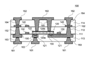
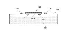
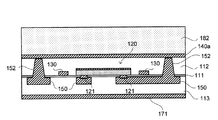
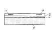
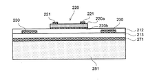
【解決手段】 主面120aにスタッドバンプ121が設けられた半導体IC120と、半導体IC120の主面120aを覆う第1の樹脂層111と、半導体IC120の裏面120bを覆う第2の樹脂層112とを備える。半導体IC120のスタッドバンプ121は、第1の樹脂層111の表面から突出している。スタッドバンプ121を第1の樹脂層111の表面から突出させる方法としては、ウエットブラスト法などを用いて第1の樹脂層111の厚さを全体的に減少させればよい。これにより、半導体IC120の電極ピッチが狭い場合であっても、正しくスタッドバンプ121の頭出しを行うことができる。
【選択図】 図1

Description

本発明は半導体IC内蔵基板及びその製造方法に関し、特に、電極ピッチが非常に狭い半導体ICを埋め込むのに好適な半導体IC内蔵基板及びその製造方法に関する。
近年、半導体IC搭載モジュールに対する小型化・薄型化の要求を満たすべく、搭載する半導体ICをベアチップの状態でプリント基板に搭載する提案が数多くなされている。ベアチップ状態の半導体ICは、パッケージングされた半導体ICに比べて電極ピッチが非常に狭いことから、これをプリント基板に搭載する場合、半導体ICに設けられた電極(以下、「パッド電極」という)とプリント基板に設けられた配線(以下、「配線パターン」という)との接続をどのようにして行うかが重要な問題となる。
パッド電極と配線パターンとを接続する一つの方法として、ワイヤボンディングによりこれらを接続する方法が知られている。この方法によれば、ベアチップ状態の半導体ICを比較的容易に実装可能であるものの、半導体ICを搭載する領域とボンディングワイヤを接続する領域とをプリント基板上の別平面とする必要があることから、実装面積が大きくなるという問題があった。
また、パッド電極と配線パターンとを接続する他の方法として、ベアチップ状態の半導体ICをプリント基板にフリップチップ接続する方法も知られている。この方法によれば、実装面積を小さくすることが可能であるものの、パッド電極と配線パターンとの機械的な接続強度を十分に確保するためには、パッド電極の表面に多層のアンダーバリアメタルを施す必要があるなど、工程が複雑になるという問題があった。
しかも、上述した2つの方法は、いずれもプリント基板の表面に半導体ICを搭載するものであることから、モジュール全体を薄くすることが困難であるという共通の問題があった。これを解決する方法としては、特許文献1〜7に記載されているように、プリント基板にキャビティを形成してその内部にベアチップ状態の半導体ICを埋め込み、これにより半導体IC内蔵基板を構成する方法が考えられる。
しかしながら、特許文献1〜7に記載された方法では、キャビティが形成された部分の強度を確保するためにプリント基板の厚さをある程度厚くする必要があり、これがモジュールの薄型化の妨げになるという問題があった。さらに、キャビティの平面方向の大きさを半導体ICの平面の方向の大きさよりもある程度大きく設定する必要があることから、パッド電極と配線パターンとの相対的な位置関係にずれが生じ、このため電極ピッチが100μm以下といった狭い半導体ICを用いることは非常に困難であった。
しかも、半導体ICを埋め込んだ度、レーザーを照射することによって個々のパッド電極を露出させていることから、半導体ICの電極ピッチが狭くなれば狭くなるほど、高い加工精度が要求されるばかりでなく、パッド電極の数に比例して加工時間が増大するという問題もあった。また、半導体ICの電極ピッチが狭くなると、レーザー照射によって形成するビアの径も小さくする必要があることから、ビア内部のデスミア処理が困難になるという問題もあった。
これに対し、特許文献8には、転写用基板に半導体ICを固定した状態で、プリント基板に設けられたポスト電極を転写用基板に設けられた位置決め穴に挿入することによって、未硬化又は半硬化状態である樹脂層に半導体ICを埋め込み、その後、研磨又はブラストによりパッド電極を露出させる方法が開示されている。この方法によれば、高精度に半導体ICを位置決めできるばかりでなく、レーザー照射によって個々のパッド電極を露出させる場合に生じる上記問題を解消することが可能となる。
しかしながら、特許文献8の方法は、プリント基板にあらかじめポスト電極を形成しておかなければならないという制約が生じるとともに、転写用基板の加工が必要であることから、必ずしも、全ての半導体IC内蔵基板の製造に適しているとは言えなかった。
その他、半導体IC内蔵基板の製造方法に関するものではないが、半導体ICに設けられた電極を頭出しする方法として、研磨又はブラストを用いた例が特許文献9〜11に開示されている。
特開平9−321408号公報 特開2002−246500号公報 特開2001−339165号公報 特開2002−50874号公報 特開2002−170840号公報 特開2002−246507号公報 特開2003−7896号公報 特開2005−64470号公報 特開平11−274241号公報 特開2001−250902号公報 特開2003−197655号公報
このように、従来の方法では、電極ピッチの狭い半導体ICを基板内に埋め込む場合、種々の問題が生じていた。本発明は、このような問題を解決すべくなされたものであって、電極ピッチが非常に狭い半導体ICを埋め込むのに好適な半導体IC内蔵基板及びその製造方法を提供することを目的とする。
本発明による半導体IC内蔵基板は、主面に導電性突起物が設けられた半導体ICと、前記半導体ICの前記主面を覆う第1の樹脂層と、前記半導体ICの前記裏面を覆う第2の樹脂層とを備え、前記半導体ICの前記導電性突起物は、前記第1の樹脂層の表面から突出していることを特徴とする。第1及び第2の樹脂層の少なくとも一方は、半導体ICの側面に接触していることが好ましい。また、第1の樹脂層は半導体ICの主面に接触しており、第2の樹脂層は半導体ICの裏面に接触していることもまた好ましい。
半導体ICの主面及び裏面のいずれか一方にダイアタッチフィルムを設け、半導体ICの主面及び裏面の前記一方がダイアタッチフィルムを介して第1及び第2の樹脂層のいずれか一方に覆われていても構わない。
本発明による半導体IC内蔵基板は、第1及び第2の樹脂層を貫通して設けられた貫通電極をさらに備えることが好ましい。また、半導体ICが薄型化されていることがより好ましい。
また、本発明による半導体IC内蔵基板は、第1の樹脂層の前記表面に形成され、導電性突起物に接続された配線パターンをさらに備え、配線パターンの導電性突起物上における幅が、導電性突起物の突出部分の径よりも小さいことが好ましい。
また、本発明による半導体IC内蔵基板の製造方法は、主面に導電性突起物が設けられた半導体ICを第1及び第2の樹脂層によって挟み込む第1の工程と、前記第1の樹脂層の厚さを減少させることにより、前記半導体ICの前記導電性突起物を前記第1の樹脂層の一方の表面から突出させる第2の工程と、前記第1の樹脂層の前記一方の表面に配線パターンを形成する第3の工程とを備えることを特徴とする。
第2の工程は、第1の樹脂層の一方の面をウエットブラスト処理することによって厚さを減少させることが好ましい。
また、第1の工程は、第1の樹脂層の他方の面と半導体ICの主面とが向き合うようこれらを重ねる工程と、第2の樹脂層の一方の面と半導体ICの裏面とが向き合うようこれらを重ねる工程とを含むことが好ましい。この場合、第1の工程においては、第1の樹脂層の一方又は他方の面に形成されたアライメントマークを基準として、半導体ICを第1の樹脂層の前記他方の面に搭載することが好ましい。
また、第1の工程は、第1の樹脂層の一方の面側に支持基板を貼り付けた状態で行うことが好ましい。この場合、第1の工程を行った後、第2の工程を行う前に、第2の樹脂層の他方の面側に他の支持基板を貼り付ける工程と、第1の樹脂層の一方の面側から支持基板を剥離する工程を行うことがより好ましい。
一方、第1の工程は、第2の樹脂層の一方の面と半導体ICの裏面とが向き合うようこれらを重ねる工程と、第1の樹脂層の他方の面と半導体ICの主面とが向き合うようこれらを重ねる工程とを含むこともまた好ましい。この場合、第1の工程においては、第2の樹脂層の一方又は他方の面に形成されたアライメントマークを基準として、半導体ICを第2の樹脂層の一方の面に搭載することが好ましい。また、第1の工程は、第2の樹脂層の他方の面側に支持基板を貼り付けた状態で行うことがより好ましい
第3の工程においては、配線パターンの導電性突起物上における幅を、導電性突起物の突出部分の径よりも小さく設定することが好ましい。また、第1及び第2の樹脂層を貫通する貫通電極を形成する第4の工程をさらに備えることもまた好ましい。
本発明によれば、半導体ICに設けられた導電性突起物を露出させる方法として、レーザー照射ではなく、ウエットブラスト法などによって第1の樹脂層の厚さを全体的に減少させていることから、電極ピッチが狭い場合であっても、正しく導電性突起物の頭出しを行うことができる。しかも、導電性突起物の数にかかわらず、短時間で頭出しを行うことが可能となる。また、レーザー照射によって微小なビアを形成する場合のように、スミアが発生しないことから、デスミア処理を省略することも可能となる。
また、半導体ICの搭載時に、アライメントマークを基準として位置合わせすれば、高い搭載位置精度を得ることができる。
さらに、第1の樹脂層上に形成する配線パターンの幅を、導電性突起物の突出部分の径よりも小さく設定すれば、電極ピッチが特に狭い場合であっても、ショート不良の発生を防止することが可能となる。
これらにより、本実施形態によれば、電極ピッチの狭い半導体ICを基板に埋め込む場合に従来生じていた種々の問題を解消することが可能となる。
以下、添付図面を参照しながら、本発明の好ましい実施の形態について詳細に説明する。
図1は本発明の好ましい第1の実施形態による半導体IC内蔵基板100の構造を示す略断面図である。
図1に示すように、本実施形態による半導体IC内蔵基板100は、積層された樹脂層111〜114と、樹脂層111と樹脂層112との間に埋め込まれた半導体IC120と、アライメントマーク130と、各種配線パターン140,150,161,162と、貫通電極152,163〜165とを備えて構成されている。半導体IC120のパッド電極(図1には示されていない)上には、導電性突起物の一種であるスタッドバンプ121がそれぞれ形成されており、各パッド電極は対応するスタッドバンプ121を介して、配線パターン150と電気的に接続されている。スタッドバンプ121は、図1に示すように、樹脂層111の表面から突出している。
但し、本発明において半導体IC120に設けられた導電性突起物がスタッドバンプに限定されるものではなく、プレートバンプ、メッキバンプ、ボールバンプなどの各種のバンプを用いることができる。導電性突起物としてスタッドバンプを用いる場合には、銀や銅をワイヤボンディングにて形成することができ、プレートバンプを用いる場合には、メッキ、スパッタ又は蒸着によって形成することができる。また、メッキバンプを用いる場合には、メッキによって形成することができ、ボールバンプを用いる場合には、半田ボールをランド電極上に載置した後、これを溶融させるか、クリーム半田をランド電極上に印刷した後、これを溶融させることによって形成することができる。導電性突起物に使用可能な金属種としては特に限定されず、例えば、金(Au)、銀(Ag)、銅(Cu)、ニッケル(Ni)、スズ(Sn)、クロム(Cr)、ニッケル・クロム合金(Ni−Cr)、半田などを使用することができる。また、導電性材料をスクリーン印刷し、これを硬化させた円錐状、円柱状等のバンプや、ナノペーストを印刷し、加熱によりこれを焼結させてなるバンプを用いることもできる。
スタッドバンプ121などの導電性突起物の高さは、5〜200μm程度に設定することが好ましく、10〜80μm程度に設定することが特に好ましい。これは、高さが5μm未満であると、後述するスタッドバンプ121の頭出し工程において、半導体IC120の主面120a上を覆っている樹脂層111が全て無くなり、半導体IC120の主面120aにダメージが加わるおそれがあるからである。一方、高さが200μmを超える導電性突起物の形成は困難であり、また、その高さのばらつきも大きくなってしまうからである。
尚、図1には示されていないが、最外層の配線パターン161,162の少なくとも一方には、コンデンサ等の受動部品を搭載することができる。
本実施形態による半導体IC内蔵基板100では、内蔵される半導体IC120は研磨により薄型化されており、これにより半導体IC内蔵基板100の全体の厚さを1mm以下、例えば、200μm程度まで薄くすることが可能である。また後述するように、本実施形態では、半導体IC120がアライメントマーク130に対して位置合わせがされており、このため、各スタッドバンプ121の平面方向における位置と各種配線パターン140,150,161,162との相対的な位置関係に生じるずれは非常に少ない。
図2は、半導体IC120の構造を示す略斜視図である。
図2に示すように、半導体IC120はベアチップ状態の半導体ICであり、その主面120aには多数のパッド電極121aが備えられている。後述するが、本実施形態による半導体IC内蔵基板100では、スタッドバンプ121の頭出しをウェットブラスト法により一括して行うため、従来のようにレーザー照射によってパッド電極を露出させる場合の問題が生じない。このため、特に限定されるものではないが、パッド電極121aのピッチ(電極ピッチ)が100μm以下、例えば60μmといった非常に狭い半導体ICを用いることが可能である。
また、半導体IC120の裏面120bは研磨されており、これにより半導体IC120の厚さt(主面120aから裏面120bまでの距離)は、通常の半導体ICに比べて非常に薄くされている。半導体IC120の厚さtについては、特に限定されないが、200μm以下、例えば20〜100μm程度に設定することが好ましい。裏面120bの研磨は、ウエハの状態で多数の半導体ICに対して一括して行い、その後、ダイシングにより個別の半導体IC120に分離することが好ましい。研磨により薄くする前にダイシングによって個別の半導体IC120に分離した場合には、熱硬化性樹脂等により半導体IC120の主面120aを覆った状態で裏面120bを研磨すれば作業効率が良い。
但し、本発明において、半導体IC120の薄型化方法が研磨に限定されるものではなく、他の方法、例えば、エッチング、プラズマ処理、レーザー照射、ブラスト処理による薄型化方法を用いても構わない。
また、各パッド電極121aには、スタッドバンプ121が形成されている。スタッドバンプ121の大きさについては、電極ピッチに応じて適宜設定すればよく、例えば、電極ピッチが約100μmである場合には、径を30〜80μm程度、高さを10〜80μm程度に設定すればよい。スタッドバンプ121の形成は、ダイシングにより個別の半導体IC120に分離した後、ワイヤボンダーを用いて各パッド電極121aにこれらを形成することにより行うことができる。スタッドバンプ121の材料としては、特に限定されるものではないが銅(Cu)を用いることが好ましい。スタッドバンプ121の材料として銅(Cu)を用いれば、金(Au)を用いた場合と比べ、パッド電極121aに対して高い接合強度を得ることが可能となり、信頼性が高められる。
図1に示すように、本実施形態による半導体IC内蔵基板100では、半導体IC120の主面120aが樹脂層111によって直接覆われ、半導体IC120の裏面120bが樹脂層112によって直接覆われている。また、半導体IC120のスタッドバンプ121は、樹脂層111の表面から突出しており、この突出部分において配線パターン150と接続されている。
また、半導体IC120の裏面120bには、金属層122が形成されている。金属層122は、半導体IC120の動作によって発生する熱の放熱経路としての役割を果たすとともに、半導体IC120の裏面120bに発生するクラックをより効果的に防止する役割を果たす。さらに、半導体IC120のハンドリング性を向上させる役割をも果たす。
金属層122は、樹脂層112,114を貫通して設けられた貫通電極165によって、最外層に形成された配線パターン162に接続されている。この貫通電極165は、半導体IC120が発する熱の放熱経路となることから、極めて効率よくマザーボードへと放熱することができる。このため、特に限定されるものではないが、半導体IC120の種類としては、CPUやDSPのように動作周波数が非常に高いデジタルICを選択することが可能である。
樹脂層111〜114の材料としては、リフロー耐久性を有する材料であれば熱硬化性、熱可塑性樹脂を問わず用いることができる。具体的には、エポキシ樹脂、ビスマレイミド−トリアジン樹脂(BTレジン)、フェノール樹脂、ビニルベンジル樹脂、ポリフェニレンエーテル(ポリフェニレンエーテルオキサイド)樹脂(PPE,PPO)、シアネート樹脂、ベンゾオキサジン樹脂、ポリイミド樹脂、芳香族ポリエステル樹脂、ポリフェニレンサルファイド樹脂、ポリエーテルイミド樹脂、ポリアリレート樹脂、ポリエーテルエーテルケトン樹脂などを選択することができる。また、ガラスクロス、アラミド、芳香族ポリエステル等の不織布に上記樹脂を含浸させた材料や上記樹脂にフィラーを含有させた材料を用いてもよい。
次に、図1に示す半導体IC内蔵基板100の製造方法について、図面を参照しながら説明する。
図3乃至図22は、図1に示す半導体IC内蔵基板100の製造方法を説明するための工程図である。
まず、図3に示すように、アライメントマーク130が形成された樹脂層111を用意し、これに支持基板181を貼り付ける。アライメントマーク130は、樹脂層111の表面に形成された導体層をパターニングすることをによって形成しても構わないし、樹脂層111の表面に転写法によって形成しても構わない。いずれにしても、アライメントマーク130は、半導体IC120の位置合わせに使用されることから、その形成位置については正確に制御する必要がある。尚、アライメントマーク130は、実際の配線パターンによって代用しても構わないし、アライメント専用のパターンであっても構わない。
支持基板181の材料については、特に限定されるものではないが、例えば、ニッケル(Ni)やステンレスを用いることができる。支持基板181の厚さについては、必要な機械的強度が確保される限り特に限定されず、例えば50〜2000μm程度に設定すればよい。一方、樹脂層111の厚さについては、少なくともスタッドバンプ121の高さを超える厚みを有している必要がある。
次に、図4に示すように、アライメントマーク130を用いて位置合わせしながら、半導体IC120を樹脂層111の表面に搭載する。本実施形態では、半導体IC120をフェイスダウン方式、つまり、主面120aを下側にして搭載する。このとき、樹脂層111は熱硬化性樹脂の場合は加熱により溶融させるか、熱可塑性樹脂の場合はその弾性によってスタッドバンプ121が樹脂層111にめり込む。これにより、半導体IC120は、樹脂層111に仮止めされた状態となる。また、半導体IC120の主面120aと樹脂層111は、接触した状態となる。樹脂層111の材料が熱硬化性樹脂である場合は、その後、加熱させることにより完全に固定することもできる。また熱可塑性樹脂である場合も、加熱・溶融により密着性を高めて固定することもできる。
次に、図5に示すように、未硬化又は半硬化状態である樹脂層112と導体層140aの積層シートを、樹脂層112と半導体IC120の裏面120bとが向き合うよう重ね、熱を加えながら両者をプレスする。これにより樹脂層112は硬化し、図6に示すように、半導体IC120の裏面120b及び側面120cが、樹脂層112によって完全に覆われた状態となる。また、樹脂層112の材料が熱可塑性材料である場合は、重ね合わせた後、やはり熱を加えながら両者をプレスすることにより、同様の状態となる。つまり、この時点で、半導体IC120は、樹脂層111,112に挟み込まれた状態となる。
次に、図6に示すように、半導体IC120からみて支持基板181とは反対側の表面に、別の支持基板182を貼り付ける。このようにして、別の支持基板182を貼り付けた後、図7に示すように、先に貼り付けた支持基板181を剥離する。
次に、図8に示すように、樹脂層111の表面をウエットブラスト法によりエッチングする。ウエットブラスト法は、エッチングする材料の展性によってエッチングレートが異なり、具体的には、相対的に展性の小さい材料(硬化した樹脂など)はエッチングレートが大きく、相対的に展性の大きい材料(金属など)はエッチングレートが小さくなる。このため、樹脂層111の表面をウエットブラスト法によりエッチングすると、エッチング量・エッチング条件の調整により、半導体IC120に設けられたスタッドバンプ121が樹脂層111の表面から突出した状態とすることができる。突出量については特に限定されるものではないが、0.1〜20μm程度に設定することが好ましい。
但し、樹脂層111の厚さを減少させる方法としては、ウエットブラスト法に限定されるものではなく、ドライブラスト法、イオンミリング法、プラズマエッチング法など、他のエッチング法を用いても構わない。但し、十分な選択比が確保できる点、高い加工精度が得られる点、並びに、作業効率に優れる点などから、ウエットブラスト法を用いることが非常に好ましい。尚、樹脂層111の厚さを減少させる方法として、バフなどを用いた研磨は、本発明においては不適格である。これは、バフなどを用いた研磨では、スタッドバンプ121と樹脂層111とが同一平面となり、スタッドバンプ121を突出させることができないばかりでなく、研磨条件によっては、スタッドバンプ121を構成する導電材料がバフの回転方向にスジとなって延在し、ショートの原因となるおそれがあるからである。
このように、スタッドバンプ121を露出させる方法として、従来のようにレーザー照射により樹脂層111にレーザビアを形成するのではなく、ウエットブラスト法などによって樹脂層111の厚さを全体的に減少させていることから、電極ピッチが狭い場合であっても、一括してスタッドバンプ121の頭出しを正しく行うことができる。
次に、図9に示すように、樹脂層111側からレーザーを照射することにより、樹脂層111,112を貫通する貫通孔112aを形成する。但し、貫通孔112aの形成は、レーザー照射以外の方法を用いても構わない。
次に、図10に示すように、スパッタリング法等の気相成長法により、貫通孔112aの内部を含む樹脂層111側の全表面に、薄い下地導体層151を形成する。これにより、導体層140aのうち貫通孔112aの底部にて露出する部分や、スタッドバンプ121の突出部分は、下地導体層151によって直接覆われることになる。但し、下地導体層151の形成においては、気相成長法の代わりに無電解メッキ法や蒸着法を用いても構わない。下地導体層151の不要部分はその後除去されることから、下地導体層151の厚さは十分に薄く設定する必要があり、0.005〜3μm程度、例えば0.3〜2μm程度に設定することが好ましい。
尚、本実施形態では、ウエットブラスト処理により、スタッドバンプ121が樹脂層111の表面から突出した状態となっていることから、下地導体層151を形成する前に、エッチング残渣の除去などの前処理を行う必要はない。つまり、スタッドバンプ121と樹脂層111とが同一平面であると、スタッドバンプ121の表面がエッチング残渣で覆われている可能性があり、そのまま下地導体層151を形成すると導通不良を起こす可能性がある。これに対し、本実施形態のように、樹脂層111の表面からスタッドバンプ121が突出するような条件でウエットブラスト処理すれば、スタッドバンプ121の表面からはエッチング残渣が確実に取り除かれるため、前処理などを行うことなく、下地導体層151を形成することが可能となる。
次に、図11に示すように、基材の両面、つまり、下地導体層151の表面及び支持基板182の表面に感光性のドライフィルム101,102をそれぞれ貼り付けた後、図示しないフォトマスクを用いてドライフィルム101を露光し、配線パターン150を形成すべき領域150aのドライフィルム101を除去する。これにより、配線パターン150を形成すべき領域150aにおいては、下地導体層151が露出した状態となる。
このときドライフィルム102の除去は行わず、これにより支持基板182の表面については実質的に全面が覆われた状態を保っておく。ドライフィルム101の厚さについては、配線パターン150よりもやや厚く設定する必要があり、例えば、配線パターン150の厚さを20μm程度とする場合には、ドライフィルム101の厚さとしては25μm程度に設定すればよい。一方、ドライフィルム102は、支持基板182の表面にメッキが施されるのを防止する目的で設けられるものであり、その厚さについては任意である。
ここで、配線パターン150を形成すべき領域150aには、図11に示すように、スタッドバンプ121に対応する領域が含まれている。電極ピッチが非常に狭い半導体IC120が用いられる場合、スタッドバンプ121と領域150aの平面方向における位置関係に大きなずれは許容されないが、本実施形態では、半導体IC120がアライメントマーク130に対して位置合わせされていることから、スタッドバンプ121と領域150aの平面方向における位置関係に生じるずれを少なくすることが可能となる。
ここで、図11に示す例では、配線パターン150を形成すべき領域150aの幅がスタッドバンプ121の径よりも大きく設定されているが、電極ピッチが特に狭い場合には、配線パターン150を形成すべき領域150aの幅をスタッドバンプ121の径よりも小さく設定することにより、製造マージンを確保することが可能である。
つまり、模式的な平面図である図12に示すように、スタッドバンプ121の突出部分の径をAとし、配線パターン150を形成すべき領域150aの幅をBとした場合、
A<B、又は
A=B
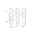
であると、図13に示すように、ドライフィルム101のパターニング時に大きなずれが生じた場合、一つの領域150a内に2つのスタッドバンプ121が含まれてしまうことになる。このようなずれが生じた場合、最終的にこれら2つのスタッドバンプ121は配線パターン150によって短絡されるため、ショート不良となってしまう。
このような問題は、スタッドバンプ121の突出部分の径をAとし、配線パターン150を形成すべき領域150aの幅をBとした場合、図14に示すように、
A>B
に設定することにより解決できる。これによれば、ドライフィルム101のパターニング時に多少のずれが生じたとしても、一つの領域150a内に2つのスタッドバンプ121が含まれてしまう可能性を低減することができる。具体的には、
A=B
である場合と比べ、
A−B
で与えられる距離だけマージンが拡大する。したがって、実現可能なマージンをXとすると、
B<A−X
を満たすように領域150aの幅Bを設定すれば、隣り合うスタッドバンプ121のショートを確実に防止することが可能となる。
但し、本発明において
A>B
に設定することは必須でなく、図12に示す例のように、
A<B、又は
A=B
であっても構わない。
このようにして下地導体層151の一部を露出させた後、図15に示すように、下地導体層151を基体とした電解メッキを行う。これにより、下地導体層151が露出している領域150aには、配線パターン150が形成される。したがって、領域150aの幅がBに設定されていれば、形成される配線パターン150の幅もBとなる。また、貫通孔112aの内部は貫通電極152によって満たされる。つまり、貫通電極152は、樹脂層111,112を貫通し、これにより、導体層140aと配線パターン150は貫通電極152を介して接続されることになる。支持基板182の表面については、実質的にその全面がドライフィルム102によって覆われていることから、メッキが形成されることはない。
メッキ液の種類については、配線パターン150及び貫通電極152を構成すべき材料に応じて適宜選択すればよく、例えば、これらの材料を銅(Cu)とする場合には、メッキ液として硫酸銅浴を用いればよい。
次に、図16に示すように、ドライフィルム101,102を剥離し、さらに、酸などのエッチング液を用いて配線パターン150が形成されていない部分の不要な下地導体層151を除去(ソフトエッチング)する。
次に、図17に示すように、樹脂層113と導体層171の積層シートをプレスし、加熱する。これにより図18に示すように、配線パターン150及び樹脂層111が樹脂層113によって覆われた状態となる。
次に、後に貼り付けた支持基板182を剥離し、露出した導体層140aをパターニングすることによって、図19に示すように配線パターン140を形成する。
次に、図20に示すように、樹脂層114と導体層172の積層シートをプレスし、加熱する。これにより、図21に示すように、配線パターン140及び樹脂層112が樹脂層114によって覆われた状態となる。
さらに、図22に示すように、導体層171,172を除去又は薄膜化した後、レーザー照射などによって貫通孔113a,114a,114bを形成する。貫通孔113aは、樹脂層113を貫通して配線パターン150を露出させる貫通孔であり、貫通孔114aは、樹脂層114を貫通して配線パターン140を露出させる貫通孔であり、貫通孔114bは、樹脂層114,112を貫通して金属層122を露出させる貫通孔である。
そして、貫通孔113a,114a,114bの内部を含む全表面に薄い下地導体層160を形成し、その後、図11、図15及び図16を用いて説明した工程と同様の工程を行うことにより、図1に示した最外面の配線パターン161,162を形成する。この工程により、貫通孔113aの内部は貫通電極163によって満たされ、これにより、配線パターン161と配線パターン150とが接続される。また、貫通孔114aの内部は貫通電極164によって満たされ、これにより、配線パターン162と配線パターン140とが接続される。さらに、貫通孔114bの内部は貫通電極165によって満たされ、これにより、配線パターン162と金属層122とが接続される。
このようにして、図1に示した半導体IC内蔵基板100が完成する。
以上説明したように、本実施形態においては、スタッドバンプ121を露出させる方法として、レーザー照射ではなく、ウエットブラスト法などによって樹脂層111の厚さを全体的に減少させていることから、電極ピッチが狭い場合であっても、正しくスタッドバンプ121の頭出しを行うことができる。しかも、スタッドバンプ121の数にかかわらず、短時間でスタッドバンプ121の頭出しを行うことが可能となる。また、レーザー照射によって微小なビアを形成する場合のように、スミアが発生しないことから、デスミア処理を省略することも可能となる。
特に、本実施形態では、スタッドバンプ121の頭出し方法としてウエットブラスト法を用い、エッチング量・エッチング条件の調整によって、スタッドバンプ121を樹脂層111の表面から突出させていることから、下地導体層151を形成する前に、エッチング残渣の除去などの前処理を行う必要もない。
さらに、半導体IC120の搭載時に、樹脂層111の表面に形成されたアライメントマーク130を基準として位置合わせしていることから、高い搭載位置精度を得ることができる。
これらにより、本実施形態によれば、電極ピッチの狭い半導体ICを基板に埋め込む場合に従来生じていた種々の問題を解消することが可能となる。しかも、本実施形態では、半導体IC120をフェイスダウン方式で搭載していることから、下側からスタッドバンプ121を画像認識しながら搭載することができるため、非常に高い搭載位置精度を得ることが可能となる。
また、本実施形態において用いている半導体IC120は、研磨などによりその厚さtが非常に薄く設定されていることから、半導体IC内蔵基板100全体の厚さを非常に薄く、例えば200μm程度とすることが可能となる。
さらに、本実施形態では、一連の工程の大部分において、仕掛かり中の基材を支持基板181又は支持基板182によって保持しながらプロセスを進めていることから、ハンドリング性が向上するとともに、基材のワレ、カケ、変形による半導体IC120への負荷を低減することができる。また、パターニング時における基材の寸法変化、歪みを防止することもできる。これらにより、スタッドバンプ121と配線パターン150とのずれや歪みを抑えることができ、接続安定性を高めることが可能となる。
しかも、配線パターン150の幅(B)がスタッドバンプ121の突出部分の径(A)よりも小さくなるように設定すれば、電極ピッチが特に狭い場合であっても、ショート不良の発生を防止することが可能となる。このような構成は、レーザー照射によってスタッドバンプ121を露出させる方法では採用困難であり、この点も、ウエットブラスト法によりスタッドバンプ121の頭出しを行う本実施形態の大きな利点である。
つまり、レーザー照射によってスタッドバンプ121を露出させる方法では、レーザー開口径の縮小は50μm〜80μm程度が限界である。しかも、レーザー照射時には不可避的に位置ずれが生じるため、スタッドバンプ121の径が例えば50〜60μm程度のサイズであると、レーザー照射により所望のスタッドバンプ121だけを正しく露出させるのは事実上不可能となる。また、レーザーでビアを形成した後、セミアディティブ法を用いて配線パターン150を形成する場合、配線パターン150の幅(B)をビアの径と同じかそれ以下に設定しようとすると、ドライフィルムの露光、現像、剥離性に問題が生じ、正しくパターニングできなくなってしまう。サブトラクティブ法を用いる場合も、ビアの径より配線パターン150の幅(B)を小さくすると、ビア内のメッキもエッチングされてしまい、オープン不良となってしまう。
このように、レーザー照射によってスタッドバンプ121を露出させる方法では、配線パターン150の幅(B)をスタッドバンプ121の径よりも小さく設定することは極めて困難である。これに対し、本実施形態では、ウエットブラスト法を用いてスタッドバンプ121の頭出しを行っていることから、このような問題が生じることがなく、配線パターン150の幅(B)をスタッドバンプ121の突出部分の径(A)よりも小さくなるように設定することが可能となる。
次に、本発明の好ましい第2の実施形態による半導体IC内蔵基板について説明する。
図23は本発明の好ましい第2の実施形態による半導体IC内蔵基板200の構造を示す略断面図である。
図23に示すように、本実施形態による半導体IC内蔵基板200は、積層された樹脂層211〜214と、樹脂層211と樹脂層212との間に埋め込まれた半導体IC220と、アライメントマーク230と、各種配線パターン250,261,262と、貫通電極252,263〜265とを備えて構成されている。半導体IC220は、図2に示した半導体IC120と同様の構成を有している。本実施形態においても、スタッドバンプ221は、樹脂層211の表面から突出しており、突出部分において配線パターン250と電気的に接続されている。
本実施形態においても、最外層の配線パターン261,262の少なくとも一方には、コンデンサ等の受動部品を搭載することができる。また、樹脂層211〜214の材料としては、上記第1の実施形態における樹脂層111〜114と同様の材料を用いることができる。
次に、図23に示す半導体IC内蔵基板200の製造方法について、図面を参照しながら説明する。
図24乃至図38は、図23に示す半導体IC内蔵基板200の製造方法を説明するための工程図である。
まず、図24に示すように、両面に導体層230a,271が形成された樹脂層213を用意し、これに支持基板281を貼り付ける。
次に、図25に示すように、導体層230aをパターニングし、これによりアライメントマーク230を形成する。本実施形態におけるアライメントマーク230は、実際の配線パターンとしても用いられるパターンである。
次に、図26に示すように、樹脂層213及びアライメントマーク230を覆う樹脂層212を形成する。
次に、図27に示すように、アライメントマーク230を用いて位置合わせしながら、半導体IC220を樹脂層212の表面に搭載する。本実施形態では、半導体IC220をフェイスアップ方式、つまり、主面220aを上側にして搭載する。これにより、半導体IC220の裏面220bは、樹脂層212によって完全に覆われた状態となる。
次に、図28に示すように、樹脂層211と導体層270の積層シートを、樹脂層211と半導体IC220の主面220aとが向き合うよう重ね、熱を加えながら両者をプレスする。これにより図29に示すように、半導体IC220の主面220a及び側面220cが、樹脂層211によって完全に覆われた状態となる。つまり、この時点で、半導体IC220は、樹脂層211,212に挟み込まれた状態となる。
次に、図30に示すように、導体層270を除去した後、樹脂層211の表面をウエットブラスト法等を用いてエッチングする。このとき、上記実施形態と同様、エッチング量・エッチング条件の調整によって、半導体IC220に設けられたスタッドバンプ221が樹脂層211の表面から突出させる。
次に、図31に示すように、樹脂層211側からレーザーを照射することにより、樹脂層211,212を貫通する貫通孔211aを形成する。但し、貫通孔211aの形成は、レーザー照射以外の方法を用いても構わない。
次に、図32に示すように、スパッタリング法等の気相成長法により、貫通孔211aの内部を含む樹脂層211側の全表面に、薄い下地導体層251を形成する。これにより、アライメントマーク230のうち貫通孔211aの底部にて露出する部分や、スタッドバンプ221の突出部分は、下地導体層251によって直接覆われることになる。本実施形態においても、ウエットブラスト処理により、スタッドバンプ221が樹脂層211の表面から突出した状態となっていることから、下地導体層251を形成する前に、エッチング残渣の除去などの前処理を行う必要はない。
次に、図33に示すように、基材の両面、つまり、下地導体層251の表面及び支持基板281の表面に感光性のドライフィルム201,202をそれぞれ貼り付けた後、図示しないフォトマスクを用いてドライフィルム201を露光し、配線パターン250を形成すべき領域250aのドライフィルム201を除去する。これにより、配線パターン250を形成すべき領域250aにおいては、下地導体層251が露出した状態となる。このときドライフィルム202の除去は行わず、これにより支持基板281の表面については実質的に全面が覆われた状態を保っておく。
本実施形態においても、配線パターン250を形成すべき領域250aには、図33に示すように、スタッドバンプ221に対応する領域が含まれているが、半導体IC220がアライメントマーク230に対して位置合わせされていることから、スタッドバンプ221と領域250aの平面方向における位置関係に生じるずれは少ない。
ここでも、電極ピッチが特に狭い場合には、スタッドバンプ221の突出部分の径をAとし、配線パターン250を形成すべき領域250aの幅をBとした場合、
A>B
に設定することが好ましい。
このようにして下地導体層251の一部を露出させた後、図34に示すように、下地導体層251を基体とした電解メッキを行う。これにより、下地導体層251が露出している領域250aには、配線パターン250が形成される。したがって、領域250aの幅がBに設定されていれば、形成される配線パターン250の幅もBとなる。また、貫通孔211aの内部は貫通電極252によって満たされる。つまり、貫通電極252は、樹脂層211,212を貫通し、これにより、アライメントマーク230と配線パターン250は貫通電極252を介して接続されることになる。支持基板281の表面については、実質的にその全面がドライフィルム202によって覆われていることから、メッキが形成されることはない。
次に、図35に示すように、ドライフィルム201,202を剥離し、さらに、酸などのエッチング液を用いて配線パターン250が形成されていない部分の不要な下地導体層251を除去(ソフトエッチング)する。
次に、図36に示すように、樹脂層214と導体層272の積層シートをプレスし、加熱する。これにより、図37に示すように、配線パターン250及び樹脂層211が樹脂層214によって覆われた状態となる。その後、支持基板281を剥離する。
さらに、図38に示すように、導体層271,272を除去又は薄膜化した後、レーザー照射などによって貫通孔213a,213b,214aを形成する。貫通孔213aは、樹脂層213を貫通してアライメントマーク230を露出させる貫通孔であり、貫通孔213bは、樹脂層213,212を貫通して金属層222を露出させる貫通孔であり、貫通孔214aは、樹脂層214を貫通して配線パターン250を露出させる貫通孔である。
そして、貫通孔213a,213b,214aの内部を含む全表面に薄い下地導体層260を形成し、その後、図33〜図35を用いて説明した工程と同様の工程を行うことにより、図23に示した最外面の配線パターン261,262を形成する。この工程により、貫通孔213aの内部は貫通電極263によって満たされ、これにより、配線パターン261とアライメントマーク230とが接続される。また、貫通孔213bの内部は貫通電極264によって満たされ、これにより、配線パターン261と金属層222とが接続される。さらに、貫通孔214aの内部は貫通電極265によって満たされ、これにより、配線パターン262と配線パターン250とが接続される。
このようにして、図23に示した半導体IC内蔵基板200が完成する。
以上説明したように、本実施形態においても、ウエットブラスト法などによって樹脂層211の厚さを全体的に減少させ、これにより、スタッドバンプ221を樹脂層211の表面から突出させていることから、上記実施形態と同様の効果を得ることが可能となる。しかも、本実施形態では、半導体IC220をフェイスアップ方式で搭載していることから、支持基板281が1枚で済み、工程の途中で張り替えを行う必要がなくなる。このため、より単純なプロセスによって基材の変形などを防止することが可能となる。
以上、本発明の好ましい実施形態について説明したが、本発明は、上記の実施形態に限定されることなく、本発明の主旨を逸脱しない範囲で種々の変更が可能であり、それらも本発明の範囲内に包含されるものであることはいうまでもない。
例えば、上述した第1及び第2の実施形態では、導体パターンをアライメントマークとして用いているが、アライメントマークが導体パターンに限定されるものではなく、樹脂層に設けた凹部などをアライメントマークとして利用しても構わない。一例として、図39に示すように、突起302を有する金型301を用いたプレスにより、樹脂層111に凹部130aを形成し、図40に示すように、この凹部130aをアライメントマークとして、半導体IC120を搭載しても構わない。
また、第1の実施形態では、アライメントマーク130を樹脂層111の表面のうち、半導体IC120が搭載される側の面に設けられているが、アライメントマーク130の位置としてはこれに限定されるものではなく、例えば、樹脂層111の反対側の表面に設けても構わない。同様に、第2の実施形態では、アライメントマーク230を樹脂層212の表面のうち、半導体IC220が搭載される側とは反対側の面に設けられているが、アライメントマーク230の位置としてはこれに限定されるものではなく、例えば、樹脂層212の反対側の表面に設けても構わない。
さらに、上述した第1及び第2の実施形態では、半導体ICを樹脂層に直接搭載しているが、半導体ICにダイアタッチフィルムを設け、ダイアタッチフィルムを介して樹脂層に搭載しても構わない。一例として、図41に示すように、半導体IC220の裏面にダイアタッチフィルム229を設け、ダイアタッチフィルム229と樹脂層212とを接着することによって、半導体IC220を樹脂層212に仮止めしても構わない。この場合、樹脂層212が接着性を有している必要はない。図42に示す例の場合、半導体IC200の裏面220bと樹脂層212との間にダイアタッチフィルム229が介在するため、両者は直接接触しなくなるが、半導体IC200の裏面220bは、ダイアタッチフィルム229を介して樹脂層212によって覆われることになる。
本発明の好ましい第1の実施形態による半導体IC内蔵基板100の構造を示す略断面図である。 半導体IC120の構造を示す略斜視図である。 半導体IC内蔵基板100の製造工程の一部(アライメントマーク130の形成)を示す図である。 半導体IC内蔵基板100の製造工程の一部(半導体IC120の搭載)を示す図である。 半導体IC内蔵基板100の製造工程の一部(樹脂層112のプレス)を示す図である。 半導体IC内蔵基板100の製造工程の一部(支持基板182の貼り付け)を示す図である。 半導体IC内蔵基板100の製造工程の一部(支持基板181の剥離)を示す図である。 半導体IC内蔵基板100の製造工程の一部(樹脂層111のエッチング)を示す図である。 半導体IC内蔵基板100の製造工程の一部(貫通孔112aの形成)を示す図である。 半導体IC内蔵基板100の製造工程の一部(下地導体層151の形成)を示す図である。 半導体IC内蔵基板100の製造工程の一部(ドライフィルム101,102の貼り付け及び露光)を示す図である。 スタッドバンプ121と配線パターン150を形成すべき領域150aとの関係を示す模式的な平面図であり、A<Bである場合を示している。 図12に示す領域150aに大きなずれが生じた状態を示す模式的な平面図である。 スタッドバンプ121と配線パターン150を形成すべき領域150aとの関係を示す模式的な平面図であり、A>Bである場合を示している。 半導体IC内蔵基板100の製造工程の一部(配線パターン150の形成)を示す図である。 半導体IC内蔵基板100の製造工程の一部(ドライフィルム101,102及び下地導体層151の除去)を示す図である。 半導体IC内蔵基板100の製造工程の一部(樹脂層113のプレス(プレス前))を示す図である。 半導体IC内蔵基板100の製造工程の一部(樹脂層113のプレス(プレス後))を示す図である。 半導体IC内蔵基板100の製造工程の一部(支持基板182の剥離)を示す図である。 半導体IC内蔵基板100の製造工程の一部(樹脂層114のプレス(プレス前))を示す図である。 半導体IC内蔵基板100の製造工程の一部(樹脂層114のプレス(プレス後))を示す図である。 半導体IC内蔵基板100の製造工程の一部(貫通孔113a,114a,114b及び下地導体層160の形成)を示す図である。 本発明の好ましい第2の実施形態による半導体IC内蔵基板200の構造を示す略断面図である。 半導体IC内蔵基板200の製造工程の一部(支持基板281の貼り付け)を示す図である。 半導体IC内蔵基板200の製造工程の一部(アライメントマーク230の形成)を示す図である。 半導体IC内蔵基板200の製造工程の一部(樹脂層212の形成)を示す図である。 半導体IC内蔵基板200の製造工程の一部(半導体IC220の搭載)を示す図である。 半導体IC内蔵基板200の製造工程の一部(樹脂層211のプレス(プレス前))を示す図である。 半導体IC内蔵基板200の製造工程の一部(樹脂層211のプレス(プレス後))を示す図である。 半導体IC内蔵基板200の製造工程の一部(樹脂層211のエッチング)を示す図である。 半導体IC内蔵基板200の製造工程の一部(貫通孔211aの形成)を示す図である。 半導体IC内蔵基板200の製造工程の一部(下地導体層251の形成)を示す図である。 半導体IC内蔵基板200の製造工程の一部(ドライフィルム201,202の貼り付け及び露光)を示す図である。 半導体IC内蔵基板200の製造工程の一部(配線パターン250の形成)を示す図である。 半導体IC内蔵基板200の製造工程の一部(ドライフィルム201,202及び下地導体層251の除去)を示す図である。 半導体IC内蔵基板200の製造工程の一部(樹脂層214のプレス(プレス前))を示す図である。 半導体IC内蔵基板200の製造工程の一部(樹脂層214のプレス(プレス後))を示す図である。 半導体IC内蔵基板200の製造工程の一部(貫通孔213a,213b,214a及び下地導体層260の形成)を示す図である。 樹脂層111に凹部130aを形成する方法を説明するための図である。 樹脂層111に設けた凹部130aをアライメントマークとして半導体IC120を搭載した状態を示す図である。 ダイアタッチフィルム229を介して半導体IC220を樹脂層212に搭載した状態を示す図である。
符号の説明
100,200 半導体IC内蔵基板
101,102,201,202 ドライフィルム
111〜114,211〜214 樹脂層
112a,113a,114a,114b,211a,213a,213b,214a 貫通孔
120,220 半導体IC
120a,220a 半導体ICの主面
120b,220b 半導体ICの裏面
120c,220c 半導体ICの側面
121,221 スタッドバンプ
121a パッド電極
122,222 金属層
130,230 アライメントマーク
130a 凹部
140,150,161,162,250,261,262 配線パターン
140a,171,172,230a,271,261,262,270,271,272 導体層
150a,250a 導体層を形成すべき領域
151,160,251,260 下地導体層
152,163〜165,252,263〜265 貫通電極
181,182,281 支持基板
229 ダイアタッチフィルム
301 金型
302 突起

Claims (18)

  1. 主面に導電性突起物が設けられた半導体ICと、前記半導体ICの前記主面を覆う第1の樹脂層と、前記半導体ICの裏面を覆う第2の樹脂層とを備え、前記半導体ICの前記導電性突起物は、前記第1の樹脂層の表面から突出していることを特徴とする半導体IC内蔵基板。
  2. 前記第1及び第2の樹脂層の少なくとも一方は、前記半導体ICの側面に接触していることを特徴とする請求項1に記載の半導体IC内蔵基板。
  3. 前記第1の樹脂層は前記半導体ICの前記主面に接触しており、前記第2の樹脂層は前記半導体ICの前記裏面に接触していることを特徴とする請求項1又は2に記載の半導体IC内蔵基板。
  4. 前記半導体ICの前記主面及び前記裏面のいずれか一方にはダイアタッチフィルムが設けられており、前記半導体ICの前記主面及び前記裏面の前記一方は、前記ダイアタッチフィルムを介して前記第1及び第2の樹脂層のいずれか一方に覆われていることを特徴とする請求項1又は2に記載の半導体IC内蔵基板。
  5. 前記第1及び第2の樹脂層を貫通して設けられた貫通電極をさらに備えることを特徴とする請求項1乃至4のいずれか一項に記載の半導体IC内蔵基板。
  6. 前記第1の樹脂層の前記表面に形成され、前記導電性突起物に接続された配線パターンをさらに備え、前記配線パターンの前記導電性突起物上における幅が、前記導電性突起物の突出部分の径よりも小さいことを特徴とする請求項1乃至5のいずれか一項に記載の半導体IC内蔵基板。
  7. 前記半導体ICが薄型化されていることを特徴とする請求項1乃至6のいずれか1項に記載の半導体IC内蔵基板。
  8. 主面に導電性突起物が設けられた半導体ICを第1及び第2の樹脂層によって挟み込む第1の工程と、
    前記第1の樹脂層の厚さを減少させることにより、前記半導体ICの前記導電性突起物を前記第1の樹脂層の一方の表面から突出させる第2の工程と、
    前記第1の樹脂層の前記一方の表面に配線パターンを形成する第3の工程とを備えることを特徴とする半導体IC内蔵基板の製造方法。
  9. 前記第2の工程は、前記第1の樹脂層の前記一方の面をウエットブラスト処理することによって厚さを減少させることを特徴とする請求項8に記載の半導体IC内蔵基板の製造方法。
  10. 前記第1の工程は、前記第1の樹脂層の他方の面と前記半導体ICの前記主面とが向き合うようこれらを重ねる工程と、前記第2の樹脂層の一方の面と前記半導体ICの裏面とが向き合うようこれらを重ねる工程とを含むことを特徴とする請求項8又は9に記載の半導体IC内蔵基板の製造方法。
  11. 前記第1の工程においては、前記第1の樹脂層の前記一方又は他方の面に形成されたアライメントマークを基準として、前記半導体ICを前記第1の樹脂層の前記他方の面に搭載することを特徴とする請求項10に記載の半導体IC内蔵基板の製造方法。
  12. 前記第1の工程は、前記第1の樹脂層の前記一方の面側に支持基板を貼り付けた状態で行うことを特徴とする請求項10又は11に記載の半導体IC内蔵基板の製造方法。
  13. 前記第1の工程を行った後、前記第2の工程を行う前に、前記第2の樹脂層の他方の面側に他の支持基板を貼り付ける工程と、前記第1の樹脂層の前記一方の面側から前記支持基板を剥離する工程を行うことを特徴とする請求項12に記載の半導体IC内蔵基板の製造方法。
  14. 前記第1の工程は、前記第2の樹脂層の一方の面と前記半導体ICの裏面とが向き合うようこれらを重ねる工程と、前記第1の樹脂層の他方の面と前記半導体ICの前記主面とが向き合うようこれらを重ねる工程とを含むことを特徴とする請求項8又は9に記載の半導体IC内蔵基板の製造方法。
  15. 前記第1の工程においては、前記第2の樹脂層前記一方又はの他方の面に形成されたアライメントマークを基準として、前記半導体ICを前記第2の樹脂層の前記一方の面に搭載することを特徴とする請求項14に記載の半導体IC内蔵基板の製造方法。
  16. 前記第1の工程は、前記第2の樹脂層の他方の面側に支持基板を貼り付けた状態で行うことを特徴とする請求項14又は15に記載の半導体IC内蔵基板の製造方法。
  17. 前記第3の工程においては、前記配線パターンの前記導電性突起物上における幅を、前記導電性突起物の突出部分の径よりも小さく設定することを特徴とする請求項8乃至16のいずれか一項に記載の半導体IC内蔵基板の製造方法。
  18. 前記第1及び第2の樹脂層を貫通する貫通電極を形成する第4の工程をさらに備えることを特徴とする請求項8乃至17のいずれか一項に記載の半導体IC内蔵基板の製造方法。
JP2006050475A 2005-09-28 2006-02-27 半導体ic内蔵基板及びその製造方法 Active JP4535002B2 (ja)

Priority Applications (7)

Application Number Priority Date Filing Date Title
JP2006050475A JP4535002B2 (ja) 2005-09-28 2006-02-27 半導体ic内蔵基板及びその製造方法
EP06254920.9A EP1770776B1 (en) 2005-09-28 2006-09-22 Method for manufacturing semiconductor ic-embedded substrate
TW095135324A TW200721419A (en) 2005-09-28 2006-09-25 Semiconductor IC-embedded substrate and method for manufacturing same
US11/527,829 US7544537B2 (en) 2005-09-28 2006-09-27 Semiconductor IC-embedded substrate and method for manufacturing same
CN2006101599557A CN1941339B (zh) 2005-09-28 2006-09-28 嵌入有半导体ic的基板及其制造方法
KR1020060094814A KR101176814B1 (ko) 2005-09-28 2006-09-28 반도체 ic 내장 기판 및 그 제조 방법
US12/435,385 US8026614B2 (en) 2005-09-28 2009-05-04 Semiconductor IC-embedded substrate and method for manufacturing same

Applications Claiming Priority (2)

Application Number Priority Date Filing Date Title
JP2005282231 2005-09-28
JP2006050475A JP4535002B2 (ja) 2005-09-28 2006-02-27 半導体ic内蔵基板及びその製造方法

Publications (2)

Publication Number Publication Date
JP2007123797A true JP2007123797A (ja) 2007-05-17
JP4535002B2 JP4535002B2 (ja) 2010-09-01

Family

ID=37478946

Family Applications (1)

Application Number Title Priority Date Filing Date
JP2006050475A Active JP4535002B2 (ja) 2005-09-28 2006-02-27 半導体ic内蔵基板及びその製造方法

Country Status (6)

Country Link
US (2) US7544537B2 (ja)
EP (1) EP1770776B1 (ja)
JP (1) JP4535002B2 (ja)
KR (1) KR101176814B1 (ja)
CN (1) CN1941339B (ja)
TW (1) TW200721419A (ja)

Cited By (11)

* Cited by examiner, † Cited by third party
Publication number Priority date Publication date Assignee Title
JP2008153536A (ja) * 2006-12-19 2008-07-03 Shinko Electric Ind Co Ltd 電子部品内蔵基板および電子部品内蔵基板の製造方法
WO2009101723A1 (ja) * 2008-02-11 2009-08-20 Ibiden Co., Ltd. 電子部品内蔵基板の製造方法
JP2010183084A (ja) * 2009-02-06 2010-08-19 Imbera Electronics Oy Emi保護を備えた電子モジュール
JP2011187912A (ja) * 2010-03-05 2011-09-22 Samsung Electro-Mechanics Co Ltd 電子素子内蔵型印刷回路基板及びその製造方法
WO2013065099A1 (ja) * 2011-10-31 2013-05-10 株式会社メイコー 部品内蔵基板の製造方法及びこの方法を用いて製造した部品内蔵基板
WO2013069093A1 (ja) * 2011-11-08 2013-05-16 株式会社メイコー 部品内蔵基板の製造方法及びこの方法を用いて製造した部品内蔵基板
JP2015536046A (ja) * 2012-09-29 2015-12-17 インテル・コーポレーション コアレス基板内に埋め込みrfダイを有するシステムインパッケージ
US10109571B2 (en) 2015-10-07 2018-10-23 Fujitsu Limited Wiring substrate and manufacturing method of wiring substrate
WO2019186780A1 (ja) * 2018-03-28 2019-10-03 株式会社Fuji 回路形成方法、および回路形成装置
WO2022224438A1 (ja) * 2021-04-23 2022-10-27 日本電子材料株式会社 プローブカード及びプローブカード補修方法
WO2023286429A1 (ja) * 2021-07-12 2023-01-19 東洋紡株式会社 回路基板の製造方法、離型フィルム付き回路基板前駆体、及び、無機基板付き回路基板前駆体

Families Citing this family (45)

* Cited by examiner, † Cited by third party
Publication number Priority date Publication date Assignee Title
US7547975B2 (en) * 2003-07-30 2009-06-16 Tdk Corporation Module with embedded semiconductor IC and method of fabricating the module
US7569422B2 (en) 2006-08-11 2009-08-04 Megica Corporation Chip package and method for fabricating the same
JPWO2008120755A1 (ja) * 2007-03-30 2010-07-15 日本電気株式会社 機能素子内蔵回路基板及びその製造方法、並びに電子機器
US8106496B2 (en) * 2007-06-04 2012-01-31 Stats Chippac, Inc. Semiconductor packaging system with stacking and method of manufacturing thereof
JP5496445B2 (ja) * 2007-06-08 2014-05-21 ルネサスエレクトロニクス株式会社 半導体装置の製造方法
US20090014852A1 (en) * 2007-07-11 2009-01-15 Hsin-Hui Lee Flip-Chip Packaging with Stud Bumps
JPWO2009118925A1 (ja) 2008-03-27 2011-07-21 イビデン株式会社 電子部品内蔵配線板及びその製造方法
KR101486423B1 (ko) * 2008-07-04 2015-01-27 삼성전자주식회사 반도체 패키지
KR101033939B1 (ko) * 2009-06-01 2011-05-11 주식회사 심텍 임베디드 boc형 인쇄회로기판 및 그 제조방법
KR20110037332A (ko) * 2009-10-06 2011-04-13 삼성전기주식회사 인쇄회로기판 및 그 제조방법
JP5685811B2 (ja) * 2009-12-25 2015-03-18 富士通セミコンダクター株式会社 半導体装置及びその製造方法
US8426251B2 (en) * 2010-01-07 2013-04-23 Infineon Technologies Ag Semiconductor device
US8183696B2 (en) * 2010-03-31 2012-05-22 Infineon Technologies Ag Packaged semiconductor device with encapsulant embedding semiconductor chip that includes contact pads
US8558392B2 (en) * 2010-05-14 2013-10-15 Stats Chippac, Ltd. Semiconductor device and method of forming interconnect structure and mounting semiconductor die in recessed encapsulant
US8238113B2 (en) * 2010-07-23 2012-08-07 Imbera Electronics Oy Electronic module with vertical connector between conductor patterns
KR101150036B1 (ko) * 2010-08-11 2012-05-30 삼성테크윈 주식회사 전자소자 내장형 다층 연성인쇄회로기판 및 그 제조 방법
EP2624286B1 (en) * 2010-09-30 2020-11-11 Fuji Electric Co., Ltd. Method of manufacturing a semiconductor device
EP2448378A1 (en) * 2010-10-26 2012-05-02 ATOTECH Deutschland GmbH Composite build-up materials for embedding of active components
EP2506330A1 (en) 2011-04-01 2012-10-03 Nederlandse Organisatie voor toegepast -natuurwetenschappelijk onderzoek TNO Apparatus and method for providing an embedded structure and for providing an electro-optical device including the same
JP5640892B2 (ja) * 2011-05-23 2014-12-17 三菱電機株式会社 半導体装置
US8884432B2 (en) 2011-06-08 2014-11-11 Tessera, Inc. Substrate and assembly thereof with dielectric removal for increased post height
KR101905893B1 (ko) * 2012-06-13 2018-10-08 에스케이하이닉스 주식회사 복수의 유전층을 포함하는 임베디드 패키지 및 제조 방법
US8872349B2 (en) 2012-09-11 2014-10-28 Intel Corporation Bridge interconnect with air gap in package assembly
JP6033872B2 (ja) 2012-09-11 2016-11-30 株式会社メイコー 部品内蔵基板の製造方法
US9265147B2 (en) * 2012-11-14 2016-02-16 Fujikura Ltd. Multi-layer wiring board
US9788466B2 (en) 2013-04-16 2017-10-10 Skyworks Solutions, Inc. Apparatus and methods related to ground paths implemented with surface mount devices
US9793218B2 (en) 2013-05-14 2017-10-17 Meiko Electronics Co., Ltd. Method for manufacturing device embedded substrate, and device embedded substrate
US9147663B2 (en) * 2013-05-28 2015-09-29 Intel Corporation Bridge interconnection with layered interconnect structures
US8912663B1 (en) 2013-06-28 2014-12-16 Delta Electronics, Inc. Embedded package structure and method for manufacturing thereof
US9543373B2 (en) 2013-10-23 2017-01-10 Taiwan Semiconductor Manufacturing Company, Ltd. Semiconductor structure and manufacturing method thereof
SG10201400390YA (en) 2014-03-05 2015-10-29 Delta Electronics Int L Singapore Pte Ltd Package structure
SG10201400396WA (en) 2014-03-05 2015-10-29 Delta Electronics Int’L Singapore Pte Ltd Package structure and stacked package module with the same
KR20150137001A (ko) * 2014-05-28 2015-12-08 쿄세라 서킷 솔루션즈 가부시키가이샤 배선 기판의 제조방법
TWI549235B (zh) * 2014-07-03 2016-09-11 矽品精密工業股份有限公司 封裝結構及其製法與定位構形
US9837484B2 (en) * 2015-05-27 2017-12-05 STATS ChipPAC Pte. Ltd. Semiconductor device and method of forming substrate including embedded component with symmetrical structure
US9859234B2 (en) 2015-08-06 2018-01-02 Invensas Corporation Methods and structures to repair device warpage
CN110024111B (zh) * 2016-12-30 2024-03-19 英特尔公司 带有具有用于扇出缩放的柱和过孔连接的高密度互连层的封装衬底
CN106783765A (zh) * 2017-01-23 2017-05-31 合肥雷诚微电子有限责任公司 一种小型化高散热性的线性功率放大器结构及其制作方法
DE102018107035B4 (de) * 2017-11-15 2021-07-01 Taiwan Semiconductor Manufacturing Co., Ltd. Halbleiter-Package und Verfahren
US11031342B2 (en) 2017-11-15 2021-06-08 Taiwan Semiconductor Manufacturing Company, Ltd. Semiconductor package and method
US10461005B2 (en) 2018-04-02 2019-10-29 Advanced Semiconductor Engineering, Inc. Semiconductor package
US11277917B2 (en) 2019-03-12 2022-03-15 Advanced Semiconductor Engineering, Inc. Embedded component package structure, embedded type panel substrate and manufacturing method thereof
US11296030B2 (en) 2019-04-29 2022-04-05 Advanced Semiconductor Engineering, Inc. Embedded component package structure and manufacturing method thereof
US10950551B2 (en) 2019-04-29 2021-03-16 Advanced Semiconductor Engineering, Inc. Embedded component package structure and manufacturing method thereof
KR20220013703A (ko) * 2020-07-27 2022-02-04 삼성전기주식회사 전자부품 내장기판

Citations (6)

* Cited by examiner, † Cited by third party
Publication number Priority date Publication date Assignee Title
JP2001267366A (ja) * 2000-03-16 2001-09-28 Matsushita Electric Ind Co Ltd 半導体実装方法およびプリント回路基板
JP2005064470A (ja) * 2003-07-30 2005-03-10 Tdk Corp 半導体ic内蔵モジュール及びその製造方法
JP2005159226A (ja) * 2003-11-28 2005-06-16 Matsushita Electric Ind Co Ltd 回路部品内蔵基板およびその製造方法
JP2005217372A (ja) * 2004-02-02 2005-08-11 Sony Corp 電子部品を内蔵する基板、基板およびそれらの製造方法
JP2005229065A (ja) * 2004-02-16 2005-08-25 Fujikura Ltd 多層及び両面基板の製造方法
JP2005236039A (ja) * 2004-02-19 2005-09-02 Tdk Corp 半導体ic内蔵基板及びその製造方法、並びに、半導体ic内蔵モジュール

Family Cites Families (41)

* Cited by examiner, † Cited by third party
Publication number Priority date Publication date Assignee Title
US4926239A (en) 1983-06-07 1990-05-15 Sharp Kabushiki Kaisha Plastic encapsulant for semiconductor
JP2529987B2 (ja) 1988-01-18 1996-09-04 株式会社東芝 多層印刷配線板装置の製造方法
US4980753A (en) 1988-11-21 1990-12-25 Honeywell Inc. Low-cost high-performance semiconductor chip package
US4941255A (en) 1989-11-15 1990-07-17 Eastman Kodak Company Method for precision multichip assembly
US5745984A (en) 1995-07-10 1998-05-05 Martin Marietta Corporation Method for making an electronic module
JP2842378B2 (ja) 1996-05-31 1999-01-06 日本電気株式会社 電子回路基板の高密度実装構造
JP3751587B2 (ja) 1996-07-12 2006-03-01 富士通株式会社 半導体装置の製造方法
JP3662260B2 (ja) 1996-09-24 2005-06-22 三菱電機株式会社 半導体装置およびその製造方法
US5994166A (en) 1997-03-10 1999-11-30 Micron Technology, Inc. Method of constructing stacked packages
JP3349058B2 (ja) 1997-03-21 2002-11-20 ローム株式会社 複数のicチップを備えた半導体装置の構造
US6104093A (en) 1997-04-24 2000-08-15 International Business Machines Corporation Thermally enhanced and mechanically balanced flip chip package and method of forming
US6525414B2 (en) 1997-09-16 2003-02-25 Matsushita Electric Industrial Co., Ltd. Semiconductor device including a wiring board and semiconductor elements mounted thereon
JP3326382B2 (ja) 1998-03-26 2002-09-24 松下電器産業株式会社 半導体装置の製造方法
US6338980B1 (en) * 1999-08-13 2002-01-15 Citizen Watch Co., Ltd. Method for manufacturing chip-scale package and manufacturing IC chip
JP3813402B2 (ja) * 2000-01-31 2006-08-23 新光電気工業株式会社 半導体装置の製造方法
JP4854845B2 (ja) 2000-02-25 2012-01-18 イビデン株式会社 多層プリント配線板
JP4854847B2 (ja) 2000-02-25 2012-01-18 イビデン株式会社 多層プリント配線板および多層プリント配線板の製造方法
DE10010820C1 (de) * 2000-02-29 2001-09-13 Infineon Technologies Ag Verfahren zur Regenerierung von Halbleiterscheiben
JP2001250902A (ja) 2000-03-08 2001-09-14 Toshiba Corp 半導体パッケージ及びその製造方法
JP3597754B2 (ja) 2000-04-24 2004-12-08 Necエレクトロニクス株式会社 半導体装置及びその製造方法
US6753483B2 (en) 2000-06-14 2004-06-22 Matsushita Electric Industrial Co., Ltd. Printed circuit board and method of manufacturing the same
JP4931283B2 (ja) 2000-09-25 2012-05-16 イビデン株式会社 プリント配線板及びプリント配線板の製造方法
JP4601158B2 (ja) 2000-12-12 2010-12-22 イビデン株式会社 多層プリント配線板およびその製造方法
JP3420748B2 (ja) 2000-12-14 2003-06-30 松下電器産業株式会社 半導体装置及びその製造方法
JP4934900B2 (ja) 2000-12-15 2012-05-23 イビデン株式会社 多層プリント配線板の製造方法
TW511415B (en) * 2001-01-19 2002-11-21 Matsushita Electric Ind Co Ltd Component built-in module and its manufacturing method
JP3553043B2 (ja) 2001-01-19 2004-08-11 松下電器産業株式会社 部品内蔵モジュールとその製造方法
US6429045B1 (en) 2001-02-07 2002-08-06 International Business Machines Corporation Structure and process for multi-chip chip attach with reduced risk of electrostatic discharge damage
JP4243922B2 (ja) 2001-06-26 2009-03-25 イビデン株式会社 多層プリント配線板
US6794751B2 (en) * 2001-06-29 2004-09-21 Intel Corporation Multi-purpose planarizing/back-grind/pre-underfill arrangements for bumped wafers and dies
JP4856328B2 (ja) * 2001-07-13 2012-01-18 ローム株式会社 半導体装置の製造方法
JP2003037205A (ja) 2001-07-23 2003-02-07 Sony Corp Icチップ内蔵多層基板及びその製造方法
US6555924B2 (en) 2001-08-18 2003-04-29 Siliconware Precision Industries Co., Ltd. Semiconductor package with flash preventing mechanism and fabrication method thereof
TW200302685A (en) 2002-01-23 2003-08-01 Matsushita Electric Ind Co Ltd Circuit component built-in module and method of manufacturing the same
JP3865639B2 (ja) 2002-01-28 2007-01-10 信越化学工業株式会社 半導体封止用シリコーン組成物および半導体装置
JP3941573B2 (ja) * 2002-04-24 2007-07-04 宇部興産株式会社 フレキシブル両面基板の製造方法
US7122404B2 (en) * 2003-03-11 2006-10-17 Micron Technology, Inc. Techniques for packaging a multiple device component
US7547975B2 (en) 2003-07-30 2009-06-16 Tdk Corporation Module with embedded semiconductor IC and method of fabricating the module
TWI320583B (en) * 2003-12-26 2010-02-11 Advanced Semiconductor Eng Process for backside grinding a bumped wafer
JP4575071B2 (ja) * 2004-08-02 2010-11-04 新光電気工業株式会社 電子部品内蔵基板の製造方法
US7388297B2 (en) * 2005-08-26 2008-06-17 Oki Electric Industry Co., Ltd. Semiconductor device with reduced thickness of the semiconductor substrate

Patent Citations (6)

* Cited by examiner, † Cited by third party
Publication number Priority date Publication date Assignee Title
JP2001267366A (ja) * 2000-03-16 2001-09-28 Matsushita Electric Ind Co Ltd 半導体実装方法およびプリント回路基板
JP2005064470A (ja) * 2003-07-30 2005-03-10 Tdk Corp 半導体ic内蔵モジュール及びその製造方法
JP2005159226A (ja) * 2003-11-28 2005-06-16 Matsushita Electric Ind Co Ltd 回路部品内蔵基板およびその製造方法
JP2005217372A (ja) * 2004-02-02 2005-08-11 Sony Corp 電子部品を内蔵する基板、基板およびそれらの製造方法
JP2005229065A (ja) * 2004-02-16 2005-08-25 Fujikura Ltd 多層及び両面基板の製造方法
JP2005236039A (ja) * 2004-02-19 2005-09-02 Tdk Corp 半導体ic内蔵基板及びその製造方法、並びに、半導体ic内蔵モジュール

Cited By (18)

* Cited by examiner, † Cited by third party
Publication number Priority date Publication date Assignee Title
JP2008153536A (ja) * 2006-12-19 2008-07-03 Shinko Electric Ind Co Ltd 電子部品内蔵基板および電子部品内蔵基板の製造方法
WO2009101723A1 (ja) * 2008-02-11 2009-08-20 Ibiden Co., Ltd. 電子部品内蔵基板の製造方法
US8225503B2 (en) 2008-02-11 2012-07-24 Ibiden Co., Ltd. Method for manufacturing board with built-in electronic elements
JP2010183084A (ja) * 2009-02-06 2010-08-19 Imbera Electronics Oy Emi保護を備えた電子モジュール
US10470346B2 (en) 2009-02-06 2019-11-05 Ge Embedded Electronics Oy Electronic module with EMI protection
KR101781446B1 (ko) * 2009-02-06 2017-09-25 임베라 일렉트로닉스 오와이 Emi 보호 기능을 갖는 전자 모듈
JP2011187912A (ja) * 2010-03-05 2011-09-22 Samsung Electro-Mechanics Co Ltd 電子素子内蔵型印刷回路基板及びその製造方法
JPWO2013065099A1 (ja) * 2011-10-31 2015-04-02 株式会社メイコー 部品内蔵基板の製造方法及びこの方法を用いて製造した部品内蔵基板
US9526182B2 (en) 2011-10-31 2016-12-20 Meiko Electronics Co., Ltd. Component-embedded substrate manufacturing method
WO2013065099A1 (ja) * 2011-10-31 2013-05-10 株式会社メイコー 部品内蔵基板の製造方法及びこの方法を用いて製造した部品内蔵基板
JPWO2013069093A1 (ja) * 2011-11-08 2015-04-02 株式会社メイコー 部品内蔵基板の製造方法及びこの方法を用いて製造した部品内蔵基板
WO2013069093A1 (ja) * 2011-11-08 2013-05-16 株式会社メイコー 部品内蔵基板の製造方法及びこの方法を用いて製造した部品内蔵基板
JP2015536046A (ja) * 2012-09-29 2015-12-17 インテル・コーポレーション コアレス基板内に埋め込みrfダイを有するシステムインパッケージ
US10109571B2 (en) 2015-10-07 2018-10-23 Fujitsu Limited Wiring substrate and manufacturing method of wiring substrate
WO2019186780A1 (ja) * 2018-03-28 2019-10-03 株式会社Fuji 回路形成方法、および回路形成装置
JPWO2019186780A1 (ja) * 2018-03-28 2020-12-03 株式会社Fuji 回路形成方法、および回路形成装置
WO2022224438A1 (ja) * 2021-04-23 2022-10-27 日本電子材料株式会社 プローブカード及びプローブカード補修方法
WO2023286429A1 (ja) * 2021-07-12 2023-01-19 東洋紡株式会社 回路基板の製造方法、離型フィルム付き回路基板前駆体、及び、無機基板付き回路基板前駆体

Also Published As

Publication number Publication date
JP4535002B2 (ja) 2010-09-01
US7544537B2 (en) 2009-06-09
KR20070036007A (ko) 2007-04-02
KR101176814B1 (ko) 2012-08-24
CN1941339B (zh) 2011-09-14
EP1770776B1 (en) 2015-08-12
US20070069363A1 (en) 2007-03-29
US20090218678A1 (en) 2009-09-03
CN1941339A (zh) 2007-04-04
TW200721419A (en) 2007-06-01
US8026614B2 (en) 2011-09-27
EP1770776A2 (en) 2007-04-04
EP1770776A3 (en) 2007-12-05

Similar Documents

Publication Publication Date Title
JP4535002B2 (ja) 半導体ic内蔵基板及びその製造方法
JP4835124B2 (ja) 半導体ic内蔵基板及びその製造方法
TWI451536B (zh) 多層配線基板及其製造方法
JP4897281B2 (ja) 配線基板の製造方法及び電子部品実装構造体の製造方法
JP5164362B2 (ja) 半導体内臓基板およびその製造方法
JP3938921B2 (ja) 半導体ic内蔵モジュールの製造方法
US20120119391A1 (en) Semiconductor package and manufacturing method thereof
JP2011096903A (ja) 半導体素子実装配線基板の製造方法
US20060273451A1 (en) Semiconductor IC and its manufacturing method, and module with embedded semiconductor IC and its manufacturing method
JP5734624B2 (ja) 半導体パッケージの製造方法
JP2004119729A (ja) 回路装置の製造方法
KR100994099B1 (ko) 플립칩 기판 제조 방법
US7045393B2 (en) Method for manufacturing circuit devices
JP2005353837A (ja) 半導体装置及びその製造方法
KR20190068421A (ko) 배선 기판 및 그 제조 방법
JP2010283300A (ja) 突起電極付き配線基板及び突起電極付き配線基板の製造方法
JP2010123632A (ja) 電子部品内蔵配線基板の製造方法
JP2014220402A (ja) 半導体パッケージ基板の製造方法
JP7052464B2 (ja) 微細配線層付きコアレス基板の製造方法、および半導体パッケージの製造方法
JP2007012761A (ja) 半導体ic内蔵基板及びその製造方法
JP5098313B2 (ja) 配線基板
JP2007012762A (ja) 半導体ic内蔵基板及びその製造方法
JP2000277898A (ja) ボールグリッドアレイパッケージ実装用基板
JP3632719B2 (ja) リードフレーム及びリードフレームの製造方法
JP4398550B2 (ja) バンプ付き多層基板の製造方法

Legal Events

Date Code Title Description
A521 Request for written amendment filed

Free format text: JAPANESE INTERMEDIATE CODE: A523

Effective date: 20070309

A621 Written request for application examination

Free format text: JAPANESE INTERMEDIATE CODE: A621

Effective date: 20070309

A977 Report on retrieval

Free format text: JAPANESE INTERMEDIATE CODE: A971007

Effective date: 20090527

A131 Notification of reasons for refusal

Free format text: JAPANESE INTERMEDIATE CODE: A131

Effective date: 20090602

A521 Request for written amendment filed

Free format text: JAPANESE INTERMEDIATE CODE: A523

Effective date: 20090730

A02 Decision of refusal

Free format text: JAPANESE INTERMEDIATE CODE: A02

Effective date: 20100119

A521 Request for written amendment filed

Free format text: JAPANESE INTERMEDIATE CODE: A523

Effective date: 20100224

A911 Transfer to examiner for re-examination before appeal (zenchi)

Free format text: JAPANESE INTERMEDIATE CODE: A911

Effective date: 20100426

TRDD Decision of grant or rejection written
A01 Written decision to grant a patent or to grant a registration (utility model)

Free format text: JAPANESE INTERMEDIATE CODE: A01

Effective date: 20100525

A01 Written decision to grant a patent or to grant a registration (utility model)

Free format text: JAPANESE INTERMEDIATE CODE: A01

A61 First payment of annual fees (during grant procedure)

Free format text: JAPANESE INTERMEDIATE CODE: A61

Effective date: 20100607

FPAY Renewal fee payment (event date is renewal date of database)

Free format text: PAYMENT UNTIL: 20130625

Year of fee payment: 3

R150 Certificate of patent or registration of utility model

Ref document number: 4535002

Country of ref document: JP

Free format text: JAPANESE INTERMEDIATE CODE: R150

Free format text: JAPANESE INTERMEDIATE CODE: R150

FPAY Renewal fee payment (event date is renewal date of database)

Free format text: PAYMENT UNTIL: 20140625

Year of fee payment: 4