JP2006111969A - スパッタターゲットの製造方法 - Google Patents
スパッタターゲットの製造方法 Download PDFInfo
- Publication number
- JP2006111969A JP2006111969A JP2005276818A JP2005276818A JP2006111969A JP 2006111969 A JP2006111969 A JP 2006111969A JP 2005276818 A JP2005276818 A JP 2005276818A JP 2005276818 A JP2005276818 A JP 2005276818A JP 2006111969 A JP2006111969 A JP 2006111969A
- Authority
- JP
- Japan
- Prior art keywords
- wiring
- film
- sputter target
- manufacturing
- ingot
- Prior art date
- Legal status (The legal status is an assumption and is not a legal conclusion. Google has not performed a legal analysis and makes no representation as to the accuracy of the status listed.)
- Granted
Links
Images


Classifications
-
- H—ELECTRICITY
- H01—ELECTRIC ELEMENTS
- H01L—SEMICONDUCTOR DEVICES NOT COVERED BY CLASS H10
- H01L21/00—Processes or apparatus adapted for the manufacture or treatment of semiconductor or solid state devices or of parts thereof
- H01L21/02—Manufacture or treatment of semiconductor devices or of parts thereof
- H01L21/04—Manufacture or treatment of semiconductor devices or of parts thereof the devices having at least one potential-jump barrier or surface barrier, e.g. PN junction, depletion layer or carrier concentration layer
- H01L21/18—Manufacture or treatment of semiconductor devices or of parts thereof the devices having at least one potential-jump barrier or surface barrier, e.g. PN junction, depletion layer or carrier concentration layer the devices having semiconductor bodies comprising elements of Group IV of the Periodic System or AIIIBV compounds with or without impurities, e.g. doping materials
- H01L21/30—Treatment of semiconductor bodies using processes or apparatus not provided for in groups H01L21/20 - H01L21/26
- H01L21/31—Treatment of semiconductor bodies using processes or apparatus not provided for in groups H01L21/20 - H01L21/26 to form insulating layers thereon, e.g. for masking or by using photolithographic techniques; After treatment of these layers; Selection of materials for these layers
- H01L21/3205—Deposition of non-insulating-, e.g. conductive- or resistive-, layers on insulating layers; After-treatment of these layers
- H01L21/32051—Deposition of metallic or metal-silicide layers
-
- C—CHEMISTRY; METALLURGY
- C23—COATING METALLIC MATERIAL; COATING MATERIAL WITH METALLIC MATERIAL; CHEMICAL SURFACE TREATMENT; DIFFUSION TREATMENT OF METALLIC MATERIAL; COATING BY VACUUM EVAPORATION, BY SPUTTERING, BY ION IMPLANTATION OR BY CHEMICAL VAPOUR DEPOSITION, IN GENERAL; INHIBITING CORROSION OF METALLIC MATERIAL OR INCRUSTATION IN GENERAL
- C23C—COATING METALLIC MATERIAL; COATING MATERIAL WITH METALLIC MATERIAL; SURFACE TREATMENT OF METALLIC MATERIAL BY DIFFUSION INTO THE SURFACE, BY CHEMICAL CONVERSION OR SUBSTITUTION; COATING BY VACUUM EVAPORATION, BY SPUTTERING, BY ION IMPLANTATION OR BY CHEMICAL VAPOUR DEPOSITION, IN GENERAL
- C23C14/00—Coating by vacuum evaporation, by sputtering or by ion implantation of the coating forming material
- C23C14/06—Coating by vacuum evaporation, by sputtering or by ion implantation of the coating forming material characterised by the coating material
- C23C14/14—Metallic material, boron or silicon
-
- C—CHEMISTRY; METALLURGY
- C22—METALLURGY; FERROUS OR NON-FERROUS ALLOYS; TREATMENT OF ALLOYS OR NON-FERROUS METALS
- C22C—ALLOYS
- C22C21/00—Alloys based on aluminium
-
- C—CHEMISTRY; METALLURGY
- C23—COATING METALLIC MATERIAL; COATING MATERIAL WITH METALLIC MATERIAL; CHEMICAL SURFACE TREATMENT; DIFFUSION TREATMENT OF METALLIC MATERIAL; COATING BY VACUUM EVAPORATION, BY SPUTTERING, BY ION IMPLANTATION OR BY CHEMICAL VAPOUR DEPOSITION, IN GENERAL; INHIBITING CORROSION OF METALLIC MATERIAL OR INCRUSTATION IN GENERAL
- C23C—COATING METALLIC MATERIAL; COATING MATERIAL WITH METALLIC MATERIAL; SURFACE TREATMENT OF METALLIC MATERIAL BY DIFFUSION INTO THE SURFACE, BY CHEMICAL CONVERSION OR SUBSTITUTION; COATING BY VACUUM EVAPORATION, BY SPUTTERING, BY ION IMPLANTATION OR BY CHEMICAL VAPOUR DEPOSITION, IN GENERAL
- C23C14/00—Coating by vacuum evaporation, by sputtering or by ion implantation of the coating forming material
- C23C14/06—Coating by vacuum evaporation, by sputtering or by ion implantation of the coating forming material characterised by the coating material
- C23C14/14—Metallic material, boron or silicon
- C23C14/16—Metallic material, boron or silicon on metallic substrates or on substrates of boron or silicon
- C23C14/165—Metallic material, boron or silicon on metallic substrates or on substrates of boron or silicon by cathodic sputtering
-
- C—CHEMISTRY; METALLURGY
- C23—COATING METALLIC MATERIAL; COATING MATERIAL WITH METALLIC MATERIAL; CHEMICAL SURFACE TREATMENT; DIFFUSION TREATMENT OF METALLIC MATERIAL; COATING BY VACUUM EVAPORATION, BY SPUTTERING, BY ION IMPLANTATION OR BY CHEMICAL VAPOUR DEPOSITION, IN GENERAL; INHIBITING CORROSION OF METALLIC MATERIAL OR INCRUSTATION IN GENERAL
- C23C—COATING METALLIC MATERIAL; COATING MATERIAL WITH METALLIC MATERIAL; SURFACE TREATMENT OF METALLIC MATERIAL BY DIFFUSION INTO THE SURFACE, BY CHEMICAL CONVERSION OR SUBSTITUTION; COATING BY VACUUM EVAPORATION, BY SPUTTERING, BY ION IMPLANTATION OR BY CHEMICAL VAPOUR DEPOSITION, IN GENERAL
- C23C14/00—Coating by vacuum evaporation, by sputtering or by ion implantation of the coating forming material
- C23C14/22—Coating by vacuum evaporation, by sputtering or by ion implantation of the coating forming material characterised by the process of coating
- C23C14/34—Sputtering
- C23C14/3407—Cathode assembly for sputtering apparatus, e.g. Target
- C23C14/3414—Metallurgical or chemical aspects of target preparation, e.g. casting, powder metallurgy
-
- H—ELECTRICITY
- H01—ELECTRIC ELEMENTS
- H01L—SEMICONDUCTOR DEVICES NOT COVERED BY CLASS H10
- H01L21/00—Processes or apparatus adapted for the manufacture or treatment of semiconductor or solid state devices or of parts thereof
- H01L21/02—Manufacture or treatment of semiconductor devices or of parts thereof
- H01L21/04—Manufacture or treatment of semiconductor devices or of parts thereof the devices having at least one potential-jump barrier or surface barrier, e.g. PN junction, depletion layer or carrier concentration layer
- H01L21/18—Manufacture or treatment of semiconductor devices or of parts thereof the devices having at least one potential-jump barrier or surface barrier, e.g. PN junction, depletion layer or carrier concentration layer the devices having semiconductor bodies comprising elements of Group IV of the Periodic System or AIIIBV compounds with or without impurities, e.g. doping materials
- H01L21/28—Manufacture of electrodes on semiconductor bodies using processes or apparatus not provided for in groups H01L21/20 - H01L21/268
- H01L21/283—Deposition of conductive or insulating materials for electrodes conducting electric current
- H01L21/285—Deposition of conductive or insulating materials for electrodes conducting electric current from a gas or vapour, e.g. condensation
- H01L21/28506—Deposition of conductive or insulating materials for electrodes conducting electric current from a gas or vapour, e.g. condensation of conductive layers
- H01L21/28512—Deposition of conductive or insulating materials for electrodes conducting electric current from a gas or vapour, e.g. condensation of conductive layers on semiconductor bodies comprising elements of Group IV of the Periodic System
- H01L21/2855—Deposition of conductive or insulating materials for electrodes conducting electric current from a gas or vapour, e.g. condensation of conductive layers on semiconductor bodies comprising elements of Group IV of the Periodic System by physical means, e.g. sputtering, evaporation
-
- H—ELECTRICITY
- H01—ELECTRIC ELEMENTS
- H01L—SEMICONDUCTOR DEVICES NOT COVERED BY CLASS H10
- H01L21/00—Processes or apparatus adapted for the manufacture or treatment of semiconductor or solid state devices or of parts thereof
- H01L21/02—Manufacture or treatment of semiconductor devices or of parts thereof
- H01L21/04—Manufacture or treatment of semiconductor devices or of parts thereof the devices having at least one potential-jump barrier or surface barrier, e.g. PN junction, depletion layer or carrier concentration layer
- H01L21/18—Manufacture or treatment of semiconductor devices or of parts thereof the devices having at least one potential-jump barrier or surface barrier, e.g. PN junction, depletion layer or carrier concentration layer the devices having semiconductor bodies comprising elements of Group IV of the Periodic System or AIIIBV compounds with or without impurities, e.g. doping materials
- H01L21/30—Treatment of semiconductor bodies using processes or apparatus not provided for in groups H01L21/20 - H01L21/26
- H01L21/31—Treatment of semiconductor bodies using processes or apparatus not provided for in groups H01L21/20 - H01L21/26 to form insulating layers thereon, e.g. for masking or by using photolithographic techniques; After treatment of these layers; Selection of materials for these layers
- H01L21/3205—Deposition of non-insulating-, e.g. conductive- or resistive-, layers on insulating layers; After-treatment of these layers
-
- H—ELECTRICITY
- H01—ELECTRIC ELEMENTS
- H01L—SEMICONDUCTOR DEVICES NOT COVERED BY CLASS H10
- H01L23/00—Details of semiconductor or other solid state devices
- H01L23/52—Arrangements for conducting electric current within the device in operation from one component to another, i.e. interconnections, e.g. wires, lead frames
- H01L23/522—Arrangements for conducting electric current within the device in operation from one component to another, i.e. interconnections, e.g. wires, lead frames including external interconnections consisting of a multilayer structure of conductive and insulating layers inseparably formed on the semiconductor body
- H01L23/532—Arrangements for conducting electric current within the device in operation from one component to another, i.e. interconnections, e.g. wires, lead frames including external interconnections consisting of a multilayer structure of conductive and insulating layers inseparably formed on the semiconductor body characterised by the materials
- H01L23/53204—Conductive materials
- H01L23/53209—Conductive materials based on metals, e.g. alloys, metal silicides
- H01L23/53214—Conductive materials based on metals, e.g. alloys, metal silicides the principal metal being aluminium
- H01L23/53219—Aluminium alloys
-
- H—ELECTRICITY
- H03—ELECTRONIC CIRCUITRY
- H03H—IMPEDANCE NETWORKS, e.g. RESONANT CIRCUITS; RESONATORS
- H03H9/00—Networks comprising electromechanical or electro-acoustic devices; Electromechanical resonators
- H03H9/02—Details
- H03H9/125—Driving means, e.g. electrodes, coils
- H03H9/145—Driving means, e.g. electrodes, coils for networks using surface acoustic waves
- H03H9/14538—Formation
-
- G—PHYSICS
- G02—OPTICS
- G02F—OPTICAL DEVICES OR ARRANGEMENTS FOR THE CONTROL OF LIGHT BY MODIFICATION OF THE OPTICAL PROPERTIES OF THE MEDIA OF THE ELEMENTS INVOLVED THEREIN; NON-LINEAR OPTICS; FREQUENCY-CHANGING OF LIGHT; OPTICAL LOGIC ELEMENTS; OPTICAL ANALOGUE/DIGITAL CONVERTERS
- G02F1/00—Devices or arrangements for the control of the intensity, colour, phase, polarisation or direction of light arriving from an independent light source, e.g. switching, gating or modulating; Non-linear optics
- G02F1/01—Devices or arrangements for the control of the intensity, colour, phase, polarisation or direction of light arriving from an independent light source, e.g. switching, gating or modulating; Non-linear optics for the control of the intensity, phase, polarisation or colour
- G02F1/13—Devices or arrangements for the control of the intensity, colour, phase, polarisation or direction of light arriving from an independent light source, e.g. switching, gating or modulating; Non-linear optics for the control of the intensity, phase, polarisation or colour based on liquid crystals, e.g. single liquid crystal display cells
- G02F1/133—Constructional arrangements; Operation of liquid crystal cells; Circuit arrangements
- G02F1/136—Liquid crystal cells structurally associated with a semi-conducting layer or substrate, e.g. cells forming part of an integrated circuit
- G02F1/1362—Active matrix addressed cells
- G02F1/136286—Wiring, e.g. gate line, drain line
- G02F1/136295—Materials; Compositions; Manufacture processes
-
- H—ELECTRICITY
- H01—ELECTRIC ELEMENTS
- H01L—SEMICONDUCTOR DEVICES NOT COVERED BY CLASS H10
- H01L2224/00—Indexing scheme for arrangements for connecting or disconnecting semiconductor or solid-state bodies and methods related thereto as covered by H01L24/00
- H01L2224/01—Means for bonding being attached to, or being formed on, the surface to be connected, e.g. chip-to-package, die-attach, "first-level" interconnects; Manufacturing methods related thereto
- H01L2224/26—Layer connectors, e.g. plate connectors, solder or adhesive layers; Manufacturing methods related thereto
- H01L2224/31—Structure, shape, material or disposition of the layer connectors after the connecting process
- H01L2224/32—Structure, shape, material or disposition of the layer connectors after the connecting process of an individual layer connector
- H01L2224/321—Disposition
- H01L2224/32151—Disposition the layer connector connecting between a semiconductor or solid-state body and an item not being a semiconductor or solid-state body, e.g. chip-to-substrate, chip-to-passive
- H01L2224/32221—Disposition the layer connector connecting between a semiconductor or solid-state body and an item not being a semiconductor or solid-state body, e.g. chip-to-substrate, chip-to-passive the body and the item being stacked
- H01L2224/32225—Disposition the layer connector connecting between a semiconductor or solid-state body and an item not being a semiconductor or solid-state body, e.g. chip-to-substrate, chip-to-passive the body and the item being stacked the item being non-metallic, e.g. insulating substrate with or without metallisation
-
- H—ELECTRICITY
- H01—ELECTRIC ELEMENTS
- H01L—SEMICONDUCTOR DEVICES NOT COVERED BY CLASS H10
- H01L2224/00—Indexing scheme for arrangements for connecting or disconnecting semiconductor or solid-state bodies and methods related thereto as covered by H01L24/00
- H01L2224/01—Means for bonding being attached to, or being formed on, the surface to be connected, e.g. chip-to-package, die-attach, "first-level" interconnects; Manufacturing methods related thereto
- H01L2224/42—Wire connectors; Manufacturing methods related thereto
- H01L2224/47—Structure, shape, material or disposition of the wire connectors after the connecting process
- H01L2224/48—Structure, shape, material or disposition of the wire connectors after the connecting process of an individual wire connector
- H01L2224/4805—Shape
- H01L2224/4809—Loop shape
- H01L2224/48091—Arched
-
- H—ELECTRICITY
- H01—ELECTRIC ELEMENTS
- H01L—SEMICONDUCTOR DEVICES NOT COVERED BY CLASS H10
- H01L2224/00—Indexing scheme for arrangements for connecting or disconnecting semiconductor or solid-state bodies and methods related thereto as covered by H01L24/00
- H01L2224/01—Means for bonding being attached to, or being formed on, the surface to be connected, e.g. chip-to-package, die-attach, "first-level" interconnects; Manufacturing methods related thereto
- H01L2224/42—Wire connectors; Manufacturing methods related thereto
- H01L2224/47—Structure, shape, material or disposition of the wire connectors after the connecting process
- H01L2224/48—Structure, shape, material or disposition of the wire connectors after the connecting process of an individual wire connector
- H01L2224/481—Disposition
- H01L2224/48151—Connecting between a semiconductor or solid-state body and an item not being a semiconductor or solid-state body, e.g. chip-to-substrate, chip-to-passive
- H01L2224/48221—Connecting between a semiconductor or solid-state body and an item not being a semiconductor or solid-state body, e.g. chip-to-substrate, chip-to-passive the body and the item being stacked
- H01L2224/48225—Connecting between a semiconductor or solid-state body and an item not being a semiconductor or solid-state body, e.g. chip-to-substrate, chip-to-passive the body and the item being stacked the item being non-metallic, e.g. insulating substrate with or without metallisation
- H01L2224/48227—Connecting between a semiconductor or solid-state body and an item not being a semiconductor or solid-state body, e.g. chip-to-substrate, chip-to-passive the body and the item being stacked the item being non-metallic, e.g. insulating substrate with or without metallisation connecting the wire to a bond pad of the item
-
- H—ELECTRICITY
- H01—ELECTRIC ELEMENTS
- H01L—SEMICONDUCTOR DEVICES NOT COVERED BY CLASS H10
- H01L2224/00—Indexing scheme for arrangements for connecting or disconnecting semiconductor or solid-state bodies and methods related thereto as covered by H01L24/00
- H01L2224/73—Means for bonding being of different types provided for in two or more of groups H01L2224/10, H01L2224/18, H01L2224/26, H01L2224/34, H01L2224/42, H01L2224/50, H01L2224/63, H01L2224/71
- H01L2224/732—Location after the connecting process
- H01L2224/73251—Location after the connecting process on different surfaces
- H01L2224/73265—Layer and wire connectors
-
- H—ELECTRICITY
- H01—ELECTRIC ELEMENTS
- H01L—SEMICONDUCTOR DEVICES NOT COVERED BY CLASS H10
- H01L2924/00—Indexing scheme for arrangements or methods for connecting or disconnecting semiconductor or solid-state bodies as covered by H01L24/00
- H01L2924/15—Details of package parts other than the semiconductor or other solid state devices to be connected
- H01L2924/161—Cap
- H01L2924/1615—Shape
- H01L2924/16152—Cap comprising a cavity for hosting the device, e.g. U-shaped cap
-
- H—ELECTRICITY
- H01—ELECTRIC ELEMENTS
- H01L—SEMICONDUCTOR DEVICES NOT COVERED BY CLASS H10
- H01L2924/00—Indexing scheme for arrangements or methods for connecting or disconnecting semiconductor or solid-state bodies as covered by H01L24/00
- H01L2924/15—Details of package parts other than the semiconductor or other solid state devices to be connected
- H01L2924/181—Encapsulation
Abstract
【解決手段】Y、Sc、La、Ce、Nd、Sm、Gd、Tb、Dy、Er、Th、Sr、Ti、Zr、V、Nb、Ta、Cr、Mo、W、Mn、Tc、Re、Fe、Co、Ni、Pd、Ir、Pt、Cu、Ag、Au、Cd、Si、PbおよびBから選ばれる少なくとも1種の第1の元素を0.001〜30原子%の範囲で含み、残部が実質的にAlからなるインゴットまたは焼結体を、大気溶解法、真空溶解法、急冷凝固法、粉末冶金法で作製するにあたって、O、NおよびHから選ばれる少なくとも1種の第2の元素を含むガスを使用する。得られたインゴットや焼結体を加工してスパッタターゲットを作製する。
【選択図】図2
Description
まずAlに、このAlに対して0.83原子%(2.7質量%)のYと、このYに対して1630原子ppmのCとを添加し、この混合原料を高周波誘導溶解して目的組成のインゴットを作製した。このインゴットに対して冷間圧延および機械加工を施し、直径127mm×厚さ5mmのAlスパッタターゲットを作製した。
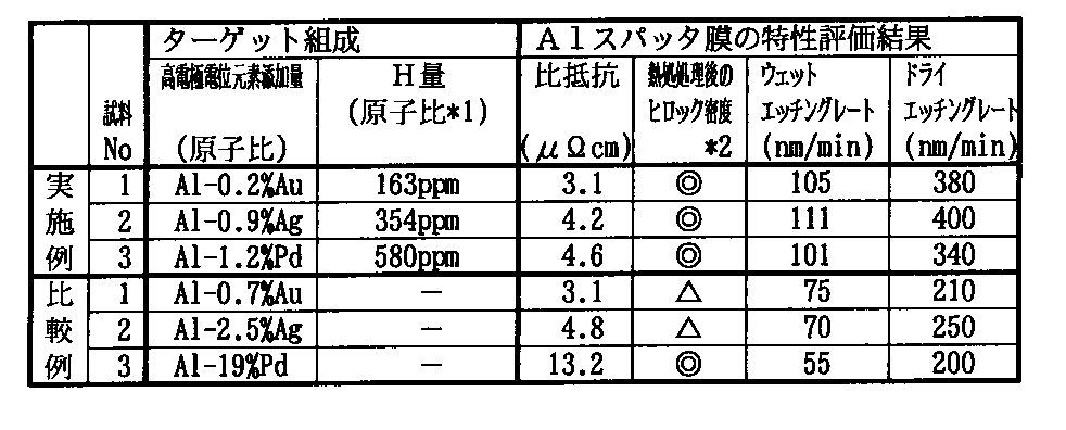
表2に示す各組成のAlスパッタターゲットを、それぞれ実施例1と同様にして作製した後、実施例1と同一条件でスパッタ成膜して、それぞれAl配線膜を得た。これら各Al配線膜の特性を実施例1と同様にして測定、評価した。その結果を併せて表2に示す。
Yに代えて各種元素を用いたAlターゲット(表3に組成を示す)を、それぞれ実施例1と同様にして作製した後、実施例1と同一条件でスパッタ成膜して、それぞれAl配線膜を得た。これら各Al配線膜の特性を実施例1と同様にして測定、評価した。また、試料No16〜21のAl配線膜については、アルカリ溶液中におけるITO電極との反応性も測定、評価した。このアルカリ溶液中におけるITO電極との反応性は、参照電極に銀・塩化銀電極を用いると共に、陽極をITO、陰極を各Al合金とし、通常用いられる電極測定法で調べた。その結果を併せて表3に示す。
まず、Alに対して2.84原子%(6質量%)のCoを添加した原料を、高周波誘導溶解(真空溶解)し、この溶湯内にH2ガスをバブリングしてHを投入した。Hのバブリング量は、インゴット中のH量がCo量に対して980原子ppmとなるように設定した。このようにして作製した目的組成のインゴットに対して、熱間圧延および機械加工を施し、直径127mm×厚さ5mmのAlスパッタターゲットを得た。
表5に示す各組成のAlスパッタターゲットを、それぞれ実施例4と同様にして作製した後、実施例4と同一条件でスパッタ成膜した。このようにして作製した各Al膜をアルカリ溶液(NMD-3/現像液)中に入れ、参照電極(Ag/AgCl/Cl-)を用いて電極電位を測定した。その結果を表5および図8に示す。
Alより標準電極電位が高い元素(Ir、Pt、V、Nb)を用いて、表6に組成を示すAlスパッタターゲットをそれぞれ実施例4と同様にして作製した後、実施例4と同一条件でスパッタ成膜して、それぞれAl配線膜を得た。これら各Al配線膜の特性を実施例1と同様にして測定、評価した。また、これらAl配線膜については、実施例3と同様にして、アルカリ溶液中におけるITO電極との反応性も測定、評価した。その結果を併せて表6に示す。なお、表6中の比較例6は、高電極電位元素の含有量を本発明の範囲外としたものである。
Alより標準電極電位が高い元素(Au、Ag、Pd)を用いて、表7に組成を示すAlスパッタターゲットをそれぞれ実施例4と同様にして作製した後、実施例4と同一条件でスパッタ成膜して、それぞれAl配線膜を得た。これら各Al配線膜の特性を実施例1と同様にして測定、評価した。また、Al配線膜のエッチング性については、ウェットエッチングおよびドライエッチングそれぞれのエッチングレートを調べた。その結果を表7に示す。なお、表7中の比較例7は、Hを添加しない以外は実施例7と同一条件で作製したAlスパッタターゲットを用いて、それぞれ同様にスパッタ成膜したAl膜である。
表8に組成を示すAlスパッタターゲットを、それぞれ実施例4と同様にして作製した後、実施例4と同一条件でスパッタ成膜して、それぞれAl配線膜を得た。これら各Al配線膜の特性を実施例1と同様にして測定、評価した。その結果を表8に示す。
まず、Alに対して0.3原子%(2質量%)のTaを添加した原料を、高周波誘導溶解(真空溶解)し、溶解時にO2をバブリングして酸素を投入した。酸素の投入量は、インゴット中のO量がTa量に対して10原子ppmとなるように設定した。このようにして作製した目的組成のインゴットに対して、熱間圧延および機械加工を施し、直径127mm×厚さ5mmのAlスパッタターゲットを得た。
各種元素を用いたAlターゲット(表10に組成を示す)を、それぞれ実施例9と同様にして作製した後、実施例9と同一条件でスパッタ成膜して、それぞれAl配線膜を得た。これら各Al配線膜の特性を実施例1と同様にして測定、評価した。また、試料No5〜6のAl配線膜については、実施例3と同様にして、アルカリ溶液中におけるITO電極との反応性も測定、評価した。その結果を表10に示す。なお、表10中の比較例10は、添加元素量を本発明の範囲外としたものである。
まず、Alに対して0.28原子%(2質量%)のPtを添加した原料を、高周波誘導溶解(真空溶解)し、溶解時にN2をバブリングして窒素を投入した。窒素の投入量は、インゴット中のN量がPt量に対して19原子ppmとなるように設定した。このようにして作製した目的組成のインゴットに対して、熱間圧延および機械加工を施し、直径127mm×厚さ5mmのAlスパッタターゲットを得た。
各種元素を用いたAlターゲット(表12に組成を示す)を、それぞれ実施例11と同様にして作製した後、実施例11と同一条件でスパッタ成膜して、それぞれAl配線膜を得た。これら各Al配線膜の特性を実施例1と同様にして測定、評価した。なお、表12中の比較例12は、添加元素量を本発明の範囲外としたものである。
Claims (6)
- Y、Sc、La、Ce、Nd、Sm、Gd、Tb、Dy、Er、Th、Sr、Ti、Zr、V、Nb、Ta、Cr、Mo、W、Mn、Tc、Re、Fe、Co、Ni、Pd、Ir、Pt、Cu、Ag、Au、Cd、Si、PbおよびBから選ばれる少なくとも1種の第1の元素を0.001〜30原子%の範囲で含み、残部が実質的にAlからなるインゴットまたは焼結体を、大気溶解法、真空溶解法、急冷凝固法または粉末冶金法で作製するにあたって、O、NおよびHから選ばれる少なくとも1種の第2の元素を含むガスを使用して、前記インゴットまたは焼結体を作製する工程と、
前記インゴットまたは焼結体を加工してスパッタターゲットを作製する工程と
を具備することを特徴とするスパッタターゲットの製造方法。 - 請求項1記載のスパッタターゲットの製造方法において、
前記インゴットまたは焼結体の作製工程に前記大気溶解法または真空溶解法を適用し、かつ溶解中に前記第2の元素を含むガスでバブリングすることを特徴とするスパッタターゲットの製造方法。 - 請求項1記載のスパッタターゲットの製造方法において、
前記インゴットまたは焼結体の作製工程に前記急冷凝固法としてスプレーフォーミング法を適用し、かつスプレー時に前記第2の元素を含むガスを吹き付けることを特徴とするスパッタターゲットの製造方法。 - 請求項1ないし請求項3のいずれか1項記載のスパッタターゲットの製造方法において、
前記インゴットまたは焼結体に前記第2の元素を前記第1の元素量に対して0.01原子ppm〜50原子%の範囲で含有させることを特徴とするスパッタターゲットの製造方法。 - 請求項1ないし請求項3のいずれか1項記載のスパッタターゲットの製造方法において、
前記インゴットまたは焼結体に前記第2の元素を前記第1の元素量に対して0.01原子ppm〜7.5原子%の範囲で含有させることを特徴とするスパッタターゲットの製造方法。 - 請求項1ないし請求項5のいずれか1項記載のスパッタターゲットの製造方法において、
前記第1の元素はAlと金属間化合物を形成する元素であることを特徴とするスパッタターゲットの製造方法。
Priority Applications (1)
| Application Number | Priority Date | Filing Date | Title |
|---|---|---|---|
| JP2005276818A JP4488991B2 (ja) | 1995-10-12 | 2005-09-22 | スパッタターゲットの製造方法 |
Applications Claiming Priority (2)
| Application Number | Priority Date | Filing Date | Title |
|---|---|---|---|
| JP26447295 | 1995-10-12 | ||
| JP2005276818A JP4488991B2 (ja) | 1995-10-12 | 2005-09-22 | スパッタターゲットの製造方法 |
Related Parent Applications (1)
| Application Number | Title | Priority Date | Filing Date |
|---|---|---|---|
| JP51492097A Division JP4137182B2 (ja) | 1995-10-12 | 1996-10-14 | 配線膜形成用スパッタターゲット |
Related Child Applications (1)
| Application Number | Title | Priority Date | Filing Date |
|---|---|---|---|
| JP2009069802A Division JP5175780B2 (ja) | 1995-10-12 | 2009-03-23 | スパッタターゲットの製造方法 |
Publications (2)
| Publication Number | Publication Date |
|---|---|
| JP2006111969A true JP2006111969A (ja) | 2006-04-27 |
| JP4488991B2 JP4488991B2 (ja) | 2010-06-23 |
Family
ID=17403704
Family Applications (7)
| Application Number | Title | Priority Date | Filing Date |
|---|---|---|---|
| JP51492097A Expired - Lifetime JP4137182B2 (ja) | 1995-10-12 | 1996-10-14 | 配線膜形成用スパッタターゲット |
| JP2004076172A Expired - Lifetime JP4130418B2 (ja) | 1995-10-12 | 2004-03-17 | 配線膜とその製造方法、およびそれを用いた電子部品 |
| JP2005276820A Expired - Fee Related JP4589854B2 (ja) | 1995-10-12 | 2005-09-22 | Al合金配線の製造方法 |
| JP2005276819A Expired - Lifetime JP4488992B2 (ja) | 1995-10-12 | 2005-09-22 | スパッタターゲットの製造方法 |
| JP2005276818A Expired - Lifetime JP4488991B2 (ja) | 1995-10-12 | 2005-09-22 | スパッタターゲットの製造方法 |
| JP2009069802A Expired - Lifetime JP5175780B2 (ja) | 1995-10-12 | 2009-03-23 | スパッタターゲットの製造方法 |
| JP2009245733A Expired - Lifetime JP5175824B2 (ja) | 1995-10-12 | 2009-10-26 | スパッタターゲットの製造方法 |
Family Applications Before (4)
| Application Number | Title | Priority Date | Filing Date |
|---|---|---|---|
| JP51492097A Expired - Lifetime JP4137182B2 (ja) | 1995-10-12 | 1996-10-14 | 配線膜形成用スパッタターゲット |
| JP2004076172A Expired - Lifetime JP4130418B2 (ja) | 1995-10-12 | 2004-03-17 | 配線膜とその製造方法、およびそれを用いた電子部品 |
| JP2005276820A Expired - Fee Related JP4589854B2 (ja) | 1995-10-12 | 2005-09-22 | Al合金配線の製造方法 |
| JP2005276819A Expired - Lifetime JP4488992B2 (ja) | 1995-10-12 | 2005-09-22 | スパッタターゲットの製造方法 |
Family Applications After (2)
| Application Number | Title | Priority Date | Filing Date |
|---|---|---|---|
| JP2009069802A Expired - Lifetime JP5175780B2 (ja) | 1995-10-12 | 2009-03-23 | スパッタターゲットの製造方法 |
| JP2009245733A Expired - Lifetime JP5175824B2 (ja) | 1995-10-12 | 2009-10-26 | スパッタターゲットの製造方法 |
Country Status (6)
| Country | Link |
|---|---|
| US (2) | USRE41975E1 (ja) |
| EP (2) | EP1553205B1 (ja) |
| JP (7) | JP4137182B2 (ja) |
| KR (1) | KR100312548B1 (ja) |
| TW (1) | TW318276B (ja) |
| WO (1) | WO1997013885A1 (ja) |
Cited By (6)
| Publication number | Priority date | Publication date | Assignee | Title |
|---|---|---|---|---|
| EP1746173A2 (en) * | 2005-07-22 | 2007-01-24 | Heraeus, Inc. | Enhanced sputter target manufacturing method |
| EP1923481A2 (en) * | 2005-07-22 | 2008-05-21 | Heraeus, Inc. | Enhanced sputter target manufacturing method |
| USRE41975E1 (en) | 1995-10-12 | 2010-11-30 | Kabushiki Kaisha Toshiba | Interconnector line of thin film, sputter target for forming the wiring film and electronic component using the same |
| USRE45481E1 (en) | 1995-10-12 | 2015-04-21 | Kabushiki Kaisha Toshiba | Interconnector line of thin film, sputter target for forming the wiring film and electronic component using the same |
| JP2015096647A (ja) * | 2013-10-08 | 2015-05-21 | 株式会社フルヤ金属 | アルミニウムと希土類元素との合金ターゲット及びその製造方法 |
| KR20210011455A (ko) * | 2018-06-28 | 2021-02-01 | 가부시키가이샤 아루박 | 알루미늄 합금 타깃 및 그 제조방법 |
Families Citing this family (78)
| Publication number | Priority date | Publication date | Assignee | Title |
|---|---|---|---|---|
| JPH10142625A (ja) * | 1996-11-07 | 1998-05-29 | Vacuum Metallurgical Co Ltd | 液晶ディスプレイの導電部製作方法及びその製作に用いるスパッタリングターゲット |
| TW574394B (en) * | 1997-07-15 | 2004-02-01 | Micron Technology Inc | Method of using hydrogen and oxygen gas in sputter deposition of aluminum-containing films and aluminum-containing films derived therefrom |
| US6222271B1 (en) | 1997-07-15 | 2001-04-24 | Micron Technology, Inc. | Method of using hydrogen gas in sputter deposition of aluminum-containing films and aluminum-containing films derived therefrom |
| US5969423A (en) | 1997-07-15 | 1999-10-19 | Micron Technology, Inc. | Aluminum-containing films derived from using hydrogen and oxygen gas in sputter deposition |
| US6448708B1 (en) | 1997-09-17 | 2002-09-10 | Candescent Intellectual Property Services, Inc. | Dual-layer metal for flat panel display |
| US6736947B1 (en) | 1997-12-24 | 2004-05-18 | Kabushiki Kaisha Toshiba | Sputtering target, A1 interconnection film, and electronic component |
| US6710525B1 (en) | 1999-10-19 | 2004-03-23 | Candescent Technologies Corporation | Electrode structure and method for forming electrode structure for a flat panel display |
| EP1698714B1 (en) | 2000-12-28 | 2009-09-02 | Kabushiki Kaisha Kobe Seiko Sho | Target used to form a hard film |
| JP2002373867A (ja) * | 2001-06-14 | 2002-12-26 | Idemitsu Kosan Co Ltd | 半導体素子用導電性薄膜、半導体素子及びそれらの製造方法 |
| JP2003089864A (ja) * | 2001-09-18 | 2003-03-28 | Mitsui Mining & Smelting Co Ltd | アルミニウム合金薄膜及びその薄膜を有する配線回路並びにその薄膜を形成するターゲット材 |
| KR20040077797A (ko) * | 2002-01-24 | 2004-09-06 | 허니웰 인터내셔널 인코포레이티드 | 박막, 박막을 갖는 구조, 및 박막을 형성하는 방법 |
| JP2004143584A (ja) * | 2002-08-29 | 2004-05-20 | Nippon Sheet Glass Co Ltd | ジルコニウム化合物膜が被覆された物品、その物品の製造方法及びその膜を被覆するために用いるスパッタリングターゲット |
| EP1411146B1 (en) * | 2002-10-17 | 2010-06-09 | Samsung Electronics Co., Ltd. | Method of forming cobalt silicide film and method of manufacturing semiconductor device having cobalt silicide film |
| JP3940385B2 (ja) | 2002-12-19 | 2007-07-04 | 株式会社神戸製鋼所 | 表示デバイスおよびその製法 |
| JP2006339666A (ja) * | 2002-12-19 | 2006-12-14 | Kobe Steel Ltd | アルミニウム合金膜形成用スパッタリングターゲット |
| CN1307694C (zh) * | 2003-06-03 | 2007-03-28 | 旺宏电子股份有限公司 | 降低半导体组件中二硅化钴层的电阻值的方法 |
| US7030430B2 (en) * | 2003-08-15 | 2006-04-18 | Intel Corporation | Transition metal alloys for use as a gate electrode and devices incorporating these alloys |
| JP2005086118A (ja) * | 2003-09-11 | 2005-03-31 | Renesas Technology Corp | 半導体装置 |
| US20070102822A1 (en) * | 2003-12-18 | 2007-05-10 | Takashi Kubota | Aluminum base target and process for producing the same |
| EP1557863B1 (en) * | 2004-01-22 | 2011-12-21 | Canon Kabushiki Kaisha | Antistatic film, spacer using it and picture display unit |
| CN1918672B (zh) * | 2004-03-09 | 2012-10-03 | 出光兴产株式会社 | 薄膜晶体管、薄膜晶体管基板、液晶显示装置、溅射靶、透明导电膜、透明电极及它们的制造方法 |
| CN100417993C (zh) * | 2004-03-25 | 2008-09-10 | 三井金属鉱业株式会社 | 薄膜电路的接合结构 |
| JP4646912B2 (ja) * | 2004-03-25 | 2011-03-09 | 三井金属鉱業株式会社 | 薄膜回路の接合構造 |
| JP4849821B2 (ja) * | 2004-04-28 | 2012-01-11 | 株式会社半導体エネルギー研究所 | 表示装置、電子機器 |
| US7550769B2 (en) * | 2004-06-11 | 2009-06-23 | Semiconductor Energy Laboratory Co., Ltd. | Light emitting element, light emitting device and semiconductor device |
| JP5060714B2 (ja) | 2004-09-30 | 2012-10-31 | 株式会社神戸製鋼所 | 耐摩耗性および耐酸化性に優れた硬質皮膜、並びに該硬質皮膜形成用ターゲット |
| WO2006057312A1 (ja) * | 2004-11-24 | 2006-06-01 | Tosoh Corporation | 配線・電極及びスパッタリングターゲット |
| US7531904B2 (en) * | 2005-04-26 | 2009-05-12 | Mitsui Mining & Smelting Co., Ltd. | Al-Ni-B alloy wiring material and element structure using the same |
| WO2006117884A1 (ja) * | 2005-04-26 | 2006-11-09 | Mitsui Mining & Smelting Co., Ltd. | Al-Ni-B合金配線材料及びそれを用いた素子構造 |
| JP4117002B2 (ja) * | 2005-12-02 | 2008-07-09 | 株式会社神戸製鋼所 | 薄膜トランジスタ基板および表示デバイス |
| JP2007191761A (ja) * | 2006-01-19 | 2007-08-02 | Idemitsu Kosan Co Ltd | 積層構造、それを用いた電気回路用電極及びその製造方法 |
| US20090008786A1 (en) | 2006-03-06 | 2009-01-08 | Tosoh Smd, Inc. | Sputtering Target |
| KR20080100358A (ko) * | 2006-03-06 | 2008-11-17 | 토소우 에스엠디, 인크 | 전자 장치, 이의 제조방법 및 스퍼터링 타겟 |
| JP4728170B2 (ja) * | 2006-05-26 | 2011-07-20 | 三菱電機株式会社 | 半導体デバイスおよびアクティブマトリクス型表示装置 |
| JP5234892B2 (ja) * | 2006-05-31 | 2013-07-10 | 株式会社神戸製鋼所 | 薄膜トランジスタ基板および表示デバイス |
| CN101365816B (zh) * | 2006-10-16 | 2010-10-06 | 三井金属鉱业株式会社 | 反射膜用Al-Ni-B合金材料 |
| WO2008050710A1 (en) * | 2006-10-26 | 2008-05-02 | Mitsui Mining & Smelting Co., Ltd. | Al-BASE ALLOY WIRING MATERIAL AND ELEMENT STRUCTURE USING THE SAME |
| JP4377906B2 (ja) * | 2006-11-20 | 2009-12-02 | 株式会社コベルコ科研 | Al−Ni−La系Al基合金スパッタリングターゲット、およびその製造方法 |
| WO2008066030A1 (en) * | 2006-11-30 | 2008-06-05 | Kabushiki Kaisha Kobe Seiko Sho | Al ALLOY FILM FOR DISPLAY DEVICE, DISPLAY DEVICE, AND SPUTTERING TARGET |
| JP4170367B2 (ja) | 2006-11-30 | 2008-10-22 | 株式会社神戸製鋼所 | 表示デバイス用Al合金膜、表示デバイス、及びスパッタリングターゲット |
| KR100818525B1 (ko) * | 2006-12-20 | 2008-03-31 | 동부일렉트로닉스 주식회사 | 이미지 센서 및 그의 제조방법 |
| KR100853545B1 (ko) | 2007-05-15 | 2008-08-21 | 삼성에스디아이 주식회사 | 유기전계발광소자 및 그의 제조방법 |
| JP2009008770A (ja) | 2007-06-26 | 2009-01-15 | Kobe Steel Ltd | 積層構造およびその製造方法 |
| JP2009010052A (ja) * | 2007-06-26 | 2009-01-15 | Kobe Steel Ltd | 表示装置の製造方法 |
| JP5143649B2 (ja) * | 2007-07-24 | 2013-02-13 | 株式会社コベルコ科研 | Al−Ni−La−Si系Al合金スパッタリングターゲットおよびその製造方法 |
| JP2009076536A (ja) | 2007-09-19 | 2009-04-09 | Mitsubishi Electric Corp | Al合金膜、電子デバイス及び電気光学表示装置用アクティブマトリックス基板 |
| US20110008640A1 (en) * | 2008-03-31 | 2011-01-13 | Kabushiki Kaisha Kobe Seiko Sho (Kobe Steel Ltd.) | Display device, process for producing the display device, and sputtering target |
| JP5308760B2 (ja) * | 2008-09-30 | 2013-10-09 | 株式会社日立製作所 | 表示装置 |
| CN102473644A (zh) * | 2009-07-31 | 2012-05-23 | 国立大学法人东北大学 | 半导体装置、半导体装置的制造方法、以及显示装置 |
| WO2011058867A1 (en) * | 2009-11-13 | 2011-05-19 | Semiconductor Energy Laboratory Co., Ltd. | Sputtering target and method for manufacturing the same, and transistor |
| WO2011058882A1 (en) * | 2009-11-13 | 2011-05-19 | Semiconductor Energy Laboratory Co., Ltd. | Sputtering target and manufacturing method thereof, and transistor |
| WO2011068037A1 (en) | 2009-12-04 | 2011-06-09 | Semiconductor Energy Laboratory Co., Ltd. | Semiconductor device and manufacturing method thereof |
| TW201140627A (en) * | 2010-05-05 | 2011-11-16 | Univ Nat Yunlin Sci & Tech | Method for producing aluminum foil electrode of carbon nano-tube |
| JP5032687B2 (ja) * | 2010-09-30 | 2012-09-26 | 株式会社神戸製鋼所 | Al合金膜、Al合金膜を有する配線構造、およびAl合金膜の製造に用いられるスパッタリングターゲット |
| US8894825B2 (en) | 2010-12-17 | 2014-11-25 | Semiconductor Energy Laboratory Co., Ltd. | Sputtering target, method for manufacturing the same, manufacturing semiconductor device |
| JP5909852B2 (ja) * | 2011-02-23 | 2016-04-27 | ソニー株式会社 | 半導体装置の製造方法 |
| JP2012186199A (ja) * | 2011-03-03 | 2012-09-27 | Toshiba Corp | 半導体発光装置およびその製造方法 |
| CN103952604B (zh) * | 2014-04-10 | 2016-06-08 | 安徽银力铸造有限公司 | 一种汽车用防锈铝合金 |
| CN104451281A (zh) * | 2014-12-25 | 2015-03-25 | 春焱电子科技(苏州)有限公司 | 一种电子材料用铝合金 |
| WO2016186070A1 (ja) * | 2015-05-21 | 2016-11-24 | Jx金属株式会社 | 銅合金スパッタリングターゲット及びその製造方法 |
| EP3184669B1 (en) * | 2015-12-23 | 2018-07-18 | ATOTECH Deutschland GmbH | Etching solution for copper and copper alloy surfaces |
| JP6574714B2 (ja) * | 2016-01-25 | 2019-09-11 | 株式会社コベルコ科研 | 配線構造およびスパッタリングターゲット |
| CN105586576A (zh) * | 2016-02-04 | 2016-05-18 | 东莞沙头朝日五金电子制品有限公司 | 一种镀制pvd防菌膜的方法 |
| JP6869237B2 (ja) * | 2016-06-07 | 2021-05-12 | Jx金属株式会社 | スパッタリングターゲット及び、その製造方法 |
| CN106555083B (zh) * | 2016-12-05 | 2018-03-20 | 合肥工业大学 | 一种全铝合金架空导线及其制备方法 |
| CN106521250B (zh) * | 2016-12-05 | 2018-03-20 | 合肥工业大学 | 一种大载流耐热铝合金导线的制备方法 |
| TWI752189B (zh) * | 2017-03-13 | 2022-01-11 | 美商萬騰榮公司 | 具高元素含量的鋁合金及製品 |
| US10760156B2 (en) | 2017-10-13 | 2020-09-01 | Honeywell International Inc. | Copper manganese sputtering target |
| US11035036B2 (en) | 2018-02-01 | 2021-06-15 | Honeywell International Inc. | Method of forming copper alloy sputtering targets with refined shape and microstructure |
| CN108396205B (zh) * | 2018-04-28 | 2020-09-04 | 广州致远新材料科技有限公司 | 一种铝合金材料及其制备方法 |
| CN112262222B (zh) * | 2018-06-28 | 2023-06-06 | 株式会社爱发科 | 铝合金膜、其制造方法以及薄膜晶体管 |
| JP7096291B2 (ja) * | 2019-11-26 | 2022-07-05 | 株式会社フルヤ金属 | スパッタリングターゲット |
| EP4006197A4 (en) * | 2019-07-31 | 2023-08-16 | Furuya Metal Co., Ltd. | SPUTTER TARGET |
| CN110923529A (zh) * | 2019-11-29 | 2020-03-27 | 安徽峰创云通数据科技有限公司 | 电力电缆用Al-Cu-Sr-RE-Ge铝合金线及其制备方法 |
| KR102329427B1 (ko) * | 2020-01-03 | 2021-11-24 | 와이엠씨 주식회사 | 배선전극용 합금 조성물 및 그의 제조방법 |
| KR102329426B1 (ko) * | 2020-01-03 | 2021-11-24 | 와이엠씨 주식회사 | 배선전극용 합금 조성물 및 그의 제조방법 |
| WO2022004491A1 (ja) * | 2020-06-30 | 2022-01-06 | 株式会社アルバック | 金属配線構造体、金属配線構造体の製造方法及びスパッタリングターゲット |
| WO2023189074A1 (ja) * | 2022-03-29 | 2023-10-05 | 株式会社村田製作所 | 弾性波装置 |
Family Cites Families (25)
| Publication number | Priority date | Publication date | Assignee | Title |
|---|---|---|---|---|
| US4302498A (en) * | 1980-10-28 | 1981-11-24 | Rca Corporation | Laminated conducting film on an integrated circuit substrate and method of forming the laminate |
| JPS62228446A (ja) * | 1985-11-29 | 1987-10-07 | Nippon Mining Co Ltd | 半導体配線材料用アルミニウム合金 |
| JPH0656883B2 (ja) | 1986-03-03 | 1994-07-27 | 鐘淵化学工業株式会社 | 半導体装置 |
| JPS62235454A (ja) * | 1986-04-03 | 1987-10-15 | Nippon Mining Co Ltd | 半導体配線材料用N含有Al合金 |
| JPS62240738A (ja) | 1986-04-11 | 1987-10-21 | Nippon Mining Co Ltd | 半導体配線材料用n、c含有アルミニウム合金 |
| JPH0768612B2 (ja) | 1987-04-20 | 1995-07-26 | 日立金属株式会社 | 希土類金属―鉄族金属ターゲット用合金粉末、希土類金属―鉄族金属ターゲット、およびそれらの製造方法 |
| JPS6425977U (ja) | 1987-08-07 | 1989-02-14 | ||
| JPS6457965A (en) * | 1987-08-27 | 1989-03-06 | Sumitomo Electric Industries | Production of spiral part by spray forming of aluminum alloy |
| JPH0649933B2 (ja) * | 1987-09-18 | 1994-06-29 | 日本鋼管株式会社 | 缶用めっき鋼板 |
| JPH01134426A (ja) | 1987-11-20 | 1989-05-26 | Hitachi Ltd | 液晶デイスプレイ駆動用薄膜トランジスタ |
| JP2597380B2 (ja) | 1988-03-23 | 1997-04-02 | 日立金属株式会社 | 希土類金属−遷移金属ターゲット用合金粉末の製造方法および希土類金属−遷移金属ターゲットの製造方法 |
| JP2714606B2 (ja) | 1988-05-16 | 1998-02-16 | 日本電信電話株式会社 | 配線層及びその製法 |
| DE3911657A1 (de) * | 1989-04-10 | 1990-10-11 | Telefunken Electronic Gmbh | Halbleiter-bauelement |
| US5367179A (en) | 1990-04-25 | 1994-11-22 | Casio Computer Co., Ltd. | Thin-film transistor having electrodes made of aluminum, and an active matrix panel using same |
| JP3282204B2 (ja) * | 1991-12-24 | 2002-05-13 | カシオ計算機株式会社 | アルミニウム系合金膜の成膜方法 |
| JPH0441063A (ja) * | 1990-06-06 | 1992-02-12 | Nkk Corp | スプレーフォーミング法 |
| JPH0448854A (ja) * | 1990-06-15 | 1992-02-18 | Sharp Corp | データ通信設備装置 |
| JP3061654B2 (ja) | 1991-04-23 | 2000-07-10 | 株式会社神戸製鋼所 | 液晶ディスプレイ用半導体装置材料及び液晶ディスプレイ用半導体装置材料製造用溶製スパッタリングターゲット材料 |
| JP3021996B2 (ja) | 1991-09-30 | 2000-03-15 | 松下電器産業株式会社 | アルミニウム配線およびその形成方法 |
| US5211824A (en) * | 1991-10-31 | 1993-05-18 | Siemens Solar Industries L.P. | Method and apparatus for sputtering of a liquid |
| EP0542271B1 (en) * | 1991-11-15 | 1998-01-14 | Casio Computer Company Limited | Thin-film device with a compound conductive layer |
| JPH05239635A (ja) * | 1992-02-26 | 1993-09-17 | Shimadzu Corp | 透明導電膜の製造方法 |
| JP2733006B2 (ja) * | 1993-07-27 | 1998-03-30 | 株式会社神戸製鋼所 | 半導体用電極及びその製造方法並びに半導体用電極膜形成用スパッタリングターゲット |
| JPH07246452A (ja) * | 1994-03-09 | 1995-09-26 | Kobe Steel Ltd | 噴霧成形法 |
| EP1553205B1 (en) | 1995-10-12 | 2017-01-25 | Kabushiki Kaisha Toshiba | Sputter target for forming thin film interconnector and thin film interconnector line |
-
1996
- 1996-10-14 EP EP05003598.9A patent/EP1553205B1/en not_active Expired - Lifetime
- 1996-10-14 JP JP51492097A patent/JP4137182B2/ja not_active Expired - Lifetime
- 1996-10-14 EP EP96933629A patent/EP0855451A4/en not_active Withdrawn
- 1996-10-14 US US10/732,888 patent/USRE41975E1/en not_active Expired - Lifetime
- 1996-10-14 KR KR1019980702718A patent/KR100312548B1/ko active IP Right Grant
- 1996-10-14 US US09/051,567 patent/US6329275B1/en not_active Ceased
- 1996-10-14 WO PCT/JP1996/002961 patent/WO1997013885A1/ja not_active Application Discontinuation
- 1996-11-28 TW TW085114794A patent/TW318276B/zh not_active IP Right Cessation
-
2004
- 2004-03-17 JP JP2004076172A patent/JP4130418B2/ja not_active Expired - Lifetime
-
2005
- 2005-09-22 JP JP2005276820A patent/JP4589854B2/ja not_active Expired - Fee Related
- 2005-09-22 JP JP2005276819A patent/JP4488992B2/ja not_active Expired - Lifetime
- 2005-09-22 JP JP2005276818A patent/JP4488991B2/ja not_active Expired - Lifetime
-
2009
- 2009-03-23 JP JP2009069802A patent/JP5175780B2/ja not_active Expired - Lifetime
- 2009-10-26 JP JP2009245733A patent/JP5175824B2/ja not_active Expired - Lifetime
Cited By (9)
| Publication number | Priority date | Publication date | Assignee | Title |
|---|---|---|---|---|
| USRE41975E1 (en) | 1995-10-12 | 2010-11-30 | Kabushiki Kaisha Toshiba | Interconnector line of thin film, sputter target for forming the wiring film and electronic component using the same |
| USRE45481E1 (en) | 1995-10-12 | 2015-04-21 | Kabushiki Kaisha Toshiba | Interconnector line of thin film, sputter target for forming the wiring film and electronic component using the same |
| EP1746173A2 (en) * | 2005-07-22 | 2007-01-24 | Heraeus, Inc. | Enhanced sputter target manufacturing method |
| EP1746173A3 (en) * | 2005-07-22 | 2007-05-09 | Heraeus, Inc. | Enhanced sputter target manufacturing method |
| EP1923481A2 (en) * | 2005-07-22 | 2008-05-21 | Heraeus, Inc. | Enhanced sputter target manufacturing method |
| EP1923481A3 (en) * | 2005-07-22 | 2008-06-18 | Heraeus, Inc. | Enhanced sputter target manufacturing method |
| JP2015096647A (ja) * | 2013-10-08 | 2015-05-21 | 株式会社フルヤ金属 | アルミニウムと希土類元素との合金ターゲット及びその製造方法 |
| KR20210011455A (ko) * | 2018-06-28 | 2021-02-01 | 가부시키가이샤 아루박 | 알루미늄 합금 타깃 및 그 제조방법 |
| KR102571458B1 (ko) | 2018-06-28 | 2023-08-25 | 가부시키가이샤 아루박 | 알루미늄 합금 타깃 및 그 제조방법 |
Also Published As
| Publication number | Publication date |
|---|---|
| EP0855451A1 (en) | 1998-07-29 |
| JP5175824B2 (ja) | 2013-04-03 |
| EP1553205A1 (en) | 2005-07-13 |
| USRE41975E1 (en) | 2010-11-30 |
| JP5175780B2 (ja) | 2013-04-03 |
| EP0855451A4 (en) | 1999-10-06 |
| US6329275B1 (en) | 2001-12-11 |
| JP4589854B2 (ja) | 2010-12-01 |
| KR19990064231A (ko) | 1999-07-26 |
| JP2010031378A (ja) | 2010-02-12 |
| JP4488992B2 (ja) | 2010-06-23 |
| JP4130418B2 (ja) | 2008-08-06 |
| KR100312548B1 (ko) | 2001-12-28 |
| TW318276B (ja) | 1997-10-21 |
| JP4488991B2 (ja) | 2010-06-23 |
| JP2004260194A (ja) | 2004-09-16 |
| EP1553205B1 (en) | 2017-01-25 |
| JP2006111970A (ja) | 2006-04-27 |
| JP2006100822A (ja) | 2006-04-13 |
| WO1997013885A1 (en) | 1997-04-17 |
| JP2009149997A (ja) | 2009-07-09 |
| JP4137182B2 (ja) | 2008-08-20 |
Similar Documents
| Publication | Publication Date | Title |
|---|---|---|
| JP4488991B2 (ja) | スパッタターゲットの製造方法 | |
| JP4065959B2 (ja) | 液晶表示装置、スパッタリングターゲット材および銅合金 | |
| US8350303B2 (en) | Display device and sputtering target for producing the same | |
| JP3132310B2 (ja) | アクティブマトリクス型液晶表示装置 | |
| JP2003017706A (ja) | Tft基板、それを用いた液晶表示装置及びその製造方法 | |
| JP2019102896A (ja) | アルミニウム合金膜 | |
| JPH09199976A (ja) | 弾性表面波素子電極 | |
| JP4031764B2 (ja) | 弾性表面波素子、弾性表面波装置、デュプレクサ及び弾性表面波素子の製造方法 | |
| JP3365978B2 (ja) | 半導体デバイス電極用Al合金薄膜及び半導体デバイス電極用Al合金薄膜形成用のスパッタリングターゲット | |
| USRE45481E1 (en) | Interconnector line of thin film, sputter target for forming the wiring film and electronic component using the same | |
| JP2534434B2 (ja) | 耐酸化性化合物およびその製造方法 | |
| US6965190B2 (en) | Surface acoustic wave device | |
| JP3168400B2 (ja) | 半導体装置および半導体装置の製造方法 | |
| JPH06196526A (ja) | 半導体装置の製造方法 | |
| JP3256953B2 (ja) | モノリシック圧電フィルタ | |
| JPH08250452A (ja) | 半導体装置及びその製造方法 | |
| JPH10125619A (ja) | 配線層および配線層の形成方法 | |
| JPH09199968A (ja) | 弾性表面波素子用薄膜電極及びその形成方法 | |
| JPH09228035A (ja) | 薄膜配線用Al合金膜およびAl合金スパッタリングターゲット材 | |
| JP2002353767A (ja) | 弾性表面波装置 | |
| CN115485818A (zh) | 金属布线结构体、金属布线结构体的制造方法及溅射靶 | |
| JPS5810009B2 (ja) | 弾性表面波素子の製造方法 | |
| JP2001324724A (ja) | 液晶表示装置 | |
| JP2004289441A (ja) | 弾性表面波素子およびその製造方法 | |
| JP2001154224A (ja) | アクティブマトリクス型液晶表示装置 |
Legal Events
| Date | Code | Title | Description |
|---|---|---|---|
| A131 | Notification of reasons for refusal |
Free format text: JAPANESE INTERMEDIATE CODE: A131 Effective date: 20090120 |
|
| A521 | Request for written amendment filed |
Free format text: JAPANESE INTERMEDIATE CODE: A523 Effective date: 20090323 |
|
| A02 | Decision of refusal |
Free format text: JAPANESE INTERMEDIATE CODE: A02 Effective date: 20090825 |
|
| A521 | Request for written amendment filed |
Free format text: JAPANESE INTERMEDIATE CODE: A523 Effective date: 20091118 |
|
| A911 | Transfer to examiner for re-examination before appeal (zenchi) |
Free format text: JAPANESE INTERMEDIATE CODE: A911 Effective date: 20100105 |
|
| TRDD | Decision of grant or rejection written | ||
| A01 | Written decision to grant a patent or to grant a registration (utility model) |
Free format text: JAPANESE INTERMEDIATE CODE: A01 Effective date: 20100302 |
|
| A01 | Written decision to grant a patent or to grant a registration (utility model) |
Free format text: JAPANESE INTERMEDIATE CODE: A01 |
|
| A61 | First payment of annual fees (during grant procedure) |
Free format text: JAPANESE INTERMEDIATE CODE: A61 Effective date: 20100330 |
|
| FPAY | Renewal fee payment (event date is renewal date of database) |
Free format text: PAYMENT UNTIL: 20130409 Year of fee payment: 3 |
|
| FPAY | Renewal fee payment (event date is renewal date of database) |
Free format text: PAYMENT UNTIL: 20130409 Year of fee payment: 3 |
|
| FPAY | Renewal fee payment (event date is renewal date of database) |
Free format text: PAYMENT UNTIL: 20140409 Year of fee payment: 4 |
|
| EXPY | Cancellation because of completion of term |