JP2006111969A - Sputter target manufacturing method - Google Patents
Sputter target manufacturing method Download PDFInfo
- Publication number
- JP2006111969A JP2006111969A JP2005276818A JP2005276818A JP2006111969A JP 2006111969 A JP2006111969 A JP 2006111969A JP 2005276818 A JP2005276818 A JP 2005276818A JP 2005276818 A JP2005276818 A JP 2005276818A JP 2006111969 A JP2006111969 A JP 2006111969A
- Authority
- JP
- Japan
- Prior art keywords
- wiring
- film
- sputter target
- manufacturing
- ingot
- Prior art date
- Legal status (The legal status is an assumption and is not a legal conclusion. Google has not performed a legal analysis and makes no representation as to the accuracy of the status listed.)
- Granted
Links
Images


Classifications
-
- H—ELECTRICITY
- H01—ELECTRIC ELEMENTS
- H01L—SEMICONDUCTOR DEVICES NOT COVERED BY CLASS H10
- H01L21/00—Processes or apparatus adapted for the manufacture or treatment of semiconductor or solid state devices or of parts thereof
- H01L21/02—Manufacture or treatment of semiconductor devices or of parts thereof
- H01L21/04—Manufacture or treatment of semiconductor devices or of parts thereof the devices having at least one potential-jump barrier or surface barrier, e.g. PN junction, depletion layer or carrier concentration layer
- H01L21/18—Manufacture or treatment of semiconductor devices or of parts thereof the devices having at least one potential-jump barrier or surface barrier, e.g. PN junction, depletion layer or carrier concentration layer the devices having semiconductor bodies comprising elements of Group IV of the Periodic System or AIIIBV compounds with or without impurities, e.g. doping materials
- H01L21/30—Treatment of semiconductor bodies using processes or apparatus not provided for in groups H01L21/20 - H01L21/26
- H01L21/31—Treatment of semiconductor bodies using processes or apparatus not provided for in groups H01L21/20 - H01L21/26 to form insulating layers thereon, e.g. for masking or by using photolithographic techniques; After treatment of these layers; Selection of materials for these layers
- H01L21/3205—Deposition of non-insulating-, e.g. conductive- or resistive-, layers on insulating layers; After-treatment of these layers
- H01L21/32051—Deposition of metallic or metal-silicide layers
-
- C—CHEMISTRY; METALLURGY
- C23—COATING METALLIC MATERIAL; COATING MATERIAL WITH METALLIC MATERIAL; CHEMICAL SURFACE TREATMENT; DIFFUSION TREATMENT OF METALLIC MATERIAL; COATING BY VACUUM EVAPORATION, BY SPUTTERING, BY ION IMPLANTATION OR BY CHEMICAL VAPOUR DEPOSITION, IN GENERAL; INHIBITING CORROSION OF METALLIC MATERIAL OR INCRUSTATION IN GENERAL
- C23C—COATING METALLIC MATERIAL; COATING MATERIAL WITH METALLIC MATERIAL; SURFACE TREATMENT OF METALLIC MATERIAL BY DIFFUSION INTO THE SURFACE, BY CHEMICAL CONVERSION OR SUBSTITUTION; COATING BY VACUUM EVAPORATION, BY SPUTTERING, BY ION IMPLANTATION OR BY CHEMICAL VAPOUR DEPOSITION, IN GENERAL
- C23C14/00—Coating by vacuum evaporation, by sputtering or by ion implantation of the coating forming material
- C23C14/06—Coating by vacuum evaporation, by sputtering or by ion implantation of the coating forming material characterised by the coating material
- C23C14/14—Metallic material, boron or silicon
-
- C—CHEMISTRY; METALLURGY
- C22—METALLURGY; FERROUS OR NON-FERROUS ALLOYS; TREATMENT OF ALLOYS OR NON-FERROUS METALS
- C22C—ALLOYS
- C22C21/00—Alloys based on aluminium
-
- C—CHEMISTRY; METALLURGY
- C23—COATING METALLIC MATERIAL; COATING MATERIAL WITH METALLIC MATERIAL; CHEMICAL SURFACE TREATMENT; DIFFUSION TREATMENT OF METALLIC MATERIAL; COATING BY VACUUM EVAPORATION, BY SPUTTERING, BY ION IMPLANTATION OR BY CHEMICAL VAPOUR DEPOSITION, IN GENERAL; INHIBITING CORROSION OF METALLIC MATERIAL OR INCRUSTATION IN GENERAL
- C23C—COATING METALLIC MATERIAL; COATING MATERIAL WITH METALLIC MATERIAL; SURFACE TREATMENT OF METALLIC MATERIAL BY DIFFUSION INTO THE SURFACE, BY CHEMICAL CONVERSION OR SUBSTITUTION; COATING BY VACUUM EVAPORATION, BY SPUTTERING, BY ION IMPLANTATION OR BY CHEMICAL VAPOUR DEPOSITION, IN GENERAL
- C23C14/00—Coating by vacuum evaporation, by sputtering or by ion implantation of the coating forming material
- C23C14/06—Coating by vacuum evaporation, by sputtering or by ion implantation of the coating forming material characterised by the coating material
- C23C14/14—Metallic material, boron or silicon
- C23C14/16—Metallic material, boron or silicon on metallic substrates or on substrates of boron or silicon
- C23C14/165—Metallic material, boron or silicon on metallic substrates or on substrates of boron or silicon by cathodic sputtering
-
- C—CHEMISTRY; METALLURGY
- C23—COATING METALLIC MATERIAL; COATING MATERIAL WITH METALLIC MATERIAL; CHEMICAL SURFACE TREATMENT; DIFFUSION TREATMENT OF METALLIC MATERIAL; COATING BY VACUUM EVAPORATION, BY SPUTTERING, BY ION IMPLANTATION OR BY CHEMICAL VAPOUR DEPOSITION, IN GENERAL; INHIBITING CORROSION OF METALLIC MATERIAL OR INCRUSTATION IN GENERAL
- C23C—COATING METALLIC MATERIAL; COATING MATERIAL WITH METALLIC MATERIAL; SURFACE TREATMENT OF METALLIC MATERIAL BY DIFFUSION INTO THE SURFACE, BY CHEMICAL CONVERSION OR SUBSTITUTION; COATING BY VACUUM EVAPORATION, BY SPUTTERING, BY ION IMPLANTATION OR BY CHEMICAL VAPOUR DEPOSITION, IN GENERAL
- C23C14/00—Coating by vacuum evaporation, by sputtering or by ion implantation of the coating forming material
- C23C14/22—Coating by vacuum evaporation, by sputtering or by ion implantation of the coating forming material characterised by the process of coating
- C23C14/34—Sputtering
- C23C14/3407—Cathode assembly for sputtering apparatus, e.g. Target
- C23C14/3414—Metallurgical or chemical aspects of target preparation, e.g. casting, powder metallurgy
-
- H—ELECTRICITY
- H01—ELECTRIC ELEMENTS
- H01L—SEMICONDUCTOR DEVICES NOT COVERED BY CLASS H10
- H01L21/00—Processes or apparatus adapted for the manufacture or treatment of semiconductor or solid state devices or of parts thereof
- H01L21/02—Manufacture or treatment of semiconductor devices or of parts thereof
- H01L21/04—Manufacture or treatment of semiconductor devices or of parts thereof the devices having at least one potential-jump barrier or surface barrier, e.g. PN junction, depletion layer or carrier concentration layer
- H01L21/18—Manufacture or treatment of semiconductor devices or of parts thereof the devices having at least one potential-jump barrier or surface barrier, e.g. PN junction, depletion layer or carrier concentration layer the devices having semiconductor bodies comprising elements of Group IV of the Periodic System or AIIIBV compounds with or without impurities, e.g. doping materials
- H01L21/28—Manufacture of electrodes on semiconductor bodies using processes or apparatus not provided for in groups H01L21/20 - H01L21/268
- H01L21/283—Deposition of conductive or insulating materials for electrodes conducting electric current
- H01L21/285—Deposition of conductive or insulating materials for electrodes conducting electric current from a gas or vapour, e.g. condensation
- H01L21/28506—Deposition of conductive or insulating materials for electrodes conducting electric current from a gas or vapour, e.g. condensation of conductive layers
- H01L21/28512—Deposition of conductive or insulating materials for electrodes conducting electric current from a gas or vapour, e.g. condensation of conductive layers on semiconductor bodies comprising elements of Group IV of the Periodic System
- H01L21/2855—Deposition of conductive or insulating materials for electrodes conducting electric current from a gas or vapour, e.g. condensation of conductive layers on semiconductor bodies comprising elements of Group IV of the Periodic System by physical means, e.g. sputtering, evaporation
-
- H—ELECTRICITY
- H01—ELECTRIC ELEMENTS
- H01L—SEMICONDUCTOR DEVICES NOT COVERED BY CLASS H10
- H01L21/00—Processes or apparatus adapted for the manufacture or treatment of semiconductor or solid state devices or of parts thereof
- H01L21/02—Manufacture or treatment of semiconductor devices or of parts thereof
- H01L21/04—Manufacture or treatment of semiconductor devices or of parts thereof the devices having at least one potential-jump barrier or surface barrier, e.g. PN junction, depletion layer or carrier concentration layer
- H01L21/18—Manufacture or treatment of semiconductor devices or of parts thereof the devices having at least one potential-jump barrier or surface barrier, e.g. PN junction, depletion layer or carrier concentration layer the devices having semiconductor bodies comprising elements of Group IV of the Periodic System or AIIIBV compounds with or without impurities, e.g. doping materials
- H01L21/30—Treatment of semiconductor bodies using processes or apparatus not provided for in groups H01L21/20 - H01L21/26
- H01L21/31—Treatment of semiconductor bodies using processes or apparatus not provided for in groups H01L21/20 - H01L21/26 to form insulating layers thereon, e.g. for masking or by using photolithographic techniques; After treatment of these layers; Selection of materials for these layers
- H01L21/3205—Deposition of non-insulating-, e.g. conductive- or resistive-, layers on insulating layers; After-treatment of these layers
-
- H—ELECTRICITY
- H01—ELECTRIC ELEMENTS
- H01L—SEMICONDUCTOR DEVICES NOT COVERED BY CLASS H10
- H01L23/00—Details of semiconductor or other solid state devices
- H01L23/52—Arrangements for conducting electric current within the device in operation from one component to another, i.e. interconnections, e.g. wires, lead frames
- H01L23/522—Arrangements for conducting electric current within the device in operation from one component to another, i.e. interconnections, e.g. wires, lead frames including external interconnections consisting of a multilayer structure of conductive and insulating layers inseparably formed on the semiconductor body
- H01L23/532—Arrangements for conducting electric current within the device in operation from one component to another, i.e. interconnections, e.g. wires, lead frames including external interconnections consisting of a multilayer structure of conductive and insulating layers inseparably formed on the semiconductor body characterised by the materials
- H01L23/53204—Conductive materials
- H01L23/53209—Conductive materials based on metals, e.g. alloys, metal silicides
- H01L23/53214—Conductive materials based on metals, e.g. alloys, metal silicides the principal metal being aluminium
- H01L23/53219—Aluminium alloys
-
- H—ELECTRICITY
- H03—ELECTRONIC CIRCUITRY
- H03H—IMPEDANCE NETWORKS, e.g. RESONANT CIRCUITS; RESONATORS
- H03H9/00—Networks comprising electromechanical or electro-acoustic devices; Electromechanical resonators
- H03H9/02—Details
- H03H9/125—Driving means, e.g. electrodes, coils
- H03H9/145—Driving means, e.g. electrodes, coils for networks using surface acoustic waves
- H03H9/14538—Formation
-
- G—PHYSICS
- G02—OPTICS
- G02F—OPTICAL DEVICES OR ARRANGEMENTS FOR THE CONTROL OF LIGHT BY MODIFICATION OF THE OPTICAL PROPERTIES OF THE MEDIA OF THE ELEMENTS INVOLVED THEREIN; NON-LINEAR OPTICS; FREQUENCY-CHANGING OF LIGHT; OPTICAL LOGIC ELEMENTS; OPTICAL ANALOGUE/DIGITAL CONVERTERS
- G02F1/00—Devices or arrangements for the control of the intensity, colour, phase, polarisation or direction of light arriving from an independent light source, e.g. switching, gating or modulating; Non-linear optics
- G02F1/01—Devices or arrangements for the control of the intensity, colour, phase, polarisation or direction of light arriving from an independent light source, e.g. switching, gating or modulating; Non-linear optics for the control of the intensity, phase, polarisation or colour
- G02F1/13—Devices or arrangements for the control of the intensity, colour, phase, polarisation or direction of light arriving from an independent light source, e.g. switching, gating or modulating; Non-linear optics for the control of the intensity, phase, polarisation or colour based on liquid crystals, e.g. single liquid crystal display cells
- G02F1/133—Constructional arrangements; Operation of liquid crystal cells; Circuit arrangements
- G02F1/136—Liquid crystal cells structurally associated with a semi-conducting layer or substrate, e.g. cells forming part of an integrated circuit
- G02F1/1362—Active matrix addressed cells
- G02F1/136286—Wiring, e.g. gate line, drain line
- G02F1/136295—Materials; Compositions; Manufacture processes
-
- H—ELECTRICITY
- H01—ELECTRIC ELEMENTS
- H01L—SEMICONDUCTOR DEVICES NOT COVERED BY CLASS H10
- H01L2224/00—Indexing scheme for arrangements for connecting or disconnecting semiconductor or solid-state bodies and methods related thereto as covered by H01L24/00
- H01L2224/01—Means for bonding being attached to, or being formed on, the surface to be connected, e.g. chip-to-package, die-attach, "first-level" interconnects; Manufacturing methods related thereto
- H01L2224/26—Layer connectors, e.g. plate connectors, solder or adhesive layers; Manufacturing methods related thereto
- H01L2224/31—Structure, shape, material or disposition of the layer connectors after the connecting process
- H01L2224/32—Structure, shape, material or disposition of the layer connectors after the connecting process of an individual layer connector
- H01L2224/321—Disposition
- H01L2224/32151—Disposition the layer connector connecting between a semiconductor or solid-state body and an item not being a semiconductor or solid-state body, e.g. chip-to-substrate, chip-to-passive
- H01L2224/32221—Disposition the layer connector connecting between a semiconductor or solid-state body and an item not being a semiconductor or solid-state body, e.g. chip-to-substrate, chip-to-passive the body and the item being stacked
- H01L2224/32225—Disposition the layer connector connecting between a semiconductor or solid-state body and an item not being a semiconductor or solid-state body, e.g. chip-to-substrate, chip-to-passive the body and the item being stacked the item being non-metallic, e.g. insulating substrate with or without metallisation
-
- H—ELECTRICITY
- H01—ELECTRIC ELEMENTS
- H01L—SEMICONDUCTOR DEVICES NOT COVERED BY CLASS H10
- H01L2224/00—Indexing scheme for arrangements for connecting or disconnecting semiconductor or solid-state bodies and methods related thereto as covered by H01L24/00
- H01L2224/01—Means for bonding being attached to, or being formed on, the surface to be connected, e.g. chip-to-package, die-attach, "first-level" interconnects; Manufacturing methods related thereto
- H01L2224/42—Wire connectors; Manufacturing methods related thereto
- H01L2224/47—Structure, shape, material or disposition of the wire connectors after the connecting process
- H01L2224/48—Structure, shape, material or disposition of the wire connectors after the connecting process of an individual wire connector
- H01L2224/4805—Shape
- H01L2224/4809—Loop shape
- H01L2224/48091—Arched
-
- H—ELECTRICITY
- H01—ELECTRIC ELEMENTS
- H01L—SEMICONDUCTOR DEVICES NOT COVERED BY CLASS H10
- H01L2224/00—Indexing scheme for arrangements for connecting or disconnecting semiconductor or solid-state bodies and methods related thereto as covered by H01L24/00
- H01L2224/01—Means for bonding being attached to, or being formed on, the surface to be connected, e.g. chip-to-package, die-attach, "first-level" interconnects; Manufacturing methods related thereto
- H01L2224/42—Wire connectors; Manufacturing methods related thereto
- H01L2224/47—Structure, shape, material or disposition of the wire connectors after the connecting process
- H01L2224/48—Structure, shape, material or disposition of the wire connectors after the connecting process of an individual wire connector
- H01L2224/481—Disposition
- H01L2224/48151—Connecting between a semiconductor or solid-state body and an item not being a semiconductor or solid-state body, e.g. chip-to-substrate, chip-to-passive
- H01L2224/48221—Connecting between a semiconductor or solid-state body and an item not being a semiconductor or solid-state body, e.g. chip-to-substrate, chip-to-passive the body and the item being stacked
- H01L2224/48225—Connecting between a semiconductor or solid-state body and an item not being a semiconductor or solid-state body, e.g. chip-to-substrate, chip-to-passive the body and the item being stacked the item being non-metallic, e.g. insulating substrate with or without metallisation
- H01L2224/48227—Connecting between a semiconductor or solid-state body and an item not being a semiconductor or solid-state body, e.g. chip-to-substrate, chip-to-passive the body and the item being stacked the item being non-metallic, e.g. insulating substrate with or without metallisation connecting the wire to a bond pad of the item
-
- H—ELECTRICITY
- H01—ELECTRIC ELEMENTS
- H01L—SEMICONDUCTOR DEVICES NOT COVERED BY CLASS H10
- H01L2224/00—Indexing scheme for arrangements for connecting or disconnecting semiconductor or solid-state bodies and methods related thereto as covered by H01L24/00
- H01L2224/73—Means for bonding being of different types provided for in two or more of groups H01L2224/10, H01L2224/18, H01L2224/26, H01L2224/34, H01L2224/42, H01L2224/50, H01L2224/63, H01L2224/71
- H01L2224/732—Location after the connecting process
- H01L2224/73251—Location after the connecting process on different surfaces
- H01L2224/73265—Layer and wire connectors
-
- H—ELECTRICITY
- H01—ELECTRIC ELEMENTS
- H01L—SEMICONDUCTOR DEVICES NOT COVERED BY CLASS H10
- H01L2924/00—Indexing scheme for arrangements or methods for connecting or disconnecting semiconductor or solid-state bodies as covered by H01L24/00
- H01L2924/15—Details of package parts other than the semiconductor or other solid state devices to be connected
- H01L2924/161—Cap
- H01L2924/1615—Shape
- H01L2924/16152—Cap comprising a cavity for hosting the device, e.g. U-shaped cap
-
- H—ELECTRICITY
- H01—ELECTRIC ELEMENTS
- H01L—SEMICONDUCTOR DEVICES NOT COVERED BY CLASS H10
- H01L2924/00—Indexing scheme for arrangements or methods for connecting or disconnecting semiconductor or solid-state bodies as covered by H01L24/00
- H01L2924/15—Details of package parts other than the semiconductor or other solid state devices to be connected
- H01L2924/181—Encapsulation
Abstract
Description
本発明は低抵抗配線の形成に好適なスパッタターゲットの製造方法に関する。 The present invention relates to a method for manufacturing a sputter target suitable for forming a low resistance wiring.
TFT駆動タイプのLCDのゲート線や信号線等として用いられる配線膜は、通常スパッタ法により形成されている。このような配線膜の形成材料には、Cr、Ti、Mo、Mo−Ta等が用いられてきた。しかし、LCDの画面サイズの大型化に伴って、低抵抗の配線膜が必要とされるようになってきている。例えば、10インチ以上の大型LCDにおいては、10μΩcm以下の低抵抗配線が求められている。そこで、ゲート線や信号線等を構成する配線膜として、低抵抗のAlが注目されている。 A wiring film used as a gate line or a signal line of a TFT driving type LCD is usually formed by sputtering. As a material for forming such a wiring film, Cr, Ti, Mo, Mo-Ta or the like has been used. However, as the screen size of the LCD is increased, a low resistance wiring film is required. For example, in a large LCD of 10 inches or more, low resistance wiring of 10 μΩcm or less is required. Therefore, low resistance Al is attracting attention as a wiring film constituting a gate line, a signal line, and the like.
Al配線膜によれば、低抵抗配線が実現可能であるものの、Al配線膜は配線形成後の熱処理やCVDプロセスによる473〜773K程度の加熱等によって、ヒロックと呼ばれる突起が生じるという問題を有している。加熱に伴うAl膜のストレスの解放過程で、Al原子は例えば結晶粒界に沿って拡散する。このAl原子の拡散に伴って突起(ヒロック)が生じる。このような突起がAl配線に生じると、その後のプロセスに悪影響を及すことになる。 According to the Al wiring film, although low resistance wiring can be realized, the Al wiring film has a problem that a projection called hillock is generated by heat treatment after wiring formation or heating at about 473 to 773 K by a CVD process. ing. In the process of releasing the stress of the Al film accompanying heating, Al atoms diffuse, for example, along the crystal grain boundaries. Protrusions (hillocks) are generated as the Al atoms diffuse. When such protrusions are formed on the Al wiring, the subsequent processes are adversely affected.
そこで、Al配線に微量の金属元素、例えばFe、Co、Ni、Ru、Rh、Ir等やY、La、Nd等の希土類金属元素を添加することが試みられている(例えば特許文献1参照)。具体的には、これら金属元素を微量添加したAlターゲットを用いてAl配線膜を形成する。上述した金属元素はAlと金属間化合物を形成するため、Alのトラップ材として機能する。これによって、上記したヒロックの形成を抑制することができる。 Therefore, attempts have been made to add trace amounts of metal elements such as Fe, Co, Ni, Ru, Rh, Ir, and rare earth metal elements such as Y, La, and Nd to the Al wiring (see, for example, Patent Document 1). . Specifically, an Al wiring film is formed using an Al target to which a small amount of these metal elements is added. Since the metal element described above forms an intermetallic compound with Al, it functions as an Al trap material. Thereby, the formation of the hillock described above can be suppressed.
また、LCDの信号線等にAl配線を適用する場合、このAl配線は透明電極を構成するITO電極と積層される。このようなAl配線とITO電極との積層膜を、パターニング工程で使用される現像液等のアルカリ溶液に浸漬すると、Al配線とITO電極とが直接接触した部分で電気化学反応が起こる。このAl配線とITO電極との電気化学反応は、Alの標準電極電位がITOのそれより低いために起こるものである。この電気化学反応によりAl配線とITO電極との間で電子が移動し、ITO電極は還元されて着色(例えば黒色化)してしまい、逆にAl配線は酸化されて電気特性が低下するというような問題が生じる。 In addition, when an Al wiring is applied to an LCD signal line or the like, the Al wiring is laminated with an ITO electrode constituting a transparent electrode. When such a laminated film of Al wiring and ITO electrode is immersed in an alkaline solution such as a developer used in the patterning process, an electrochemical reaction occurs at a portion where the Al wiring and the ITO electrode are in direct contact. This electrochemical reaction between the Al wiring and the ITO electrode occurs because the standard electrode potential of Al is lower than that of ITO. As a result of this electrochemical reaction, electrons move between the Al wiring and the ITO electrode, the ITO electrode is reduced and colored (for example, blackened), and conversely, the Al wiring is oxidized and the electrical characteristics deteriorate. Problems arise.
上記したAl配線とITO電極との電気化学反応に基づく問題に対しても、Al配線に各種の金属元素を添加することが検討されている。この場合にも、金属元素を微量添加したAlターゲットを用いて、金属元素を微量含有するAl配線膜が形成される。また、VLSIやULSI等の一般的な半導体素子にAl配線を適用する場合には、エレクトロマイグレーションを抑制するために、各種の金属元素を添加することが検討されている(例えば特許文献2,3参照)。
Addition of various metal elements to the Al wiring is also being studied for the problem based on the electrochemical reaction between the Al wiring and the ITO electrode. Also in this case, an Al wiring film containing a trace amount of metal element is formed using an Al target to which a trace amount of metal element is added. In addition, when Al wiring is applied to a general semiconductor element such as VLSI or ULSI, it has been studied to add various metal elements in order to suppress electromigration (for example,
しかしながら、上述したような微量の金属元素を含有するAl配線膜においては、Alの拡散やITO電極との電気化学反応等は抑制されるものの、生成した金属間化合物や添加した金属元素がAl配線のエッチング性やスパッタ特性等に対して悪影響を及すという問題が生じている。 However, in the Al wiring film containing a trace amount of metal elements as described above, although Al diffusion and electrochemical reaction with the ITO electrode are suppressed, the generated intermetallic compound and the added metal element are Al wiring. There has been a problem of adversely affecting the etching properties, sputtering characteristics, and the like.
すなわち、上述したようなAl配線膜に対してCDE(Chemical Dry Etching)やRIE(Reactive Ion Etching)等のドライエッチング、あるいはウェットエッチングを施すと、残渣と呼ばれる溶け残りが多数発生し、配線網の形成に対して大きな障害をもたらす。添加した金属元素や生成した金属間化合物は、上記したエッチング後の残渣の発生原因となっている。また、上述した金属元素を含むAlターゲットは、スパッタ中にターゲットから発生するダスト量が多く、このダストも健全な微細配線網の形成に対して障害となっている。
上述したように、低抵抗配線の形成に用いられるAlターゲットおよびAl配線膜においては、Alの拡散に基づくヒロックの発生やITO電極との電気化学反応等を抑制した上で、エッチング時における残渣発生やスパッタ時におけるダスト発生を抑制することが課題とされている。また、Al配線とITO電極との電気化学反応の抑制に関しては、金属元素の添加量を低減した上で、効果の向上を図ることが望まれている。なお、Al配線とITO電極との電気化学反応は、Al配線をMo膜等との積層構造とすることで抑制することも検討されている。しかし、積層膜はLCD構造の複雑化や高コスト化を招くため、単層構造のAl配線でITO電極との電気化学反応を抑制することが望まれている。 As described above, in Al targets and Al wiring films used for the formation of low-resistance wiring, the generation of residues during etching after suppressing the generation of hillocks based on Al diffusion and electrochemical reaction with ITO electrodes And suppressing dust generation during sputtering. Further, regarding the suppression of the electrochemical reaction between the Al wiring and the ITO electrode, it is desired to improve the effect after reducing the amount of metal element added. It has also been studied to suppress the electrochemical reaction between the Al wiring and the ITO electrode by making the Al wiring a laminated structure with a Mo film or the like. However, since the laminated film increases the complexity and cost of the LCD structure, it is desired to suppress the electrochemical reaction with the ITO electrode with a single-layer Al wiring.
上記したような課題は、LCDのゲート線や信号線等に用いられるAl配線膜に限られるものではない。例えば、VLSIやULSI等の一般的な半導体素子にAl配線を適用する場合には、エレクトロマイグレーションが問題となる。上述したような金属元素はエレクトロマイグレーションの抑制にも効果を発揮するが、LCDの場合と同様に、エッチング時における残渣の発生やスパッタ時におけるダストの発生が問題となっている。また、上記したような課題は、弾性表面波共振子(SAW)のような弾性表面波装置、あるいはSAWを用いた電子部品(SAWデバイス)、さらにはサーマルプリンタヘッド(TPH)等の配線や電極等においても同様に問題となっている。 The problems described above are not limited to Al wiring films used for LCD gate lines, signal lines, and the like. For example, when Al wiring is applied to general semiconductor elements such as VLSI and ULSI, electromigration becomes a problem. Although the metal elements as described above are effective in suppressing electromigration, generation of residue during etching and generation of dust during sputtering are problematic as in the case of LCD. Further, the above-described problems are caused by surface acoustic wave devices such as surface acoustic wave resonators (SAW), electronic parts using SAW (SAW devices), and wiring and electrodes of thermal printer heads (TPH) and the like. Etc. are similarly problematic.
本発明はこのような課題に対処するためになされたもので、ヒロックおよびエッチング残渣の発生を防止した低抵抗な配線膜を再現性よく成膜することができ、かつスパッタ時におけるダスト発生を抑制したスパッタターゲットの製造方法、さらにITO等との電気化学反応およびエッチング残渣の発生を防止した低抵抗な配線膜を再現性よく成膜することができ、かつスパッタ時におけるダスト発生を抑制したスパッタターゲットの製造方法を提供することを目的としている。 The present invention has been made to cope with such problems, and can form a low-resistance wiring film that prevents generation of hillocks and etching residues with good reproducibility and suppresses dust generation during sputtering. The sputter target can be formed with good reproducibility and a low resistance wiring film that prevents electrochemical reaction with ITO or the like and the generation of etching residues, and suppresses the generation of dust during sputtering. It aims at providing the manufacturing method of.
本発明のスパッタターゲットの製造方法は、Y、Sc、La、Ce、Nd、Sm、Gd、Tb、Dy、Er、Th、Sr、Ti、Zr、V、Nb、Ta、Cr、Mo、W、Mn、Tc、Re、Fe、Co、Ni、Pd、Ir、Pt、Cu、Ag、Au、Cd、Si、PbおよびBから選ばれる少なくとも1種の第1の元素を0.001〜30原子%の範囲で含み、残部が実質的にAlからなるインゴットまたは焼結体を、大気溶解法、真空溶解法、急冷凝固法または粉末冶金法で作製するにあたって、O、NおよびHから選ばれる少なくとも1種の第2の元素を含むガスを使用して、前記インゴットまたは焼結体を作製する工程と、前記インゴットまたは焼結体を加工してスパッタターゲットを作製する工程とを具備することを特徴としている。 The manufacturing method of the sputtering target of the present invention includes Y, Sc, La, Ce, Nd, Sm, Gd, Tb, Dy, Er, Th, Sr, Ti, Zr, V, Nb, Ta, Cr, Mo, W, A range of 0.001 to 30 atomic% of at least one first element selected from Mn, Tc, Re, Fe, Co, Ni, Pd, Ir, Pt, Cu, Ag, Au, Cd, Si, Pb and B In the case where an ingot or sintered body substantially comprising Al is contained by the atmospheric melting method, the vacuum melting method, the rapid solidification method or the powder metallurgy method, at least one selected from O, N and H is used. It is characterized by comprising a step of producing the ingot or sintered body using a gas containing a second element and a step of producing a sputter target by processing the ingot or sintered body.
本発明のスパッタターゲットの製造方法によれば、低抵抗であることに加えて耐ヒロック性、エッチング性、ITO等との電気化学反応の防止性等に優れる配線膜を再現性よく成膜することができ、かつスパッタ時におけるダスト発生を抑制することが可能なスパッタターゲットを提供することができる。 According to the method for manufacturing a sputter target of the present invention, in addition to low resistance, a wiring film excellent in hillock resistance, etching property, prevention of electrochemical reaction with ITO, etc. can be formed with good reproducibility. It is possible to provide a sputtering target that can suppress dust generation during sputtering.
以下、本発明を実施するための形態について説明する。本発明のスパッタターゲットを適用する配線膜は、Y、Sc、La、Ce、Nd、Sm、Gd、Tb、Dy、Er、Th、Sr、Ti、Zr、V、Nb、Ta、Cr、Mo、W、Mn、Tc、Re、Fe、Co、Ni、Pd、Ir、Pt、Cu、Ag、Au、Cd、Si、PbおよびBから選ばれる少なくとも1種の第1の元素を0.001〜30原子%と、O、NおよびHから選ばれる少なくとも1種の第2の元素を第1の元素量に対して0.01原子ppm〜50原子%とを含み、残部が実質的にAlからなるものである。 Hereinafter, modes for carrying out the present invention will be described. Wiring films to which the sputtering target of the present invention is applied are Y, Sc, La, Ce, Nd, Sm, Gd, Tb, Dy, Er, Th, Sr, Ti, Zr, V, Nb, Ta, Cr, Mo, 0.001 to 30 atomic% of at least one first element selected from W, Mn, Tc, Re, Fe, Co, Ni, Pd, Ir, Pt, Cu, Ag, Au, Cd, Si, Pb and B And at least one second element selected from O, N and H with respect to the amount of the first element in an amount of 0.01 atomic ppm to 50 atomic%, with the balance being substantially made of Al.
第1の元素としてはAlと金属間化合物を形成する元素を用いることができる。具体的には、Y、Sc、La、Ce、Nd、Sm、Gd、Tb、Dy、Er等の希土類金属元素、Nb、Ta、Re、Mo、W、Zr、Hf等が挙げられる。これらAlと金属間化合物を形成する元素(金属間化合物形成元素)は、例えばAl3Yのような金属間化合物を形成してAlのトラップ材として機能する。従って、Al配線膜に熱処理を施したり、またAl配線膜を比較的高温で成膜した場合においても、Alの拡散を抑制することができる。その結果としてヒロック等の発生が防止される。また、エレクトロマイグレーション等を抑制することも可能となる。 As the first element, an element that forms an intermetallic compound with Al can be used. Specific examples include rare earth metal elements such as Y, Sc, La, Ce, Nd, Sm, Gd, Tb, Dy, and Er, Nb, Ta, Re, Mo, W, Zr, and Hf. These elements that form an intermetallic compound with Al (intermetallic compound forming elements) form an intermetallic compound such as Al 3 Y and function as an Al trapping material. Accordingly, Al diffusion can be suppressed even when heat treatment is performed on the Al wiring film or when the Al wiring film is formed at a relatively high temperature. As a result, the occurrence of hillocks is prevented. It is also possible to suppress electromigration and the like.
金属間化合物形成元素は、Alに対する固溶度が1.0重量%以下であることが好ましい。Alに対する固溶度が1.0重量%を超えると、Alとの金属間化合物の形成によるヒロックの抑制効果を十分に得ることができないおそれがあると共に、比抵抗の増大を招くおそれがある。このような金属間化合物形成元素としては、Ge、Li、Mg、Th、Ti、V、Zn、W等が挙げられる。 The intermetallic compound-forming element preferably has a solid solubility in Al of 1.0% by weight or less. If the solid solubility in Al exceeds 1.0% by weight, the effect of suppressing hillocks due to the formation of an intermetallic compound with Al may not be sufficiently obtained, and the specific resistance may be increased. Examples of such intermetallic compound forming elements include Ge, Li, Mg, Th, Ti, V, Zn, and W.
また、第1の元素はAlより標準電極電位が高い元素であってもよい。Alより標準電極電位が高い元素としては、Ag、Au、Cu、Ti、V、Nb、Ta、Cr、Mo、W、Mn、Fe、Co、Ni、Pd、Ir、Pt、Cd、Si、Pb等が挙げられる。これらのうち、特にAlとの標準電極電位の差が2V(298K)以上であるAg、Au、Co、Cu、Mo、W、Mn等が好ましく用いられる。これらAlより標準電極電位が高い元素(高電極電位元素)を、Al配線膜中に含有させることによって、Al配線膜の標準電極電位を高めることができる。 Further, the first element may be an element having a higher standard electrode potential than Al. Elements having a higher standard electrode potential than Al include Ag, Au, Cu, Ti, V, Nb, Ta, Cr, Mo, W, Mn, Fe, Co, Ni, Pd, Ir, Pt, Cd, Si, and Pb. Etc. Of these, Ag, Au, Co, Cu, Mo, W, Mn, etc., in which the difference in standard electrode potential from Al is 2 V (298 K) or more are particularly preferred. By incorporating these elements having a higher standard electrode potential than Al (high electrode potential elements) into the Al wiring film, the standard electrode potential of the Al wiring film can be increased.
ここで、アルカリ溶液中でAl配線膜とITO電極との間に発生する電気化学反応は、Alの標準電極電位がITOのそれより低いために電子が移動して起こる現象である。従って、Al配線膜に高電極電位元素を含有させて、Al配線膜の標準電極電位を例えばITOのそれより高くすることによって、Al配線膜とITO電極との間のアルカリ溶液中における電気化学反応を防止することができる。これによって、ITO電極の還元による着色やAl配線膜の酸化による電気特性の低下等を招くことなく、例えばLCDのゲート線を単層構造のAl配線膜で健全に形成することが可能となる。なお、高電極電位元素の添加によるAl配線膜の標準電極電位の向上は、ITO電極と積層する場合に限らず、Al配線膜をAlより標準電極電位が高い各種材料からなる電極や配線等と積層する場合に対して有効である。 Here, the electrochemical reaction that occurs between the Al wiring film and the ITO electrode in the alkaline solution is a phenomenon that occurs because electrons move because the standard electrode potential of Al is lower than that of ITO. Therefore, an electrochemical reaction in an alkaline solution between the Al wiring film and the ITO electrode is achieved by adding a high electrode potential element to the Al wiring film and making the standard electrode potential of the Al wiring film higher than that of, for example, ITO. Can be prevented. As a result, for example, the gate line of the LCD can be soundly formed of an Al wiring film having a single layer structure without causing coloring due to reduction of the ITO electrode or deterioration of electrical characteristics due to oxidation of the Al wiring film. In addition, the improvement of the standard electrode potential of the Al wiring film by addition of the high electrode potential element is not limited to the case where it is laminated with the ITO electrode. This is effective for stacking.
上記した高電極電位元素としては、Al配線膜の比抵抗の増大を抑制する上で、Alと金属間化合物を形成する元素を用いることが好ましい。また、高電極電位元素としてAlと金属間化合物を形成する元素を用いることによって、前述したようにヒロックの発生やエレクトロマイグレーション等を抑制することも可能となる。このように、Alより標準電極電位が高く、かつAlと金属間化合物を形成する元素は特に有効である。このような元素を含有させたAl配線膜は、例えばLCDの信号線およびゲート線のいずれにも良好に使用することができ、汎用性の高いAl配線膜ということができる。このような元素としては、Pd、V、Ni、Mo、W、Co等が挙げられる。 As the above high electrode potential element, it is preferable to use an element that forms an intermetallic compound with Al in order to suppress an increase in the specific resistance of the Al wiring film. Further, by using an element that forms an intermetallic compound with Al as the high electrode potential element, it is possible to suppress generation of hillocks, electromigration, and the like as described above. Thus, elements that have a higher standard electrode potential than Al and that form an intermetallic compound with Al are particularly effective. An Al wiring film containing such an element can be used favorably for, for example, both a signal line and a gate line of an LCD, and can be said to be a highly versatile Al wiring film. Examples of such elements include Pd, V, Ni, Mo, W, and Co.
上述した金属間化合物形成元素や高電極電位元素(第1の元素)は、Al配線膜中に0.001〜30原子%の範囲で含有させる。例えば、金属間化合物形成元素の含有量が0.001原子%未満であると、ヒロックの抑制効果を十分に得ることができない。一方、30原子%を超えると金属間化合物がAl配線膜の抵抗を増大させたり、ドライエッチングやウェットエッチング時に残渣の発生原因となる。高電極電位元素の含有量が0.1原子%未満であると、電気化学反応の抑制効果を十分に得ることができない。一方、20原子%を超えるとAl配線膜の抵抗を増大させたり、またドライエッチングやウェットエッチング時に残渣の発生となる。より好ましい添加量は0.1〜20原子%の範囲である。 The intermetallic compound forming element and the high electrode potential element (first element) described above are contained in the Al wiring film in the range of 0.001 to 30 atomic%. For example, if the content of the intermetallic compound-forming element is less than 0.001 atomic%, the effect of suppressing hillocks cannot be sufficiently obtained. On the other hand, when it exceeds 30 atomic%, the intermetallic compound increases the resistance of the Al wiring film, and causes generation of residues during dry etching or wet etching. When the content of the high electrode potential element is less than 0.1 atomic%, the effect of suppressing the electrochemical reaction cannot be sufficiently obtained. On the other hand, if it exceeds 20 atomic%, the resistance of the Al wiring film is increased, and residues are generated during dry etching or wet etching. A more preferable addition amount is in the range of 0.1 to 20 atomic%.
この実施形態のAl配線膜は、上記したように金属間化合物形成元素および高電極電位元素の少なくとも一方を満足する元素と共に、O、NおよびHから選ばれる少なくとも1種の第2の元素を微量含有させている。この微量含有させた元素(O,N,H)は、金属間化合物、もしくは金属間化合物形成元素および高電極電位元素自体の微細析出に対して有効に作用する。従って、Al配線膜中の金属間化合物、金属間化合物形成元素、高電極電位元素を、Alの粒内や粒界に微細にかつ均一に析出させることが可能となる。 As described above, the Al wiring film of this embodiment contains a trace amount of at least one second element selected from O, N and H together with an element satisfying at least one of an intermetallic compound forming element and a high electrode potential element. It is included. These trace elements (O, N, H) effectively act on fine precipitation of intermetallic compounds or intermetallic compound forming elements and high electrode potential elements themselves. Therefore, the intermetallic compound, the intermetallic compound forming element, and the high electrode potential element in the Al wiring film can be finely and uniformly deposited in the Al grains and in the grain boundaries.
このように、Al配線膜中において、金属間化合物、金属間化合物形成元素、高電極電位元素を微細にかつ均一に析出させることによって、エッチング性が大幅に向上する。従って、Al配線膜にドライエッチング等で配線網を形成する際に、エッチング残渣の発生を大幅に抑制することが可能となる。また、後に詳述するように、Al配線膜の作製にスパッタ法を適用する場合、O、NおよびHから選ばれる少なくとも1種の第2の元素は、スパッタ時のダスト発生量の抑制にも効果を発揮する。従って、微細ダストの含有量が大幅に低減されたAl配線膜を得ることができる。 Thus, etching performance is greatly improved by finely and uniformly depositing an intermetallic compound, an intermetallic compound forming element, and a high electrode potential element in the Al wiring film. Therefore, when the wiring network is formed on the Al wiring film by dry etching or the like, the generation of etching residues can be greatly suppressed. As will be described in detail later, when the sputtering method is applied to the production of an Al wiring film, at least one second element selected from O, N, and H is also used to suppress the amount of dust generated during sputtering. Demonstrate the effect. Therefore, an Al wiring film in which the content of fine dust is significantly reduced can be obtained.
そして、熱処理等の加熱に伴うAlの拡散は、前述したように金属間化合物形成元素とAlとが金属間化合物を形成することにより抑制され、その結果としてヒロックの発生を有効に防止することができる。従って、この実施形態のAl配線膜は、耐ヒロック性に優れ、ヒロックの発生によりその後のプロセスに悪影響を及すことがないと共に、微細配線網の形成性に優れるものである。また、アルカリ溶液中におけるITO電極等との電気化学反応は、高電極電位元素を含有させることで抑制される。従って、この実施形態のAl配線膜は、ITO電極等との電気化学反応の防止性、および微細配線網の形成性に優れるものである。 And, diffusion of Al accompanying heating such as heat treatment is suppressed by forming an intermetallic compound and an intermetallic compound forming element as described above, and as a result, the generation of hillocks can be effectively prevented. it can. Therefore, the Al wiring film of this embodiment is excellent in hillock resistance, does not adversely affect subsequent processes due to the generation of hillocks, and is excellent in the formation of a fine wiring network. Moreover, the electrochemical reaction with the ITO electrode or the like in the alkaline solution is suppressed by containing a high electrode potential element. Therefore, the Al wiring film of this embodiment is excellent in the prevention of an electrochemical reaction with an ITO electrode or the like and the formability of a fine wiring network.
ここで、上記したO、NおよびHから選ばれる少なくとも1種の第2の元素(以下、微細析出化元素と記す)の含有量は、Al配線膜中の金属間化合物形成元素や高電極電位元素の量に対して、0.01原子ppm〜50原子%の範囲とする。微細析出化元素の含有量が金属間化合物形成元素や高電極電位元素の量に対して0.01原子ppm未満であると、金属間化合物、金属間化合物形成元素、高電極電位元素の微細析出化効果を十分に得ることができない。一方、50原子%を超えると余分なH等がAl粒界や粒内等に析出して、逆にエッチング性等を低下させる。より好ましい微細析出化元素(第2の元素)の含有量は1.5原子ppm〜7.5原子%の範囲である。第2の元素の含有量は、金属間化合物形成元素や高電極電位元素の量に対して500原子ppm〜1.5原子%の範囲とすることがさらに好ましく、望ましくは300〜1500原子ppmの範囲である。 Here, the content of at least one second element selected from O, N, and H (hereinafter referred to as a fine precipitation element) depends on the intermetallic compound-forming element and the high electrode potential in the Al wiring film. The range is 0.01 atomic ppm to 50 atomic% with respect to the amount of the element. When the content of fine precipitation elements is less than 0.01 atomic ppm relative to the amount of intermetallic compound forming elements and high electrode potential elements, the effect of fine precipitation of intermetallic compounds, intermetallic compound forming elements, and high electrode potential elements Can't get enough. On the other hand, when it exceeds 50 atomic%, excess H or the like is precipitated at the Al grain boundary or inside the grains, and conversely, the etching property and the like are lowered. A more preferable content of the finely precipitated element (second element) is in the range of 1.5 atomic ppm to 7.5 atomic%. The content of the second element is more preferably in the range of 500 atomic ppm to 1.5 atomic% with respect to the amount of intermetallic compound forming element and high electrode potential element, and desirably in the range of 300 to 1500 atomic ppm. is there.
上述した微細析出化元素のうち、Hは金属間化合物、金属間化合物形成元素、高電極電位元素の微細析出化に加えて、Al配線膜の標準電極電位をさらに向上させる作用を有している。従って、第1の元素として高電極電位元素を含む配線膜においては、微細析出化元素としてHを用いることが好ましい。すなわちHは、Al、高電極電位元素および金属間化合物自体が有するイオン化エネルギーを低下させる。このため、微細析出化元素としてHを用いることによって、Al配線膜の標準電極電位をさらに向上させることができる。あるいは、高電極電位元素の含有量を削減することが可能となる。 Of the fine precipitation elements described above, H has the effect of further improving the standard electrode potential of the Al wiring film in addition to the fine precipitation of intermetallic compounds, intermetallic compound forming elements, and high electrode potential elements. . Therefore, in a wiring film containing a high electrode potential element as the first element, it is preferable to use H as a fine precipitation element. That is, H lowers the ionization energy of Al, the high electrode potential element, and the intermetallic compound itself. For this reason, the standard electrode potential of the Al wiring film can be further improved by using H as a fine precipitation element. Alternatively, the content of the high electrode potential element can be reduced.
さらに、Hはウェットエッチング時には化学反応を促進させ、またドライエッチング時にはAl配線膜の構成元素とエッチング種(ラジカル等)との反応を加速度的に促進させるため、エッチングの微細加工精度の向上にも寄与する。ただし、Hをあまり多量に含有すると、Alの塑性加工性等が低下するおそれがある。従って、微細析出化元素としてHを用いる場合、Al配線膜中のH含有量は500質量ppm以下とすることが好ましい。 Furthermore, H accelerates the chemical reaction during wet etching, and accelerates the reaction between the constituent elements of the Al wiring film and the etching species (radicals, etc.) during dry etching. Contribute. However, if H is contained in a very large amount, the plastic workability of Al may be lowered. Therefore, when H is used as the fine precipitation element, the H content in the Al wiring film is preferably 500 ppm by mass or less.
この実施形態の配線膜は、例えばそれと同様な組成を有するAlスパッタターゲットを用いて、通常の条件下でスパッタ成膜することにより得られる。すなわち、Al配線膜の形成に用いられるスパッタターゲットは、Y、Sc、La、Ce、Nd、Sm、Gd、Tb、Dy、Er、Th、Sr、Ti、Zr、V、Nb、Ta、Cr、Mo、W、Mn、Tc、Re、Fe、Co、Ni、Pd、Ir、Pt、Cu、Ag、Au、Cd、Si、PbおよびBから選ばれる少なくとも1種の第1の元素を0.001〜30原子%と、O、NおよびHから選ばれる少なくとも1種の第2の元素を第1の元素量に対して0.01原子ppm〜50原子%とを含み、残部が実質的にAlからなるものである。 The wiring film of this embodiment can be obtained, for example, by performing sputter deposition under normal conditions using an Al sputter target having the same composition. That is, the sputtering target used for forming the Al wiring film is Y, Sc, La, Ce, Nd, Sm, Gd, Tb, Dy, Er, Th, Sr, Ti, Zr, V, Nb, Ta, Cr, 0.001-30 at least one first element selected from Mo, W, Mn, Tc, Re, Fe, Co, Ni, Pd, Ir, Pt, Cu, Ag, Au, Cd, Si, Pb and B The atomic element includes at least one second element selected from O, N, and H in an amount of 0.01 atomic ppm to 50 atomic% with respect to the first element amount, and the balance is substantially made of Al. is there.
このようなスパッタターゲットを用いることによって、この実施形態のAl配線膜を再現性よく得ることができる。加えて、微細析出化元素はスパッタ時に発生するダスト量の抑制にも効果を発揮する。従って、この実施形態のスパッタターゲットを用いてスパッタ成膜してなるAl配線膜は、微細ダストの含有量が大幅に低減され、微細配線網の形成性に優れたものとなる。なお、O、NおよびHから選ばれる少なくとも1種の微細析出化元素は、例えばスパッタ時の雰囲気や条件等を制御することによって、スパッタ雰囲気からAl配線膜中に取り込むことも可能である。ただし、スパッタ時のダスト発生量の抑制効果を得る上で、スパッタターゲット中に予め含有させておくことが望ましい。 By using such a sputter target, the Al wiring film of this embodiment can be obtained with good reproducibility. In addition, the finely precipitated elements are also effective in reducing the amount of dust generated during sputtering. Therefore, the Al wiring film formed by sputtering using the sputter target of this embodiment has a fine dust content that is greatly reduced and has excellent fine wiring network formability. Note that at least one finely precipitated element selected from O, N, and H can be taken into the Al wiring film from the sputtering atmosphere by controlling the atmosphere and conditions during sputtering, for example. However, in order to obtain the effect of suppressing the amount of dust generated at the time of sputtering, it is desirable to contain it in the sputtering target in advance.
上述したスパッタターゲットは、例えば大気溶解法、真空溶解法、急冷凝固法(例えばスプレーフォーミング法)、粉末冶金法等の製造方法を適用して作製することができる。例えば、真空溶解法を適用する場合には、まずAlに金属間化合物形成元素および高電極電位元素の少なくとも一方を満足する元素を所定量配合し、これを真空中で高周波溶融してインゴットを作製する。微細析出化元素は不純物元素としての含有量を考慮した上で、例えば溶解中にそれらのガスをバブリングする等して、インゴット中に所定量含有させる。微細析出化元素の含有量を制御する上で、真空溶解法を適用することが好ましい。 The above-described sputter target can be manufactured by applying a manufacturing method such as an atmospheric melting method, a vacuum melting method, a rapid solidification method (for example, spray forming method), a powder metallurgy method, or the like. For example, when applying the vacuum melting method, first, a predetermined amount of an element satisfying at least one of an intermetallic compound forming element and a high electrode potential element is mixed with Al, and this is melted at a high frequency in a vacuum to produce an ingot. To do. In consideration of the content as the impurity element, the finely precipitated element is contained in the ingot in a predetermined amount by, for example, bubbling these gases during dissolution. In order to control the content of finely precipitated elements, it is preferable to apply a vacuum melting method.
また、スプレーフォーミング法を適用する場合、同様にAlに金属間化合物形成元素および高電極電位元素の少なくとも一方を満足する元素を所定量配合し、これを高周波溶解した後にスプレーにより噴霧してインゴットを作製する。微細析出化元素は不純物元素としての含有量を考慮した上で、例えばスプレー時にそれらのガスを吹き付ける等してインゴット中に所定量含有させる。 In addition, when applying the spray forming method, similarly, a predetermined amount of an element satisfying at least one of an intermetallic compound forming element and a high electrode potential element is mixed with Al, and this is melted by high frequency and sprayed by spraying to form an ingot. Make it. In consideration of the content as an impurity element, the fine precipitation element is contained in a predetermined amount in the ingot, for example, by spraying those gases during spraying.
粉末冶金法を適用する場合には、Alに金属間化合物形成元素および高電極電位元素の少なくとも一方を満足する元素を所定量配合したものに、常圧焼結、ホットプレス、HIP等を施して焼結体を作製する。微細析出化元素としてのNは焼結体を作製する際にN2雰囲気から含有させることができる。また、O、HについてはAl母材中に含まれる量を規定する。このようにして、O、N、Hを焼結体中に所定量含有させる。なお、これらのうち比較的高密度で高純度・微細結晶の素材が得られやすい急冷凝固法が適している。 When applying the powder metallurgy method, atmospheric pressure sintering, hot pressing, HIP, etc. are applied to Al mixed with a predetermined amount of an element satisfying at least one of an intermetallic compound forming element and a high electrode potential element. A sintered body is produced. N as a fine precipitation element can be contained from an N 2 atmosphere when a sintered body is produced. For O and H, the amount contained in the Al base material is specified. In this way, a predetermined amount of O, N, and H is contained in the sintered body. Of these, the rapid solidification method is suitable because it is easy to obtain a material of relatively high density, high purity and fine crystals.
上記溶融により得たインゴットや粉末冶金により得た焼結体には、通常、熱間加工、冷間加工等が施される。また必要に応じて、再結晶熱処理や結晶方位制御等が行われ、目的とするスパッタターゲットが得られる。大型ターゲットの場合には、拡散接合等を行って所望形状のターゲットとしてもよい。ただし、大面積のLCD等の形成に用いられる大型ターゲットを作製する場合には、各種方法で一括形成することがスパッタ時のダスト発生を抑制する上で好ましい。 The ingot obtained by the melting or the sintered body obtained by powder metallurgy is usually subjected to hot working, cold working or the like. Further, if necessary, recrystallization heat treatment, crystal orientation control, and the like are performed to obtain a target sputter target. In the case of a large target, a target having a desired shape may be obtained by performing diffusion bonding or the like. However, when producing a large target used for forming a large-area LCD or the like, it is preferable to form all at once by various methods in order to suppress dust generation during sputtering.
また、本発明のスパッタターゲットを作製する際には、圧延、鍛造等による加工率を50%以上とすることが好ましい。これは、上記した加工率から得られる熱エネルギーが、整合された結晶格子の配列を生み出し、微小な内部欠陥の減少に有効なためである。なお、目的とするスパッタターゲットによっては、必要とされる純度、組織、面方位等が異なることがあるため、これら要求特性に応じて製造方法を適宜設定することができる。 Moreover, when producing the sputtering target of this invention, it is preferable to make the processing rate by rolling, forging, etc. into 50% or more. This is because the thermal energy obtained from the processing rate described above produces an aligned crystal lattice arrangement and is effective in reducing minute internal defects. Depending on the target sputtering target, the required purity, structure, plane orientation, and the like may differ, and the manufacturing method can be appropriately set according to these required characteristics.
この実施形態のAl配線膜は、各種の電子部品の配線や電極等に使用することができる。具体的には、ゲート線や信号線等としてAl配線膜を用いた液晶表示装置(LCD)、配線網としてAl配線膜を用いたVLSIやULSI等の半導体素子等が挙げられる。さらには、弾性表面波素子(SAW)やそれを用いたSAWデバイス、サーマルプリンタヘッド(TPH)等の電子部品の配線等に、この実施形態のAl配線膜を使用することもできる。これらの電子部品は、特に大型化および高精細化されたLCDパネルや高精細化された半導体素子等に対して有効である。 The Al wiring film of this embodiment can be used for wiring and electrodes of various electronic components. Specifically, a liquid crystal display device (LCD) using an Al wiring film as a gate line, a signal line or the like, a semiconductor element such as a VLSI or ULSI using an Al wiring film as a wiring network, or the like can be given. Furthermore, the Al wiring film of this embodiment can also be used for wiring of electronic parts such as a surface acoustic wave element (SAW), a SAW device using the same, and a thermal printer head (TPH). These electronic components are particularly effective for large-sized and high-definition LCD panels and high-definition semiconductor elements.
図1および図2は、この実施形態のAl配線膜を用いた液晶表示装置の一実施形態を示す図である。図1は逆スタガー型TFTを用いたアクティブマトリクス型液晶表示装置の等価回路図、図2はそのTFTの構成を示す断面図である。 1 and 2 are diagrams showing an embodiment of a liquid crystal display device using the Al wiring film of this embodiment. FIG. 1 is an equivalent circuit diagram of an active matrix liquid crystal display device using an inverted staggered TFT, and FIG. 2 is a cross-sectional view showing the configuration of the TFT.
図1において、1は透明ガラス基板を示し、この上にゲート配線2とデータ配線3がマトリクス状に配設されている。これら配線の各交差部に、a−Si膜によりTFT4が形成されている。このTFT4の断面構造は、図2に示すように、透明ガラス基板1上に実施形態のAl配線膜(Al合金膜)からなるゲート電極2′が形成されている。このゲート電極2′は、図1のゲート電極2と同一材料、同一工程で一体形成される。そして、このゲート電極2′を形成した後、その上にゲート絶縁膜としてSi3N4膜5を形成し、その上にノンドープのa−Si膜6、n+型a−Si膜7を堆積し、その上にΜo膜8を形成している。最後に、その上にドレイン電極3′およびソース電極9を形成している。TFT4のソースには、各画素の表示電極10と液晶容量11が接続されている。
In FIG. 1,
図3は、この実施形態のAl配線膜を用いた半導体素子の一実施形態の要部構成を示す断面図である。この半導体素子の構造を、その製造工程と共に説明する。図3において、21はp−Si基板であり、このp−Si基板21に対して熱酸化を施し、表面に熱酸化膜を形成する。次いで、ソース、ゲート、ドレインの各領域を除いて選択的に酸化処理を行い、フィールド酸化膜22を形成する。次に、ソース、ドレインの各領域上の熱酸化膜を、レジスト膜の形成とエッチング処理(PEP処理)によって除去する。このPEP処理によって、ゲート酸化膜23が形成される。次に、ソース、ドレインの各領域を除いてレジスト膜を形成した後、p−Si基板21内に不純物元素を注入し、ソース領域24およびドレイン領域25を形成する。また、ゲート酸化膜23上にMoやWのシリサイド膜26を形成する。
FIG. 3 is a cross-sectional view showing the main configuration of an embodiment of a semiconductor device using the Al wiring film of this embodiment. The structure of this semiconductor element will be described together with its manufacturing process. In FIG. 3,
次に、P−Si基板21の全面に、シリケートガラス等からなる絶縁膜27を形成した後、PEP処理によってソース領域24およびドレイン領域25上のリンシリケートガラス層27を除去する。リンシリケートガラス層27を除去したソース領域24およびドレイン領域25上に、TiN、ZrN、HfΝ等のバリヤ層28をそれぞれ形成する。この後、実施形態のAl配線膜(Al合金膜)を全面に形成し、PEP処理を施すことによって、所望形状のAl配線29を形成する。そして、Si3Ν4膜等からなる絶縁膜30を形成した後、PEP処理によりAuリード線31のボンディング用開口部を形成して半導体チップ32が完成する。
Next, after an insulating
図4は、この実施形態のAl配線膜を用いたサーマルプリンタヘッドの一実施形態の要部構成を示す分解斜視図である。図4において、例えばFe−Cr合金からなる支持基板31上に、芳香族ポリイミド樹脂等からなる耐熱樹脂層32が形成されている。この耐熱樹脂層32上には、例えばNまたはCのいずれかとSiとを主成分とする下地膜33がスパッタ法等により形成されている。この下地膜33上には発熱抵抗体34と、実施形態のAl配線膜からなる個別電極35および共通電極36が形成されている。この電極35、36の大部分および発熱抵抗体34を覆うように、保護膜37が形成されている。
FIG. 4 is an exploded perspective view showing the main configuration of an embodiment of a thermal printer head using the Al wiring film of this embodiment. In FIG. 4, a heat
図5、図6および図7は、この実施形態のAl配線膜を用いたSAWおよびSAWデバイスの実施形態を示す図である。図5は一実施形態によるSAWの構成を示す平面図、図6は他の実施形態によるSAWの構成を示す平面図、図7はSAWを使用したSAWデバイスの構成を示す断面図である。図5において、LiTaO3基板やLiNbO3基板からなる圧電体基板41上には、実施形態のAl配線膜からなるトランスジューサ42、43が隔離して形成されている。このトランスジューサ、例えば入力トランスジューサ42の電極の交差幅を変えて重み付けを行い、フィルタ例えばカラーテレビジョン受像器のPIFフィルタを形成する。
5, 6 and 7 are diagrams showing embodiments of SAW and SAW devices using the Al wiring film of this embodiment. FIG. 5 is a plan view showing the configuration of a SAW according to one embodiment, FIG. 6 is a plan view showing the configuration of a SAW according to another embodiment, and FIG. 7 is a cross-sectional view showing the configuration of a SAW device using SAW. In FIG. 5,
重み付けした入力トランスジューサ42の交差していない部分を、この実施形態のAl合金膜で塗りつぶして、入力トランスジューサ42の電極端子44を大きくする。このように形成した電極端子44の少なくとも一部分および入力トランスジューサ42の外側部分に、吸音材45を重ねて設ける。この吸音材45の形状は、入力トランスジューサ42の後縁部をほとんど覆い、かつ弾性表面波の入射側が入射する弾性表面波に対して斜交するように傾斜側縁になっている。さらに、出力トランスジューサ43の外側にも吸音材46が設けられている。
The non-intersecting portion of the
また図6は、他の実施形態のSAWを示す平面図である。図6において、LiTaO3基板やLiNbO3基板からなる圧電体基板41上には、入力電気信号を、圧電体基板41上を伝搬する弾性表面波に変換するためのトランスジューサ、例えば一対の櫛歯状電極47a、47bを互いに噛み合わせてなるインターデジタル電極47が形成されている。このインターデジタル電極47は、この実施形態のAl合金膜により形成されている。このインターデジタル電極47の両端の圧電体基板41上には、それぞれインターデジタル電極47で励振された弾性表面波を反射するための、Αl合金膜からなるグレーディング反射器48、49が形成されている。
FIG. 6 is a plan view showing a SAW according to another embodiment. In FIG. 6, on a
図5や図6に示したSAWは、図7に示すようなデバイスとして使用される。図7において、SAW51は接着部材52を介して例えばセラミックス基板からなるチップキャリア53上に固定されており、このチップキャリア53上にコバール等の低熱膨張性金属からなるリング54を介して金属製キャップ55が被着されている。このチップキャリア53上には、この実施形態のAl合金膜からなる配線パターン56が形成されている。SAW51と配線パターン56とは、ボンディングワイヤ57により電気的に接続されている。また、チップキャリア53上の配線パターン56(独立した各パターン)は、内壁面に金等が塗布され、かつガラス等の絶縁部材で塞いだスルーホール58を介して、チップキャリア53の下面側の配線パターン59と電気的に接続されている。
The SAW shown in FIGS. 5 and 6 is used as a device as shown in FIG. In FIG. 7, the
次に、本発明の具体的な実施例について説明する。 Next, specific examples of the present invention will be described.
実施例1
まずAlに、このAlに対して0.83原子%(2.7質量%)のYと、このYに対して1630原子ppmのCとを添加し、この混合原料を高周波誘導溶解して目的組成のインゴットを作製した。このインゴットに対して冷間圧延および機械加工を施し、直径127mm×厚さ5mmのAlスパッタターゲットを作製した。
Example 1
First, 0.83 atomic% (2.7% by mass) of Y with respect to this Al and 1630 atomic ppm of C with respect to this Y are added to this Al, and this mixed raw material is induction-melted by high frequency to produce an ingot of the desired composition. Produced. The ingot was cold-rolled and machined to produce an Al sputter target having a diameter of 127 mm and a thickness of 5 mm.
このようにして得たAlスパッタターゲットを用いて、背圧1×10⁻⁴Pa、出力DC200W、スパッタ時間3minの条件で、直径5インチのガラス基板上に回転成膜して、厚さ350nmのAl膜を成膜した。このAl膜の比抵抗、熱処理(573K)後のヒロック密度、エッチング残渣の有無を測定評価した。なお、エッチング残渣の評価試験におけるエッチングは、BCl3+Cl2の混合ガスをエッチングガスとして用いて行った。これらの結果を表1に示す。 Using the Al sputter target thus obtained, a film was rotated on a glass substrate having a diameter of 5 inches under the conditions of a back pressure of 1 × 10 −4 Pa, an output of DC 200 W, and a sputtering time of 3 min. An Al film was formed. The specific resistance of this Al film, the hillock density after heat treatment (573K), and the presence or absence of etching residues were measured and evaluated. Etching in the etching residue evaluation test was performed using a mixed gas of BCl 3 + Cl 2 as an etching gas. These results are shown in Table 1.
また、本発明との比較例として、YおよびCを添加しないで作製したAlスパッタターゲット(比較例1-1)と、Cを添加しない以外は実施例1と同一条件で作製したAlスパッタターゲット(比較例1-2)を用いて、それぞれ同様にAl膜をスパッタ成膜した。そして、これらAl膜についても実施例1と同様に特性を評価した。これらの結果(熱処理後)を併せて表1に示す。 Further, as a comparative example with the present invention, an Al sputter target (Comparative Example 1-1) manufactured without adding Y and C and an Al sputter target manufactured under the same conditions as in Example 1 except that C is not added (Comparative Example 1-1) Using Comparative Example 1-2), an Al film was similarly formed by sputtering. The characteristics of these Al films were evaluated in the same manner as in Example 1. These results (after heat treatment) are also shown in Table 1.
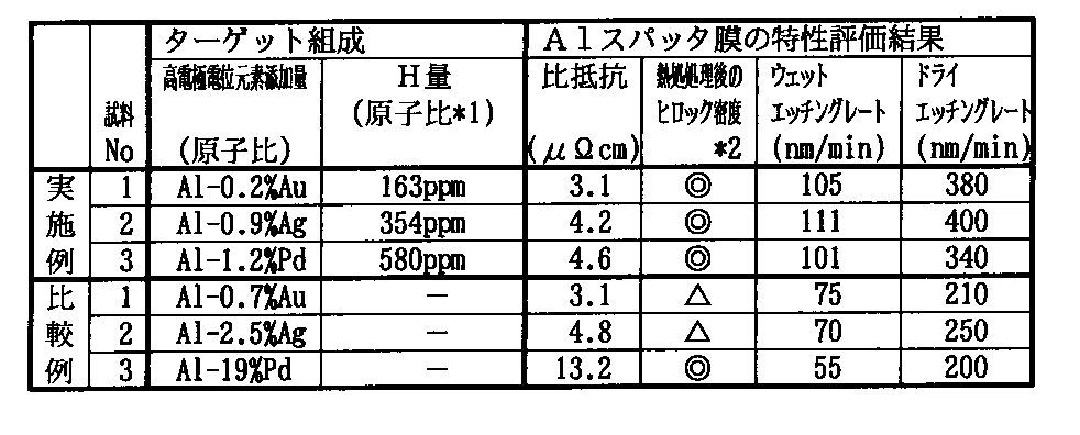
表1から明らかなように、本発明のAl配線膜は、耐ヒロック性およびエッチング性に優れることが分かる。よって、このようなAl配線膜を用いることによって、健全な微細配線網を再現性よく形成することが可能となる。 As is apparent from Table 1, the Al wiring film of the present invention is excellent in hillock resistance and etching property. Therefore, by using such an Al wiring film, a sound fine wiring network can be formed with good reproducibility.
実施例2
表2に示す各組成のAlスパッタターゲットを、それぞれ実施例1と同様にして作製した後、実施例1と同一条件でスパッタ成膜して、それぞれAl配線膜を得た。これら各Al配線膜の特性を実施例1と同様にして測定、評価した。その結果を併せて表2に示す。
Example 2
An Al sputter target having each composition shown in Table 2 was prepared in the same manner as in Example 1, and then sputtered under the same conditions as in Example 1 to obtain an Al wiring film. The characteristics of these Al wiring films were measured and evaluated in the same manner as in Example 1. The results are also shown in Table 2.
実施例3
Yに代えて各種元素を用いたAlターゲット(表3に組成を示す)を、それぞれ実施例1と同様にして作製した後、実施例1と同一条件でスパッタ成膜して、それぞれAl配線膜を得た。これら各Al配線膜の特性を実施例1と同様にして測定、評価した。また、試料No16〜21のAl配線膜については、アルカリ溶液中におけるITO電極との反応性も測定、評価した。このアルカリ溶液中におけるITO電極との反応性は、参照電極に銀・塩化銀電極を用いると共に、陽極をITO、陰極を各Al合金とし、通常用いられる電極測定法で調べた。その結果を併せて表3に示す。
Example 3
Al targets (compositions shown in Table 3) using various elements in place of Y were prepared in the same manner as in Example 1, and then sputtered under the same conditions as in Example 1 to obtain Al wiring films. Got. The characteristics of these Al wiring films were measured and evaluated in the same manner as in Example 1. Moreover, about the Al wiring film of sample No. 16-21, the reactivity with the ITO electrode in an alkaline solution was also measured and evaluated. The reactivity with the ITO electrode in this alkaline solution was investigated by a commonly used electrode measurement method using a silver / silver chloride electrode as a reference electrode, an ITO as an anode, and an Al alloy as a cathode. The results are also shown in Table 3.
実施例4
まず、Alに対して2.84原子%(6質量%)のCoを添加した原料を、高周波誘導溶解(真空溶解)し、この溶湯内にH2ガスをバブリングしてHを投入した。Hのバブリング量は、インゴット中のH量がCo量に対して980原子ppmとなるように設定した。このようにして作製した目的組成のインゴットに対して、熱間圧延および機械加工を施し、直径127mm×厚さ5mmのAlスパッタターゲットを得た。
Example 4
First, a raw material in which 2.84 atomic% (6% by mass) of Co was added to Al was induction-melted (vacuum melted), and H 2 gas was bubbled into the molten metal to introduce H. The amount of H bubbling was set so that the amount of H in the ingot was 980 atomic ppm relative to the amount of Co. The ingot having the target composition thus produced was hot-rolled and machined to obtain an Al sputter target having a diameter of 127 mm and a thickness of 5 mm.
このようにして得たAlスパッタターゲットを用いて、背圧1×10⁻⁴Pa、出力DC200W、スパッタ時間2minの条件で、直径5インチのガラス基板上に回転成膜して、厚さ350nmのAl膜を成膜した。このAl膜にパターニングおよびドライエッチングを施し、さらに573Kで熱処理を施した後、比抵抗、ヒロック密度、エッチング残渣の有無を測定評価した。これらの結果を表4に示す。なお、エッチング残渣の評価試験は、BCl3+Cl2の混合ガスをエッチングガスとして用いて行った。 Using the Al sputter target thus obtained, a film was rotated on a glass substrate having a diameter of 5 inches under the conditions of a back pressure of 1 × 10 −4 Pa, an output of DC 200 W, and a sputtering time of 2 min. An Al film was formed. This Al film was subjected to patterning and dry etching, and further subjected to heat treatment at 573 K, and then the specific resistance, hillock density, and the presence or absence of etching residue were measured and evaluated. These results are shown in Table 4. Note that the etching residue evaluation test was performed using a mixed gas of BCl 3 + Cl 2 as an etching gas.
また、本発明との比較例として、CoおよびHを添加しないで作製したAlスパッタターゲット(比較例4-1)と、Hを添加しない以外は実施例4と同一条件で作製したAlスパッタターゲット(比較例4-2)を用いて、それぞれ同様にAl膜をスパッタ成膜した。そして、これらAl膜についても実施例4と同様に特性を評価した。これらの結果を併せて表4に示す。 Moreover, as a comparative example with the present invention, an Al sputter target (Comparative Example 4-1) manufactured without adding Co and H, and an Al sputter target manufactured under the same conditions as Example 4 except that H is not added (Comparative Example 4-1) Using Comparative Example 4-2), an Al film was similarly formed by sputtering. The characteristics of these Al films were evaluated in the same manner as in Example 4. These results are shown together in Table 4.
表4から明らかなように、実施例4のAl配線膜は、耐ヒロック性およびエッチング性に優れることが分かる。よって、このようなAl配線膜を用いることによって、健全な微細配線網を再現性よく形成することが可能となる。 As can be seen from Table 4, the Al wiring film of Example 4 is excellent in hillock resistance and etching property. Therefore, by using such an Al wiring film, a sound fine wiring network can be formed with good reproducibility.
実施例5
表5に示す各組成のAlスパッタターゲットを、それぞれ実施例4と同様にして作製した後、実施例4と同一条件でスパッタ成膜した。このようにして作製した各Al膜をアルカリ溶液(NMD-3/現像液)中に入れ、参照電極(Ag/AgCl/Cl-)を用いて電極電位を測定した。その結果を表5および図8に示す。
Example 5
An Al sputter target having each composition shown in Table 5 was prepared in the same manner as in Example 4, and then sputtered under the same conditions as in Example 4. Each Al film thus produced was placed in an alkaline solution (NMD-3 / developer), and the electrode potential was measured using a reference electrode (Ag / AgCl / Cl − ). The results are shown in Table 5 and FIG.
表5および図8から明らかなように、Alより標準電極電位が高い元素を含有させたAl膜は、いずれもITOより電極電位が高いことが分かる。 As is apparent from Table 5 and FIG. 8, it can be seen that the Al film containing an element having a higher standard electrode potential than Al has a higher electrode potential than ITO.
実施例6
Alより標準電極電位が高い元素(Ir、Pt、V、Nb)を用いて、表6に組成を示すAlスパッタターゲットをそれぞれ実施例4と同様にして作製した後、実施例4と同一条件でスパッタ成膜して、それぞれAl配線膜を得た。これら各Al配線膜の特性を実施例1と同様にして測定、評価した。また、これらAl配線膜については、実施例3と同様にして、アルカリ溶液中におけるITO電極との反応性も測定、評価した。その結果を併せて表6に示す。なお、表6中の比較例6は、高電極電位元素の含有量を本発明の範囲外としたものである。
Example 6
Using elements having higher standard electrode potential than Al (Ir, Pt, V, Nb), Al sputter targets having the compositions shown in Table 6 were prepared in the same manner as in Example 4, and then under the same conditions as in Example 4. Sputter deposition was performed to obtain Al wiring films. The characteristics of these Al wiring films were measured and evaluated in the same manner as in Example 1. Moreover, about these Al wiring films, the reactivity with the ITO electrode in an alkaline solution was also measured and evaluated in the same manner as in Example 3. The results are also shown in Table 6. In Comparative Example 6 in Table 6, the content of the high electrode potential element is outside the scope of the present invention.
表6から明らかなように、高電極電位元素の含有量が多すぎると、比抵抗が増大すると共に、適量のHを含有させてもエッチング残渣を防止することができない。一方、高電極電位元素の含有量が少なすぎると、ヒロックの発生およびITO電極との反応を防止することができない。これらに対して、適量の高電極電位元素およびHを含有させた実施例6による各Al配線膜は、比抵抗、耐ヒロック性、エッチング性、ITO電極との反応防止性に優れることが分かる。よって、このようなAl配線膜を用いることによって、健全な微細配線網を再現性よく形成することが可能となる。また、LCDのゲート線等も健全に形成することができる。 As is clear from Table 6, if the content of the high electrode potential element is too large, the specific resistance increases, and even if an appropriate amount of H is contained, etching residues cannot be prevented. On the other hand, if the content of the high electrode potential element is too small, generation of hillocks and reaction with the ITO electrode cannot be prevented. On the other hand, it can be seen that each Al wiring film according to Example 6 containing an appropriate amount of high electrode potential element and H is excellent in specific resistance, hillock resistance, etching property, and resistance to reaction with the ITO electrode. Therefore, by using such an Al wiring film, a sound fine wiring network can be formed with good reproducibility. Also, the gate lines of the LCD can be formed soundly.
実施例7
Alより標準電極電位が高い元素(Au、Ag、Pd)を用いて、表7に組成を示すAlスパッタターゲットをそれぞれ実施例4と同様にして作製した後、実施例4と同一条件でスパッタ成膜して、それぞれAl配線膜を得た。これら各Al配線膜の特性を実施例1と同様にして測定、評価した。また、Al配線膜のエッチング性については、ウェットエッチングおよびドライエッチングそれぞれのエッチングレートを調べた。その結果を表7に示す。なお、表7中の比較例7は、Hを添加しない以外は実施例7と同一条件で作製したAlスパッタターゲットを用いて、それぞれ同様にスパッタ成膜したAl膜である。
Example 7
Using elements (Au, Ag, Pd) having a higher standard electrode potential than Al, Al sputtering targets having the compositions shown in Table 7 were prepared in the same manner as in Example 4, and then sputtered under the same conditions as in Example 4. The Al wiring films were obtained. The characteristics of these Al wiring films were measured and evaluated in the same manner as in Example 1. As for the etching properties of the Al wiring film, the etching rates of wet etching and dry etching were examined. The results are shown in Table 7. In addition, Comparative Example 7 in Table 7 is an Al film formed by sputtering in the same manner using an Al sputter target manufactured under the same conditions as in Example 7 except that H is not added.
表7から明らかなように、適量の高電極電位元素およびHを含有させた実施例7による各Al配線膜は、比抵抗および耐ヒロック性に優れ、さらにエッチングレート性も高いことが分かる。よって、このようなAl配線膜を用いることによって、健全な微細配線網を再現性よくかつ効率よく形成することができる。 As can be seen from Table 7, each Al wiring film according to Example 7 containing an appropriate amount of high electrode potential element and H is excellent in specific resistance and hillock resistance, and also has a high etching rate. Therefore, by using such an Al wiring film, a healthy fine wiring network can be formed with good reproducibility and efficiency.
実施例8
表8に組成を示すAlスパッタターゲットを、それぞれ実施例4と同様にして作製した後、実施例4と同一条件でスパッタ成膜して、それぞれAl配線膜を得た。これら各Al配線膜の特性を実施例1と同様にして測定、評価した。その結果を表8に示す。
Example 8
Al sputter targets having the compositions shown in Table 8 were prepared in the same manner as in Example 4, and then sputtered under the same conditions as in Example 4 to obtain Al wiring films. The characteristics of these Al wiring films were measured and evaluated in the same manner as in Example 1. The results are shown in Table 8.
実施例9
まず、Alに対して0.3原子%(2質量%)のTaを添加した原料を、高周波誘導溶解(真空溶解)し、溶解時にO2をバブリングして酸素を投入した。酸素の投入量は、インゴット中のO量がTa量に対して10原子ppmとなるように設定した。このようにして作製した目的組成のインゴットに対して、熱間圧延および機械加工を施し、直径127mm×厚さ5mmのAlスパッタターゲットを得た。
Example 9
First, high-frequency induction melting (vacuum melting) was performed on a raw material in which 0.3 atomic% (2% by mass) of Ta was added to Al, and O 2 was bubbled at the time of melting to introduce oxygen. The amount of oxygen input was set so that the amount of O in the ingot was 10 atomic ppm relative to the amount of Ta. The ingot having the target composition thus produced was hot-rolled and machined to obtain an Al sputter target having a diameter of 127 mm and a thickness of 5 mm.
このようにして得たAlスパッタターゲットを用いて、背圧1×10⁻⁴Pa、出力DC200W、スパッタ時間2minの条件で、直径5インチのガラス基板上に回転成膜して、厚さ350nmのAl膜を成膜した。このAl膜にパターニングおよびドライエッチングを施し、さらに573Kで熱処理を施した後、比抵抗、ヒロック密度、エッチング残渣の有無を測定評価した。これらの結果を表9に示す。なお、エッチング残渣の評価試験は、BCl3+Cl2の混合ガスをエッチングガスとして用いて行った。 Using the Al sputter target thus obtained, a film was rotated on a glass substrate having a diameter of 5 inches under the conditions of a back pressure of 1 × 10 −4 Pa, an output of DC 200 W, and a sputtering time of 2 min. An Al film was formed. This Al film was subjected to patterning and dry etching, and further subjected to heat treatment at 573 K, and then the specific resistance, hillock density, and the presence or absence of etching residue were measured and evaluated. These results are shown in Table 9. Note that the etching residue evaluation test was performed using a mixed gas of BCl 3 + Cl 2 as an etching gas.
また、本発明との比較例として、TaおよびOを添加しないで作製したAlスパッタターゲット(比較例9-1)と、Oを添加しない以外は実施例9と同一条件で作製したAlスパッタターゲット(比較例9-2)を用いて、それぞれ同様にAl膜をスパッタ成膜した。そして、これらAl膜についても実施例9と同様に特性を評価した。これらの結果を併せて表9に示す。 Moreover, as a comparative example with the present invention, an Al sputter target (Comparative Example 9-1) produced without adding Ta and O and an Al sputter target produced under the same conditions as Example 9 except that O is not added (Comparative Example 9-1) Using Comparative Example 9-2), an Al film was similarly formed by sputtering. The characteristics of these Al films were evaluated in the same manner as in Example 9. These results are shown together in Table 9.
表9から明らかなように、実施例9のAl配線膜は、耐ヒロック性およびエッチング性に優れることが分かる。よって、このようなAl配線膜を用いることによって、健全な微細配線網を再現性よく形成することが可能となる。 As is apparent from Table 9, it can be seen that the Al wiring film of Example 9 is excellent in hillock resistance and etching property. Therefore, by using such an Al wiring film, a sound fine wiring network can be formed with good reproducibility.
実施例10
各種元素を用いたAlターゲット(表10に組成を示す)を、それぞれ実施例9と同様にして作製した後、実施例9と同一条件でスパッタ成膜して、それぞれAl配線膜を得た。これら各Al配線膜の特性を実施例1と同様にして測定、評価した。また、試料No5〜6のAl配線膜については、実施例3と同様にして、アルカリ溶液中におけるITO電極との反応性も測定、評価した。その結果を表10に示す。なお、表10中の比較例10は、添加元素量を本発明の範囲外としたものである。
Example 10
After preparing Al targets (compositions shown in Table 10) using various elements in the same manner as in Example 9, sputtering was performed under the same conditions as in Example 9 to obtain Al wiring films, respectively. The characteristics of these Al wiring films were measured and evaluated in the same manner as in Example 1. For the Al wiring films of Samples Nos. 5 to 6, the reactivity with the ITO electrode in the alkaline solution was also measured and evaluated in the same manner as in Example 3. The results are shown in Table 10. In addition, the comparative example 10 in Table 10 makes the amount of additive elements outside the scope of the present invention.
実施例11
まず、Alに対して0.28原子%(2質量%)のPtを添加した原料を、高周波誘導溶解(真空溶解)し、溶解時にN2をバブリングして窒素を投入した。窒素の投入量は、インゴット中のN量がPt量に対して19原子ppmとなるように設定した。このようにして作製した目的組成のインゴットに対して、熱間圧延および機械加工を施し、直径127mm×厚さ5mmのAlスパッタターゲットを得た。
Example 11
First, a raw material in which 0.28 atomic% (2% by mass) of Pt was added to Al was induction-melted (vacuum melted), and N 2 was bubbled at the time of melting to introduce nitrogen. The input amount of nitrogen was set so that the N amount in the ingot was 19 atomic ppm with respect to the Pt amount. The ingot having the target composition thus produced was hot-rolled and machined to obtain an Al sputter target having a diameter of 127 mm and a thickness of 5 mm.
このようにして得たAlスパッタターゲットを用いて、背圧1×10⁻⁴Pa、出力DC200W、スパッタ時間2minの条件で、直径5インチのガラス基板上に回転成膜して、厚さ350nmのAl膜を成膜した。このAl膜にパターニングおよびドライエッチングを施し、さらに573Kで熱処理を施した後、比抵抗、ヒロック密度、エッチング残渣の有無を測定評価した。これらの結果を表11に示す。なお、エッチング残渣の評価試験は、BCl3+Cl2の混合ガスをエッチングガスとして用いて行った。 Using the Al sputter target thus obtained, a film was rotated on a glass substrate having a diameter of 5 inches under the conditions of a back pressure of 1 × 10 −4 Pa, an output of DC 200 W, and a sputtering time of 2 min. An Al film was formed. This Al film was subjected to patterning and dry etching, and further subjected to heat treatment at 573 K, and then the specific resistance, hillock density, and the presence or absence of etching residue were measured and evaluated. These results are shown in Table 11. Note that the etching residue evaluation test was performed using a mixed gas of BCl 3 + Cl 2 as an etching gas.
また、本発明との比較例として、PtおよびNを添加しないで作製したAlスパッタターゲット(比較例11-1)と、Nを添加しない以外は実施例11と同一条件で作製したAlスパッタターゲット(比較例11-2)を用いて、それぞれ同様にAl膜をスパッタ成膜した。そして、これらAl膜についても実施例11と同様に特性を評価した。これらの結果を併せて表11に示す。 Further, as a comparative example with the present invention, an Al sputter target (Comparative Example 11-1) manufactured without adding Pt and N and an Al sputter target manufactured under the same conditions as in Example 11 except that N is not added (Comparative Example 11-1). Using Comparative Example 11-2), an Al film was similarly formed by sputtering. The characteristics of these Al films were evaluated in the same manner as in Example 11. These results are shown together in Table 11.
表11から明らかなように、実施例11のAl配線膜は、耐ヒロック性およびエッチング性に優れることが分かる。よって、このようなAl配線膜を用いることによって、健全な微細配線網を再現性よく形成することが可能となる。 As apparent from Table 11, the Al wiring film of Example 11 is excellent in hillock resistance and etching property. Therefore, by using such an Al wiring film, a sound fine wiring network can be formed with good reproducibility.
実施例12
各種元素を用いたAlターゲット(表12に組成を示す)を、それぞれ実施例11と同様にして作製した後、実施例11と同一条件でスパッタ成膜して、それぞれAl配線膜を得た。これら各Al配線膜の特性を実施例1と同様にして測定、評価した。なお、表12中の比較例12は、添加元素量を本発明の範囲外としたものである。
Example 12
After preparing Al targets (compositions shown in Table 12) using various elements in the same manner as in Example 11, sputtering was performed under the same conditions as in Example 11 to obtain Al wiring films. The characteristics of these Al wiring films were measured and evaluated in the same manner as in Example 1. In addition, the comparative example 12 in Table 12 makes the amount of added elements out of the scope of the present invention.
2′…Al配線膜からなるゲート電極、29…Al配線、35…Al配線膜からなる個別電極、36…Al配線膜からなる共通電極、42、43…Al配線膜からなるトランスジューサ。 2 '... gate electrode made of Al wiring film, 29 ... Al wiring, 35 ... individual electrode made of Al wiring film, 36 ... common electrode made of Al wiring film, 42, 43 ... transducer made of Al wiring film.
Claims (6)
前記インゴットまたは焼結体を加工してスパッタターゲットを作製する工程と
を具備することを特徴とするスパッタターゲットの製造方法。 Y, Sc, La, Ce, Nd, Sm, Gd, Tb, Dy, Er, Th, Sr, Ti, Zr, V, Nb, Ta, Cr, Mo, W, Mn, Tc, Re, Fe, Co, It contains at least one first element selected from Ni, Pd, Ir, Pt, Cu, Ag, Au, Cd, Si, Pb and B in a range of 0.001 to 30 atomic%, and the balance is substantially made of Al. A gas containing at least one second element selected from O, N, and H is used in producing the ingot or sintered body by the atmospheric melting method, the vacuum melting method, the rapid solidification method, or the powder metallurgy method. And producing the ingot or sintered body,
And a step of manufacturing the sputter target by processing the ingot or the sintered body.
前記インゴットまたは焼結体の作製工程に前記大気溶解法または真空溶解法を適用し、かつ溶解中に前記第2の元素を含むガスでバブリングすることを特徴とするスパッタターゲットの製造方法。 In the manufacturing method of the sputter target according to claim 1,
A sputtering target manufacturing method, wherein the atmospheric melting method or the vacuum melting method is applied to a manufacturing process of the ingot or sintered body, and bubbling is performed with a gas containing the second element during the melting.
前記インゴットまたは焼結体の作製工程に前記急冷凝固法としてスプレーフォーミング法を適用し、かつスプレー時に前記第2の元素を含むガスを吹き付けることを特徴とするスパッタターゲットの製造方法。 In the manufacturing method of the sputter target according to claim 1,
A method of manufacturing a sputter target, wherein a spray forming method is applied as the rapid solidification method to the ingot or sintered body manufacturing step, and a gas containing the second element is sprayed during spraying.
前記インゴットまたは焼結体に前記第2の元素を前記第1の元素量に対して0.01原子ppm〜50原子%の範囲で含有させることを特徴とするスパッタターゲットの製造方法。 In the manufacturing method of the sputter target according to any one of claims 1 to 3,
A method for producing a sputter target, wherein the ingot or sintered body contains the second element in a range of 0.01 atomic ppm to 50 atomic% with respect to the amount of the first element.
前記インゴットまたは焼結体に前記第2の元素を前記第1の元素量に対して0.01原子ppm〜7.5原子%の範囲で含有させることを特徴とするスパッタターゲットの製造方法。 In the manufacturing method of the sputter target according to any one of claims 1 to 3,
A method for producing a sputter target, wherein the ingot or sintered body contains the second element in a range of 0.01 atomic ppm to 7.5 atomic% with respect to the amount of the first element.
前記第1の元素はAlと金属間化合物を形成する元素であることを特徴とするスパッタターゲットの製造方法。 In the manufacturing method of the sputter target according to any one of claims 1 to 5,
The method of manufacturing a sputter target, wherein the first element is an element that forms an intermetallic compound with Al.
Priority Applications (1)
| Application Number | Priority Date | Filing Date | Title |
|---|---|---|---|
| JP2005276818A JP4488991B2 (en) | 1995-10-12 | 2005-09-22 | Manufacturing method of sputter target |
Applications Claiming Priority (2)
| Application Number | Priority Date | Filing Date | Title |
|---|---|---|---|
| JP26447295 | 1995-10-12 | ||
| JP2005276818A JP4488991B2 (en) | 1995-10-12 | 2005-09-22 | Manufacturing method of sputter target |
Related Parent Applications (1)
| Application Number | Title | Priority Date | Filing Date |
|---|---|---|---|
| JP51492097A Division JP4137182B2 (en) | 1995-10-12 | 1996-10-14 | Sputter target for wiring film formation |
Related Child Applications (1)
| Application Number | Title | Priority Date | Filing Date |
|---|---|---|---|
| JP2009069802A Division JP5175780B2 (en) | 1995-10-12 | 2009-03-23 | Manufacturing method of sputter target |
Publications (2)
| Publication Number | Publication Date |
|---|---|
| JP2006111969A true JP2006111969A (en) | 2006-04-27 |
| JP4488991B2 JP4488991B2 (en) | 2010-06-23 |
Family
ID=17403704
Family Applications (7)
| Application Number | Title | Priority Date | Filing Date |
|---|---|---|---|
| JP51492097A Expired - Lifetime JP4137182B2 (en) | 1995-10-12 | 1996-10-14 | Sputter target for wiring film formation |
| JP2004076172A Expired - Lifetime JP4130418B2 (en) | 1995-10-12 | 2004-03-17 | Wiring film, manufacturing method thereof, and electronic component using the same |
| JP2005276818A Expired - Lifetime JP4488991B2 (en) | 1995-10-12 | 2005-09-22 | Manufacturing method of sputter target |
| JP2005276820A Expired - Fee Related JP4589854B2 (en) | 1995-10-12 | 2005-09-22 | Manufacturing method of Al alloy wiring |
| JP2005276819A Expired - Lifetime JP4488992B2 (en) | 1995-10-12 | 2005-09-22 | Manufacturing method of sputter target |
| JP2009069802A Expired - Lifetime JP5175780B2 (en) | 1995-10-12 | 2009-03-23 | Manufacturing method of sputter target |
| JP2009245733A Expired - Lifetime JP5175824B2 (en) | 1995-10-12 | 2009-10-26 | Manufacturing method of sputter target |
Family Applications Before (2)
| Application Number | Title | Priority Date | Filing Date |
|---|---|---|---|
| JP51492097A Expired - Lifetime JP4137182B2 (en) | 1995-10-12 | 1996-10-14 | Sputter target for wiring film formation |
| JP2004076172A Expired - Lifetime JP4130418B2 (en) | 1995-10-12 | 2004-03-17 | Wiring film, manufacturing method thereof, and electronic component using the same |
Family Applications After (4)
| Application Number | Title | Priority Date | Filing Date |
|---|---|---|---|
| JP2005276820A Expired - Fee Related JP4589854B2 (en) | 1995-10-12 | 2005-09-22 | Manufacturing method of Al alloy wiring |
| JP2005276819A Expired - Lifetime JP4488992B2 (en) | 1995-10-12 | 2005-09-22 | Manufacturing method of sputter target |
| JP2009069802A Expired - Lifetime JP5175780B2 (en) | 1995-10-12 | 2009-03-23 | Manufacturing method of sputter target |
| JP2009245733A Expired - Lifetime JP5175824B2 (en) | 1995-10-12 | 2009-10-26 | Manufacturing method of sputter target |
Country Status (6)
| Country | Link |
|---|---|
| US (2) | US6329275B1 (en) |
| EP (2) | EP1553205B1 (en) |
| JP (7) | JP4137182B2 (en) |
| KR (1) | KR100312548B1 (en) |
| TW (1) | TW318276B (en) |
| WO (1) | WO1997013885A1 (en) |
Cited By (6)
| Publication number | Priority date | Publication date | Assignee | Title |
|---|---|---|---|---|
| EP1746173A2 (en) * | 2005-07-22 | 2007-01-24 | Heraeus, Inc. | Enhanced sputter target manufacturing method |
| EP1923481A2 (en) * | 2005-07-22 | 2008-05-21 | Heraeus, Inc. | Enhanced sputter target manufacturing method |
| USRE41975E1 (en) | 1995-10-12 | 2010-11-30 | Kabushiki Kaisha Toshiba | Interconnector line of thin film, sputter target for forming the wiring film and electronic component using the same |
| USRE45481E1 (en) | 1995-10-12 | 2015-04-21 | Kabushiki Kaisha Toshiba | Interconnector line of thin film, sputter target for forming the wiring film and electronic component using the same |
| JP2015096647A (en) * | 2013-10-08 | 2015-05-21 | 株式会社フルヤ金属 | Alloy target of aluminum and rare earth element and manufacturing method of the same |
| KR20210011455A (en) * | 2018-06-28 | 2021-02-01 | 가부시키가이샤 아루박 | Aluminum alloy target and its manufacturing method |
Families Citing this family (78)
| Publication number | Priority date | Publication date | Assignee | Title |
|---|---|---|---|---|
| JPH10142625A (en) * | 1996-11-07 | 1998-05-29 | Vacuum Metallurgical Co Ltd | Manufacture of liquid crystal display conductive part, and sputtering target used for manufacture thereof |
| TW574394B (en) * | 1997-07-15 | 2004-02-01 | Micron Technology Inc | Method of using hydrogen and oxygen gas in sputter deposition of aluminum-containing films and aluminum-containing films derived therefrom |
| US6222271B1 (en) | 1997-07-15 | 2001-04-24 | Micron Technology, Inc. | Method of using hydrogen gas in sputter deposition of aluminum-containing films and aluminum-containing films derived therefrom |
| US5969423A (en) | 1997-07-15 | 1999-10-19 | Micron Technology, Inc. | Aluminum-containing films derived from using hydrogen and oxygen gas in sputter deposition |
| US6448708B1 (en) | 1997-09-17 | 2002-09-10 | Candescent Intellectual Property Services, Inc. | Dual-layer metal for flat panel display |
| JP4197579B2 (en) * | 1997-12-24 | 2008-12-17 | 株式会社東芝 | Sputtering target, Al wiring film manufacturing method using the same, and electronic component manufacturing method |
| US6710525B1 (en) | 1999-10-19 | 2004-03-23 | Candescent Technologies Corporation | Electrode structure and method for forming electrode structure for a flat panel display |
| ATE441737T1 (en) * | 2000-12-28 | 2009-09-15 | Kobe Steel Ltd | TARGET FOR FORMING A HARD LAYER |
| JP2002373867A (en) * | 2001-06-14 | 2002-12-26 | Idemitsu Kosan Co Ltd | Semiconductor device, electrically conductive thin film therefor, and method of manufacturing the same |
| JP2003089864A (en) * | 2001-09-18 | 2003-03-28 | Mitsui Mining & Smelting Co Ltd | Aluminum alloy thin film, wiring circuit having the same thin film, and target material depositing the thin film |
| EP1474829A1 (en) * | 2002-01-24 | 2004-11-10 | Honeywell International, Inc. | Thin films, structures having thin films, and methods of forming thin films |
| JP2004143584A (en) * | 2002-08-29 | 2004-05-20 | Nippon Sheet Glass Co Ltd | Article coated with zirconium compound film, method for producing the article, and sputtering target used for coating with the film |
| EP1411146B1 (en) * | 2002-10-17 | 2010-06-09 | Samsung Electronics Co., Ltd. | Method of forming cobalt silicide film and method of manufacturing semiconductor device having cobalt silicide film |
| JP2006339666A (en) * | 2002-12-19 | 2006-12-14 | Kobe Steel Ltd | Sputtering target for forming aluminum-alloy film |
| JP3940385B2 (en) * | 2002-12-19 | 2007-07-04 | 株式会社神戸製鋼所 | Display device and manufacturing method thereof |
| CN1307694C (en) * | 2003-06-03 | 2007-03-28 | 旺宏电子股份有限公司 | Method for lowering resistance value of cobalt disilicide layer of semiconductor devices |
| US7030430B2 (en) * | 2003-08-15 | 2006-04-18 | Intel Corporation | Transition metal alloys for use as a gate electrode and devices incorporating these alloys |
| JP2005086118A (en) * | 2003-09-11 | 2005-03-31 | Renesas Technology Corp | Semiconductor device |
| KR100762815B1 (en) * | 2003-12-18 | 2007-10-02 | 미쓰이 긴조꾸 고교 가부시키가이샤 | Aluminum base target |
| US8004173B2 (en) * | 2004-01-22 | 2011-08-23 | Canon Kabushiki Kaisha | Antistatic film, spacer using it and picture display unit |
| KR101101456B1 (en) * | 2004-03-09 | 2012-01-03 | 이데미쓰 고산 가부시키가이샤 | Thin-film transistor and thin-film transistor substrate and production methods for them and liquid crystal display unit using these and related device and method, and, sputtering target and transparent conductive film formed by using this and transparent electrode and related device and method |
| CN100417993C (en) * | 2004-03-25 | 2008-09-10 | 三井金属鉱业株式会社 | Bonding structure of thin film circuit |
| JP4646912B2 (en) * | 2004-03-25 | 2011-03-09 | 三井金属鉱業株式会社 | Thin film circuit junction structure |
| JP4849821B2 (en) * | 2004-04-28 | 2012-01-11 | 株式会社半導体エネルギー研究所 | Display device, electronic equipment |
| US7550769B2 (en) | 2004-06-11 | 2009-06-23 | Semiconductor Energy Laboratory Co., Ltd. | Light emitting element, light emitting device and semiconductor device |
| JP5060714B2 (en) * | 2004-09-30 | 2012-10-31 | 株式会社神戸製鋼所 | Hard coating excellent in wear resistance and oxidation resistance, and target for forming the hard coating |
| WO2006057312A1 (en) * | 2004-11-24 | 2006-06-01 | Tosoh Corporation | Wiring/electrode and sputtering target |
| WO2006117884A1 (en) * | 2005-04-26 | 2006-11-09 | Mitsui Mining & Smelting Co., Ltd. | Al-Ni-B ALLOY WIRING MATERIAL AND DEVICE STRUCTURE USING SAME |
| WO2006117954A1 (en) * | 2005-04-26 | 2006-11-09 | Mitsui Mining & Smelting Co., Ltd. | Al-Ni-B ALLOY WIRING MATERIAL AND ELEMENT STRUCTURE USING THE SAME |
| JP4117002B2 (en) | 2005-12-02 | 2008-07-09 | 株式会社神戸製鋼所 | Thin film transistor substrate and display device |
| JP2007191761A (en) * | 2006-01-19 | 2007-08-02 | Idemitsu Kosan Co Ltd | Stacked structure, electrode for electric circuit using the same and method for producing the same |
| KR20080100358A (en) * | 2006-03-06 | 2008-11-17 | 토소우 에스엠디, 인크 | Electronic device, method of manufacture of same and sputtering target |
| CN101395296B (en) * | 2006-03-06 | 2012-03-28 | 陶斯摩有限公司 | Sputtering target |
| JP4728170B2 (en) * | 2006-05-26 | 2011-07-20 | 三菱電機株式会社 | Semiconductor device and active matrix display device |
| JP5234892B2 (en) * | 2006-05-31 | 2013-07-10 | 株式会社神戸製鋼所 | Thin film transistor substrate and display device |
| CN101365816B (en) | 2006-10-16 | 2010-10-06 | 三井金属鉱业株式会社 | Al-Ni-B alloy material for reflection film |
| KR101010949B1 (en) | 2006-10-26 | 2011-01-26 | 미쓰이 긴조꾸 고교 가부시키가이샤 | Element structure of display device and manufacturing method of the same |
| JP4377906B2 (en) * | 2006-11-20 | 2009-12-02 | 株式会社コベルコ科研 | Al-Ni-La-based Al-based alloy sputtering target and method for producing the same |
| WO2008066030A1 (en) * | 2006-11-30 | 2008-06-05 | Kabushiki Kaisha Kobe Seiko Sho | Al ALLOY FILM FOR DISPLAY DEVICE, DISPLAY DEVICE, AND SPUTTERING TARGET |
| JP4170367B2 (en) * | 2006-11-30 | 2008-10-22 | 株式会社神戸製鋼所 | Al alloy film for display device, display device, and sputtering target |
| KR100818525B1 (en) * | 2006-12-20 | 2008-03-31 | 동부일렉트로닉스 주식회사 | Image senser and method mamufacturing of the same |
| KR100853545B1 (en) | 2007-05-15 | 2008-08-21 | 삼성에스디아이 주식회사 | Organic light emitting display device and fabrication method of the same |
| JP2009010052A (en) * | 2007-06-26 | 2009-01-15 | Kobe Steel Ltd | Method of manufacturing display device |
| JP2009008770A (en) | 2007-06-26 | 2009-01-15 | Kobe Steel Ltd | Laminated structure and method for manufacturing the same |
| JP5143649B2 (en) * | 2007-07-24 | 2013-02-13 | 株式会社コベルコ科研 | Al-Ni-La-Si-based Al alloy sputtering target and method for producing the same |
| JP2009076536A (en) | 2007-09-19 | 2009-04-09 | Mitsubishi Electric Corp | Aluminum alloy film, electronic device, and active matrix substrate for electro-optical display device |
| CN101918888B (en) * | 2008-03-31 | 2013-07-31 | 株式会社神户制钢所 | Display device, process for producing the display device, and sputtering target |
| JP5308760B2 (en) * | 2008-09-30 | 2013-10-09 | 株式会社日立製作所 | Display device |
| CN102473644A (en) * | 2009-07-31 | 2012-05-23 | 国立大学法人东北大学 | Semiconductor device, method for manufacturing semiconductor device, and display device |
| WO2011058882A1 (en) | 2009-11-13 | 2011-05-19 | Semiconductor Energy Laboratory Co., Ltd. | Sputtering target and manufacturing method thereof, and transistor |
| WO2011058867A1 (en) * | 2009-11-13 | 2011-05-19 | Semiconductor Energy Laboratory Co., Ltd. | Sputtering target and method for manufacturing the same, and transistor |
| CN104795323B (en) * | 2009-12-04 | 2017-12-29 | 株式会社半导体能源研究所 | Semiconductor device and its manufacture method |
| TW201140627A (en) * | 2010-05-05 | 2011-11-16 | Univ Nat Yunlin Sci & Tech | Method for producing aluminum foil electrode of carbon nano-tube |
| JP5032687B2 (en) * | 2010-09-30 | 2012-09-26 | 株式会社神戸製鋼所 | Al alloy film, wiring structure having Al alloy film, and sputtering target used for production of Al alloy film |
| US8894825B2 (en) | 2010-12-17 | 2014-11-25 | Semiconductor Energy Laboratory Co., Ltd. | Sputtering target, method for manufacturing the same, manufacturing semiconductor device |
| JP5909852B2 (en) * | 2011-02-23 | 2016-04-27 | ソニー株式会社 | Manufacturing method of semiconductor device |
| JP2012186199A (en) * | 2011-03-03 | 2012-09-27 | Toshiba Corp | Semiconductor light-emitting device and method of manufacturing the same |
| CN103952604B (en) * | 2014-04-10 | 2016-06-08 | 安徽银力铸造有限公司 | A kind of automobile rust-preventing aluminum alloy |
| CN104451281A (en) * | 2014-12-25 | 2015-03-25 | 春焱电子科技(苏州)有限公司 | Aluminum alloy for electronic material |
| US10494712B2 (en) * | 2015-05-21 | 2019-12-03 | Jx Nippon Mining & Metals Corporation | Copper alloy sputtering target and method for manufacturing same |
| EP3184669B1 (en) * | 2015-12-23 | 2018-07-18 | ATOTECH Deutschland GmbH | Etching solution for copper and copper alloy surfaces |
| JP6574714B2 (en) * | 2016-01-25 | 2019-09-11 | 株式会社コベルコ科研 | Wiring structure and sputtering target |
| CN105586576A (en) * | 2016-02-04 | 2016-05-18 | 东莞沙头朝日五金电子制品有限公司 | Method for plating physical vapor deposition (PVD) anti-microbial film |
| CN109312449B (en) * | 2016-06-07 | 2022-04-12 | Jx金属株式会社 | Sputtering target and method for producing same |
| CN106555083B (en) * | 2016-12-05 | 2018-03-20 | 合肥工业大学 | A kind of all aluminium alloy aerial condutor and preparation method thereof |
| CN106521250B (en) * | 2016-12-05 | 2018-03-20 | 合肥工业大学 | A kind of preparation method of big current-carrying heat-resistant aluminum alloy wire |
| SG11201908429SA (en) * | 2017-03-13 | 2019-10-30 | Materion Corp | Aluminum-scandium alloys with high uniformity and elemental content and articles thereof |
| US10760156B2 (en) | 2017-10-13 | 2020-09-01 | Honeywell International Inc. | Copper manganese sputtering target |
| US11035036B2 (en) | 2018-02-01 | 2021-06-15 | Honeywell International Inc. | Method of forming copper alloy sputtering targets with refined shape and microstructure |
| CN108396205B (en) * | 2018-04-28 | 2020-09-04 | 广州致远新材料科技有限公司 | Aluminum alloy material and preparation method thereof |
| US11935936B2 (en) | 2018-06-28 | 2024-03-19 | Ulvac, Inc. | Aluminum alloy film, method of producing the same, and thin film transistor |
| KR20220018548A (en) * | 2019-07-31 | 2022-02-15 | 가부시키가이샤 후루야긴조쿠 | sputtering target |
| JP7096291B2 (en) * | 2019-11-26 | 2022-07-05 | 株式会社フルヤ金属 | Sputtering target |
| CN110923529A (en) * | 2019-11-29 | 2020-03-27 | 安徽峰创云通数据科技有限公司 | Al-Cu-Sr-RE-Ge aluminum alloy wire for power cable and preparation method thereof |
| KR102329427B1 (en) * | 2020-01-03 | 2021-11-24 | 와이엠씨 주식회사 | Alloy composition for wired electrodes and manufacturing method thereof |
| KR102329426B1 (en) * | 2020-01-03 | 2021-11-24 | 와이엠씨 주식회사 | Alloy composition for wired electrodes and manufacturing method thereof |
| JP7133727B2 (en) * | 2020-06-30 | 2022-09-08 | 株式会社アルバック | Metal wiring structure and method for manufacturing metal wiring structure |
| WO2023189074A1 (en) * | 2022-03-29 | 2023-10-05 | 株式会社村田製作所 | Elastic wave device |
Family Cites Families (25)
| Publication number | Priority date | Publication date | Assignee | Title |
|---|---|---|---|---|
| US4302498A (en) * | 1980-10-28 | 1981-11-24 | Rca Corporation | Laminated conducting film on an integrated circuit substrate and method of forming the laminate |
| JPS62228446A (en) | 1985-11-29 | 1987-10-07 | Nippon Mining Co Ltd | Aluminum alloy for semiconductor wiring material |
| JPH0656883B2 (en) | 1986-03-03 | 1994-07-27 | 鐘淵化学工業株式会社 | Semiconductor device |
| JPS62235454A (en) * | 1986-04-03 | 1987-10-15 | Nippon Mining Co Ltd | N-containing al alloy for semiconductor wiring material |
| JPS62240738A (en) | 1986-04-11 | 1987-10-21 | Nippon Mining Co Ltd | N-and c-containing aluminum alloy for semiconductor wiring material |
| JPH0768612B2 (en) | 1987-04-20 | 1995-07-26 | 日立金属株式会社 | Alloy powder for rare earth metal-iron group metal target, rare earth metal-iron group metal target, and methods for producing the same |
| JPS6425977U (en) | 1987-08-07 | 1989-02-14 | ||
| JPS6457965A (en) * | 1987-08-27 | 1989-03-06 | Sumitomo Electric Industries | Production of spiral part by spray forming of aluminum alloy |
| JPH0649933B2 (en) * | 1987-09-18 | 1994-06-29 | 日本鋼管株式会社 | Plated steel plate for cans |
| JPH01134426A (en) | 1987-11-20 | 1989-05-26 | Hitachi Ltd | Thin film transistor for driving liquid crystal display |
| JP2597380B2 (en) | 1988-03-23 | 1997-04-02 | 日立金属株式会社 | Method for producing rare earth metal-transition metal target alloy powder and method for producing rare earth metal-transition metal target |
| JP2714606B2 (en) | 1988-05-16 | 1998-02-16 | 日本電信電話株式会社 | Wiring layer and its manufacturing method |
| DE3911657A1 (en) | 1989-04-10 | 1990-10-11 | Telefunken Electronic Gmbh | Semiconductor component with metallising on basic body - consists of four different materials for switching active semiconductor regions |
| US5367179A (en) * | 1990-04-25 | 1994-11-22 | Casio Computer Co., Ltd. | Thin-film transistor having electrodes made of aluminum, and an active matrix panel using same |
| JP3282204B2 (en) | 1991-12-24 | 2002-05-13 | カシオ計算機株式会社 | Method of forming aluminum-based alloy film |
| JPH0441063A (en) * | 1990-06-06 | 1992-02-12 | Nkk Corp | Spray forming method |
| JPH0448854A (en) | 1990-06-15 | 1992-02-18 | Sharp Corp | Data communication equipment system |
| JP3061654B2 (en) | 1991-04-23 | 2000-07-10 | 株式会社神戸製鋼所 | Semiconductor device material for liquid crystal display and molten sputtering target material for manufacturing semiconductor device material for liquid crystal display |
| JP3021996B2 (en) | 1991-09-30 | 2000-03-15 | 松下電器産業株式会社 | Aluminum wiring and method of forming the same |
| US5211824A (en) * | 1991-10-31 | 1993-05-18 | Siemens Solar Industries L.P. | Method and apparatus for sputtering of a liquid |
| DE69224038T2 (en) | 1991-11-15 | 1998-04-23 | Casio Computer Co Ltd | Thin film assembly with a conductive tie layer |
| JPH05239635A (en) | 1992-02-26 | 1993-09-17 | Shimadzu Corp | Production of transparent conductive film |
| JP2733006B2 (en) | 1993-07-27 | 1998-03-30 | 株式会社神戸製鋼所 | Electrode for semiconductor, method for manufacturing the same, and sputtering target for forming electrode film for semiconductor |
| JPH07246452A (en) * | 1994-03-09 | 1995-09-26 | Kobe Steel Ltd | Atomizing forming method |
| JP4137182B2 (en) | 1995-10-12 | 2008-08-20 | 株式会社東芝 | Sputter target for wiring film formation |
-
1996
- 1996-10-14 JP JP51492097A patent/JP4137182B2/en not_active Expired - Lifetime
- 1996-10-14 US US09/051,567 patent/US6329275B1/en not_active Ceased
- 1996-10-14 EP EP05003598.9A patent/EP1553205B1/en not_active Expired - Lifetime
- 1996-10-14 KR KR1019980702718A patent/KR100312548B1/en active IP Right Grant
- 1996-10-14 WO PCT/JP1996/002961 patent/WO1997013885A1/en not_active Application Discontinuation
- 1996-10-14 US US10/732,888 patent/USRE41975E1/en not_active Expired - Lifetime
- 1996-10-14 EP EP96933629A patent/EP0855451A4/en not_active Withdrawn
- 1996-11-28 TW TW085114794A patent/TW318276B/zh not_active IP Right Cessation
-
2004
- 2004-03-17 JP JP2004076172A patent/JP4130418B2/en not_active Expired - Lifetime
-
2005
- 2005-09-22 JP JP2005276818A patent/JP4488991B2/en not_active Expired - Lifetime
- 2005-09-22 JP JP2005276820A patent/JP4589854B2/en not_active Expired - Fee Related
- 2005-09-22 JP JP2005276819A patent/JP4488992B2/en not_active Expired - Lifetime
-
2009
- 2009-03-23 JP JP2009069802A patent/JP5175780B2/en not_active Expired - Lifetime
- 2009-10-26 JP JP2009245733A patent/JP5175824B2/en not_active Expired - Lifetime
Cited By (9)
| Publication number | Priority date | Publication date | Assignee | Title |
|---|---|---|---|---|
| USRE41975E1 (en) | 1995-10-12 | 2010-11-30 | Kabushiki Kaisha Toshiba | Interconnector line of thin film, sputter target for forming the wiring film and electronic component using the same |
| USRE45481E1 (en) | 1995-10-12 | 2015-04-21 | Kabushiki Kaisha Toshiba | Interconnector line of thin film, sputter target for forming the wiring film and electronic component using the same |
| EP1746173A2 (en) * | 2005-07-22 | 2007-01-24 | Heraeus, Inc. | Enhanced sputter target manufacturing method |
| EP1746173A3 (en) * | 2005-07-22 | 2007-05-09 | Heraeus, Inc. | Enhanced sputter target manufacturing method |
| EP1923481A2 (en) * | 2005-07-22 | 2008-05-21 | Heraeus, Inc. | Enhanced sputter target manufacturing method |
| EP1923481A3 (en) * | 2005-07-22 | 2008-06-18 | Heraeus, Inc. | Enhanced sputter target manufacturing method |
| JP2015096647A (en) * | 2013-10-08 | 2015-05-21 | 株式会社フルヤ金属 | Alloy target of aluminum and rare earth element and manufacturing method of the same |
| KR20210011455A (en) * | 2018-06-28 | 2021-02-01 | 가부시키가이샤 아루박 | Aluminum alloy target and its manufacturing method |
| KR102571458B1 (en) | 2018-06-28 | 2023-08-25 | 가부시키가이샤 아루박 | Aluminum alloy target and its manufacturing method |
Also Published As
| Publication number | Publication date |
|---|---|
| KR100312548B1 (en) | 2001-12-28 |
| EP0855451A1 (en) | 1998-07-29 |
| US6329275B1 (en) | 2001-12-11 |
| JP5175780B2 (en) | 2013-04-03 |
| JP5175824B2 (en) | 2013-04-03 |
| EP1553205A1 (en) | 2005-07-13 |
| KR19990064231A (en) | 1999-07-26 |
| JP4488992B2 (en) | 2010-06-23 |
| EP1553205B1 (en) | 2017-01-25 |
| JP4137182B2 (en) | 2008-08-20 |
| JP2009149997A (en) | 2009-07-09 |
| TW318276B (en) | 1997-10-21 |
| WO1997013885A1 (en) | 1997-04-17 |
| JP2006100822A (en) | 2006-04-13 |
| EP0855451A4 (en) | 1999-10-06 |
| JP2006111970A (en) | 2006-04-27 |
| JP4130418B2 (en) | 2008-08-06 |
| USRE41975E1 (en) | 2010-11-30 |
| JP2004260194A (en) | 2004-09-16 |
| JP4589854B2 (en) | 2010-12-01 |
| JP2010031378A (en) | 2010-02-12 |
| JP4488991B2 (en) | 2010-06-23 |
Similar Documents
| Publication | Publication Date | Title |
|---|---|---|
| JP4488991B2 (en) | Manufacturing method of sputter target | |
| JP4065959B2 (en) | Liquid crystal display device, sputtering target material and copper alloy | |
| US8350303B2 (en) | Display device and sputtering target for producing the same | |
| JP3132310B2 (en) | Active matrix type liquid crystal display | |
| US20040031963A1 (en) | Conductive thin film for semiconductor device, semiconductor device, and method of manufacturing the same | |
| JP2003017706A (en) | Tft substrate, liquid crystal display device using the same, and its manufacturing method | |
| JPH09199976A (en) | Surface acoustic wave device | |
| JP4031764B2 (en) | Surface acoustic wave device, surface acoustic wave device, duplexer, and method of manufacturing surface acoustic wave device | |
| JP3365978B2 (en) | Al alloy thin film for semiconductor device electrode and sputtering target for forming Al alloy thin film for semiconductor device electrode | |
| USRE45481E1 (en) | Interconnector line of thin film, sputter target for forming the wiring film and electronic component using the same | |
| JP2534434B2 (en) | Oxidation resistant compound and method for producing the same | |
| US6965190B2 (en) | Surface acoustic wave device | |
| JP3168400B2 (en) | Semiconductor device and method of manufacturing semiconductor device | |
| JP3256953B2 (en) | Monolithic piezoelectric filter | |
| JPH08250452A (en) | Semiconductor device and its manufacture | |
| JPH10125619A (en) | Wiring layer and method of forming wiring layer | |
| JPH09199968A (en) | Thin film electrode for surface acoustic wave element and its forming method | |
| JPH09228035A (en) | Aluminum alloy film for thin film wiring and aluminium alloy sputtering target material | |
| JP2002353767A (en) | Surface acoustic wave device | |
| CN115485818A (en) | Metal wiring structure, method for producing metal wiring structure, and sputtering target | |
| JPS5810009B2 (en) | Manufacturing method of surface acoustic wave device | |
| JP2001324724A (en) | Liquid crystal display device | |
| JP2001154224A (en) | Active matrix type liquid crystal display device | |
| JPH05243225A (en) | Semiconductor device and manufacture thereof | |
| JPH03118521A (en) | Production of thin-film transistor matrix |
Legal Events
| Date | Code | Title | Description |
|---|---|---|---|
| A131 | Notification of reasons for refusal |
Free format text: JAPANESE INTERMEDIATE CODE: A131 Effective date: 20090120 |
|
| A521 | Request for written amendment filed |
Free format text: JAPANESE INTERMEDIATE CODE: A523 Effective date: 20090323 |
|
| A02 | Decision of refusal |
Free format text: JAPANESE INTERMEDIATE CODE: A02 Effective date: 20090825 |
|
| A521 | Request for written amendment filed |
Free format text: JAPANESE INTERMEDIATE CODE: A523 Effective date: 20091118 |
|
| A911 | Transfer to examiner for re-examination before appeal (zenchi) |
Free format text: JAPANESE INTERMEDIATE CODE: A911 Effective date: 20100105 |
|
| TRDD | Decision of grant or rejection written | ||
| A01 | Written decision to grant a patent or to grant a registration (utility model) |
Free format text: JAPANESE INTERMEDIATE CODE: A01 Effective date: 20100302 |
|
| A01 | Written decision to grant a patent or to grant a registration (utility model) |
Free format text: JAPANESE INTERMEDIATE CODE: A01 |
|
| A61 | First payment of annual fees (during grant procedure) |
Free format text: JAPANESE INTERMEDIATE CODE: A61 Effective date: 20100330 |
|
| FPAY | Renewal fee payment (event date is renewal date of database) |
Free format text: PAYMENT UNTIL: 20130409 Year of fee payment: 3 |
|
| FPAY | Renewal fee payment (event date is renewal date of database) |
Free format text: PAYMENT UNTIL: 20130409 Year of fee payment: 3 |
|
| FPAY | Renewal fee payment (event date is renewal date of database) |
Free format text: PAYMENT UNTIL: 20140409 Year of fee payment: 4 |
|
| EXPY | Cancellation because of completion of term |