EP2773103B1 - Radiation imaging apparatus and radiation imaging system - Google Patents
Radiation imaging apparatus and radiation imaging system Download PDFInfo
- Publication number
- EP2773103B1 EP2773103B1 EP14157067.1A EP14157067A EP2773103B1 EP 2773103 B1 EP2773103 B1 EP 2773103B1 EP 14157067 A EP14157067 A EP 14157067A EP 2773103 B1 EP2773103 B1 EP 2773103B1
- Authority
- EP
- European Patent Office
- Prior art keywords
- driving
- radiation
- signal
- value
- voltage
- Prior art date
- Legal status (The legal status is an assumption and is not a legal conclusion. Google has not performed a legal analysis and makes no representation as to the accuracy of the status listed.)
- Active
Links
- 230000005855 radiation Effects 0.000 title claims description 329
- 238000003384 imaging method Methods 0.000 title claims description 116
- 238000004364 calculation method Methods 0.000 claims description 80
- 238000005070 sampling Methods 0.000 claims description 44
- 238000006243 chemical reaction Methods 0.000 claims description 38
- 238000012545 processing Methods 0.000 claims description 26
- 238000005513 bias potential Methods 0.000 claims description 15
- 238000001514 detection method Methods 0.000 description 83
- 238000009825 accumulation Methods 0.000 description 21
- 238000000034 method Methods 0.000 description 21
- 239000003990 capacitor Substances 0.000 description 12
- 230000003252 repetitive effect Effects 0.000 description 11
- 230000000875 corresponding effect Effects 0.000 description 10
- 230000009467 reduction Effects 0.000 description 10
- 238000005259 measurement Methods 0.000 description 9
- 230000000630 rising effect Effects 0.000 description 9
- 230000006870 function Effects 0.000 description 6
- 230000008569 process Effects 0.000 description 6
- 230000035939 shock Effects 0.000 description 6
- 239000000872 buffer Substances 0.000 description 5
- 238000010586 diagram Methods 0.000 description 5
- 238000012935 Averaging Methods 0.000 description 4
- 230000008859 change Effects 0.000 description 4
- 230000004044 response Effects 0.000 description 4
- 230000001276 controlling effect Effects 0.000 description 3
- 230000002596 correlated effect Effects 0.000 description 3
- 230000000694 effects Effects 0.000 description 3
- 239000010408 film Substances 0.000 description 3
- 230000010354 integration Effects 0.000 description 3
- 238000012360 testing method Methods 0.000 description 3
- 238000012937 correction Methods 0.000 description 2
- 238000012544 monitoring process Methods 0.000 description 2
- 230000003287 optical effect Effects 0.000 description 2
- 239000004065 semiconductor Substances 0.000 description 2
- 239000000758 substrate Substances 0.000 description 2
- 230000032683 aging Effects 0.000 description 1
- 230000005260 alpha ray Effects 0.000 description 1
- 229910021417 amorphous silicon Inorganic materials 0.000 description 1
- 230000003321 amplification Effects 0.000 description 1
- 230000005250 beta ray Effects 0.000 description 1
- 230000005540 biological transmission Effects 0.000 description 1
- 230000001186 cumulative effect Effects 0.000 description 1
- 230000003247 decreasing effect Effects 0.000 description 1
- 230000001066 destructive effect Effects 0.000 description 1
- 230000006866 deterioration Effects 0.000 description 1
- 230000004069 differentiation Effects 0.000 description 1
- 230000005672 electromagnetic field Effects 0.000 description 1
- 230000005251 gamma ray Effects 0.000 description 1
- 239000011521 glass Substances 0.000 description 1
- 230000001678 irradiating effect Effects 0.000 description 1
- 238000003199 nucleic acid amplification method Methods 0.000 description 1
- 230000010355 oscillation Effects 0.000 description 1
- 230000003071 parasitic effect Effects 0.000 description 1
- 238000013139 quantization Methods 0.000 description 1
- 238000009738 saturating Methods 0.000 description 1
- 230000035945 sensitivity Effects 0.000 description 1
- 238000004904 shortening Methods 0.000 description 1
- 239000010409 thin film Substances 0.000 description 1
- 238000012546 transfer Methods 0.000 description 1
Images


Classifications
-
- A—HUMAN NECESSITIES
- A61—MEDICAL OR VETERINARY SCIENCE; HYGIENE
- A61B—DIAGNOSIS; SURGERY; IDENTIFICATION
- A61B6/00—Apparatus or devices for radiation diagnosis; Apparatus or devices for radiation diagnosis combined with radiation therapy equipment
- A61B6/40—Arrangements for generating radiation specially adapted for radiation diagnosis
- A61B6/4007—Arrangements for generating radiation specially adapted for radiation diagnosis characterised by using a plurality of source units
-
- G—PHYSICS
- G01—MEASURING; TESTING
- G01T—MEASUREMENT OF NUCLEAR OR X-RADIATION
- G01T1/00—Measuring X-radiation, gamma radiation, corpuscular radiation, or cosmic radiation
- G01T1/16—Measuring radiation intensity
-
- A—HUMAN NECESSITIES
- A61—MEDICAL OR VETERINARY SCIENCE; HYGIENE
- A61B—DIAGNOSIS; SURGERY; IDENTIFICATION
- A61B6/00—Apparatus or devices for radiation diagnosis; Apparatus or devices for radiation diagnosis combined with radiation therapy equipment
- A61B6/40—Arrangements for generating radiation specially adapted for radiation diagnosis
- A61B6/4007—Arrangements for generating radiation specially adapted for radiation diagnosis characterised by using a plurality of source units
- A61B6/4014—Arrangements for generating radiation specially adapted for radiation diagnosis characterised by using a plurality of source units arranged in multiple source-detector units
-
- A—HUMAN NECESSITIES
- A61—MEDICAL OR VETERINARY SCIENCE; HYGIENE
- A61B—DIAGNOSIS; SURGERY; IDENTIFICATION
- A61B6/00—Apparatus or devices for radiation diagnosis; Apparatus or devices for radiation diagnosis combined with radiation therapy equipment
- A61B6/42—Arrangements for detecting radiation specially adapted for radiation diagnosis
- A61B6/4208—Arrangements for detecting radiation specially adapted for radiation diagnosis characterised by using a particular type of detector
- A61B6/4233—Arrangements for detecting radiation specially adapted for radiation diagnosis characterised by using a particular type of detector using matrix detectors
-
- H—ELECTRICITY
- H01—ELECTRIC ELEMENTS
- H01L—SEMICONDUCTOR DEVICES NOT COVERED BY CLASS H10
- H01L27/00—Devices consisting of a plurality of semiconductor or other solid-state components formed in or on a common substrate
- H01L27/14—Devices consisting of a plurality of semiconductor or other solid-state components formed in or on a common substrate including semiconductor components sensitive to infrared radiation, light, electromagnetic radiation of shorter wavelength or corpuscular radiation and specially adapted either for the conversion of the energy of such radiation into electrical energy or for the control of electrical energy by such radiation
- H01L27/144—Devices controlled by radiation
- H01L27/146—Imager structures
- H01L27/14643—Photodiode arrays; MOS imagers
- H01L27/14658—X-ray, gamma-ray or corpuscular radiation imagers
-
- H—ELECTRICITY
- H04—ELECTRIC COMMUNICATION TECHNIQUE
- H04N—PICTORIAL COMMUNICATION, e.g. TELEVISION
- H04N5/00—Details of television systems
- H04N5/30—Transforming light or analogous information into electric information
- H04N5/32—Transforming X-rays
-
- H—ELECTRICITY
- H04—ELECTRIC COMMUNICATION TECHNIQUE
- H04N—PICTORIAL COMMUNICATION, e.g. TELEVISION
- H04N5/00—Details of television systems
- H04N5/30—Transforming light or analogous information into electric information
- H04N5/32—Transforming X-rays
- H04N5/3205—Transforming X-rays using subtraction imaging techniques
Definitions
- the present disclosure relates to a radiation imaging apparatus and radiation imaging system.
- Japanese Patent Laid-Open No. 2002-543684 has proposed a radiation imaging apparatus which detects the presence/absence of irradiation with radiation by using the fact that when the radiation imaging apparatus is irradiated with radiation, a current flows through a bias line which supplies a bias potential to pixels. More specifically, when a current flowing through the bias line exceeds a predetermined threshold, it is determined that the radiation imaging apparatus has been irradiated with radiation. In addition to a current arising from radiation, a noise current flows through the bias line owing to various factors.
- a sample and hold circuit is arranged to hold a dark current flowing through the bias line. A value obtained by subtracting the held dark current from a current flowing through the bias line at a certain time point is compared with a threshold.
- the method of subtracting a dark current can reduce only noise of a very low frequency component (for example, 1 Hz or lower), like the temperature drift of a bias current.
- this method cannot cope with a detection error generated by noise (50 to 60 Hz) mixed from a commercial power supply or noise (several Hz to several kHz) generated when a pressure or shock is applied to a housing.
- WO 2011/104991 describes a radiation imaging device which can accurately detect that irradiation of radiation has stated even when a small dose of radiation is irradiated.
- WO 00/65825 describes a semiconductor radiation imaging assembly comprising a semiconductor imaging device including at least one image element detector.
- the imaging device is arranged to receive a bias for forming the at least one image element detector.
- the assembly also includes bias monitoring means for monitoring the bias for determining radiation incident on the image element detector.
- JP 2011-185622 describes a radiographic imaging apparatus capable of precisely detecting the start of irradiation with radiation even when radiation at a low dose is radiated.
- US 2003/0086523 describes a radiation sensing apparatus which includes a sensing unit for sensing a subject image to be obtained by irradiating a radiation form a radiation source to a subject, the sensing unit being capable of reading out non-destructively, and a detection circuit for detecting a start and/or a stop of irradiation of the radiation on a basis of a signal obtained from the sensing unit by the non-destructive read-out.
- One aspect of the present invention provides a technique for suppressing a detection error in determination of whether a radiation imaging apparatus has been irradiated with radiation.
- the present invention in one aspect provides a radiation imaging apparatus as specified in claims 1 to 17.
- the present invention in another aspect provides a radiation imaging system as specified in claim 18.
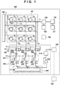
- the radiation imaging apparatus 100 is configured to capture an image formed by radiation.
- the image can be formed by radiation which has been emitted by a radiation source (not shown) and has passed through an object.
- the radiation can be, for example, an X-ray, ⁇ -ray, ⁇ -ray, or ⁇ -ray.
- the radiation imaging apparatus 100 includes a pixel array 101, driving circuit (driving unit) 102, readout circuit 103, detection circuit 120, reference bias potential generation circuit 126, control unit 106, calculation unit 130, and determination unit 131.
- the radiation imaging apparatus 100 can include a signal processing unit (processor) 105.
- the pixel array 101 includes a plurality of pixels PIX which are arranged two-dimensionally to constitute a plurality of rows and a plurality of columns.
- the pixels PIX are arranged to constitute three rows and three columns.
- a larger number of pixels PIX are arranged to constitute a larger number of rows and a larger number of columns.
- pixels of about 2,800 rows and about 2,800 columns are arranged.
- Each pixel PIX includes a conversion element 201 which converts radiation or light into charges, and a switching element T which outputs an electrical signal corresponding to the charges to a signal line Sig.
- the pixel PIX is configured to detect radiation.
- the conversion element 201 can be, for example, an indirect conversion element including a photoelectric conversion element S which converts light into charges, and a wavelength converter (scintillator) which converts radiation into light of a wavelength detectable by the photoelectric conversion element.
- the conversion element 201 can be a direct conversion element which directly converts radiation into charges.
- the photoelectric conversion element S can be, for example, a PIN photodiode which is mainly made of amorphous silicon and arranged on an insulating substrate such as a glass substrate.
- the photoelectric conversion element of the conversion element 201 is a PIN photodiode
- the conversion element 201 can have a capacitor Cs.
- the switching element T can be a transistor having a control terminal and two main terminals, for example, a thin film transistor (TFT).
- TFT thin film transistor
- One electrode of the conversion element 201 is electrically connected to one of the two main terminals of the switching element T.
- the other electrode of the conversion element 201 is electrically connected to a common bias line Vs.
- the detection circuit 120 supplies a bias potential VVs to the bias line Vs.
- the control terminal (gate) of the switching element T is connected to a driving line G which is driven by the driving circuit 102.
- the driving circuit 102 drives, to the active level, the driving line G of a row to be selected in the pixel array 101.
- an active-level driving signal is supplied to the gates of the switching elements T via the driving line G, the switching element T is turned on.
- signals corresponding to charges accumulated in the conversion elements 201 of the pixels PIX on the selected row are output in parallel to a plurality of signal lines Sig.
- the readout circuit 103 reads out the signals output to the signal lines Sig.
- the readout circuit 103 includes a plurality of amplifier circuits 207 and a multiplexer 208.
- the amplifier circuits 207 are arranged so that one amplifier circuit 207 corresponds to one signal line Sig.
- the amplifier circuits 207 amplify in parallel the signals output in parallel from the pixels PIX on the selected row to the plurality of signal lines Sig.
- Each amplifier circuit 207 can include, for example, an integrating amplifier 203, a variable amplifier 204 which amplifies a signal from the integrating amplifier 203, a sample and hold circuit 205 which samples and holds a signal from the variable amplifier 204, and a buffer amplifier 206.
- the integrating amplifier 203 can include, for example, an operational amplifier which amplifies a difference between a signal output to the signal line Sig and a reference potential Vref1 from a reference power supply 107, an integrating capacitor, and a reset switch.
- the amplification factor of the integrating amplifier 203 can be changed by changing the value of the integrating capacitor.
- the inverting input terminal of the operational amplifier receives a signal output to the signal line Sig, its non-inverting input terminal receives the reference voltage Vref1 from the reference power supply 107, and its output terminal is connected to the input terminal of the variable amplifier 204.
- the integrating capacitor and reset switch are parallel-connected between the inverting input terminal and output terminal of the operational amplifier.
- the sample and hold circuit 205 can be constructed by, for example, a sampling switch and sampling capacitor.
- the multiplexer 208 sequentially selects and outputs signals in parallel, said signals read out from the plurality of amplifier circuits 207 corresponding to the respective signal lines Sig.
- the readout circuit 103 can include a buffer amplifier 209 which buffers a signal from the multiplexer 208.
- the buffer amplifier 209 can function as an impedance converter.
- the readout circuit 103 can include an A/D converter 210.
- the A/D converter 210 can be arranged to convert an analog signal output from the buffer amplifier 209 into a digital signal.
- a signal output from the readout circuit 103 can be provided to the signal processing unit 105.
- the signal processing unit 105 can be configured to process a signal output from the readout circuit 103 and supply it to a computer 108.
- the signal processing unit 105 may be incorporated in the radiation imaging apparatus 100, as shown in Fig. 1 , or provided as an external apparatus outside the radiation imaging apparatus 100.
- the control unit 106 controls the overall operation of the radiation imaging apparatus 100 and generates, for example, a control signal for controlling the driving circuit 102 and a control signal for controlling the readout circuit 103.
- Fig. 1 does not show lines representing connections from the control unit 106 to the respective circuits.
- the driving circuit 102 turns on the switching elements T of the pixels PIX on a row from which signals should be read out.
- Control signals for controlling the readout circuit 103 can include, for example, a reset signal RC, sample and hold signal SH, and clock signal CLK.
- the reset signal RC is a signal which controls the reset switch of the integrating amplifier 203.
- the sample and hold signal SH is a signal which controls the sample and hold circuit 205.
- the clock signal CLK is a signal which controls the multiplexer 208.
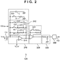
- the detection circuit 120 will be explained with reference to Fig. 2 .
- the detection circuit 120 detects a current (to be referred to as a bias current hereinafter) flowing through the bias line Vs, and provides, to the calculation unit 130, a bias current signal VSD representing this current. That is, the detection circuit 120 can function as an acquisition unit which acquires the bias current signal VSD.
- the detection circuit 120 can include, for example, a current-to-voltage conversion amplifier 310, voltage amplifier 320, filter circuit 330, and A/D converter 340.
- the current-to-voltage conversion amplifier 310 converts a current flowing through the bias line Vs into a voltage.
- the voltage amplifier 320 amplifies a signal (voltage signal) output from the current-to-voltage conversion amplifier 310.
- the voltage amplifier 320 can be constructed by, for example, an instrumentation amplifier.
- the filter circuit 330 is a filter which limits the band of a signal output from the voltage amplifier 320, and can be, for example, a low-pass filter.
- the A/D converter 340 supplies, to the calculation unit 130, the bias current signal VSD obtained by converting a signal (analog signal) output from the filter circuit 330 into a digital signal value.
- the detection circuit 120 more specifically, the current-to-voltage conversion amplifier 310 detects a current flowing through the bias line Vs, and supplies, to the bias line Vs, a potential corresponding to a reference bias potential Vs_ref supplied from the reference bias potential generation circuit 126.
- the current-to-voltage conversion amplifier 310 can be a transimpedance amplifier.
- the current-to-voltage conversion amplifier 310 includes, for example, an operational amplifier 311, and a feedback path 312 which is interposed between the inverting input terminal (second input terminal) and output terminal of the operational amplifier 311.
- the non-inverting input terminal (first input terminal) of the operational amplifier 311 receives the reference bias potential Vs_ref.
- the feedback path of the operational amplifier 311 can include the first path on which the inverting input terminal and output terminal are shorted by a resistor Rf1, the second path on which the inverting input terminal and output terminal are shorted by a resistor Rf2, and the third path on which the inverting input terminal and output terminal are shorted by a conductive line CL.
- a phase compensating capacitor Cf1 can be parallel-connected to the resistor Rf1.
- a phase compensating capacitor Cf2 can be parallel-connected to the resistor Rf2.
- the phase compensating capacitors Cf1 and Cf2 are effective for preventing, for example, oscillation of the current-to-voltage conversion amplifier 310.
- a switch SWC can be series-inserted in the path including the resistor Rf2.
- a switch SWB can be series-inserted in the path constructed by the conductive line CL.
- the control unit 106 controls the feedback impedance by supplying a control signal VSX to the detection circuit 120 to select a path to be enabled from a plurality of paths including the first, second, and third paths.
- the switch SWB When the switch SWB is closed, the third path constructed by the conductive line CL is enabled, and the first path including the resistor Rf1 and the second path including the resistor Rf2 are disabled.
- the switch SWB When the switch SWB is opened and the switch SWC is closed, the third path is disabled, and the first and second paths are enabled.
- a switch SWA and resistor R may be series-interposed between the inverting input terminal of the operational amplifier 311 and ground.
- a capacitor C may be interposed between the inverting input terminal of the operational amplifier 311 and ground.
- the current-to-voltage conversion amplifier 310 has the feedback path 312 and functions to generate, at the inverting input terminal (second input terminal) of the operational amplifier 311, a potential corresponding to the reference bias potential Vs_ref supplied to its non-inverting input terminal (first input terminal). More specifically, the current-to-voltage conversion amplifier 310 functions to generate, at the inverting input terminal of a differential amplifier circuit 211, almost the same potential as the reference bias potential Vs_ref supplied to its non-inverting input terminal.
- the control unit 106 controls the impedance (to be referred to as feedback impedance hereinafter) of the feedback path 312 of the current-to-voltage conversion amplifier 310.
- a high feedback impedance means a large gain of the current-to-voltage conversion amplifier 310.
- the feedback impedance limits the magnitude of a bias current I_Vs, and the potential of the bias line Vs may become unstable.
- the feedback impedance is controlled in accordance with the operation of the radiation imaging apparatus 100 such as a detection operation of detecting irradiation of the pixel array 101 with radiation, and an operation of reading out a signal from the pixel PIX. This will be explained in more detail.
- the calculation unit 130 calculates radiation information based on an output from the detection circuit 120, that is, the bias current signal VSD. Based on the radiation information, the determination unit 131 detects the start of irradiation of the pixel array 101 with radiation. In response to the detection, the control unit 106 controls the charge accumulation operation by the plurality of pixels PIX. That is, to quickly detect the start of irradiation of the pixel array 101 with radiation, the detection circuit 120 needs to detect, at high sensitivity, a current flowing through the bias line Vs. For this purpose, the feedback impedance is increased in the detection operation of detecting irradiation of the pixel array 101 with radiation.
- the control unit 106 controls the feedback impedance so that the feedback impedance in the detection operation of detecting irradiation with radiation becomes higher than that in the operation of reading out a signal from the pixel PIX.
- a case in which the value of the resistor Rf2 is smaller than that of the resistor Rf1 will be exemplified. In this case, when the second path including the resistor Rf2 is selected, the gain increases.
- control unit 106 opens the switch SWB in the detection operation of detecting irradiation with radiation, and closes it in the operation of reading out a signal from the pixel PIX.
- the state of the switch SWC is arbitrary in both the detection operation of detecting irradiation with radiation and the operation of reading out a signal from the pixel PIX.
- control unit 106 opens the switch SWB and closes the switch SWC in the detection operation of detecting irradiation with radiation, and closes the switch SWB in the operation of reading out a signal from the pixel PIX (the switch SWC can be opened or closed because the switch SWB is closed).
- the switch SWA and resistor R are not essential. However, when the switch SWA and resistor R are arranged, the switch SWA can be closed during the non-operating period of the detection circuit 120, and opened in the detection operation of detecting irradiation with radiation.
- the non-operating period of the detection circuit 120 can be a period excluding the detection operation of detecting irradiation with radiation, and an accumulation operation and image output operation (to be described later).
- the switch SWA may be closed or opened.
- the value of the resistor R may be larger than those of the resistors Rf1 and Rf2. For example, it is possible to set the resistor R to be 10 k ⁇ , the resistor Rf1 to be 1 k ⁇ , and the resistor Rf2 to be 1,050 ⁇ .
- the voltage amplifier 320 can be constructed as a variable gain amplifier.
- the gain of the voltage amplifier 320 can be changed by opening or closing a switch SWD.
- the operation of the radiation imaging apparatus 100 includes an initialization operation, accumulation operation, and readout operation.
- the initialization operation is an operation of initializing the plurality of pixels PIX of the pixel array 101 for each row.
- the accumulation operation is an operation of accumulating charges generated by irradiation with radiation in each pixel PIX of the pixel array 101.
- the readout operation is an operation of reading out, from the pixel array 101, a signal corresponding to charges accumulated in each pixel PIX of the pixel array 101 by irradiation of the pixel array 101 with radiation, and outputting the signal as an image (image signal).
- the operation shifts from the initialization operation to the accumulation operation when the determination unit 131 detects, based on an output from the detection circuit 120, the start of irradiation of the radiation imaging apparatus 100 with radiation.
- the operation shifts from the accumulation operation to the readout operation in response to, for example, the lapse of a predetermined time after the start of the accumulation operation.
- step S310 the control unit 106 starts the initialization operation.
- the control unit 106 repeats an operation of changing the driving lines G to the active level sequentially from the first to final rows, and changing the reset signal RC to the active level.
- the reset signal RC changes to the active level
- the integrating amplifier 203 changes to the voltage follower state, and the reference potential Vref1 is supplied to the signal line Sig.
- the switches T on a row on which the driving line G has been changed to the active level are turned on to initialize charges accumulated in the capacitors Cs of the conversion elements 201.
- Vg(0), Vg(1), Vg(2),..., Vg(Ys), Vg(Ys+1), ..., Vg(Y-1) are driving signals supplied to the driving lines G on the first to final rows of the pixel array 101.
- Y represents the number of rows of the pixel array 101, that is, the number of driving lines G.
- An operation until an active-level signal is supplied to the next driving line G after the control unit 106 starts supplying an active-level signal to one of the driving lines G will be called one initialization operation.
- a period until an active-level signal is supplied once to all the driving lines G will be called a frame.
- Y initialization operations are performed in one frame, and the pixels of one row are initialized by one initialization operation.
- the detection circuit 120 detects information correlated with the radiation dose to the pixel array 101, and supplies a detection signal corresponding to this information to the calculation unit 130.
- the detection circuit 120 detects the current I_Vs flowing through the bias line Vs as information correlated with the radiation dose to the pixel array 101, and supplies, to the calculation unit 130, the bias current signal VSD representing this current as a detection signal corresponding to this information.
- the determination unit 131 performs radiation detection processing. More specifically, the calculation unit 130 calculates radiation information based on the bias current signal VSD. Based on the radiation information, the determination unit 131 determines whether irradiation of the pixel array 101 with radiation has been started. In the embodiment, the determination unit 131 performs detection processing once every initialization operation. Alternatively, the determination unit 131 may perform detection processing once every plurality of initialization operations. In this case, the control unit 106 sets the feedback impedance in the detection operation of detecting irradiation with radiation, to be higher than the feedback impedance in the operation of reading out a signal from the pixel PIX.
- the control unit 106 continues to repeat the initialization operation until the start of irradiation of the pixel array 101 with radiation is detected (step S370). If the start of irradiation of the pixel array 101 with radiation is detected (YES in step S320), the control unit 106 starts the accumulation operation in step S330. That is, if the start of irradiation with radiation is detected (represented as "start of irradiation detect" in Fig. 4 ), the operation shifts from the initialization operation to the accumulation operation. Details of the detection processing in step S320 will be described later.
- step S340 the control unit 106 determines whether irradiation with radiation has ended.
- the radiation end determination method is not particularly limited. For example, when a predetermined time has elapsed after the start of the accumulation operation, it can be determined that irradiation with radiation has ended. Alternatively, the control unit 106 can detect the end of irradiation of the pixel array 101 with radiation based on the bias current signal VSD.
- the control unit 106 continues the accumulation operation until it determines that irradiation of the pixel array 101 with radiation has ended (step S380). If the control unit 106 determines that irradiation of the pixel array 101 with radiation has ended (YES in step S340), it starts the readout operation in step S350. That is, if it is determined that irradiation with radiation has ended (represented as "end of irradiation detected" in Fig. 4 ), the operation shifts from the accumulation operation to the readout operation. In the readout operation, signals are read out sequentially from pixels on the first row of the pixel array 101 to pixels on the final row.
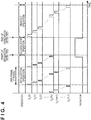
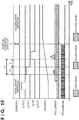
- Fig. 5 shows an example of the operation of the radiation imaging apparatus 100 when attention is paid to the timing to shift from the initialization operation to the accumulation operation.
- Vg(Ys-2), Vg(Ys-1), Vg(Ys), and Vg(Ys+1) are driving signals supplied to the driving lines G on the (Ys-2)th row to (Ys+1)th row of the pixel array 101.
- the switching element T is high active, is turned on when a high-level voltage (ON voltage) is applied to the driving line G, and is turned off when a low-level voltage (OFF voltage) is applied. Instead, the switching element T may be low active.
- the radiation imaging apparatus 100 can have the following features in regard to a bias current flowing through the bias line Vs.
- the sample value of the bias current signal VSD as a detection signal may be directly used.
- the calculation unit 130 calculates radiation information by processing a plurality of bias current signals VSD, and the determination unit 131 detects irradiation with radiation based on the radiation information. For example, when radiation information or the integral value of radiation information exceeds a predetermined threshold, the determination unit 131 determines that irradiation with radiation has been performed.
- TI is the driving cycle of the driving circuit 102. That is, the radiation imaging apparatus 100 performs one initialization operation in every time TI.
- TH is the time (to be referred to as the ON time hereinafter) when the driving circuit 102 supplies a high-level driving signal
- TL is the time (to be referred to as the OFF time hereinafter) when the driving circuit 102 supplies a low-level driving signal.
- the driving circuit 102 switches the driving signal of a certain driving line G from low level to high level, returns it to low level upon the lapse of the time TH, and starts the next initialization operation upon the lapse of the time TL of the same duration.
- TS is the sampling cycle of the A/D converter 340 of the detection circuit 120.
- the detection circuit 120 outputs two sample values of the bias current signal VSD in every initialization operation.
- a sample value output from the detection circuit 120 when the switching element T of the pixel PIX is ON will be called an effective value S.
- a sample value output from the detection circuit 120 when the switching element T of the pixel PIX is OFF will be called a noise value N.
- the calculation unit 130 can reduce external noise by calculating the difference between the effective value S and the noise value N, and can extract only the second signal as radiation information.
- the calculation unit 130 may calculate a radiation signal by using an effective value S and noise value N which have been sampled at close times.
- S(y) and N(y) are an effective value S and noise value N output in the yth (y is an arbitrary natural number) initialization operation, respectively.
- X(y) is radiation information used by the determination unit 131 in step S320 ( Fig. 3 ) to detect irradiation with radiation in the yth initialization operation.
- VSD bias current signal
- the method of reducing external noise in the above-described way will be called CDS (Correlated Double Sampling).
- the CDS calculation is not limited to the above-described calculation method.
- the calculation unit 130 may calculate X(y) by using sample values not adjacent to each other, such as S(y-1) and N(y-2).
- the calculation unit 130 may calculate radiation information after performing another arithmetical operation and differentiation/integration for a plurality of sample values of the bias current signal VSD.
- S(y) and N(y) in the yth sampling the sum of a plurality of sample values obtained by performing sampling a plurality of times (for example, eight times) in this period may be used.
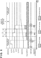
- FIG. 6 is different from the example of Fig. 5 in the sampling cycle TS of the A/D converter 340 of the detection circuit 120.
- the remaining points can be the same as those in the example of Fig. 5 , and a repetitive description thereof will be omitted.
- the sampling cycle TS of the A/D converter 340 is set to be shorter than 1/2 of the driving cycle TI of the driving circuit 102.
- the sample value of the bias current signal VSD sampled in the second half of the ON time TH is defined as the effective value S.
- the sample value of the bias current signal VSD sampled in the first half of the OFF time TL is defined as the noise value N. Similar to the example of Fig. 5 , S(y) and N(y) are an effective value S and noise value N output in the yth initialization operation, respectively.
- an external noise value contained in the effective value S and an external noise value contained in the noise value N can be brought close to each other. As a result, the influence of external noise in radiation information can be reduced.
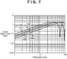
- Fig. 7 shows experimental results of calculating a noise reduction ratio when the sampling cycle TS is set to various values.
- the abscissa represents the frequency of external noise
- the ordinate represents the noise reduction ratio.
- Each of the ON time TH and OFF time TL of the driving signal is set to be 16 ⁇ sec.
- curves 701, 702, 703, and 704 indicate noise reduction ratios at respective frequencies when the sampling cycle TS is set to be 16 ⁇ sec, 10.6 ⁇ sec, 8 ⁇ sec, and 5.3 ⁇ sec, respectively.
- noise is reduced more efficiently as the sampling cycle TS is shorter.
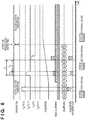
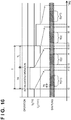
- Fig. 8 is different from the example of Fig. 5 in the driving timing (ON time TH and OFF time TL) by the driving circuit 102, and the sampling cycle TS of the A/D converter 340 of the detection circuit 120.
- the remaining points can be the same as those in the example of Fig. 5 , and a repetitive description thereof will be omitted.
- the OFF time TL is longer than the ON time TH.
- the driving circuit 102 operates so that the OFF time TL becomes triple of the ON time TH.
- the sampling cycle TS is set to be equal to the ON time TH.
- the detection circuit 120 outputs one effective value S and three noise values N in one reset operation.
- S(y), N1(y), N2(y), and N3(y) are an effective value S and three noise values N output in the yth (y is an arbitrary natural number) initialization operation, respectively.
- X(y) is radiation information used by the determination unit 131 in step S320 ( Fig. 3 ) to detect irradiation with radiation in the yth initialization operation. Note that N1(y), N2(y), and N3(y) are aligned sequentially from a value sampled at earlier time.
- the noise values N are weighted. More specifically, the noise values N are multiplied by different coefficients.
- X(y) is obtained by repeating subtraction between adjacent values for one effective value S and a plurality of noise values N obtained in the same initialization operation.
- the calculation unit 130 performs subtraction between adjacent sample values in the same initialization operation, sets the difference between the effective value S and the noise value N as a new effective value S, and sets the difference between the noise values N as a new noise value N.
- the calculation unit 130 repeats this calculation until one value is obtained.
- n noise values N are obtained in one initialization operation, the calculation unit 130 repeats the above calculation by n stages. This processing is given by:
- the calculation unit 130 calculates radiation information by using one effective value S and three noise values N obtained successively after the effective value S. Instead, the calculation unit 130 may calculate radiation information by using one effective value S and three noise values N obtained successively before the effective value S as per:
- X y S y ⁇ 3 ⁇ N 3 y ⁇ 1 ⁇ 3 ⁇ N 2 y ⁇ 1 + N 1 y ⁇ 1
- X(y) is obtained by the same calculation as that of equation (7).
- the calculation unit 130 calculates radiation information based on one effective value S and the weighted values of six noise values N obtained successively before and after the effective value S.
- a noise value N sampled nearer the timing of switching between the effective value S and the noise value N is multiplied by a larger weight.
- a large weight means that the influence on radiation information is large, and can mean that, for example, the absolute value of the coefficient of the noise value N is large. This also applies to the following example.
- Fig. 9 shows the experimental results of calculating a noise reduction ratio when the radiation information X(y) is calculated by various methods.
- the abscissa represents the frequency of external noise
- the ordinate represents the noise reduction ratio.
- the ON time TH of the driving signal is set to be 8 ⁇ sec
- the OFF time TL is set to be 24 ⁇ sec.
- curves 801, 802, 803, and 804 indicate noise reduction ratios at respective frequencies when the radiation information X(y) is calculated by equations (5), (7), (8), and (10) above, respectively.
- Fig. 9 also shows the curve 701 in Fig. 7 .
- noise is reduced efficiently by weighting a plurality of noise values N to calculate radiation information.
- Radiation information in each of equations (8) to (10) may be calculated by sequentially performing subtraction between adjacent sample values, or by adding or subtracting a value obtained by multiplying a sample value by a coefficient according to each of these equations. This also applies to a case in which radiation information is calculated according to an equation to be described later.
- External noise which flows when a pressure or shock is applied to the radiation imaging apparatus 100 can take a value which is 10 to 100 times larger than a current flowing through the bias line Vs upon irradiation with radiation.
- the dynamic range of the detection circuit 120 can be set so that sampling can be performed without saturating external noise.
- control unit 106 may be configured to multiply radiation information and a threshold by integers so that radiation information is calculated by only addition, subtraction, and multiplication, in order to reduce generation of a quantization error caused by division.
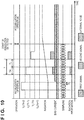
- Fig. 10 is different from the example of Fig. 5 in the sampling cycle TS of the A/D converter 340 of the detection circuit 120.
- the remaining points can be the same as those in the example of Fig. 5 , and a repetitive description thereof will be omitted.
- the OFF time TL and ON time TH are equal to each other.
- the sampling cycle TS is set to be shorter than the ON time TH.
- the sampling cycle TS is set to be 1/3 of the ON time TH.
- the detection circuit 120 outputs three effective values S and three noise values N in one reset operation.
- S1(y), S2(y), S3(y), N1(y), N2(y), and N3(y) are three effective values S and three noise values N output in the yth (y is an arbitrary natural number) initialization operation, respectively.
- X(y) is radiation information used by the control unit 106 in step S320 ( Fig. 3 ) to detect irradiation with radiation in the yth initialization operation. Note that S1(y), S2(y), S3(y), N1(y), N2(y), and N3(y) are aligned sequentially from a value sampled at earlier time.
- the effective values S and noise values N are weighted. More specifically, the effective values S and noise values N are multiplied by different coefficients.
- D1 to D3 be the differences each between the average of the effective values S and the average of the noise values N, this processing is given by:
- the calculation unit 130 calculates radiation information for the yth initialization operation based on values obtained by weighting three effective values S obtained in the yth initialization operation, and six noise values N obtained before and after these effective values S.
- a noise value N sampled nearer the timing of switching between the effective value S and the noise value N is multiplied by a larger weight.
- Fig. 11 shows the experimental results of calculating a noise reduction ratio when the radiation information X(y) is calculated by various methods.
- the abscissa represents the frequency of external noise
- the ordinate represents the noise reduction ratio.
- the ON time TH of the driving signal is set to be 16 ⁇ sec
- the OFF time TL is set to be 16 ⁇ sec.
- the sampling time TS is set to be 5.3 ⁇ sec.
- curves 1101 and 1102 indicate noise reduction ratios at respective frequencies when the radiation information X(y) is calculated based on equation (14) and the average of equations (14) and (15), respectively.
- Fig. 11 also shows the curve 701 in Fig. 7 .
- noise is reduced efficiently by weighting a plurality of noise values N and calculating radiation information.
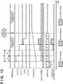
- Fig. 12 is different from the example of Fig. 5 in the sampling cycle TS of the A/D converter 340 of the detection circuit 120, and the OFF time TL.
- the remaining points can be the same as those in the example of Fig. 5 , and a repetitive description thereof will be omitted.
- the driving cycle TI of the driving circuit 102 is equal to the ON time TH, and the OFF time TL is 0. That is, in one initialization operation, the driving circuit 102 maintains a driving signal to the driving line G at the active level.
- the sampling cycle TS is set to be shorter than the ON time TH.
- the sampling cycle TS is set to be 1/3 of the ON time TH.
- the detection circuit 120 outputs three effective values S in one reset operation.
- S1(y), S2(y), and S3(y) are three effective values S output in the yth (y is an arbitrary natural number) initialization operation, respectively.
- X(y) is radiation information used by the determination unit 131 in step S320 ( Fig. 3 ) to detect irradiation with radiation in the yth initialization operation. Note that S1(y), S2(y), and S3(y) are aligned sequentially from a value sampled at earlier time.
- D1 to D3 be the differences each between the average of the effective values S obtained in the yth initialization and the average of the effective values S obtained in the (y-1)th initialization, this processing is given by:
- Equation (16) can have the same noise reduction characteristic as that of equation (14) because the same calculation as equation (14) is performed for external noise.
- the radiation information X(y) obtained by equation (16) is a value obtained by weighting a plurality of effective values S obtained in successive initialization operations and calculating a difference. If this value exceeds a threshold, the determination unit 131 detects irradiation with radiation.
- Fig. 13 is different from the example of Fig. 5 in the driving timing (ON time TH and OFF time TL) by the driving circuit 102.
- the remaining points can be the same as those in the example of Fig. 5 , and a repetitive description thereof will be omitted.
- the driving circuit 102 superposes the trailing and rising of two successively supplied driving signals. For example, the driving circuit 102 superposes the trailing of a driving signal in an odd-numbered initialization operation and the rising of a driving signal in an even-numbered initialization operation.
- the driving circuit 102 sets the OFF time TL in an odd-numbered initialization operation to be 0.
- the driving cycle TI differs between odd- and even-numbered initialization operations.
- the trailing of a driving signal supplied to the driving line G on the (Ys-1)th row and the rising of a driving signal supplied to the driving line G on the Ysth row overlap each other.
- the detection circuit 120 When the sampling cycle TS of the A/D converter 340, the ON time TH, and the OFF time TL are set to be equal to each other, the detection circuit 120 outputs one effective value S in an odd-numbered reset operation, and outputs one effective value S and one noise value N in an even-numbered reset operation.
- S(y) is an effective value S output in the yth (y is an arbitrary odd number) initialization operation.
- S(y+1) and N(y+1) are an effective value S and noise value N output in the immediately succeeding (y+1)th initialization operation, respectively.
- X(y) is radiation information used by the determination unit 131 in step S320 ( Fig. 3 ) to detect irradiation with radiation in the yth initialization operation.
- a current (second signal) flowing through the bias line Vs in proportion to the amount of charges accumulated in the conversion element 201 of the pixel PIX until the switching element T of a pixel PIX irradiated with radiation is turned on has the following property. That is, this current is a spike-like current which starts flowing at the same time (at time t0) as the rising of the driving signal, peaks when the switching element T is turned on (at time t1), and then stops flowing (at time t2).
- the time until the switching element T is turned on after the rising of the driving signal is determined by the time constant which, in turn, is defined by the resistance and the parasitic capacitance of the driving line G.
- the detection circuit 120 samples a current flowing through the bias line Vs upon the lapse of a delay time TD (at time t1) after the driving circuit 102 activates the driving signal in one initialization operation (at time t0).
- a sample value output from the detection circuit 120 in this case serves as the effective value S.
- the detection circuit 120 samples a current flowing through the bias line Vs upon the lapse of the same delay time TD (at time t4) after the driving circuit 102 inactivates the driving signal in one initialization operation (at time t3).
- a sample value output from the detection circuit 120 in this case serves as the noise value N.
- the method of calculating radiation information from the effective value S and noise value N can be any one of the aforementioned methods.
- switching noise of the switching element T starts flowing at the same time as the rising or trailing of the driving signal and does not flow after the switching element T is switched to the ON state or OFF state. For this reason, the influence of switching noise on a radiation signal can be reduced by performing sampling by the detection circuit 120 at the above-mentioned timings.
- the delay time TD is set to perform sampling at the timing (for example, time t1) of the peak of a current flowing through the bias line Vs.
- the delay time TD is determined based on the time constant of the driving line G and the time constant of the bias line Vs.
- the delay time TD may be determined further based on the processing time of a circuit at the preceding stage of the A/D converter 340 in the detection circuit 120.
- the control unit 106 pre-samples a current flowing through the bias line Vs at a time interval shorter than the sampling interval in Fig. 14 .
- the manufacturer of the radiation imaging apparatus 100 irradiates the radiation imaging apparatus 100 with test radiation during pre-sampling.
- the control unit 106 stores, as the delay time TD, the time between the rising time of the driving signal in one initialization operation and the sampling time when the sample value of the bias current signal VSD becomes maximum in this initialization operation.
- a current flowing through the bias line Vs by dark charges accumulated in the pixel PIX may be used.
- the control unit 106 maintains at low level a driving signal supplied from the driving circuit 102, and waits for accumulation of dark charges in the pixel PIX. After that, the control unit 106 starts the initialization operation shown in Fig. 15 .
- the switching element T is turned on, a current corresponding to the dark charges flows through the bias line Vs. Based on this current, the control unit 106 determines the delay time TD.
- the time constant of the driving line G, the time constant of the bias line Vs, and the processing time of the detection circuit 120 may change depending on aging deterioration after product shipment and the temperature of the use environment. Considering this, the delay time TD may be determined even after product shipment.
- the radiation imaging apparatus 100 may be configured to be able to switch between an adjustment mode in which pre-sampling mentioned above is executed, and a normal mode in which normal sampling is executed. In the adjustment mode, the user of the radiation imaging apparatus 100 irradiates the radiation imaging apparatus 100 with test radiation. Instead, the radiation imaging apparatus 100 may shift to the operation mode in which dark charges are accumulated.
- the control unit 106 stores, as the delay time TD, the time between the rising time of the driving signal in one initialization operation and the sampling time when the sample value of the bias current signal VSD becomes maximum in this initialization operation.
- the detection circuit 120 performs sampling in accordance with the stored delay time TD.
- sampling has been described based on the driving timing of the driving circuit 102 shown in Fig. 5 . However, sampling may be performed upon the lapse of the delay time similarly at the driving timing in Fig. 12 or 13 .
- Fig. 16 is different from the example of Fig. 5 in the sampling cycle TS of the A/D converter 340 of the detection circuit 120.
- the remaining points can be the same as those in the example of Fig. 5 , and a repetitive description thereof will be omitted.
- the sampling cycle TS 1 ⁇ sec.
- the detection circuit 120 outputs 32 bias current signals VSD in one initialization operation.
- the yth initialization operation assume that a driving signal supplied to the driving line G on the Ysth row is switched to high level at time t0. Then, assume that the influence of switching of the driving signal to high level on an analog signal input to the A/D converter 340 of the detection circuit 120 appears at time t1.
- 16 sample values output from the detection circuit 120 at an interval between time t1 and time t5 correspond to a case in which the switching element T is ON in the yth initialization operation.
- the calculation unit 130 uses, as an effective value S(y) for the yth initialization operation, the sum of eight intermediate sample values output at an interval between time t3 and time t4, out of these 16 sample values.
- 16 sample values output from the detection circuit 120 at an interval between time t5 and time t9 correspond to a case in which the switching element T is OFF in the yth initialization operation.
- the calculation unit 130 uses, as a noise value N(y) for the yth initialization operation, the sum of eight intermediate sample values output at an interval between time t7 and time t8, out of these 16 sample values. Then, the calculation unit 130 calculates radiation information according to equations (1) to (3) described above.
- Fig. 17 is different from the example of Fig. 4 in the timing of the driving signal supplied from the driving circuit 102 to the driving line G in the initialization operation.
- the remaining points can be the same as those in the example of Fig. 4 , and a repetitive description thereof will be omitted.
- the driving circuit 102 supplies high-level driving signals sequentially to odd-numbered driving lines G counted from one side of the pixel array 101, and then supplies high-level driving signals sequentially to even-numbered driving lines G.
- the radiation imaging apparatus 100 performs the initialization operation for the pixels PIX.
- the radiation information is partially lost from the pixel row initialized during this period.
- pixel rows from which the radiation information is partially lost can be distributed in image data by preventing temporally successive resetting of adjacent pixel rows, as in the example of Fig. 17 . This makes it easy to correct the image data by complementing the lost radiation information using information of pixel rows from which radiation information has been normally acquired.
- the driving circuit 102 supplies high-level driving signals simultaneously to the two driving lines G.
- a current proportional to charges accumulated in pixels of two rows flows through the bias line Vs.
- the S/N ratio of the bias current signal can be increased.
- the two driving lines G are simultaneously driven in the example of Fig. 17
- a driving line group including an arbitrary number of (two or more) driving lines G may be driven.
- the driving lines G to be driven simultaneously may be adjacent to each other.
- the radiation imaging apparatus 100 may be configured to be able to change the number of driving lines to be driven simultaneously in accordance with an input from the user. In this case, as the number of driving lines to be driven simultaneously increases, switching noise also increases, so the control unit 106 may switch the gain of the detection circuit 120 in accordance with the number of driving lines.
- the present invention is not limited to the above-described embodiments.
- the ON time TH may be longer than the OFF time TL.
- a plurality of effective values S and one noise value N may be sampled.
- the calculation unit 130 may calculate radiation information by using one or more of a plurality of effective values S obtained in one initialization operation and one or more of a plurality of noise values N.
- the calculation unit 130 need not calculate radiation information by using both the effective value S and noise value N, and may calculate radiation information by using a plurality of effective values S or calculate radiation information by using a plurality of noise values N. As described with reference to Fig.
- the calculation unit 130 may calculate, as radiation information, the difference between an effective value S obtained when the pixel array 101 is irradiated with radiation, and a previously acquired effective value S obtained when the pixel array 101 is not irradiated with radiation. Similarly, the calculation unit 130 may calculate, as radiation information, the difference between a noise value N obtained when the pixel array 101 is irradiated with radiation, and a previously acquired noise value N obtained when the pixel array 101 is not irradiated with radiation.
- the calculation unit 130 calculates radiation information based on sample values acquired a plurality of times for the bias current signal VSD supplied from the detection circuit 120. By comparing the radiation information with a threshold, the determination unit 131 can determine the presence/absence of irradiation with radiation.
- the weights on the effective value S and noise value N are not limited to values determined by the above-described methods. One or more effective values S and one or more noise values N may be multiplied by arbitrary weights, respectively.
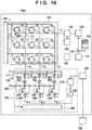
- the overall arrangement of a radiation imaging apparatus 1800 will be described with reference to Fig. 18 .
- the radiation imaging apparatus 1800 is different from the radiation imaging apparatus 100 of Fig. 1 in that it further includes a memory 132 and adder 133.
- the remaining arrangement can be the same as the embodiment of the radiation imaging apparatus 100, and a repetitive description thereof will be omitted.
- the memory 132 can accumulate pieces of radiation information output from a calculation unit 130 for one frame (Y pieces of radiation information in the above-described example), and outputs them to the adder 133 by FIFO in the order of storage.
- the adder 133 subtracts radiation information output from the memory 132, from radiation information output from the calculation unit 130, and supplies the difference to a determination unit 131. For example, when the calculation unit 130 outputs radiation information X(y) obtained for the yth initialization operation, X(y) - X(y-Y) is supplied to the determination unit 131. That is, the difference from radiation information of an immediately preceding frame is supplied to the determination unit 131.
- the present inventors have found out that the switching noise amount differs between the driving lines G, but the reproducibility is high for a single driving line G. For this reason, switching noise can be effectively reduced by subtracting radiation information obtained by driving a certain driving line G in advance, from radiation information obtained by driving the same driving line G, as described above. This will be called frame correction.
- radiation information of an immediately preceding frame is subtracted from the current radiation information.
- radiation information before k frames may be subtracted, or the average (simple average or weighted average) of pieces of radiation information of a plurality of frames for the same driving line G may be subtracted.
- the memory 132 may be interposed not between the calculation unit 130 and the determination unit 131, but between a detection circuit 120 and the calculation unit 130, and subtraction may be performed at the stage of a bias current signal VSD supplied to the calculation unit 130. In this manner, when the difference is calculated between frames, switching noise can be effectively reduced by making constant the driving timing of the driving signal and the sample and hold timing of an A/D converter 340 for each frame.
- clocks may be supplied from a common clock generator to a driving circuit 102 and the A/D converter 340.
- the radiation imaging apparatus 1800 may include an integrating circuit 500 shown in Fig. 21 between the adder 133 and the determination unit 131.
- the integrating circuit 500 can include a shift register 501, adders 502a and 502b, and registers 503a and 503b which hold integral values.
- the determination unit 131 can include comparators 504a and 504b, and an OR circuit 505.
- X is the latest radiation information output from the adder 133.
- the adder 502a and register 503a constitute one integrator, and the adder 502b and register 503b constitute another integrator.
- the integral value can be calculated in an integral interval determined by the tap (readout position) of the shift register 501. Since calculation of the integral value is completed by one clock, the time taken to determine the start of irradiation can be greatly shortened.
- M comparators like the comparators 504a and 504b are also arranged. The comparator compares the mth integral value Sum[m] with the mth threshold T[m]. If Sum[m] > T[m] in any comparator, it can be determined by the OR circuit 505 that irradiation with radiation has started. If Sum[m] ⁇ T[m] in all the comparators, it is determined that irradiation with radiation has not been performed.
- an adder and comparator are arranged for each register which holds an integral value.
- a plurality of registers may share one adder and one comparator.
- the shift register 501 can be constructed by a single block, but may be divided into a plurality of blocks.
- the plurality of blocks constructing the shift register 501 can be mounted in, for example, different memory segments on an FPGA.
- the arrangement shown in Fig. 21 may be implemented by software.
- the determination unit 131 determines that irradiation with radiation has been performed. Also, an arrangement can be adopted, in which CDS is performed for the sum of a plurality of effective values S and the sum of a plurality of noise values N, as shown in Fig. 10 . These calculations are not in particular order. However, to decrease the amount of data to process, it is also possible to perform signal processing in the order of addition, CDS, frame correction, and integration, and then perform comparison with a predetermined threshold.
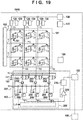
- the radiation imaging apparatus 1900 is different from the radiation imaging apparatus 100 of Fig. 1 in that a bias line Vs is arranged for each pixel column, and a plurality of detection circuits 120 and a plurality of reference bias potential generation circuits 126 are arranged.
- the detection circuit 120 and reference bias potential generation circuit 126 are arranged for one bias line Vs.
- the remaining arrangement can be the same as the embodiment of the radiation imaging apparatus 100, and a repetitive description thereof will be omitted.
- the radiation imaging apparatus 1900 may include a memory 132 between a calculation unit 130 and a determination unit 131, similar to the radiation imaging apparatus 1800.
- the radiation imaging apparatus 1900 may include the detection circuit 120 and reference bias potential generation circuit 126 for every two or more bias lines Vs, instead of including the detection circuit 120 and reference bias potential generation circuit 126 for every bias line Vs.
- each bias line Vs is connected to pixels PIX which are equal in the length of a portion of the driving line G that extends from the driving circuit 102 to the switching element T, and which are aligned in the column direction.
- the detection circuit 120 and reference bias potential generation circuit 126 are arranged for each bias line Vs. In this case, the position of the peak of the second signal of the bias current may differ between the detection circuits 120.
- a delay time TD is determined by the above-described method for each detection circuit 120, and sampling is performed.
- Bias current signals VSD output from the respective detection circuits 120 are added to supply the sum to the calculation unit 130. Subsequent processing is the same as the embodiment of the radiation imaging apparatus 100, and a repetitive description thereof will be omitted. In this embodiment, the S/N ratio of the bias current signal can be further increased.
- a radiation imaging apparatus will be explained.
- the arrangement of the radiation imaging apparatus according to the embodiment can be the same as that of the radiation imaging apparatus according to any one of the above-described embodiments, and a radiation imaging apparatus 100 will be exemplified.
- the radiation imaging apparatus 100 measures noise generated when irradiation with radiation is performed, and changes the operation settings of the radiation imaging apparatus 100 based on the noise amount.
- These operation settings can be settings about the radiation detection operation in Fig. 3 , including the aforementioned ON time TH, OFF time TL, sampling cycle TS, equations for calculating radiation information, the number of driving lines G to be driven simultaneously, and a threshold to be compared with radiation information by a determination unit 131.
- a control unit 106 starts noise measurement.
- the control unit 106 may start noise measurement in response to an input from the user of the radiation imaging apparatus 100, or automatically start it after power-on of the radiation imaging apparatus 100.
- step S2020 the control unit 106 determines whether the noise measurement end condition has been satisfied.
- the noise measurement end condition may be the lapse of a predetermined time after the start of noise measurement, or acceptance of an input indicating the end from the user. If the noise measurement end condition has not been satisfied (NO in step S2020), the control unit 106 continues the initialization operation in step S2030. Although this initialization operation is the same as that in step S370 of Fig. 3 , the determination unit 131 stores radiation information supplied from the calculation unit 130, instead of determining the presence/absence of irradiation with radiation. For example, the determination unit 131 can store the latest radiation information of one frame. Then, the process returns to step S2020, and the control unit 106 determines whether the noise measurement end condition has been satisfied.
- the control unit 106 determines in step S2040 whether radiation information stored in the determination unit 131 is larger than a predetermined value.
- the radiation imaging apparatus 100 is not irradiated with radiation, so the radiation information represents noise which remains even after the above-mentioned CDS operation.
- the control unit 106 changes the operation settings in step S2050.
- control unit 106 may increase the threshold used by the determination unit 131 in step S320 for comparison with radiation information, or change the driving cycle of a driving circuit 102 to reduce the influence of external noise in accordance with the frequency characteristic of detected noise. If the noise is not larger than the predetermined value (NO in step S2040), the control unit 106 shifts to step S310 of Fig. 3 , and starts the imaging standby start state. In this case, the control unit 106 may change the operation settings. For example, the control unit 106 may decrease the threshold used by the determination unit 131 in step S320 for comparison with radiation information.
- step S2050 the process may further return to step S2020 to repeat noise measurement. If the noise value greatly exceeds the predetermined value in step S2040, the control unit 106 may present this result to the user. In this case, the control unit 106 may inhibit shift to the imaging standby state.
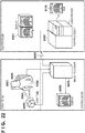
- Fig. 22 is a view showing an example in which the radiation imaging apparatus according to the present invention is applied to an X-ray diagnostic system (radiation imaging system).
- the radiation imaging system includes a radiation imaging apparatus 6040 (corresponding to one of the radiation imaging apparatuses 100, 1800, and 1900), and an image processor 6070 which processes a signal output from the radiation imaging apparatus 6040.
- X-rays 6060 generated by an X-ray tube (radiation source) 6050 pass through a chest 6062 of a patient or object 6061 and enter the radiation imaging apparatus 6040.
- the incident X-rays include information about the inside of the body of the object 6061.
- the image processor (processor) 6070 processes a signal (image) output from the radiation imaging apparatus 6040, and can, for example, display an image on a display 6080 in a control room based on a signal obtained by the processing.
- the image processor 6070 can transfer the signal obtained by the processing to a remote place via a transmission path 6090. Accordingly, the image can be displayed on a display 6081 installed in a doctor room or the like at another place, and the image can be recorded on a recording medium such as an optical disk.
- the recording medium can be a film 6110. In this case, a film processor 6100 records the image on the film 6110.
- Embodiments of the present invention can also be realized by a computer of a system or apparatus that reads out and executes computer executable instructions recorded on a storage medium (e.g., non-transitory computer-readable storage medium) to perform the functions of one or more of the above-described embodiment(s) of the present invention, and by a method performed by the computer of the system or apparatus by, for example, reading out and executing the computer executable instructions from the storage medium to perform the functions of one or more of the above-described embodiment(s).
- the computer may comprise one or more of a central processing unit (CPU), micro processing unit (MPU), or other circuitry, and may include a network of separate computers or separate computer processors.
- the computer executable instructions may be provided to the computer, for example, from a network or the storage medium.
- the storage medium may include, for example, one or more of a hard disk, a random-access memory (RAM), a read only memory (ROM), a storage of distributed computing systems, an optical disk (such as a compact disc (CD), digital versatile disc (DVD), or Blu-ray Disc (BD)TM), a flash memory device, a memory card, and the like.
Landscapes
- Engineering & Computer Science (AREA)
- Health & Medical Sciences (AREA)
- Life Sciences & Earth Sciences (AREA)
- Physics & Mathematics (AREA)
- Medical Informatics (AREA)
- Molecular Biology (AREA)
- High Energy & Nuclear Physics (AREA)
- Signal Processing (AREA)
- Multimedia (AREA)
- General Physics & Mathematics (AREA)
- General Health & Medical Sciences (AREA)
- Nuclear Medicine, Radiotherapy & Molecular Imaging (AREA)
- Heart & Thoracic Surgery (AREA)
- Radiology & Medical Imaging (AREA)
- Surgery (AREA)
- Animal Behavior & Ethology (AREA)
- Pathology (AREA)
- Public Health (AREA)
- Veterinary Medicine (AREA)
- Optics & Photonics (AREA)
- Biophysics (AREA)
- Biomedical Technology (AREA)
- Spectroscopy & Molecular Physics (AREA)
- Power Engineering (AREA)
- Mathematical Physics (AREA)
- Toxicology (AREA)
- Electromagnetism (AREA)
- Condensed Matter Physics & Semiconductors (AREA)
- Computer Hardware Design (AREA)
- Microelectronics & Electronic Packaging (AREA)
- Measurement Of Radiation (AREA)
- Transforming Light Signals Into Electric Signals (AREA)
- Apparatus For Radiation Diagnosis (AREA)
- Solid State Image Pick-Up Elements (AREA)
Priority Applications (1)
| Application Number | Priority Date | Filing Date | Title |
|---|---|---|---|
| EP18155827.1A EP3349434B1 (en) | 2013-02-28 | 2014-02-27 | Radiation imaging apparatus and radiation imaging system |
Applications Claiming Priority (1)
| Application Number | Priority Date | Filing Date | Title |
|---|---|---|---|
| JP2013040030A JP5934128B2 (ja) | 2013-02-28 | 2013-02-28 | 放射線撮像装置及び放射線撮像システム |
Related Child Applications (2)
| Application Number | Title | Priority Date | Filing Date |
|---|---|---|---|
| EP18155827.1A Division-Into EP3349434B1 (en) | 2013-02-28 | 2014-02-27 | Radiation imaging apparatus and radiation imaging system |
| EP18155827.1A Division EP3349434B1 (en) | 2013-02-28 | 2014-02-27 | Radiation imaging apparatus and radiation imaging system |
Publications (3)
| Publication Number | Publication Date |
|---|---|
| EP2773103A2 EP2773103A2 (en) | 2014-09-03 |
| EP2773103A3 EP2773103A3 (en) | 2015-06-10 |
| EP2773103B1 true EP2773103B1 (en) | 2018-04-11 |
Family
ID=50159167
Family Applications (2)
| Application Number | Title | Priority Date | Filing Date |
|---|---|---|---|
| EP14157067.1A Active EP2773103B1 (en) | 2013-02-28 | 2014-02-27 | Radiation imaging apparatus and radiation imaging system |
| EP18155827.1A Active EP3349434B1 (en) | 2013-02-28 | 2014-02-27 | Radiation imaging apparatus and radiation imaging system |
Family Applications After (1)
| Application Number | Title | Priority Date | Filing Date |
|---|---|---|---|
| EP18155827.1A Active EP3349434B1 (en) | 2013-02-28 | 2014-02-27 | Radiation imaging apparatus and radiation imaging system |
Country Status (4)
| Country | Link |
|---|---|
| US (2) | US9470800B2 (ja) |
| EP (2) | EP2773103B1 (ja) |
| JP (1) | JP5934128B2 (ja) |
| KR (1) | KR101690364B1 (ja) |
Families Citing this family (57)
| Publication number | Priority date | Publication date | Assignee | Title |
|---|---|---|---|---|
| JP5814621B2 (ja) | 2011-05-24 | 2015-11-17 | キヤノン株式会社 | 撮像装置及びその制御方法、並びに、撮像システム |
| JP6016673B2 (ja) | 2013-02-28 | 2016-10-26 | キヤノン株式会社 | 放射線撮像装置および放射線撮像システム |
| JP5986524B2 (ja) | 2013-02-28 | 2016-09-06 | キヤノン株式会社 | 放射線撮像装置および放射線撮像システム |
| JP6238577B2 (ja) | 2013-06-05 | 2017-11-29 | キヤノン株式会社 | 放射線撮像装置及び放射線撮像システム |
| US9737271B2 (en) | 2014-04-09 | 2017-08-22 | Canon Kabushiki Kaisha | Radiation imaging apparatus and control method of the same |
| JP6362421B2 (ja) | 2014-05-26 | 2018-07-25 | キヤノン株式会社 | 放射線撮像装置、その制御方法およびプログラム |
| JP6577700B2 (ja) | 2014-06-30 | 2019-09-18 | キヤノン株式会社 | 放射線検出装置、その制御方法、放射線撮影装置、およびプログラム |
| DE102014224449A1 (de) * | 2014-11-28 | 2016-06-02 | Forschungszentrum Jülich GmbH | Szintillationsdetektor mit hoher Zählrate |
| US9912881B2 (en) * | 2014-12-09 | 2018-03-06 | Canon Kabushiki Kaisha | Apparatus, system, and method of controlling apparatus |
| JP6366542B2 (ja) * | 2015-06-17 | 2018-08-01 | キヤノン株式会社 | 放射線撮像装置、放射線撮像システムおよび照射開始検出方法 |
| JP6572025B2 (ja) | 2015-07-02 | 2019-09-04 | キヤノン株式会社 | 放射線撮像装置及びその制御方法 |
| JP6573377B2 (ja) | 2015-07-08 | 2019-09-11 | キヤノン株式会社 | 放射線撮像装置、その制御方法及びプログラム |
| JP6573378B2 (ja) | 2015-07-10 | 2019-09-11 | キヤノン株式会社 | 放射線撮像装置、その制御方法及びプログラム |
| JP6643871B2 (ja) | 2015-11-13 | 2020-02-12 | キヤノン株式会社 | 放射線撮像装置およびフォトンカウンティングの方法 |
| JP6587517B2 (ja) | 2015-11-13 | 2019-10-09 | キヤノン株式会社 | 放射線撮像システム |
| JP6663210B2 (ja) | 2015-12-01 | 2020-03-11 | キヤノン株式会社 | 放射線撮像装置及びその制御方法 |
| JP6643909B2 (ja) | 2016-01-27 | 2020-02-12 | キヤノン株式会社 | 放射線撮像装置、その制御方法及びプログラム |
| WO2017145816A1 (ja) * | 2016-02-24 | 2017-08-31 | ソニー株式会社 | 光学測定器、フローサイトメータ、および放射線計数器 |
| JP6706963B2 (ja) | 2016-04-18 | 2020-06-10 | キヤノン株式会社 | 放射線撮像装置、放射線撮像システム、及び、放射線撮像装置の制御方法 |
| JP2017205229A (ja) * | 2016-05-17 | 2017-11-24 | キヤノン株式会社 | 放射線撮影装置およびその制御方法 |
| JP6596184B2 (ja) | 2016-09-08 | 2019-10-23 | コーニンクレッカ フィリップス エヌ ヴェ | 放射線ディテクター及びx線像形成システム |
| JP6871717B2 (ja) | 2016-11-10 | 2021-05-12 | キヤノン株式会社 | 放射線撮像装置、放射線撮像システムおよび放射線撮像方法 |
| JP6775408B2 (ja) * | 2016-12-20 | 2020-10-28 | キヤノン株式会社 | 放射線撮像装置及び放射線撮像システム |
| JP6461212B2 (ja) | 2017-02-01 | 2019-01-30 | キヤノン株式会社 | 放射線撮像装置及び放射線撮像システム |
| JP6974948B2 (ja) | 2017-02-10 | 2021-12-01 | キヤノン株式会社 | 放射線撮像装置および放射線撮像方法 |
| JP6929104B2 (ja) | 2017-04-05 | 2021-09-01 | キヤノン株式会社 | 放射線撮像装置、放射線撮像システム、放射線撮像装置の制御方法及びプログラム |
| JP6853729B2 (ja) | 2017-05-08 | 2021-03-31 | キヤノン株式会社 | 放射線撮像装置、放射線撮像システム、放射線撮像装置の制御方法及びプログラム |
| JP6788547B2 (ja) | 2017-05-09 | 2020-11-25 | キヤノン株式会社 | 放射線撮像装置、その制御方法、制御装置、及び、放射線撮像システム |
| JP7272472B2 (ja) * | 2017-05-24 | 2023-05-12 | コニカミノルタ株式会社 | 放射線画像撮影装置及び放射線画像撮影システム |
| JP7003447B2 (ja) * | 2017-05-24 | 2022-01-20 | コニカミノルタ株式会社 | 放射線画像撮影装置及び放射線画像撮影システム |
| WO2019012846A1 (ja) | 2017-07-10 | 2019-01-17 | キヤノン株式会社 | 放射線撮像装置および放射線撮像システム |
| JP6302122B1 (ja) * | 2017-07-11 | 2018-03-28 | 東芝電子管デバイス株式会社 | 放射線検出器 |
| JP6934769B2 (ja) | 2017-07-28 | 2021-09-15 | キヤノン株式会社 | 放射線撮像装置および放射線撮像方法 |
| JP6912965B2 (ja) | 2017-08-04 | 2021-08-04 | キヤノン株式会社 | 放射線撮像装置、放射線撮像システムおよび放射線撮像装置の作動方法 |
| JP7038506B2 (ja) | 2017-08-25 | 2022-03-18 | キヤノン株式会社 | 放射線撮像装置、放射線撮像システムおよび放射線撮像装置の作動方法 |
| JP6882135B2 (ja) | 2017-10-06 | 2021-06-02 | キヤノン株式会社 | 画像処理装置、画像処理方法及びプログラム |
| JP7045834B2 (ja) * | 2017-11-10 | 2022-04-01 | キヤノン株式会社 | 放射線撮像システム |
| JP7067912B2 (ja) | 2017-12-13 | 2022-05-16 | キヤノン株式会社 | 放射線撮像装置および放射線撮像システム |
| JP7077719B2 (ja) * | 2018-03-30 | 2022-05-31 | コニカミノルタ株式会社 | 放射線画像撮影装置 |
| JP7245001B2 (ja) | 2018-05-29 | 2023-03-23 | キヤノン株式会社 | 放射線撮像装置および撮像システム |
| JP7093233B2 (ja) | 2018-06-07 | 2022-06-29 | キヤノン株式会社 | 放射線撮影装置、放射線撮影方法およびプログラム |
| WO2020003744A1 (ja) | 2018-06-27 | 2020-01-02 | キヤノン株式会社 | 放射線撮影装置、放射線撮影方法およびプログラム |
| JP6818724B2 (ja) | 2018-10-01 | 2021-01-20 | キヤノン株式会社 | 放射線撮像装置、その制御方法及び放射線撮像システム |
| JP7170497B2 (ja) | 2018-10-22 | 2022-11-14 | キヤノン株式会社 | 放射線撮像装置及び放射線撮像システム |
| JP7319809B2 (ja) * | 2019-03-29 | 2023-08-02 | キヤノン株式会社 | 放射線撮像装置、その制御方法及び放射線撮像システム |
| JP7319825B2 (ja) * | 2019-05-17 | 2023-08-02 | キヤノン株式会社 | 放射線撮像装置および放射線撮像システム |
| JP7361516B2 (ja) | 2019-07-12 | 2023-10-16 | キヤノン株式会社 | 放射線撮影装置、放射線撮影システム、放射線撮影装置の制御方法、および、プログラム |
| JP7378245B2 (ja) | 2019-08-29 | 2023-11-13 | キヤノン株式会社 | 放射線検出装置、その制御方法及び放射線撮像システム |
| CN110649045B (zh) * | 2019-10-31 | 2022-08-26 | 京东方科技集团股份有限公司 | 有机发光显示面板及显示装置 |
| JP7441032B2 (ja) | 2019-11-12 | 2024-02-29 | キヤノン株式会社 | 放射線撮像装置および放射線撮像システム |
| JP7398931B2 (ja) | 2019-11-12 | 2023-12-15 | キヤノン株式会社 | 放射線撮像装置および放射線撮像システム |
| EP3823268B1 (en) * | 2019-11-12 | 2024-02-28 | Canon Kabushiki Kaisha | Radiation imaging apparatus and radiation imaging system |
| JP2022022844A (ja) | 2020-07-08 | 2022-02-07 | キヤノン株式会社 | 放射線撮像装置 |
| JP2022099931A (ja) * | 2020-12-23 | 2022-07-05 | キヤノン株式会社 | 放射線撮像装置および放射線撮像システム |
| JP7449260B2 (ja) | 2021-04-15 | 2024-03-13 | キヤノン株式会社 | 放射線撮像装置及び放射線撮像システム |
| JP2022164433A (ja) | 2021-04-16 | 2022-10-27 | キヤノン株式会社 | 放射線撮像装置および放射線撮像システム |
| JP2022174661A (ja) | 2021-05-11 | 2022-11-24 | キヤノン株式会社 | 放射線撮像装置および放射線撮像システム |
Family Cites Families (60)
| Publication number | Priority date | Publication date | Assignee | Title |
|---|---|---|---|---|
| JP2000183320A (ja) | 1998-12-14 | 2000-06-30 | Toshiba Corp | 受光装置 |
| US6797960B1 (en) | 1999-04-26 | 2004-09-28 | Simage Oy | Self triggered imaging device for imaging radiation |
| JP2003000576A (ja) | 2001-06-19 | 2003-01-07 | Canon Inc | 画像処理装置及び画像処理方法 |
| US6952015B2 (en) | 2001-07-30 | 2005-10-04 | Canon Kabushiki Kaisha | Image pick-up apparatus and image pick-up system |
| JP3950665B2 (ja) * | 2001-10-23 | 2007-08-01 | キヤノン株式会社 | 放射線撮像装置及び放射線撮像装置の撮像方法 |
| JP4217506B2 (ja) | 2002-03-01 | 2009-02-04 | キヤノン株式会社 | 放射線撮像装置 |
| FR2846830B1 (fr) * | 2002-10-31 | 2005-01-21 | Ge Med Sys Global Tech Co Llc | Procede de filtrage spatio-temporel du bruit fluoroscopique |
| JP2005175418A (ja) | 2003-11-19 | 2005-06-30 | Canon Inc | 光電変換装置 |
| US20050128327A1 (en) | 2003-12-10 | 2005-06-16 | Bencuya Selim S. | Device and method for image sensing |
| JP4441294B2 (ja) | 2004-03-12 | 2010-03-31 | キヤノン株式会社 | 放射線撮像装置及びその制御方法 |
| JP4307322B2 (ja) | 2004-05-18 | 2009-08-05 | キヤノン株式会社 | 放射線撮像装置及び放射線撮像システム |
| JP5058517B2 (ja) | 2005-06-14 | 2012-10-24 | キヤノン株式会社 | 放射線撮像装置及びその制御方法並びに放射線撮像システム |
| JP4965931B2 (ja) | 2005-08-17 | 2012-07-04 | キヤノン株式会社 | 放射線撮像装置、放射線撮像システム、その制御方法、及び制御プログラム |
| JP5317388B2 (ja) | 2005-09-30 | 2013-10-16 | キヤノン株式会社 | 放射線撮像装置、放射線撮像システム及びプログラム |
| JP2007104219A (ja) | 2005-10-03 | 2007-04-19 | Canon Inc | 放射線撮影装置及びその制御方法、放射線撮影システム |
| JP4834518B2 (ja) | 2005-11-29 | 2011-12-14 | キヤノン株式会社 | 放射線撮像装置、その制御方法、及びそれを実行させるためのプログラムを記録した記録媒体 |
| JP2007151761A (ja) | 2005-12-02 | 2007-06-21 | Canon Inc | 放射線撮像装置、システム及び方法、並びにプログラム |
| JP4989197B2 (ja) | 2005-12-13 | 2012-08-01 | キヤノン株式会社 | 放射線撮像装置、放射線撮像システム、及び補正方法 |
| JP4847202B2 (ja) | 2006-04-27 | 2011-12-28 | キヤノン株式会社 | 撮像装置及び放射線撮像システム |
| JP4989120B2 (ja) | 2006-06-16 | 2012-08-01 | キヤノン株式会社 | 放射線撮像システム及びその駆動方法 |
| JP5159161B2 (ja) | 2006-06-26 | 2013-03-06 | キヤノン株式会社 | 放射線撮像装置、放射線撮像システム及びその制御方法 |
| JP5038031B2 (ja) | 2006-07-11 | 2012-10-03 | キヤノン株式会社 | 放射線撮影装置、その駆動方法及び放射線撮影システム |
| JP2008042478A (ja) | 2006-08-04 | 2008-02-21 | Canon Inc | 撮像装置、放射線撮像装置、及びその駆動方法 |
| JP4986771B2 (ja) | 2006-08-31 | 2012-07-25 | キヤノン株式会社 | 撮像装置、その駆動方法及び放射線撮像システム |
| JP2008212644A (ja) | 2007-02-06 | 2008-09-18 | Canon Inc | 放射線撮像装置及びその駆動方法、並びに放射線撮像システム |
| US8537234B2 (en) | 2007-05-07 | 2013-09-17 | DigitalOptics Corporation International | Image restoration with enhanced filtering |
| JP5038101B2 (ja) | 2007-11-12 | 2012-10-03 | キヤノン株式会社 | 放射線撮像装置、その駆動方法及びプログラム |
| JP2009141439A (ja) | 2007-12-03 | 2009-06-25 | Canon Inc | 放射線撮像装置、その駆動方法及びプログラム |
| JP5311834B2 (ja) | 2008-01-24 | 2013-10-09 | キヤノン株式会社 | 撮像装置、撮像システム、信号処理方法及びプログラム |
| JP2009219538A (ja) | 2008-03-13 | 2009-10-01 | Konica Minolta Medical & Graphic Inc | 放射線画像検出装置および放射線画像撮影システム |
| US7745773B1 (en) | 2008-04-11 | 2010-06-29 | Foveon, Inc. | Multi-color CMOS pixel sensor with shared row wiring and dual output lines |
| JP5274098B2 (ja) | 2008-04-30 | 2013-08-28 | キヤノン株式会社 | 撮像装置、放射線撮像システム、その制御方法及びプログラム |
| JP2010005212A (ja) | 2008-06-27 | 2010-01-14 | Canon Inc | 放射線撮像装置、その制御方法及び放射線撮像システム |
| JP5251563B2 (ja) | 2009-02-04 | 2013-07-31 | 日本テキサス・インスツルメンツ株式会社 | 撮像装置 |
| JP5792923B2 (ja) | 2009-04-20 | 2015-10-14 | キヤノン株式会社 | 放射線撮像装置及び放射線撮像システム、それらの制御方法及びそのプログラム |
| JP5517484B2 (ja) | 2009-05-01 | 2014-06-11 | キヤノン株式会社 | 撮像装置及び撮像システム、それらの制御方法及びそのプログラム |
| JP5233831B2 (ja) | 2009-05-14 | 2013-07-10 | コニカミノルタエムジー株式会社 | 放射線画像撮影装置および放射線画像撮影システム |
| JP2010264085A (ja) | 2009-05-15 | 2010-11-25 | Konica Minolta Medical & Graphic Inc | 放射線画像撮影装置 |
| US8664615B2 (en) | 2009-08-07 | 2014-03-04 | Konica Minolta Medical & Graphic, Inc. | Radiation image capturing device |
| JP5617913B2 (ja) * | 2010-02-25 | 2014-11-05 | コニカミノルタ株式会社 | 放射線画像撮影装置 |
| JP2011185622A (ja) * | 2010-03-05 | 2011-09-22 | Konica Minolta Medical & Graphic Inc | 放射線画像撮影装置 |
| CN103109526B (zh) | 2010-07-16 | 2016-08-03 | 富士胶片株式会社 | 放射线图像捕捉设备、放射线图像捕捉系统、放射线图像捕捉方法、以及程序 |
| JP5764468B2 (ja) | 2010-11-26 | 2015-08-19 | 富士フイルム株式会社 | 放射線画像検出装置、及び放射線画像撮影システム |
| JP5702704B2 (ja) | 2010-11-26 | 2015-04-15 | 富士フイルム株式会社 | 放射線画像検出装置、及び放射線画像撮影システム |
| JP5814621B2 (ja) | 2011-05-24 | 2015-11-17 | キヤノン株式会社 | 撮像装置及びその制御方法、並びに、撮像システム |
| JP5720429B2 (ja) * | 2011-06-14 | 2015-05-20 | コニカミノルタ株式会社 | 放射線画像撮影装置 |
| JP5657491B2 (ja) | 2011-08-31 | 2015-01-21 | 富士フイルム株式会社 | 放射線画像撮影装置、放射線画像撮影システム、放射線画像撮影プログラム、及び放射線画像撮影方法 |
| US8894280B2 (en) * | 2011-12-31 | 2014-11-25 | Carestream Health, Inc. | Calibration and correction procedures for digital radiography detectors supporting multiple capture modes, methods and systems for same |
| JP5950840B2 (ja) | 2012-03-16 | 2016-07-13 | キヤノン株式会社 | 放射線撮像装置及び撮像システム |
| JP6164798B2 (ja) | 2012-04-04 | 2017-07-19 | キヤノン株式会社 | 放射線撮像装置、放射線撮像システム、及び、放射線撮像装置の制御方法 |
| JP5986526B2 (ja) | 2012-04-06 | 2016-09-06 | キヤノン株式会社 | 放射線撮像装置、その制御方法及び放射線撮像システム |
| JP6162937B2 (ja) | 2012-08-31 | 2017-07-12 | キヤノン株式会社 | 放射線撮像装置、その制御方法および制御プログラム |
| US9128162B2 (en) * | 2012-09-19 | 2015-09-08 | Apple Inc. | Estimating state of charge (SOC) and uncertainty from relaxing voltage measurements in a battery |
| JP6041669B2 (ja) | 2012-12-28 | 2016-12-14 | キヤノン株式会社 | 撮像装置及び撮像システム |
| JP5986524B2 (ja) | 2013-02-28 | 2016-09-06 | キヤノン株式会社 | 放射線撮像装置および放射線撮像システム |
| JP2014168205A (ja) | 2013-02-28 | 2014-09-11 | Canon Inc | 放射線撮像装置、放射線検査装置、信号の補正方法およびプログラム |
| JP6016673B2 (ja) | 2013-02-28 | 2016-10-26 | キヤノン株式会社 | 放射線撮像装置および放射線撮像システム |
| JP6161346B2 (ja) * | 2013-03-19 | 2017-07-12 | キヤノン株式会社 | 撮像システム |
| US20140361189A1 (en) | 2013-06-05 | 2014-12-11 | Canon Kabushiki Kaisha | Radiation imaging system |
| JP6238577B2 (ja) | 2013-06-05 | 2017-11-29 | キヤノン株式会社 | 放射線撮像装置及び放射線撮像システム |
-
2013
- 2013-02-28 JP JP2013040030A patent/JP5934128B2/ja active Active
-
2014
- 2014-02-20 KR KR1020140019447A patent/KR101690364B1/ko active IP Right Grant
- 2014-02-25 US US14/189,229 patent/US9470800B2/en not_active Ceased
- 2014-02-27 EP EP14157067.1A patent/EP2773103B1/en active Active
- 2014-02-27 EP EP18155827.1A patent/EP3349434B1/en active Active
-
2018
- 2018-08-14 US US16/103,150 patent/USRE49401E1/en active Active
Non-Patent Citations (1)
| Title |
|---|
| None * |
Also Published As
| Publication number | Publication date |
|---|---|
| US20140241506A1 (en) | 2014-08-28 |
| US9470800B2 (en) | 2016-10-18 |
| EP3349434A1 (en) | 2018-07-18 |
| KR20140108124A (ko) | 2014-09-05 |
| EP2773103A2 (en) | 2014-09-03 |
| EP2773103A3 (en) | 2015-06-10 |
| KR101690364B1 (ko) | 2016-12-27 |
| JP5934128B2 (ja) | 2016-06-15 |
| USRE49401E1 (en) | 2023-01-31 |
| JP2014168203A (ja) | 2014-09-11 |
| EP3349434B1 (en) | 2019-12-25 |
Similar Documents
| Publication | Publication Date | Title |
|---|---|---|
| USRE49401E1 (en) | Radiation imaging apparatus and radiation imaging system | |
| US9541653B2 (en) | Radiation imaging apparatus and radiation imaging system | |
| US11303831B2 (en) | Radiation imaging apparatus and radiation imaging method | |
| US10782251B2 (en) | Radiation imaging apparatus, driving method therefor, and imaging system | |
| KR101842259B1 (ko) | 이미지 센서 및 이를 포함하는 엑스-레이 이미지 센싱 모듈 | |
| US10551721B2 (en) | Radiation imaging apparatus, control method thereof and radiation imaging system | |
| US9134432B2 (en) | Radiation imaging apparatus, method for controlling the same, and non-transitory computer-readable storage medium | |
| US20140239186A1 (en) | Radiation imaging apparatus, radiation inspection apparatus, method for correcting signal, and computer-readable storage medium | |
| US10234574B2 (en) | Radiation imaging apparatus, radiation imaging system, and irradiation start detection method | |
| JP2018057571A (ja) | 放射線撮像装置及び放射線撮像システム | |
| JP4246090B2 (ja) | 信号検出方法および装置並びに放射線画像信号検出方法およびシステム | |
| JP6148758B2 (ja) | 放射線撮像装置及び放射線撮像システム | |
| JP6501827B2 (ja) | 放射線撮像装置及び放射線撮像システム | |
| JP6166821B2 (ja) | 放射線撮像装置及び放射線撮像システム | |
| JP4619640B2 (ja) | 信号検出方法および装置 | |
| JP7319809B2 (ja) | 放射線撮像装置、その制御方法及び放射線撮像システム | |
| JP2013538532A (ja) | 露光差を測定するための方法および装置 |
Legal Events
| Date | Code | Title | Description |
|---|---|---|---|
| PUAI | Public reference made under article 153(3) epc to a published international application that has entered the european phase |
Free format text: ORIGINAL CODE: 0009012 |
|
| 17P | Request for examination filed |
Effective date: 20140227 |
|
| AK | Designated contracting states |
Kind code of ref document: A2 Designated state(s): AL AT BE BG CH CY CZ DE DK EE ES FI FR GB GR HR HU IE IS IT LI LT LU LV MC MK MT NL NO PL PT RO RS SE SI SK SM TR |
|
| AX | Request for extension of the european patent |
Extension state: BA ME |
|
| PUAL | Search report despatched |
Free format text: ORIGINAL CODE: 0009013 |
|
| AK | Designated contracting states |
Kind code of ref document: A3 Designated state(s): AL AT BE BG CH CY CZ DE DK EE ES FI FR GB GR HR HU IE IS IT LI LT LU LV MC MK MT NL NO PL PT RO RS SE SI SK SM TR |
|
| AX | Request for extension of the european patent |
Extension state: BA ME |
|
| RIC1 | Information provided on ipc code assigned before grant |
Ipc: H04N 5/32 20060101AFI20150505BHEP |
|
| R17P | Request for examination filed (corrected) |
Effective date: 20151210 |
|
| RBV | Designated contracting states (corrected) |
Designated state(s): AL AT BE BG CH CY CZ DE DK EE ES FI FR GB GR HR HU IE IS IT LI LT LU LV MC MK MT NL NO PL PT RO RS SE SI SK SM TR |
|
| GRAP | Despatch of communication of intention to grant a patent |
Free format text: ORIGINAL CODE: EPIDOSNIGR1 |
|
| STAA | Information on the status of an ep patent application or granted ep patent |
Free format text: STATUS: GRANT OF PATENT IS INTENDED |
|
| INTG | Intention to grant announced |
Effective date: 20170125 |
|
| GRAJ | Information related to disapproval of communication of intention to grant by the applicant or resumption of examination proceedings by the epo deleted |
Free format text: ORIGINAL CODE: EPIDOSDIGR1 |
|
| STAA | Information on the status of an ep patent application or granted ep patent |
Free format text: STATUS: REQUEST FOR EXAMINATION WAS MADE |
|
| INTC | Intention to grant announced (deleted) | ||
| GRAP | Despatch of communication of intention to grant a patent |
Free format text: ORIGINAL CODE: EPIDOSNIGR1 |
|
| STAA | Information on the status of an ep patent application or granted ep patent |
Free format text: STATUS: GRANT OF PATENT IS INTENDED |
|
| INTG | Intention to grant announced |
Effective date: 20170731 |
|
| GRAJ | Information related to disapproval of communication of intention to grant by the applicant or resumption of examination proceedings by the epo deleted |
Free format text: ORIGINAL CODE: EPIDOSDIGR1 |
|
| STAA | Information on the status of an ep patent application or granted ep patent |
Free format text: STATUS: REQUEST FOR EXAMINATION WAS MADE |
|
| INTC | Intention to grant announced (deleted) | ||
| GRAP | Despatch of communication of intention to grant a patent |
Free format text: ORIGINAL CODE: EPIDOSNIGR1 |
|
| STAA | Information on the status of an ep patent application or granted ep patent |
Free format text: STATUS: GRANT OF PATENT IS INTENDED |
|
| GRAS | Grant fee paid |
Free format text: ORIGINAL CODE: EPIDOSNIGR3 |
|
| INTG | Intention to grant announced |
Effective date: 20180117 |
|
| GRAA | (expected) grant |
Free format text: ORIGINAL CODE: 0009210 |
|
| STAA | Information on the status of an ep patent application or granted ep patent |
Free format text: STATUS: THE PATENT HAS BEEN GRANTED |
|
| AK | Designated contracting states |
Kind code of ref document: B1 Designated state(s): AL AT BE BG CH CY CZ DE DK EE ES FI FR GB GR HR HU IE IS IT LI LT LU LV MC MK MT NL NO PL PT RO RS SE SI SK SM TR |
|
| REG | Reference to a national code |
Ref country code: GB Ref legal event code: FG4D |
|
| REG | Reference to a national code |
Ref country code: CH Ref legal event code: EP |
|
| REG | Reference to a national code |
Ref country code: AT Ref legal event code: REF Ref document number: 989221 Country of ref document: AT Kind code of ref document: T Effective date: 20180415 |
|
| REG | Reference to a national code |
Ref country code: IE Ref legal event code: FG4D |
|
| REG | Reference to a national code |
Ref country code: DE Ref legal event code: R096 Ref document number: 602014023582 Country of ref document: DE |
|
| REG | Reference to a national code |
Ref country code: NL Ref legal event code: MP Effective date: 20180411 |
|
| REG | Reference to a national code |
Ref country code: LT Ref legal event code: MG4D |
|
| PG25 | Lapsed in a contracting state [announced via postgrant information from national office to epo] |
Ref country code: NL Free format text: LAPSE BECAUSE OF FAILURE TO SUBMIT A TRANSLATION OF THE DESCRIPTION OR TO PAY THE FEE WITHIN THE PRESCRIBED TIME-LIMIT Effective date: 20180411 |
|
| PG25 | Lapsed in a contracting state [announced via postgrant information from national office to epo] |
Ref country code: NO Free format text: LAPSE BECAUSE OF FAILURE TO SUBMIT A TRANSLATION OF THE DESCRIPTION OR TO PAY THE FEE WITHIN THE PRESCRIBED TIME-LIMIT Effective date: 20180711 Ref country code: ES Free format text: LAPSE BECAUSE OF FAILURE TO SUBMIT A TRANSLATION OF THE DESCRIPTION OR TO PAY THE FEE WITHIN THE PRESCRIBED TIME-LIMIT Effective date: 20180411 Ref country code: PL Free format text: LAPSE BECAUSE OF FAILURE TO SUBMIT A TRANSLATION OF THE DESCRIPTION OR TO PAY THE FEE WITHIN THE PRESCRIBED TIME-LIMIT Effective date: 20180411 Ref country code: LT Free format text: LAPSE BECAUSE OF FAILURE TO SUBMIT A TRANSLATION OF THE DESCRIPTION OR TO PAY THE FEE WITHIN THE PRESCRIBED TIME-LIMIT Effective date: 20180411 Ref country code: SE Free format text: LAPSE BECAUSE OF FAILURE TO SUBMIT A TRANSLATION OF THE DESCRIPTION OR TO PAY THE FEE WITHIN THE PRESCRIBED TIME-LIMIT Effective date: 20180411 Ref country code: AL Free format text: LAPSE BECAUSE OF FAILURE TO SUBMIT A TRANSLATION OF THE DESCRIPTION OR TO PAY THE FEE WITHIN THE PRESCRIBED TIME-LIMIT Effective date: 20180411 Ref country code: FI Free format text: LAPSE BECAUSE OF FAILURE TO SUBMIT A TRANSLATION OF THE DESCRIPTION OR TO PAY THE FEE WITHIN THE PRESCRIBED TIME-LIMIT Effective date: 20180411 Ref country code: BG Free format text: LAPSE BECAUSE OF FAILURE TO SUBMIT A TRANSLATION OF THE DESCRIPTION OR TO PAY THE FEE WITHIN THE PRESCRIBED TIME-LIMIT Effective date: 20180711 |
|
| PG25 | Lapsed in a contracting state [announced via postgrant information from national office to epo] |
Ref country code: RS Free format text: LAPSE BECAUSE OF FAILURE TO SUBMIT A TRANSLATION OF THE DESCRIPTION OR TO PAY THE FEE WITHIN THE PRESCRIBED TIME-LIMIT Effective date: 20180411 Ref country code: HR Free format text: LAPSE BECAUSE OF FAILURE TO SUBMIT A TRANSLATION OF THE DESCRIPTION OR TO PAY THE FEE WITHIN THE PRESCRIBED TIME-LIMIT Effective date: 20180411 Ref country code: LV Free format text: LAPSE BECAUSE OF FAILURE TO SUBMIT A TRANSLATION OF THE DESCRIPTION OR TO PAY THE FEE WITHIN THE PRESCRIBED TIME-LIMIT Effective date: 20180411 Ref country code: GR Free format text: LAPSE BECAUSE OF FAILURE TO SUBMIT A TRANSLATION OF THE DESCRIPTION OR TO PAY THE FEE WITHIN THE PRESCRIBED TIME-LIMIT Effective date: 20180712 |
|
| REG | Reference to a national code |
Ref country code: AT Ref legal event code: MK05 Ref document number: 989221 Country of ref document: AT Kind code of ref document: T Effective date: 20180411 |
|
| PG25 | Lapsed in a contracting state [announced via postgrant information from national office to epo] |
Ref country code: PT Free format text: LAPSE BECAUSE OF FAILURE TO SUBMIT A TRANSLATION OF THE DESCRIPTION OR TO PAY THE FEE WITHIN THE PRESCRIBED TIME-LIMIT Effective date: 20180813 |
|
| REG | Reference to a national code |
Ref country code: DE Ref legal event code: R097 Ref document number: 602014023582 Country of ref document: DE |
|
| PG25 | Lapsed in a contracting state [announced via postgrant information from national office to epo] |
Ref country code: EE Free format text: LAPSE BECAUSE OF FAILURE TO SUBMIT A TRANSLATION OF THE DESCRIPTION OR TO PAY THE FEE WITHIN THE PRESCRIBED TIME-LIMIT Effective date: 20180411 Ref country code: DK Free format text: LAPSE BECAUSE OF FAILURE TO SUBMIT A TRANSLATION OF THE DESCRIPTION OR TO PAY THE FEE WITHIN THE PRESCRIBED TIME-LIMIT Effective date: 20180411 Ref country code: SK Free format text: LAPSE BECAUSE OF FAILURE TO SUBMIT A TRANSLATION OF THE DESCRIPTION OR TO PAY THE FEE WITHIN THE PRESCRIBED TIME-LIMIT Effective date: 20180411 Ref country code: AT Free format text: LAPSE BECAUSE OF FAILURE TO SUBMIT A TRANSLATION OF THE DESCRIPTION OR TO PAY THE FEE WITHIN THE PRESCRIBED TIME-LIMIT Effective date: 20180411 Ref country code: RO Free format text: LAPSE BECAUSE OF FAILURE TO SUBMIT A TRANSLATION OF THE DESCRIPTION OR TO PAY THE FEE WITHIN THE PRESCRIBED TIME-LIMIT Effective date: 20180411 Ref country code: CZ Free format text: LAPSE BECAUSE OF FAILURE TO SUBMIT A TRANSLATION OF THE DESCRIPTION OR TO PAY THE FEE WITHIN THE PRESCRIBED TIME-LIMIT Effective date: 20180411 |
|
| PLBE | No opposition filed within time limit |
Free format text: ORIGINAL CODE: 0009261 |
|
| STAA | Information on the status of an ep patent application or granted ep patent |
Free format text: STATUS: NO OPPOSITION FILED WITHIN TIME LIMIT |
|
| PG25 | Lapsed in a contracting state [announced via postgrant information from national office to epo] |
Ref country code: SM Free format text: LAPSE BECAUSE OF FAILURE TO SUBMIT A TRANSLATION OF THE DESCRIPTION OR TO PAY THE FEE WITHIN THE PRESCRIBED TIME-LIMIT Effective date: 20180411 Ref country code: IT Free format text: LAPSE BECAUSE OF FAILURE TO SUBMIT A TRANSLATION OF THE DESCRIPTION OR TO PAY THE FEE WITHIN THE PRESCRIBED TIME-LIMIT Effective date: 20180411 |
|
| 26N | No opposition filed |
Effective date: 20190114 |
|
| PG25 | Lapsed in a contracting state [announced via postgrant information from national office to epo] |
Ref country code: SI Free format text: LAPSE BECAUSE OF FAILURE TO SUBMIT A TRANSLATION OF THE DESCRIPTION OR TO PAY THE FEE WITHIN THE PRESCRIBED TIME-LIMIT Effective date: 20180411 |
|
| REG | Reference to a national code |
Ref country code: CH Ref legal event code: PL |
|
| PG25 | Lapsed in a contracting state [announced via postgrant information from national office to epo] |
Ref country code: LU Free format text: LAPSE BECAUSE OF NON-PAYMENT OF DUE FEES Effective date: 20190227 Ref country code: MC Free format text: LAPSE BECAUSE OF FAILURE TO SUBMIT A TRANSLATION OF THE DESCRIPTION OR TO PAY THE FEE WITHIN THE PRESCRIBED TIME-LIMIT Effective date: 20180411 |
|
| REG | Reference to a national code |
Ref country code: BE Ref legal event code: MM Effective date: 20190228 |
|
| REG | Reference to a national code |
Ref country code: IE Ref legal event code: MM4A |
|
| PG25 | Lapsed in a contracting state [announced via postgrant information from national office to epo] |
Ref country code: LI Free format text: LAPSE BECAUSE OF NON-PAYMENT OF DUE FEES Effective date: 20190228 Ref country code: CH Free format text: LAPSE BECAUSE OF NON-PAYMENT OF DUE FEES Effective date: 20190228 |
|
| PG25 | Lapsed in a contracting state [announced via postgrant information from national office to epo] |
Ref country code: IE Free format text: LAPSE BECAUSE OF NON-PAYMENT OF DUE FEES Effective date: 20190227 |
|
| PG25 | Lapsed in a contracting state [announced via postgrant information from national office to epo] |
Ref country code: BE Free format text: LAPSE BECAUSE OF NON-PAYMENT OF DUE FEES Effective date: 20190228 |
|
| PG25 | Lapsed in a contracting state [announced via postgrant information from national office to epo] |
Ref country code: TR Free format text: LAPSE BECAUSE OF FAILURE TO SUBMIT A TRANSLATION OF THE DESCRIPTION OR TO PAY THE FEE WITHIN THE PRESCRIBED TIME-LIMIT Effective date: 20180411 |
|
| PG25 | Lapsed in a contracting state [announced via postgrant information from national office to epo] |
Ref country code: MT Free format text: LAPSE BECAUSE OF NON-PAYMENT OF DUE FEES Effective date: 20190227 |
|
| PG25 | Lapsed in a contracting state [announced via postgrant information from national office to epo] |
Ref country code: CY Free format text: LAPSE BECAUSE OF FAILURE TO SUBMIT A TRANSLATION OF THE DESCRIPTION OR TO PAY THE FEE WITHIN THE PRESCRIBED TIME-LIMIT Effective date: 20180411 |
|
| PG25 | Lapsed in a contracting state [announced via postgrant information from national office to epo] |
Ref country code: IS Free format text: LAPSE BECAUSE OF FAILURE TO SUBMIT A TRANSLATION OF THE DESCRIPTION OR TO PAY THE FEE WITHIN THE PRESCRIBED TIME-LIMIT Effective date: 20180811 |
|
| PG25 | Lapsed in a contracting state [announced via postgrant information from national office to epo] |
Ref country code: HU Free format text: LAPSE BECAUSE OF FAILURE TO SUBMIT A TRANSLATION OF THE DESCRIPTION OR TO PAY THE FEE WITHIN THE PRESCRIBED TIME-LIMIT; INVALID AB INITIO Effective date: 20140227 |
|
| PG25 | Lapsed in a contracting state [announced via postgrant information from national office to epo] |
Ref country code: MK Free format text: LAPSE BECAUSE OF FAILURE TO SUBMIT A TRANSLATION OF THE DESCRIPTION OR TO PAY THE FEE WITHIN THE PRESCRIBED TIME-LIMIT Effective date: 20180411 |
|
| PGFP | Annual fee paid to national office [announced via postgrant information from national office to epo] |
Ref country code: FR Payment date: 20230119 Year of fee payment: 10 |
|
| PGFP | Annual fee paid to national office [announced via postgrant information from national office to epo] |
Ref country code: DE Payment date: 20240123 Year of fee payment: 11 Ref country code: GB Payment date: 20240123 Year of fee payment: 11 |