EP2765174B1 - Organisches Elektrolumineszenzelement und Anzeige und Illuminator - Google Patents
Organisches Elektrolumineszenzelement und Anzeige und Illuminator Download PDFInfo
- Publication number
- EP2765174B1 EP2765174B1 EP14165973.0A EP14165973A EP2765174B1 EP 2765174 B1 EP2765174 B1 EP 2765174B1 EP 14165973 A EP14165973 A EP 14165973A EP 2765174 B1 EP2765174 B1 EP 2765174B1
- Authority
- EP
- European Patent Office
- Prior art keywords
- layer
- group
- compound
- light emission
- organic
- Prior art date
- Legal status (The legal status is an assumption and is not a legal conclusion. Google has not performed a legal analysis and makes no representation as to the accuracy of the status listed.)
- Expired - Fee Related
Links
- 150000001875 compounds Chemical class 0.000 claims description 125
- 230000000903 blocking effect Effects 0.000 claims description 40
- -1 styryl compound Chemical class 0.000 claims description 25
- 125000000217 alkyl group Chemical group 0.000 claims description 13
- 125000003118 aryl group Chemical group 0.000 claims description 13
- 125000000623 heterocyclic group Chemical group 0.000 claims description 7
- 125000004435 hydrogen atom Chemical group [H]* 0.000 claims description 7
- 125000003545 alkoxy group Chemical group 0.000 claims description 6
- 125000003710 aryl alkyl group Chemical group 0.000 claims description 6
- 125000000753 cycloalkyl group Chemical group 0.000 claims description 6
- 125000005843 halogen group Chemical group 0.000 claims description 6
- 150000004866 oxadiazoles Chemical class 0.000 claims description 6
- BASFCYQUMIYNBI-UHFFFAOYSA-N platinum Chemical compound [Pt] BASFCYQUMIYNBI-UHFFFAOYSA-N 0.000 claims description 6
- 229910052741 iridium Inorganic materials 0.000 claims description 5
- GKOZUEZYRPOHIO-UHFFFAOYSA-N iridium atom Chemical compound [Ir] GKOZUEZYRPOHIO-UHFFFAOYSA-N 0.000 claims description 5
- 150000003852 triazoles Chemical class 0.000 claims description 5
- NSMJMUQZRGZMQC-UHFFFAOYSA-N 2-naphthalen-1-yl-1H-imidazo[4,5-f][1,10]phenanthroline Chemical compound C12=CC=CN=C2C2=NC=CC=C2C2=C1NC(C=1C3=CC=CC=C3C=CC=1)=N2 NSMJMUQZRGZMQC-UHFFFAOYSA-N 0.000 claims description 4
- 125000003342 alkenyl group Chemical group 0.000 claims description 3
- 125000004104 aryloxy group Chemical group 0.000 claims description 3
- 150000001638 boron Chemical class 0.000 claims description 3
- 125000004093 cyano group Chemical group *C#N 0.000 claims description 3
- 125000002887 hydroxy group Chemical group [H]O* 0.000 claims description 3
- 229910052697 platinum Inorganic materials 0.000 claims description 3
- 229910052762 osmium Inorganic materials 0.000 claims description 2
- SYQBFIAQOQZEGI-UHFFFAOYSA-N osmium atom Chemical compound [Os] SYQBFIAQOQZEGI-UHFFFAOYSA-N 0.000 claims description 2
- 239000010410 layer Substances 0.000 description 257
- 239000000463 material Substances 0.000 description 64
- 238000000034 method Methods 0.000 description 51
- 230000000052 comparative effect Effects 0.000 description 34
- 239000002019 doping agent Substances 0.000 description 24
- 239000000203 mixture Substances 0.000 description 22
- 229910052751 metal Inorganic materials 0.000 description 19
- 239000002184 metal Substances 0.000 description 19
- 239000011347 resin Substances 0.000 description 15
- 229920005989 resin Polymers 0.000 description 15
- 229910052782 aluminium Inorganic materials 0.000 description 14
- XAGFODPZIPBFFR-UHFFFAOYSA-N aluminium Chemical compound [Al] XAGFODPZIPBFFR-UHFFFAOYSA-N 0.000 description 14
- 239000000872 buffer Substances 0.000 description 14
- 239000011777 magnesium Substances 0.000 description 13
- 229910052749 magnesium Inorganic materials 0.000 description 13
- FYYHWMGAXLPEAU-UHFFFAOYSA-N Magnesium Chemical compound [Mg] FYYHWMGAXLPEAU-UHFFFAOYSA-N 0.000 description 12
- 238000000151 deposition Methods 0.000 description 12
- 239000000758 substrate Substances 0.000 description 12
- 239000000975 dye Substances 0.000 description 11
- 229920000642 polymer Polymers 0.000 description 11
- 238000001771 vacuum deposition Methods 0.000 description 10
- 125000001424 substituent group Chemical group 0.000 description 9
- 230000015572 biosynthetic process Effects 0.000 description 8
- 239000007772 electrode material Substances 0.000 description 8
- 238000005401 electroluminescence Methods 0.000 description 8
- 150000001716 carbazoles Chemical class 0.000 description 7
- YXFVVABEGXRONW-UHFFFAOYSA-N Toluene Chemical compound CC1=CC=CC=C1 YXFVVABEGXRONW-UHFFFAOYSA-N 0.000 description 6
- 230000008021 deposition Effects 0.000 description 6
- TWNQGVIAIRXVLR-UHFFFAOYSA-N oxo(oxoalumanyloxy)alumane Chemical compound O=[Al]O[Al]=O TWNQGVIAIRXVLR-UHFFFAOYSA-N 0.000 description 6
- 238000006862 quantum yield reaction Methods 0.000 description 6
- VYPSYNLAJGMNEJ-UHFFFAOYSA-N silicon dioxide Inorganic materials O=[Si]=O VYPSYNLAJGMNEJ-UHFFFAOYSA-N 0.000 description 6
- 229910052709 silver Inorganic materials 0.000 description 6
- 239000004332 silver Substances 0.000 description 6
- 239000002356 single layer Substances 0.000 description 6
- 230000006870 function Effects 0.000 description 5
- 238000010348 incorporation Methods 0.000 description 5
- 150000004767 nitrides Chemical class 0.000 description 5
- 150000002894 organic compounds Chemical class 0.000 description 5
- 238000002360 preparation method Methods 0.000 description 5
- 238000005215 recombination Methods 0.000 description 5
- 230000006798 recombination Effects 0.000 description 5
- TVIVIEFSHFOWTE-UHFFFAOYSA-K tri(quinolin-8-yloxy)alumane Chemical compound [Al+3].C1=CN=C2C([O-])=CC=CC2=C1.C1=CN=C2C([O-])=CC=CC2=C1.C1=CN=C2C([O-])=CC=CC2=C1 TVIVIEFSHFOWTE-UHFFFAOYSA-K 0.000 description 5
- 230000032683 aging Effects 0.000 description 4
- 238000005266 casting Methods 0.000 description 4
- 239000007850 fluorescent dye Substances 0.000 description 4
- 229910052738 indium Inorganic materials 0.000 description 4
- 229910044991 metal oxide Inorganic materials 0.000 description 4
- 150000004706 metal oxides Chemical class 0.000 description 4
- 230000002829 reductive effect Effects 0.000 description 4
- 239000000243 solution Substances 0.000 description 4
- 0 *C(*)(C(c1c(*2)cccc1)=C2c1cccc*11)I1(OC(C1)OO)(OC1OO)=C Chemical compound *C(*)(C(c1c(*2)cccc1)=C2c1cccc*11)I1(OC(C1)OO)(OC1OO)=C 0.000 description 3
- UHOVQNZJYSORNB-UHFFFAOYSA-N Benzene Chemical compound C1=CC=CC=C1 UHOVQNZJYSORNB-UHFFFAOYSA-N 0.000 description 3
- 229940126062 Compound A Drugs 0.000 description 3
- XEKOWRVHYACXOJ-UHFFFAOYSA-N Ethyl acetate Chemical compound CCOC(C)=O XEKOWRVHYACXOJ-UHFFFAOYSA-N 0.000 description 3
- NLDMNSXOCDLTTB-UHFFFAOYSA-N Heterophylliin A Natural products O1C2COC(=O)C3=CC(O)=C(O)C(O)=C3C3=C(O)C(O)=C(O)C=C3C(=O)OC2C(OC(=O)C=2C=C(O)C(O)=C(O)C=2)C(O)C1OC(=O)C1=CC(O)=C(O)C(O)=C1 NLDMNSXOCDLTTB-UHFFFAOYSA-N 0.000 description 3
- WHXSMMKQMYFTQS-UHFFFAOYSA-N Lithium Chemical compound [Li] WHXSMMKQMYFTQS-UHFFFAOYSA-N 0.000 description 3
- GWEVSGVZZGPLCZ-UHFFFAOYSA-N Titan oxide Chemical compound O=[Ti]=O GWEVSGVZZGPLCZ-UHFFFAOYSA-N 0.000 description 3
- 239000007983 Tris buffer Substances 0.000 description 3
- 239000002585 base Substances 0.000 description 3
- 150000005347 biaryls Chemical group 0.000 description 3
- 230000003139 buffering effect Effects 0.000 description 3
- 229940126214 compound 3 Drugs 0.000 description 3
- 150000004696 coordination complex Chemical class 0.000 description 3
- 230000000694 effects Effects 0.000 description 3
- 238000010438 heat treatment Methods 0.000 description 3
- APFVFJFRJDLVQX-UHFFFAOYSA-N indium atom Chemical compound [In] APFVFJFRJDLVQX-UHFFFAOYSA-N 0.000 description 3
- 150000002484 inorganic compounds Chemical class 0.000 description 3
- 150000002504 iridium compounds Chemical class 0.000 description 3
- 229910052744 lithium Inorganic materials 0.000 description 3
- 125000002496 methyl group Chemical group [H]C([H])([H])* 0.000 description 3
- IBHBKWKFFTZAHE-UHFFFAOYSA-N n-[4-[4-(n-naphthalen-1-ylanilino)phenyl]phenyl]-n-phenylnaphthalen-1-amine Chemical group C1=CC=CC=C1N(C=1C2=CC=CC=C2C=CC=1)C1=CC=C(C=2C=CC(=CC=2)N(C=2C=CC=CC=2)C=2C3=CC=CC=C3C=CC=2)C=C1 IBHBKWKFFTZAHE-UHFFFAOYSA-N 0.000 description 3
- 230000003287 optical effect Effects 0.000 description 3
- 238000007639 printing Methods 0.000 description 3
- 238000007789 sealing Methods 0.000 description 3
- 239000002904 solvent Substances 0.000 description 3
- 241000894007 species Species 0.000 description 3
- PJANXHGTPQOBST-UHFFFAOYSA-N stilbene Chemical class C=1C=CC=CC=1C=CC1=CC=CC=C1 PJANXHGTPQOBST-UHFFFAOYSA-N 0.000 description 3
- XLYOFNOQVPJJNP-UHFFFAOYSA-N water Substances O XLYOFNOQVPJJNP-UHFFFAOYSA-N 0.000 description 3
- UJOBWOGCFQCDNV-UHFFFAOYSA-N 9H-carbazole Chemical compound C1=CC=C2C3=CC=CC=C3NC2=C1 UJOBWOGCFQCDNV-UHFFFAOYSA-N 0.000 description 2
- IJGRMHOSHXDMSA-UHFFFAOYSA-N Atomic nitrogen Chemical compound N#N IJGRMHOSHXDMSA-UHFFFAOYSA-N 0.000 description 2
- KFZMGEQAYNKOFK-UHFFFAOYSA-N Isopropanol Chemical compound CC(C)O KFZMGEQAYNKOFK-UHFFFAOYSA-N 0.000 description 2
- ZOKXTWBITQBERF-UHFFFAOYSA-N Molybdenum Chemical compound [Mo] ZOKXTWBITQBERF-UHFFFAOYSA-N 0.000 description 2
- KWYHDKDOAIKMQN-UHFFFAOYSA-N N,N,N',N'-tetramethylethylenediamine Chemical compound CN(C)CCN(C)C KWYHDKDOAIKMQN-UHFFFAOYSA-N 0.000 description 2
- 239000004698 Polyethylene Substances 0.000 description 2
- ATUOYWHBWRKTHZ-UHFFFAOYSA-N Propane Chemical compound CCC ATUOYWHBWRKTHZ-UHFFFAOYSA-N 0.000 description 2
- 229910052581 Si3N4 Inorganic materials 0.000 description 2
- YTPLMLYBLZKORZ-UHFFFAOYSA-N Thiophene Chemical compound C=1C=CSC=1 YTPLMLYBLZKORZ-UHFFFAOYSA-N 0.000 description 2
- MCMNRKCIXSYSNV-UHFFFAOYSA-N Zirconium dioxide Chemical compound O=[Zr]=O MCMNRKCIXSYSNV-UHFFFAOYSA-N 0.000 description 2
- CUJRVFIICFDLGR-UHFFFAOYSA-N acetylacetonate Chemical compound CC(=O)[CH-]C(C)=O CUJRVFIICFDLGR-UHFFFAOYSA-N 0.000 description 2
- YRKCREAYFQTBPV-UHFFFAOYSA-N acetylacetone Chemical compound CC(=O)CC(C)=O YRKCREAYFQTBPV-UHFFFAOYSA-N 0.000 description 2
- 229910045601 alloy Inorganic materials 0.000 description 2
- 239000000956 alloy Substances 0.000 description 2
- 239000012298 atmosphere Substances 0.000 description 2
- 230000004888 barrier function Effects 0.000 description 2
- WZJYKHNJTSNBHV-UHFFFAOYSA-N benzo[h]quinoline Chemical compound C1=CN=C2C3=CC=CC=C3C=CC2=C1 WZJYKHNJTSNBHV-UHFFFAOYSA-N 0.000 description 2
- 125000001797 benzyl group Chemical group [H]C1=C([H])C([H])=C(C([H])=C1[H])C([H])([H])* 0.000 description 2
- 125000004106 butoxy group Chemical group [*]OC([H])([H])C([H])([H])C(C([H])([H])[H])([H])[H] 0.000 description 2
- 238000004891 communication Methods 0.000 description 2
- 229940125904 compound 1 Drugs 0.000 description 2
- 229940125782 compound 2 Drugs 0.000 description 2
- 229940125898 compound 5 Drugs 0.000 description 2
- 229910052802 copper Inorganic materials 0.000 description 2
- 239000010949 copper Substances 0.000 description 2
- 125000004122 cyclic group Chemical group 0.000 description 2
- 125000000113 cyclohexyl group Chemical group [H]C1([H])C([H])([H])C([H])([H])C([H])(*)C([H])([H])C1([H])[H] 0.000 description 2
- 125000001511 cyclopentyl group Chemical group [H]C1([H])C([H])([H])C([H])([H])C([H])(*)C1([H])[H] 0.000 description 2
- 229910001873 dinitrogen Inorganic materials 0.000 description 2
- 125000001301 ethoxy group Chemical group [H]C([H])([H])C([H])([H])O* 0.000 description 2
- 125000001495 ethyl group Chemical group [H]C([H])([H])C([H])([H])* 0.000 description 2
- 230000005281 excited state Effects 0.000 description 2
- 229910052731 fluorine Inorganic materials 0.000 description 2
- 125000001153 fluoro group Chemical group F* 0.000 description 2
- 239000011521 glass Substances 0.000 description 2
- AMGQUBHHOARCQH-UHFFFAOYSA-N indium;oxotin Chemical compound [In].[Sn]=O AMGQUBHHOARCQH-UHFFFAOYSA-N 0.000 description 2
- 230000002401 inhibitory effect Effects 0.000 description 2
- 125000003253 isopropoxy group Chemical group [H]C([H])([H])C([H])(O*)C([H])([H])[H] 0.000 description 2
- 125000001449 isopropyl group Chemical group [H]C([H])([H])C([H])(*)C([H])([H])[H] 0.000 description 2
- 239000003446 ligand Substances 0.000 description 2
- PQXKHYXIUOZZFA-UHFFFAOYSA-M lithium fluoride Chemical compound [Li+].[F-] PQXKHYXIUOZZFA-UHFFFAOYSA-M 0.000 description 2
- 238000004519 manufacturing process Methods 0.000 description 2
- 229910052750 molybdenum Inorganic materials 0.000 description 2
- 239000011733 molybdenum Substances 0.000 description 2
- 239000012299 nitrogen atmosphere Substances 0.000 description 2
- JFNLZVQOOSMTJK-KNVOCYPGSA-N norbornene Chemical compound C1[C@@H]2CC[C@H]1C=C2 JFNLZVQOOSMTJK-KNVOCYPGSA-N 0.000 description 2
- 239000012044 organic layer Substances 0.000 description 2
- 238000000059 patterning Methods 0.000 description 2
- IEQIEDJGQAUEQZ-UHFFFAOYSA-N phthalocyanine Chemical compound N1C(N=C2C3=CC=CC=C3C(N=C3C4=CC=CC=C4C(=N4)N3)=N2)=C(C=CC=C2)C2=C1N=C1C2=CC=CC=C2C4=N1 IEQIEDJGQAUEQZ-UHFFFAOYSA-N 0.000 description 2
- 150000003058 platinum compounds Chemical class 0.000 description 2
- 229920001643 poly(ether ketone) Polymers 0.000 description 2
- 229920000573 polyethylene Polymers 0.000 description 2
- 229920000123 polythiophene Polymers 0.000 description 2
- LVTJOONKWUXEFR-FZRMHRINSA-N protoneodioscin Natural products O(C[C@@H](CC[C@]1(O)[C@H](C)[C@@H]2[C@]3(C)[C@H]([C@H]4[C@@H]([C@]5(C)C(=CC4)C[C@@H](O[C@@H]4[C@H](O[C@H]6[C@@H](O)[C@@H](O)[C@@H](O)[C@H](C)O6)[C@@H](O)[C@H](O[C@H]6[C@@H](O)[C@@H](O)[C@@H](O)[C@H](C)O6)[C@H](CO)O4)CC5)CC3)C[C@@H]2O1)C)[C@H]1[C@H](O)[C@H](O)[C@H](O)[C@@H](CO)O1 LVTJOONKWUXEFR-FZRMHRINSA-N 0.000 description 2
- 125000001567 quinoxalinyl group Chemical class N1=C(C=NC2=CC=CC=C12)* 0.000 description 2
- 229910052761 rare earth metal Inorganic materials 0.000 description 2
- 239000011541 reaction mixture Substances 0.000 description 2
- 150000003284 rhodium compounds Chemical class 0.000 description 2
- 238000010898 silica gel chromatography Methods 0.000 description 2
- 229910052710 silicon Inorganic materials 0.000 description 2
- 239000000377 silicon dioxide Substances 0.000 description 2
- HQVNEWCFYHHQES-UHFFFAOYSA-N silicon nitride Chemical compound N12[Si]34N5[Si]62N3[Si]51N64 HQVNEWCFYHHQES-UHFFFAOYSA-N 0.000 description 2
- MFRIHAYPQRLWNB-UHFFFAOYSA-N sodium tert-butoxide Chemical compound [Na+].CC(C)(C)[O-] MFRIHAYPQRLWNB-UHFFFAOYSA-N 0.000 description 2
- 238000004528 spin coating Methods 0.000 description 2
- 238000004544 sputter deposition Methods 0.000 description 2
- 239000000126 substance Substances 0.000 description 2
- 125000000999 tert-butyl group Chemical group [H]C([H])([H])C(*)(C([H])([H])[H])C([H])([H])[H] 0.000 description 2
- XOLBLPGZBRYERU-UHFFFAOYSA-N tin dioxide Chemical compound O=[Sn]=O XOLBLPGZBRYERU-UHFFFAOYSA-N 0.000 description 2
- 238000012546 transfer Methods 0.000 description 2
- 238000002834 transmittance Methods 0.000 description 2
- 125000002023 trifluoromethyl group Chemical group FC(F)(F)* 0.000 description 2
- QGKMIGUHVLGJBR-UHFFFAOYSA-M (4z)-1-(3-methylbutyl)-4-[[1-(3-methylbutyl)quinolin-1-ium-4-yl]methylidene]quinoline;iodide Chemical compound [I-].C12=CC=CC=C2N(CCC(C)C)C=CC1=CC1=CC=[N+](CCC(C)C)C2=CC=CC=C12 QGKMIGUHVLGJBR-UHFFFAOYSA-M 0.000 description 1
- VERMWGQSKPXSPZ-BUHFOSPRSA-N 1-[(e)-2-phenylethenyl]anthracene Chemical class C=1C=CC2=CC3=CC=CC=C3C=C2C=1\C=C\C1=CC=CC=C1 VERMWGQSKPXSPZ-BUHFOSPRSA-N 0.000 description 1
- SULWTXOWAFVWOY-PHEQNACWSA-N 2,3-bis[(E)-2-phenylethenyl]pyrazine Chemical class C=1C=CC=CC=1/C=C/C1=NC=CN=C1\C=C\C1=CC=CC=C1 SULWTXOWAFVWOY-PHEQNACWSA-N 0.000 description 1
- MVWPVABZQQJTPL-UHFFFAOYSA-N 2,3-diphenylcyclohexa-2,5-diene-1,4-dione Chemical class O=C1C=CC(=O)C(C=2C=CC=CC=2)=C1C1=CC=CC=C1 MVWPVABZQQJTPL-UHFFFAOYSA-N 0.000 description 1
- KJNZQKYSNAQLEO-UHFFFAOYSA-N 2-(4-methylphenyl)pyridine Chemical compound C1=CC(C)=CC=C1C1=CC=CC=N1 KJNZQKYSNAQLEO-UHFFFAOYSA-N 0.000 description 1
- UUNIOFWUJYBVGQ-UHFFFAOYSA-N 2-amino-4-(3,4-dimethoxyphenyl)-10-fluoro-4,5,6,7-tetrahydrobenzo[1,2]cyclohepta[6,7-d]pyran-3-carbonitrile Chemical compound C1=C(OC)C(OC)=CC=C1C1C(C#N)=C(N)OC2=C1CCCC1=CC=C(F)C=C12 UUNIOFWUJYBVGQ-UHFFFAOYSA-N 0.000 description 1
- OGGKVJMNFFSDEV-UHFFFAOYSA-N 3-methyl-n-[4-[4-(n-(3-methylphenyl)anilino)phenyl]phenyl]-n-phenylaniline Chemical compound CC1=CC=CC(N(C=2C=CC=CC=2)C=2C=CC(=CC=2)C=2C=CC(=CC=2)N(C=2C=CC=CC=2)C=2C=C(C)C=CC=2)=C1 OGGKVJMNFFSDEV-UHFFFAOYSA-N 0.000 description 1
- BGNGWHSBYQYVRX-UHFFFAOYSA-N 4-(dimethylamino)benzaldehyde Chemical compound CN(C)C1=CC=C(C=O)C=C1 BGNGWHSBYQYVRX-UHFFFAOYSA-N 0.000 description 1
- AHDTYXOIJHCGKH-UHFFFAOYSA-N 4-[[4-(dimethylamino)-2-methylphenyl]-phenylmethyl]-n,n,3-trimethylaniline Chemical compound CC1=CC(N(C)C)=CC=C1C(C=1C(=CC(=CC=1)N(C)C)C)C1=CC=CC=C1 AHDTYXOIJHCGKH-UHFFFAOYSA-N 0.000 description 1
- UQRONKZLYKUEMO-UHFFFAOYSA-N 4-methyl-1-(2,4,6-trimethylphenyl)pent-4-en-2-one Chemical group CC(=C)CC(=O)Cc1c(C)cc(C)cc1C UQRONKZLYKUEMO-UHFFFAOYSA-N 0.000 description 1
- YXYUIABODWXVIK-UHFFFAOYSA-N 4-methyl-n,n-bis(4-methylphenyl)aniline Chemical compound C1=CC(C)=CC=C1N(C=1C=CC(C)=CC=1)C1=CC=C(C)C=C1 YXYUIABODWXVIK-UHFFFAOYSA-N 0.000 description 1
- LQYYDWJDEVKDGB-UHFFFAOYSA-N 4-methyl-n-[4-[2-[4-[2-[4-(4-methyl-n-(4-methylphenyl)anilino)phenyl]ethenyl]phenyl]ethenyl]phenyl]-n-(4-methylphenyl)aniline Chemical compound C1=CC(C)=CC=C1N(C=1C=CC(C=CC=2C=CC(C=CC=3C=CC(=CC=3)N(C=3C=CC(C)=CC=3)C=3C=CC(C)=CC=3)=CC=2)=CC=1)C1=CC=C(C)C=C1 LQYYDWJDEVKDGB-UHFFFAOYSA-N 0.000 description 1
- MVIXNQZIMMIGEL-UHFFFAOYSA-N 4-methyl-n-[4-[4-(4-methyl-n-(4-methylphenyl)anilino)phenyl]phenyl]-n-(4-methylphenyl)aniline Chemical group C1=CC(C)=CC=C1N(C=1C=CC(=CC=1)C=1C=CC(=CC=1)N(C=1C=CC(C)=CC=1)C=1C=CC(C)=CC=1)C1=CC=C(C)C=C1 MVIXNQZIMMIGEL-UHFFFAOYSA-N 0.000 description 1
- XIQGFRHAIQHZBD-UHFFFAOYSA-N 4-methyl-n-[4-[[4-(4-methyl-n-(4-methylphenyl)anilino)phenyl]-phenylmethyl]phenyl]-n-(4-methylphenyl)aniline Chemical compound C1=CC(C)=CC=C1N(C=1C=CC(=CC=1)C(C=1C=CC=CC=1)C=1C=CC(=CC=1)N(C=1C=CC(C)=CC=1)C=1C=CC(C)=CC=1)C1=CC=C(C)C=C1 XIQGFRHAIQHZBD-UHFFFAOYSA-N 0.000 description 1
- VIJYEGDOKCKUOL-UHFFFAOYSA-N 9-phenylcarbazole Chemical compound C1=CC=CC=C1N1C2=CC=CC=C2C2=CC=CC=C21 VIJYEGDOKCKUOL-UHFFFAOYSA-N 0.000 description 1
- 229930185605 Bisphenol Natural products 0.000 description 1
- MSDMPJCOOXURQD-UHFFFAOYSA-N C545T Chemical compound C1=CC=C2SC(C3=CC=4C=C5C6=C(C=4OC3=O)C(C)(C)CCN6CCC5(C)C)=NC2=C1 MSDMPJCOOXURQD-UHFFFAOYSA-N 0.000 description 1
- VGSFTKFSTDSXBE-UHFFFAOYSA-N CC1C=CC=CC1C1=CC(C)Nc2c1ccc1c2nc(C)cc1C1=CCCC=C1 Chemical compound CC1C=CC=CC1C1=CC(C)Nc2c1ccc1c2nc(C)cc1C1=CCCC=C1 VGSFTKFSTDSXBE-UHFFFAOYSA-N 0.000 description 1
- DTSFYCWAGNSWIT-UHFFFAOYSA-N CC1C=CC=CC1c(cc1)ccc1-c1cc(C)nc2c1ccc1c2nc(C)cc1-c(cc1)ccc1-c1ccccc1 Chemical compound CC1C=CC=CC1c(cc1)ccc1-c1cc(C)nc2c1ccc1c2nc(C)cc1-c(cc1)ccc1-c1ccccc1 DTSFYCWAGNSWIT-UHFFFAOYSA-N 0.000 description 1
- 229920000298 Cellophane Polymers 0.000 description 1
- 229920000623 Cellulose acetate phthalate Polymers 0.000 description 1
- 229920008347 Cellulose acetate propionate Polymers 0.000 description 1
- 229920001747 Cellulose diacetate Polymers 0.000 description 1
- 229920002284 Cellulose triacetate Polymers 0.000 description 1
- 241000284156 Clerodendrum quadriloculare Species 0.000 description 1
- RYGMFSIKBFXOCR-UHFFFAOYSA-N Copper Chemical compound [Cu] RYGMFSIKBFXOCR-UHFFFAOYSA-N 0.000 description 1
- XDTMQSROBMDMFD-UHFFFAOYSA-N Cyclohexane Chemical compound C1CCCCC1 XDTMQSROBMDMFD-UHFFFAOYSA-N 0.000 description 1
- IMROMDMJAWUWLK-UHFFFAOYSA-N Ethenol Chemical compound OC=C IMROMDMJAWUWLK-UHFFFAOYSA-N 0.000 description 1
- DGAQECJNVWCQMB-PUAWFVPOSA-M Ilexoside XXIX Chemical compound C[C@@H]1CC[C@@]2(CC[C@@]3(C(=CC[C@H]4[C@]3(CC[C@@H]5[C@@]4(CC[C@@H](C5(C)C)OS(=O)(=O)[O-])C)C)[C@@H]2[C@]1(C)O)C)C(=O)O[C@H]6[C@@H]([C@H]([C@@H]([C@H](O6)CO)O)O)O.[Na+] DGAQECJNVWCQMB-PUAWFVPOSA-M 0.000 description 1
- 229910000799 K alloy Inorganic materials 0.000 description 1
- PAYRUJLWNCNPSJ-UHFFFAOYSA-N N-phenyl amine Natural products NC1=CC=CC=C1 PAYRUJLWNCNPSJ-UHFFFAOYSA-N 0.000 description 1
- 239000000020 Nitrocellulose Substances 0.000 description 1
- 239000004677 Nylon Substances 0.000 description 1
- CTQNGGLPUBDAKN-UHFFFAOYSA-N O-Xylene Chemical compound CC1=CC=CC=C1C CTQNGGLPUBDAKN-UHFFFAOYSA-N 0.000 description 1
- ZZMKXHRMEOFJOO-UHFFFAOYSA-N O=C(c(cc1)ccc1-[n]1c2ccccc2c2c1cccc2)c(cc1)ccc1-[n]1c2ccccc2c2c1cccc2 Chemical compound O=C(c(cc1)ccc1-[n]1c2ccccc2c2c1cccc2)c(cc1)ccc1-[n]1c2ccccc2c2c1cccc2 ZZMKXHRMEOFJOO-UHFFFAOYSA-N 0.000 description 1
- 239000004952 Polyamide Substances 0.000 description 1
- 239000004695 Polyether sulfone Substances 0.000 description 1
- 239000004642 Polyimide Substances 0.000 description 1
- 239000004743 Polypropylene Substances 0.000 description 1
- 239000004372 Polyvinyl alcohol Substances 0.000 description 1
- 229920001328 Polyvinylidene chloride Polymers 0.000 description 1
- 229910052774 Proactinium Inorganic materials 0.000 description 1
- NRCMAYZCPIVABH-UHFFFAOYSA-N Quinacridone Chemical compound N1C2=CC=CC=C2C(=O)C2=C1C=C1C(=O)C3=CC=CC=C3NC1=C2 NRCMAYZCPIVABH-UHFFFAOYSA-N 0.000 description 1
- PJANXHGTPQOBST-VAWYXSNFSA-N Stilbene Natural products C=1C=CC=CC=1/C=C/C1=CC=CC=C1 PJANXHGTPQOBST-VAWYXSNFSA-N 0.000 description 1
- 229920010524 Syndiotactic polystyrene Polymers 0.000 description 1
- NRTOMJZYCJJWKI-UHFFFAOYSA-N Titanium nitride Chemical compound [Ti]#N NRTOMJZYCJJWKI-UHFFFAOYSA-N 0.000 description 1
- 101100020289 Xenopus laevis koza gene Proteins 0.000 description 1
- HCHKCACWOHOZIP-UHFFFAOYSA-N Zinc Chemical compound [Zn] HCHKCACWOHOZIP-UHFFFAOYSA-N 0.000 description 1
- NNLVGZFZQQXQNW-ADJNRHBOSA-N [(2r,3r,4s,5r,6s)-4,5-diacetyloxy-3-[(2s,3r,4s,5r,6r)-3,4,5-triacetyloxy-6-(acetyloxymethyl)oxan-2-yl]oxy-6-[(2r,3r,4s,5r,6s)-4,5,6-triacetyloxy-2-(acetyloxymethyl)oxan-3-yl]oxyoxan-2-yl]methyl acetate Chemical compound O([C@@H]1O[C@@H]([C@H]([C@H](OC(C)=O)[C@H]1OC(C)=O)O[C@H]1[C@@H]([C@@H](OC(C)=O)[C@H](OC(C)=O)[C@@H](COC(C)=O)O1)OC(C)=O)COC(=O)C)[C@@H]1[C@@H](COC(C)=O)O[C@@H](OC(C)=O)[C@H](OC(C)=O)[C@H]1OC(C)=O NNLVGZFZQQXQNW-ADJNRHBOSA-N 0.000 description 1
- FJWGYAHXMCUOOM-QHOUIDNNSA-N [(2s,3r,4s,5r,6r)-2-[(2r,3r,4s,5r,6s)-4,5-dinitrooxy-2-(nitrooxymethyl)-6-[(2r,3r,4s,5r,6s)-4,5,6-trinitrooxy-2-(nitrooxymethyl)oxan-3-yl]oxyoxan-3-yl]oxy-3,5-dinitrooxy-6-(nitrooxymethyl)oxan-4-yl] nitrate Chemical compound O([C@@H]1O[C@@H]([C@H]([C@H](O[N+]([O-])=O)[C@H]1O[N+]([O-])=O)O[C@H]1[C@@H]([C@@H](O[N+]([O-])=O)[C@H](O[N+]([O-])=O)[C@@H](CO[N+]([O-])=O)O1)O[N+]([O-])=O)CO[N+](=O)[O-])[C@@H]1[C@@H](CO[N+]([O-])=O)O[C@@H](O[N+]([O-])=O)[C@H](O[N+]([O-])=O)[C@H]1O[N+]([O-])=O FJWGYAHXMCUOOM-QHOUIDNNSA-N 0.000 description 1
- XHCLAFWTIXFWPH-UHFFFAOYSA-N [O-2].[O-2].[O-2].[O-2].[O-2].[V+5].[V+5] Chemical compound [O-2].[O-2].[O-2].[O-2].[O-2].[V+5].[V+5] XHCLAFWTIXFWPH-UHFFFAOYSA-N 0.000 description 1
- 238000013019 agitation Methods 0.000 description 1
- 150000001339 alkali metal compounds Chemical class 0.000 description 1
- 229910052784 alkaline earth metal Inorganic materials 0.000 description 1
- PNEYBMLMFCGWSK-UHFFFAOYSA-N aluminium oxide Inorganic materials [O-2].[O-2].[O-2].[Al+3].[Al+3] PNEYBMLMFCGWSK-UHFFFAOYSA-N 0.000 description 1
- 229910003481 amorphous carbon Inorganic materials 0.000 description 1
- 150000008425 anthrones Chemical class 0.000 description 1
- 150000004982 aromatic amines Chemical class 0.000 description 1
- 125000004429 atom Chemical group 0.000 description 1
- 239000011230 binding agent Substances 0.000 description 1
- 150000001718 carbodiimides Chemical class 0.000 description 1
- 229910052799 carbon Inorganic materials 0.000 description 1
- 239000003054 catalyst Substances 0.000 description 1
- 229920002678 cellulose Polymers 0.000 description 1
- 229920006217 cellulose acetate butyrate Polymers 0.000 description 1
- 229940081734 cellulose acetate phthalate Drugs 0.000 description 1
- 238000006243 chemical reaction Methods 0.000 description 1
- 239000003795 chemical substances by application Substances 0.000 description 1
- 238000004140 cleaning Methods 0.000 description 1
- 239000011248 coating agent Substances 0.000 description 1
- 238000000576 coating method Methods 0.000 description 1
- 229940125773 compound 10 Drugs 0.000 description 1
- 229920001577 copolymer Polymers 0.000 description 1
- ZYGHJZDHTFUPRJ-UHFFFAOYSA-N coumarin Chemical compound C1=CC=C2OC(=O)C=CC2=C1 ZYGHJZDHTFUPRJ-UHFFFAOYSA-N 0.000 description 1
- 239000013078 crystal Substances 0.000 description 1
- 239000002274 desiccant Substances 0.000 description 1
- 230000006866 deterioration Effects 0.000 description 1
- 208000028659 discharge Diseases 0.000 description 1
- 125000006575 electron-withdrawing group Chemical group 0.000 description 1
- 229920000775 emeraldine polymer Polymers 0.000 description 1
- 238000011156 evaluation Methods 0.000 description 1
- 150000008376 fluorenones Chemical class 0.000 description 1
- 125000002541 furyl group Chemical group 0.000 description 1
- 229910052733 gallium Inorganic materials 0.000 description 1
- 239000000499 gel Substances 0.000 description 1
- 230000009477 glass transition Effects 0.000 description 1
- 229910001385 heavy metal Inorganic materials 0.000 description 1
- RBTKNAXYKSUFRK-UHFFFAOYSA-N heliogen blue Chemical compound [Cu].[N-]1C2=C(C=CC=C3)C3=C1N=C([N-]1)C3=CC=CC=C3C1=NC([N-]1)=C(C=CC=C3)C3=C1N=C([N-]1)C3=CC=CC=C3C1=N2 RBTKNAXYKSUFRK-UHFFFAOYSA-N 0.000 description 1
- 150000007857 hydrazones Chemical class 0.000 description 1
- 238000005286 illumination Methods 0.000 description 1
- 150000002460 imidazoles Chemical class 0.000 description 1
- 150000003949 imides Chemical class 0.000 description 1
- 230000002779 inactivation Effects 0.000 description 1
- 239000011261 inert gas Substances 0.000 description 1
- 229910010272 inorganic material Inorganic materials 0.000 description 1
- 150000002503 iridium Chemical class 0.000 description 1
- UEEXRMUCXBPYOV-UHFFFAOYSA-N iridium;2-phenylpyridine Chemical compound [Ir].C1=CC=CC=C1C1=CC=CC=N1.C1=CC=CC=C1C1=CC=CC=N1.C1=CC=CC=C1C1=CC=CC=N1 UEEXRMUCXBPYOV-UHFFFAOYSA-N 0.000 description 1
- ZLVXBBHTMQJRSX-VMGNSXQWSA-N jdtic Chemical compound C1([C@]2(C)CCN(C[C@@H]2C)C[C@H](C(C)C)NC(=O)[C@@H]2NCC3=CC(O)=CC=C3C2)=CC=CC(O)=C1 ZLVXBBHTMQJRSX-VMGNSXQWSA-N 0.000 description 1
- 229910052745 lead Inorganic materials 0.000 description 1
- 239000004973 liquid crystal related substance Substances 0.000 description 1
- ORUIBWPALBXDOA-UHFFFAOYSA-L magnesium fluoride Chemical compound [F-].[F-].[Mg+2] ORUIBWPALBXDOA-UHFFFAOYSA-L 0.000 description 1
- 229910001635 magnesium fluoride Inorganic materials 0.000 description 1
- 150000002736 metal compounds Chemical class 0.000 description 1
- 125000004184 methoxymethyl group Chemical group [H]C([H])([H])OC([H])([H])* 0.000 description 1
- 230000005012 migration Effects 0.000 description 1
- 238000013508 migration Methods 0.000 description 1
- BBDFECYVDQCSCN-UHFFFAOYSA-N n-(4-methoxyphenyl)-4-[4-(n-(4-methoxyphenyl)anilino)phenyl]-n-phenylaniline Chemical group C1=CC(OC)=CC=C1N(C=1C=CC(=CC=1)C=1C=CC(=CC=1)N(C=1C=CC=CC=1)C=1C=CC(OC)=CC=1)C1=CC=CC=C1 BBDFECYVDQCSCN-UHFFFAOYSA-N 0.000 description 1
- 125000001624 naphthyl group Chemical group 0.000 description 1
- 229920001220 nitrocellulos Polymers 0.000 description 1
- 229920001778 nylon Polymers 0.000 description 1
- 230000010355 oscillation Effects 0.000 description 1
- 150000002908 osmium compounds Chemical class 0.000 description 1
- WCPAKWJPBJAGKN-UHFFFAOYSA-N oxadiazole Chemical group C1=CON=N1 WCPAKWJPBJAGKN-UHFFFAOYSA-N 0.000 description 1
- 150000007978 oxazole derivatives Chemical class 0.000 description 1
- 230000003647 oxidation Effects 0.000 description 1
- 238000007254 oxidation reaction Methods 0.000 description 1
- 125000004430 oxygen atom Chemical group O* 0.000 description 1
- 125000003854 p-chlorophenyl group Chemical group [H]C1=C([H])C(*)=C([H])C([H])=C1Cl 0.000 description 1
- 125000001037 p-tolyl group Chemical group [H]C1=C([H])C(=C([H])C([H])=C1*)C([H])([H])[H] 0.000 description 1
- 150000002941 palladium compounds Chemical class 0.000 description 1
- YJVFFLUZDVXJQI-UHFFFAOYSA-L palladium(ii) acetate Chemical compound [Pd+2].CC([O-])=O.CC([O-])=O YJVFFLUZDVXJQI-UHFFFAOYSA-L 0.000 description 1
- 230000000737 periodic effect Effects 0.000 description 1
- 125000002080 perylenyl group Chemical group C1(=CC=C2C=CC=C3C4=CC=CC5=CC=CC(C1=C23)=C45)* 0.000 description 1
- CSHWQDPOILHKBI-UHFFFAOYSA-N peryrene Natural products C1=CC(C2=CC=CC=3C2=C2C=CC=3)=C3C2=CC=CC3=C1 CSHWQDPOILHKBI-UHFFFAOYSA-N 0.000 description 1
- 125000000951 phenoxy group Chemical group [H]C1=C([H])C([H])=C(O*)C([H])=C1[H] 0.000 description 1
- 125000001997 phenyl group Chemical group [H]C1=C([H])C([H])=C(*)C([H])=C1[H] 0.000 description 1
- 150000004986 phenylenediamines Chemical class 0.000 description 1
- 230000000704 physical effect Effects 0.000 description 1
- 229920003023 plastic Polymers 0.000 description 1
- 239000004033 plastic Substances 0.000 description 1
- 229920003207 poly(ethylene-2,6-naphthalate) Polymers 0.000 description 1
- 229920003229 poly(methyl methacrylate) Polymers 0.000 description 1
- 229920002492 poly(sulfone) Polymers 0.000 description 1
- 229920000058 polyacrylate Polymers 0.000 description 1
- 229920002647 polyamide Polymers 0.000 description 1
- 229920000767 polyaniline Polymers 0.000 description 1
- 229920001230 polyarylate Polymers 0.000 description 1
- 239000004417 polycarbonate Substances 0.000 description 1
- 229920000515 polycarbonate Polymers 0.000 description 1
- 229920000728 polyester Polymers 0.000 description 1
- 229920006393 polyether sulfone Polymers 0.000 description 1
- 239000011112 polyethylene naphthalate Substances 0.000 description 1
- 229920000139 polyethylene terephthalate Polymers 0.000 description 1
- 239000005020 polyethylene terephthalate Substances 0.000 description 1
- 229920001721 polyimide Polymers 0.000 description 1
- 239000004926 polymethyl methacrylate Substances 0.000 description 1
- 229920000306 polymethylpentene Polymers 0.000 description 1
- 239000011116 polymethylpentene Substances 0.000 description 1
- 229920001155 polypropylene Polymers 0.000 description 1
- 229920002451 polyvinyl alcohol Polymers 0.000 description 1
- 239000005033 polyvinylidene chloride Substances 0.000 description 1
- BITYAPCSNKJESK-UHFFFAOYSA-N potassiosodium Chemical compound [Na].[K] BITYAPCSNKJESK-UHFFFAOYSA-N 0.000 description 1
- 230000008569 process Effects 0.000 description 1
- 239000001294 propane Substances 0.000 description 1
- 239000012264 purified product Substances 0.000 description 1
- JEXVQSWXXUJEMA-UHFFFAOYSA-N pyrazol-3-one Chemical class O=C1C=CN=N1 JEXVQSWXXUJEMA-UHFFFAOYSA-N 0.000 description 1
- 150000003219 pyrazolines Chemical class 0.000 description 1
- 125000004076 pyridyl group Chemical group 0.000 description 1
- 125000000168 pyrrolyl group Chemical group 0.000 description 1
- WVIICGIFSIBFOG-UHFFFAOYSA-N pyrylium Chemical compound C1=CC=[O+]C=C1 WVIICGIFSIBFOG-UHFFFAOYSA-N 0.000 description 1
- 239000010453 quartz Substances 0.000 description 1
- 150000002910 rare earth metals Chemical class 0.000 description 1
- 238000010992 reflux Methods 0.000 description 1
- 230000000452 restraining effect Effects 0.000 description 1
- 230000002441 reversible effect Effects 0.000 description 1
- 239000001022 rhodamine dye Substances 0.000 description 1
- 239000004065 semiconductor Substances 0.000 description 1
- 229910052814 silicon oxide Inorganic materials 0.000 description 1
- 238000009751 slip forming Methods 0.000 description 1
- 229910052708 sodium Inorganic materials 0.000 description 1
- 239000011734 sodium Substances 0.000 description 1
- 238000003980 solgel method Methods 0.000 description 1
- 239000007787 solid Substances 0.000 description 1
- 230000006641 stabilisation Effects 0.000 description 1
- 238000011105 stabilization Methods 0.000 description 1
- 239000010935 stainless steel Substances 0.000 description 1
- 229910001220 stainless steel Inorganic materials 0.000 description 1
- 235000021286 stilbenes Nutrition 0.000 description 1
- 229910052712 strontium Inorganic materials 0.000 description 1
- CIOAGBVUUVVLOB-UHFFFAOYSA-N strontium atom Chemical compound [Sr] CIOAGBVUUVVLOB-UHFFFAOYSA-N 0.000 description 1
- 125000005504 styryl group Chemical group 0.000 description 1
- 125000000542 sulfonic acid group Chemical group 0.000 description 1
- 229910052717 sulfur Inorganic materials 0.000 description 1
- 125000004434 sulfur atom Chemical group 0.000 description 1
- 238000003786 synthesis reaction Methods 0.000 description 1
- 150000004867 thiadiazoles Chemical class 0.000 description 1
- 125000001544 thienyl group Chemical group 0.000 description 1
- 229930192474 thiophene Natural products 0.000 description 1
- IBBLKSWSCDAPIF-UHFFFAOYSA-N thiopyran Chemical compound S1C=CC=C=C1 IBBLKSWSCDAPIF-UHFFFAOYSA-N 0.000 description 1
- OGIDPMRJRNCKJF-UHFFFAOYSA-N titanium oxide Inorganic materials [Ti]=O OGIDPMRJRNCKJF-UHFFFAOYSA-N 0.000 description 1
- 230000032258 transport Effects 0.000 description 1
- 125000006617 triphenylamine group Chemical group 0.000 description 1
- BWHDROKFUHTORW-UHFFFAOYSA-N tritert-butylphosphane Chemical compound CC(C)(C)P(C(C)(C)C)C(C)(C)C BWHDROKFUHTORW-UHFFFAOYSA-N 0.000 description 1
- WFKWXMTUELFFGS-UHFFFAOYSA-N tungsten Chemical compound [W] WFKWXMTUELFFGS-UHFFFAOYSA-N 0.000 description 1
- 229910052721 tungsten Inorganic materials 0.000 description 1
- 239000010937 tungsten Substances 0.000 description 1
- 238000009281 ultraviolet germicidal irradiation Methods 0.000 description 1
- 229910001935 vanadium oxide Inorganic materials 0.000 description 1
- 125000000391 vinyl group Chemical group [H]C([*])=C([H])[H] 0.000 description 1
- 238000005406 washing Methods 0.000 description 1
- 239000008096 xylene Substances 0.000 description 1
- 229910052725 zinc Inorganic materials 0.000 description 1
- 239000011701 zinc Substances 0.000 description 1
Images


Classifications
-
- H—ELECTRICITY
- H05—ELECTRIC TECHNIQUES NOT OTHERWISE PROVIDED FOR
- H05B—ELECTRIC HEATING; ELECTRIC LIGHT SOURCES NOT OTHERWISE PROVIDED FOR; CIRCUIT ARRANGEMENTS FOR ELECTRIC LIGHT SOURCES, IN GENERAL
- H05B33/00—Electroluminescent light sources
- H05B33/12—Light sources with substantially two-dimensional radiating surfaces
- H05B33/14—Light sources with substantially two-dimensional radiating surfaces characterised by the chemical or physical composition or the arrangement of the electroluminescent material, or by the simultaneous addition of the electroluminescent material in or onto the light source
-
- C—CHEMISTRY; METALLURGY
- C09—DYES; PAINTS; POLISHES; NATURAL RESINS; ADHESIVES; COMPOSITIONS NOT OTHERWISE PROVIDED FOR; APPLICATIONS OF MATERIALS NOT OTHERWISE PROVIDED FOR
- C09K—MATERIALS FOR MISCELLANEOUS APPLICATIONS, NOT PROVIDED FOR ELSEWHERE
- C09K11/00—Luminescent, e.g. electroluminescent, chemiluminescent materials
- C09K11/06—Luminescent, e.g. electroluminescent, chemiluminescent materials containing organic luminescent materials
-
- H—ELECTRICITY
- H10—SEMICONDUCTOR DEVICES; ELECTRIC SOLID-STATE DEVICES NOT OTHERWISE PROVIDED FOR
- H10K—ORGANIC ELECTRIC SOLID-STATE DEVICES
- H10K85/00—Organic materials used in the body or electrodes of devices covered by this subclass
- H10K85/60—Organic compounds having low molecular weight
- H10K85/615—Polycyclic condensed aromatic hydrocarbons, e.g. anthracene
-
- H—ELECTRICITY
- H10—SEMICONDUCTOR DEVICES; ELECTRIC SOLID-STATE DEVICES NOT OTHERWISE PROVIDED FOR
- H10K—ORGANIC ELECTRIC SOLID-STATE DEVICES
- H10K85/00—Organic materials used in the body or electrodes of devices covered by this subclass
- H10K85/60—Organic compounds having low molecular weight
- H10K85/649—Aromatic compounds comprising a hetero atom
- H10K85/657—Polycyclic condensed heteroaromatic hydrocarbons
- H10K85/6572—Polycyclic condensed heteroaromatic hydrocarbons comprising only nitrogen in the heteroaromatic polycondensed ring system, e.g. phenanthroline or carbazole
-
- C—CHEMISTRY; METALLURGY
- C09—DYES; PAINTS; POLISHES; NATURAL RESINS; ADHESIVES; COMPOSITIONS NOT OTHERWISE PROVIDED FOR; APPLICATIONS OF MATERIALS NOT OTHERWISE PROVIDED FOR
- C09K—MATERIALS FOR MISCELLANEOUS APPLICATIONS, NOT PROVIDED FOR ELSEWHERE
- C09K2211/00—Chemical nature of organic luminescent or tenebrescent compounds
- C09K2211/10—Non-macromolecular compounds
- C09K2211/1003—Carbocyclic compounds
- C09K2211/1007—Non-condensed systems
-
- C—CHEMISTRY; METALLURGY
- C09—DYES; PAINTS; POLISHES; NATURAL RESINS; ADHESIVES; COMPOSITIONS NOT OTHERWISE PROVIDED FOR; APPLICATIONS OF MATERIALS NOT OTHERWISE PROVIDED FOR
- C09K—MATERIALS FOR MISCELLANEOUS APPLICATIONS, NOT PROVIDED FOR ELSEWHERE
- C09K2211/00—Chemical nature of organic luminescent or tenebrescent compounds
- C09K2211/10—Non-macromolecular compounds
- C09K2211/1003—Carbocyclic compounds
- C09K2211/1011—Condensed systems
-
- C—CHEMISTRY; METALLURGY
- C09—DYES; PAINTS; POLISHES; NATURAL RESINS; ADHESIVES; COMPOSITIONS NOT OTHERWISE PROVIDED FOR; APPLICATIONS OF MATERIALS NOT OTHERWISE PROVIDED FOR
- C09K—MATERIALS FOR MISCELLANEOUS APPLICATIONS, NOT PROVIDED FOR ELSEWHERE
- C09K2211/00—Chemical nature of organic luminescent or tenebrescent compounds
- C09K2211/10—Non-macromolecular compounds
- C09K2211/1003—Carbocyclic compounds
- C09K2211/1014—Carbocyclic compounds bridged by heteroatoms, e.g. N, P, Si or B
-
- C—CHEMISTRY; METALLURGY
- C09—DYES; PAINTS; POLISHES; NATURAL RESINS; ADHESIVES; COMPOSITIONS NOT OTHERWISE PROVIDED FOR; APPLICATIONS OF MATERIALS NOT OTHERWISE PROVIDED FOR
- C09K—MATERIALS FOR MISCELLANEOUS APPLICATIONS, NOT PROVIDED FOR ELSEWHERE
- C09K2211/00—Chemical nature of organic luminescent or tenebrescent compounds
- C09K2211/10—Non-macromolecular compounds
- C09K2211/1018—Heterocyclic compounds
- C09K2211/1025—Heterocyclic compounds characterised by ligands
- C09K2211/1029—Heterocyclic compounds characterised by ligands containing one nitrogen atom as the heteroatom
-
- C—CHEMISTRY; METALLURGY
- C09—DYES; PAINTS; POLISHES; NATURAL RESINS; ADHESIVES; COMPOSITIONS NOT OTHERWISE PROVIDED FOR; APPLICATIONS OF MATERIALS NOT OTHERWISE PROVIDED FOR
- C09K—MATERIALS FOR MISCELLANEOUS APPLICATIONS, NOT PROVIDED FOR ELSEWHERE
- C09K2211/00—Chemical nature of organic luminescent or tenebrescent compounds
- C09K2211/10—Non-macromolecular compounds
- C09K2211/1018—Heterocyclic compounds
- C09K2211/1025—Heterocyclic compounds characterised by ligands
- C09K2211/1044—Heterocyclic compounds characterised by ligands containing two nitrogen atoms as heteroatoms
- C09K2211/1051—Heterocyclic compounds characterised by ligands containing two nitrogen atoms as heteroatoms with sulfur
-
- C—CHEMISTRY; METALLURGY
- C09—DYES; PAINTS; POLISHES; NATURAL RESINS; ADHESIVES; COMPOSITIONS NOT OTHERWISE PROVIDED FOR; APPLICATIONS OF MATERIALS NOT OTHERWISE PROVIDED FOR
- C09K—MATERIALS FOR MISCELLANEOUS APPLICATIONS, NOT PROVIDED FOR ELSEWHERE
- C09K2211/00—Chemical nature of organic luminescent or tenebrescent compounds
- C09K2211/10—Non-macromolecular compounds
- C09K2211/1018—Heterocyclic compounds
- C09K2211/1025—Heterocyclic compounds characterised by ligands
- C09K2211/1059—Heterocyclic compounds characterised by ligands containing three nitrogen atoms as heteroatoms
-
- C—CHEMISTRY; METALLURGY
- C09—DYES; PAINTS; POLISHES; NATURAL RESINS; ADHESIVES; COMPOSITIONS NOT OTHERWISE PROVIDED FOR; APPLICATIONS OF MATERIALS NOT OTHERWISE PROVIDED FOR
- C09K—MATERIALS FOR MISCELLANEOUS APPLICATIONS, NOT PROVIDED FOR ELSEWHERE
- C09K2211/00—Chemical nature of organic luminescent or tenebrescent compounds
- C09K2211/10—Non-macromolecular compounds
- C09K2211/1018—Heterocyclic compounds
- C09K2211/1025—Heterocyclic compounds characterised by ligands
- C09K2211/1074—Heterocyclic compounds characterised by ligands containing more than three nitrogen atoms as heteroatoms
-
- C—CHEMISTRY; METALLURGY
- C09—DYES; PAINTS; POLISHES; NATURAL RESINS; ADHESIVES; COMPOSITIONS NOT OTHERWISE PROVIDED FOR; APPLICATIONS OF MATERIALS NOT OTHERWISE PROVIDED FOR
- C09K—MATERIALS FOR MISCELLANEOUS APPLICATIONS, NOT PROVIDED FOR ELSEWHERE
- C09K2211/00—Chemical nature of organic luminescent or tenebrescent compounds
- C09K2211/10—Non-macromolecular compounds
- C09K2211/1018—Heterocyclic compounds
- C09K2211/1025—Heterocyclic compounds characterised by ligands
- C09K2211/1088—Heterocyclic compounds characterised by ligands containing oxygen as the only heteroatom
-
- C—CHEMISTRY; METALLURGY
- C09—DYES; PAINTS; POLISHES; NATURAL RESINS; ADHESIVES; COMPOSITIONS NOT OTHERWISE PROVIDED FOR; APPLICATIONS OF MATERIALS NOT OTHERWISE PROVIDED FOR
- C09K—MATERIALS FOR MISCELLANEOUS APPLICATIONS, NOT PROVIDED FOR ELSEWHERE
- C09K2211/00—Chemical nature of organic luminescent or tenebrescent compounds
- C09K2211/10—Non-macromolecular compounds
- C09K2211/1018—Heterocyclic compounds
- C09K2211/1025—Heterocyclic compounds characterised by ligands
- C09K2211/1096—Heterocyclic compounds characterised by ligands containing other heteroatoms
-
- H—ELECTRICITY
- H10—SEMICONDUCTOR DEVICES; ELECTRIC SOLID-STATE DEVICES NOT OTHERWISE PROVIDED FOR
- H10K—ORGANIC ELECTRIC SOLID-STATE DEVICES
- H10K2101/00—Properties of the organic materials covered by group H10K85/00
- H10K2101/10—Triplet emission
-
- H—ELECTRICITY
- H10—SEMICONDUCTOR DEVICES; ELECTRIC SOLID-STATE DEVICES NOT OTHERWISE PROVIDED FOR
- H10K—ORGANIC ELECTRIC SOLID-STATE DEVICES
- H10K2102/00—Constructional details relating to the organic devices covered by this subclass
- H10K2102/10—Transparent electrodes, e.g. using graphene
- H10K2102/101—Transparent electrodes, e.g. using graphene comprising transparent conductive oxides [TCO]
- H10K2102/103—Transparent electrodes, e.g. using graphene comprising transparent conductive oxides [TCO] comprising indium oxides, e.g. ITO
-
- H—ELECTRICITY
- H10—SEMICONDUCTOR DEVICES; ELECTRIC SOLID-STATE DEVICES NOT OTHERWISE PROVIDED FOR
- H10K—ORGANIC ELECTRIC SOLID-STATE DEVICES
- H10K50/00—Organic light-emitting devices
- H10K50/10—OLEDs or polymer light-emitting diodes [PLED]
- H10K50/11—OLEDs or polymer light-emitting diodes [PLED] characterised by the electroluminescent [EL] layers
- H10K50/125—OLEDs or polymer light-emitting diodes [PLED] characterised by the electroluminescent [EL] layers specially adapted for multicolour light emission, e.g. for emitting white light
-
- H—ELECTRICITY
- H10—SEMICONDUCTOR DEVICES; ELECTRIC SOLID-STATE DEVICES NOT OTHERWISE PROVIDED FOR
- H10K—ORGANIC ELECTRIC SOLID-STATE DEVICES
- H10K50/00—Organic light-emitting devices
- H10K50/10—OLEDs or polymer light-emitting diodes [PLED]
- H10K50/18—Carrier blocking layers
-
- H—ELECTRICITY
- H10—SEMICONDUCTOR DEVICES; ELECTRIC SOLID-STATE DEVICES NOT OTHERWISE PROVIDED FOR
- H10K—ORGANIC ELECTRIC SOLID-STATE DEVICES
- H10K85/00—Organic materials used in the body or electrodes of devices covered by this subclass
- H10K85/30—Coordination compounds
- H10K85/321—Metal complexes comprising a group IIIA element, e.g. Tris (8-hydroxyquinoline) gallium [Gaq3]
- H10K85/324—Metal complexes comprising a group IIIA element, e.g. Tris (8-hydroxyquinoline) gallium [Gaq3] comprising aluminium, e.g. Alq3
-
- H—ELECTRICITY
- H10—SEMICONDUCTOR DEVICES; ELECTRIC SOLID-STATE DEVICES NOT OTHERWISE PROVIDED FOR
- H10K—ORGANIC ELECTRIC SOLID-STATE DEVICES
- H10K85/00—Organic materials used in the body or electrodes of devices covered by this subclass
- H10K85/30—Coordination compounds
- H10K85/341—Transition metal complexes, e.g. Ru(II)polypyridine complexes
- H10K85/342—Transition metal complexes, e.g. Ru(II)polypyridine complexes comprising iridium
-
- H—ELECTRICITY
- H10—SEMICONDUCTOR DEVICES; ELECTRIC SOLID-STATE DEVICES NOT OTHERWISE PROVIDED FOR
- H10K—ORGANIC ELECTRIC SOLID-STATE DEVICES
- H10K85/00—Organic materials used in the body or electrodes of devices covered by this subclass
- H10K85/40—Organosilicon compounds, e.g. TIPS pentacene
-
- H—ELECTRICITY
- H10—SEMICONDUCTOR DEVICES; ELECTRIC SOLID-STATE DEVICES NOT OTHERWISE PROVIDED FOR
- H10K—ORGANIC ELECTRIC SOLID-STATE DEVICES
- H10K85/00—Organic materials used in the body or electrodes of devices covered by this subclass
- H10K85/60—Organic compounds having low molecular weight
- H10K85/631—Amine compounds having at least two aryl rest on at least one amine-nitrogen atom, e.g. triphenylamine
-
- H—ELECTRICITY
- H10—SEMICONDUCTOR DEVICES; ELECTRIC SOLID-STATE DEVICES NOT OTHERWISE PROVIDED FOR
- H10K—ORGANIC ELECTRIC SOLID-STATE DEVICES
- H10K85/00—Organic materials used in the body or electrodes of devices covered by this subclass
- H10K85/60—Organic compounds having low molecular weight
- H10K85/649—Aromatic compounds comprising a hetero atom
- H10K85/654—Aromatic compounds comprising a hetero atom comprising only nitrogen as heteroatom
-
- Y—GENERAL TAGGING OF NEW TECHNOLOGICAL DEVELOPMENTS; GENERAL TAGGING OF CROSS-SECTIONAL TECHNOLOGIES SPANNING OVER SEVERAL SECTIONS OF THE IPC; TECHNICAL SUBJECTS COVERED BY FORMER USPC CROSS-REFERENCE ART COLLECTIONS [XRACs] AND DIGESTS
- Y10—TECHNICAL SUBJECTS COVERED BY FORMER USPC
- Y10S—TECHNICAL SUBJECTS COVERED BY FORMER USPC CROSS-REFERENCE ART COLLECTIONS [XRACs] AND DIGESTS
- Y10S428/00—Stock material or miscellaneous articles
- Y10S428/917—Electroluminescent
Definitions
- This invention relates to an organic electroluminescent element (hereinafter also referred to as organic EL element), a display and an illuminator.
- an electroluminescence device As an emission type electronic displaying device, there is an electroluminescence device (ELD). As elements constituting the ELD, there is an inorganic electroluminescence element or an organic electroluminescent element (hereinafter referred to also as organic EL element). The inorganic electroluminescent element has been used for a plane-shaped light source, but a high voltage alternating current has been required to drive the element.
- An organic electro-luminescent element has a structure in which a light emission layer containing a light emission compound is arranged between a cathode and an anode, and an electron and a hole were injected into the light emission layer and recombined to form an exciton.
- the element emits light, utilizing light (fluorescent light or phosphorescent light) generated by inactivation of the exciton, and the element can emit light by applying a relatively low voltage of from several volts to several decade volts.
- the element has a wide viewing angle and a high visuality since the element is of self light emission type. Further, the element is a thin, complete solid element, and therefore, the element is noted from the viewpoint of space saving and portability.
- An organic EL element for practical use is required which efficiently emits light with high luminance at a lower power.
- an element with long lifetime emitting light with high luminance in which stilbene derivatives, distyrylarylene derivatives or tristyrylarylene derivatives are doped with a slight amount of a fluorescent compound Japanese Patent No. 3093796
- an element which comprises an organic light emission layer containing an 8-hydroxyquinoline aluminum complex as a host compound doped with a slight amount of a fluorescent compound Japanese Patent O.P.I. Publication No.
- the upper limit of the external quantum efficiency ( ⁇ ext) is considered to be at most 5%, as the generation ratio of singlet excited species to triplet excited species is 1:3, that is, the generation probability of excited species capable of emitting light is 25%, and further, external light emission efficiency is 20%.
- the light emission efficiency of the exited triplet is theoretically four times that of the excited singlet. Accordingly, light emission employing the excited triplet exhibits the same performance as a cold cathode tube, and can be applied to an illuminator.
- heavy metal complexes such as iridium complexes has been synthesized and studied (for example, see (for example, see S. Lamansky et al., J. Am. Chem. Soc., 123, 4304 (2001 )).
- L 2 Ir (acac) in which L represents a bidentate ligand, and "acac represents acetyl acetone) such as (ppy) 2 Ir (acac) (for example, see M. E. Tompson et.
- a hole transporting material is used as a host of a phosphorescent compound in order to increase emission efficiency (for example, see Ikai et. al., The 10 th International Workshop on Inorganic and Organic Electroluminescence (EL' 00, Hamamatsu)).
- An organic electroluminescent element with high emission efficiency is disclosed in for example, Japanese Patent O.P.I. Publication No. 2002-100476 .
- An organic EL element for practical use is required which efficiently emits light with high luminance at a lower power.
- an organic electroluminescent element is strongly required which has durability or emission life enough to be applied to a display or an illuminator.
- an element continuously emitting light and an element intermittently emitting light differ in deterioration degree.
- the elements deteriorate at portions corresponding to the first still image, resulting in lowering of luminance of the first image, and the first still image is observed as a dark image with luminance lowered as compared with the second still image. That is, such a display has problem called burn-in.
- a luminance lowering of 0.4% corresponds to one gradation lowering. This is a serious problem to be solved to meet requirement for a display providing an image with high precision.
- a method is disclosed in for example, Japanese Patent O.P.I. Publication Nos. 2002-313559 , 08-236271 , and 2002-367771 in which an organic electroluminescent element is subjected to sealing treatment
- a method is disclosed in for example, Japanese Patent O.P.I. Publication No. 07-065958 in which a dopant having an appropriate energy level is incorporated in an organic electroluminescent element to enhance durability
- a method is disclosed in for example, Japanese Patent O.P.I. Publication Nos. 2002-198170 in which a desiccant is incorporated in a space enclosed with a substrate, an organic electroluminescent element and a sealing agent.
- this method shortens some of life, which the organic electroluminescent element inherently has, in the manufacture, and life of the organic electroluminescent element is considered to be shortened in proportion to degree of the aging treatment. If an organic electroluminescent element can be manufactured which does not greatly lower luminance, the aging treatment being eliminated or if any, being minimized, it can provide an organic electroluminescent element with life which the element inherently has, and an organic electroluminescent element solving or restraining burn-in described above.
- a hole blocking layer inhibiting migration of holes from the light emission layer, is provided between the light emission layer and the cathode.
- This hole blocking layer can efficiently accumulate holes in the light emission layer and improve a recombination probability of electrons and holes therein, resulting in light emission with high efficiency. It is reported (see, for example, Japanese Patent O.P.I. Publication Nos. 8-109373 and 10-233284 ) that a phenanthroline derivative and a triazole derivative are effectively used alone as a hole blocking compound of the hole blocking layer. Further, disclosed is an organic El element with long lifetime in which a specific aluminum complex is used in the hole blocking layer (see Japanese Patent O.P.I. Publication No. 2001-284056 ).
- an organic EL element emitting blue light with excellent color purity and long life which employs a carbazole derivative compound in which a linkage group is incorporated in the biaryl position of the center of the molecule (see, for example, Japanese Patent O.P.I. Publication No. 2000-21572 ).
- An organic EL element emitting light with further longer life is obtained in which the above compound is employed, a specific metal complex having five ligands is incorporated in the hole blocking layer and a phosphorescent compound is used as a dopant (see, for example, Japanese Patent O.P.I. Publication No. 2002-8860 ).
- the carbazole derivative as described in the above patent document in which the linkage group is incorporated as described above does not provide emission efficiency and heat resistance sufficient to be put into practical use.
- An organic EL element for practical use is desired which efficiently emits light with high luminance at a lower power.
- An object of the invention is to provide an organic electroluminescent element with high luminance, high quantum yield, high durability, which minimizes luminance lowering at initial light emission.
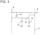
- Fig. 1 is a schematic drawing of an organic electroluminescent element having a sealing structure.
- a first embodiment of the organic electroluminescent element of the invention comprises a component layer comprising an light emission layer, the component layer containing at least one selected from a compound (hereinafter also referred to as the compound in the invention) represented by formula I1, 12, 13, above. It is preferred that the compound described above is contained in the light emission layer.
- a compound hereinafter also referred to as the compound in the invention
- Japanese Patent O.P.I. Publication Nos. 2000-21572 and 2002-8860 disclose a method which incorporates a linkage group in the center of the biaryl position of a carbazole derivative molecule.
- linkage groups disclosed in these patent documents have a structure of small steric hindrance, and therefore, the carbazole derivatives disclosed therein is likely to maintain planarity of the molecule. It has been found that incorporation of a linkage group inhibiting such molecular planarity, i.e., incorporation of a linkage group twisting the aryl groups in the biaryl portion, further improves characteristics of the derivative.
- the linkage group linking the two aryl groups in the compounds represented by formulae I1 through 13 above exhibits the same effects as above. It has been proved that an organic EL element, employing such carbazole derivatives, provides improved emission efficiency and emission life. This is considered to be due to the reason that the incorporation in carbazole derivatives of a linkage group with a substituent, i.e., a sterically bulky linkage group, improves characteristics of the carbazole derivatives, resulting in increase of stabilization effect.
- R i1 through R i16 independently represent a hydrogen atom or a substituent.
- substituents include an alkyl group (for example, a methyl group, an ethyl group, an isopropyl group, a t-butyl group or a trifluoromethyl group), a cycloalkyl group (for example, a cyclopentyl group or a cyclohexyl group), an aralkyl group (for example, a benzyl group or a 2-phenetyl group), an alkoxy group (for example, an ethoxy group, a isopropoxy group or a butoxy group), and a halogen atom (for example, a fluorine atom).
- an alkyl group for example, a methyl group, an ethyl group, an isopropyl group, a t-butyl group or a trifluoromethyl group
- a cycloalkyl group for example
- a hydrogen atom or an alkyl group is preferred, and in the alkyl group, a methyl group is most preferred.
- R 21 through R 32 independently represent a hydrogen atom or a substituent.
- substituents include a substituted or unsubstituted alkyl group (for example, a methyl group, an ethyl group, an isopropyl group, a hydroxyethyl group, a methoxymethyl group, a trifluoromethyl group, or a t-butyl group), a substituted or unsubstituted cycloalkyl group (for example, a cyclopentyl group or a cyclohexyl group), a substituted or unsubstituted aralkyl group (for example, a benzyl group or a 2-phenetyl group), a substituted or unsubstituted aryl group (for example, a phenyl group, a naphthyl group, p-tolyl group, p-chlorophenyl group or a mesity
- the bisphenol compound described below of 2.0 g and 5.0 g of dibromotriphophoryl were heated at 320 °C for 5 hours in a nitrogen atmosphere.
- the resulting reaction mixture was added with ethyl acetate and water, and the organic solution phase of the mixture was separated, and purified according to silica gel column chromatography to obtain 1.4 g of the dibromo compound described below.
- a hole blocking layer which is comprised of at least one selected from the group consisting of a styryl compound, a triazole derivative, a phenanthroline derivative, an oxadiazole derivative and a boron derivative, is provided between the light emission layer and the cathode.
- the hole blocking layer is formed from a compound which prevents holes injected from the hole transporting layer from flowing into the cathode and effectively transports electrons injected from the cathode to the light emission layer.
- Physical properties required for compounds constituting the hole blocking layer are high electron mobility, low hole mobility, and inonization potential higher than that of the light emission layer or band gap wider than that of the light emission layer.
- the hole blocking layer has a function which encloses electrons and holes within the light emission layer and increases emission efficiency.
- a compound represented by formula 5, 6, 7, or 8 is preferred.
- R a1 through R a3 , R b1 through R b4 , and R c1 and R c2 independently represent an alkyl group, an aryl group or a heterocyclic group, provided that they may have a substituent; and A ra and A rb independently represent an aryl group or a heterocyclic group.
- alkyl group and the aryl group are the same as those denoted in R 1 through R 4 above.
- the heterocyclic group include a pyrrolyl group, a pyridyl group, a furyl group or a thienyl group.
- exemplified compounds include exemplified compounds disclosed in Japanese Patent O.P.I. Publication Nos. 2003-31367 , 2003-31368 , and Japanese Patent Publication No. 2721441 .
- the organic EL element of the invention comprises a component layer including a light emission layer provided between an anode and a cathode.
- a layer other than the light emission layer include a hole injecting layer, a hole transporting layer, a hole blocking layer, an electron transporting layer, an electron injecting layer.
- preferred examples of the organic EL element will be shown below, but the present invention is not limited thereto.
- a metal, an alloy, or an electroconductive compound each having a high working function (not less than 4 eV), and mixture thereof are preferably used as the electrode material.
- an electrode material include a metal such as Au, and a transparent electroconductive material such as CuI, indium tin oxide (ITO), SnO 2 , or ZnO, and a material capable of forming an amorphous and transparent conductive layer such as IDIXO (In 2 O 3 -ZnO).
- the anode may be prepared by forming a thin layer of the electrode material according to a depositing or spattering method, and by forming the layer into a desired pattern according to a photolithographic method.
- the pattern may be formed by depositing or spattering of the electrode material through a mask having a desired form.
- the transmittance of the anode is preferably 10% or more, and the sheet resistance of the anode is preferably not more than several hundred ⁇ / ⁇ .
- the thickness of the layer is ordinarily within the range of from 10 nm to 1 ⁇ m, and preferably from 10 to 200 nm, although it may vary due to kinds of materials used.
- a metal also referred to as an electron injecting metal
- an alloy also referred to as an electron injecting metal
- an electroconductive compound each having a low working function not more than 4 eV
- a mixture thereof is used as the electrode material.
- an electrode material include sodium, sodium-potassium alloy, magnesium, lithium, a magnesium/copper mixture, a magnesium/silver mixture, a magnesium/aluminum mixture, magnesium/indium mixture, an aluminum/aluminum oxide (Al 2 O 3 ) mixture, indium, a lithium/aluminum mixture, and a rare-earth metal.
- a mixture of an electron injecting metal and a metal higher in the working function than that of the electron injecting metal such as the magnesium/silver mixture, magnesium/aluminum mixture, magnesium/indium mixture, aluminum/aluminum oxide (Al 2 O 3 ) mixture, lithium/aluminum mixture, or aluminum is suitable from the view point of the electron injecting ability and resistance to oxidation.
- the cathode can be prepared forming a thin layer of such an electrode material by a method such as a deposition or spattering method.
- the sheet resistance as the cathode is preferably not more than several hundred ⁇ / ⁇ , and the thickness of the layer is ordinarily from 10 nm to 1 ⁇ m, and preferably from 50 to 200 nm. It is preferable in increasing the light emission efficiency that either the anode or the cathode of the organic EL element is transparent or semitransparent.
- the injecting layer is optionally provided, for example, an electron injecting layer or a hole injecting layer, and may be provided between the anode and the light emission layer or hole transporting layer, and between the cathode and the light emission layer or electron transporting layer as described above.
- the injecting layer herein referred to is a layer provided between the electrode and an organic layer in order to reduce the driving voltage or to improve of light emission efficiency.
- the buffer layer there are a hole injecting layer (an anode buffer layer) and an electron injecting layer (a cathode buffer layer), which are described in " Electrode Material” page 123, Div. 2 Chapter 2 of "Organic EL element and its frontier of industrialization” (published by NTS Corporation, November 30, 1998 ) in detail.
- the anode buffer layer (hole injecting layer) is described in Japanese Patent O.P.I. Publication Nos. 9-45479 , 9-260062 , and 8-288069 etc., and its examples include a phthalocyanine buffer layer represented by a copper phthalocyanine layer, an oxide buffer layer represented by a vanadium oxide layer, an amorphous carbon buffer layer, a polymer buffer layer employing an electroconductive polymer such as polyaniline (emeraldine), and polythiophene, etc.
- the cathode buffer layer (electron injecting layer) is described in Japanese Patent O.P.I. Publication Nos. 6-325871 , 9-17574 , and 9-74586 , etc. in detail, and its examples include a metal buffer layer represented by a strontium or aluminum layer, an alkali metal compound buffer layer represented by a lithium fluoride layer, an alkali earth metal compound buffer layer represented by a magnesium fluoride layer, and an oxide buffer layer represented by an aluminum oxide.
- the buffer layer (injecting layer) is preferably very thin and has a thickness of preferably from 0.1 to 100 nm depending on kinds of the material used.
- the blocking layer is a layer provided if necessary in addition to the fundamental configuration layers as described above, and is for example a hole blocking layer as described in Japanese Patent O.P.I. Publication Nos. 11-204258 , and 11-204359 , and on page 237 of "Organic EL element and its frontier of industrialization” (published by NTS Corporation, November 30, 1998 ).
- the hole blocking layer is an electron transporting layer in a broad sense, and is comprised of material having an ability of transporting electrons but an extremely poor ability of holes, which can increase a recombination probability of electrons and holes by transporting electrons and blocking holes.
- the electron blocking layer is an hole transporting layer in a broad sense, and is comprised of material having an ability of transporting holes but an extremely poor ability of electrons, which can increase a recombination probability of electrons and holes by transporting holes and blocking electrons.
- the hole transporting layer is comprised of material having an ability of transporting holes, and a hole injecting layer and an electron blocking layer are included in the hole transporting layer in a broad sense.
- the hole transporting layer or electron transporting layer may be a single layer or plural layers.
- a host contained in the light emission layer, a hole transporting material contained in the hole transporting layer adjacent to the light emission layer, and an electron transporting material contained in the electron transporting layer adjacent to the light emission layer be compounds having a maximum fluorescence wavelength of not longer than 415 nm.
- the light emission layer in the invention is a layer where electrons and holes, injected from electrodes, an electron transporting layer or a hole transporting layer, are recombined to emit light.
- the portions where light emits may be portions in the light emission layer or portions at the interface between the light emission layer and the layer adjacent thereto.
- the light emission layer can be formed employing a known method such as a vacuum deposition method, a spin coat method, a casting method and an LB method.
- the thickness of the light emission layer is not specifically limited, but is ordinarily from 5 nm to 5 ⁇ m.
- the light emission layer may be composed of a single layer comprising one or two or more kinds of light emission materials, or of plural layers comprising the same composition or different composition. It is preferred in the invention that the light emission layer be composed of two or more kinds of light emission materials, and one of the light emission materials is the compound in the invention.
- the light emission layer can be formed by the method such as that described in Japanese Patent O.P.I. Publication No. 57-51781 , in which a light emission material is dissolved in a solvent together with a binder such as a resin, and the thus obtained solution is formed into a thin layer by a method such as a spin-coat method. Thickness of the emission layer thus formed is not specially restricted. Although the thickness of the layer thus formed is optionally selected, the thickness is ordinarily from 5 nm to 5 ⁇ m.
- the main compound is called a host, and another a dopant.
- the compound represented by formulae J1, J2 is preferably used as a host.
- the dopant content is from 0.1% to less than 15% by weight based on the host content.
- the compound having the highest content (by weight) in the mixture is a host compound (also referred to as simply a host) and the compound other than the host compound is a dopant compound (also referred to as simply a dopant).
- a host compound also referred to as simply a host
- a dopant compound also referred to as simply a dopant
- compound A:compound B:compound C in the light emission layer is 5:10:85
- compounds A and B are dopant compounds
- compound C is a host compound.
- the host compound in the light emission layer is preferably an organic compound or a complex.
- the host compound has a wavelength providing phosphorescence maximum of preferably no longer than 460 nm, which enables a visible light emission, particularly a BGR light emission.
- the host compound, having a phosphorescence maximum wavelength of no longer than 450 nm, has a wide energy gap (ionization potential-electron affinity), and advantageously works in the carrier trap type.
- the host compound is preferably a compound with high Tg (glass transition temperature
- the dopant is divided in two types in principle, one is an energy transfer type in which recombination of a carrier occurs on the host to which the carrier is transported to excite the host, the resulting energy is transferred to the dopant, and light is emitted from the dopant, and the other is a carrier trap type in which recombination of a carrier occurs on the dopant, a carrier trap material, and light is emitted from the dopant.
- energy level of the dopant in excited state is lower than that of the host in excited state.
- a phosphorescent compound is preferably used as a dopant.
- the phosphorescent compound in the invention is a compound which can emit light from the excited triplet, and has a phosphorescent quantum yield at 25 °C of not less than 0.001.
- the phosphorescent quantum yield at 25 °C is preferably not less than 0.01, and more preferably not less than 0.1.
- the phosphorescent quantum yield can be measured according to a method described in the fourth edition " Jikken Kagaku Koza 7", Bunko II, page 398 (1992) published by Maruzen .
- the phosphorescent quantum yield can be measured in a solution employing various kinds of solvents.
- the phosphorescent compound used in the invention may be any as long as it is a compound, in which the phosphorescent quantum yield measured employing any one of the solvents falls within the above-described range.
- the phosphorescent compound used as the dopant in the invention is preferably a metal complex compound containing a metal belonging to a group VIII of the periodic table as a center metal, and is more preferably an iridium compound, an osmium compound, a rhodium compound, a palladium compound or a platinum compound (a platinum complex), still more preferably an iridium compound, a rhodium compound, or a platinum compound, and most preferably an iridium compound.
- Examples of the phosphorescent compound include compounds disclosed in the following patent documents: WO00/70655 , Japanese Patent O.P.I. Publication Nos. 2002-280178 , 2001-181616 , 2002-280179 , 2001-181617 , 2002-280180 , 2001-247859 , 2002-299060 , 2001-313178 , 2002-302671 , 2001-345183 , and 2002-324679 , WO02/15645 , Japanese Patent O.P.I. Publication Nos. 2002-332291 , 2002-50484 , 2002-332292 , 2002-83684 , Japanese Patent Publication No.
- Examples of the phosphorescent compound used in the invention will be listed below, but the invention is not limited thereto. These compounds can be synthesized according to a method described in Inorg. Chem., 40, 1704-1711 .
- a fluorescent dopant may be added to the light emission layer besides the phosphorescent compound.
- the fluorescent compound include a coumarine dye, a pyrane die, a cyanine dye, a chloconium dye, a squalenium dye, an oxobenzanthracene dye, a fluorescene dye, a rhodamine dye, a pyrylium dye, a perylene dye, a stilbene dye, and a polythiophene dye, a rare earth element complex phosphorescent compound, and other known phosphorescent compounds.
- the hole transporting layer is comprised of material having an ability of transporting holes, and a hole injecting layer and an electron blocking layer are included in the hole transporting layer in a broad sense.
- the hole transporting layer or electron transporting layer may be a single layer or plural layers.
- the hole transporting materials are not specifically limited, and can be optionally selected from those employed for hole transporting materials in conventional photoconductive elements or known materials used in the hole injecting layer or hole transporting layer of conventional EL elements.
- the hole transporting material described above may be either an organic substance or an inorganic substance as long as it has a hole injecting ability, a hole transporting ability or an ability to form a barrier to electrons.
- the hole injecting material or the hole transporting material include a triazole derivative, an oxadiazole derivative, an imidazole derivative, a polyarylalkane derivative, a pyrazoline derivative and a pyrazolone derivative, a phenylenediamine derivative, an arylamine derivative, an amino substituted chalcone derivative, an oxazole derivative, a styryl anthracene derivative, a fluorenone derivative, a hydrazone derivative, a stilbene derivative, a silazane derivative, an aniline copolymer, and an electroconductive oligomer, particularly a thiophene oligomer.
- hole transporting material those described above are used, but a porphyrin compound, an aromatic tertiary amine compound, or a styrylamine compound is preferably used, and an aromatic tertiary amine compound is more preferably used.
- aromatic tertiary amine compound and styrylamine compound include N,N,N',N'-tetraphenyl-4,4'-diaminophenyl, N,N'-diphenyl-N,N'-bis(3-methylphenyl)-[1,1'-biphenyl]-4,4'-diamine (TPD), 2,2'-bis(4-di-p-tolylaminophenyl)propane, 1,1'-bis(4-di-p-tolylaminophenyl)cyclohexane, N,N,N',N'-tetra-p-tolyl-4,4'-diaminobiphenyl, 1,1'-bis(4-di-p-tolylaminophenyl)-4-phenylcyclohexane, bis(4-dimethylamino-2-methylphenyl)-phenylmethane, bis(4-di-
- 5,061,569 which have two condensed aromatic rings in the molecule thereof such as 4,4'-bis[N-(1-naphthyl)-N-phenylamino]biphenyl (NPD), and compounds described in Japanese Patent O.P.I. Publication No. 4-308688 such as 4,4',4''-tris[N-(3-methylphenyl)-N-phenylamino]-triphenylamine (MTDATA) in which three triphenylamine units are bonded in a starburst form.
- NPD 4,4'-bis[N-(1-naphthyl)-N-phenylamino]biphenyl
- MTDATA 4,4',4''-tris[N-(3-methylphenyl)-N-phenylamino]-triphenylamine
- a polymer in which the material mentioned above is introduced in the polymer chain or a polymer having the material as the polymer main chain can be also used.
- inorganic compounds such as p-Si and p-SiC are usable.
- the hole transporting material contained in the hole transporting layer is preferably a compound having a maximum fluorescence wavelength of not longer than 415 nm. That is, the hole transporting material is preferably a material with high Tg, which has a hole transporting ability, and prevents the emission wavelength from shifting to longer wavelength.
- the hole transporting layer can be formed by layering the hole transporting material by a known method such as a vacuum deposition method, a spin coat method, a casting method, an ink jet method, and an LB method.
- the thickness of the hole transporting layer is not specifically limited, but is ordinarily from 5 to 5000 nm.
- the hole transporting layer may be composed of a single layer structure comprising one or two or more of the materials mentioned above.
- the electron transporting layer comprises a material (an electron transporting material) having an electron transporting ability, and in a broad sense refers to an electron injecting layer or a hole blocking layer.
- the electron transporting layer can be provided as a single layer or plural layers.
- an electron transporting material (which serves also as a hole blocking material) used in a single electron transporting layer or in the electron transporting layer closest to the cathode of plural electron transporting layers, compounds to be described below are known.
- the electron transporting layer may be any layer, as long as it has a function of incorporating electrons injected from a cathode to a light emission layer, and a material used in the electron transporting layer can be optionally selected from known compounds used as electron transporting materials.
- Examples of the material used in the electron transporting layer include a nitro-substituted fluorene derivative, a diphenylquinone derivative, a thiopyran dioxide derivative, a carbodiimide, a fluolenylidenemethane derivative, an anthraquinodimethane, an anthrone derivative, and an oxadiazole derivative.
- thiadiazole derivative which is formed by substituting the oxygen atom in the oxadiazole ring of the foregoing oxadiazole derivative with a sulfur atom
- a quinoxaline derivative having a quinoxaline ring known as an electron withdrawing group are usable as the electron transporting material.
- a polymer in which the material mentioned above is introduced in the polymer side chain or a polymer having the material as the polymer main chain can be also used.
- a metal complex of an 8-quinolynol derivative such as aluminum tris-(8-quinolynol) (Alq 3 ), aluminum tris-(5,7-dichloro-8-quinolynol), aluminum tris-(5,7-dibromo-8-quinolynol), aluminum tris-(2-methyl-8-quinolynol), aluminum tris-(5-methyl-8-quinolynol), or zinc bis-(8-quinolynol) (Znq 2 ), and a metal complex formed by replacing the central metal of the foregoing complexes with another metal atom such as In, Mg, Cu, Ca, Sn, Ga or Pb, can be used as the electron transporting material.
- another metal atom such as In, Mg, Cu, Ca, Sn, Ga or Pb
- a metal free or metal-containing phthalocyanine, and a derivative thereof, in which the molecular terminal is replaced by a substituent such as an alkyl group or a sulfonic acid group are also preferably used as the electron transporting material.
- the distyrylpyrazine derivative exemplified as a material for the light emission layer may preferably be employed as the electron transporting material.
- An inorganic semiconductor such as n-Si and n-SiC may also be used as the electron transporting material in a similar way as in the hole transporting layer.
- a material used in the electron transporting layer is preferably a compound having a maximum fluorescence wavelength of not longer than 415 nm. That is, the material used in the electron transporting layer is preferably a material with high Tg, which has an electron transporting ability, and prevents the emission wavelength from shifting to longer wavelength.
- the electron transporting layer can be formed by layering the electron transporting material by a known method such as a vacuum deposition method, a spin coat method, a casting method, an ink jet method, an LB method, a transfer method, or a printing method.
- the thickness of the electron transporting layer is not specifically limited, but is ordinarily from 5 to 5000 nm.
- the electron transporting layer may be composed of a single layer structure comprising one or two or more of the materials mentioned above.
- Examples of a substrate preferably employed for the organic electroluminescence element in the invention include glass, quartz and plastic. Especially preferred one is a resin film capable of providing flexibility to the organic EL element. When light is taken out from the substrate side, the substrate is transparent or translucent.
- the resin film is not specifically limited, and examples of the resin film include films of polyesters such as polyethylene terephthalate and polyethylene naphthalate; polyethylene; polypropylene; cellophane; cellulose esters such as cellulose diacetate, cellulose triacetate, cellulose acetate butyrate, cellulose acetate propionate, cellulose acetate phthalate, and cellulose nitrate or their derivatives; polyvinylidene chloride; polyvinyl alcohol; polyethylene vinyl alcohol; syndiotactic polystyrene; polycarbonate; norbornene resin; polymethylpentene; polyether ketone; polyimide; polyether sulfone; polysulfone; polyether ketone imide; polyamide; fluorine-contained resin; nylon; polymethyl methacrylate; polyacrylate or polyarylate; norbornene resin (or cyclolefin resin) such as ARTON (produced by JSR Co., Ltd.) or APER (produced by Mit
- the surface of the resin film may be covered with a cover layer of an inorganic or organic compound or a hybrid cover layer comprised of both compounds.
- the cover layer include a silica layer according to a sol-gel method, organic layers formed according to coating of polymers (including layers obtained by subjecting a layer containing a polymerizable organic compound to post-treatment such as UV irradiation or heating), a DLC layer, and a metal oxide or metal nitride layer.
- Examples of the metal oxide or metal nitride constituting the metal oxide or metal nitride layer include a metal oxide such as silicon oxide, titanium oxide, or aluminum oxide, a metal nitride such as silicon nitride, and a metal nitride oxide such as silicon nitride oxide or titanium nitride oxide.
- the resin film whose surface is covered with a cover layer of an inorganic or organic compound or a hybrid cover layer comprised of both compounds, is preferably a film with high barrier having a water vapor transmittance of not more than 0.01 g/m 2 ⁇ day ⁇ atmospheric pressure plasma discharge treatment apparatus.
- the preparation of the organic EL element which has the constitution, Anode/Hole injecting layer/Hole transporting layer/Light emission layer/Electron transporting layer/Electron injecting layer/Cathode, will be described.
- a thin layer of a desired material for an electrode such as a material of the anode is formed on a suitable substrate by a deposition or sputtering method to prepare the anode, so that the thickness of the layer is not more than 1 ⁇ m, and preferably within the range of from 10 to 200 nm.
- the hole injecting layer, the hole transporting layer, the light emission layer, the electron transporting layer and the electron injecting layer, which constitute the element are formed on the resulting anode in that order as organic compound thin layers.
- a spin coating method As methods for formation of the thin layers, there are a spin coating method, a casting method, an ink jet method, a vacuum deposition method, and a printing method, however, a spin coating method and a vacuum deposition method are preferably used, since a uniform layer can be formed and a pinhole is formed with difficulty. Different methods may be used for formation of different layers.
- vacuum deposition is preferably carried out at a boat temperature of from 50° C to 450° C, at a degree of vacuum of from 10 -6 to 10 -2 Pa, at a deposition speed of from 0.01 to 50 nm/second, and at a substrate temperature of from -50 to 300° C to form a layer with a thickness of from 0.1 nm to 5 ⁇ m.
- a thin layer comprised of a material for a cathode is formed thereon to prepare a cathode, employing, for example, a deposition method or sputtering method to give a thickness of not more than 1 ⁇ m, and preferably from 50 to 200 nm.
- a desired organic EL element is obtained.
- the layers from the hole injecting layer to the cathode are continuously formed under one time of vacuuming to obtain an organic EL element.
- a different layer formation method may be inserted. When the different method is used, its process is required to be carried out under a dry inert gas atmosphere.
- the layer formation method is carried out preferably according to a deposition method, an ink jet method or a printing method.
- a deposition method is used as the layer formation method, patterning of the layer is preferably carried out employing a shadow mask.
- the organic EL element can be prepared in the reverse order, in which the cathode, the electron injecting layer, the electron transporting layer, the light emission layer, the hole transporting layer, the hole injecting layer, and the anode are formed in that order.
- Examples of the light emission sources include a home lamp, a room lamp in a car, a backlight for a watch or a liquid crystal, a light source for boarding advertisement, a signal device, a light source for a photo memory medium, a light source for an electrophotographic copier, a light source for an optical communication instrument, and a light source for an optical sensor, but are not limited thereto.
- the organic EL element of the invention may be an organic EL element having a resonator structure.
- the organic EL element having a resonator structure is applied to a light source for a photo-memory medium, a light source for an electrophotographic copier, a light source for an optical communication instrument, or a light source for a photo-sensor, but its application is not limited thereto.
- a laser oscillation may be carried out.
- a pattern was formed on a substrate (NA-45, manufactured by NH Technoglass Co., Ltd.) composed of a glass plate and a 150 nm ITO (indium tin oxide) layer as an anode. Then the resulting transparent substrate having the ITO transparent electrode was subjected to ultrasonic washing in i-propyl alcohol and dried by a dry nitrogen gas and subjected to UV-ozone cleaning for 5 minutes.
- a substrate NA-45, manufactured by NH Technoglass Co., Ltd.
- ITO indium tin oxide
- the thus obtained transparent substrate was fixed on a substrate holder of a vacuum deposition apparatus available on the market. Further, ⁇ -NPD, CBP, Ir-12, BCP and Alq 3 were put in each of five resistive heating molybdenum boats, and set in the vacuum deposition apparatus.
- BCP was deposited onto the resulting light emission layer to form a hole blocking layer with a thickness of 10 nm, and then, Alq 3 was deposited onto the resulting layer to form an electron transporting layer with a thickness of 40 nm.
- the vacuum tank was opened, and a stainless steel mask having a rectangular hole was placed on the electron injecting layer. Further, 3 g of magnesium were put in a resistive heating molybdenum boat and 0.5 g of silver were put in a tungsten basket for deposition. The resulting boat and basket were set in the vacuum tank. Pressure in the vacuum tank was reduced to 2 X 10 -4 Pa. Then, the boat carrying magnesium was heated by supplying an electric current so as to deposit magnesium at a deposition speed of from 1.5 to 2.0 nm/sec, and at this time, the basket carrying silver was simultaneously heated so as to deposit silver at a deposition speed of 0.1 nm/sec to form a cathode electrode (200 nm) composed of a mixture of magnesium and silver. Thus, a comparative organic EL element sample OLED 1-1 was prepared.
- Organic EL element samples OLED 1-2 through 1-9, 1-21, 1-22, 1-26 through 1-28 were prepared in the same manner as comparative organic EL element sample OLED 1-1, except that CBP used in the light emission layer was replaced with those (comparative compounds 1 through 10 or Exemplified compounds in the invention) as shown in Table 1.
- emission luminance L (cd/m 2 ) of light emitted and time ( ⁇ ) when the initial emission luminance after emission reduces by half (hereinafter also referred to as half life) were measured according to CS-1000 produced by Minolta Co., Ltd.
- Emission luminance and half life of the organic EL element samples OLED 1-2 through 1-9, 1-21, 1-22, 1-26 through 1-28 were expressed by a relative value when the emission luminance and half life of comparative organic EL element sample OLED 1-1 were set at 100, respectively.
- the results are shown in Table 1.
- Table 1 Sample OLED No. Compound used in light emission layer Emission luminance Half life Remarks 1-1 CBP 100 100 Comp. 1-2 Comparative compound 1 98 105 Comp. 1-3 Comparative compound 2 90 113 Comp. 1-4 Comparative compound 3 102 109 Comp. 1-5 Comparative compound 4 110 60 Comp. 1-6 Comparative compound 5 86 101 Comp. 1-7 Comparative compound 6 82 93 Comp. 1-8 Comparative compound 7 77 74 Comp.
- inventive organic EL element samples OLED 1-26 through 1-28 comprising the compound in the invention provide high emission luminance and long half life as compared with comparative organic EL element samples OLED 1-1 through 1-9, 1-21 and 1-22.
- Organic EL element samples OLED, and 1-26G through 1-28G were prepared in the same manner as in Organic EL element samples OLED, respectively, except that Ir-1 was used instead of Ir-12, and the resulting samples exhibited the same results as above. Further, organic EL element samples OLED 1-26 R through 1-28 R were prepared in the same manner as in organic EL element samplesl-26 through 1-28, respectively, except that Ir-9 was used instead of Ir-12, and the resulting samples exhibited the same results as above. Green light was emitted from organic EL elements employing Ir-1, and red light was emitted from organic EL elements employing Ir-9.
- Organic EL element samples OLED 3-1 through 3-12 and 3-23 through 3-25 were prepared in the same manner as comparative organic EL element sample OLED 1-1, except that the host compound used in the light emission layer and the compound used in the hole blocking layer were replaced with those as shown in Table 3, respectively.
- emission luminance and half life are expressed by a relative value when the emission luminance and luminance half life of organic EL element sample OLED 3-1 were set at 100, respectively.
- Table 3 Sample OLED No. Compound used in light emission layer Compound used in hole blocking layer Emission luminance (%) Half life (%) Remarks 3-1 Comparative compound 1 Compound A1 100 100 Comp. 3-2 Comparative compound 2 Compound A1 94 112 Comp. 3-3 Comparative compound 3 Compound A1 104 111 Comp. 3-4 Comparative compound 4 Compound A1 108 75 Comp. 3-5 Comparative compound 5 Compound A1 92 105 Comp. 3-6 Comparative compound 6 Compound A1 88 105 Comp. 3-7 Comparative compound 7 Compound A1 83 90 Comp.
- inventive organic EL element samples employing the compound in the invention in the light emission layer provide high emission luminance and long luminance half life as compared with comparative organic EL element samples employing the comparative compound in the light emission layer.
- inventive organic EL element samples employing BCP, Compound A1, OXD7, TAZ or B1 as a hole blocking material used in the hole blocking layer exhibited higher emission luminance and longer luminance life as compared to comparative organic EL element samples employing BCP, Compound A1, OXD7, TAZ or B1 as a hole blocking material in the hole blocking layer.
- the present invention can provide an organic electroluminescent element with high luminance, high emission efficiency, high durability.
Claims (7)
- Organisches elektrolumineszierendes Element mit einer Anode, einer Kathode und einer Komponentenschicht, welche eine Lichtemissionsschicht umfasst, wobei die Komponentenschicht zwischen der Anode und der Kathode angeordnet ist, wobei die Komponentenschicht eine Verbindung enthält, die durch die folgende Formel 11, 12 oder 13 dargestellt ist:


- Organisches elektrolumineszierendes Element gemäß Anspruch 1, wobei eine Lochsperrschicht zwischen der Lichtemissionsschicht und der Kathode vorgesehen ist.
- Organisches elektrolumineszierendes Element gemäß Anspruch 2, wobei die Lochsperrschicht aus zumindest einer Substanz besteht, die ausgewählt ist aus der Gruppe, die aus einer Styrylverbindung, einem Triazoldrivat, einem Phenanthrolinderivat, einem Oxadiazolderivat und einem Borderivat besteht.
- Organisches elektrolumineszierendes Element gemäß Anspruch 2, wobei die Lochsperrschicht aus zumindest einer Substanz besteht, die ausgewählt ist aus der Gruppe, die aus Verbindungen besteht, die durch die Formeln 5, 6, 7 oder 8 dargestellt sind:


- Organisches elektrolumineszierendes Element gemäß Anspruch 1, wobei die Lichtemissionsschicht die Verbindung enthält, die durch die obige Formel 11, 12 oder 13 dargestellt ist.
- Organisches elektrolumineszierendes Element gemäß irgendeinem der Ansprüche 1 bis 5, wobei das organische elektrolumineszierende Element eine phosphoreszierende Verbindung enthält.
- Organisches elektrolumineszierendes Element gemäß Anspruch 6, wobei die phosphoreszierende Verbindung ein Osmiumkomplex, ein Iridiumkomplex oder ein Platinkomplex ist.
Applications Claiming Priority (7)
| Application Number | Priority Date | Filing Date | Title |
|---|---|---|---|
| JP2002342193 | 2002-11-26 | ||
| JP2003061201 | 2003-03-07 | ||
| JP2003084073 | 2003-03-26 | ||
| JP2003084075 | 2003-03-26 | ||
| JP2003084071 | 2003-03-26 | ||
| JP2003160609A JP4356363B2 (ja) | 2002-11-26 | 2003-06-05 | 有機エレクトロルミネッセンス素子及びそれを有する表示装置 |
| EP03026685A EP1424381A3 (de) | 2002-11-26 | 2003-11-20 | Organisches Elektrolumineszenzelement und Anzeige- und Beleuchtungsvorrichtung |
Related Parent Applications (1)
| Application Number | Title | Priority Date | Filing Date |
|---|---|---|---|
| EP03026685A Division EP1424381A3 (de) | 2002-11-26 | 2003-11-20 | Organisches Elektrolumineszenzelement und Anzeige- und Beleuchtungsvorrichtung |
Publications (2)
| Publication Number | Publication Date |
|---|---|
| EP2765174A1 EP2765174A1 (de) | 2014-08-13 |
| EP2765174B1 true EP2765174B1 (de) | 2018-05-30 |
Family
ID=32303850
Family Applications (5)
| Application Number | Title | Priority Date | Filing Date |
|---|---|---|---|
| EP03026685A Withdrawn EP1424381A3 (de) | 2002-11-26 | 2003-11-20 | Organisches Elektrolumineszenzelement und Anzeige- und Beleuchtungsvorrichtung |
| EP14165973.0A Expired - Fee Related EP2765174B1 (de) | 2002-11-26 | 2003-11-20 | Organisches Elektrolumineszenzelement und Anzeige und Illuminator |
| EP14165938.3A Expired - Fee Related EP2759585B1 (de) | 2002-11-26 | 2003-11-20 | Organisches Elektrolumineszenzelement und Anzeige und Illuminator |
| EP14166004.3A Expired - Fee Related EP2762546B1 (de) | 2002-11-26 | 2003-11-20 | Organisches Elektrolumineszenzelement und Anzeige und Illuminator |
| EP10174005.8A Expired - Fee Related EP2248870B1 (de) | 2002-11-26 | 2003-11-20 | Organisches Elektrolumineszenzelement und Anzeige- und Beleuchtungsvorrichtung |
Family Applications Before (1)
| Application Number | Title | Priority Date | Filing Date |
|---|---|---|---|
| EP03026685A Withdrawn EP1424381A3 (de) | 2002-11-26 | 2003-11-20 | Organisches Elektrolumineszenzelement und Anzeige- und Beleuchtungsvorrichtung |
Family Applications After (3)
| Application Number | Title | Priority Date | Filing Date |
|---|---|---|---|
| EP14165938.3A Expired - Fee Related EP2759585B1 (de) | 2002-11-26 | 2003-11-20 | Organisches Elektrolumineszenzelement und Anzeige und Illuminator |
| EP14166004.3A Expired - Fee Related EP2762546B1 (de) | 2002-11-26 | 2003-11-20 | Organisches Elektrolumineszenzelement und Anzeige und Illuminator |
| EP10174005.8A Expired - Fee Related EP2248870B1 (de) | 2002-11-26 | 2003-11-20 | Organisches Elektrolumineszenzelement und Anzeige- und Beleuchtungsvorrichtung |
Country Status (2)
| Country | Link |
|---|---|
| US (1) | US7629060B2 (de) |
| EP (5) | EP1424381A3 (de) |
Families Citing this family (57)
| Publication number | Priority date | Publication date | Assignee | Title |
|---|---|---|---|---|
| JP4707082B2 (ja) * | 2002-11-26 | 2011-06-22 | コニカミノルタホールディングス株式会社 | 有機エレクトロルミネッセンス素子および表示装置 |
| US7795801B2 (en) * | 2003-09-30 | 2010-09-14 | Konica Minolta Holdings, Inc. | Organic electroluminescent element, illuminator, display and compound |
| US7011871B2 (en) * | 2004-02-20 | 2006-03-14 | E. I. Du Pont De Nemours And Company | Charge transport compounds and electronic devices made with such compounds |
| JPWO2005089027A1 (ja) * | 2004-03-17 | 2008-01-31 | 出光興産株式会社 | 有機エレクトロルミネッセンス素子用材料及びそれを用いた有機エレクトロルミネッセンス素子 |
| US7315042B2 (en) * | 2004-11-18 | 2008-01-01 | 3M Innovative Properties Company | Semiconductors containing trans-1,2-bis(acenyl)ethylene compounds |
| US20060105199A1 (en) * | 2004-11-18 | 2006-05-18 | 3M Innovative Properties Company | Electroluminescent devices containing trans-1,2-bis(acenyl)ethylene compounds |
| US20060204783A1 (en) * | 2005-03-10 | 2006-09-14 | Conley Scott R | Organic electroluminescent device |
| WO2006104221A1 (en) * | 2005-03-28 | 2006-10-05 | Semiconductor Energy Laboratory Co., Ltd. | Anthracene derivative, material for light emitting element, light emitting element, light emitting device, and electronic device |
| US20080166562A1 (en) * | 2005-04-20 | 2008-07-10 | Koninklijke Philips Electronics, N.V. | Matrix Material for Organic Electroluminescent Devices |
| GB2472525B (en) * | 2005-06-09 | 2011-07-13 | Konica Minolta Holdings Inc | Electroluminescent element, illuminator and display |
| JPWO2006132012A1 (ja) * | 2005-06-09 | 2009-01-08 | コニカミノルタホールディングス株式会社 | 有機エレクトロルミネッセンス素子、照明装置及び表示装置 |
| US7651791B2 (en) | 2005-12-15 | 2010-01-26 | Idemitsu Kosan Co., Ltd. | Material for organic electroluminescence device and electroluminescence device employing the same |
| US7977862B2 (en) * | 2005-12-21 | 2011-07-12 | Lg Display Co., Ltd. | Organic light emitting devices |
| KR102103062B1 (ko) | 2006-02-10 | 2020-04-22 | 유니버셜 디스플레이 코포레이션 | 시클로금속화 이미다조[1,2-f]페난트리딘 및 디이미다조[1,2-a:1',2'-c]퀴나졸린 리간드, 및 이의 등전자성 및 벤즈고리화된 유사체의 금속 착체 |
| US7731377B2 (en) * | 2006-03-21 | 2010-06-08 | Semiconductor Energy Laboratory Co., Ltd. | Backlight device and display device |
| EP2557138B1 (de) | 2006-03-23 | 2016-08-10 | Konica Minolta Holdings, Inc. | Organische Elektrolumineszenzvorrichtung, Anzeige und Beleuchtungsvorrichtung |
| CN101506163B (zh) * | 2006-08-30 | 2012-05-02 | 株式会社半导体能源研究所 | 合成蒽衍生物的方法和蒽衍生物、发光元件、发光装置、电子装置 |
| US7723722B2 (en) | 2007-03-23 | 2010-05-25 | Semiconductor Energy Laboratory Co., Ltd. | Organic compound, anthracene derivative, and light-emitting element, light-emitting device, and electronic device using anthracene derivative |
| CN110724124A (zh) | 2007-05-17 | 2020-01-24 | 株式会社半导体能源研究所 | 三唑衍生物 |
| US20080286445A1 (en) * | 2007-05-17 | 2008-11-20 | Semiconductor Energy Laboratory Co., Ltd. | Composition, and method of fabricating light-emitting element |
| WO2009081718A1 (en) * | 2007-12-21 | 2009-07-02 | Semiconductor Energy Laboratory Co., Ltd. | Triazole derivative, light-emitting element, light-emitting device, and electronic device |
| KR20090098589A (ko) * | 2008-03-14 | 2009-09-17 | 삼성전자주식회사 | 인데노 인덴계 화합물, 이를 이용한 유기 발광 소자 및 그제조 방법 |
| KR20110018376A (ko) * | 2008-06-23 | 2011-02-23 | 스미또모 가가꾸 가부시키가이샤 | 조성물 및 상기 조성물을 이용하여 이루어지는 발광 소자 |
| WO2010005066A1 (en) * | 2008-07-08 | 2010-01-14 | Semiconductor Energy Laboratory Co., Ltd. | Carbazole derivative, light-emitting element material, light-emitting element, and light-emitting device |
| KR101174090B1 (ko) | 2008-08-25 | 2012-08-14 | 제일모직주식회사 | 유기광전소자용 재료 및 이를 포함하는 유기광전소자 |
| KR101661328B1 (ko) * | 2008-09-19 | 2016-09-29 | 가부시키가이샤 한도오따이 에네루기 켄큐쇼 | 카르바졸 유도체 및 그 제조 방법 |
| JP5591822B2 (ja) * | 2008-12-12 | 2014-09-17 | イー・アイ・デュポン・ドウ・ヌムール・アンド・カンパニー | 光活性組成物、および、この組成物で形成された電子素子 |
| KR101288557B1 (ko) | 2008-12-24 | 2013-07-22 | 제일모직주식회사 | 신규한 유기광전소자용 화합물 및 이를 포함하는 유기광전소자 |
| CN102292327A (zh) * | 2009-01-22 | 2011-12-21 | 保土谷化学工业株式会社 | 具有连接有吡啶基的三唑环结构的化合物以及有机电致发光器件 |
| US20100295027A1 (en) * | 2009-05-22 | 2010-11-25 | Idemitsu Kosan Co., Ltd. | Organic electroluminescence device |
| KR20120052231A (ko) | 2009-10-16 | 2012-05-23 | 이데미쓰 고산 가부시키가이샤 | 함플루오렌 방향족 화합물, 유기 일렉트로루미네선스 소자용 재료 및 그것을 사용한 유기 일렉트로루미네선스 소자 |
| US8617720B2 (en) | 2009-12-21 | 2013-12-31 | E I Du Pont De Nemours And Company | Electroactive composition and electronic device made with the composition |
| US8288187B2 (en) | 2010-01-20 | 2012-10-16 | Universal Display Corporation | Electroluminescent devices for lighting applications |
| US8993125B2 (en) | 2010-05-21 | 2015-03-31 | Semiconductor Energy Laboratory Co., Ltd. | Triazole derivative, and light-emitting element, light-emitting device, electronic device and lighting device using the triazole derivative |
| WO2011161727A1 (ja) * | 2010-06-24 | 2011-12-29 | パナソニック株式会社 | 有機el素子の製造方法、表示装置、発光装置および紫外光照射装置 |
| JPWO2012121101A1 (ja) * | 2011-03-04 | 2014-07-17 | コニカミノルタ株式会社 | 有機エレクトロルミネッセンス素子 |
| CN107501244B (zh) | 2011-11-22 | 2022-05-03 | 出光兴产株式会社 | 芳香族杂环衍生物、有机电致发光元件用材料以及有机电致发光元件 |
| KR102012047B1 (ko) | 2012-01-06 | 2019-08-19 | 유니버셜 디스플레이 코포레이션 | 효율이 큰 인광 물질 |
| US9386657B2 (en) | 2012-03-15 | 2016-07-05 | Universal Display Corporation | Organic Electroluminescent materials and devices |
| US9540329B2 (en) | 2012-07-19 | 2017-01-10 | Universal Display Corporation | Organic electroluminescent materials and devices |
| KR102024117B1 (ko) * | 2012-09-17 | 2019-09-24 | 삼성디스플레이 주식회사 | 축합환 화합물 및 이를 포함한 유기 발광 소자 |
| US9252363B2 (en) | 2012-10-04 | 2016-02-02 | Universal Display Corporation | Aryloxyalkylcarboxylate solvent compositions for inkjet printing of organic layers |
| US9196860B2 (en) | 2012-12-04 | 2015-11-24 | Universal Display Corporation | Compounds for triplet-triplet annihilation upconversion |
| US8716484B1 (en) | 2012-12-05 | 2014-05-06 | Universal Display Corporation | Hole transporting materials with twisted aryl groups |
| US9653691B2 (en) | 2012-12-12 | 2017-05-16 | Universal Display Corporation | Phosphorescence-sensitizing fluorescence material system |
| JP6317544B2 (ja) * | 2013-02-15 | 2018-04-25 | 出光興産株式会社 | 有機エレクトロルミネッセンス素子および電子機器 |
| CN103193695B (zh) * | 2013-04-22 | 2015-08-05 | 中国药科大学 | 3-苯基-3-吡咯基戊烷类衍生物及其医药用途 |
| US9577198B1 (en) | 2013-08-01 | 2017-02-21 | Nitto Denko Corporation | 2,6-bis(diarylaminophenyl)benzene and derivatives thereof as hole-transport compounds in organic light-emitting devices |
| US9876173B2 (en) | 2013-12-09 | 2018-01-23 | Universal Display Corporation | Organic electroluminescent materials and devices |
| US9450198B2 (en) | 2014-04-15 | 2016-09-20 | Universal Display Corporation | Organic electroluminescent materials and devices |
| US9692003B2 (en) * | 2015-04-15 | 2017-06-27 | Feng-wen Yen | Phenanthroline derivative and use thereof |
| KR20170101128A (ko) | 2016-02-26 | 2017-09-05 | 가부시키가이샤 한도오따이 에네루기 켄큐쇼 | 유기 화합물, 발광 소자, 발광 장치, 전자 기기, 및 조명 장치 |
| KR20180113659A (ko) * | 2017-04-06 | 2018-10-17 | 삼성디스플레이 주식회사 | 발광 재료 및 이를 포함하는 유기 전계 발광 소자 |
| CN107501164B (zh) * | 2017-09-06 | 2020-04-21 | 山西大学 | 一种含四苯基乙烯结构的双咔唑化合物及其制备和应用 |
| CN109836369B (zh) * | 2017-11-27 | 2022-06-07 | 中国科学院大连化学物理研究所 | 一种螺茚类空穴传输小分子及其在钙钛矿太阳能电池的应用 |
| CN111892531B (zh) * | 2020-09-08 | 2021-10-01 | 长春海谱润斯科技股份有限公司 | 一种有机化合物及其有机电致发光器件 |
| CN113149889A (zh) * | 2021-02-26 | 2021-07-23 | 阜阳欣奕华材料科技有限公司 | 一种化合物与有机电致发光器件 |
Family Cites Families (132)
| Publication number | Priority date | Publication date | Assignee | Title |
|---|---|---|---|---|
| US4356429A (en) | 1980-07-17 | 1982-10-26 | Eastman Kodak Company | Organic electroluminescent cell |
| JP2814435B2 (ja) | 1987-03-02 | 1998-10-22 | イーストマン・コダック・カンパニー | 改良薄膜発光帯をもつ電場発光デバイス |
| JP2815472B2 (ja) | 1990-01-22 | 1998-10-27 | パイオニア株式会社 | 電界発光素子 |
| US5061569A (en) | 1990-07-26 | 1991-10-29 | Eastman Kodak Company | Electroluminescent device with organic electroluminescent medium |
| US5093698A (en) * | 1991-02-12 | 1992-03-03 | Kabushiki Kaisha Toshiba | Organic electroluminescent device |
| JP2721441B2 (ja) | 1991-02-27 | 1998-03-04 | 株式会社リコー | 電界発光素子 |
| JP3016896B2 (ja) | 1991-04-08 | 2000-03-06 | パイオニア株式会社 | 有機エレクトロルミネッセンス素子 |
| EP1056140B1 (de) | 1992-08-28 | 2005-07-06 | Idemitsu Kosan Company Limited | Ladungsinjektionszusatzmaterial |
| JPH06325871A (ja) | 1993-05-18 | 1994-11-25 | Mitsubishi Kasei Corp | 有機電界発光素子 |
| JP3332491B2 (ja) | 1993-08-27 | 2002-10-07 | 三洋電機株式会社 | 有機el素子 |
| JP3758694B2 (ja) | 1994-10-13 | 2006-03-22 | 三星エスディアイ株式会社 | 有機薄膜el素子 |
| JP3334408B2 (ja) | 1995-03-01 | 2002-10-15 | 三菱化学株式会社 | 有機電界発光素子及びその製造方法 |
| JP3561549B2 (ja) | 1995-04-07 | 2004-09-02 | 三洋電機株式会社 | 有機エレクトロルミネッセンス素子 |
| JP3529543B2 (ja) | 1995-04-27 | 2004-05-24 | パイオニア株式会社 | 有機エレクトロルミネッセンス素子 |
| US5719467A (en) | 1995-07-27 | 1998-02-17 | Hewlett-Packard Company | Organic electroluminescent device |
| JPH0974586A (ja) | 1995-09-05 | 1997-03-18 | Matsushita Electric Ind Co Ltd | 無線同期装置 |
| JP3645642B2 (ja) | 1996-03-25 | 2005-05-11 | Tdk株式会社 | 有機エレクトロルミネセンス素子 |
| JP3161360B2 (ja) | 1996-04-19 | 2001-04-25 | 東ソー株式会社 | アリールアミン類の製造方法 |
| JPH10168443A (ja) * | 1996-12-17 | 1998-06-23 | Sanyo Shinku Kogyo Kk | 有機発光素子の正孔または電子輸送層等に用いられるフェニルカルバゾール誘導体 |
| JPH10233284A (ja) | 1997-02-19 | 1998-09-02 | Oki Electric Ind Co Ltd | 有機el素子 |
| JPH10340786A (ja) * | 1997-06-09 | 1998-12-22 | Toyo Ink Mfg Co Ltd | 有機エレクトロルミネッセンス素子材料およびそれを使用した有機エレクトロルミネッセンス素子 |
| JP3856546B2 (ja) * | 1997-11-11 | 2006-12-13 | 三井化学株式会社 | 有機電界発光素子 |
| JP3852509B2 (ja) | 1998-01-09 | 2006-11-29 | ソニー株式会社 | 電界発光素子及びその製造方法 |
| JPH11204359A (ja) | 1998-01-14 | 1999-07-30 | Tokin Corp | 圧粉磁芯の製造方法と製造装置 |
| US6329084B1 (en) * | 1998-06-15 | 2001-12-11 | Toyo Ink Mfg. Co., Ltd. | Compound for organic electro-luminescence device and organic electro-luminescence device using the compound |
| JP4003299B2 (ja) | 1998-07-06 | 2007-11-07 | 三菱化学株式会社 | 有機電界発光素子 |
| WO2000003565A1 (en) * | 1998-07-10 | 2000-01-20 | Fed Corporation | Amorphous molecular materials for optoelectronic devices and process for producing the same |
| JP3924943B2 (ja) * | 1998-08-24 | 2007-06-06 | 東洋インキ製造株式会社 | 有機エレクトロルミネッセンス素子材料およびそれを使用した有機エレクトロルミネッセンス素子 |
| US6097147A (en) | 1998-09-14 | 2000-08-01 | The Trustees Of Princeton University | Structure for high efficiency electroluminescent device |
| GB9820805D0 (en) | 1998-09-25 | 1998-11-18 | Isis Innovation | Divalent lanthanide metal complexes |
| EP1666561A1 (de) * | 1998-12-28 | 2006-06-07 | Idemitsu Kosan Company Limited | Organisches elektrolumineszierendes Element |
| AU3908400A (en) | 1999-03-23 | 2000-10-09 | University Of Southern California | Cyclometallated metal complexes as phosphorescent dopants in organic leds |
| EP3321954A1 (de) | 1999-05-13 | 2018-05-16 | The Trustees of Princeton University | Organische lichtemittierende vorrichtungen mit hoher wirkung basierend auf der elektrophosphoreszenz |
| JP2001181617A (ja) | 1999-12-27 | 2001-07-03 | Fuji Photo Film Co Ltd | オルトメタル化白金錯体からなる発光素子材料および発光素子 |
| JP2001181616A (ja) | 1999-12-27 | 2001-07-03 | Fuji Photo Film Co Ltd | オルトメタル化パラジウム錯体からなる発光素子材料および発光素子 |
| JP3929690B2 (ja) | 1999-12-27 | 2007-06-13 | 富士フイルム株式会社 | オルトメタル化イリジウム錯体からなる発光素子材料、発光素子および新規イリジウム錯体 |
| JP3929689B2 (ja) | 2000-03-28 | 2007-06-13 | 富士フイルム株式会社 | 高効率赤色発光素子、イリジウム錯体から成る発光素子材料及び新規イリジウム錯体 |
| JP3929706B2 (ja) | 2000-02-10 | 2007-06-13 | 富士フイルム株式会社 | イリジウム錯体からなる発光素子材料及び発光素子 |
| JP4890669B2 (ja) | 2000-03-13 | 2012-03-07 | Tdk株式会社 | 有機el素子 |
| TW532048B (en) * | 2000-03-27 | 2003-05-11 | Idemitsu Kosan Co | Organic electroluminescence element |
| JP4037033B2 (ja) | 2000-03-31 | 2008-01-23 | パイオニア株式会社 | 有機エレクトロルミネッセンス素子 |
| JP2002008860A (ja) | 2000-04-18 | 2002-01-11 | Mitsubishi Chemicals Corp | 有機電界発光素子 |
| JP2002015871A (ja) | 2000-04-27 | 2002-01-18 | Toray Ind Inc | 発光素子 |
| JP2001313178A (ja) | 2000-04-28 | 2001-11-09 | Pioneer Electronic Corp | 有機エレクトロルミネッセンス素子 |
| JP2001313179A (ja) | 2000-05-01 | 2001-11-09 | Mitsubishi Chemicals Corp | 有機電界発光素子 |
| JP4382961B2 (ja) | 2000-05-02 | 2009-12-16 | 富士フイルム株式会社 | 発光素子 |
| JP4048521B2 (ja) | 2000-05-02 | 2008-02-20 | 富士フイルム株式会社 | 発光素子 |
| JP5062797B2 (ja) | 2000-05-22 | 2012-10-31 | 昭和電工株式会社 | 有機エレクトロルミネッセンス素子および発光材料 |
| JP4683766B2 (ja) | 2000-05-22 | 2011-05-18 | 株式会社半導体エネルギー研究所 | アクティブマトリクス型発光装置 |
| US6645645B1 (en) | 2000-05-30 | 2003-11-11 | The Trustees Of Princeton University | Phosphorescent organic light emitting devices |
| JP2002062824A (ja) | 2000-06-05 | 2002-02-28 | Semiconductor Energy Lab Co Ltd | 発光装置 |
| JP4290858B2 (ja) | 2000-06-12 | 2009-07-08 | 富士フイルム株式会社 | 有機電界発光素子 |
| JP2002083684A (ja) | 2000-06-23 | 2002-03-22 | Semiconductor Energy Lab Co Ltd | 発光装置 |
| JP2002083685A (ja) * | 2000-06-28 | 2002-03-22 | Matsushita Electric Ind Co Ltd | 有機電界発光素子 |
| JP4340401B2 (ja) | 2000-07-17 | 2009-10-07 | 富士フイルム株式会社 | 発光素子及びイリジウム錯体 |
| JP4712232B2 (ja) | 2000-07-17 | 2011-06-29 | 富士フイルム株式会社 | 発光素子及びアゾール化合物 |
| JP2002043056A (ja) | 2000-07-19 | 2002-02-08 | Canon Inc | 発光素子 |
| JP2002036350A (ja) | 2000-07-31 | 2002-02-05 | Aica Kogyo Co Ltd | 曲げ加工品とその加工方法 |
| CN102041001B (zh) | 2000-08-11 | 2014-10-22 | 普林斯顿大学理事会 | 有机金属化合物和发射转换有机电致磷光 |
| JP2002141173A (ja) | 2000-08-22 | 2002-05-17 | Semiconductor Energy Lab Co Ltd | 発光装置 |
| JP4344494B2 (ja) | 2000-08-24 | 2009-10-14 | 富士フイルム株式会社 | 発光素子及び新規重合体子 |
| JP4554047B2 (ja) | 2000-08-29 | 2010-09-29 | 株式会社半導体エネルギー研究所 | 発光装置 |
| JP4505162B2 (ja) | 2000-09-21 | 2010-07-21 | 富士フイルム株式会社 | 発光素子および新規レニウム錯体 |
| JP4067286B2 (ja) | 2000-09-21 | 2008-03-26 | 富士フイルム株式会社 | 発光素子及びイリジウム錯体 |
| JP4454130B2 (ja) | 2000-09-25 | 2010-04-21 | 京セラ株式会社 | 有機エレクトロルミネッセンス素子 |
| JP4154140B2 (ja) | 2000-09-26 | 2008-09-24 | キヤノン株式会社 | 金属配位化合物 |
| JP2002184582A (ja) | 2000-09-28 | 2002-06-28 | Semiconductor Energy Lab Co Ltd | 発光装置 |
| JP4026740B2 (ja) | 2000-09-29 | 2007-12-26 | 富士フイルム株式会社 | 有機発光素子材料及びそれを用いた有機発光素子 |
| US6893743B2 (en) * | 2000-10-04 | 2005-05-17 | Mitsubishi Chemical Corporation | Organic electroluminescent device |
| JP4092901B2 (ja) | 2000-10-30 | 2008-05-28 | 株式会社豊田中央研究所 | 有機電界発光素子 |
| JP4086498B2 (ja) | 2000-11-29 | 2008-05-14 | キヤノン株式会社 | 金属配位化合物、発光素子及び表示装置 |
| JP4086499B2 (ja) | 2000-11-29 | 2008-05-14 | キヤノン株式会社 | 金属配位化合物、発光素子及び表示装置 |
| JP3855675B2 (ja) | 2000-11-30 | 2006-12-13 | 三菱化学株式会社 | 有機電界発光素子 |
| JP4048525B2 (ja) | 2000-12-25 | 2008-02-20 | 富士フイルム株式会社 | 新規インドール誘導体およびそれを利用した発光素子 |
| JP2002255934A (ja) | 2000-12-25 | 2002-09-11 | Fuji Photo Film Co Ltd | 新規化合物、その重合体、それらを利用した発光素子材料およびその発光素子 |
| JP2002198170A (ja) | 2000-12-26 | 2002-07-12 | Nippon Seiki Co Ltd | 有機elパネル |
| JP3250561B1 (ja) | 2000-12-27 | 2002-01-28 | 株式会社デンソー | 有機el素子の製造方法 |
| JP2002203678A (ja) | 2000-12-27 | 2002-07-19 | Fuji Photo Film Co Ltd | 発光素子 |
| JP4677670B2 (ja) | 2000-12-27 | 2011-04-27 | 株式会社豊田中央研究所 | 有機電界発光素子の製造方法 |
| JP2002203679A (ja) | 2000-12-27 | 2002-07-19 | Fuji Photo Film Co Ltd | 発光素子 |
| JP4153694B2 (ja) | 2000-12-28 | 2008-09-24 | 株式会社東芝 | 有機el素子および表示装置 |
| US6720090B2 (en) | 2001-01-02 | 2004-04-13 | Eastman Kodak Company | Organic light emitting diode devices with improved luminance efficiency |
| JP3988915B2 (ja) | 2001-02-09 | 2007-10-10 | 富士フイルム株式会社 | 遷移金属錯体及びそれからなる発光素子用材料、並びに発光素子 |
| JP4598282B2 (ja) | 2001-02-09 | 2010-12-15 | 三井化学株式会社 | アミン化合物および該化合物を含有する有機電界発光素子 |
| JP4215145B2 (ja) | 2001-02-21 | 2009-01-28 | 富士フイルム株式会社 | 発光素子用材料及び発光素子 |
| JP4307000B2 (ja) | 2001-03-08 | 2009-08-05 | キヤノン株式会社 | 金属配位化合物、電界発光素子及び表示装置 |
| TWI243197B (en) | 2001-03-08 | 2005-11-11 | Univ Hong Kong | Organometallic light-emitting material |
| JP4438042B2 (ja) | 2001-03-08 | 2010-03-24 | キヤノン株式会社 | 金属配位化合物、電界発光素子及び表示装置 |
| JP2002334787A (ja) | 2001-03-09 | 2002-11-22 | Sony Corp | 有機電界発光素子 |
| JP4655410B2 (ja) | 2001-03-09 | 2011-03-23 | ソニー株式会社 | 有機電界発光素子 |
| JP2002334786A (ja) | 2001-03-09 | 2002-11-22 | Sony Corp | 有機電界発光素子 |
| JP2002334788A (ja) | 2001-03-09 | 2002-11-22 | Sony Corp | 有機電界発光素子 |
| JP2002343572A (ja) | 2001-03-14 | 2002-11-29 | Canon Inc | ポルフィリン誘導体化合物を用いた発光素子および表示装置 |
| JP4307001B2 (ja) | 2001-03-14 | 2009-08-05 | キヤノン株式会社 | 金属配位化合物、電界発光素子及び表示装置 |
| JP2002280180A (ja) | 2001-03-16 | 2002-09-27 | Canon Inc | 有機発光素子 |
| JP2002280178A (ja) | 2001-03-16 | 2002-09-27 | Canon Inc | 有機発光素子 |
| JP4169246B2 (ja) | 2001-03-16 | 2008-10-22 | 富士フイルム株式会社 | ヘテロ環化合物及びそれを用いた発光素子 |
| JP2002280179A (ja) | 2001-03-16 | 2002-09-27 | Canon Inc | 有機発光素子 |
| JP3964245B2 (ja) | 2001-03-28 | 2007-08-22 | 株式会社半導体エネルギー研究所 | 有機発光素子および前記素子を用いた発光装置 |
| JP2002299060A (ja) | 2001-03-30 | 2002-10-11 | Fuji Photo Film Co Ltd | 有機発光素子 |
| JP4972844B2 (ja) | 2001-03-30 | 2012-07-11 | コニカミノルタホールディングス株式会社 | 有機エレクトロルミネッセンス素子 |
| JP2002363227A (ja) | 2001-04-03 | 2002-12-18 | Fuji Photo Film Co Ltd | 新規ポリマーおよびそれを用いた発光素子 |
| JP2002302516A (ja) | 2001-04-03 | 2002-10-18 | Fuji Photo Film Co Ltd | 新規ポリマーおよびそれを用いた発光素子 |
| JP2002305083A (ja) | 2001-04-04 | 2002-10-18 | Mitsubishi Chemicals Corp | 有機電界発光素子 |
| JP2002308855A (ja) | 2001-04-05 | 2002-10-23 | Fuji Photo Film Co Ltd | 新規化合物、およびそれを用いた発光素子 |
| JP2002308837A (ja) | 2001-04-05 | 2002-10-23 | Fuji Photo Film Co Ltd | 新規化合物、およびそれを用いた発光素子 |
| JP2003007471A (ja) | 2001-04-13 | 2003-01-10 | Semiconductor Energy Lab Co Ltd | 有機発光素子および前記素子を用いた発光装置 |
| JP2002313559A (ja) | 2001-04-17 | 2002-10-25 | Canon Inc | 電荷注入型発光素子及びその製造方法 |
| JP2002324679A (ja) | 2001-04-26 | 2002-11-08 | Honda Motor Co Ltd | 有機エレクトロルミネッセンス素子 |
| US6998487B2 (en) * | 2001-04-27 | 2006-02-14 | Lg Chem, Ltd. | Double-spiro organic compounds and organic electroluminescent devices using the same |
| JP2002343568A (ja) | 2001-05-10 | 2002-11-29 | Sony Corp | 有機電界発光素子 |
| JP2002352957A (ja) | 2001-05-23 | 2002-12-06 | Honda Motor Co Ltd | 有機エレクトロルミネッセンス素子 |
| JP2002352961A (ja) | 2001-05-25 | 2002-12-06 | Toray Ind Inc | 有機電界発光装置 |
| JP2002352960A (ja) | 2001-05-29 | 2002-12-06 | Hitachi Ltd | 薄膜電界発光素子 |
| JP2002367771A (ja) | 2001-06-05 | 2002-12-20 | Toray Ind Inc | 有機電界発光素子 |
| JP2003007469A (ja) | 2001-06-25 | 2003-01-10 | Canon Inc | 発光素子及び表示装置 |
| JP4628594B2 (ja) | 2001-06-25 | 2011-02-09 | 昭和電工株式会社 | 有機発光素子および発光材料 |
| JP4789359B2 (ja) | 2001-07-11 | 2011-10-12 | 株式会社半導体エネルギー研究所 | 発光装置 |
| JP4003824B2 (ja) | 2001-07-11 | 2007-11-07 | 富士フイルム株式会社 | 発光素子 |
| JP4804662B2 (ja) | 2001-07-11 | 2011-11-02 | コニカミノルタホールディングス株式会社 | 有機エレクトロルミネッセンス素子及び表示装置 |
| JP4804661B2 (ja) | 2001-07-11 | 2011-11-02 | コニカミノルタホールディングス株式会社 | 有機エレクトロルミネッセンス素子 |
| JP4220696B2 (ja) * | 2001-10-16 | 2009-02-04 | 三井化学株式会社 | 炭化水素化合物、有機電界発光素子用材料および有機電界発光素子 |
| WO2003080760A1 (fr) * | 2002-03-22 | 2003-10-02 | Idemitsu Kosan Co., Ltd. | Materiau pour dispositifs electroluminescents organiques et dispositifs electroluminescents organiques produits avec ce materiau |
| EP2192632B1 (de) * | 2002-04-12 | 2014-09-03 | Konica Corporation | Organisches lichtemittierendes Element |
| US20030205696A1 (en) * | 2002-04-25 | 2003-11-06 | Canon Kabushiki Kaisha | Carbazole-based materials for guest-host electroluminescent systems |
| JP4256626B2 (ja) * | 2002-05-15 | 2009-04-22 | 富士フイルム株式会社 | ヘテロ環化合物及びそれを用いた発光素子 |
| JP4288895B2 (ja) | 2002-06-04 | 2009-07-01 | コニカミノルタホールディングス株式会社 | 有機エレクトロルミネッセンスの製造方法 |
| GB2408979B (en) * | 2002-09-10 | 2006-03-08 | Sankio Chemical Co Ltd | New process for producing arylamines |
| JP4707082B2 (ja) * | 2002-11-26 | 2011-06-22 | コニカミノルタホールディングス株式会社 | 有機エレクトロルミネッセンス素子および表示装置 |
| JP4158562B2 (ja) * | 2003-03-12 | 2008-10-01 | コニカミノルタホールディングス株式会社 | 有機エレクトロルミネッセンス素子及び表示装置 |
| JP2004311411A (ja) * | 2003-03-26 | 2004-11-04 | Konica Minolta Holdings Inc | 有機エレクトロルミネッセンス素子、照明装置および表示装置 |
| EP1464691B1 (de) * | 2003-03-26 | 2013-10-02 | Konica Minolta Holdings, Inc. | Organische elektrolumineszente Vorrichtung, Beleuchtungsvorrichtung und Anzeigevorrichtung |
-
2003
- 2003-11-20 US US10/718,025 patent/US7629060B2/en active Active
- 2003-11-20 EP EP03026685A patent/EP1424381A3/de not_active Withdrawn
- 2003-11-20 EP EP14165973.0A patent/EP2765174B1/de not_active Expired - Fee Related
- 2003-11-20 EP EP14165938.3A patent/EP2759585B1/de not_active Expired - Fee Related
- 2003-11-20 EP EP14166004.3A patent/EP2762546B1/de not_active Expired - Fee Related
- 2003-11-20 EP EP10174005.8A patent/EP2248870B1/de not_active Expired - Fee Related
Non-Patent Citations (1)
| Title |
|---|
| None * |
Also Published As
| Publication number | Publication date |
|---|---|
| EP2248870A2 (de) | 2010-11-10 |
| EP1424381A3 (de) | 2005-01-19 |
| EP2759585B1 (de) | 2018-08-15 |
| EP2759585A1 (de) | 2014-07-30 |
| EP2248870A3 (de) | 2011-02-02 |
| EP2248870B1 (de) | 2018-12-26 |
| EP2762546B1 (de) | 2018-06-06 |
| EP2765174A1 (de) | 2014-08-13 |
| EP1424381A2 (de) | 2004-06-02 |
| EP2762546A1 (de) | 2014-08-06 |
| US20040115476A1 (en) | 2004-06-17 |
| US7629060B2 (en) | 2009-12-08 |
Similar Documents
| Publication | Publication Date | Title |
|---|---|---|
| EP2765174B1 (de) | Organisches Elektrolumineszenzelement und Anzeige und Illuminator | |
| US6750608B2 (en) | Organic electroluminescence element and display | |
| US6835473B2 (en) | Organic electroluminescence element and display | |
| JP3925265B2 (ja) | 有機エレクトロルミネッセンス素子及びそれを用いた表示装置 | |
| JP4103491B2 (ja) | 有機エレクトロルミネッセンス素子及び表示装置 | |
| JP4427947B2 (ja) | 有機エレクトロルミネッセンス素子及び表示装置 | |
| EP1353388B1 (de) | Organisches lichtemittierendes Element | |
| JP4103492B2 (ja) | 有機エレクトロルミネッセンス素子および表示装置 | |
| JP4899284B2 (ja) | 有機エレクトロルミネッセンス素子、照明装置及び表示装置 | |
| EP1653784B1 (de) | Organisches elektrolumineszenz-bauelement, beleuchtungseinrichtung und display | |
| JP4103493B2 (ja) | 有機エレクトロルミネッセンス素子および表示装置 | |
| JPWO2005097940A1 (ja) | 有機エレクトロルミネッセンス素子材料、有機エレクトロルミネッセンス素子、表示装置及び照明装置 | |
| JP2004031004A (ja) | 有機エレクトロルミネッセンス素子及び表示装置 | |
| EP1267428B1 (de) | Organische elektrolumineszente Vorrichtung und vollfarbene Anzeigevorrichtung | |
| JP4254211B2 (ja) | 有機エレクトロルミネッセンス素子及び表示装置 | |
| US7759855B2 (en) | Organic electroluminescent element and display employing the same | |
| JP4356363B2 (ja) | 有機エレクトロルミネッセンス素子及びそれを有する表示装置 | |
| JP4374842B2 (ja) | 有機エレクトロルミネッセンス素子及び表示装置 | |
| JP4045932B2 (ja) | 有機エレクトロルミネッセンス素子及び表示装置 | |
| JP4265215B2 (ja) | 有機エレクトロルミネッセンス素子及び表示装置 | |
| JP3997937B2 (ja) | 有機エレクトロルミネッセンス素子、表示装置及び照明装置 | |
| JP4078960B2 (ja) | 有機エレクトロルミネッセンス素子及びその表示装置 | |
| JP4457529B2 (ja) | 有機エレクトロルミネッセンス素子 | |
| JP5104816B2 (ja) | 有機エレクトロルミネッセンス素子及びそれを有する表示装置 | |
| JP2012028823A (ja) | 有機エレクトロルミネッセンス素子 |
Legal Events
| Date | Code | Title | Description |
|---|---|---|---|
| PUAI | Public reference made under article 153(3) epc to a published international application that has entered the european phase |
Free format text: ORIGINAL CODE: 0009012 |
|
| 17P | Request for examination filed |
Effective date: 20140425 |
|
| AC | Divisional application: reference to earlier application |
Ref document number: 1424381 Country of ref document: EP Kind code of ref document: P |
|
| AK | Designated contracting states |
Kind code of ref document: A1 Designated state(s): DE GB |
|
| RIN1 | Information on inventor provided before grant (corrected) |
Inventor name: KINOSHITA, MOTOI Inventor name: SUZURI, YOSHIYUKI Inventor name: FUKUDA, MITSUHIRO Inventor name: KITA, HIROSHI Inventor name: YAMADA, TAKETOSHI Inventor name: UEDA, NORIKO Inventor name: OSHIYAMA, TOMOHIRO |
|
| R17P | Request for examination filed (corrected) |
Effective date: 20141222 |
|
| RBV | Designated contracting states (corrected) |
Designated state(s): DE GB |
|
| 17Q | First examination report despatched |
Effective date: 20150304 |
|
| GRAP | Despatch of communication of intention to grant a patent |
Free format text: ORIGINAL CODE: EPIDOSNIGR1 |
|
| INTG | Intention to grant announced |
Effective date: 20180104 |
|
| GRAS | Grant fee paid |
Free format text: ORIGINAL CODE: EPIDOSNIGR3 |
|
| GRAA | (expected) grant |
Free format text: ORIGINAL CODE: 0009210 |
|
| AC | Divisional application: reference to earlier application |
Ref document number: 1424381 Country of ref document: EP Kind code of ref document: P |
|
| AK | Designated contracting states |
Kind code of ref document: B1 Designated state(s): DE GB |
|
| REG | Reference to a national code |
Ref country code: GB Ref legal event code: FG4D |
|
| REG | Reference to a national code |
Ref country code: DE Ref legal event code: R096 Ref document number: 60351236 Country of ref document: DE |
|
| REG | Reference to a national code |
Ref country code: DE Ref legal event code: R097 Ref document number: 60351236 Country of ref document: DE |
|
| PLBE | No opposition filed within time limit |
Free format text: ORIGINAL CODE: 0009261 |
|
| STAA | Information on the status of an ep patent application or granted ep patent |
Free format text: STATUS: NO OPPOSITION FILED WITHIN TIME LIMIT |
|
| 26N | No opposition filed |
Effective date: 20190301 |
|
| GBPC | Gb: european patent ceased through non-payment of renewal fee |
Effective date: 20181120 |
|
| PG25 | Lapsed in a contracting state [announced via postgrant information from national office to epo] |
Ref country code: GB Free format text: LAPSE BECAUSE OF NON-PAYMENT OF DUE FEES Effective date: 20181120 |
|
| REG | Reference to a national code |
Ref country code: DE Ref legal event code: R081 Ref document number: 60351236 Country of ref document: DE Owner name: MERCK PATENT GMBH, DE Free format text: FORMER OWNER: KONICA MINOLTA HOLDINGS, INC., TOKIO/TOKYO, JP Ref country code: DE Ref legal event code: R082 Ref document number: 60351236 Country of ref document: DE Representative=s name: GILLE HRABAL, DE Ref country code: DE Ref legal event code: R081 Ref document number: 60351236 Country of ref document: DE Owner name: KONICA MINOLTA, INC., JP Free format text: FORMER OWNER: KONICA MINOLTA HOLDINGS, INC., TOKIO/TOKYO, JP Ref country code: DE Ref legal event code: R082 Ref document number: 60351236 Country of ref document: DE Representative=s name: GILLE HRABAL PARTNERSCHAFTSGESELLSCHAFT MBB PA, DE |
|
| REG | Reference to a national code |
Ref country code: DE Ref legal event code: R081 Ref document number: 60351236 Country of ref document: DE Owner name: MERCK PATENT GMBH, DE Free format text: FORMER OWNER: KONICA MINOLTA, INC., TOKYO, JP Ref country code: DE Ref legal event code: R082 Ref document number: 60351236 Country of ref document: DE Representative=s name: GILLE HRABAL, DE Ref country code: DE Ref legal event code: R081 Ref document number: 60351236 Country of ref document: DE Owner name: KONICA MINOLTA, INC., JP Free format text: FORMER OWNER: KONICA MINOLTA, INC., TOKYO, JP Ref country code: DE Ref legal event code: R082 Ref document number: 60351236 Country of ref document: DE Representative=s name: GILLE HRABAL PARTNERSCHAFTSGESELLSCHAFT MBB PA, DE |
|
| PGFP | Annual fee paid to national office [announced via postgrant information from national office to epo] |
Ref country code: DE Payment date: 20201110 Year of fee payment: 18 |
|
| REG | Reference to a national code |
Ref country code: DE Ref legal event code: R081 Ref document number: 60351236 Country of ref document: DE Owner name: MERCK PATENT GMBH, DE Free format text: FORMER OWNER: KONICA MINOLTA, INC., TOKYO, JP Ref country code: DE Ref legal event code: R081 Ref document number: 60351236 Country of ref document: DE Owner name: MERCK PATENT GMBH, DE Free format text: FORMER OWNER: MERCK PERFORMANCE MATERIALS GERMANY GMBH, 64293 DARMSTADT, DE Ref country code: DE Ref legal event code: R082 Ref document number: 60351236 Country of ref document: DE |
|
| REG | Reference to a national code |
Ref country code: DE Ref legal event code: R119 Ref document number: 60351236 Country of ref document: DE |
|
| PG25 | Lapsed in a contracting state [announced via postgrant information from national office to epo] |
Ref country code: DE Free format text: LAPSE BECAUSE OF NON-PAYMENT OF DUE FEES Effective date: 20220601 |
|
| P01 | Opt-out of the competence of the unified patent court (upc) registered |
Effective date: 20230510 |