EP2200270B1 - Appareil d'imagerie à l'état solide et système d'imagerie utilisant l'appareil d'imagerie à l'état solide - Google Patents
Appareil d'imagerie à l'état solide et système d'imagerie utilisant l'appareil d'imagerie à l'état solide Download PDFInfo
- Publication number
- EP2200270B1 EP2200270B1 EP09179285.3A EP09179285A EP2200270B1 EP 2200270 B1 EP2200270 B1 EP 2200270B1 EP 09179285 A EP09179285 A EP 09179285A EP 2200270 B1 EP2200270 B1 EP 2200270B1
- Authority
- EP
- European Patent Office
- Prior art keywords
- digital
- block
- solid
- imaging apparatus
- state imaging
- Prior art date
- Legal status (The legal status is an assumption and is not a legal conclusion. Google has not performed a legal analysis and makes no representation as to the accuracy of the status listed.)
- Active
Links
- 238000003384 imaging method Methods 0.000 title claims description 81
- 230000015654 memory Effects 0.000 claims description 87
- 239000000872 buffer Substances 0.000 claims description 48
- 238000012545 processing Methods 0.000 claims description 14
- 238000006243 chemical reaction Methods 0.000 claims description 11
- 230000003287 optical effect Effects 0.000 claims description 9
- 238000000034 method Methods 0.000 claims description 6
- 239000011159 matrix material Substances 0.000 claims description 2
- 230000008569 process Effects 0.000 claims description 2
- 238000010586 diagram Methods 0.000 description 17
- 230000008859 change Effects 0.000 description 7
- 238000012937 correction Methods 0.000 description 5
- 230000003111 delayed effect Effects 0.000 description 4
- 230000006870 function Effects 0.000 description 4
- 230000007704 transition Effects 0.000 description 4
- 230000001934 delay Effects 0.000 description 3
- 230000000694 effects Effects 0.000 description 3
- 230000004888 barrier function Effects 0.000 description 2
- 238000012986 modification Methods 0.000 description 2
- 230000004048 modification Effects 0.000 description 2
- 239000011295 pitch Substances 0.000 description 2
- 239000004065 semiconductor Substances 0.000 description 2
- 230000007423 decrease Effects 0.000 description 1
- 230000001419 dependent effect Effects 0.000 description 1
- 230000006866 deterioration Effects 0.000 description 1
- 238000011161 development Methods 0.000 description 1
- 230000018109 developmental process Effects 0.000 description 1
- 230000008707 rearrangement Effects 0.000 description 1
- 230000008054 signal transmission Effects 0.000 description 1
- 229910052710 silicon Inorganic materials 0.000 description 1
- 239000010703 silicon Substances 0.000 description 1
- 239000000758 substrate Substances 0.000 description 1
- 238000012546 transfer Methods 0.000 description 1
Images


Classifications
-
- H—ELECTRICITY
- H04—ELECTRIC COMMUNICATION TECHNIQUE
- H04N—PICTORIAL COMMUNICATION, e.g. TELEVISION
- H04N25/00—Circuitry of solid-state image sensors [SSIS]; Control thereof
- H04N25/70—SSIS architectures; Circuits associated therewith
- H04N25/76—Addressed sensors, e.g. MOS or CMOS sensors
- H04N25/767—Horizontal readout lines, multiplexers or registers
Definitions
- the present invention relates to a solid-state imaging apparatus including analog-to-digital converters (AD converters) and an imaging system using the solid-state imaging apparatus.
- AD converters analog-to-digital converters
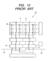
- FIG. 12 is a diagram illustrating the circuit configuration of a MOS type solid-state imaging apparatus 10 disclosed in Japanese Patent Application Laid-Open No. 2008-103992 .
- Japanese Patent Application Laid-Open No. 2008-103992 discloses a solid-state imaging apparatus including AD converters 16 and 17 for each of columns of pixels 30 in order to realize an increase in speed.
- the solid-state imaging apparatus disclosed in Japanese Patent Application Laid-Open No. 2008-103992 includes plural data buses 19 and 20 that transmit AD-converted digital signals for the pixels independently from each other and reads out the digital signals from the plural data buses 19 and 20 in parallel.
- Japanese Patent Application Laid-Open No. 2008-103992 also discloses a technique for dividing the pixels into two sections, a left section 11 and a right section 12, by a dividing line parallel to the columns and simultaneously reading out signals.
- pixels in which photoelectric conversion elements are shielded from light called OB (optical black) pixels are arranged in respective rows and outputs of the OB pixels are used for correction and the like in a direction parallel to the rows.
- OB pixels optical black pixels
- outputs of the OB pixels cannot be read out from an output terminal on the right side. Therefore, it is difficult to correct the outputs read out from the output terminal on the right side using the OB pixels.
- the document US 2007/0076109 A1 discloses a high-speed CMOS image sensor circuit with block memory readout.
- This image sensor circuit includes a pixel array, a plurality of column analog-to-digital conversion (ADC) circuits, and at least two memory blocks.
- Each column ADC circuit is connected to receive analog pixel signals provided from corresponding pixel circuits of the pixel array, and is configured to convert the received analog pixel signals into digital pixel signals.
- Each memory block is connected to receive digital pixel signals provided from corresponding column ADC circuits of the plurality of column ADC circuits.
- At least two of the at least two memory blocks are connected to receive digital pixel signals that are provided from corresponding column ADC circuits that are located to a same side of the pixel array.
- Each memory block of the at least two memory blocks includes a plurality of memory cells, one or more sense amplifiers connected to the memory cells by a readout bus, and a memory controller.
- a solid-state imaging apparatus as defined in the independent claim. Further developments and/or modifications of the solid-state imaging apparatus according to the present invention are defined in respective dependent claims. According to another aspect of the present invention, there is provided an imaging system including the solid-state imaging apparatus according to the present invention.
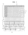
- FIG. 1 is a diagram of a basic circuit configuration example of a MOS type solid-state imaging apparatus according to a first embodiment of the present invention.
- Basic circuits of this configuration example are formed on the same substrate of silicon and configured as one solid-state imaging apparatus.
- a pixel region is a pixel region 101 with pixels arranged in 10 rows x 16 columns.
- One row at an upper end and two columns at a left end in this pixel region 101 are OB (optical black) pixels 101-1.
- Each of the OB pixels 101-1 has a photoelectric conversion element shielded from light.
- the other pixels in 9 rows x 14 columns are effective pixels 101-2.
- Reference numeral 102 denotes analog-to-digital converters (AD converters) provided to correspond to the columns of the pixel region 101.
- Reference numeral 103 denotes digital memories that temporarily store digital signals converted by the AD converters 102.
- Reference numeral 104 denotes block digital output lines.
- Reference numeral 108 denotes a common digital output line. Whereas only outputs from the digital memories 103 in the block are transmitted to the block digital output lines 104, digital outputs from the digital memories 103 in all the columns are transmitted to the common digital output line 108.
- Reference numeral 105 denotes buffer circuits that buffer signals read out from the digital memories 103 to the block digital output lines 104.
- Reference numeral 106 denotes block selecting units that control a readout connection relation among the blocks. Usually, the block selecting units 106 include changeover switches and buffer circuits.
- Reference numeral 107 denotes a horizontal scanning circuit that controls readout timing for the digital memories 103 in the respective columns.
- Reference numeral 109 denotes a vertical scanning circuit that controls readout timing for the pixels in the respective rows in the pixel region 101.
- As the circuit configuration of the horizontal scanning circuit 107 and the vertical scanning circuit 109 usually, a configuration of a shift register, a decoder or the like is used.
- Analog outputs from the pixels in the row in the pixel region 101 selected by the vertical scanning circuit 109 are analog-to-digital converted by the AD converters 102 corresponding to the respective columns.
- a result of the conversion is stored in the digital memories 103 corresponding to the respective columns as digital data.
- Readout order of the digital data stored in the digital memories 103 is selected by the horizontal scanning circuit 107.
- the digital data temporarily stored in the digital memory 103 is read out to the block digital output line 104.
- the data read out to the block digital output line 104 is read out to the common digital output line 108 via the buffer circuit 105 and the block selecting unit 106.
- the number of columns in the pixel region 101 is sixteen and the four block digital output lines 104 are provided. Therefore, four digital memories 103 are connected in parallel for each of the block digital output lines 104. On the other hand, if block division is not employed, sixteen digital memories 103 would be connected in parallel. Therefore, the number of digital memories 103 connected in parallel and the length of a digital output line would be quadrupled. In this embodiment, since the digital output line is divided, all of the wiring resistance and the wiring capacity of the block digital output lines 104 and the total capacity of the digital memories 103 connected together are quartered. It goes without saying that the capacity and the resistance of readout wires are substantial hindrances in performing high-speed readout. Therefore, it is extremely effective for an increase in speed to arrange the block digital output lines 104 and reducing the resistance and the capacity in the block digital output lines 104 as in this embodiment.
- FIGS. 2 to 4 are equivalent circuit diagrams illustrating examples of the buffer circuit 105 used in this embodiment. Since it is necessary to lay out the output circuits in the digital memory 103 at column pitches, it is usually difficult to increase a transistor size used in the output circuits. On the other hand, since the buffer circuits 105 only have to be laid out at pitches of the blocks, it is possible to relatively easily increase the transistor size.
- the digital output line is divided into the plural block digital output lines 104 to read out digital signals, load on the block digital output lines 104 driven by the output circuits of the digital memories 103 having small driving force can be reduced. It is possible to perform high-speed readout by driving the block digital output lines 104 to the common digital output line 108 with the buffer circuits 105 having large driving force.
- a circuit in FIG. 2 is an example of the buffer circuit 105 and is a CMOS inverter circuit.
- Reference numeral 201 denotes an input terminal of the buffer circuit 105
- 202 denotes an output terminal of the buffer circuit 105.
- FIG. 2 the circuit configuration of one stage of a CMOS inverter is illustrated as an example. However, a plurality of the CMOS inverters may be connected in series to increase driving force stepwise.
- a non-inverted buffer circuit can be configured by connecting CMOS inverters in even number stages in series.
- An inverted buffer circuit can be configured by connecting CMOS inverters in odd number stages in series. Any one of the configurations may be used.
- a circuit in FIG. 3 is a synchronizing delaying circuit (a flip-flop circuit) as another configuration examples of the buffer circuit 105. It is possible to regenerate a waveform by connecting the block digital output line 104 to an input terminal 301 and synchronizing the output of the block digital output line 104 with a clock input to a clock terminal 302. Even if a signal of the block digital output line 104 is delayed, since the waveform is regenerated in exchange for delaying data output by one clock, it is possible to read out the signal at high speed in terms of a readout frequency, although a clock delay occurs in the output.
- Reference numeral 303 denotes a reset input terminal and 304 denotes an output terminal.
- a circuit in FIG. 4 is a comparing circuit (a sense amplifier circuit) as another configuration examples of the buffer circuit 105.
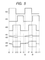
- FIG. 5 is a timing chart of driving timing for the comparing circuit.
- Reference numeral 400 denotes digital output line reset voltage.
- Reference numerals 401 and 402 denote buffer circuit differential input terminals.
- Reference numerals 406 and 407 denote buffer circuit differential output terminals.
- Reference numeral 403 denotes a latch pulse input terminal.
- Reference numeral 404 denotes a digital output line reset pulse input terminal.
- Reference numeral 405 denotes a latch pulse input terminal (inverting). An inverted signal of a pulse given to the latch pulse input terminal 403 is given to the latch pulse input terminal (inverting) 405.
- Reference numerals 408 to 411 and 415 to 417 denote PMOS transistors.
- Reference numerals 412 to 414 denote NMOS transistors.
- the two lines of the block digital output line 104 are connected to a non-inverted signal 401 and an inverted signal 402 in FIG. 4 .
- An input differential signal is input to the buffer circuit 105.
- reference numeral 403 denotes a latch signal and 404 denotes a reset signal. Since reference numeral 405 denotes an inverted signal of the latch signal 403, detailed description of timing of the signal 405 is omitted.
- Reference numerals 406 and 407 denote differential outputs of the sense amplifier.
- the output 406 is a non-inverted signal and the output 407 is an inverted signal.
- Reference numeral 500 in FIG. 5 denotes an enable pulse for enabling the outputs of the digital memories 103.
- An AND of the signal 500 and a column selected by the horizontal scanning circuit 107 is output timing of the digital memories 103.
- the enable pulse 500 changes to a high level and the outputs of the digital memories 103 are enabled.
- the nodes 401 and 402 change according to digital data temporarily stored in the digital memories 103.
- the digital data temporarily stored in the digital memory 103 is represented as 1 (high level)
- the non-inverted signal 401 transitions to the high level
- the inverted signal 402 transitions to a low level.
- the signals 401 and 402 are delayed and an amount of change per unit time decreases.
- the latch signal 403 is in a low level state until time t1.
- the PMOS transistors 408 and 409 are in an ON state and the NMOS transistor 414 and the PMOS transistor 415 are in an OFF state. Therefore, the nodes 406 and 407 are at the same level as the nodes 401 and 402 from time t0 to t1.
- the latch signal 403 changes to the high level and the NMOS transistor 414 and the PMOS transistor 415 change to the ON state.
- a latch circuit including the four MOS transistors 410, 411, 412, and 413 is enabled and a higher one of the nodes 406 and 407 changes to the high level and a lower one changes to the low level.
- a period of time t3 to t5 is a reset period. Readout from the digital memories 103 is not performed. In this period, the reset pulse 404 changes to the high level and initializes the nodes 401, 402, 406, and 407 to a reset level.
- Operation at time t6 and subsequent time is repetition of the operation at time t0 to t5.
- the digital memories 103 output data of 0 (the low level). Therefore, a relation of level between the nodes 401 and 402 is reversed and results of the nodes 406 and 407 as output results are also reversed.
- the data read out from the digital memories 103 and the block digital output line 104 by using the buffer circuit 105 in FIGS. 2 to 4 is output to the common digital output line 108 through the block selecting unit 106.
- the block selecting unit 106 is a circuit that switches a connection state among blocks when an output signal from the block digital output line 104 is output to the common digital output line 108.
- the circuit configuration of the block selecting unit 106 generally includes a switch for switching selection and a flip-flop circuit, for example, the flip-flop circuit illustrated in FIG. 3 .
- the block selecting unit 106 has a function of delaying a signal output by one clock and synchronizing a delay in a waveform besides the switching function.
- FIG. 6 is a timing chart illustrating a relation of readout between the block selecting unit 106 and the horizontal scanning circuit 107. Timing illustrated in FIG. 6 is described in detail below.
- a first bit of the horizontal scanning circuit 107 changes to the high level at time t0 to t1 and a second bit changes to the high level at time t1 to t2. Therefore, readouts from the digital memories 103 in corresponding columns are enabled. The same holds true at time t2 to t3 and subsequent time.
- a first block of the block selecting unit 106 is enabled at time t0 to t4 and a second block is enabled at time t4 to t7. In other words, at time t0 to t4, the block selecting unit 106 operates such that output from the first buffer circuit 105 from the left in FIG. 1 is output to the common digital output line 108.
- the block selecting unit 106 operates such that output from the second buffer circuit 105 from the left in FIG. 1 is output to the common digital output line 108. At time t7 and subsequent time, the block selecting unit 106 operates such that signals from adjacent blocks are sequentially output.
- a readout result of the digital memories 103 for the first bit enabled at time t0 to t1 is output through the block selecting unit 106. Consequently, the read out result is output to the common digital output line 108 with a delay of one clock with respect to a clock supplied from a clock generator 110 as a timing generating circuit. Similarly, readout results of the digital memories 103 of second to fourth bits are output to the common digital output line 108 with a delay of one clock.
- outputs of fifth to eighth bits are output to the common digital output line 108 through the switches of two block selecting units 106.
- output of a fifth bit selected at time t3 to t4 is output to the common digital output line 108 at time t5 to t6 with a delay of two clocks with respect to the clock supplied from the clock generator 110. Therefore, in this embodiment, a digital signal of a fourth bit and a digital signal of a fifth bit of the horizontal scanning circuit 107 are simultaneously changed to the high level with a difference in a delay in the respective blocks taken into account.
- periodicity of timing for enabling the bits of the horizontal scanning circuit 107 is changed at boundaries of the blocks.
- the timing for enabling the bits of the horizontal scanning circuit 107 is changed at the timing with a difference in the number of delays of clocks taken into account for each of the blocks. Therefore, it is possible to read out signals to the common digital output line 108 in order of the columns without a break.
- a result of the AD conversion is temporarily stored in the digital memories 103 and digital data of the result is read out.
- a format of analog output for not performing the AD conversion in an imaging apparatus when block output lines are provided as in this embodiment and buffer circuits are arranged in the respective block output lines, an image is deteriorated because of fluctuation among the blocks. This is because, in the respective blocks, very small changes in characteristics of the block output lines, the buffer circuits, and selecting circuits lead to a step (offset) among the blocks when output as an image. This problem is almost negligible in the readout format of this embodiment for handling digital data. Therefore, in this embodiment for reading out the digital data temporarily stored in the digital memories 103 after being AD-converted, it is possible to read out signals at high speed while suppressing deterioration in an image quality.
- the common digital output line 108 is arranged on the first bit side.
- an arrangement place of the common digital output line 108 is not limited to this. Although it is necessary to change timing of the block selecting circuit 106 and the horizontal scanning circuit 107, the same effects can be obtained irrespective of the arrangement place of the common digital output line 108 by adjusting the driving timing.
- a set of the AD converter 102 and the digital memory 103 is arranged for each of the pixel columns.
- the effects in this embodiment can be sufficiently obtained even if, for example, one AD converter is arranged for plural pixel columns or two or more AD converters are arranged for one pixel column as long as a relation between AD conversion speed and readout speed is satisfied.
- the digital memories 103 only have to have a function of temporarily storing AD-converted digital data.
- the clock generator 110 is provided in FIG. 1 .
- a counter circuit may be provided instead of the clock generator 110 and the digital memories 103 in the respective columns may latch (store) a counter output value of the counter circuit at timing of the digital memories 103.
- a clock generator that outputs a master clock may be provided instead of the clock generator 110 and the digital memories 103 may adopt a column counter format to store a count value for each of the columns.
- FIG. 7 is a block diagram illustrating a configuration example of a solid-state imaging apparatus according to a second embodiment of the present invention.
- FIG. 7 since circuit units same as those in FIG. 1 are denoted by the same reference numerals, explanation of the circuit units is omitted.
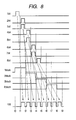
- FIG. 8 is a timing chart illustrating readout timing in the second embodiment.
- the horizontal scanning circuit 107 When the first bit is enabled, the horizontal scanning circuit 107 simultaneously performs read out from the digital memories 103 in the first column and the second column. In this embodiment, two channels of block digital output lines 104 and two channels of block selecting units 106 are also present. Parallel readout for two columns can be performed. Consequently, the horizontal scanning circuit 107 ends readout for sixteen columns in selecting operation for eight bits. This enables high-speed readout.
- a first bit of the horizontal scanning circuit 107 changes to a high level. According to this change, readout from the digital memories 103 in the first column and the second column are enabled. Similarly, when a second bit changes to the high level at time t1 to t2, readout from the digital memories 103 in the third column and the fourth column are enabled. The same holds true at time t2 to t3 and subsequent time.
- a first block of the block selecting unit 106 is enabled at time t0 to t2 and a second block is enabled at time t2 to t4.
- Readout results of the digital memories 103 in the first column and the second column enabled at time t0 to t1 are output through the block selecting unit 106. Consequently, the readout results are output to the common digital output lines 108 at time t1 to t2 with a delay of one clock with respect to a clock supplied from the clock generator 110.
- For the second bit in the same manner, readout results of the digital memories 103 in the third column and the fourth column are output to the common digital output lines 108 with a delay of one clock.
- Output denoted by reference numeral 108 in FIG. 8 indicates one of the two channels in FIG. 7 . Concerning the other channel, readout results are output at the same timing.
- Outputs for a third bit and a fourth bit are output to the common digital output lines 108 through switches of two block selecting circuits 106.
- outputs of the three bits selected at time t1 to t2 are output to the common digital output lines 108 at time t3 to t4 with a delay of two clocks with respect to the clock supplied from the clock generator 110.
- the second bit and the third bit are simultaneously enabled (changed to the high level) by the horizontal scanning circuit 107 at time t1 to t2, which is a boundary between the blocks, with a clock delay between the blocks taken into account.
- the same operation is repeated for a fifth bit and subsequent bits.
- the two channels of the common digital output lines 108 are provided.
- three or more channels of common digital output lines may be provided.
- all the readout circuits are arranged below the pixels to readout signals.
- the arrangement of the readout circuits is not limited to this.
- the AD converters 102 and the digital memories 103 may be arranged above and below the pixels in such a manner that those for the first bit are arranged above the pixel region and those for the second bit are arranged below the pixel region.
- two sets each of the block digital output lines 104, the buffer circuits 105, the block selecting units 106, the common digital output lines 108, and horizontal scanning circuits 107 may be arranged above and below the pixel region to perform readout in two channels.
- FIG. 9 is a block diagram illustrating a configuration example of a solid-state imaging apparatus according to a third embodiment of the present invention.
- circuit units same as those in FIG. 1 are denoted by the same reference numerals, explanation of the circuits is omitted.
- the block digital output lines 104 are connected to the buffer circuits 105 via the block selecting units 106.
- Concerning timing for readout in this embodiment signals can be read out at timing same as that in FIG. 6 described in the first embodiment. Therefore, detailed explanation of the timing is omitted.
- a differential format can be adopted for a format of a sense amplifier in the same manner as adopting the differential format for the output of the digital memory 103.
- the configuration including the sense amplifier since it is unnecessary to change the transmission of signals among the blocks to the full high level and to the full low level, it is possible to read out signals at high speed and low power consumption as described in the first embodiment.
- FIG. 10 is a block diagram illustrating a configuration example of a solid-state imaging apparatus according to a fourth embodiment of the present invention.
- FIG. 10 since circuit units same as those in FIG. 1 are denoted by the same reference numerals, explanation of the circuits is omitted.
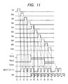
- FIG. 11 is a timing chart illustrating readout timing in the fourth embodiment.
- the horizontal scanning circuit 107 simultaneously changes the two bits to the high level. However, the horizontal scanning circuit 107 in this embodiment changes one bit to the high level at one timing.
- Reference numeral 111 denotes a selective delaying circuit, which is a logic circuit including a flip-flop circuit, a selecting circuit, and a multiplexer.
- a first bit of the horizontal scanning circuit 107 changes to the high level. According to the change, readout from the digital memory 103 in the first column is enabled. Similarly, a second bit changes to the high level at time t1 to t2, whereby readout from the digital memory 103 in the second column is enabled. The same holds true at time t2 to t3 and subsequent time.
- a first block of the block selecting unit 106 is enabled at time t0 to t4 and a second block is enabled at time t4 to t8.
- a readout result of the digital memory 103 in the first column enabled at time t0 to t1 is output through the buffer circuit 105. Consequently, a signal reaches an input terminal of the selective delaying circuit 111 at time t1 to t2 with a delay of one clock with respect to a clock supplied from the clock generator 110. Similarly, signals of second to fourth bits are input to the input terminal of the selective delaying circuit 111 with a delay of one clock with respect to the clock supplied from the clock generator 110.
- signals of fifth to eighth bits pass the buffer circuit 105 twice. Therefore, a delay of two clocks occurs until readout of the fifth to eighth bits reaches the input terminal of the selective delaying circuit 111. As a result, the signal of the fifth bit read out at time t4 to t5 reaches the input terminal of the selective delaying circuit 111 in a period of time t6 to t7.
- Signals of a ninth bit and subsequent bits are further delayed by one clock.
- Signals of a thirteenth bit and subsequent bit are further delayed by one clock than the signal of the ninth bit. Therefore, a gap of data occurs at the input terminal of the selective delaying circuit 111 at time such as a period of time t5 to t6 and a period of time t10 to t11.
- the selective delaying circuit 111 adjusts a delay based on a block switching signal of the horizontal scanning circuit 107. Specifically, the selective delaying circuit 111 delays signals of the first to fourth bits by three clocks and delays signals of the fifth to eighth bits by two clocks. By changing the delay for each of the blocks in this way, it is possible to output data without a break to the common output terminal 108 in order in which the pixels are arrayed.
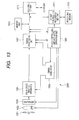
- FIG. 13 is a diagram illustrating a configuration example of an imaging system 1000 according to a fifth embodiment of the present invention using the solid-state imaging apparatus according to the embodiments.
- a solid-state imaging apparatus 1004 has a configuration including the solid-state imaging apparatus described in the embodiments and including other imaging signal processing circuits.
- the other imaging signal processing circuits are circuits for performing, for example, correction of offset, linearity, and fixed pattern noise, rearrangement for passing data to an output signal processing unit, and frequency conversion.
- a part or all of the imaging signal processing circuits may be formed on the outside of the solid-state imaging apparatus 1004.
- the solid-state imaging apparatus 1004 converts an optical image focused by a lens 1002 into image data.
- Reference numeral 1001 denotes a barrier functioning as both protection for the lens 1002 and a main switch.
- the lens 1002 is an optical system that focuses an optical image of a subject on the solid-state imaging apparatus 1004. An amount of light passing through the lens 1002 is changed by a diaphragm 1003.
- a signal processing unit 1007 applies various kinds of correction to the image data output from the solid-state imaging apparatus 1004 and compresses the data.
- a timing generator 1008 outputs various timing signals to the signal processing unit 1007.
- the circuits 1007 and 1008 may be formed on a chip on which the solid-state imaging apparatus 1004 is formed.
- the imaging system 1000 includes a whole controlling and arithmetic operation unit 1009 that controls various arithmetic operations and the entire imaging system 1000, a memory unit 1010 for temporarily storing image data, and a interface unit controlling recording medium 1011 for performing recording in and readout from a recording medium.
- the imaging system 1000 further includes a recording medium 1012 to which a semiconductor memory or the like for performing recording and readout of image data is detachably attachable and an external interface (I/F) unit 1013 for communicating with an external computer and the like.
- I/F external interface
- the operation of the imaging system 1000 illustrated in FIG. 13 is described below.
- a main power supply is turned on, a power supply for control systems such as the whole controlling and arithmetic operation unit 1009 is then turned on, and a power supply for imaging system circuits such as the solid-state imaging apparatus 1004 is further turned on.
- the imaging system 1000 performs operation for controlling an exposure amount.
- the whole controlling and arithmetic operation unit 1009 opens the diaphragm 1003.
- a signal output from the solid-state imaging apparatus 1004 at this point is input to the signal processing unit 1007.
- the signal processing unit 1007 causes the whole controlling and arithmetic operation unit 1009 to perform arithmetic operation for calculating exposure based on the signal.
- the signal processing unit 1007 determines the brightness of a subject according to a result of the arithmetic operation.
- the whole controlling and arithmetic operation unit 1009 controls the diaphragm 1003. This determination can be performed by, for example, comparing data stored in the whole controlling and arithmetic operation unit 1009 in advance.
- the whole controlling and arithmetic operation unit 1009 performs, based on the signal output from the solid-state imaging apparatus 1004, arithmetic operation for extracting a high-frequency component and calculating a distance to the subject. Thereafter, the whole controlling and arithmetic operation unit 1009 drives the lens 1002 and determines whether the lens 1002 is focused in the driven state. When it is determined that the lens 1002 is not focused, the whole controlling and arithmetic operation unit 1009 drives the lens 1002 again and performs ranging. This determination can be performed by, for example, comparing the data stored in the whole controlling and arithmetic operation unit 1009 in advance.
- Main exposure is started after it is determined that the lens 1002 is focused.
- an image signal output from the solid-state imaging apparatus 1004 is accumulated in the memory unit 1010 by the whole controlling and arithmetic operation unit 1009 after being processed by the signal processing unit 1007.
- data accumulated in the memory unit 1010 is recorded in the detachable recording medium 1012 such as a semiconductor memory via the recording medium control I/F unit 1011 according to the control by the whole controlling and arithmetic operation unit 1009.
- the data may be directly input to a computer or the like via the external I/F unit 1013.
- Each of the solid-state imaging apparatuses includes the pixel region 101 in which pixels that output analog signals are arranged in a matrix shape.
- the plural analog-to-digital converters 102 are provided to correspond to the columns of the pixel region 101 and convert analog signals obtained by photoelectric conversion of the plural pixels into digital signals.
- the plural digital memories 103 store the digital signals converted by the analog-to-digital converters 102. With the plural digital memories 103 set as blocks, the plural block digital output lines 104 are provided to correspond to the blocks and output the digital signals stored in the plural digital memories 103 included in the blocks.
- the common digital output line 108 outputs the digital signals from the plural block digital output lines 104.
- the buffer circuits 105 are provided between the block digital output lines 104 and the common digital output line 108 and buffer the digital signals output from the block digital output lines 104.
- the block selecting units 106 are provided between the block digital output lines 104 and the common digital output line 108 and can switch the block digital output lines 104 electrically connected to the common digital output line 108.
- the horizontal scanning circuit 107 controls readout order for the digital memories 103. In controlling the order, as illustrated in FIG. 11 , the horizontal scanning circuit 107 performs control such that the digital signals stored in the digital memories 103 are output to the common digital output line 108 in order in which the digital memories 103 are arrayed (the first bit to the tenth bit).
- the buffer circuit 105 illustrated in FIG. 2 includes the CMOS inverter.
- the buffer circuit 105 illustrated in FIG. 3 includes the synchronizing delaying circuit that synchronizes an input signal to a clock.
- the buffer circuit 105 illustrated in FIG. 4 includes the comparing circuit that compares input differential signals and decides logic.
- the selective delaying circuit 111 is provided between the common digital output line 108 and the block digital output line 104 and performs control of a delay for each of the blocks.
- the plural block digital output lines 104 are provided for each of the blocks.
- the digital signals stored in the plural digital memories 103 included in one block are output in parallel.
- the horizontal scanning circuit 107 performs control such that the digital signals stored in the adjacent digital memories 103 included in the adjacent blocks are output to the corresponding block digital output lines 104 at the same timing.
- the horizontal scanning circuit 107 controls readout timing for the digital memories 103 such that the output of the digital signals are not interrupted even in breaks of the blocks.
- the imaging system 1000 includes the solid-state imaging apparatus 1004 according to any one of the first to fourth embodiments, the optical system (lens) 1002 that forms an optical image in the pixel region 101, and the signal processing unit 1007 that processes a signal output from the solid-state imaging apparatus 1004.
- a solid-state imaging apparatus includes plural analog-to-digital converters (102) that convert analog signals obtained by photoelectric conversion into digital signals, plural digital memories (103) that store the digital signals converted by the analog-to-digital converters, plural block digital output lines (104) that are provided to correspond to blocks of the plural digital memories and to which the digital signals stored in the plural digital memories included in the blocks are output, a common digital output line (108) that outputs the digital signals output from the plural block digital output lines, buffer circuits (105) that buffer the digital signals output from the block digital output lines, and block selecting units (106) that can switch the block digital output lines electrically connected to the common digital output line.
Landscapes
- Engineering & Computer Science (AREA)
- Multimedia (AREA)
- Signal Processing (AREA)
- Transforming Light Signals Into Electric Signals (AREA)
- Solid State Image Pick-Up Elements (AREA)
- Facsimile Heads (AREA)
Claims (11)
- Dispositif d'acquisition d'image à semi-conducteurs comprenant :(a) une région (101) de pixels incluant une pluralité de pixels agencés en une matrice incluant une pluralité de colonnes de pixels, dans lequel chaque pixel effectue une conversion photoélectrique et sort un signal analogique ;(b) une pluralité de convertisseurs (102) d'analogique en numérique, dans lequel chaque convertisseur d'analogique en numérique convertit, en un signal numérique, le signal analogique sorti par l'un des pixels inclus dans l'une des colonnes de pixels, et dans lequel chaque convertisseur d'analogique en numérique est prévu en correspondance avec l'une, différente, des colonnes de pixels ;(c) une pluralité de mémoires numériques (103) agencées en une pluralité de blocs de deux ou plus mémoires numériques, dans lequel chaque mémoire numérique détient le signal numérique convertit par l'un, différent, des convertisseurs d'analogique en numérique, et dans lequel chacune des deux ou plus mémoires numériques est prévue en correspondance avec l'un, différent, des convertisseurs d'analogique en numérique ;(d) une pluralité de lignes (104) de sortie numérique de bloc, dans lequel chaque ligne de sortie numérique de bloc est raccordée à l'un, différent, des blocs de mémoires numériques, dans lequel le signal numérique détenu dans une mémoire numérique particulière est sorti par la ligne correspondante de sortie numérique de bloc ; et(e) une pluralité de circuits tampons (105), dans lequel chaque circuit tampon met en tampon un signal numérique issu de l'une, correspondante, des lignes de sortie numérique de bloc,
caractérisé en ce que :(f) le dispositif d'acquisition d'image à semi-conducteurs comprend en outre une pluralité d'unités (106) de sélection de bloc, dans lequel chaque unité de sélection de bloc est prévue en correspondance avec l'un, différent, des blocs de mémoires numériques, et dans lequel une première unité de sélection de bloc de la pluralité d'unités de sélection de bloc est constituée pour sortir sélectivement un signal numérique issu de l'une, correspondante, des lignes de sortie numérique de bloc, une deuxième unité de sélection de bloc de la pluralité d'unités de sélection de bloc est constituée pour sortir sélectivement le signal numérique sorti de la première unité de sélection de bloc et un signal numérique sorti de l'une, correspondante, des lignes de sortie numérique de bloc, et une troisième unité de sélection de bloc de la pluralité d'unités de sélection de bloc est constituée pour sortir sélectivement le signal numérique sorti de la deuxième unité de sélection de bloc et un signal numérique sorti de l'une, correspondante, des lignes de sortie numérique de bloc ; et(g) chacun des circuits tampons est connecté (1) entre l'une de la pluralité de lignes de sortie numérique de bloc et l'une de la pluralité d'unités de sélection de bloc, ou (2) à la sortie de l'une de la pluralité d'unités de sélection de bloc. - Dispositif d'acquisition d'image à semi-conducteurs selon la revendication 1, comprenant en outre un circuit de balayage horizontal qui commande la lecture des signaux numériques dans les mémoires numériques,
dans lequel le circuit de balayage horizontal opère de façon que les signaux numériques détenus dans les mémoires numériques soient lus, séquentiellement dans l'ordre d'agencement des mémoires numériques, à partir d'une ligne commune de sortie numérique. - Dispositif d'acquisition d'image à semi-conducteurs selon la revendication 1 ou 2, dans lequel chaque circuit tampon inclut un inverseur à CMOS.
- Dispositif d'acquisition d'image à semi-conducteurs selon la revendication 1 ou 2, dans lequel chaque circuit tampon inclut un circuit à retard de synchronisation qui synchronise, sur un signal d'horloge, le signal numérique sorti du circuit tampon.
- Dispositif d'acquisition d'image à semi-conducteurs selon la revendication 1 ou 2, dans lequel chaque circuit tampon inclut un circuit comparateur qui effectue une comparaison des sorties différentielles non inversée et inversée en tant que signaux numériques provenant de l'une des mémoires numériques, et détermine un résultat logique basé sur la comparaison.
- Dispositif d'acquisition d'image à semi-conducteurs selon l'une quelconque des revendications 1 à 5, dans lequel plus d'une des lignes de sortie numérique de bloc sont prévues pour chacun des blocs de mémoires numériques, de sorte que les signaux numériques détenus par les deux ou plus mémoires numériques incluses dans l'un des blocs sont sortis en parallèle.
- Dispositif d'acquisition d'image à semi-conducteurs selon la revendication 2, dans lequel le circuit de balayage horizontal commande la lecture des signaux numériques issus des mémoires numériques, de façon à lire, au même moment, vers des lignes correspondantes de sortie numérique de bloc, les signaux numériques détenus par des mémoires numériques adjacentes respectivement incluses dans des blocs adjacents.
- Dispositif d'acquisition d'image à semi-conducteurs selon l'une quelconque des revendications 1 à 6, comprenant en outre un circuit de retardement sélectif agencé entre chaque ligne de sortie numérique de bloc et une ligne commune de sortie numérique, qui commande un retard pour chacun des blocs.
- Dispositif d'acquisition d'image à semi-conducteurs selon la revendication 1, comprenant en outre une ligne commune de sortie numérique qui sort des signaux numériques issus de la pluralité de lignes de sortie numérique de bloc.
- Dispositif d'acquisition d'image à semi-conducteurs selon la revendication 1, dans lequel chacune des unités de sélection de bloc inclut un commutateur et un circuit tampon.
- Système de prise de vue dans lequel est incorporé le dispositif d'acquisition d'image à semi-conducteurs selon l'une quelconque des revendications 1 à 10, le système de prise de vue incluant :un système optique (1002) qui met au point une image optique sur la région de pixels du dispositif d'acquisition d'image à semi-conducteurs ; etune unité (1007) de traitement de signal qui traite un signal sorti du dispositif d'acquisition d'image à semi-conducteurs.
Applications Claiming Priority (1)
| Application Number | Priority Date | Filing Date | Title |
|---|---|---|---|
| JP2008321292A JP4891308B2 (ja) | 2008-12-17 | 2008-12-17 | 固体撮像装置及び固体撮像装置を用いた撮像システム |
Publications (3)
| Publication Number | Publication Date |
|---|---|
| EP2200270A2 EP2200270A2 (fr) | 2010-06-23 |
| EP2200270A3 EP2200270A3 (fr) | 2012-04-18 |
| EP2200270B1 true EP2200270B1 (fr) | 2015-09-09 |
Family
ID=42026305
Family Applications (1)
| Application Number | Title | Priority Date | Filing Date |
|---|---|---|---|
| EP09179285.3A Active EP2200270B1 (fr) | 2008-12-17 | 2009-12-15 | Appareil d'imagerie à l'état solide et système d'imagerie utilisant l'appareil d'imagerie à l'état solide |
Country Status (4)
| Country | Link |
|---|---|
| US (2) | US8325260B2 (fr) |
| EP (1) | EP2200270B1 (fr) |
| JP (1) | JP4891308B2 (fr) |
| CN (2) | CN102917186B (fr) |
Families Citing this family (56)
| Publication number | Priority date | Publication date | Assignee | Title |
|---|---|---|---|---|
| JP5094498B2 (ja) | 2008-03-27 | 2012-12-12 | キヤノン株式会社 | 固体撮像装置及び撮像システム |
| JP5511220B2 (ja) * | 2009-05-19 | 2014-06-04 | キヤノン株式会社 | 固体撮像装置 |
| JP5577887B2 (ja) | 2010-06-29 | 2014-08-27 | スズキ株式会社 | V型エンジンの燃料供給装置 |
| JP2012049911A (ja) * | 2010-08-27 | 2012-03-08 | Canon Inc | 光電変換装置および撮像システム |
| JP2012049912A (ja) * | 2010-08-27 | 2012-03-08 | Canon Inc | 光電変換装置および撮像システム |
| JP5671890B2 (ja) * | 2010-08-31 | 2015-02-18 | 株式会社ニコン | 撮像装置 |
| JP2012065032A (ja) * | 2010-09-14 | 2012-03-29 | Sony Corp | パワーゲート回路、固体撮像素子、およびカメラシステム |
| JP5856392B2 (ja) | 2011-06-06 | 2016-02-09 | キヤノン株式会社 | 固体撮像装置およびカメラ |
| JP5808162B2 (ja) * | 2011-06-23 | 2015-11-10 | キヤノン株式会社 | 撮像素子、撮像装置及び撮像素子の駆動方法 |
| JP5762199B2 (ja) | 2011-07-28 | 2015-08-12 | キヤノン株式会社 | 固体撮像装置 |
| JP5901186B2 (ja) | 2011-09-05 | 2016-04-06 | キヤノン株式会社 | 固体撮像装置及びその駆動方法 |
| JP5858695B2 (ja) | 2011-09-08 | 2016-02-10 | キヤノン株式会社 | 固体撮像装置及び固体撮像装置の駆動方法 |
| JP5806566B2 (ja) | 2011-09-15 | 2015-11-10 | キヤノン株式会社 | A/d変換器および固体撮像装置 |
| JP5801665B2 (ja) | 2011-09-15 | 2015-10-28 | キヤノン株式会社 | 固体撮像装置、a/d変換器およびその制御方法 |
| JP5484422B2 (ja) | 2011-10-07 | 2014-05-07 | キヤノン株式会社 | 固体撮像装置 |
| JP5901212B2 (ja) | 2011-10-07 | 2016-04-06 | キヤノン株式会社 | 光電変換システム |
| JP5930651B2 (ja) | 2011-10-07 | 2016-06-08 | キヤノン株式会社 | 固体撮像装置 |
| JP5967955B2 (ja) | 2012-01-31 | 2016-08-10 | キヤノン株式会社 | 光電変換装置および撮像システム |
| JP5979896B2 (ja) | 2012-02-09 | 2016-08-31 | キヤノン株式会社 | 固体撮像装置 |
| JP6023437B2 (ja) | 2012-02-29 | 2016-11-09 | キヤノン株式会社 | 固体撮像装置及びカメラ |
| JP6025348B2 (ja) * | 2012-03-07 | 2016-11-16 | キヤノン株式会社 | 信号伝送装置、光電変換装置および撮像システム |
| JP6004685B2 (ja) | 2012-03-19 | 2016-10-12 | キヤノン株式会社 | 固体撮像装置及びその駆動方法 |
| JP6099893B2 (ja) | 2012-07-10 | 2017-03-22 | キヤノン株式会社 | 画像形成装置 |
| JP6049332B2 (ja) | 2012-07-11 | 2016-12-21 | キヤノン株式会社 | 光電変換装置および撮像システム |
| JP5980080B2 (ja) * | 2012-10-02 | 2016-08-31 | キヤノン株式会社 | 光電変換装置、撮像システム、光電変換装置の検査方法および撮像システムの製造方法 |
| JP6319946B2 (ja) | 2013-04-18 | 2018-05-09 | キヤノン株式会社 | 固体撮像装置及び撮像システム |
| JP6100074B2 (ja) | 2013-04-25 | 2017-03-22 | キヤノン株式会社 | 光電変換装置及び撮像システム |
| JP6174901B2 (ja) | 2013-05-10 | 2017-08-02 | キヤノン株式会社 | 固体撮像装置及びカメラ |
| JP6274788B2 (ja) | 2013-08-28 | 2018-02-07 | キヤノン株式会社 | 撮像装置、撮像システム及び撮像装置の駆動方法 |
| JP5886806B2 (ja) | 2013-09-17 | 2016-03-16 | キヤノン株式会社 | 固体撮像装置 |
| KR102105409B1 (ko) | 2013-12-09 | 2020-05-29 | 삼성전자주식회사 | 이종의 아날로그-디지털 컨버터를 포함하는 이미지 센서 |
| JP6239975B2 (ja) | 2013-12-27 | 2017-11-29 | キヤノン株式会社 | 固体撮像装置及びそれを用いた撮像システム |
| JP6246004B2 (ja) | 2014-01-30 | 2017-12-13 | キヤノン株式会社 | 固体撮像装置 |
| JP6412328B2 (ja) | 2014-04-01 | 2018-10-24 | キヤノン株式会社 | 固体撮像装置およびカメラ |
| JP6482186B2 (ja) | 2014-05-23 | 2019-03-13 | キヤノン株式会社 | 撮像装置及びその駆動方法 |
| JP6109125B2 (ja) | 2014-08-20 | 2017-04-05 | キヤノン株式会社 | 半導体装置、固体撮像装置、および撮像システム |
| JP6415187B2 (ja) | 2014-08-29 | 2018-10-31 | キヤノン株式会社 | 固体撮像装置および撮像システム |
| US9979916B2 (en) | 2014-11-21 | 2018-05-22 | Canon Kabushiki Kaisha | Imaging apparatus and imaging system |
| JP6480768B2 (ja) | 2015-03-17 | 2019-03-13 | キヤノン株式会社 | 固体撮像装置及びその駆動方法 |
| JP6499006B2 (ja) * | 2015-05-07 | 2019-04-10 | 株式会社半導体エネルギー研究所 | 撮像装置 |
| US9843756B2 (en) | 2015-05-27 | 2017-12-12 | Samsung Electronics Co., Ltd. | Imaging devices, arrays of pixels receiving photocharges in bulk of select transistor, and methods |
| JP6727771B2 (ja) | 2015-08-13 | 2020-07-22 | キヤノン株式会社 | 撮像装置 |
| JP6650779B2 (ja) * | 2016-02-19 | 2020-02-19 | キヤノン株式会社 | 撮像装置、撮像システム、撮像装置の駆動方法 |
| JP7005125B2 (ja) | 2016-04-22 | 2022-01-21 | キヤノン株式会社 | 撮像素子、撮像システム、および撮像素子の製造方法 |
| CN109076178B (zh) * | 2016-05-11 | 2021-07-13 | 索尼公司 | 固态图像拾取元件和电子设备 |
| CN106375688B (zh) * | 2016-09-06 | 2019-11-22 | 上海集成电路研发中心有限公司 | 一种cmos图像传感器及其信号传输方法 |
| JP6351691B2 (ja) * | 2016-11-17 | 2018-07-04 | キヤノン株式会社 | 光電変換装置および撮像システム |
| JP6877203B2 (ja) | 2017-03-24 | 2021-05-26 | キヤノン株式会社 | 撮像装置および移動体 |
| US10834354B2 (en) | 2018-06-25 | 2020-11-10 | Canon Kabushiki Kaisha | Imaging device, imaging system, movable object, and signal processing device |
| JP7245014B2 (ja) | 2018-09-10 | 2023-03-23 | キヤノン株式会社 | 固体撮像装置、撮像システム、および固体撮像装置の駆動方法 |
| JP6749728B2 (ja) * | 2018-09-25 | 2020-09-02 | キヤノン株式会社 | 固体撮像装置、その駆動方法およびカメラ |
| JP7353752B2 (ja) | 2018-12-06 | 2023-10-02 | キヤノン株式会社 | 光電変換装置及び撮像システム |
| JP7303682B2 (ja) | 2019-07-19 | 2023-07-05 | キヤノン株式会社 | 光電変換装置及び撮像システム |
| JP7374639B2 (ja) | 2019-07-19 | 2023-11-07 | キヤノン株式会社 | 光電変換装置及び撮像システム |
| JP7483454B2 (ja) | 2020-03-26 | 2024-05-15 | キヤノン株式会社 | 光電変換装置、撮像システム、移動体 |
| CN113497905B (zh) | 2020-04-01 | 2024-03-12 | 佳能株式会社 | 光电转换设备、成像系统和移动物体 |
Citations (2)
| Publication number | Priority date | Publication date | Assignee | Title |
|---|---|---|---|---|
| US6020760A (en) * | 1997-07-16 | 2000-02-01 | Altera Corporation | I/O buffer circuit with pin multiplexing |
| US20070076109A1 (en) * | 2005-10-04 | 2007-04-05 | Alexander Krymski | High speed CMOS image sensor circuits with block memory readout |
Family Cites Families (39)
| Publication number | Priority date | Publication date | Assignee | Title |
|---|---|---|---|---|
| US5043821A (en) * | 1988-08-31 | 1991-08-27 | Canon Kabushiki Kaisha | Image pickup device having a frame-size memory |
| JP2988095B2 (ja) | 1991-12-18 | 1999-12-06 | ソニー株式会社 | 固体撮像装置 |
| JPH05328039A (ja) | 1992-05-25 | 1993-12-10 | Ricoh Co Ltd | 画像読取装置 |
| JPH10206553A (ja) * | 1997-01-17 | 1998-08-07 | Canon Inc | 固体撮像装置及びx線固体撮像装置 |
| US6115066A (en) * | 1997-06-12 | 2000-09-05 | International Business Machines Corporation | Image sensor with direct digital correlated sampling |
| TW421962B (en) * | 1997-09-29 | 2001-02-11 | Canon Kk | Image sensing device using mos type image sensing elements |
| JPH11261046A (ja) * | 1998-03-12 | 1999-09-24 | Canon Inc | 固体撮像装置 |
| US6433822B1 (en) * | 1998-03-31 | 2002-08-13 | Intel Corporation | Method and apparatus for self-calibration and fixed-pattern noise removal in imager integrated circuits |
| KR100314801B1 (ko) * | 1998-12-22 | 2002-01-15 | 박종섭 | 이미지센서에서화면을패닝및스켈링하기위한장치 |
| US7009163B2 (en) * | 2001-06-22 | 2006-03-07 | Orbotech Ltd. | High-sensitivity optical scanning using memory integration |
| US7429764B2 (en) * | 2002-02-27 | 2008-09-30 | Canon Kabushiki Kaisha | Signal processing device and image pickup apparatus using the same |
| JP3728260B2 (ja) * | 2002-02-27 | 2005-12-21 | キヤノン株式会社 | 光電変換装置及び撮像装置 |
| JP4601897B2 (ja) * | 2002-11-13 | 2010-12-22 | ソニー株式会社 | 固体撮像装置及びその駆動方法 |
| JP4514188B2 (ja) * | 2003-11-10 | 2010-07-28 | キヤノン株式会社 | 光電変換装置及び撮像装置 |
| JP3793202B2 (ja) * | 2004-02-02 | 2006-07-05 | キヤノン株式会社 | 固体撮像装置 |
| JP4067054B2 (ja) * | 2004-02-13 | 2008-03-26 | キヤノン株式会社 | 固体撮像装置および撮像システム |
| US7423790B2 (en) * | 2004-03-18 | 2008-09-09 | Canon Kabushiki Kaisha | Photoelectric conversion apparatus and contact-type image sensor |
| JP4419681B2 (ja) | 2004-05-19 | 2010-02-24 | ソニー株式会社 | 固体撮像装置 |
| JP4971586B2 (ja) * | 2004-09-01 | 2012-07-11 | キヤノン株式会社 | 固体撮像装置 |
| JP5089017B2 (ja) * | 2004-09-01 | 2012-12-05 | キヤノン株式会社 | 固体撮像装置及び固体撮像システム |
| JP2006238444A (ja) * | 2005-02-22 | 2006-09-07 | Samsung Electronics Co Ltd | アクティブピクセルイメージセンサ |
| US20060186315A1 (en) | 2005-02-22 | 2006-08-24 | Kany-Bok Lee | Active pixel image sensors |
| GB2438693B (en) * | 2005-03-30 | 2009-07-08 | Micron Technology Inc | High density row ram for column parallel CMOS image sensors |
| JP4524652B2 (ja) | 2005-07-06 | 2010-08-18 | ソニー株式会社 | Ad変換装置並びに半導体装置 |
| JP4469806B2 (ja) * | 2006-03-06 | 2010-06-02 | キヤノン株式会社 | 撮像装置 |
| JP4804254B2 (ja) * | 2006-07-26 | 2011-11-02 | キヤノン株式会社 | 光電変換装置及び撮像装置 |
| JP5132102B2 (ja) * | 2006-08-01 | 2013-01-30 | キヤノン株式会社 | 光電変換装置および光電変換装置を用いた撮像システム |
| JP5123601B2 (ja) * | 2006-08-31 | 2013-01-23 | キヤノン株式会社 | 光電変換装置 |
| JP2008103992A (ja) | 2006-10-19 | 2008-05-01 | Matsushita Electric Ind Co Ltd | 固体撮像装置 |
| JP4893320B2 (ja) | 2007-01-12 | 2012-03-07 | ソニー株式会社 | 固体撮像装置、撮像装置 |
| JP4110193B1 (ja) * | 2007-05-02 | 2008-07-02 | キヤノン株式会社 | 固体撮像装置および撮像システム |
| JP4458113B2 (ja) * | 2007-05-02 | 2010-04-28 | ソニー株式会社 | データ転送回路、固体撮像素子、およびカメラシステム |
| JP2008294913A (ja) | 2007-05-28 | 2008-12-04 | Panasonic Corp | 固体撮像装置およびその駆動方法 |
| JP5040449B2 (ja) * | 2007-05-31 | 2012-10-03 | 富士通セミコンダクター株式会社 | 固体撮像素子および固体撮像素子を用いた信号処理方法 |
| JP5180537B2 (ja) * | 2007-08-24 | 2013-04-10 | キヤノン株式会社 | 光電変換装置及びマルチチップイメージセンサ |
| JP5268389B2 (ja) * | 2008-02-28 | 2013-08-21 | キヤノン株式会社 | 固体撮像装置、その駆動方法及び撮像システム |
| JP4500862B2 (ja) * | 2008-04-11 | 2010-07-14 | キヤノン株式会社 | 固体撮像装置の駆動方法 |
| JP5279352B2 (ja) * | 2008-06-06 | 2013-09-04 | キヤノン株式会社 | 固体撮像装置 |
| JP2010016056A (ja) * | 2008-07-01 | 2010-01-21 | Canon Inc | 光電変換装置 |
-
2008
- 2008-12-17 JP JP2008321292A patent/JP4891308B2/ja not_active Expired - Fee Related
-
2009
- 2009-12-01 US US12/628,271 patent/US8325260B2/en active Active
- 2009-12-14 CN CN201210334359.3A patent/CN102917186B/zh active Active
- 2009-12-14 CN CN2009102583511A patent/CN101753864B/zh active Active
- 2009-12-15 EP EP09179285.3A patent/EP2200270B1/fr active Active
-
2012
- 2012-11-06 US US13/670,175 patent/US8810706B2/en active Active
Patent Citations (2)
| Publication number | Priority date | Publication date | Assignee | Title |
|---|---|---|---|---|
| US6020760A (en) * | 1997-07-16 | 2000-02-01 | Altera Corporation | I/O buffer circuit with pin multiplexing |
| US20070076109A1 (en) * | 2005-10-04 | 2007-04-05 | Alexander Krymski | High speed CMOS image sensor circuits with block memory readout |
Also Published As
| Publication number | Publication date |
|---|---|
| US20100149394A1 (en) | 2010-06-17 |
| EP2200270A2 (fr) | 2010-06-23 |
| JP2010147684A (ja) | 2010-07-01 |
| US8810706B2 (en) | 2014-08-19 |
| US8325260B2 (en) | 2012-12-04 |
| CN102917186B (zh) | 2015-12-02 |
| JP4891308B2 (ja) | 2012-03-07 |
| CN101753864B (zh) | 2012-10-10 |
| EP2200270A3 (fr) | 2012-04-18 |
| CN101753864A (zh) | 2010-06-23 |
| US20130063639A1 (en) | 2013-03-14 |
| CN102917186A (zh) | 2013-02-06 |
Similar Documents
| Publication | Publication Date | Title |
|---|---|---|
| EP2200270B1 (fr) | Appareil d'imagerie à l'état solide et système d'imagerie utilisant l'appareil d'imagerie à l'état solide | |
| US8890990B2 (en) | Solid-state image pickup device and camera system | |
| US8735796B2 (en) | Solid-state imaging device comprising an analog to digital converter with column comparison circuits, column counter circuits, first and second inverters, and buffers | |
| US11595606B2 (en) | Photoelectric conversion apparatus and image capturing apparatus with A/D conversion and data transmission | |
| US8922692B2 (en) | Photoelectric conversion apparatus and image pickup system | |
| US8618461B2 (en) | Solid-state imaging device and imaging device | |
| KR20070091553A (ko) | 고체 촬상 장치, 고체 촬상 장치 구동 방법, 및 카메라 | |
| US20120104233A1 (en) | Solid-state imaging device and method of driving the same | |
| US8804020B2 (en) | Photoelectric conversion apparatus and image pickup system | |
| JP6025348B2 (ja) | 信号伝送装置、光電変換装置および撮像システム | |
| US20140192242A1 (en) | Image pickup apparatus, image pickup system and driving method of image pickup apparatus | |
| KR20080097944A (ko) | 데이터 전송 회로, 고체 촬상 소자, 및 카메라 시스템 | |
| KR101267666B1 (ko) | 고체 촬상 장치, 고체 촬상 장치의 구동 방법 및 촬상 장치 | |
| US9313426B2 (en) | Photoelectric conversion device and imaging system | |
| JP2007150448A (ja) | 固体撮像素子とその駆動方法、及びカメラモジュール | |
| JP5340373B2 (ja) | 固体撮像装置及び固体撮像装置を用いた撮像システム |
Legal Events
| Date | Code | Title | Description |
|---|---|---|---|
| PUAI | Public reference made under article 153(3) epc to a published international application that has entered the european phase |
Free format text: ORIGINAL CODE: 0009012 |
|
| AK | Designated contracting states |
Kind code of ref document: A2 Designated state(s): AT BE BG CH CY CZ DE DK EE ES FI FR GB GR HR HU IE IS IT LI LT LU LV MC MK MT NL NO PL PT RO SE SI SK SM TR |
|
| AX | Request for extension of the european patent |
Extension state: AL BA RS |
|
| PUAL | Search report despatched |
Free format text: ORIGINAL CODE: 0009013 |
|
| RIC1 | Information provided on ipc code assigned before grant |
Ipc: H04N 5/335 20110101AFI20120308BHEP |
|
| AK | Designated contracting states |
Kind code of ref document: A3 Designated state(s): AT BE BG CH CY CZ DE DK EE ES FI FR GB GR HR HU IE IS IT LI LT LU LV MC MK MT NL NO PL PT RO SE SI SK SM TR |
|
| AX | Request for extension of the european patent |
Extension state: AL BA RS |
|
| 17P | Request for examination filed |
Effective date: 20121018 |
|
| 17Q | First examination report despatched |
Effective date: 20140422 |
|
| REG | Reference to a national code |
Ref country code: DE Ref legal event code: R079 Ref document number: 602009033491 Country of ref document: DE Free format text: PREVIOUS MAIN CLASS: H04N0005217000 Ipc: H04N0005374000 |
|
| RIC1 | Information provided on ipc code assigned before grant |
Ipc: H04N 5/374 20110101AFI20140901BHEP |
|
| GRAP | Despatch of communication of intention to grant a patent |
Free format text: ORIGINAL CODE: EPIDOSNIGR1 |
|
| INTG | Intention to grant announced |
Effective date: 20150331 |
|
| GRAS | Grant fee paid |
Free format text: ORIGINAL CODE: EPIDOSNIGR3 |
|
| GRAA | (expected) grant |
Free format text: ORIGINAL CODE: 0009210 |
|
| AK | Designated contracting states |
Kind code of ref document: B1 Designated state(s): AT BE BG CH CY CZ DE DK EE ES FI FR GB GR HR HU IE IS IT LI LT LU LV MC MK MT NL NO PL PT RO SE SI SK SM TR |
|
| REG | Reference to a national code |
Ref country code: GB Ref legal event code: FG4D |
|
| REG | Reference to a national code |
Ref country code: AT Ref legal event code: REF Ref document number: 748940 Country of ref document: AT Kind code of ref document: T Effective date: 20150915 Ref country code: CH Ref legal event code: EP |
|
| REG | Reference to a national code |
Ref country code: IE Ref legal event code: FG4D |
|
| REG | Reference to a national code |
Ref country code: DE Ref legal event code: R096 Ref document number: 602009033491 Country of ref document: DE |
|
| REG | Reference to a national code |
Ref country code: NL Ref legal event code: MP Effective date: 20150909 |
|
| PG25 | Lapsed in a contracting state [announced via postgrant information from national office to epo] |
Ref country code: NO Free format text: LAPSE BECAUSE OF FAILURE TO SUBMIT A TRANSLATION OF THE DESCRIPTION OR TO PAY THE FEE WITHIN THE PRESCRIBED TIME-LIMIT Effective date: 20151209 Ref country code: LV Free format text: LAPSE BECAUSE OF FAILURE TO SUBMIT A TRANSLATION OF THE DESCRIPTION OR TO PAY THE FEE WITHIN THE PRESCRIBED TIME-LIMIT Effective date: 20150909 Ref country code: FI Free format text: LAPSE BECAUSE OF FAILURE TO SUBMIT A TRANSLATION OF THE DESCRIPTION OR TO PAY THE FEE WITHIN THE PRESCRIBED TIME-LIMIT Effective date: 20150909 Ref country code: GR Free format text: LAPSE BECAUSE OF FAILURE TO SUBMIT A TRANSLATION OF THE DESCRIPTION OR TO PAY THE FEE WITHIN THE PRESCRIBED TIME-LIMIT Effective date: 20151210 Ref country code: LT Free format text: LAPSE BECAUSE OF FAILURE TO SUBMIT A TRANSLATION OF THE DESCRIPTION OR TO PAY THE FEE WITHIN THE PRESCRIBED TIME-LIMIT Effective date: 20150909 |
|
| REG | Reference to a national code |
Ref country code: LT Ref legal event code: MG4D |
|
| REG | Reference to a national code |
Ref country code: AT Ref legal event code: MK05 Ref document number: 748940 Country of ref document: AT Kind code of ref document: T Effective date: 20150909 |
|
| PG25 | Lapsed in a contracting state [announced via postgrant information from national office to epo] |
Ref country code: HR Free format text: LAPSE BECAUSE OF FAILURE TO SUBMIT A TRANSLATION OF THE DESCRIPTION OR TO PAY THE FEE WITHIN THE PRESCRIBED TIME-LIMIT Effective date: 20150909 Ref country code: SE Free format text: LAPSE BECAUSE OF FAILURE TO SUBMIT A TRANSLATION OF THE DESCRIPTION OR TO PAY THE FEE WITHIN THE PRESCRIBED TIME-LIMIT Effective date: 20150909 Ref country code: ES Free format text: LAPSE BECAUSE OF FAILURE TO SUBMIT A TRANSLATION OF THE DESCRIPTION OR TO PAY THE FEE WITHIN THE PRESCRIBED TIME-LIMIT Effective date: 20150909 |
|
| PG25 | Lapsed in a contracting state [announced via postgrant information from national office to epo] |
Ref country code: NL Free format text: LAPSE BECAUSE OF FAILURE TO SUBMIT A TRANSLATION OF THE DESCRIPTION OR TO PAY THE FEE WITHIN THE PRESCRIBED TIME-LIMIT Effective date: 20150909 |
|
| PG25 | Lapsed in a contracting state [announced via postgrant information from national office to epo] |
Ref country code: CZ Free format text: LAPSE BECAUSE OF FAILURE TO SUBMIT A TRANSLATION OF THE DESCRIPTION OR TO PAY THE FEE WITHIN THE PRESCRIBED TIME-LIMIT Effective date: 20150909 Ref country code: EE Free format text: LAPSE BECAUSE OF FAILURE TO SUBMIT A TRANSLATION OF THE DESCRIPTION OR TO PAY THE FEE WITHIN THE PRESCRIBED TIME-LIMIT Effective date: 20150909 Ref country code: IT Free format text: LAPSE BECAUSE OF FAILURE TO SUBMIT A TRANSLATION OF THE DESCRIPTION OR TO PAY THE FEE WITHIN THE PRESCRIBED TIME-LIMIT Effective date: 20150909 Ref country code: IS Free format text: LAPSE BECAUSE OF FAILURE TO SUBMIT A TRANSLATION OF THE DESCRIPTION OR TO PAY THE FEE WITHIN THE PRESCRIBED TIME-LIMIT Effective date: 20160109 Ref country code: SK Free format text: LAPSE BECAUSE OF FAILURE TO SUBMIT A TRANSLATION OF THE DESCRIPTION OR TO PAY THE FEE WITHIN THE PRESCRIBED TIME-LIMIT Effective date: 20150909 |
|
| PG25 | Lapsed in a contracting state [announced via postgrant information from national office to epo] |
Ref country code: PT Free format text: LAPSE BECAUSE OF FAILURE TO SUBMIT A TRANSLATION OF THE DESCRIPTION OR TO PAY THE FEE WITHIN THE PRESCRIBED TIME-LIMIT Effective date: 20160111 Ref country code: PL Free format text: LAPSE BECAUSE OF FAILURE TO SUBMIT A TRANSLATION OF THE DESCRIPTION OR TO PAY THE FEE WITHIN THE PRESCRIBED TIME-LIMIT Effective date: 20150909 Ref country code: BE Free format text: LAPSE BECAUSE OF NON-PAYMENT OF DUE FEES Effective date: 20151231 Ref country code: RO Free format text: LAPSE BECAUSE OF FAILURE TO SUBMIT A TRANSLATION OF THE DESCRIPTION OR TO PAY THE FEE WITHIN THE PRESCRIBED TIME-LIMIT Effective date: 20150909 Ref country code: AT Free format text: LAPSE BECAUSE OF FAILURE TO SUBMIT A TRANSLATION OF THE DESCRIPTION OR TO PAY THE FEE WITHIN THE PRESCRIBED TIME-LIMIT Effective date: 20150909 |
|
| REG | Reference to a national code |
Ref country code: DE Ref legal event code: R097 Ref document number: 602009033491 Country of ref document: DE |
|
| PLBE | No opposition filed within time limit |
Free format text: ORIGINAL CODE: 0009261 |
|
| STAA | Information on the status of an ep patent application or granted ep patent |
Free format text: STATUS: NO OPPOSITION FILED WITHIN TIME LIMIT |
|
| PG25 | Lapsed in a contracting state [announced via postgrant information from national office to epo] |
Ref country code: MC Free format text: LAPSE BECAUSE OF FAILURE TO SUBMIT A TRANSLATION OF THE DESCRIPTION OR TO PAY THE FEE WITHIN THE PRESCRIBED TIME-LIMIT Effective date: 20150909 Ref country code: LU Free format text: LAPSE BECAUSE OF FAILURE TO SUBMIT A TRANSLATION OF THE DESCRIPTION OR TO PAY THE FEE WITHIN THE PRESCRIBED TIME-LIMIT Effective date: 20151215 |
|
| REG | Reference to a national code |
Ref country code: CH Ref legal event code: PL |
|
| 26N | No opposition filed |
Effective date: 20160610 |
|
| PG25 | Lapsed in a contracting state [announced via postgrant information from national office to epo] |
Ref country code: SI Free format text: LAPSE BECAUSE OF FAILURE TO SUBMIT A TRANSLATION OF THE DESCRIPTION OR TO PAY THE FEE WITHIN THE PRESCRIBED TIME-LIMIT Effective date: 20150909 Ref country code: DK Free format text: LAPSE BECAUSE OF FAILURE TO SUBMIT A TRANSLATION OF THE DESCRIPTION OR TO PAY THE FEE WITHIN THE PRESCRIBED TIME-LIMIT Effective date: 20150909 |
|
| REG | Reference to a national code |
Ref country code: IE Ref legal event code: MM4A |
|
| PG25 | Lapsed in a contracting state [announced via postgrant information from national office to epo] |
Ref country code: CH Free format text: LAPSE BECAUSE OF NON-PAYMENT OF DUE FEES Effective date: 20151231 Ref country code: LI Free format text: LAPSE BECAUSE OF NON-PAYMENT OF DUE FEES Effective date: 20151231 Ref country code: IE Free format text: LAPSE BECAUSE OF NON-PAYMENT OF DUE FEES Effective date: 20151215 |
|
| REG | Reference to a national code |
Ref country code: FR Ref legal event code: PLFP Year of fee payment: 8 |
|
| PG25 | Lapsed in a contracting state [announced via postgrant information from national office to epo] |
Ref country code: BE Free format text: LAPSE BECAUSE OF FAILURE TO SUBMIT A TRANSLATION OF THE DESCRIPTION OR TO PAY THE FEE WITHIN THE PRESCRIBED TIME-LIMIT Effective date: 20150909 |
|
| PG25 | Lapsed in a contracting state [announced via postgrant information from national office to epo] |
Ref country code: HU Free format text: LAPSE BECAUSE OF FAILURE TO SUBMIT A TRANSLATION OF THE DESCRIPTION OR TO PAY THE FEE WITHIN THE PRESCRIBED TIME-LIMIT; INVALID AB INITIO Effective date: 20091215 Ref country code: SM Free format text: LAPSE BECAUSE OF FAILURE TO SUBMIT A TRANSLATION OF THE DESCRIPTION OR TO PAY THE FEE WITHIN THE PRESCRIBED TIME-LIMIT Effective date: 20150909 Ref country code: BG Free format text: LAPSE BECAUSE OF FAILURE TO SUBMIT A TRANSLATION OF THE DESCRIPTION OR TO PAY THE FEE WITHIN THE PRESCRIBED TIME-LIMIT Effective date: 20150909 |
|
| PG25 | Lapsed in a contracting state [announced via postgrant information from national office to epo] |
Ref country code: CY Free format text: LAPSE BECAUSE OF FAILURE TO SUBMIT A TRANSLATION OF THE DESCRIPTION OR TO PAY THE FEE WITHIN THE PRESCRIBED TIME-LIMIT Effective date: 20150909 |
|
| PG25 | Lapsed in a contracting state [announced via postgrant information from national office to epo] |
Ref country code: MT Free format text: LAPSE BECAUSE OF FAILURE TO SUBMIT A TRANSLATION OF THE DESCRIPTION OR TO PAY THE FEE WITHIN THE PRESCRIBED TIME-LIMIT Effective date: 20150909 Ref country code: TR Free format text: LAPSE BECAUSE OF FAILURE TO SUBMIT A TRANSLATION OF THE DESCRIPTION OR TO PAY THE FEE WITHIN THE PRESCRIBED TIME-LIMIT Effective date: 20150909 |
|
| REG | Reference to a national code |
Ref country code: FR Ref legal event code: PLFP Year of fee payment: 9 |
|
| PGFP | Annual fee paid to national office [announced via postgrant information from national office to epo] |
Ref country code: FR Payment date: 20171229 Year of fee payment: 9 |
|
| PG25 | Lapsed in a contracting state [announced via postgrant information from national office to epo] |
Ref country code: MK Free format text: LAPSE BECAUSE OF FAILURE TO SUBMIT A TRANSLATION OF THE DESCRIPTION OR TO PAY THE FEE WITHIN THE PRESCRIBED TIME-LIMIT Effective date: 20150909 |
|
| PG25 | Lapsed in a contracting state [announced via postgrant information from national office to epo] |
Ref country code: FR Free format text: LAPSE BECAUSE OF NON-PAYMENT OF DUE FEES Effective date: 20181231 |
|
| REG | Reference to a national code |
Ref country code: DE Ref legal event code: R079 Ref document number: 602009033491 Country of ref document: DE Free format text: PREVIOUS MAIN CLASS: H04N0005374000 Ipc: H04N0025760000 |
|
| PGFP | Annual fee paid to national office [announced via postgrant information from national office to epo] |
Ref country code: GB Payment date: 20231121 Year of fee payment: 15 |
|
| PGFP | Annual fee paid to national office [announced via postgrant information from national office to epo] |
Ref country code: DE Payment date: 20231121 Year of fee payment: 15 |