EP2082439B1 - Semiconductor member and semiconductor device manufacturing method - Google Patents
Semiconductor member and semiconductor device manufacturing method Download PDFInfo
- Publication number
- EP2082439B1 EP2082439B1 EP07831001.8A EP07831001A EP2082439B1 EP 2082439 B1 EP2082439 B1 EP 2082439B1 EP 07831001 A EP07831001 A EP 07831001A EP 2082439 B1 EP2082439 B1 EP 2082439B1
- Authority
- EP
- European Patent Office
- Prior art keywords
- substrate
- layer
- compound semiconductor
- groove
- multilayer film
- Prior art date
- Legal status (The legal status is an assumption and is not a legal conclusion. Google has not performed a legal analysis and makes no representation as to the accuracy of the status listed.)
- Not-in-force
Links
- 239000004065 semiconductor Substances 0.000 title claims description 304
- 238000004519 manufacturing process Methods 0.000 title claims description 56
- 239000000758 substrate Substances 0.000 claims description 466
- 150000001875 compounds Chemical class 0.000 claims description 181
- 238000005530 etching Methods 0.000 claims description 132
- XUIMIQQOPSSXEZ-UHFFFAOYSA-N Silicon Chemical compound [Si] XUIMIQQOPSSXEZ-UHFFFAOYSA-N 0.000 claims description 96
- 229910052710 silicon Inorganic materials 0.000 claims description 96
- 239000010703 silicon Substances 0.000 claims description 96
- 238000000926 separation method Methods 0.000 claims description 64
- 238000000034 method Methods 0.000 claims description 46
- 239000011368 organic material Substances 0.000 claims description 28
- 229920001721 polyimide Polymers 0.000 claims description 23
- 239000004642 Polyimide Substances 0.000 claims description 22
- 229910052751 metal Inorganic materials 0.000 claims description 21
- 239000002184 metal Substances 0.000 claims description 21
- 238000012546 transfer Methods 0.000 claims description 18
- 238000000059 patterning Methods 0.000 claims description 7
- 238000005520 cutting process Methods 0.000 claims description 4
- 239000011810 insulating material Substances 0.000 claims description 2
- 239000010410 layer Substances 0.000 description 388
- 239000010408 film Substances 0.000 description 237
- 229910001218 Gallium arsenide Inorganic materials 0.000 description 39
- 239000000463 material Substances 0.000 description 34
- 229910000980 Aluminium gallium arsenide Inorganic materials 0.000 description 32
- 230000008569 process Effects 0.000 description 30
- 235000012431 wafers Nutrition 0.000 description 27
- 238000001020 plasma etching Methods 0.000 description 14
- KRHYYFGTRYWZRS-UHFFFAOYSA-N Fluorane Chemical compound F KRHYYFGTRYWZRS-UHFFFAOYSA-N 0.000 description 13
- VYPSYNLAJGMNEJ-UHFFFAOYSA-N silicon dioxide Inorganic materials O=[Si]=O VYPSYNLAJGMNEJ-UHFFFAOYSA-N 0.000 description 10
- 230000003247 decreasing effect Effects 0.000 description 7
- 239000010931 gold Substances 0.000 description 7
- 238000001039 wet etching Methods 0.000 description 7
- 230000015572 biosynthetic process Effects 0.000 description 6
- 229910052737 gold Inorganic materials 0.000 description 6
- 238000003384 imaging method Methods 0.000 description 6
- 239000000203 mixture Substances 0.000 description 6
- 238000002310 reflectometry Methods 0.000 description 6
- 238000003491 array Methods 0.000 description 5
- 230000000694 effects Effects 0.000 description 5
- 238000010438 heat treatment Methods 0.000 description 5
- 239000012535 impurity Substances 0.000 description 5
- 238000010030 laminating Methods 0.000 description 5
- VEXZGXHMUGYJMC-UHFFFAOYSA-N Hydrochloric acid Chemical compound Cl VEXZGXHMUGYJMC-UHFFFAOYSA-N 0.000 description 4
- QAOWNCQODCNURD-UHFFFAOYSA-N Sulfuric acid Chemical compound OS(O)(=O)=O QAOWNCQODCNURD-UHFFFAOYSA-N 0.000 description 4
- 239000012790 adhesive layer Substances 0.000 description 4
- 238000001312 dry etching Methods 0.000 description 4
- 238000005516 engineering process Methods 0.000 description 4
- 229910052719 titanium Inorganic materials 0.000 description 4
- 229910000530 Gallium indium arsenide Inorganic materials 0.000 description 3
- JMASRVWKEDWRBT-UHFFFAOYSA-N Gallium nitride Chemical compound [Ga]#N JMASRVWKEDWRBT-UHFFFAOYSA-N 0.000 description 3
- HEMHJVSKTPXQMS-UHFFFAOYSA-M Sodium hydroxide Chemical compound [OH-].[Na+] HEMHJVSKTPXQMS-UHFFFAOYSA-M 0.000 description 3
- 239000000853 adhesive Substances 0.000 description 3
- 230000001070 adhesive effect Effects 0.000 description 3
- 229910052782 aluminium Inorganic materials 0.000 description 3
- -1 ammonia peroxide Chemical class 0.000 description 3
- 230000007423 decrease Effects 0.000 description 3
- 239000011521 glass Substances 0.000 description 3
- 238000002488 metal-organic chemical vapour deposition Methods 0.000 description 3
- 229920000642 polymer Polymers 0.000 description 3
- 239000010453 quartz Substances 0.000 description 3
- 229910052814 silicon oxide Inorganic materials 0.000 description 3
- 229910052709 silver Inorganic materials 0.000 description 3
- 238000002604 ultrasonography Methods 0.000 description 3
- 239000011800 void material Substances 0.000 description 3
- QTBSBXVTEAMEQO-UHFFFAOYSA-N Acetic acid Chemical compound CC(O)=O QTBSBXVTEAMEQO-UHFFFAOYSA-N 0.000 description 2
- 229910002704 AlGaN Inorganic materials 0.000 description 2
- 229910000789 Aluminium-silicon alloy Inorganic materials 0.000 description 2
- LFQSCWFLJHTTHZ-UHFFFAOYSA-N Ethanol Chemical compound CCO LFQSCWFLJHTTHZ-UHFFFAOYSA-N 0.000 description 2
- PXGOKWXKJXAPGV-UHFFFAOYSA-N Fluorine Chemical compound FF PXGOKWXKJXAPGV-UHFFFAOYSA-N 0.000 description 2
- 229910005540 GaP Inorganic materials 0.000 description 2
- MHAJPDPJQMAIIY-UHFFFAOYSA-N Hydrogen peroxide Chemical compound OO MHAJPDPJQMAIIY-UHFFFAOYSA-N 0.000 description 2
- SECXISVLQFMRJM-UHFFFAOYSA-N N-Methylpyrrolidone Chemical compound CN1CCCC1=O SECXISVLQFMRJM-UHFFFAOYSA-N 0.000 description 2
- KWYUFKZDYYNOTN-UHFFFAOYSA-M Potassium hydroxide Chemical compound [OH-].[K+] KWYUFKZDYYNOTN-UHFFFAOYSA-M 0.000 description 2
- CXOWYMLTGOFURZ-UHFFFAOYSA-N azanylidynechromium Chemical compound [Cr]#N CXOWYMLTGOFURZ-UHFFFAOYSA-N 0.000 description 2
- 230000008901 benefit Effects 0.000 description 2
- 239000011651 chromium Substances 0.000 description 2
- 229910052681 coesite Inorganic materials 0.000 description 2
- 229910052906 cristobalite Inorganic materials 0.000 description 2
- 239000013078 crystal Substances 0.000 description 2
- 230000007547 defect Effects 0.000 description 2
- 238000000151 deposition Methods 0.000 description 2
- 230000008021 deposition Effects 0.000 description 2
- 229910052731 fluorine Inorganic materials 0.000 description 2
- 239000011737 fluorine Substances 0.000 description 2
- 230000009477 glass transition Effects 0.000 description 2
- 230000001965 increasing effect Effects 0.000 description 2
- 238000003475 lamination Methods 0.000 description 2
- 230000004048 modification Effects 0.000 description 2
- 238000012986 modification Methods 0.000 description 2
- 230000003287 optical effect Effects 0.000 description 2
- 239000002245 particle Substances 0.000 description 2
- 230000002093 peripheral effect Effects 0.000 description 2
- 238000005488 sandblasting Methods 0.000 description 2
- 229910052594 sapphire Inorganic materials 0.000 description 2
- 239000010980 sapphire Substances 0.000 description 2
- 239000000377 silicon dioxide Substances 0.000 description 2
- 238000004528 spin coating Methods 0.000 description 2
- 229910052682 stishovite Inorganic materials 0.000 description 2
- WGTYBPLFGIVFAS-UHFFFAOYSA-M tetramethylammonium hydroxide Chemical compound [OH-].C[N+](C)(C)C WGTYBPLFGIVFAS-UHFFFAOYSA-M 0.000 description 2
- 229910052905 tridymite Inorganic materials 0.000 description 2
- 229920002818 (Hydroxyethyl)methacrylate Polymers 0.000 description 1
- 108010053481 Antifreeze Proteins Proteins 0.000 description 1
- 241000252506 Characiformes Species 0.000 description 1
- VYZAMTAEIAYCRO-UHFFFAOYSA-N Chromium Chemical compound [Cr] VYZAMTAEIAYCRO-UHFFFAOYSA-N 0.000 description 1
- UFHFLCQGNIYNRP-UHFFFAOYSA-N Hydrogen Chemical compound [H][H] UFHFLCQGNIYNRP-UHFFFAOYSA-N 0.000 description 1
- WOBHKFSMXKNTIM-UHFFFAOYSA-N Hydroxyethyl methacrylate Chemical compound CC(=C)C(=O)OCCO WOBHKFSMXKNTIM-UHFFFAOYSA-N 0.000 description 1
- OFOBLEOULBTSOW-UHFFFAOYSA-N Malonic acid Chemical compound OC(=O)CC(O)=O OFOBLEOULBTSOW-UHFFFAOYSA-N 0.000 description 1
- GRYLNZFGIOXLOG-UHFFFAOYSA-N Nitric acid Chemical compound O[N+]([O-])=O GRYLNZFGIOXLOG-UHFFFAOYSA-N 0.000 description 1
- CBENFWSGALASAD-UHFFFAOYSA-N Ozone Chemical compound [O-][O+]=O CBENFWSGALASAD-UHFFFAOYSA-N 0.000 description 1
- 206010034972 Photosensitivity reaction Diseases 0.000 description 1
- 239000004952 Polyamide Substances 0.000 description 1
- 238000005299 abrasion Methods 0.000 description 1
- 239000000654 additive Substances 0.000 description 1
- 230000000996 additive effect Effects 0.000 description 1
- XAGFODPZIPBFFR-UHFFFAOYSA-N aluminium Chemical compound [Al] XAGFODPZIPBFFR-UHFFFAOYSA-N 0.000 description 1
- 229910021529 ammonia Inorganic materials 0.000 description 1
- QGZKDVFQNNGYKY-UHFFFAOYSA-N ammonia Natural products N QGZKDVFQNNGYKY-UHFFFAOYSA-N 0.000 description 1
- 230000003321 amplification Effects 0.000 description 1
- 238000004380 ashing Methods 0.000 description 1
- 230000005540 biological transmission Effects 0.000 description 1
- 125000003178 carboxy group Chemical group [H]OC(*)=O 0.000 description 1
- 239000000919 ceramic Substances 0.000 description 1
- 238000003486 chemical etching Methods 0.000 description 1
- 238000006243 chemical reaction Methods 0.000 description 1
- 229910052804 chromium Inorganic materials 0.000 description 1
- 238000004140 cleaning Methods 0.000 description 1
- 238000012937 correction Methods 0.000 description 1
- 230000008878 coupling Effects 0.000 description 1
- 238000010168 coupling process Methods 0.000 description 1
- 238000005859 coupling reaction Methods 0.000 description 1
- 238000007872 degassing Methods 0.000 description 1
- 238000011161 development Methods 0.000 description 1
- 230000018109 developmental process Effects 0.000 description 1
- 150000004985 diamines Chemical class 0.000 description 1
- 238000009792 diffusion process Methods 0.000 description 1
- KPUWHANPEXNPJT-UHFFFAOYSA-N disiloxane Chemical class [SiH3]O[SiH3] KPUWHANPEXNPJT-UHFFFAOYSA-N 0.000 description 1
- 238000011143 downstream manufacturing Methods 0.000 description 1
- 230000002708 enhancing effect Effects 0.000 description 1
- 229920006332 epoxy adhesive Polymers 0.000 description 1
- 239000012530 fluid Substances 0.000 description 1
- 239000007789 gas Substances 0.000 description 1
- PCHJSUWPFVWCPO-UHFFFAOYSA-N gold Chemical compound [Au] PCHJSUWPFVWCPO-UHFFFAOYSA-N 0.000 description 1
- 238000000227 grinding Methods 0.000 description 1
- 229910052739 hydrogen Inorganic materials 0.000 description 1
- 239000001257 hydrogen Substances 0.000 description 1
- 229910000040 hydrogen fluoride Inorganic materials 0.000 description 1
- 238000005286 illumination Methods 0.000 description 1
- 230000006872 improvement Effects 0.000 description 1
- 239000002346 layers by function Substances 0.000 description 1
- 230000031700 light absorption Effects 0.000 description 1
- 239000007788 liquid Substances 0.000 description 1
- 239000011159 matrix material Substances 0.000 description 1
- 230000007246 mechanism Effects 0.000 description 1
- 229910017604 nitric acid Inorganic materials 0.000 description 1
- 150000004767 nitrides Chemical class 0.000 description 1
- 238000003199 nucleic acid amplification method Methods 0.000 description 1
- 239000012788 optical film Substances 0.000 description 1
- 239000007800 oxidant agent Substances 0.000 description 1
- 230000003647 oxidation Effects 0.000 description 1
- 238000007254 oxidation reaction Methods 0.000 description 1
- 230000001590 oxidative effect Effects 0.000 description 1
- TWNQGVIAIRXVLR-UHFFFAOYSA-N oxo(oxoalumanyloxy)alumane Chemical compound O=[Al]O[Al]=O TWNQGVIAIRXVLR-UHFFFAOYSA-N 0.000 description 1
- 238000002161 passivation Methods 0.000 description 1
- 230000035515 penetration Effects 0.000 description 1
- 230000036211 photosensitivity Effects 0.000 description 1
- 229910052697 platinum Inorganic materials 0.000 description 1
- 239000002798 polar solvent Substances 0.000 description 1
- 229920005575 poly(amic acid) Polymers 0.000 description 1
- 229920002647 polyamide Polymers 0.000 description 1
- 230000001737 promoting effect Effects 0.000 description 1
- 150000003254 radicals Chemical class 0.000 description 1
- 229920005989 resin Polymers 0.000 description 1
- 239000011347 resin Substances 0.000 description 1
- 238000007493 shaping process Methods 0.000 description 1
- 239000004332 silver Substances 0.000 description 1
- 238000009751 slip forming Methods 0.000 description 1
- 238000002791 soaking Methods 0.000 description 1
- 239000007787 solid Substances 0.000 description 1
- 239000007790 solid phase Substances 0.000 description 1
- 239000002904 solvent Substances 0.000 description 1
- 125000006850 spacer group Chemical group 0.000 description 1
- 239000000126 substance Substances 0.000 description 1
- 239000010409 thin film Substances 0.000 description 1
Images


Classifications
-
- H—ELECTRICITY
- H01—ELECTRIC ELEMENTS
- H01L—SEMICONDUCTOR DEVICES NOT COVERED BY CLASS H10
- H01L27/00—Devices consisting of a plurality of semiconductor or other solid-state components formed in or on a common substrate
- H01L27/15—Devices consisting of a plurality of semiconductor or other solid-state components formed in or on a common substrate including semiconductor components having potential barriers, specially adapted for light emission
- H01L27/153—Devices consisting of a plurality of semiconductor or other solid-state components formed in or on a common substrate including semiconductor components having potential barriers, specially adapted for light emission in a repetitive configuration, e.g. LED bars
-
- B—PERFORMING OPERATIONS; TRANSPORTING
- B41—PRINTING; LINING MACHINES; TYPEWRITERS; STAMPS
- B41J—TYPEWRITERS; SELECTIVE PRINTING MECHANISMS, i.e. MECHANISMS PRINTING OTHERWISE THAN FROM A FORME; CORRECTION OF TYPOGRAPHICAL ERRORS
- B41J2/00—Typewriters or selective printing mechanisms characterised by the printing or marking process for which they are designed
- B41J2/435—Typewriters or selective printing mechanisms characterised by the printing or marking process for which they are designed characterised by selective application of radiation to a printing material or impression-transfer material
- B41J2/447—Typewriters or selective printing mechanisms characterised by the printing or marking process for which they are designed characterised by selective application of radiation to a printing material or impression-transfer material using arrays of radiation sources
- B41J2/45—Typewriters or selective printing mechanisms characterised by the printing or marking process for which they are designed characterised by selective application of radiation to a printing material or impression-transfer material using arrays of radiation sources using light-emitting diode [LED] or laser arrays
-
- H—ELECTRICITY
- H01—ELECTRIC ELEMENTS
- H01L—SEMICONDUCTOR DEVICES NOT COVERED BY CLASS H10
- H01L21/00—Processes or apparatus adapted for the manufacture or treatment of semiconductor or solid state devices or of parts thereof
- H01L21/70—Manufacture or treatment of devices consisting of a plurality of solid state components formed in or on a common substrate or of parts thereof; Manufacture of integrated circuit devices or of parts thereof
- H01L21/77—Manufacture or treatment of devices consisting of a plurality of solid state components or integrated circuits formed in, or on, a common substrate
- H01L21/78—Manufacture or treatment of devices consisting of a plurality of solid state components or integrated circuits formed in, or on, a common substrate with subsequent division of the substrate into plural individual devices
- H01L21/7806—Manufacture or treatment of devices consisting of a plurality of solid state components or integrated circuits formed in, or on, a common substrate with subsequent division of the substrate into plural individual devices involving the separation of the active layers from a substrate
-
- H—ELECTRICITY
- H01—ELECTRIC ELEMENTS
- H01L—SEMICONDUCTOR DEVICES NOT COVERED BY CLASS H10
- H01L21/00—Processes or apparatus adapted for the manufacture or treatment of semiconductor or solid state devices or of parts thereof
- H01L21/70—Manufacture or treatment of devices consisting of a plurality of solid state components formed in or on a common substrate or of parts thereof; Manufacture of integrated circuit devices or of parts thereof
- H01L21/77—Manufacture or treatment of devices consisting of a plurality of solid state components or integrated circuits formed in, or on, a common substrate
- H01L21/78—Manufacture or treatment of devices consisting of a plurality of solid state components or integrated circuits formed in, or on, a common substrate with subsequent division of the substrate into plural individual devices
- H01L21/782—Manufacture or treatment of devices consisting of a plurality of solid state components or integrated circuits formed in, or on, a common substrate with subsequent division of the substrate into plural individual devices to produce devices, each consisting of a single circuit element
- H01L21/784—Manufacture or treatment of devices consisting of a plurality of solid state components or integrated circuits formed in, or on, a common substrate with subsequent division of the substrate into plural individual devices to produce devices, each consisting of a single circuit element the substrate being a semiconductor body
-
- H—ELECTRICITY
- H01—ELECTRIC ELEMENTS
- H01L—SEMICONDUCTOR DEVICES NOT COVERED BY CLASS H10
- H01L2924/00—Indexing scheme for arrangements or methods for connecting or disconnecting semiconductor or solid-state bodies as covered by H01L24/00
- H01L2924/0001—Technical content checked by a classifier
- H01L2924/0002—Not covered by any one of groups H01L24/00, H01L24/00 and H01L2224/00
-
- H—ELECTRICITY
- H01—ELECTRIC ELEMENTS
- H01L—SEMICONDUCTOR DEVICES NOT COVERED BY CLASS H10
- H01L33/00—Semiconductor devices having potential barriers specially adapted for light emission; Processes or apparatus specially adapted for the manufacture or treatment thereof or of parts thereof; Details thereof
- H01L33/005—Processes
- H01L33/0093—Wafer bonding; Removal of the growth substrate
-
- H—ELECTRICITY
- H01—ELECTRIC ELEMENTS
- H01L—SEMICONDUCTOR DEVICES NOT COVERED BY CLASS H10
- H01L33/00—Semiconductor devices having potential barriers specially adapted for light emission; Processes or apparatus specially adapted for the manufacture or treatment thereof or of parts thereof; Details thereof
- H01L33/005—Processes
- H01L33/0095—Post-treatment of devices, e.g. annealing, recrystallisation or short-circuit elimination
Definitions
- the present invention relates to a semiconductor member and a method of manufacturing a semiconductor.
- the present invention also relates to an optical device such as a light-emitting device, an LED array chip, an LED printer head, and an LED printer manufactured using such method.
- a groove for dividing a light-emitting diode forming layer formed via a sacrificial layer on a GaAs substrate into its respective light-emitting regions is provided.
- the sacrificial layer is exposed immediately below the groove.
- a dry film resist is bonded to the light-emitting diode forming layer. Further, a mesh support member formed of metal wire is bonded to the dry film resist.
- the resist except that located immediately below the metal wire is removed.
- the sacrificial layer is etched by bringing an etchant into contact with the sacrificial layer via the mesh support member, whereby the GaAs substrate is separated from the bonded structure.
- the light-emitting diode forming layer is bonded to a silicon substrate.
- a light-emitting diode forming layer is transferred onto a silicon substrate.
- EP 1 326 289 A2 discloses a similar method, comprising forming a semiconductor element on a semiconductor substrate, attaching a film member on said semiconductor element, separating said semiconductor element together with said film member from said semiconductor substrate, and applying an adhesive composition to at least one of said semiconductor element and a member on which said semiconductor element is mounted.
- the inventors of the present invention have come to think that, when the number of the bonding processes is decreased and the sacrificial layer is etched, it is desirable that the light-emitting diode forming layer be transferred onto the silicon substrate, and achieved the epoch-making present invention as described below.
- An object of the present invention is as follows.
- an object of the present invention is to provide a novel manufacturing method and a novel member materialized by bonding processes whose number is as small as possible.
- a method of manufacturing a semiconductor article having a compound semiconductor multilayer film formed on a semiconductor substrate including:
- the member may be prepared by:
- the member may be prepared by:
- the semiconductor substrate may be provided with a driver circuit for driving a light-emitting diode structured to include the compound semiconductor multilayer film.
- a method of manufacturing a semiconductor article formed by bonding a compound semiconductor substrate and a semiconductor substrate comprising the steps of:
- an LED array manufactured using the method of manufacturing a semiconductor article described above.
- An LED printer head may be configured by mounting a rod lens array on the LED array.
- an LED printer including the LED printer head, a photosensitive drum, and a charging unit, and an imaging unit for writing an electrostatic latent image on the photosensitive drum with the LED printer head being as a light source.
- a color LED printer may be formed by including a plurality of the imaging units.
- a semiconductor member having a compound semiconductor multilayer film formed on a semiconductor substrate, comprising an etching sacrificial layer, the semiconductor multilayer film, an insulating film and a silicon substrate formed on a compound semiconductor substrate in the stated order from the side of the compound semiconductor substrate, in which a groove for exposing the etching sacrificial layer is provided in the compound semiconductor multilayer film, and a passing-through groove being connected to the groove is provided in the semiconductor substrate and the insulating film.
- a method of manufacturing a semiconductor article including a compound semiconductor multilayer film on a substrate including:
- a method of manufacturing a light-emitting device including:
- a light-emitting device including a light-emitting device formed on a silicon substrate via a DBR mirror.
- a semiconductor member including a separation layer, a compound semiconductor multilayer film, an insulating film and a second substrate provided on a first substrate, in the stated order from the side of the first substrate, in which a groove for dividing the compound semiconductor multilayer film into a plurality of regions and for exposing the separation layer is provided in the compound semiconductor multilayer film, and a passing-through groove being connected to the groove is provided in the second substrate and the insulating film.
- a method of manufacturing a semiconductor article having a compound semiconductor multilayer film formed on a semiconductor substrate including:
- an LED array including:
- the island-shaped compound semiconductor multilayer film formed on the compound semiconductor substrate surrounded by the first groove has a rectangle shape having a long side and a short side, and a plurality of the second grooves passing through the semiconductor substrate are intermittently disposed in an array in parallel with the direction of the long side (longitudinal direction) thereof.
- a method of manufacturing a semiconductor after separating the compound semiconductor substrate from the member, an electrode is formed on the island-shaped compound semiconductor multilayer film via an insulating member to form a light-emitting device array chip having a long side direction and a short side direction, and the second substrate is cut in a direction of the long side so that second passing-through grooves in parallel with one another which are provided in the second substrate and are arranged in the direction of the short side are connected to each other.
- the top view of the shape of the compound semiconductor multilayer film patterned in an island shape by the first groove is a rectangle having a long side direction and a short side direction, and a plurality of the second grooves passing through the second substrate is formed so as to be in parallel in the direction of the long side to thereby form a passing-through groove group in the direction of the long side, in which a plurality of the passing-through groove groups in the direction of the long side is arranged so as to be in parallel with one another at intervals which are equal to or longer than the length of the short side of the island-shaped compound semiconductor multilayer film.
- a bonded structure formed by bonding a first substrate and a second substrate, the first substrate including compound semiconductor multilayer film regions each patterned in an island shape on the first substrate via a separation layer, in which a first groove is provided between the compound semiconductor multilayer film regions and the top view of the shape of the compound semiconductor multilayer film regions is a rectangle having a direction of a long side and a direction of a short side, the second substrate including a second groove passing through the second substrate, in which a plurality of the second grooves are intermittently provided so as to be in parallel in the direction of the long side to thereby form a passing-through groove group in the direction of the long side, and a plurality of the passing-through groove groups in the direction of the long side are arranged so as to be in parallel with one another at intervals which are equal to or longer than the length of the short side of the island-shaped compound semiconductor multilayer film regions.
- a plurality of the LED array chips manufactured by the above-described method of manufacturing a semiconductor article are connected thereto and a rod array lens is not mounted.
- the number of bonding processes can be decreased compared with that of the technology described in Japanese Patent Laid-Open Application No. 200-5-012034 .
- the etchant is brought into contact with the sacrificial layer through the passing-through groove formed in the second substrate.
- the time required for etching the sacrificial layer can be shortened.
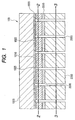
- a reference numeral 1000 denotes a compound semiconductor substrate
- a reference numeral 1009 denotes an etching stop layer
- a reference numeral 1010 denotes an etching sacrificial layer
- a reference numeral 1020 denotes a compound semiconductor multilayer film
- a reference numeral 1025 denotes a first groove
- a reference numeral 2000 denotes, for example, a silicon substrate.
- Reference numerals 2005, 2006, and 2010 denote a second groove, a third groove, and an insulating film (organic material film), respectively.
- a reference numeral 1000 denotes a first substrate (a compound semiconductor substrate or a substrate formed of, for example, Ge).
- a reference numeral 1009 denotes an etching stop layer
- a reference numeral 1010 denotes an etching sacrificial layer
- a reference numeral 1020 denotes a compound semiconductor multilayer film (here, details of the layer structure of the multilayer film are omitted).
- a reference numeral 1025 denotes a first groove for dividing the compound semiconductor multilayer film 1020 so as to be in an island shape on the compound semiconductor substrate.
- a reference numeral 1009 denotes an etching stop layer provided as necessary.
- a reference numeral 100 denotes a member according to the present invention.
- Reference numerals 2000, 2005, and 2010 denote a second substrate (for example, a silicon substrate), a second groove provided in the second substrate, and an insulating film (for example, an organic material film), respectively.
- the insulating film 2010 is also provided with a third groove 2006 connected to the second groove.
- the width and spacing of the first groove is shown equal to those of the second groove, the width of the first groove may be larger than that of the second groove.
- the width of an island of the compound semiconductor layer (the length in the direction of a short side described in the following) is smaller than the spacing between grooves passing through the second substrate.
- a silicon substrate is used as the second substrate, the second substrate is not limited specifically to a silicon substrate.
- the width of the first groove 1025 is, for example, from several micrometers to several hundred micrometers.
- the width of the second groove 2005 is, for example, from several micrometers to several hundred micrometers.
- the width is preferably 50 ⁇ m or more, more preferably 100 ⁇ m or more, and still more preferably 200 ⁇ m or more.
- the width of an island of the compound semiconductor layer is preferably smaller than the spacing between grooves passing through the silicon substrate.
- the insulating film 2010 may be omitted as appropriated.
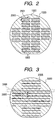
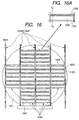
- Fig. 2 partially illustrates a section 2-2 in Fig. 1 .
- the compound semiconductor multilayer film 1020 is divided (patterned) in an island shape on the first substrate 1000.
- An island portion 1020 is in a projected form compared with portions surrounding it.
- the compound semiconductor multilayer film 1020 is patterned in a desired shape, and it is not necessarily required to be in a rectangular island shape as illustrated in the figure.
- the direction of a long side of a rectangular island is sometimes referred to a longitudinal direction while the direction of a short side is sometimes referred to as a traversal direction.
- like reference numerals designate like members in Fig. 1 , and the same applies to drawings referred to in the following.
- the first groove 1025 is a space (a gap) in the island-shaped compound semiconductor multilayer film 1020. It is to be noted that like reference numerals designate like structural members in Fig. 1 .
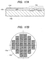
- Fig. 3 illustrates a section 3-3 in Fig. 1 .
- the second groove 2005 is provided in the second substrate 2000. It is to be noted that the second groove 2005 is intermittently formed. By intermittently providing the passing-through groove in this way, in the case of, for example, a silicon wafer, the stiffness thereof is not considerably lost, and thus, a situation that handling thereof in subsequent processes becomes difficult can be avoided.
- the passing-through groove is preferably formed separately (intermittently) with the longitudinal direction of the second groove (passing-through groove) being along a chip scribe line which is used when the wafer is separated into chips in a downstream process, taking into consideration the mechanical strength.
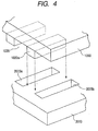
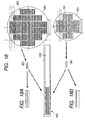
- Fig. 4 is a partially exploded perspective view illustrating a positional relationship between the first groove 1025 and a semiconductor substrate groove 2005 and illustrating a state where an island-shaped compound semiconductor multilayer film 1020 is disposed between the semiconductor substrate grooves 2005. It is to be noted that, in Fig. 4 , the insulating film 2010, the etching stop layer 1009, and the etching sacrificial layer 1010 are omitted for the sake of simplification.
- an island 1020a in the projected form is located right between passing-through grooves 2005a and 2005b.
- the passing-through groove 2005 is not necessarily required to be provided so as to be located in parallel with the longitudinal direction of the patterned compound semiconductor multilayer film 1020 as illustrated in Figs. 2 and 3 .
- the passing-through groove 2005 may be provided so as to be perpendicular to or so as to intersect with the longitudinal direction.
- the passing-through groove may also be referred to as a passing-through hole because it passes through the substrate.
- the member 100 is prepared which is formed so as to include the first substrate (for example, a compound semiconductor substrate) 1000, the etching sacrificial layer 1010, the compound semiconductor multilayer film 1020, the insulating film (for example, an organic insulating material film) 2010, and the second substrate (for example, a silicon substrate) 2000.
- the first substrate for example, a compound semiconductor substrate
- the etching sacrificial layer 1010 for example, the compound semiconductor multilayer film 1020
- the insulating film for example, an organic insulating material film
- the second substrate for example, a silicon substrate 2000.
- the etching stop layer 1009 may be provided as necessary and is not essential.
- an etchant is made to penetrate into the member through the second groove 2005 and the third groove 2006 which pass through the second substrate 2000 (for example, a silicon substrate) and the insulating film 2010, respectively.
- etching is carried out to separate the first substrate 1000 from the member.
- the first groove 1025 passes through the etching sacrificial layer 1010, the first groove 1025 is not required to pass through the etching sacrificial layer 1010. What is necessary is that the etching sacrificial layer can be exposed when or before the first substrate 1000 is removed from the member 100.
- the etching stop layer 1009 illustrated in Fig. 1 may be provided as necessary.
- the etching stop layer is not necessarily required to be provided. However, this layer has the effect of uniformly exposing the etching sacrificial layer over the whole wafer.
- the member may be, for example, prepared according to the following two methods.
- the present invention is not limited to the following two methods.
- a first method is implemented so as to include the following steps A1) to E1):
- the patterning is carried out such that, for example, as illustrated in Fig. 2 , the island in the projected form remains.
- the first groove may extend in the direction of the etching sacrificial layer and the etching sacrificial layer immediately below the first groove may be completely removed.
- regions below the etching sacrificial layer for example, the first substrate, the etching stop layer, and/or a buffer layer
- the third groove may be provided after the step E1 which is a bonding process.
- the order of the above steps is not limited to the one specified in the above.
- the step D1) may be carried out before the steps A1) to C1).
- the controllability is further enhanced if the etching stop layer is epitaxially grown on the compound semiconductor substrate before the etching sacrificial layer is epitaxially grown. More specifically, the uniformity of the etching over the whole substrate is improved. Although the etching stop layer is formed as shown in Fig. 1 , such layer is not essential for the present invention.
- the spacing of the second passing-through grooves 2005 formed in the second substrate 2000 such as a silicon substrate and the width of the compound semiconductor multilayer film separated in an island shape are substantially equal or the width of the compound semiconductor multilayer film is smaller.
- the second groove 2005 is formed by dry etching (RIE) or the like, for example, halfway in the depth direction of the second groove illustrated in Fig. 1 (in the figure, the depth direction is the upward direction), that is, such that the material forming the second substrate is partly left on the side of the insulating film 2010.
- RIE dry etching
- the mask used in RIE is not specifically limited, and is, for example, SiN.
- the first substrate 1000 is bonded to the second substrate.
- the groove formed in the second substrate may be extended in the depth direction by wet etching or the like such that the groove passes through the second substrate 2000.
- the second groove 2005 is formed by dry etching (RIE) or the like, for example, halfway in the depth direction of the second groove illustrated in Fig. 1 (in the figure, the depth direction is the leftward direction), that is, such that the material forming the second substrate is partly left on the side of the insulating film 2010. Then, after the groove formed in the second substrate is extended by wet etching or the like such that the groove passes through the second substrate 2000, the first substrate 1000 may be bonded to the second substrate.
- RIE dry etching
- the insulating film 2010 is provided on the second substrate, it is also acceptable that, after the insulating film is provided on the compound semiconductor multilayer film 1020 which is patterned in a desired shape, it is bonded to the second substrate.
- the second substrate is a silicon substrate or a substrate having a silicon region
- an oxide layer formed on the surface may be used as the insulating film.
- the insulating film 2010 disposed in the member 100 may be provided in advance on the side of the first substrate, on the side of the second substrate, or on the side of both the first and the second substrates. It is to be noted that the insulating film 2010 may be omitted when, for example, the second substrate is an insulating substrate such as a quartz and glass substrate.
- a second method of preparing the member is carried out according to the following steps:
- the second groove 2005 is formed by dry etching (RIE) or the like, for example, halfway in the depth direction of the second groove illustrated in Fig. 1 (in the figure, the depth direction is the leftward direction), that is, such that the material forming the second substrate is partly left on the side of the insulating film 2010.
- RIE dry etching
- the present invention does not exclude presence of another layer, film, or region between the structural substrates, structural layers, or structural films, or does not exclude film formation or bonding which includes such presence.
- a metal film may be partly or wholly provided between the insulating film 2010 and the second substrate 2000, and a wiring region or a circuit region may be provided on the second substrate or may be provided using the second substrate and the insulating film.
- the circuit region referred to herein is a driving circuit or a switching circuit when a light-emitting device or a light-receiving device is manufactured using the compound semiconductor multilayer film, or a circuit including wiring just for energization or voltage application.
- the second substrate 2000 includes, for example, a semiconductor substrate, a silicon substrate, a silicon wafer having an oxide layer formed on the surface thereof, and a silicon wafer having a desired electric circuit (for example, a driver) provided thereon.
- a silicon substrate having an insulating film as illustrated in Fig. 1 is formed, for example, as in the following.
- a mask layer for forming the second groove 2005 as a semiconductor substrate groove is formed on the other surface using a resist, and the semiconductor substrate groove 2005 is formed in the silicon substrate using the mask. Dry etching such as RIE or wet etching may be used. A sandblaster for forming a groove by causing quartz particles or the like to collide with the exposed portions to physically break the silicon substrate may also be used. Of course, combinations thereof may also be used.
- a groove may be formed to some extent in the depth direction by RIE or a sandblaster, and after that, a passing-through hole may be formed in the first substrate formed of silicon or the like by wet etching before (or after) bonding to the first substrate.
- the groove may also be exposed by grinding or abrasion from the rear surface of the first substrate.
- the second groove 2005 which passes through the silicon substrate is formed.
- an organic material film for example, a positive type photosensitive polyimide film
- UV light is applied from the side of the other surface with the silicon substrate being the mask.
- only the portion of the organic material film located above the second groove 2005 is developed and removed.
- the step of exposing the organic material film by using the silicon substrate having the passing-through groove therethrough as the mask and removing the exposed organic material film may be carried out with the first substrate being bonded to the silicon substrate.
- UV light may be applied from the side of the second substrate and the organic material film immediately above the second groove may be removed to form the third groove.
- the method of manufacturing the passing-through grooves formed in the silicon substrate and in the insulating film is not specifically limited, and imprinting using a mold (stamper) having a predetermined pattern may also be used.
- the passing-through groove may be formed not by chemical etching but by fluid energy or by causing solid particles to collide such as sandblasting.
- a driver circuit may be provided in the silicon substrate 2000.
- the driver circuit referred to herein is, for example, a circuit for driving and controlling the LED, when a light-emitting diode (LED) is formed so as to include the compound semiconductor multilayer film.
- LED light-emitting diode
- the silicon substrate a so-called CZ wafer
- the silicon substrate may be, of course, a substrate having an epitaxial silicon layer on the surface thereof.
- an SOI substrate may be used instead of the silicon substrate.
- the surface of side walls of the passing-through groove in the silicon substrate may be treated using ozone ashing or a piranha solution which is a mixture of sulfuric acid and hydrogen peroxide.
- a metal film may exist therebetween or between the insulating film on the silicon substrate and the first substrate. It can function as a reflection layer when an LED device is manufactured.
- a DBR mirror may be used instead of the metal film.
- the metal film for example, Ti, Au, or Pt
- the metal film may also be provided between the insulating film and the second substrate (for example, silicon).
- the DBR layer is disposed between the compound semiconductor multilayer film 1020 and the insulating film 2010.
- the second substrate other than the silicon substrate, a glass substrate, a quartz substrate, a metal substrate, a ceramic substrate, a substrate coated with an insulating film, or the like may be applied.
- the thickness of the second substrate is not specified, such a thickness as 525 ⁇ m (4 inches), 625 ⁇ m (6 inches), 725 ⁇ m (8 inches), or 775 ⁇ m (12 inches) may be used.
- the thickness of the second substrate is, for example, in the range of 300 ⁇ m to 1000 ⁇ m, and, from the viewpoint of securing the strength and from the process viewpoint, preferably in the range of 400 ⁇ m to 800 ⁇ m.
- the passing-through groove (passing-through hole) in the second substrate may be a rectangular slit, or may be slits which are intermittently disposed at specified intervals as illustrated in Fig. 3 .
- Die Bonding Film (Hitachi Chemical Co., Ltd.) may be used to bond the first substrate to the second substrate.
- the Die Bonding Film manufactured by Hitachi Chemical Co., Ltd. which functions both as a dicing tape and a die bonding film is bonded onto the second substrate such as a silicon substrate to improve the handleability. After that, alignment and the like are performed.
- the dicing tape is removed (for example, removed by UV light application) and bonding to the side of the first substrate is performed. It is to be noted that, when the die bonding film remains on the second groove which passes through the second substrate, it is removed by etching or the like and coupling to the first groove is performed.
- the passing-through grooves formed in the second substrate are preferably a plurality of passing-through grooves in the shape of rectangles (strips) having a long side and a short side or of quadrilaterals which are intermittently provided.
- the plurality of passing-through grooves are aligned (in arrays) and intermittently disposed in the direction of the long side (in the longitudinal direction) of the passing-through grooves.
- “intermittently” means that there is a gap between the grooves, that is, the grooves are separated. This is preferable also from the viewpoint of securing the strength of the substrate which is important when the substrate is introduced into a subsequent device process.
- the width of the gap is, for example, in the range of several micrometers to several hundred micrometers.
- the grooves which are intermittently provided in arrays are provided such that the grooves in the arrays are in parallel with one another as illustrated in Fig. 3 .
- a GaAs substrate As the first substrate 1000, a GaAs substrate, a p-type GaAs substrate, an n-type GaAs substrate, an InP substrate, an SiC substrate, a GaN substrate, or the like may be applied. It is to be noted that, other than a compound semiconductor substrate, a sapphire substrate or a Ge substrate may be used. A compound semiconductor substrate such as a GaAs substrate or a GaN substrate is preferable.
- the etching sacrificial layer referred to here is a layer which is etched faster than the compound semiconductor multilayer film, and it can be also referred to as a separation layer.
- the etching rate ratio of the etching sacrificial layer to the multilayer film thereon is five or more, preferably ten or more, and more preferably 100 or more.
- the etching sacrificial layer is, for example, an AlAs layer or an AlGaAs layer (for example, Al 0.7 Ga 0.3 As).
- the etching selectivity becomes remarkable when x is 0.7 or more.
- a diluted solution of 2-10% HF may be used as the etchant.
- the etchant is, for example, 10% hydrofluoric acid.
- a sapphire substrate may be used as the first substrate and a metal nitride film such as chromium nitride (CrN) may be used as the etching sacrificial layer thereon.
- CrN chromium nitride
- a multilayer film as a functional layer for materializing a device (an LED or a laser) for blue or UV light is epitaxially grown on the chromium nitride.
- GaInN as an active layer and, further, AlGaN or GaN as a spacer layer may be used.
- a common Cr etchant (a chromium etchant) may be used as the etchant of the sacrificial layer.
- a common Cr etchant (a chromium etchant) may be used as the etchant of the sacrificial layer.
- Such an etchant is supplied by Mitsubishi Chemical Corporation.
- the passing-through groove may be manufactured by RIE (reactive ion etching) using fluorine under an atmosphere of SF 6 or the like.
- RIE reactive ion etching
- fluorine a radical species
- the radical species is not limited to fluorine.
- wet etching NaOH, KOH, TMAH, or the like may be used.
- the etching sacrificial layer may be exposed at any point of time.
- the passing-through groove may be formed in the silicon substrate by RIE (reactive ion etching).
- RIE reactive ion etching
- a mixture of an oxidant such as HNO 3 and a hydrogen fluoride solution may be used as the etchant using the fact that a silicon oxide is dissolved in hydrofluoric acid.
- CH 3 COOH, Br 2 , or the like is used as an additive (Multiple Epitaxial Layer).
- the etching sacrificial layer 1010 and the compound semiconductor multilayer film 1020 may be alternately repeatedly laminated on the first substrate 1000.
- the compound semiconductor multilayer film can be repeatedly transferred onto the silicon substrate.
- the etching stop layer 1009, the etching sacrificial layer 1010, and the compound semiconductor multilayer film 1020 may also be alternately repeatedly laminated.
- the alternate and repeated lamination on the first substrate in advance can avoid a plurality of times of thermal hysteresis for the epitaxial growth on the substrate even when the transfer of a pair of a sacrificial layer and a multi-layer 1020 is carried out a plurality of times one by one, which is preferable.
- the plurality of times of uses of the substrate is expected to have remarkable economic effects, because, generally speaking, a compound semiconductor substrate is ten times or more as expensive as silicon.
- the layer structure and material of the compound semiconductor multilayer film depend on what device is provided as a semiconductor article.
- Exemplary semiconductor articles as light-emitting devices include a light-emitting diode device (an LED device), a light-emitting laser diode (an LD device), and a light-receiving device.
- the layer structure uses the following materials.
- a p-AlAs layer (an etching sacrificial layer) is formed on a p-type GaAs substrate, and the following layers are provided thereon as the compound semiconductor multilayer film.
- a p-type GaAs contact layer, a p-type AlGaAs clad layer, a p-type AlGaAs active layer, an n-type AlGaAs clad layer, and an n-type GaAs contact layer are provided.
- GaInP may be used between the sacrificial layer and the compound semiconductor substrate.
- the GaAs layer and the AlGaAs layer are etched with sulfuric acid, the etching is stopped by the GaInP layer. After that, the GaInP layer is removed by hydrochloric acid.
- AlAs is desirable as the stop layer.
- compound semiconductor materials other than GaAs for example, AlGaInP type, InGaAsP type, GaN type, AlGaN type, and InAlGaN type can be applied to the present embodiment.
- At least one of a metal film and a DBR mirror may be provided between the compound semiconductor multilayer film 1020 and the insulating film 2010 formed of the organic material or the like.
- the metal film is formed of, for example, Au, Ag, Ti, Al, or AlSi, or a multilayer film formed of these materials.
- a preferable metal film material is selected according to a wavelength of light to be emitted by the LED. For example, when a red LED of 700-800 nm is to be manufactured, Au, Ag, or the like has a high reflectance. In case of a blue LED of about 360 nm, Al is preferable.
- a DBR mirror (Bragg Reflector) is formed by, when it is for a GaAs compound semiconductor material, alternately laminating an AlAs layer and an AlGaAs layer a plurality of times or alternately laminating an Al oxide layer and an Al 0.2 Ga 0.8 As layer. Because it is difficult to form an aluminum oxide by epitaxial growth, actually, it is preferable to control the index of refraction by, for example, alternately switching the value of x between 0.2 and 0.8 in Al x Ga 1-x As. Of course, by making higher the composition ratio of Al in the layer on the side of the lower index of refraction and by its oxidation after the lamination, Al oxide may be formed.
- a homojunction LED as described in Japanese Patent Laid-Open Application No. 2005-012034 may be formed.
- an impurity is diffused by solid phase diffusion to form a pn junction in the active layer.
- the contact layer forms an ohmic contact with a p-type electrode or an n-type electrode
- an impurity concentration which is higher than that of the clad layers sandwiching the active layer is preferable.
- the spacing of patterned island-shaped regions on the first substrate in the direction of the long side of the rectangular shape substantially corresponds to the spacing for dicing in a subsequent process.
- a reference numeral 2901 in Fig. 2 denotes the direction of the long side while a reference numeral 2902 denotes the direction of the short side.
- etching sacrificial layer is removed from the member
- further device separation may be carried out such that dot-like light emitting points are formed in the compound semiconductor multilayer film using a mask or the like.
- the insulating film 2010 is, for example, a film formed of an organic material.
- a film formed of an organic material is, for example, a polyimide or other organic insulating film, or an insulating film.
- a film formed of an organic material includes an organic insulating film such as polyimide.
- the insulating film is formed of a positive type photosensitive polyimide.
- the exposed portion substantially does not have further photosensitivity.
- not only a positive type photosensitive polyimide but also a negative type photosensitive polyimide and even a nonphotosensitive polyimide can be applied to the present invention as long as a third passing-through groove can be formed using another mask or the like.
- such a polyimide is supplied by, for example, HD Micro Systems, Ltd.
- Japanese Patent Laid-Open Application No. 2005-012034 describes in detail a photosensitive polyimide. More specifically, an aromatic anhydride reacts with an alcohol having a double bond (for example, hydroxyethyl methacrylate) to form a dicarboxylic acid, which reacts with a diamine to form a polyamide having a double bond on a side chain thereof. This corresponds to a structure where a carboxyl group of a polyamic acid is substituted by a structure having a polymerizable double bond.
- a solution where the polymer is dissolved in a polar solvent such as NMP (n-methyl pyrrolidone) together with a photoinitiator, a sensitizer, an adhesive aid, and the like is the photosensitive polyimide.
- a photosensitive or nonphotosensitive polyimide may be used as the polyimide.
- organic material films can be used for bonding the compound semiconductor substrate to the silicon substrate.
- an epoxy adhesive layer or the like can be adopted.
- the organic insulating layer above the passing-through groove in the silicon can be removed in a self-aligning manner.
- the insulating film not only the organic material film described in the above but also an inorganic insulating oxide film such as a silicon oxide film may be used. Further, a siloxane resin or the like may also be used.
- spin on glass may be used to form a silicon oxide insulating film in order to enhance the planarity of the circuit region.
- SOG spin on glass
- a plurality of kinds of insulating films may be laminated to be used.
- the insulating film may be formed using an organic material such as a polyimide.
- an organic material such as a polyimide.
- the insulating film may be omitted as necessary. Further, the insulating film may be formed of a plurality of layers. An insulating film may be provided on each of the side of the first substrate and the side of the second substrate for bonding, or, the insulating film may be provided on the side of only one of the substrates.
- the insulating film 2010 may be omitted.
- a photosensitive polymer sheet may be used as the insulating film. More preferably, the polymer sheet as itself has adhesion ability. It is to be noted that, when the insulating film is formed on the second substrate or when the insulating film is formed on the side of the first substrate, it may be formed after heating and pressure-bonding processes. Of course, a dilute organic material (photosensitive polyimide or the like) may be formed into a film by spin coating. Or, a photosensitive polyimide sheet which is a photosensitive polyimide formed to be sheet-like such as a dry film may be used.
- An exemplary semiconductor article manufacturing method is described in the following. More specifically, the method is implemented so as to include the following steps:
- the manufacturing method is described in detail in an example described in the following. It is to be noted that, in the process 2), the present invention does not exclude inclusion of a layer other than the described layers, and presence of a material other than the layers and films described in the above is of course within the scope of the present invention.
- the member formed by the bonding according to the present invention has the following characteristics.
- a semiconductor member having a compound semiconductor multilayer film on a silicon substrate includes an AlAs layer, a compound semiconductor multilayer film, an organic insulating film, and a silicon substrate on the compound semiconductor substrate in the stated order from the side of the compound semiconductor substrate, the compound semiconductor multilayer film being provided with a first groove such that the sacrificial layer is exposed, and the silicon substrate and the organic material film being provided with a second groove connected to the first groove.
- bubbles of gas (hydrogen) generated by etching the etching sacrificial layer formed of AlAs or the like may block an exit of the grooves.
- ultrasound intermittent application is also applicable
- alcohol for example, to the hydrofluoric acid.
- At least one of a metal film or a DBR mirror may be provided between the compound semiconductor light-emitting layer and the insulating film such as an organic material film.
- the insulating film such as an organic material film.
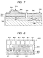
- the mirror when the mirror is a mirror formed of Ti, Au, Pt, AlSi, or the like, the mirror may be between the organic material film and the second substrate as illustrated in, for example, Fig. 7 .
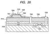
- a reference numeral 7010 denotes an insulating layer and a reference numeral 7081 denotes a mirror and the details are described in the following.
- the DBR mirror may be continuously epitaxially grown on the compound semiconductor layer which is epitaxially grown.
- a reference numeral 7021 in Fig. 20 is the mirror layer. The details are described in the following.
- a metal mirror may be formed by deposition above the grown compound semiconductor multilayer film, may be formed by deposition above the organic insulating layer, or the both may be simultaneously formed.
- the DBR as the mirror is described in detail in the following.
- the DBR layer forms a light-emitting layer which is formed on the first substrate via the etching sacrificial layer (separation layer) so as to include the active layer.
- the first substrate is a substrate for forming an LED (a light-emitting diode).
- a substrate on which a compound semiconductor film for an LED can be grown is used.
- Exemplary materials for the first substrate include, when an III-V compound which is basically GaAs is grown, a GaAs substrate and a Ge substrate the lattice constant of which is close to that of GaAs.
- the substrate may include Al, P, or the like which are elements of the same group.
- an impurity for forming a p-type or an n-type may be included.
- the sacrificial layer, the light-emitting layer, and the DBR layer are epitaxially grown on the first substrate in sequence by MOCVD, MBE, or the like.
- the sacrificial layer is a layer formed of a material which can be selectively etched in relation to the light-emitting layer, and is formed of, for example, AlAs or Al x Ga 1-x As (1 ⁇ x ⁇ 0.7).
- the sacrificial layer of such composition is selectively etched with a hydrofluoric acid solution.
- the light-emitting layer is formed of a compound semiconductor layer which functions as a light-emitting device, and, for example, GaAs, AlGaAs, InGaAs, GaP, InGaP, AlInGaP, and the like can be used. There is a pn junction in the layer. Further, as a specific structure, the light-emitting layer 1102 is formed of, for example, an active layer sandwiched between clad layers.
- the DBR layer can be epitaxially grown on the first substrate, and has a structure where a plurality of pairs each having layers of different indices of refraction with regard to the target LED wavelength are laminated.
- Each of the pairs is formed of a high refractive index layer and a low refractive index layer. That formed by laminating the pair a plurality of times is referred to as a Bragg reflector film or a DBR mirror (DBR layer).
- a Bragg reflector film or a DBR mirror (DBR layer).
- the Bragg reflector film obtains a reflectivity which corresponds to the number m of the pairs by setting the film thicknesses d1 and d2 of the two kinds of films having different indices of refraction such that the optical film thickness n ⁇ d is 1/4 of the wavelength and preparing m pairs of the two kinds of films (m is a natural number which is equal to or larger than two).
- m is a natural number which is equal to or larger than two.
- the conditions for forming the DBR are optimized such that a light of a specific wavelength can be reflected with the efficiency of 70% or more, preferably 80% or more, and more preferably 90% or more.
- the DBR layer is obtained by alternately laminating AlGaAs layers containing different amount of Al.
- the amount x of Al which is contained in the layer is 0.8 or less when the material is expressed as Al x Ga 1-x As.
- the amount x is preferably 0.7 or less, more preferably 0.6 or less, and still more preferably 0.4 or less.
- the lower limit of x is, for example, zero.
- the low refractive index layer which forms the DBR layer and the index of refraction of which is lower than the other layer is selected from the group consisting of Al x Ga 1-x As (0 ⁇ x ⁇ 0.8), an AlInGaP type material, and an AlGaP type material. It is important that the etching sacrificial layer is selected from the group consisting of AlAs and Al x Ga 1-x As (0.7 ⁇ x ⁇ 1.0) and the combination of the materials is such that the low refractive index layer is resistant to damage when the separation layer is selectively etched and removed.
- the separation layer may be selectively removed without greatly depending on the amount of Al contained.
- a p-AlAs layer as a separation layer of a thickness of 100 nm, a light-emitting layer of a thickness of about 2000 nm, and an n-DBR layer are grown on a 4-inch GaAs substrate 100 by MOCVD.
- the details of the light-emitting layer are as follows. It is formed of p-Al 0.4 Ga 0.6 As: 350 nm as a clad layer, pAl 0.13 Ga 0.87 As: 300 nm as an active layer, and n-Al 0.23 Ga 0.77 As: 1300 nm to be a clad located on the side of the DBR layer.
- n-DBR layer it can be formed by laminating 20 pairs of Al 0.2 Ga 0.8 As: 63.3 nm / Al 0.8 Ga 0.2 As: 56.5 nm. It is to be noted that, by making lower the resistivity of the materials forming the DBR, electrical connection can be secured from the DBR mirror denoted as 7021 in Fig. 20 .
- GaInP when used as the etching sacrificial layer, which is not necessarily required in the present invention, GaInP, for example, can be used as an etching stop layer.
- a buffer layer before the etching sacrificial layer is grown on the first substrate for example, a compound semiconductor substrate such as a GaAs substrate, a Ge substrate, or a GaN substrate, a satisfactory epitaxial layer with a small number of defects can be obtained.
- a GaAs thin film as the buffer layer can be formed on the GaAs substrate.
- GaInAs or the like is suitable for lattice strain relaxation.
- the alignment between the first substrate and the second substrate can be performed using a double-sided aligner used for wafer bonding or the like.
- the second substrate is a silicon substrate
- the passing-through groove provided in the substrate may be used as an alignment mark.
- the passing-through groove may be formed on a scribe line.
- the light-emitting layer transferred onto the silicon has an area as large as several hundred microns which corresponds to a chip size, and device separation of individual light-emitting devices of several ten microns and the like are fixed in a process after the transfer.
- bonding the island-shaped active layer to the passing-through groove does not require the accuracy of several microns which is required in a device process, and an accuracy of several ten microns is satisfactory. From this viewpoint, an orientation flat of a wafer may be used as the standard of the alignment.
- the bonding is easily carried out by heating to a temperature of several hundred degrees or higher which is the glass transition temperature of the organic insulating layer as the insulating film 2010 in Fig. 1 to give tackiness thereto and by press bonding the silicon wafer.
- the bonding strength is satisfactory with no problem in subsequent processes.
- a void which is liable to occur in direct bonding without using an adhesive layer and without tackiness is separated in an island shape and the active layer exists. Therefore, intake of air easily disappears along the separation groove between the islands in pressure bonding. Bonding under a reduced pressure decreases the amount of the void itself, and thus, formation of the gap itself is drastically reduced.
- an etchant bath may be disposed in a vacuum to soak the member in the etchant under a reduced pressure such that the etchant penetrates into the sacrificial layer more uniformly through the passing-through groove.
- vibration by ultrasound, heating, and rotational motion such as axial revolution and orbital revolution of the wafer itself increase liquid circulation speed to complete the transfer and separating processes uniformly in a short time.
- a method of forming a compound semiconductor multilayer film on a first substrate such as GaAs via an etching sacrificial layer (also referred to as a separation layer) and forming a pair formed of the two layers a plurality of times such that decreasing the cost of the process can be expected is described.
- a reference numeral 1000 denotes a first substrate (for example, GaAs), and a reference numeral 2101 denotes a buffer layer.
- a substrate on which such layers can be epitaxially grown is the first substrate.
- Exemplary substrates include a GaAs substrate and a Ge substrate the crystal lattice constants of which are close to that of AlAs (AlGaAs).
- AlGaAs AlAs
- the lattice constant of Si is different from that of GaAs by about 4%, it is possible to directly grow GaAs on Si. Therefore, it is also possible to use an Si substrate having a GaAs film grown thereon as the first substrate 1000. Further, an impurity may be doped in these substrates.
- the separation layer 2102 and a light-emitting layer 2103 including an active layer are epitaxially grown on the first substrate 1000 in sequence.
- the material of the separation layer 2102 is AlAs or Al (x) Ga (1-x) As(x ⁇ 0.7), and the film thickness is preferably several ten to several hundred nanometers.
- the light-emitting layer 2103 is a compound semiconductor multilayer film as a light-emitting device, and, for example, GaAs, AlGaAs, InGaAs, GaP, InGaP, or AlInGaP is used. There is a pn junction in the light-emitting layer 2103.
- buffer layer 2101 is formed prior to formation of the separation layer 2102, this is arbitrary.
- the object of the buffer layer 2101 is to decrease crystal defects and the like.
- the growth method is not specifically limited, and any of MOCVD, MBE, LPE, and the like may be used.
- the separation layer 2102 and the light-emitting layer 2103 are paired, and a plurality of pairs of separation layers 3102 and 4102 and light-emitting layers 3103 and 4103 are grown in sequence such that the number of the pairs reaches n.
- a light reflection layer 4104 is formed on the uppermost light-emitting layer 4103.
- a resist patterning 2105 is formed so as to leave the light reflection layer 4104 in an island shape.
- the material of the light reflection layer 4104 is preferably a material having a high reflectivity with respect to the wavelength of a light-emitting device to be formed.
- a material having a high reflectivity with respect to the wavelength of a light-emitting device to be formed For example, when the material of the light-emitting device is of the GaAs type and the light-emitting wavelength is about 750-800 nm, Au (gold), Ag (silver), Al (aluminum), and.the like are preferable. Of course, other light-reflecting materials may be used.
- the material of the light reflection layer 4104 is preferably Al or the like. It is to be noted that the DBR layer described in the above may be used instead of the light reflection layer, and it may be possible that no specific light reflection layer is provided. In other words, the light reflection layer 4104 may be omitted.
- the light-emitting layer 4103 in an island shape may form a light-emitting layer of one light-emitting device or may be a region where a plurality of light-emitting devices are included in an array.
- the size of the island-shaped light-emitting layer 4103 is in agreement with the chip size when the second substrate 2000 to be described below is diced.
- the light reflection layer 4104 is not essential. It may be formed on the side of the second substrate 2000 described in the following, or it may be completely omitted.
- the light reflection layer 4104 and the uppermost light-emitting layer 4103 are etched in an island shape to expose part of the uppermost separation layer 2102. It is to be noted that the above-described first groove surrounds the light-emitting layer such that the light-emitting layer is in an island shape.
- the first substrate 1000 is bonded to the second substrate 2000.
- the material of the second substrate 2000 is arbitrary, and any material may be used including a semiconductor substrate such as an Si substrate, a conductive substrate, and an insulating substrate. As described in the above, a driver circuit for driving the light-emitting layer and the like may be provided. Further, an insulating film such as an organic material film may be provided on the surface.
- a light reflection layer 4104 may be formed on the surface of the second substrate 2000. Further, the reflection layer 4104 may be formed on the surfaces of the first substrate 1000 and of the second substrate 2000 or the reflection layers 4104 may be bonded to each other.
- bonding the first substrate 1000 to the second substrate 2000 As the method of bonding the first substrate 1000 to the second substrate 2000, heating after bonding, pressurizing, using the both, and the like may be used. Bonding in an atmosphere under a reduced pressure is also effective.
- space 2106 made by the patterned groove is formed in proximity to the interface.
- the first groove and the second groove are connected to the space 2106.
- Fig. 21E is a view illustrating a state where the substrates are separated.
- the separation is achieved by etching the separation layer 4102 which is the uppermost layer.
- the etchant flows into the space 2106 formed by the island-shaped separation region.
- the separation layer 4102 which is the uppermost layer is etched, and, as a result, the first substrate 1000 and the second substrate 2000 are separated.
- a hydrofluoric acid solution, a hydrochloric acid solution, or the like may be used as the etchant used here.
- the light-emitting layer 4103 in the island-shaped region is transferred onto the second substrate 2000.
- the second substrate 2000 onto which the light-emitting layer 4103 is transferred proceeds to the device process, and a light-emitting device is formed.
- the surface of the first substrate 1000 which lost the uppermost light-emitting layer 4103 and the uppermost separation layer 4102 due to the transfer and etching becomes the light-emitting layer 4103, and the process returns to the one illustrated in Fig. 21A .
- the light-emitting layer 4103 and the separation layer 4102 are paired, by repeating n times the above-described process in which n is the number of times the pair is formed, substrates for forming n light-emitting devices can be formed. It is to be noted that, although a case where the separation layer and the light-emitting layer are paired is described, the reflection layer may be added to the pair to form a set of the three layers and the set may be laminated a plurality of times.
- a novel semiconductor article manufacturing method and a novel member are provided.
- a light-emitting device typically an LED
- a device separating process, a wiring process, a process for dicing the second substrate, and the like are appropriately performed.
- the device separation for manufacturing an LED having a plurality of light emitting points on a chip for example, when the conductivity type of the front surface side of the compound semiconductor multilayer film is p, patterning is carried out to an n-type layer below that or nearly to the active layer to remove them. In this way, the device separation can be carried out.
- the direction of the dicing and the second passing-through groove may be opposite to those in the case illustrated in Fig. 3 . More specifically, not the passing-through groove along the direction of the long side of the chip as illustrated in Fig. 3 but a passing-through groove perpendicular thereto is provided along the direction of the short side.
- a passing-through groove perpendicular thereto is provided along the direction of the short side.
- the space between chips has a side surface formed not by dicing but by a passing-through groove (manufactured by, for example, RIE) provided in advance. This is preferable taking into consideration a case where dense arrangement is made.
- a passing-through groove along the direction of the long side and a passing-through groove along the direction of the short side are intermittently provided below the island-shaped compound semiconductor multilayer film.
- Fig. 6 is a sectional view illustrating an exemplary structure where a driving circuit and an LED array are connected on a wiring substrate.
- the LED array can be obtained by, in the process (7) of the above-described semiconductor article manufacturing method, forming a plurality of LED devices on an island-shaped compound semiconductor multilayer film on a silicon substrate and dividing the silicon substrate by dicing.
- the cross sectional structure of the respective LED devices is the same as LED devices including an LED light emitting region on the left in Fig. 7 and Fig. 15 described in the following.
- Fig. 6 is a sectional view illustrating an exemplary structure where a driving circuit and an LED array are connected on a wiring substrate.
- the LED array can be obtained by, in the process (7) of the above-described semiconductor article manufacturing method, forming a plurality of LED devices on an island-shaped compound semiconductor multilayer film on a silicon substrate and dividing the silicon substrate by dicing.
- the cross sectional structure of the respective LED devices is the same as LED devices including an LED
- a plurality of LED array chips 4000 are arranged on a wiring substrate 5000 in a line, and a plurality of driver ICs 3050 similarly arranged in a line on both sides of the plurality of LED array chips 4000, and the LED array 4000 are electrically connected with the plurality of driver ICs 3050 by wire bonding.
- the respective LED devices of the LED array chips 4000 are electrically connected with drive devices of the driver ICs 3050 alternately arranged on both sides of the LED array chips 4000 by wire bonding.
- the plurality of driver ICs 3050 are arranged in a line on both sides of the plurality of LED array chips 4000 disposed in a line.
- the plurality of driver ICs 3050 may be arranged on one side of the plurality of LED array chips 4000.
- an LED printer head ( Fig. 5 ) may be formed. Light emitted from the LED array 4000 disposed in a line is collected by the rod lens array 3000 to obtain an LED array image 3060.
- a rod lens array for example, an SLA: Selfoc Lens Array
- an LED device forming layer is provided on the silicon substrate via a metal film or a DBR mirror, by improving the directivity and increasing the brightness, a device light emitting point having enough brightness is materialized even if the device dimension is one obtained by microfabrication. Therefore, it is possible to omit the rod lens array and to directly form a latent image on a photosensitive member directly from an LED printhead, and the LED printer head having the structure illustrated in Fig. 5 the number of parts of which is small and the economic effect of which is great may be formed.
- Fig. 6 illustrates a case where the driver ICs (driving circuit) and the LED devices are connected with each other by wire bonding
- the driver circuit may be directly built on the side of the Si substrate to be connected with the LED devices ( Fig. 7 in which a reflection layer is provided on an organic insulating layer immediately below a device).
- an insulating film 7010 formed of an organic material is provided on a silicon substrate 7000 including a MOS transistor 7060 which forms a driver IC. Then, an LED light emitting region 7070 formed of a compound semiconductor multilayer film is provided on the insulating film 7010.
- a reference numeral 7080 denotes an insulating film (such as SiO 2 or SiN) and a reference numeral 7050 denotes a wire pad to be a source or drain region of the MOS transistor 7060.
- a reference numeral 7081 denotes a layer which functions as a mirror (for example, a metal mirror of Ti, Au, or the like) and reference numerals 7083 and 7084 denote wiring, embedded wiring, or an electrode pad.
- a chip 1960 illustrated in Fig. 19 can be cut out by dicing in a dicing direction 1625.
- Fig. 19 illustrates a state where the cut chip arrays 1960, an enlarged view of which is shown in Fig. 19A , are arranged on a print substrate 1930.
- a reference numeral 1911 denotes a second substrate. It is to be noted that, although a second groove which is a passing-through groove is intermittently provided in the second substrate along the long side of the chip as illustrated in Fig. 3 , it is omitted in Fig. 19 .
- Fig. 8 illustrates an exemplary matrix drive.
- Fig. 8 is a view illustrating a light-emitting device array circuit 8500 which can be time-division driven for decreasing the number of electrodes.
- a reference numeral 8011 denotes an n-side electrode
- a reference numeral 8017 denotes a p-type electrode
- a reference numeral 8021 denotes an insulating film on n-type AlGaAs
- a reference numeral 8022 denotes an insulating film on a p-type GaAs contact layer
- a reference numeral 8023 denotes a light emitting region.
- the LED array chip using an LED as a light-emitting device is used, of course, an LD (Laser Diode) array chip may be used.
- LD Laser Diode
- Fig. 20 illustrates an exemplary modification of an embodiment illustrated in Fig. 7 .
- the mirror 7081 is provided on the side of the organic insulating film 7010 and the silicon substrate 7000.
- a mirror layer 7021 (a metal mirror, a DBR layer, or the like) is provided directly on the compound semiconductor multilayer film 1020.
- electrical connection with the driving circuit 7060 is made using the mirror layer 7021. It is to be noted that, when the mirror layer is a low resistance (n+) DBR, similarly, the mirror can be used to make electrical connection with the driving circuit.
- Fig. 9A illustrates an exemplary structure of an LED printer using the LED printer head described in the second embodiment.
- Fig. 9A is a schematic sectional view illustrating an exemplary structure of the LED printer according to the present invention.
- a photosensitive drum 8106 which rotates clockwise is housed in a printer body 8100.
- An LED printer head 8104 for exposing the photosensitive drum is provided above the photosensitive drum 8106.
- the LED printer head 8104 is formed of an LED array 8105 where a plurality of light-emitting diodes which emit light according to an image signal and a rod lens array 8101 for imaging the light emitting pattern of the respective light-emitting diodes on the photosensitive drum 8106.
- the rod lens array 8101 has the structure described in the above embodiment. The arrangement is made such that the imaging surface of the light-emitting diodes produced by the rod lens array 8101 and the location of the photosensitive drum 8106 are aligned with each other. More specifically, the light emitting surface of the light-emitting diodes and the photosensitive surface of the photosensitive drum are made to be in an optically conjugate relationship by the rod lens array.
- a charging unit 8103 for uniformly charging the surface of the photosensitive drum 8106 and a developing unit 8102 for making toner attach to the photosensitive drum 8106 according to an exposure pattern by the printer head 8104 to form a toner image are provided around the photosensitive drum 8106.
- a transfer charging unit 8107 for transferring a toner image formed on the photosensitive drum 8106 onto a transfer material such as a copy sheet, not shown in the figure, and cleaning means 8108 for collecting residual toner on the photosensitive drum 8106 after the transfer are provided around the photosensitive drum 8106. In this way, an imaging unit is formed.
- a sheet cassette 8109 loaded with the transfer material and sheet feeding means 8110 for supplying the transfer material in the sheet cassette 8109 between the photosensitive drum 8106 and the transfer charging unit 8107 are provided in the printer body 8100.
- a fixing device 8112 for fixing the transferred toner image on the transfer material, transport means 8111 for leading the transfer material to the fixing device 8112, and a sheet discharge tray 8113 for holding the transfer material discharged after the fixing are provided.
- Fig. 9B is a schematic view illustrating the structure of an exemplary structure of a color printer according to the present invention.
- imaging units There are a plurality of (four in the figure) imaging units.
- reference numerals 9001, 9002, 9003, and 9004 denote magenta (M), cyan (C), yellow (Y), and black (K) photosensitive drums, respectively
- reference numerals 9005, 9006, 9007, and 9008 represent LED printer heads.
- a reference numeral 9009 denotes a conveyor belt for transporting the transferred sheet and for making contact with the respective photosensitive drums 9001, 9002, 9003, and 9004.
- a reference numeral 9010 denotes a resist roller for sheet feeding, and a reference numeral 9011 denotes a fixing roller.
- a reference numeral 9012 denotes a charger for sucking and holding the transferred sheet onto the conveyor belt 9009, a reference numeral 9013 denotes a charge eliminating charger, and a reference numeral 9014 denotes a sensor for detecting a leading edge of the transferred sheet.
- an LED device can be manufactured, and, using the LED device, a display device such as a display can be manufactured. In such a case, it is preferable to prepare LEDs which have a plurality of wavelengths.
- the invention according to the present embodiment relates to a bonded structure formed by bonding a first substrate to a second substrate.
- Regions (1020 in Fig. 2 ) including a compound semiconductor multilayer film patterned in an island shape are provided on the first substrate via a separation layer, and there is a first groove (1025 in Fig. 1 ) between the compound semiconductor multilayer film regions.
- the shape of the compound semiconductor multilayer film regions seen from the top is a rectangle having a long side direction 2901and a short side direction 2902.
- the second groove 2005 which passes through the second substrate is provided in the second substrate 2000.
- a passing-through groove group in the direction of the long side 3998 in Fig. 3 ) is formed.
- the passing-through groove group in the direction of the long side 3998 is characterized in that a plurality of the passing-through groove groups are arranged so as to be in parallel with one another at intervals which are equal to or longer than the length of the short side of the island-shaped compound semiconductor multilayer film regions.
- the intervals referred to here are denoted by arrows 3999 in Fig. 3 .
- the region 1020 is located between two second grooves. With this state, by dicing the bonded structure in the direction of the short side, chips can be formed.
- the separation layer, the first and second substrates, the region including the compound semiconductor multilayer film and the like which appear in the description of the present embodiment are all applied except in cases where the description in the above-described embodiments becomes inconsistent.
- the silicon wafer is provided with a driver such as a driving circuit.
- the length in the direction of the long side of the region 1020 may be equal to or shorter than the length of the second passing-through groove in the direction of the long side.
- the length of the region 1020 in the direction of the long side may be set to the length corresponding to that for four passing-through grooves.
- Another aspect of the present invention has the following characteristics.
- a method of manufacturing a light-emitting device including forming on a first substrate a separation layer and a light-emitting layer in the stated order from the side of the first substrate, forming a bonded member by bonding the first substrate to a second substrate with the light-emitting layer being positioned inside, and transferring the light-emitting layer onto the second substrate by etching and removing the separation layer, characterized in that, with the separation layer and the light-emitting layer on the first substrate being regarded as one pair, formation of the pair is repeated n times (n is a natural number which is equal to or larger than two), after patterning only the uppermost light-emitting layer in the shape of a plurality of islands, the first substrate is bonded to the second substrate to form a bonded structure, and an etchant is caused to penetrate into a space formed in the bonded structure by the island-shape patterning to bring the separation layer into contact with the etchant to selectively transfer the island-shaped light-emitting layer onto the
- Still another aspect of the present invention has the following characteristics.
- a light-emitting device characterized in that a light-emitting device is provided on a silicon substrate via a DBR mirror.
- the structure is transferred onto a silicon substrate to materialize a spot with higher directivity, and a contact-type printer head where a rod lens is not essential can be obtained.
- an LED array manufacturing method includes forming a separation layer, a light-emitting layer, and a DBR layer in the stated order on the surface of a first semiconductor substrate and bonding it to a second substrate having a semiconductor circuit formed thereon via an insulating film, transferring the light-emitting layer and the DBR layer of the first substrate onto the second substrate by etching and removing the separation layer, making the transferred light-emitting layer in an array of a plurality of light-emitting portions, and electrically connecting the plurality of light-emitting portions with an electrode portion of the semiconductor circuit for controlling light emission of the light-emitting portions.
- a p-GaAs substrate 1000 is prepared. After a buffer layer which is not shown in the figures is formed as necessary, a GaInP layer as an etching stop layer 1009 is formed. A p-AlAs layer as an etching sacrificial layer 1010 is formed on that. Further, a compound semiconductor multilayer film 1020 is formed. The multilayer film is formed of an n-type GaAs contact layer, an n-type clad layer, a p-type active layer, a p-type clad layer, and a p-type contact layer from the top in the stated order.
- an AlGaAs multilayer film (ten pairs of Al 0.8 GaAs/Al 0.2 GaA) 1022 is formed to function as a DBR mirror ( Fig. 10 ).
- the etching stop layer, the sacrificial layer, and the compound semiconductor multilayer film may be repeatedly formed (multiple epitaxial growth).
- An example of such case is illustrated in Fig. 11 .
- a GaInP layer as an etching stop layer 1109 is formed on the AlGaAs multilayer film 1022.
- a p-AlAs layer as an etching sacrificial layer 1110 is formed on that.
- a compound semiconductor multilayer film 1120 is formed.
- an AlGaAs multilayer film (ten pairs of Al 0.8 GaAs/Al 0.2 GaA) 1022 is formed to function as a DBR mirror.
- a first groove 1125 is formed by etching with a resist being as a mask.
- the epitaxial layer 1120 is separated into chips.
- a size of 250 ⁇ m x 8 mm and a separation width of about 80 ⁇ m which correspond to a scribe line are preferable.
- the chip width of 250 ⁇ m may be decreased.
- the shortest possible length may be several ten microns which is the size of the individual LED device.
- a passing-through groove (semiconductor substrate groove) 2005 is formed like a scribe line in the silicon substrate 2000.
- the groove is in the shape of a rectangle of 80 ⁇ m x 8 mm and is formed in the silicon substrate so as to pass through the wafer in the longitudinal direction along the scribe line.
- deep RIE which is practically used in MEMS, sandblasting, or the like is applied.
- the silicon substrate having the groove formed therein may have a driving circuit formed thereon, or may be used as it is with no device layer, using such original characteristics of silicon that the thermal conductivity is three times as high while the price is less than one tenth.
- a positive type photosensitive organic insulating film polyimide is spin coated to cover the passing-through groove with the photosensitive organic insulating film (organic material film) 2010. After that, UV light is applied through the passing-through groove. This makes it possible to remove the organic insulating film above the passing-through groove in the silicon in a self-aligning manner. In this way, a third passing-through groove 2006 is provided in the organic insulating film.
- the positive type photosensitive polyimide and the organic insulating layer used as a permanent adhesive layer are applied on the surface of the silicon substrate with the groove, and the polyimide covering the groove is exposed and developed by the UV light application from the rear surface of the substrate and is removed.
- Fig. 12B illustrates the passing-through groove seen from the top of a four- or six-inch wafer.
- the two substrates are bonded to each other.
- the bonding is carried out by pressurization and heating after preheating the organic insulating film 2010 to a temperature higher than the glass transition temperature to enhance the adhesion.
- the bonding is carried out in order to cause an etchant to penetrate into the groove. It is effective to cause an etchant to enter therein or to help the entry of an etchant using a jet stream. It is also effective to put the bonded wafer pair under a reduced pressure or to decompress the gap to promote the entry of the etchant.
- the surface of the epitaxial layer separated by the groove existing in the organic insulating film is pressed against, adhered to , and bonded to the surface of a tacky (adhesive) polyimide to materialize bonding without a void.
- the polyimide layer is used as an adhesive layer and as a permanent insulating layer for device separation.
- a metal mirror or a DBR mirror is directly provided on the side of the bonded epitaxial layer as a light reflection layer. In that case, compared with a case where a reflector layer is embedded below the organic insulating film, light loss due to light absorption is avoided, and light is amplified by double, or, when taking into consideration the whole reflectivity of the interface, further light amplification is possible.
- the bonded member is soaked in a diluted solution of 2-10% HF to selectively etch and remove the AlAs sacrificial layer 1110.
- a diluted solution of 2-10% HF By soaking the bonded substrate in the diluted solution of HF, selective etching of about a hundred thousand times selectivity dissolves the separation layer provided on the interface between the epitaxial layer and the GaAs substrate, and the separation is completed in a short time.
- selective etching of about a hundred thousand times selectivity dissolves the separation layer provided on the interface between the epitaxial layer and the GaAs substrate, and the separation is completed in a short time.
- the GaAs substrate 1000 separates from the member.
- the n-layer of the epitaxial layer is exposed by mesa etching. More specifically, as illustrated in Fig. 15 , by doping an n-type impurity into a contact layer where a cathode electrode is formed below a clad layer or a reflection DBR mirror, a low resistance layer is formed. Then, an etching stop layer which is GaInP or the like is provided immediately above it, and, as illustrated in the figure, the section of the LED is shaped so as to be trapezoidal and the cathode contact layer is exposed by mesa etching. After that, a passivation film is formed, a contact hole is formed, and the contact hole is filled with a metal to form an LED device.
- a passivation film is formed, a contact hole is formed, and the contact hole is filled with a metal to form an LED device.
- a reference numeral 9000 denotes a silicon substrate.
- a driver circuit may be formed thereon as necessary.
- a reference numeral 9010 denotes an insulating film which is, for example, an organic material.
- a reference numeral 9015 denotes a wire bonding pad.
- An insulating film 9010 may be provided as necessary.
- a reference numeral 9040 denotes a portion which functions as a mirror formed of a metal or the like. This layer may also be provided as necessary.
- a reference numeral 9050 denotes wiring.
- a reference numeral 9030 denotes an epitaxial layer, and has, for example, a multilayer structure.
- a reference numeral 9020 denotes an insulating film. The epitaxial layer 9030 is mesa etched or is subject to device separation as necessary for point emission.
- This separation (into an array) can be carried out with regard to the respective light emitting point by carrying out the removal until the active layer is exposed or until the n-type layer is exposed, if the conductivity type (p or n) of the surface is, for example, p-type, when the multi-layer structure is seen from the top.
- a reference numeral 9041 denotes a portion provided as necessary, and is, for example, a low resistance layer continuously formed on the multilayer film 9030. In other words, the portion 9041 may be omitted. It is to be noted that, when the portion 9040 is a metal, electrical connection with the draw out wiring 9015 is avoided. However, the draw out wiring 9015 and the portion 9040 may be electrically connected such that potential equal to that of the wiring 9015 is maintained.
- a reference numeral 1611 denotes a second substrate (for example, a silicon wafer), and reference numerals 1605 and 1705 denote second passing-through grooves provided in the second substrate.
- Small rectangles in the chip 1600 schematically illustrates light emitting regions.
- the passing-through groove is formed not by mechanically cutting the semiconductor substrate but by etching which is a chemical reaction, the precision of the cut surface is significantly improved.
- etching which is a chemical reaction
- division into individual chips is carried out. It is to be noted that a section between C1 and C2 in Fig. 16A which is an enlarged view of Fig. 16 is, for example, the chip illustrated in Fig. 15 .
- Fig. 17A illustrates a structure where a driver circuit is formed on a silicon substrate.
- Fig. 17B is a plan view where such driving circuit chips including shift resisters, latches, and the like are arranged on a wafer surface.
- a reference numeral 1700 denotes a silicon substrate
- a reference numeral 1701 denotes an insulating film formed of SiO 2
- a reference numeral 1702 denotes a wire bonding pad
- a reference numeral 1703 denotes a MOS transistor forming the driving circuit
- a reference numeral 1704 denotes a silicon wafer
- a reference numeral 1705 denotes a driving circuit chip.
- a silicon driving circuit chip 1822 is cut out from a silicon wafer 1800 by a dicing saw
- an LED chip 1821 is cut out from a silicon wafer 1820 by a dicing saw.
- the dicing is preferably carried out with the rear surface of the second substrate being bonded to a dicing tape.
- die bonding of the silicon driving circuit chip 1822 and the LED chip 1821 to a print substrate 1830 is carried out to electrically connect the silicon driving circuit chip 1822 and the LED chip 1821 by wire bonding.
- the print substrate 1830 and the driver circuit of the silicon driving circuit chip 1822 are connected with each other by wire bonding.
- a light amount variation correction circuit IC is added to obtain an LED array.
- the number of bonding processes for transferring a compound semiconductor multilayer film onto a silicon substrate can be significantly decreased compared with that in Japanese Patent Laid-Open Application No. 2005-012034 described in the above. Remarkable effects attributable to improvement in the device yield and decrease in the number of processes are expected.
- the present invention can be used for an array device where semiconductor devices are formed in an array on a semiconductor substrate, in particular, for an LED printer, a display, a device for optical transmission and reception, or a light-receiving device using an LED device formed on a semiconductor substrate.
- a scanner can be formed.
- the light-receiving device is used together with an LED array head, a scanner with a built-in illumination system is manufactured.
Landscapes
- Engineering & Computer Science (AREA)
- Power Engineering (AREA)
- Physics & Mathematics (AREA)
- Condensed Matter Physics & Semiconductors (AREA)
- Toxicology (AREA)
- General Health & Medical Sciences (AREA)
- Health & Medical Sciences (AREA)
- General Physics & Mathematics (AREA)
- Optics & Photonics (AREA)
- Computer Hardware Design (AREA)
- Microelectronics & Electronic Packaging (AREA)
- Led Devices (AREA)
- Led Device Packages (AREA)
- Semiconductor Lasers (AREA)
Applications Claiming Priority (3)
| Application Number | Priority Date | Filing Date | Title |
|---|---|---|---|
| JP2006293306 | 2006-10-27 | ||
| JP2006311625A JP5171016B2 (ja) | 2006-10-27 | 2006-11-17 | 半導体部材、半導体物品の製造方法、その製造方法を用いたledアレイ |
| PCT/JP2007/071267 WO2008050901A1 (en) | 2006-10-27 | 2007-10-25 | Semiconductor member, semiconductor article manufacturing method, and led array using the manufacturing method |
Publications (3)
| Publication Number | Publication Date |
|---|---|
| EP2082439A1 EP2082439A1 (en) | 2009-07-29 |
| EP2082439A4 EP2082439A4 (en) | 2011-08-03 |
| EP2082439B1 true EP2082439B1 (en) | 2013-12-11 |
Family
ID=39324679
Family Applications (1)
| Application Number | Title | Priority Date | Filing Date |
|---|---|---|---|
| EP07831001.8A Not-in-force EP2082439B1 (en) | 2006-10-27 | 2007-10-25 | Semiconductor member and semiconductor device manufacturing method |
Country Status (9)
| Country | Link |
|---|---|
| US (2) | US8237761B2 (ru) |
| EP (1) | EP2082439B1 (ru) |
| JP (1) | JP5171016B2 (ru) |
| KR (1) | KR101243522B1 (ru) |
| CN (1) | CN101529605B (ru) |
| BR (1) | BRPI0718418A2 (ru) |
| RU (1) | RU2416135C2 (ru) |
| TW (1) | TWI387129B (ru) |
| WO (1) | WO2008050901A1 (ru) |
Families Citing this family (57)
| Publication number | Priority date | Publication date | Assignee | Title |
|---|---|---|---|---|
| JP2009094144A (ja) * | 2007-10-04 | 2009-04-30 | Canon Inc | 発光素子の製造方法 |
| KR101001666B1 (ko) * | 2008-07-08 | 2010-12-15 | 광주과학기술원 | 마이크로 수직 구조체의 제조 방법 |
| US9064810B2 (en) * | 2008-10-10 | 2015-06-23 | Alta Devices, Inc. | Mesa etch method and composition for epitaxial lift off |
| JP2010114106A (ja) * | 2008-11-04 | 2010-05-20 | Canon Inc | 機能性領域の移設方法、ledアレイ、ledプリンタヘッド、及びledプリンタ |
| JP5390832B2 (ja) | 2008-11-04 | 2014-01-15 | キヤノン株式会社 | 機能性領域の移設方法、ledアレイ、ledプリンタヘッド、及びledプリンタ |
| JP5132524B2 (ja) * | 2008-11-04 | 2013-01-30 | キヤノン株式会社 | 窒化ガリウム系化合物半導体層の移設方法、及び窒化ガリウム系化合物半導体層が接合された基板 |
| JP5276412B2 (ja) | 2008-11-04 | 2013-08-28 | キヤノン株式会社 | 機能性領域の移設方法、ledアレイ、ledプリンタヘッド、及びledプリンタ |
| JP2010205943A (ja) * | 2009-03-04 | 2010-09-16 | Canon Inc | 機能性領域の移設方法、ledアレイ、ledプリンタヘッド、及びledプリンタ |
| JP2010238845A (ja) * | 2009-03-31 | 2010-10-21 | Oki Data Corp | 半導体装置の製造方法、半導体装置、及び、半導体複合装置 |
| US8481411B2 (en) | 2009-06-10 | 2013-07-09 | Seoul Opto Device Co., Ltd. | Method of manufacturing a semiconductor substrate having a cavity |
| US8860183B2 (en) | 2009-06-10 | 2014-10-14 | Seoul Viosys Co., Ltd. | Semiconductor substrate, semiconductor device, and manufacturing methods thereof |
| JP5590837B2 (ja) * | 2009-09-15 | 2014-09-17 | キヤノン株式会社 | 機能性領域の移設方法 |
| KR101047486B1 (ko) * | 2009-11-12 | 2011-07-08 | 삼성전기주식회사 | Soi 기판 가공방법 |
| KR101106151B1 (ko) * | 2009-12-31 | 2012-01-20 | 서울옵토디바이스주식회사 | 발광 소자 및 그것을 제조하는 방법 |
| CN103199160B (zh) * | 2010-01-13 | 2015-12-09 | 晶元光电股份有限公司 | 发光二极管的形成方法 |
| WO2011093405A1 (ja) * | 2010-02-01 | 2011-08-04 | 有限会社Mtec | チップサイズパッケージの光半導体装置 |
| US8828138B2 (en) | 2010-05-17 | 2014-09-09 | International Business Machines Corporation | FET nanopore sensor |
| KR101372852B1 (ko) * | 2010-10-05 | 2014-03-10 | 삼성디스플레이 주식회사 | 유기 발광 표시 장치 및 그 제조 방법 |
| WO2012073656A1 (ja) * | 2010-12-01 | 2012-06-07 | 株式会社村田製作所 | 圧電発電装置及びその製造方法 |
| CN102157633B (zh) * | 2011-01-17 | 2013-01-16 | 苏州纳方科技发展有限公司 | Led外延芯片的分离方法 |
| US8518829B2 (en) | 2011-04-22 | 2013-08-27 | International Business Machines Corporation | Self-sealed fluidic channels for nanopore array |
| US9269858B2 (en) * | 2011-08-31 | 2016-02-23 | Micron Technology, Inc. | Engineered substrates for semiconductor devices and associated systems and methods |
| JP2013080896A (ja) * | 2011-09-22 | 2013-05-02 | Sumitomo Chemical Co Ltd | 複合基板の製造方法および複合基板 |
| US8445361B1 (en) * | 2011-09-28 | 2013-05-21 | Paul C. Lindsey, Jr. | Method of dividing a semiconductor wafer having semiconductor and metal layers into separate devices |
| JP2013093412A (ja) * | 2011-10-25 | 2013-05-16 | Showa Denko Kk | 発光ダイオード、発光ダイオードの製造方法、発光ダイオードランプ及び照明装置 |
| CN102956552B (zh) * | 2012-08-21 | 2016-03-16 | 王伟明 | 薄膜光伏电池的制备方法 |
| CN103794488B (zh) * | 2012-11-02 | 2018-01-09 | 北京北方华创微电子装备有限公司 | 一种衬底的刻蚀方法 |
| DE102013105035A1 (de) * | 2013-05-16 | 2014-11-20 | Osram Opto Semiconductors Gmbh | Verfahren zum Herstellen eines optoelektronischen Halbleiterchips |
| US9690042B2 (en) | 2013-05-23 | 2017-06-27 | Electronics And Telecommunications Research Institute | Optical input/output device, optical electronic system including the same, and method of manufacturing the same |
| TWI597863B (zh) * | 2013-10-22 | 2017-09-01 | 晶元光電股份有限公司 | 發光元件及其製造方法 |
| RU2546719C1 (ru) * | 2013-12-05 | 2015-04-10 | Федеральное государственное бюджетное образовательное учреждение высшего профессионального образования "Сибирская государственная геодезическая академия" (ФГБОУ ВПО "СГГА") | Способ получения рельефа на поверхности |
| EP3158583B1 (en) * | 2014-06-18 | 2022-01-26 | X Display Company Technology Limited | Micro assembled led displays |
| US10644187B2 (en) | 2015-07-24 | 2020-05-05 | Artilux, Inc. | Multi-wafer based light absorption apparatus and applications thereof |
| WO2017019632A1 (en) * | 2015-07-24 | 2017-02-02 | Artilux Corporation | Multi-wafer based light absorption apparatus and applications thereof |
| FR3041364B1 (fr) * | 2015-09-18 | 2017-10-06 | Soitec Silicon On Insulator | Procede de transfert de paves monocristallins |
| CN105206716B (zh) * | 2015-09-18 | 2019-02-05 | 华灿光电(苏州)有限公司 | 一种垂直结构发光二极管的制作方法 |
| CN105529382B (zh) * | 2016-01-20 | 2019-04-12 | 华灿光电(苏州)有限公司 | 一种红黄光的发光二极管外延片及芯片的制备方法 |
| CN110504338A (zh) * | 2018-05-18 | 2019-11-26 | 睿明科技股份有限公司 | 微元件工艺及制作显示器面板的方法 |
| CN109148368B (zh) * | 2018-07-11 | 2021-09-14 | 西安电子科技大学 | AlGaN/GaN HEMT器件的外延层转移方法 |
| CN109103091B (zh) * | 2018-07-11 | 2021-11-09 | 西安电子科技大学 | Ga2O3基MOSFET器件的外延层转移方法 |
| CN109244026B (zh) * | 2018-07-23 | 2022-02-18 | 西安电子科技大学 | 一种半导体器件外延层的转移方法 |
| KR102568353B1 (ko) | 2018-08-16 | 2023-08-18 | 삼성디스플레이 주식회사 | 발광 소자, 이의 제조방법 및 발광 소자를 포함하는 표시 장치 |
| KR102652501B1 (ko) * | 2018-09-13 | 2024-03-29 | 삼성디스플레이 주식회사 | 발광 소자의 제조방법 및 발광 소자를 포함하는 표시 장치 |
| CN111081827B (zh) * | 2018-10-19 | 2022-03-01 | 成都辰显光电有限公司 | 一种半导体器件剥离方法 |
| KR102590984B1 (ko) * | 2018-10-30 | 2023-10-18 | 삼성디스플레이 주식회사 | 발광 소자 구조물 및 발광 소자의 제조방법 |
| CN111525013A (zh) | 2019-02-01 | 2020-08-11 | 隆达电子股份有限公司 | 发光二极管及其制造方法 |
| KR20220006052A (ko) | 2019-05-08 | 2022-01-14 | 니치아 카가쿠 고교 가부시키가이샤 | 화상 표시 장치의 제조 방법 및 화상 표시 장치 |
| WO2020230668A1 (ja) * | 2019-05-10 | 2020-11-19 | 日亜化学工業株式会社 | 画像表示装置の製造方法および画像表示装置 |
| CN110164322A (zh) * | 2019-05-22 | 2019-08-23 | 深圳市华星光电半导体显示技术有限公司 | 一种显示面板及电子装置 |
| KR20210008206A (ko) * | 2019-07-10 | 2021-01-21 | 삼성디스플레이 주식회사 | 발광 소자, 이의 제조 방법 및 표시 장치 |
| EP3998644A4 (en) | 2019-07-10 | 2023-08-09 | Nichia Corporation | METHOD FOR MAKING IMAGE DISPLAY DEVICE AND IMAGE DISPLAY DEVICE |
| WO2021095603A1 (ja) * | 2019-11-11 | 2021-05-20 | 日亜化学工業株式会社 | 画像表示装置の製造方法および画像表示装置 |
| RU196426U1 (ru) * | 2019-12-27 | 2020-02-28 | федеральное государственное автономное образовательное учреждение высшего образования "Национальный исследовательский университет ИТМО" (Университет ИТМО) | Прозрачный гетеропереход на основе оксидов |
| WO2021226945A1 (zh) * | 2020-05-14 | 2021-11-18 | 重庆康佳光电技术研究院有限公司 | 一种转移方法及显示装置 |
| CN112992720B (zh) * | 2020-07-22 | 2022-04-29 | 重庆康佳光电技术研究院有限公司 | 微发光二极管芯片巨量转移方法及系统 |
| US11830733B2 (en) * | 2021-03-26 | 2023-11-28 | Alliance For Sustainable Energy, Llc | Patterned nanochannel sacrificial layer for semiconductor substrate reuse |
| CN115939269B (zh) * | 2022-11-11 | 2023-11-17 | 江苏第三代半导体研究院有限公司 | 自分离式氮化镓基光电子器件及其制作方法和应用 |
Family Cites Families (61)
| Publication number | Priority date | Publication date | Assignee | Title |
|---|---|---|---|---|
| US5750000A (en) | 1990-08-03 | 1998-05-12 | Canon Kabushiki Kaisha | Semiconductor member, and process for preparing same and semiconductor device formed by use of same |
| SG59963A1 (en) | 1990-08-03 | 1999-02-22 | Canon Kk | Semiconductor member and process for preparing semiconductor member |
| JP2693032B2 (ja) | 1990-10-16 | 1997-12-17 | キヤノン株式会社 | 半導体層の形成方法及びこれを用いる太陽電池の製造方法 |
| EP0486019B1 (en) | 1990-11-15 | 1997-07-23 | Canon Kabushiki Kaisha | Method for forming single crystal layer |
| CA2069038C (en) | 1991-05-22 | 1997-08-12 | Kiyofumi Sakaguchi | Method for preparing semiconductor member |
| DE69232347T2 (de) | 1991-09-27 | 2002-07-11 | Canon Kk | Verfahren zur Behandlung eines Substrats aus Silizium |
| JP3192000B2 (ja) | 1992-08-25 | 2001-07-23 | キヤノン株式会社 | 半導体基板及びその作製方法 |
| JP3352118B2 (ja) | 1992-08-25 | 2002-12-03 | キヤノン株式会社 | 半導体装置及びその製造方法 |
| JPH06244389A (ja) | 1992-12-25 | 1994-09-02 | Canon Inc | 半導体基板の作製方法及び該方法により作製された半導体基板 |
| US5545291A (en) * | 1993-12-17 | 1996-08-13 | The Regents Of The University Of California | Method for fabricating self-assembling microstructures |
| JP3265493B2 (ja) * | 1994-11-24 | 2002-03-11 | ソニー株式会社 | Soi基板の製造方法 |
| JPH09331049A (ja) | 1996-04-08 | 1997-12-22 | Canon Inc | 貼り合わせsoi基板の作製方法及びsoi基板 |
| JPH09293930A (ja) | 1996-04-26 | 1997-11-11 | Matsushita Electric Works Ltd | 半導体発光素子 |
| DE69738307T2 (de) | 1996-12-27 | 2008-10-02 | Canon K.K. | Herstellungsverfahren eines Halbleiter-Bauelements und Herstellungsverfahren einer Solarzelle |
| US6756289B1 (en) | 1996-12-27 | 2004-06-29 | Canon Kabushiki Kaisha | Method of producing semiconductor member and method of producing solar cell |
| CA2231625C (en) | 1997-03-17 | 2002-04-02 | Canon Kabushiki Kaisha | Semiconductor substrate having compound semiconductor layer, process for its production, and electronic device fabricated on semiconductor substrate |
| CA2232796C (en) | 1997-03-26 | 2002-01-22 | Canon Kabushiki Kaisha | Thin film forming process |
| JP3492142B2 (ja) | 1997-03-27 | 2004-02-03 | キヤノン株式会社 | 半導体基材の製造方法 |
| JP3647191B2 (ja) | 1997-03-27 | 2005-05-11 | キヤノン株式会社 | 半導体装置の製造方法 |
| US6143628A (en) | 1997-03-27 | 2000-11-07 | Canon Kabushiki Kaisha | Semiconductor substrate and method of manufacturing the same |
| CA2233127C (en) | 1997-03-27 | 2004-07-06 | Canon Kabushiki Kaisha | Method and apparatus for separating composite member using fluid |
| EP0926709A3 (en) | 1997-12-26 | 2000-08-30 | Canon Kabushiki Kaisha | Method of manufacturing an SOI structure |
| US6331208B1 (en) | 1998-05-15 | 2001-12-18 | Canon Kabushiki Kaisha | Process for producing solar cell, process for producing thin-film semiconductor, process for separating thin-film semiconductor, and process for forming semiconductor |
| JP3697106B2 (ja) | 1998-05-15 | 2005-09-21 | キヤノン株式会社 | 半導体基板の作製方法及び半導体薄膜の作製方法 |
| US6391743B1 (en) | 1998-09-22 | 2002-05-21 | Canon Kabushiki Kaisha | Method and apparatus for producing photoelectric conversion device |
| JP3488098B2 (ja) | 1998-10-06 | 2004-01-19 | 株式会社東芝 | 光半導体素子及びその製造方法 |
| US6320206B1 (en) * | 1999-02-05 | 2001-11-20 | Lumileds Lighting, U.S., Llc | Light emitting devices having wafer bonded aluminum gallium indium nitride structures and mirror stacks |
| US6452091B1 (en) | 1999-07-14 | 2002-09-17 | Canon Kabushiki Kaisha | Method of producing thin-film single-crystal device, solar cell module and method of producing the same |
| JP4465745B2 (ja) * | 1999-07-23 | 2010-05-19 | ソニー株式会社 | 半導体積層基板,半導体結晶基板および半導体素子ならびにそれらの製造方法 |
| US6653209B1 (en) | 1999-09-30 | 2003-11-25 | Canon Kabushiki Kaisha | Method of producing silicon thin film, method of constructing SOI substrate and semiconductor device |
| JP2001284622A (ja) | 2000-03-31 | 2001-10-12 | Canon Inc | 半導体部材の製造方法及び太陽電池の製造方法 |
| JP3981797B2 (ja) | 2000-04-05 | 2007-09-26 | サンケン電気株式会社 | 半導体発光素子 |
| JP2002359247A (ja) | 2000-07-10 | 2002-12-13 | Canon Inc | 半導体部材、半導体装置およびそれらの製造方法 |
| JP2002151734A (ja) | 2000-09-04 | 2002-05-24 | Sharp Corp | 発光ダイオード |
| JP4803884B2 (ja) | 2001-01-31 | 2011-10-26 | キヤノン株式会社 | 薄膜半導体装置の製造方法 |
| JP2002229473A (ja) | 2001-01-31 | 2002-08-14 | Canon Inc | 表示装置の製造方法 |
| JP4708577B2 (ja) | 2001-01-31 | 2011-06-22 | キヤノン株式会社 | 薄膜半導体装置の製造方法 |
| JP4058590B2 (ja) | 2001-06-29 | 2008-03-12 | サンケン電気株式会社 | 半導体発光素子 |
| JP4061062B2 (ja) * | 2001-12-13 | 2008-03-12 | ローム株式会社 | 半導体発光素子の製法および酸化炉 |
| JP4211256B2 (ja) | 2001-12-28 | 2009-01-21 | セイコーエプソン株式会社 | 半導体集積回路、半導体集積回路の製造方法、電気光学装置、電子機器 |
| JP4097510B2 (ja) | 2002-11-20 | 2008-06-11 | 株式会社沖データ | 半導体装置の製造方法 |
| JP2004200209A (ja) * | 2002-12-16 | 2004-07-15 | Fuji Xerox Co Ltd | 電極等の導電パターンの形成方法およびこれを用いた面発光型半導体レーザ並びにその製造方法 |
| JP2004335642A (ja) | 2003-05-06 | 2004-11-25 | Canon Inc | 基板およびその製造方法 |
| EP1620583A4 (en) | 2003-05-06 | 2009-04-22 | Canon Kk | SEMICONDUCTOR SUBSTRATE, SEMICONDUCTOR DEVICE, LUMINOUS DIODE AND MANUFACTURING METHOD THEREFOR |
| JP2005005509A (ja) | 2003-06-12 | 2005-01-06 | Canon Inc | 薄膜トランジスタ及びその製造方法 |
| JP4488702B2 (ja) | 2003-07-30 | 2010-06-23 | 株式会社沖データ | 半導体装置の製造方法 |
| US6913985B2 (en) * | 2003-06-20 | 2005-07-05 | Oki Data Corporation | Method of manufacturing a semiconductor device |
| JP4315742B2 (ja) * | 2003-06-20 | 2009-08-19 | 株式会社沖データ | 半導体薄膜の製造方法及び半導体装置の製造方法 |
| JP4315744B2 (ja) | 2003-06-25 | 2009-08-19 | 株式会社沖データ | 積層体及び半導体装置の製造方法 |
| JP3801160B2 (ja) * | 2003-09-11 | 2006-07-26 | セイコーエプソン株式会社 | 半導体素子、半導体装置、半導体素子の製造方法、半導体装置の製造方法及び電子機器 |
| US7408566B2 (en) | 2003-10-22 | 2008-08-05 | Oki Data Corporation | Semiconductor device, LED print head and image-forming apparatus using same, and method of manufacturing semiconductor device |
| JP4672329B2 (ja) * | 2003-10-22 | 2011-04-20 | 株式会社沖データ | 半導体装置、及び、それを用いたledプリントヘッド、画像形成装置、半導体装置の製造方法 |
| JP2005159071A (ja) * | 2003-11-27 | 2005-06-16 | Ricoh Co Ltd | 半導体デバイスおよびその製造方法および光伝送システム |
| KR100576718B1 (ko) | 2003-12-24 | 2006-05-03 | 한국전자통신연구원 | 실리콘 발광 소자 |
| JP2005311072A (ja) | 2004-04-21 | 2005-11-04 | Matsushita Electric Ind Co Ltd | 発光素子および照明装置 |
| KR101746412B1 (ko) | 2004-06-04 | 2017-06-14 | 더 보오드 오브 트러스티스 오브 더 유니버시티 오브 일리노이즈 | 인쇄가능한 반도체소자들의 제조 및 조립방법과 장치 |
| JP4771510B2 (ja) | 2004-06-23 | 2011-09-14 | キヤノン株式会社 | 半導体層の製造方法及び基板の製造方法 |
| US7495313B2 (en) | 2004-07-22 | 2009-02-24 | Board Of Trustees Of The Leland Stanford Junior University | Germanium substrate-type materials and approach therefor |
| JP2006216832A (ja) | 2005-02-04 | 2006-08-17 | Matsushita Electric Ind Co Ltd | 半導体装置の製造方法 |
| JP2006237061A (ja) | 2005-02-22 | 2006-09-07 | Matsushita Electric Ind Co Ltd | 光半導体装置の製造方法 |
| JP5037808B2 (ja) | 2005-10-20 | 2012-10-03 | キヤノン株式会社 | アモルファス酸化物を用いた電界効果型トランジスタ、及び該トランジスタを用いた表示装置 |
-
2006
- 2006-11-17 JP JP2006311625A patent/JP5171016B2/ja not_active Expired - Fee Related
-
2007
- 2007-10-25 US US12/442,902 patent/US8237761B2/en not_active Expired - Fee Related
- 2007-10-25 WO PCT/JP2007/071267 patent/WO2008050901A1/en active Application Filing
- 2007-10-25 CN CN2007800399024A patent/CN101529605B/zh not_active Expired - Fee Related
- 2007-10-25 KR KR1020097010704A patent/KR101243522B1/ko not_active IP Right Cessation
- 2007-10-25 EP EP07831001.8A patent/EP2082439B1/en not_active Not-in-force
- 2007-10-25 RU RU2009120060/28A patent/RU2416135C2/ru not_active IP Right Cessation
- 2007-10-25 BR BRPI0718418-2A2A patent/BRPI0718418A2/pt not_active Application Discontinuation
- 2007-10-26 TW TW096140470A patent/TWI387129B/zh not_active IP Right Cessation
-
2012
- 2012-07-16 US US13/550,512 patent/US8670015B2/en not_active Expired - Fee Related
Also Published As
| Publication number | Publication date |
|---|---|
| US20100026779A1 (en) | 2010-02-04 |
| US8670015B2 (en) | 2014-03-11 |
| EP2082439A4 (en) | 2011-08-03 |
| US8237761B2 (en) | 2012-08-07 |
| US20120282716A1 (en) | 2012-11-08 |
| WO2008050901A1 (en) | 2008-05-02 |
| RU2416135C2 (ru) | 2011-04-10 |
| TW200834988A (en) | 2008-08-16 |
| TWI387129B (zh) | 2013-02-21 |
| KR20090074091A (ko) | 2009-07-03 |
| CN101529605A (zh) | 2009-09-09 |
| CN101529605B (zh) | 2011-05-11 |
| JP2008135419A (ja) | 2008-06-12 |
| KR101243522B1 (ko) | 2013-03-21 |
| EP2082439A1 (en) | 2009-07-29 |
| JP5171016B2 (ja) | 2013-03-27 |
| RU2009120060A (ru) | 2011-01-10 |
| BRPI0718418A2 (pt) | 2013-11-12 |
Similar Documents
| Publication | Publication Date | Title |
|---|---|---|
| EP2082439B1 (en) | Semiconductor member and semiconductor device manufacturing method | |
| US8420501B2 (en) | Transfer method of functional region, LED array, LED printer head, and LED printer | |
| US7943488B2 (en) | Transfer method of functional region, LED array, LED printer head, and LED printer | |
| US8507360B2 (en) | Transfer method of functional region, LED array, LED printer head, and LED printer | |
| JP5599916B2 (ja) | 半導体装置の製造方法、半導体装置及びそれを用いた光プリントヘッド、及び画像形成装置 | |
| US8513093B2 (en) | Substrate structure including functional region and method for transferring functional region | |
| US8415230B2 (en) | Method for transferring functional regions, LED array, LED printer head, and LED printer | |
| US20090315965A1 (en) | Led array manufacturing method, led array and led printer | |
| WO2008053907A1 (en) | Led array manufacturing method, led array and led printer |
Legal Events
| Date | Code | Title | Description |
|---|---|---|---|
| PUAI | Public reference made under article 153(3) epc to a published international application that has entered the european phase |
Free format text: ORIGINAL CODE: 0009012 |
|
| 17P | Request for examination filed |
Effective date: 20090527 |
|
| AK | Designated contracting states |
Kind code of ref document: A1 Designated state(s): AT BE BG CH CY CZ DE DK EE ES FI FR GB GR HU IE IS IT LI LT LU LV MC MT NL PL PT RO SE SI SK TR |
|
| DAX | Request for extension of the european patent (deleted) | ||
| A4 | Supplementary search report drawn up and despatched |
Effective date: 20110630 |
|
| RIC1 | Information provided on ipc code assigned before grant |
Ipc: H01L 27/15 20060101ALI20110624BHEP Ipc: H01L 33/00 20100101AFI20080516BHEP Ipc: H01L 21/78 20060101ALN20110624BHEP |
|
| RIC1 | Information provided on ipc code assigned before grant |
Ipc: H01L 21/78 20060101ALN20111019BHEP Ipc: B41J 2/45 20060101ALI20111019BHEP Ipc: H01L 27/15 20060101ALI20111019BHEP Ipc: H01L 33/00 20100101AFI20111019BHEP |
|
| RTI1 | Title (correction) |
Free format text: SEMICONDUCTOR MEMBER, SEMICONDUCTOR DEVICE MANUFACTURING METHOD, AND LED ARRAY USING THE MANUFACTURING METHOD |
|
| 17Q | First examination report despatched |
Effective date: 20111102 |
|
| RIC1 | Information provided on ipc code assigned before grant |
Ipc: H01L 33/00 20100101AFI20130516BHEP Ipc: H01L 27/15 20060101ALI20130516BHEP Ipc: B41J 2/45 20060101ALI20130516BHEP Ipc: H01L 21/78 20060101ALN20130516BHEP |
|
| GRAP | Despatch of communication of intention to grant a patent |
Free format text: ORIGINAL CODE: EPIDOSNIGR1 |
|
| INTG | Intention to grant announced |
Effective date: 20130709 |
|
| GRAS | Grant fee paid |
Free format text: ORIGINAL CODE: EPIDOSNIGR3 |
|
| GRAA | (expected) grant |
Free format text: ORIGINAL CODE: 0009210 |
|
| AK | Designated contracting states |
Kind code of ref document: B1 Designated state(s): AT BE BG CH CY CZ DE DK EE ES FI FR GB GR HU IE IS IT LI LT LU LV MC MT NL PL PT RO SE SI SK TR |
|
| REG | Reference to a national code |
Ref country code: GB Ref legal event code: FG4D |
|
| REG | Reference to a national code |
Ref country code: CH Ref legal event code: EP |
|
| REG | Reference to a national code |
Ref country code: AT Ref legal event code: REF Ref document number: 644984 Country of ref document: AT Kind code of ref document: T Effective date: 20140115 |
|
| REG | Reference to a national code |
Ref country code: IE Ref legal event code: FG4D |
|
| REG | Reference to a national code |
Ref country code: DE Ref legal event code: R096 Ref document number: 602007034245 Country of ref document: DE Effective date: 20140206 |
|
| REG | Reference to a national code |
Ref country code: NL Ref legal event code: VDEP Effective date: 20131211 |
|
| REG | Reference to a national code |
Ref country code: AT Ref legal event code: MK05 Ref document number: 644984 Country of ref document: AT Kind code of ref document: T Effective date: 20131211 |
|
| PG25 | Lapsed in a contracting state [announced via postgrant information from national office to epo] |
Ref country code: NL Free format text: LAPSE BECAUSE OF FAILURE TO SUBMIT A TRANSLATION OF THE DESCRIPTION OR TO PAY THE FEE WITHIN THE PRESCRIBED TIME-LIMIT Effective date: 20131211 Ref country code: SE Free format text: LAPSE BECAUSE OF FAILURE TO SUBMIT A TRANSLATION OF THE DESCRIPTION OR TO PAY THE FEE WITHIN THE PRESCRIBED TIME-LIMIT Effective date: 20131211 Ref country code: FI Free format text: LAPSE BECAUSE OF FAILURE TO SUBMIT A TRANSLATION OF THE DESCRIPTION OR TO PAY THE FEE WITHIN THE PRESCRIBED TIME-LIMIT Effective date: 20131211 Ref country code: LT Free format text: LAPSE BECAUSE OF FAILURE TO SUBMIT A TRANSLATION OF THE DESCRIPTION OR TO PAY THE FEE WITHIN THE PRESCRIBED TIME-LIMIT Effective date: 20131211 |
|
| REG | Reference to a national code |
Ref country code: LT Ref legal event code: MG4D |
|
| PG25 | Lapsed in a contracting state [announced via postgrant information from national office to epo] |
Ref country code: LV Free format text: LAPSE BECAUSE OF FAILURE TO SUBMIT A TRANSLATION OF THE DESCRIPTION OR TO PAY THE FEE WITHIN THE PRESCRIBED TIME-LIMIT Effective date: 20131211 Ref country code: AT Free format text: LAPSE BECAUSE OF FAILURE TO SUBMIT A TRANSLATION OF THE DESCRIPTION OR TO PAY THE FEE WITHIN THE PRESCRIBED TIME-LIMIT Effective date: 20131211 Ref country code: CY Free format text: LAPSE BECAUSE OF FAILURE TO SUBMIT A TRANSLATION OF THE DESCRIPTION OR TO PAY THE FEE WITHIN THE PRESCRIBED TIME-LIMIT Effective date: 20131211 |
|
| PG25 | Lapsed in a contracting state [announced via postgrant information from national office to epo] |
Ref country code: BE Free format text: LAPSE BECAUSE OF FAILURE TO SUBMIT A TRANSLATION OF THE DESCRIPTION OR TO PAY THE FEE WITHIN THE PRESCRIBED TIME-LIMIT Effective date: 20131211 Ref country code: IS Free format text: LAPSE BECAUSE OF FAILURE TO SUBMIT A TRANSLATION OF THE DESCRIPTION OR TO PAY THE FEE WITHIN THE PRESCRIBED TIME-LIMIT Effective date: 20140411 Ref country code: EE Free format text: LAPSE BECAUSE OF FAILURE TO SUBMIT A TRANSLATION OF THE DESCRIPTION OR TO PAY THE FEE WITHIN THE PRESCRIBED TIME-LIMIT Effective date: 20131211 |
|
| PG25 | Lapsed in a contracting state [announced via postgrant information from national office to epo] |
Ref country code: ES Free format text: LAPSE BECAUSE OF FAILURE TO SUBMIT A TRANSLATION OF THE DESCRIPTION OR TO PAY THE FEE WITHIN THE PRESCRIBED TIME-LIMIT Effective date: 20131211 Ref country code: SK Free format text: LAPSE BECAUSE OF FAILURE TO SUBMIT A TRANSLATION OF THE DESCRIPTION OR TO PAY THE FEE WITHIN THE PRESCRIBED TIME-LIMIT Effective date: 20131211 Ref country code: CZ Free format text: LAPSE BECAUSE OF FAILURE TO SUBMIT A TRANSLATION OF THE DESCRIPTION OR TO PAY THE FEE WITHIN THE PRESCRIBED TIME-LIMIT Effective date: 20131211 Ref country code: RO Free format text: LAPSE BECAUSE OF FAILURE TO SUBMIT A TRANSLATION OF THE DESCRIPTION OR TO PAY THE FEE WITHIN THE PRESCRIBED TIME-LIMIT Effective date: 20131211 Ref country code: PT Free format text: LAPSE BECAUSE OF FAILURE TO SUBMIT A TRANSLATION OF THE DESCRIPTION OR TO PAY THE FEE WITHIN THE PRESCRIBED TIME-LIMIT Effective date: 20140411 Ref country code: PL Free format text: LAPSE BECAUSE OF FAILURE TO SUBMIT A TRANSLATION OF THE DESCRIPTION OR TO PAY THE FEE WITHIN THE PRESCRIBED TIME-LIMIT Effective date: 20131211 |
|
| REG | Reference to a national code |
Ref country code: DE Ref legal event code: R097 Ref document number: 602007034245 Country of ref document: DE |
|
| PLBE | No opposition filed within time limit |
Free format text: ORIGINAL CODE: 0009261 |
|
| STAA | Information on the status of an ep patent application or granted ep patent |
Free format text: STATUS: NO OPPOSITION FILED WITHIN TIME LIMIT |
|
| PG25 | Lapsed in a contracting state [announced via postgrant information from national office to epo] |
Ref country code: DK Free format text: LAPSE BECAUSE OF FAILURE TO SUBMIT A TRANSLATION OF THE DESCRIPTION OR TO PAY THE FEE WITHIN THE PRESCRIBED TIME-LIMIT Effective date: 20131211 |
|
| 26N | No opposition filed |
Effective date: 20140912 |
|
| REG | Reference to a national code |
Ref country code: DE Ref legal event code: R097 Ref document number: 602007034245 Country of ref document: DE Effective date: 20140912 |
|
| PG25 | Lapsed in a contracting state [announced via postgrant information from national office to epo] |
Ref country code: SI Free format text: LAPSE BECAUSE OF FAILURE TO SUBMIT A TRANSLATION OF THE DESCRIPTION OR TO PAY THE FEE WITHIN THE PRESCRIBED TIME-LIMIT Effective date: 20131211 |
|
| PG25 | Lapsed in a contracting state [announced via postgrant information from national office to epo] |
Ref country code: MC Free format text: LAPSE BECAUSE OF FAILURE TO SUBMIT A TRANSLATION OF THE DESCRIPTION OR TO PAY THE FEE WITHIN THE PRESCRIBED TIME-LIMIT Effective date: 20131211 Ref country code: LU Free format text: LAPSE BECAUSE OF FAILURE TO SUBMIT A TRANSLATION OF THE DESCRIPTION OR TO PAY THE FEE WITHIN THE PRESCRIBED TIME-LIMIT Effective date: 20141025 |
|
| REG | Reference to a national code |
Ref country code: CH Ref legal event code: PL |
|
| REG | Reference to a national code |
Ref country code: IE Ref legal event code: MM4A |
|
| PG25 | Lapsed in a contracting state [announced via postgrant information from national office to epo] |
Ref country code: LI Free format text: LAPSE BECAUSE OF NON-PAYMENT OF DUE FEES Effective date: 20141031 Ref country code: CH Free format text: LAPSE BECAUSE OF NON-PAYMENT OF DUE FEES Effective date: 20141031 |
|
| REG | Reference to a national code |
Ref country code: FR Ref legal event code: ST Effective date: 20150630 |
|
| PG25 | Lapsed in a contracting state [announced via postgrant information from national office to epo] |
Ref country code: FR Free format text: LAPSE BECAUSE OF NON-PAYMENT OF DUE FEES Effective date: 20141031 |
|
| PG25 | Lapsed in a contracting state [announced via postgrant information from national office to epo] |
Ref country code: IE Free format text: LAPSE BECAUSE OF NON-PAYMENT OF DUE FEES Effective date: 20141025 |
|
| PGFP | Annual fee paid to national office [announced via postgrant information from national office to epo] |
Ref country code: GB Payment date: 20151016 Year of fee payment: 9 |
|
| PG25 | Lapsed in a contracting state [announced via postgrant information from national office to epo] |
Ref country code: BG Free format text: LAPSE BECAUSE OF FAILURE TO SUBMIT A TRANSLATION OF THE DESCRIPTION OR TO PAY THE FEE WITHIN THE PRESCRIBED TIME-LIMIT Effective date: 20131211 |
|
| PG25 | Lapsed in a contracting state [announced via postgrant information from national office to epo] |
Ref country code: IT Free format text: LAPSE BECAUSE OF FAILURE TO SUBMIT A TRANSLATION OF THE DESCRIPTION OR TO PAY THE FEE WITHIN THE PRESCRIBED TIME-LIMIT Effective date: 20131211 Ref country code: GR Free format text: LAPSE BECAUSE OF FAILURE TO SUBMIT A TRANSLATION OF THE DESCRIPTION OR TO PAY THE FEE WITHIN THE PRESCRIBED TIME-LIMIT Effective date: 20140312 |
|
| PG25 | Lapsed in a contracting state [announced via postgrant information from national office to epo] |
Ref country code: TR Free format text: LAPSE BECAUSE OF FAILURE TO SUBMIT A TRANSLATION OF THE DESCRIPTION OR TO PAY THE FEE WITHIN THE PRESCRIBED TIME-LIMIT Effective date: 20131211 Ref country code: HU Free format text: LAPSE BECAUSE OF FAILURE TO SUBMIT A TRANSLATION OF THE DESCRIPTION OR TO PAY THE FEE WITHIN THE PRESCRIBED TIME-LIMIT; INVALID AB INITIO Effective date: 20071025 Ref country code: MT Free format text: LAPSE BECAUSE OF FAILURE TO SUBMIT A TRANSLATION OF THE DESCRIPTION OR TO PAY THE FEE WITHIN THE PRESCRIBED TIME-LIMIT Effective date: 20131211 |
|
| PGFP | Annual fee paid to national office [announced via postgrant information from national office to epo] |
Ref country code: DE Payment date: 20161031 Year of fee payment: 10 |
|
| GBPC | Gb: european patent ceased through non-payment of renewal fee |
Effective date: 20161025 |
|
| PG25 | Lapsed in a contracting state [announced via postgrant information from national office to epo] |
Ref country code: GB Free format text: LAPSE BECAUSE OF NON-PAYMENT OF DUE FEES Effective date: 20161025 |
|
| REG | Reference to a national code |
Ref country code: DE Ref legal event code: R119 Ref document number: 602007034245 Country of ref document: DE |
|
| PG25 | Lapsed in a contracting state [announced via postgrant information from national office to epo] |
Ref country code: DE Free format text: LAPSE BECAUSE OF NON-PAYMENT OF DUE FEES Effective date: 20180501 |