EP1762893B1 - Mold, imprint apparatus, and process for producing structure - Google Patents
Mold, imprint apparatus, and process for producing structure Download PDFInfo
- Publication number
- EP1762893B1 EP1762893B1 EP06120143A EP06120143A EP1762893B1 EP 1762893 B1 EP1762893 B1 EP 1762893B1 EP 06120143 A EP06120143 A EP 06120143A EP 06120143 A EP06120143 A EP 06120143A EP 1762893 B1 EP1762893 B1 EP 1762893B1
- Authority
- EP
- European Patent Office
- Prior art keywords
- mold
- light
- imprint
- processing
- pattern
- Prior art date
- Legal status (The legal status is an assumption and is not a legal conclusion. Google has not performed a legal analysis and makes no representation as to the accuracy of the status listed.)
- Not-in-force
Links
- 238000000034 method Methods 0.000 title claims description 31
- 230000008569 process Effects 0.000 title claims description 11
- 239000011347 resin Substances 0.000 claims abstract description 91
- 229920005989 resin Polymers 0.000 claims abstract description 91
- 239000000463 material Substances 0.000 claims abstract description 88
- 238000012545 processing Methods 0.000 claims description 101
- 239000000758 substrate Substances 0.000 claims description 67
- 230000007246 mechanism Effects 0.000 claims description 11
- 238000005530 etching Methods 0.000 claims description 9
- 230000000694 effects Effects 0.000 claims description 6
- 238000003825 pressing Methods 0.000 claims description 6
- 238000012546 transfer Methods 0.000 claims description 6
- 230000003247 decreasing effect Effects 0.000 claims 2
- 230000001678 irradiating effect Effects 0.000 claims 2
- 230000007547 defect Effects 0.000 description 8
- 238000004519 manufacturing process Methods 0.000 description 8
- 238000000576 coating method Methods 0.000 description 6
- 239000004065 semiconductor Substances 0.000 description 6
- 239000011248 coating agent Substances 0.000 description 4
- 238000009826 distribution Methods 0.000 description 4
- 238000005516 engineering process Methods 0.000 description 4
- 238000001459 lithography Methods 0.000 description 4
- 238000005498 polishing Methods 0.000 description 4
- 229920000642 polymer Polymers 0.000 description 4
- 238000002360 preparation method Methods 0.000 description 4
- 230000003014 reinforcing effect Effects 0.000 description 4
- 239000000126 substance Substances 0.000 description 4
- 230000003213 activating effect Effects 0.000 description 3
- 239000002184 metal Substances 0.000 description 3
- 230000002411 adverse Effects 0.000 description 2
- 230000008901 benefit Effects 0.000 description 2
- 230000000903 blocking effect Effects 0.000 description 2
- 238000005229 chemical vapour deposition Methods 0.000 description 2
- 238000007598 dipping method Methods 0.000 description 2
- 230000004907 flux Effects 0.000 description 2
- 239000011521 glass Substances 0.000 description 2
- 239000007788 liquid Substances 0.000 description 2
- 230000003287 optical effect Effects 0.000 description 2
- 238000000059 patterning Methods 0.000 description 2
- 230000002093 peripheral effect Effects 0.000 description 2
- 238000000206 photolithography Methods 0.000 description 2
- 229920002120 photoresistant polymer Polymers 0.000 description 2
- 230000005855 radiation Effects 0.000 description 2
- 239000002904 solvent Substances 0.000 description 2
- 238000004528 spin coating Methods 0.000 description 2
- 238000007740 vapor deposition Methods 0.000 description 2
- RZVAJINKPMORJF-UHFFFAOYSA-N Acetaminophen Chemical compound CC(=O)NC1=CC=C(O)C=C1 RZVAJINKPMORJF-UHFFFAOYSA-N 0.000 description 1
- 238000000018 DNA microarray Methods 0.000 description 1
- VYPSYNLAJGMNEJ-UHFFFAOYSA-N Silicium dioxide Chemical compound O=[Si]=O VYPSYNLAJGMNEJ-UHFFFAOYSA-N 0.000 description 1
- 238000001015 X-ray lithography Methods 0.000 description 1
- 238000004458 analytical method Methods 0.000 description 1
- 230000015572 biosynthetic process Effects 0.000 description 1
- 239000003086 colorant Substances 0.000 description 1
- 230000007812 deficiency Effects 0.000 description 1
- 230000001419 dependent effect Effects 0.000 description 1
- 238000000151 deposition Methods 0.000 description 1
- 230000008021 deposition Effects 0.000 description 1
- 238000001514 detection method Methods 0.000 description 1
- 238000011161 development Methods 0.000 description 1
- 230000018109 developmental process Effects 0.000 description 1
- 238000000609 electron-beam lithography Methods 0.000 description 1
- 238000003384 imaging method Methods 0.000 description 1
- 229910010272 inorganic material Inorganic materials 0.000 description 1
- 239000011147 inorganic material Substances 0.000 description 1
- 238000007733 ion plating Methods 0.000 description 1
- 238000010884 ion-beam technique Methods 0.000 description 1
- 239000007791 liquid phase Substances 0.000 description 1
- 238000012986 modification Methods 0.000 description 1
- 230000004048 modification Effects 0.000 description 1
- 238000012634 optical imaging Methods 0.000 description 1
- 239000011368 organic material Substances 0.000 description 1
- 239000004038 photonic crystal Substances 0.000 description 1
- 239000002243 precursor Substances 0.000 description 1
- 238000003672 processing method Methods 0.000 description 1
- 230000000750 progressive effect Effects 0.000 description 1
- 239000005297 pyrex Substances 0.000 description 1
- 229910052594 sapphire Inorganic materials 0.000 description 1
- 239000010980 sapphire Substances 0.000 description 1
- 238000004544 sputter deposition Methods 0.000 description 1
- 238000001947 vapour-phase growth Methods 0.000 description 1
- 238000005406 washing Methods 0.000 description 1
- XLYOFNOQVPJJNP-UHFFFAOYSA-N water Substances O XLYOFNOQVPJJNP-UHFFFAOYSA-N 0.000 description 1
Images

Classifications
-
- G—PHYSICS
- G03—PHOTOGRAPHY; CINEMATOGRAPHY; ANALOGOUS TECHNIQUES USING WAVES OTHER THAN OPTICAL WAVES; ELECTROGRAPHY; HOLOGRAPHY
- G03F—PHOTOMECHANICAL PRODUCTION OF TEXTURED OR PATTERNED SURFACES, e.g. FOR PRINTING, FOR PROCESSING OF SEMICONDUCTOR DEVICES; MATERIALS THEREFOR; ORIGINALS THEREFOR; APPARATUS SPECIALLY ADAPTED THEREFOR
- G03F7/00—Photomechanical, e.g. photolithographic, production of textured or patterned surfaces, e.g. printing surfaces; Materials therefor, e.g. comprising photoresists; Apparatus specially adapted therefor
- G03F7/0002—Lithographic processes using patterning methods other than those involving the exposure to radiation, e.g. by stamping
-
- B—PERFORMING OPERATIONS; TRANSPORTING
- B29—WORKING OF PLASTICS; WORKING OF SUBSTANCES IN A PLASTIC STATE IN GENERAL
- B29C—SHAPING OR JOINING OF PLASTICS; SHAPING OF MATERIAL IN A PLASTIC STATE, NOT OTHERWISE PROVIDED FOR; AFTER-TREATMENT OF THE SHAPED PRODUCTS, e.g. REPAIRING
- B29C35/00—Heating, cooling or curing, e.g. crosslinking or vulcanising; Apparatus therefor
- B29C35/02—Heating or curing, e.g. crosslinking or vulcanizing during moulding, e.g. in a mould
- B29C35/08—Heating or curing, e.g. crosslinking or vulcanizing during moulding, e.g. in a mould by wave energy or particle radiation
- B29C35/0888—Heating or curing, e.g. crosslinking or vulcanizing during moulding, e.g. in a mould by wave energy or particle radiation using transparant moulds
- B29C35/0894—Heating or curing, e.g. crosslinking or vulcanizing during moulding, e.g. in a mould by wave energy or particle radiation using transparant moulds provided with masks or diaphragms
-
- B—PERFORMING OPERATIONS; TRANSPORTING
- B29—WORKING OF PLASTICS; WORKING OF SUBSTANCES IN A PLASTIC STATE IN GENERAL
- B29C—SHAPING OR JOINING OF PLASTICS; SHAPING OF MATERIAL IN A PLASTIC STATE, NOT OTHERWISE PROVIDED FOR; AFTER-TREATMENT OF THE SHAPED PRODUCTS, e.g. REPAIRING
- B29C59/00—Surface shaping of articles, e.g. embossing; Apparatus therefor
- B29C59/02—Surface shaping of articles, e.g. embossing; Apparatus therefor by mechanical means, e.g. pressing
- B29C59/022—Surface shaping of articles, e.g. embossing; Apparatus therefor by mechanical means, e.g. pressing characterised by the disposition or the configuration, e.g. dimensions, of the embossments or the shaping tools therefor
-
- B—PERFORMING OPERATIONS; TRANSPORTING
- B82—NANOTECHNOLOGY
- B82Y—SPECIFIC USES OR APPLICATIONS OF NANOSTRUCTURES; MEASUREMENT OR ANALYSIS OF NANOSTRUCTURES; MANUFACTURE OR TREATMENT OF NANOSTRUCTURES
- B82Y10/00—Nanotechnology for information processing, storage or transmission, e.g. quantum computing or single electron logic
-
- B—PERFORMING OPERATIONS; TRANSPORTING
- B82—NANOTECHNOLOGY
- B82Y—SPECIFIC USES OR APPLICATIONS OF NANOSTRUCTURES; MEASUREMENT OR ANALYSIS OF NANOSTRUCTURES; MANUFACTURE OR TREATMENT OF NANOSTRUCTURES
- B82Y40/00—Manufacture or treatment of nanostructures
-
- G—PHYSICS
- G03—PHOTOGRAPHY; CINEMATOGRAPHY; ANALOGOUS TECHNIQUES USING WAVES OTHER THAN OPTICAL WAVES; ELECTROGRAPHY; HOLOGRAPHY
- G03F—PHOTOMECHANICAL PRODUCTION OF TEXTURED OR PATTERNED SURFACES, e.g. FOR PRINTING, FOR PROCESSING OF SEMICONDUCTOR DEVICES; MATERIALS THEREFOR; ORIGINALS THEREFOR; APPARATUS SPECIALLY ADAPTED THEREFOR
- G03F7/00—Photomechanical, e.g. photolithographic, production of textured or patterned surfaces, e.g. printing surfaces; Materials therefor, e.g. comprising photoresists; Apparatus specially adapted therefor
- G03F7/20—Exposure; Apparatus therefor
- G03F7/2002—Exposure; Apparatus therefor with visible light or UV light, through an original having an opaque pattern on a transparent support, e.g. film printing, projection printing; by reflection of visible or UV light from an original such as a printed image
- G03F7/2012—Exposure; Apparatus therefor with visible light or UV light, through an original having an opaque pattern on a transparent support, e.g. film printing, projection printing; by reflection of visible or UV light from an original such as a printed image using liquid photohardening compositions, e.g. for the production of reliefs such as flexographic plates or stamps
-
- B—PERFORMING OPERATIONS; TRANSPORTING
- B29—WORKING OF PLASTICS; WORKING OF SUBSTANCES IN A PLASTIC STATE IN GENERAL
- B29C—SHAPING OR JOINING OF PLASTICS; SHAPING OF MATERIAL IN A PLASTIC STATE, NOT OTHERWISE PROVIDED FOR; AFTER-TREATMENT OF THE SHAPED PRODUCTS, e.g. REPAIRING
- B29C35/00—Heating, cooling or curing, e.g. crosslinking or vulcanising; Apparatus therefor
- B29C35/02—Heating or curing, e.g. crosslinking or vulcanizing during moulding, e.g. in a mould
- B29C35/08—Heating or curing, e.g. crosslinking or vulcanizing during moulding, e.g. in a mould by wave energy or particle radiation
- B29C35/0805—Heating or curing, e.g. crosslinking or vulcanizing during moulding, e.g. in a mould by wave energy or particle radiation using electromagnetic radiation
- B29C2035/0827—Heating or curing, e.g. crosslinking or vulcanizing during moulding, e.g. in a mould by wave energy or particle radiation using electromagnetic radiation using UV radiation
-
- B—PERFORMING OPERATIONS; TRANSPORTING
- B29—WORKING OF PLASTICS; WORKING OF SUBSTANCES IN A PLASTIC STATE IN GENERAL
- B29C—SHAPING OR JOINING OF PLASTICS; SHAPING OF MATERIAL IN A PLASTIC STATE, NOT OTHERWISE PROVIDED FOR; AFTER-TREATMENT OF THE SHAPED PRODUCTS, e.g. REPAIRING
- B29C59/00—Surface shaping of articles, e.g. embossing; Apparatus therefor
- B29C59/02—Surface shaping of articles, e.g. embossing; Apparatus therefor by mechanical means, e.g. pressing
- B29C59/022—Surface shaping of articles, e.g. embossing; Apparatus therefor by mechanical means, e.g. pressing characterised by the disposition or the configuration, e.g. dimensions, of the embossments or the shaping tools therefor
- B29C2059/023—Microembossing
-
- Y—GENERAL TAGGING OF NEW TECHNOLOGICAL DEVELOPMENTS; GENERAL TAGGING OF CROSS-SECTIONAL TECHNOLOGIES SPANNING OVER SEVERAL SECTIONS OF THE IPC; TECHNICAL SUBJECTS COVERED BY FORMER USPC CROSS-REFERENCE ART COLLECTIONS [XRACs] AND DIGESTS
- Y10—TECHNICAL SUBJECTS COVERED BY FORMER USPC
- Y10T—TECHNICAL SUBJECTS COVERED BY FORMER US CLASSIFICATION
- Y10T428/00—Stock material or miscellaneous articles
- Y10T428/24—Structurally defined web or sheet [e.g., overall dimension, etc.]
- Y10T428/24802—Discontinuous or differential coating, impregnation or bond [e.g., artwork, printing, retouched photograph, etc.]
Definitions
- the present invention relates to a mold having a shape to be transferred onto a work or workpiece (member to be processed).
- the present invention also relates to an imprint apparatus and a process for producing a structure.
- This technology has a resolution on the order of several nanometers, so that it is called nanoimprint (nanoimprinting) or nanoembossing.
- nanoimprint noisemprinting
- nanoembossing is also suitably used for processing members having minimum processing widths of not more than 1 mm, not more than 1 ⁇ m, and not more than 100 nm.
- the nanoimprint it is possible to simultaneously process an area having a processing width of not more than 100 nm and an area having a processing width of not more than 1 ⁇ m with respect to a work.
- the nanoimprint has such an advantage, compared with a processing of work by photolithography, that processing of work can be effected in a plurality of areas having different processing widths by not less than one digit, more preferably not less than three digits, at the same time.
- This technology can be employed in not only production of a semiconductor device but also batch processing of three-dimensional structure at a wafer level. For this reason, the nanoimprint has been expected to be applied to a wide variety of fields of, e.g., production technologies for an optical device such as photonic crystal, a micro total analysis system ( ⁇ -TAS), a biochip, etc.
- an optical device such as photonic crystal, a micro total analysis system ( ⁇ -TAS), a biochip, etc.
- a layer of photocurable resin material is formed on a substrate (e.g., a semiconductor wafer).
- a mold (or template) on which a desired imprint structure is formed is brought into contact with the resin layer.
- the resin layer is irradiated with ultraviolet light to cure the photocurable resin material.
- etching of the substrate surface is effected to transfer the imprint structure onto the substrate.
- the imprint permits transfer of the minute structure provided on the mold onto the work.
- the photocurable resin material flowing from the mold is adhered to the mold on its lateral side.
- the photocurable resin material adhered to the mold lateral side is cured, together with the photocurable resin material located at a portion at which the imprint structure (imprint pattern) is to be formed, by light passing through the outside of the mold during light exposure.
- a large force acts on the mold or the work during release of the mold from the work to damage the mold or the work.
- the photocurable resin material outside the portion at which the imprint pattern is to be formed is excessively exposed to light passing through the outside of the imprint pattern portion formed in the mold during light exposure, thus deformed in an undesirable shape.
- the portion at which the imprint pattern is to be formed is exposed to light before the processing.
- Document EP 1 331 516 A2 discloses a method and mask for fabricating features in a polymer layer. The method and system are used for fabricating micron and sub-micron-sized features within a polymer layer of a nascent semiconductor device or other micro-device or nano-device. Small features are directly imprinted with an optical-mechanical stamp having corresponding intrusions. Large features are created by exposing the surface of selected areas of the polymer surface to UV radiation by transmitting UV radiation through the optical-mechanical stamp to chemically alter the polymer, allowing either UV-exposed or UV-shielded areas to be removed by solvents.
- Imprint lithography systems are for patterning a substrate by imprint lithography.
- Imprint lithography systems include an imprint head configured to hold a template in a spaced relation to a substrate.
- the imprint lithography system is configured to dispense an activating light curable liquid onto a substrate or template.
- the system includes a light source that applies activating light to cure the activating light curable liquid.
- Multiple optical imaging devices are used to align the template with the substrate.
- Document US-B-6 641 981 describes an exposure method, an exposure apparatus, and a device manufacturing method.
- a control unit changes the distribution of energy amounts supplied onto the substrate based on the relative positions of the imaging plane and the substrate surface, and the integrated energy amount supplied onto the substrate in accordance with the position of an irradiation area on the substrate surface which is irradiated with an energy beam through the projection optical system.
- An object of the present invention is to provide a mold capable of alleviating or suppressing curing of a photocurable resin material in an area in which the curing of the photocurable resin material is not intended.
- Another object of the present invention is to provide a pressure processing apparatus using the mold and a production process of a structure using the pressure processing apparatus.
- the light-blocking member according to the present invention it is possible to alleviate or suppress the curing of the photocurable resin material in an area other than a portion at which the imprint pattern is to be formed by processing.
- a mold having an imprint pattern can be constituted in the following manner.
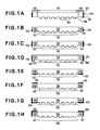
- Figure 1A shows a cross section of the mold in this embodiment.
- the mold includes a transparent member 101, a processing side 102, a light-blocking member 103, an imprint pattern portion 104, and a non-pattern portion 105.
- broken lines between the imprint pattern portion 104 and the non-pattern portion 105 in the figure are depicted for indicating a boundary therebetween for convenience of explanation.
- the mold has a first surface 106 and a second surface 107.
- the first surface 106 constitutes the processing side 102 having an imprint pattern
- the second surface 107 constitutes a side identical in location to the processing side 102 having the imprint pattern at the imprint pattern portion 104.
- the light-blocking member 103 is provided at least any one of the side 107 identical in location to the processing side 106 having the imprint pattern at the non-pattern portion 105, a side identical in location to back side at the non-pattern portion 105, and a lateral side of the mold at the non-pattern portion.
- the light-blocking member may be disposed at the lateral side of the mold.
- the mold itself can be regarded as the non-pattern portion.
- the light-blocking member used in the present invention may include not only one which completely blocks light capable of curing a photocurable resin material constituting at least a part of a work but also one which does not completely block the light. In the latter case, the light-blocking member may only be required to provide a necessary difference in degree of curing of the photocurable resin material between in an area n which the light is not blocked and in an area in which the light is blocked.
- an imprint apparatus includes a light-blocking member (light-blocking means) for blocking light with which a member to be processed is irradiated from an exposure light source not through the mold.
- a light-blocking member for blocking light with which a member to be processed is irradiated from an exposure light source not through the mold.
- the mold is constituted by providing the light-blocking member so that the photocurable resin material close to the lateral side of the mold during processing is not cured or is less cured than that located in the imprint pattern portion.
- the step-and-process method may, e.g., be the following method.
- a work is prepared by coating an entire surface of a substrate with a photocurable resin material.
- a part of the surface of the work is irradiated with light in a state in which the mold is brought into contact with the work, whereby the photocurable resin material only at the part of the surface of the substrate is cured.
- the mold is removed from the work.
- the photocurable resin material after being cured by light irradiation is no longer referred to as the photocurable resin material but is inclusively referred sometimes to as the photocurable resin material for convenience.
- the object of the present invention is to suppress or alleviate the curing of the photocurable resin material in an area in which the curing of the photocurable resin material is not intended.
- the present invention is not limited to the following embodiment.
- the area in which the curing of the photocurable resin material is not intended means, e.g., the following areas in the case where a mold has an imprint pattern portion and a non-pattern portion adjacent to the imprint pattern portion. More specifically, examples of such areas may include an area of the photocurable resin material at the non-pattern portion, an area of the photocurable resin material in the neighborhood of an outer periphery portion (lateral side) of the mold, and an area of the photocurable resin material located at an outer lateral side of the mold during contact with the photocurable resin material.
- Figure 1B shows such a constitution that the light-blocking member 103 is disposed only at a lower portion of the lateral side of the mold.
- Figure 1C shows such a constitution that the light-blocking member is protruded downwardly from the lateral side of the mold.
- a light-blocking effect is further enhanced in the case of Figure 1A , i.e., in the case where a level of the lateral side of the mold does not reach the same level as a (lower) surface of the projection constituting the imprint pattern at the imprint pattern portion 104.
- a length of the protruded portion of the light-blocking member from the lateral side of the mold may desirably be not more than a distance between the surface of the projection of the imprint pattern portion 104 and the surface 107 identical in location to the processing side of the mold at the non-pattern portion 105.
- Figure 1D shows such a constitution that a reinforcing member 108 for reinforcing the light-blocking member 103 is provided.
- the light-blocking member 103 has a thickness of approximately 50 nm. In this case, when the light-blocking member does not have a sufficient strength, it is possible to prevent breakage at the lower portion of the light-blocking member 103 by reinforcing the lower portion with the reinforcing member 108.
- Figure 1E shows that a light-blocking member 103 is disposed at a lower side (surface) 107.
- the light-blocking member 103 may desirably have a thickness of not more than the distance between the surface of the projection of the imprint pattern portion 104 and the surface 107 identical in location to the processing side of the mold.
- Figure 1F shows that a light-blocking member 103 is disposed on a back side (upper side) at the non-pattern portion 105.
- Figure 1G shows such a constitution that the light-blocking member 103 is disposed at the lower side (surface) 107 in addition to the lateral side of the mold.
- the light-blocking member 103 may desirably have a thickness of not more than the distance between the surface of the projection of the imprint pattern portion 104 and the surface 107 identical in location to the processing side of the mold.
- Figure 1H shows such a constitution that the light-blocking member 103 is disposed on the back side (upper side) at the non-pattern portion 105 in addition to the lateral side of the mold.
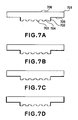
- Figures 7A to 7D are of such a projection-type wherein a third side is provided between the processing side and the back side.
- the mold includes a transparent member 701, a light-blocking member 702, a first side 703, a second side 704, a third side 705, and a back side 706.
- the light-blocking member 702 is disposed on the lateral side located between the first side 703 and the third side 705 and is disposed on the third side 705.
- the light-blocking member 702 is disposed on the third side 705.
- the light-blocking member 702 is disposed on the lateral side located between the first side 703 and the third side 705, on the third side 705, and on the lateral side located between the third side 705 and the back side 706.
- the mold includes a transparent member 701, a light-blocking member 702, imprint pattern 704 on said processing side 703, a surface 705 at the processing side on the non-pattern portion, and a back side 706.
- the light-blocking member 702 is disposed on the lateral side located between the imprint pattern 704 on said processing side 703 and surface 705 at the processing side on the non-pattern portion and is disposed on the surface 705 at the processing side on the non-pattern portion.
- a light-blocking member 702 is disposed on the surface 705 at the processing side on the non-pattern portion.
- the light-blocking member 702 is disposed on the lateral side located between the imprint pattern (704) on said processing side 703 and the surface (705) at the processing side on the non-pattern portion, on the surface (705) at the processing side on the non-pattern portion, and on the lateral side located between the surface (705) at the processing side on the non-pattern portion and the back side 706.
- the mold substrate 201 has a front side as a processing side to be subjected to processing, a back side opposite from the front side (processing side), and a lateral side connecting the front side and the back side.
- the substrate 201 is prepared.
- the substrate 201 may be formed of a light-transmissive substance including heat-resistant glass such as quartz glass or pyrex (registered trademark), and sapphire.
- a negative resist 202 is applied onto the processing side of the substrate 201 by a spin coater or the like and is irradiated with light to be modified so that it is not readily dissolved in a developing solution.
- a negative resist 202 is applied onto the back side of the substrate 201 by a spin coater or the like and is irradiated with light to be modified so that it is not readily dissolved in a developing solution.
- the coating may also be performed after a film-like mask is provided on the lateral side of the substrate so that the resist is not adhered to the lateral side of the substrate.
- a light-blocking member 203 is provided on the lateral side of the substrate.
- the light-blocking member 203 is vapor-deposited in a layer (film) of metal such as Cr on the lateral side of the substrate by sputtering, chemical vapor deposition (CVD), vacuum vapor deposition, ion plating, etc.
- the resultant metal film is only required to sufficiently block ultraviolet (UV) light and may desirably have a thickness of not more than 50 nm.
- the light-blocking member 203 may be formed of organic materials of acrylic-type, urethane-type, polycarbonate-type, etc., or of inorganic materials of carbon-type, etc. These materials may further contain other materials such as a colorant.
- step a-5 the resist 202 is removed from the substrate 201 to complete the substrate 201 with the light-blocking member 203.
- the surface of the substrate 201 is processed by a method described later to form an imprint pattern (not shown).
- step b-1 a substrate 201 is prepared.
- a light-blocking member 203 is disposed on the substrate 201 by dipping the substrate 201 in or coating the substrate 201 with a solution containing a material constituting the light-blocking member 203 or its precursor. Then, the light-blocking member 203 is fixed on the substrate 201 by removing the solvent. In the case where the light-blocking member 203 is provided only at a part of lateral side of the substrate 201, dipping of the substrate 201 may be effected in a necessary depth.
- the light-blocking member 203 may be formed of the same material as those described with reference to Figure 2A .
- step b-3 the light-blocking member 203 formed on a back side of the substrate 201 is removed by polishing the back side of the substrate 201 through chemical mechanical polishing (CMP), etc.
- CMP chemical mechanical polishing
- step b-4 a front side of the substrate 201 is polished to complete the substrate 201 provided with the light-blocking member 203 on the lateral side of the substrate 201.
- the light-blocking member 203 is not limited to those formed by the above described liquid phase deposition or vapor phase deposition but may also be formed by adhering a film-like light-blocking substance or a plate-like light-blocking substance to the substrate 201.
- steps b-2 and b-3 may also be repeated in several cycles.
- the processing side of the thus prepared substrate having the light-blocking member is subjected to formation of the imprint pattern through an ordinary patterning method such as photolithography, electron beam lithography, focused ion beam (FIB) processing, or X-ray lithography, thus completing the mold.
- an ordinary patterning method such as photolithography, electron beam lithography, focused ion beam (FIB) processing, or X-ray lithography
- the light-blocking member may also be formed after the imprint pattern is formed on the processing side of the substrate.
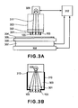
- Figure 3A shows the constitutional example of the imprint apparatus in this embodiment.
- the imprint apparatus may include a mold 301, a mold holding portion 302, a body tube 303, a photocurable resin material 304, a substrate 305, a work holding portion 306, a work pressing mechanism 307, an XY moving mechanism 308, an exposure light source 309, a light-blocking member 310, exposure light 310, and an imprint control mechanism 312.
- the imprint apparatus in this embodiment in principally constituted by the mold holding portion 302, the work holding portion 306, the work pressing mechanism 307, the XY moving mechanism 308, the exposure light source 309, and the imprint control mechanism 312.
- a work (member to be processed) constituted by the substrate 305 coated with the photocurable resin material 304 by a coating method such as spin coating or slit coating is disposed.
- the imprint apparatus further includes a position detection apparatus for effecting alignment which is not shown and omitted from explanation.
- the mold holding portion 302 effects chucking of the mold 301 by a vacuum chucking method or the like.
- the work is movable to a desired position by the XY moving mechanism 308, and the work pressing mechanism 307 can effect height adjustment (level control) and pressing of the work.
- the exposure light 311 from the exposure light source 309 passes through the body tube 303 and reaches the mold 301.
- the light 311 is restricted so as not to reach the outside of the mold 301 by limiting light fluxes with lens or diaphragm.
- the position movement, pressing, and light exposure of the work are controlled by the imprint control mechanism 312.
- the mold 301 shown in Figure 3A in this embodiment is constituted by a transparent member and is provided with a light-blocking member 103 on an entire lateral side (non-pattern portion) of the mold 301.
- a light-blocking member 103 on an entire lateral side (non-pattern portion) of the mold 301.
- an in-plane area of the work which has not been subjected to processing cannot be exposed to light, so that it is possible to prevent such a phenomenon that the photocurable resin material 304 in the in-plane area (before processing) is cured so as not to permit transfer of the imprint pattern of the mold 301.
- Figure 3B shows another example of the body tube 303 which is constituted in the following manner.
- the light-blocking member 310 is provided at necessary portions of the body tube 303 and the mold holding portion 302 so that the exposure light reaching a portion other than a necessary portion for exposure not through the mold, i.e., so-called stray light is completely blocked.
- stray light By employing such a constitution, it is possible to prepare the body tube 303 and the mold holding portion 302 with a light-transmissive material. Further, it is not necessary to limit an irradiation range of the light from the light source 309 by the lens or diaphragm.
- the exposure light emitted from the light source 309 passes through the mold to reach the back side of the mold. Even when light fluxes of the exposure light from the light source travel in a divergent manner, in parallel lines, or in a convergent manner, they are reflected or scattered by various members in some cases depending on a constitution of the imprint apparatus. Further, there is also a possibility that the exposure light leaks from a gap between the members.
- the light-blocking member 310 is provided at necessary portions of the body tube 303 and the mold holding portion 302, i.e., on the lateral side of the body tube 303 and the lateral side and the peripheral lower side of the mold holding portion 302, thus completely blocking the exposure light from reaching portions other than the necessary portions.
- the light-blocking member 310 and the light-blocking member 103 for the mold 301 in combination, an area to be exposed to light of the work is restricted to an area identical to the lower side (processing side) of the mold at the imprint pattern portion.
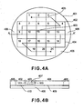
- Figures 4A and 4B are schematic views for illustrating a procedure for processing a work, wherein Figure 4A is a top view and Figure 4B is a sectional view taken along A-A' line shown in Figure 4A .
- a reference numeral 401 represents a work
- 407 represents a mold
- 408 represents a substrate
- 409 represents a photocurable resin material
- 410 represent a cured resin material after an imprint pattern is transferred onto it.
- a light-blocking member 103 is provided on an entire lateral side of the mold 407.
- a reference numeral 405 represents a processing path which is a shortest path for processing.
- numbers 1 to 21 each represents an area per one shot of processing and the processing of work is performed on the order of an increasing number.
- a reference numeral 402 indicated by a broken line shows nine areas of No. 1 to No. 9 which have been already processed.
- a reference numeral 403 indicated by a bold solid line shows a current processing area of No. 10.
- Reference numerals 404 indicated by a solid line shows even unprocessed areas of No. 11 to No. 21.
- a reference numeral 406 represents an unexposed area, in the neighborhood of an edge of the wafer (work), which is not exposed to light even after the processing of work is completed.
- the processing of work is effected by repetitively performing XY movement of the work, contact of the mold with the work, light exposure to the work, and removal of the mold.
- the work moved to the position of No. 10 is brought into contact with the mold, or the mold is brought into contact with the work.
- the photocurable resin material which cannot be accommodated between the mold and the work flows from the processing side to the outside of the processing side.
- the production process of the structure is completed. Further, in the case where the production process of the structure is used in production of a semiconductor device such as LSI, by using the resin material itself, which has been cured and formed in the imprint pattern, as an etching mask, the surface of the underlying substrate is subjected to etching so as to form a recess such as grooves corresponding to the above described imprint pattern.
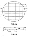
- Figures 5A and 5B show the work after the processing is completed.
- Figure 5A is a top view of the work and
- Figure 5B is a sectional view of the work taken along A-A' line shown in Figure 5A .
- a reference numeral 501 represents a work
- 502 represents an area after the processing
- 503 represents an unexposed area
- 504 represents a substrate
- 505 represents a cured resin material after a pattern is transferred onto the cured resin material
- 506 represents an uncured resin material which flows from the processing area to the outside of the processing area during the processing and is located in the neighborhood of the boundary of the processing area without being exposed to light.
- the uncured resin materials in the neighborhood of the boundary of the processing area and in the unexposed area adversely affect subsequent steps in some cases.
- the pattern portion is covered with the uncured resin material and when the etching is performed in such a state, an etching rate is changed to fail to obtain a desired pattern.
- the uncured resin materials can be blown off, or removed by washing, or cured by light exposure.
- the coating method of the photocurable resin material it is possible to use such an ink jet method that the photocurable resin material is coated on the substrate for each processing area.
- the processing is effected by using the ink jet method
- a cycle of application of resin material onto a processing area, XY movement of the work, contact of the mold with the work, light exposure to the work, and removal of the mold from the work is repeated.
- on the substrate there are three areas including an area in which the processing is effected so as to transfer the pattern onto the resin material, an area in which the processing has not been effected as yet and the substrate provided with no resin material is exposed, and an area being processed.
- the light-blocking members in this embodiment it is possible to prevent irradiation of the area, after the processing is completed, with the exposure light. As a result, the resin material in the processed area can be prevented from being excessively exposed to light.
- a reference numeral 601 represents a mold
- 602 represents exposure light
- 603 represents a substrate
- 604 represents a resin material
- 605 represents a resin material flowing from the mold 601 to the outside of the mold 601
- 606 represents a processing area in which the mold 601 has been successfully removed from the substrate 603.
- the processing area 606 includes a mold area 607 and margin area 608.
- the margin area 608 is a minimum area, located outside the mold 601, in which the resin material is cured by light exposure.
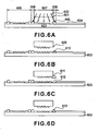
- Figure 6A shows a light exposure process.
- the exposure light is radially diverged from the light source and passes through the inside of the mold, so that the outside of the mold is irradiated with the exposure light.
- the resin material is exposed to light in not only the mold area but also the margin area.
- the pattern has a depth (thickness) of the order of approximately 100 nm but the thickness of the resin material flowing outside the mold sometimes amounts to several millimeters.
- a resin material is cured, there is a possibility that a part or all of the resin material on the substrate is removed due to the thin layer of resin material on the substrate. Further, when an amount of exposure light is small and thus the resin material is not sufficiently cured, the resin material is attached to the mold and can be dropped from the mold during movement of the mold to result in a defect.
- Figure 6B shows an example in which a small resin material piece 609 is separated from a resin material 610 and attached to the mold. Such a resin material piece 609 is sometimes dropped from the mold onto the work during the processing. When the dropped resin material piece 609 is sandwiched between the work and the mold and deposited on the processing side of the mold, from then on, the processing apparatus is a defect.
- Figure 6C shows an example in which a large resin material piece 611 is removed from the substrate 603, so that a surface 612 of the substrate 603 is exposed. In this case, the resin material piece 611 is cured and a defect is caused to occur in subsequent areas.
- Figure 6D shows an example in which a resin material portion 613 is partially raised from the substrate 603 in an area. When this area is a margin area, the resin material portion 613 is a limitative defect.
Landscapes
- Engineering & Computer Science (AREA)
- Physics & Mathematics (AREA)
- Chemical & Material Sciences (AREA)
- Nanotechnology (AREA)
- General Physics & Mathematics (AREA)
- Health & Medical Sciences (AREA)
- Crystallography & Structural Chemistry (AREA)
- Oral & Maxillofacial Surgery (AREA)
- Mathematical Physics (AREA)
- Theoretical Computer Science (AREA)
- Condensed Matter Physics & Semiconductors (AREA)
- Toxicology (AREA)
- Manufacturing & Machinery (AREA)
- Thermal Sciences (AREA)
- Mechanical Engineering (AREA)
- Shaping Of Tube Ends By Bending Or Straightening (AREA)
- Casting Or Compression Moulding Of Plastics Or The Like (AREA)
- Exposure Of Semiconductors, Excluding Electron Or Ion Beam Exposure (AREA)
- Micromachines (AREA)
- Moulds For Moulding Plastics Or The Like (AREA)
Priority Applications (1)
| Application Number | Priority Date | Filing Date | Title |
|---|---|---|---|
| EP08153570A EP1942374B1 (en) | 2005-09-06 | 2006-09-05 | Imprint method for producing structure |
Applications Claiming Priority (1)
| Application Number | Priority Date | Filing Date | Title |
|---|---|---|---|
| JP2005257431 | 2005-09-06 |
Related Child Applications (2)
| Application Number | Title | Priority Date | Filing Date |
|---|---|---|---|
| EP08153570A Division EP1942374B1 (en) | 2005-09-06 | 2006-09-05 | Imprint method for producing structure |
| EP08153570.0 Division-Into | 2008-03-28 |
Publications (2)
| Publication Number | Publication Date |
|---|---|
| EP1762893A1 EP1762893A1 (en) | 2007-03-14 |
| EP1762893B1 true EP1762893B1 (en) | 2012-11-14 |
Family
ID=37654877
Family Applications (2)
| Application Number | Title | Priority Date | Filing Date |
|---|---|---|---|
| EP06120143A Not-in-force EP1762893B1 (en) | 2005-09-06 | 2006-09-05 | Mold, imprint apparatus, and process for producing structure |
| EP08153570A Not-in-force EP1942374B1 (en) | 2005-09-06 | 2006-09-05 | Imprint method for producing structure |
Family Applications After (1)
| Application Number | Title | Priority Date | Filing Date |
|---|---|---|---|
| EP08153570A Not-in-force EP1942374B1 (en) | 2005-09-06 | 2006-09-05 | Imprint method for producing structure |
Country Status (6)
| Country | Link |
|---|---|
| US (2) | US8011916B2 (enExample) |
| EP (2) | EP1762893B1 (enExample) |
| JP (2) | JP4262271B2 (enExample) |
| KR (2) | KR100907573B1 (enExample) |
| CN (2) | CN1928712B (enExample) |
| AT (1) | ATE551631T1 (enExample) |
Cited By (1)
| Publication number | Priority date | Publication date | Assignee | Title |
|---|---|---|---|---|
| US9523919B2 (en) | 2011-05-31 | 2016-12-20 | 3M Innovative Properties Company | Methods for making differentially pattern cured microstructured articles |
Families Citing this family (90)
| Publication number | Priority date | Publication date | Assignee | Title |
|---|---|---|---|---|
| JP4262267B2 (ja) * | 2005-09-06 | 2009-05-13 | キヤノン株式会社 | モールド、インプリント装置及びデバイスの製造方法 |
| US7690910B2 (en) * | 2006-02-01 | 2010-04-06 | Canon Kabushiki Kaisha | Mold for imprint, process for producing minute structure using the mold, and process for producing the mold |
| US8850980B2 (en) * | 2006-04-03 | 2014-10-07 | Canon Nanotechnologies, Inc. | Tessellated patterns in imprint lithography |
| JP5306989B2 (ja) * | 2006-04-03 | 2013-10-02 | モレキュラー・インプリンツ・インコーポレーテッド | 複数のフィールド及びアライメント・マークを有する基板を同時にパターニングする方法 |
| JP4936519B2 (ja) * | 2006-08-18 | 2012-05-23 | 公立大学法人大阪府立大学 | ナノ構造及びマイクロ構造を有する構造体の成形用モールドの製造方法及び該モールドを用いる該構造体の製造方法 |
| JP5492369B2 (ja) * | 2006-08-21 | 2014-05-14 | 東芝機械株式会社 | 転写用の型および転写方法 |
| JP4922774B2 (ja) * | 2007-01-26 | 2012-04-25 | 株式会社東芝 | パターン形成方法及びパターン形成用モールド |
| JP5110924B2 (ja) * | 2007-03-14 | 2012-12-26 | キヤノン株式会社 | モールド、モールドの製造方法、加工装置及び加工方法 |
| KR20080105524A (ko) * | 2007-05-31 | 2008-12-04 | 삼성전자주식회사 | 마스크 몰드 및 그 제작방법과 제작된 마스크 몰드를이용한 대면적 미세패턴 성형방법 |
| JP5182470B2 (ja) * | 2007-07-17 | 2013-04-17 | 大日本印刷株式会社 | インプリントモールド |
| JP5473266B2 (ja) * | 2007-08-03 | 2014-04-16 | キヤノン株式会社 | インプリント方法および基板の加工方法、基板の加工方法による半導体デバイスの製造方法 |
| JP5274128B2 (ja) * | 2007-08-03 | 2013-08-28 | キヤノン株式会社 | インプリント方法および基板の加工方法 |
| US7854877B2 (en) * | 2007-08-14 | 2010-12-21 | Asml Netherlands B.V. | Lithography meandering order |
| KR100884811B1 (ko) * | 2007-09-07 | 2009-02-20 | 한국기계연구원 | 임프린트 리소그래피를 이용한 대면적 스탬프의 제조방법 |
| JP2009182075A (ja) * | 2008-01-30 | 2009-08-13 | Canon Inc | インプリントによる構造体の製造方法 |
| JP4799575B2 (ja) * | 2008-03-06 | 2011-10-26 | 株式会社東芝 | インプリント方法 |
| JP5258635B2 (ja) * | 2008-03-18 | 2013-08-07 | キヤノン株式会社 | ナノインプリント方法、ナノインプリントに用いられるモールド及び構造体の製造方法 |
| JP5130977B2 (ja) * | 2008-03-19 | 2013-01-30 | コニカミノルタアドバンストレイヤー株式会社 | サブマスター成形型の製造方法 |
| JP2009298041A (ja) * | 2008-06-13 | 2009-12-24 | Toshiba Corp | テンプレート及びパターン形成方法 |
| KR20110052655A (ko) * | 2008-07-25 | 2011-05-18 | 헨켈 코포레이션 | 몰드 어셈블리 및 성형 부품의 제조를 위한 감쇠된 광 방법 |
| JP2010076219A (ja) * | 2008-09-25 | 2010-04-08 | Canon Inc | ナノインプリントによる基板の加工方法 |
| JP4892025B2 (ja) * | 2008-09-26 | 2012-03-07 | 株式会社東芝 | インプリント方法 |
| KR101690643B1 (ko) | 2008-12-05 | 2016-12-28 | 리퀴디아 테크놀로지스 인코포레이티드 | 패턴 재료 제조 방법 |
| WO2010087021A1 (ja) * | 2009-02-02 | 2010-08-05 | パイオニア株式会社 | 転写装置 |
| GB2468635B (en) * | 2009-02-05 | 2014-05-14 | Api Group Plc | Production of a surface relief on a substrate |
| TWI432806B (zh) | 2009-03-26 | 2014-04-01 | 松下電器產業股份有限公司 | 具有鏡面之光波導的製造方法 |
| NL2004265A (en) | 2009-04-01 | 2010-10-04 | Asml Netherlands Bv | Imprint lithography apparatus and method. |
| JP5377053B2 (ja) * | 2009-04-17 | 2013-12-25 | 株式会社東芝 | テンプレート及びその製造方法、並びにパターン形成方法 |
| JP5407525B2 (ja) * | 2009-04-27 | 2014-02-05 | 大日本印刷株式会社 | ナノインプリント転写用基板およびナノインプリント転写方法 |
| JP5257225B2 (ja) * | 2009-04-28 | 2013-08-07 | 大日本印刷株式会社 | ナノインプリント用モールドおよびその製造方法 |
| JP5443070B2 (ja) * | 2009-06-19 | 2014-03-19 | 東京エレクトロン株式会社 | インプリントシステム |
| JP5285514B2 (ja) * | 2009-06-24 | 2013-09-11 | 東京エレクトロン株式会社 | テンプレート処理装置、インプリントシステム、離型剤処理方法、プログラム及びコンピュータ記憶媒体 |
| JP5285515B2 (ja) * | 2009-06-24 | 2013-09-11 | 東京エレクトロン株式会社 | テンプレート処理装置、インプリントシステム、離型剤処理方法、プログラム及びコンピュータ記憶媒体 |
| JP5397054B2 (ja) * | 2009-07-08 | 2014-01-22 | 大日本印刷株式会社 | ナノインプリント方法およびナノインプリント装置 |
| JP5299139B2 (ja) * | 2009-07-22 | 2013-09-25 | 大日本印刷株式会社 | ナノインプリント用モールドの製造方法 |
| US20110031650A1 (en) * | 2009-08-04 | 2011-02-10 | Molecular Imprints, Inc. | Adjacent Field Alignment |
| EP2287666B1 (de) | 2009-08-22 | 2012-06-27 | EV Group E. Thallner GmbH | Vorrichtung zum Prägen von Substraten |
| JP5532854B2 (ja) * | 2009-11-25 | 2014-06-25 | 大日本印刷株式会社 | パターン形成方法、パターン形成装置、ナノインプリントモールド及びナノインプリントモールドの製造方法 |
| JP5532939B2 (ja) * | 2010-01-14 | 2014-06-25 | 大日本印刷株式会社 | 光インプリント用のモールドおよびこれを用いた光インプリント方法 |
| JP5458975B2 (ja) * | 2010-03-10 | 2014-04-02 | 大日本印刷株式会社 | ナノインプリント用モールドの製造方法 |
| JP2012006233A (ja) * | 2010-06-24 | 2012-01-12 | Toshiba Mach Co Ltd | 型の製造方法 |
| JP5648362B2 (ja) * | 2010-08-10 | 2015-01-07 | 住友電気工業株式会社 | ナノインプリント用モールドの製造方法、ナノインプリント法による樹脂パターンの製造方法、及び、ナノインプリント用モールド |
| JP5355614B2 (ja) * | 2011-04-19 | 2013-11-27 | パナソニック株式会社 | シート状デバイスの製造装置、シート状デバイスの製造方法 |
| JP2013038117A (ja) * | 2011-08-04 | 2013-02-21 | Jx Nippon Oil & Energy Corp | 微細パターンを転写するための転写ヘッド及びそれを用いた微細パターンの形成方法 |
| JP6021365B2 (ja) * | 2012-03-12 | 2016-11-09 | キヤノン株式会社 | インプリント装置、それを用いた物品の製造方法 |
| JP5982996B2 (ja) * | 2012-04-26 | 2016-08-31 | 大日本印刷株式会社 | 異物除去方法 |
| KR20150112945A (ko) * | 2013-01-24 | 2015-10-07 | 소켄 케미칼 앤드 엔지니어링 캄파니, 리미티드 | 광투과형 임프린트용 몰드, 대면적 몰드의 제조방법 |
| JP5971561B2 (ja) * | 2013-01-29 | 2016-08-17 | 株式会社東芝 | パターン形成方法およびパターン形成装置 |
| JP5611399B2 (ja) * | 2013-03-25 | 2014-10-22 | キヤノン株式会社 | 加工装置 |
| JP6333039B2 (ja) | 2013-05-16 | 2018-05-30 | キヤノン株式会社 | インプリント装置、デバイス製造方法およびインプリント方法 |
| JP6032492B2 (ja) * | 2013-05-24 | 2016-11-30 | パナソニックIpマネジメント株式会社 | 微細パターン形成方法、及び微細パターン形成装置 |
| JP6120678B2 (ja) | 2013-05-27 | 2017-04-26 | キヤノン株式会社 | インプリント方法、インプリント装置及びデバイス製造方法 |
| JP6368075B2 (ja) * | 2013-06-26 | 2018-08-01 | キヤノン株式会社 | モールド |
| JP6315904B2 (ja) | 2013-06-28 | 2018-04-25 | キヤノン株式会社 | インプリント方法、インプリント装置及びデバイスの製造方法 |
| JP6338328B2 (ja) * | 2013-07-02 | 2018-06-06 | キヤノン株式会社 | インプリント装置、インプリント方法および物品の製造方法 |
| JP5644906B2 (ja) * | 2013-07-18 | 2014-12-24 | 大日本印刷株式会社 | ナノインプリント方法 |
| JP5821909B2 (ja) * | 2013-07-30 | 2015-11-24 | 大日本印刷株式会社 | 光インプリント用モールドおよびその製造方法 |
| US9177790B2 (en) * | 2013-10-30 | 2015-11-03 | Infineon Technologies Austria Ag | Inkjet printing in a peripheral region of a substrate |
| WO2015076147A1 (ja) * | 2013-11-22 | 2015-05-28 | 綜研化学株式会社 | ステップアンドリピート方式のインプリント技術を用いた構造体の製造方法 |
| TWI647738B (zh) * | 2013-12-10 | 2019-01-11 | 佳能奈米科技股份有限公司 | 用於零間隙壓印之壓印微影模板及方法 |
| EP3084523B1 (en) | 2013-12-19 | 2019-07-03 | Illumina, Inc. | Substrates comprising nano-patterning surfaces and methods of preparing thereof |
| JP6333035B2 (ja) * | 2014-04-15 | 2018-05-30 | キヤノン株式会社 | モールド、インプリント装置、インプリント方法、および物品の製造方法 |
| JP5773024B2 (ja) * | 2014-04-25 | 2015-09-02 | 大日本印刷株式会社 | ナノインプリントによるパターン形成装置 |
| TWI662591B (zh) * | 2014-07-08 | 2019-06-11 | 日商綜研化學股份有限公司 | 使用分步重複用壓印用模具的分步重複壓印方法、及分步重複用壓印用模具之製造方法 |
| TW201616553A (zh) | 2014-07-17 | 2016-05-01 | Soken Kagaku Kk | 分步重複式壓印裝置以及方法 |
| JP2016126240A (ja) * | 2015-01-07 | 2016-07-11 | 住友ゴム工業株式会社 | 印刷用樹脂原版の製造方法およびフレキソ印刷版 |
| JP6537277B2 (ja) * | 2015-01-23 | 2019-07-03 | キヤノン株式会社 | インプリント装置、物品製造方法 |
| JP2016159616A (ja) * | 2015-03-05 | 2016-09-05 | 富士ゼロックス株式会社 | 造形装置 |
| JP6602033B2 (ja) * | 2015-03-31 | 2019-11-06 | キヤノン株式会社 | インプリント装置、供給量分布の作成方法、インプリント方法、及び物品の製造方法 |
| JP6441181B2 (ja) * | 2015-08-04 | 2018-12-19 | 東芝メモリ株式会社 | インプリント用テンプレートおよびその製造方法、および半導体装置の製造方法 |
| KR102336560B1 (ko) | 2016-05-25 | 2021-12-08 | 다이니폰 인사츠 가부시키가이샤 | 템플릿 및 템플릿 블랭크, 그리고 임프린트용 템플릿 기판의 제조 방법, 임프린트용 템플릿의 제조 방법 및 템플릿 |
| JP6824713B2 (ja) * | 2016-11-30 | 2021-02-03 | キヤノン株式会社 | インプリント方法、インプリント装置、型、および物品の製造方法 |
| KR102288981B1 (ko) * | 2017-04-17 | 2021-08-13 | 에스케이하이닉스 주식회사 | 임프린트 템플레이트 및 임프린트 패턴 형성 방법 |
| JP7058951B2 (ja) * | 2017-05-24 | 2022-04-25 | キヤノン株式会社 | インプリント装置、および物品の製造方法 |
| CN107538945A (zh) * | 2017-08-04 | 2018-01-05 | 南京工业大学 | 一种均质光子晶体涂层的构筑工艺 |
| KR102463923B1 (ko) | 2017-09-18 | 2022-11-07 | 에스케이하이닉스 주식회사 | 임프린트 패턴 형성 방법 및 임프린트 장치 |
| US10935883B2 (en) * | 2017-09-29 | 2021-03-02 | Canon Kabushiki Kaisha | Nanoimprint template with light blocking material and method of fabrication |
| JP7027823B2 (ja) * | 2017-11-08 | 2022-03-02 | 大日本印刷株式会社 | 機能性基板及びその製造方法、並びにインプリントモールド |
| FR3075800B1 (fr) * | 2017-12-21 | 2020-10-09 | Arkema France | Couches anti adhesives pour les procedes d'impression par transfert |
| US10948818B2 (en) | 2018-03-19 | 2021-03-16 | Applied Materials, Inc. | Methods and apparatus for creating a large area imprint without a seam |
| KR102068574B1 (ko) * | 2018-05-29 | 2020-01-21 | 한국기계연구원 | 나노 임프린팅용 대면적 스탬프 제조방법 |
| WO2020050207A1 (ja) * | 2018-09-07 | 2020-03-12 | 富士フイルム株式会社 | インプリント用硬化性組成物、パターンの製造方法、半導体素子の製造方法および硬化物 |
| US11281095B2 (en) | 2018-12-05 | 2022-03-22 | Canon Kabushiki Kaisha | Frame curing template and system and method of using the frame curing template |
| JP7267589B2 (ja) * | 2019-04-23 | 2023-05-02 | Scivax株式会社 | インプリント用モールドおよび当該インプリント用モールドの製造方法並びに撮像素子製造方法 |
| JP2021044299A (ja) | 2019-09-06 | 2021-03-18 | キオクシア株式会社 | インプリント方法、半導体装置の製造方法、及びインプリント装置 |
| JP7558674B2 (ja) * | 2020-04-06 | 2024-10-01 | キヤノン株式会社 | インプリント装置、インプリント方法及び物品の製造方法 |
| JP7465146B2 (ja) * | 2020-05-12 | 2024-04-10 | キヤノン株式会社 | インプリント方法、インプリント装置、判定方法及び物品の製造方法 |
| US11747731B2 (en) | 2020-11-20 | 2023-09-05 | Canon Kabishiki Kaisha | Curing a shaped film using multiple images of a spatial light modulator |
| US12130549B2 (en) | 2021-09-27 | 2024-10-29 | Canon Kabushiki Kaisha | Method of manufacturing a template |
| US12195382B2 (en) * | 2021-12-01 | 2025-01-14 | Canon Kabushiki Kaisha | Superstrate and a method of using the same |
Family Cites Families (25)
| Publication number | Priority date | Publication date | Assignee | Title |
|---|---|---|---|---|
| JPH02289311A (ja) * | 1989-01-25 | 1990-11-29 | Hoya Corp | スタンパーおよびこのスタンパーを用いる情報記録媒体用基板の製造方法 |
| EP0614124A3 (en) | 1993-02-01 | 1994-12-14 | Nippon Kogaku Kk | Exposure device. |
| US5885514A (en) * | 1996-12-09 | 1999-03-23 | Dana Corporation | Ambient UVL-curable elastomer mold apparatus |
| US6780001B2 (en) * | 1999-07-30 | 2004-08-24 | Formfactor, Inc. | Forming tool for forming a contoured microelectronic spring mold |
| TW473823B (en) | 1999-11-18 | 2002-01-21 | Nippon Kogaku Kk | Exposure method as well as exposure apparatus, and method for manufacturing device |
| US6696220B2 (en) * | 2000-10-12 | 2004-02-24 | Board Of Regents, The University Of Texas System | Template for room temperature, low pressure micro-and nano-imprint lithography |
| US7635262B2 (en) * | 2000-07-18 | 2009-12-22 | Princeton University | Lithographic apparatus for fluid pressure imprint lithography |
| JP2002184669A (ja) | 2000-12-14 | 2002-06-28 | Hitachi Ltd | 半導体集積回路装置の製造方法 |
| US6653030B2 (en) | 2002-01-23 | 2003-11-25 | Hewlett-Packard Development Company, L.P. | Optical-mechanical feature fabrication during manufacture of semiconductors and other micro-devices and nano-devices that include micron and sub-micron features |
| JP3907504B2 (ja) | 2002-03-14 | 2007-04-18 | 三菱電機株式会社 | 半導体装置の製造方法および半導体装置製造用モールド |
| US7077992B2 (en) * | 2002-07-11 | 2006-07-18 | Molecular Imprints, Inc. | Step and repeat imprint lithography processes |
| US7070405B2 (en) | 2002-08-01 | 2006-07-04 | Molecular Imprints, Inc. | Alignment systems for imprint lithography |
| KR100488049B1 (ko) * | 2003-01-16 | 2005-05-06 | 엘지전자 주식회사 | 나노 임프린트 제조 방법 |
| TWI220267B (en) | 2003-07-31 | 2004-08-11 | Univ Nat Cheng Kung | Manufacturing method of transferring pattern with high aspect ratio |
| US7136150B2 (en) * | 2003-09-25 | 2006-11-14 | Molecular Imprints, Inc. | Imprint lithography template having opaque alignment marks |
| KR20050075580A (ko) * | 2004-01-16 | 2005-07-21 | 엘지전자 주식회사 | 나노 임프린트 리쏘그라피를 이용한 대면적 스탬프 제작방법 |
| KR100585951B1 (ko) * | 2004-02-18 | 2006-06-01 | 한국기계연구원 | 조합/분리형 독립구동이 가능한 복수 개의 모듈을 갖는 임프린팅 장치 |
| US7686970B2 (en) * | 2004-12-30 | 2010-03-30 | Asml Netherlands B.V. | Imprint lithography |
| TWI261308B (en) * | 2005-03-02 | 2006-09-01 | Ind Tech Res Inst | Micro-nanometer transfer printer |
| US20060266916A1 (en) | 2005-05-25 | 2006-11-30 | Molecular Imprints, Inc. | Imprint lithography template having a coating to reflect and/or absorb actinic energy |
| US7377764B2 (en) * | 2005-06-13 | 2008-05-27 | Asml Netherlands B.V. | Imprint lithography |
| JP4262267B2 (ja) | 2005-09-06 | 2009-05-13 | キヤノン株式会社 | モールド、インプリント装置及びデバイスの製造方法 |
| US7854877B2 (en) * | 2007-08-14 | 2010-12-21 | Asml Netherlands B.V. | Lithography meandering order |
| CN102712110B (zh) * | 2009-09-03 | 2015-07-22 | Lg电子株式会社 | 制造用于形成应用于家用电器外部的微图案膜的主模的方法,以及使用主模的膜的制造设备和方法 |
| JP5909046B2 (ja) * | 2011-03-09 | 2016-04-26 | 株式会社東芝 | 近接場露光方法 |
-
2006
- 2006-08-31 US US11/468,870 patent/US8011916B2/en active Active
- 2006-09-05 EP EP06120143A patent/EP1762893B1/en not_active Not-in-force
- 2006-09-05 AT AT08153570T patent/ATE551631T1/de active
- 2006-09-05 EP EP08153570A patent/EP1942374B1/en not_active Not-in-force
- 2006-09-05 JP JP2006240346A patent/JP4262271B2/ja not_active Expired - Fee Related
- 2006-09-06 CN CN200610128192XA patent/CN1928712B/zh not_active Expired - Fee Related
- 2006-09-06 KR KR1020060085408A patent/KR100907573B1/ko not_active Expired - Fee Related
- 2006-09-06 CN CN2009101738996A patent/CN101666974B/zh not_active Expired - Fee Related
-
2008
- 2008-02-01 JP JP2008023331A patent/JP4869263B2/ja not_active Expired - Fee Related
- 2008-06-05 KR KR1020080053161A patent/KR100886038B1/ko not_active Expired - Fee Related
-
2011
- 2011-08-01 US US13/195,410 patent/US20110284499A1/en not_active Abandoned
Cited By (1)
| Publication number | Priority date | Publication date | Assignee | Title |
|---|---|---|---|---|
| US9523919B2 (en) | 2011-05-31 | 2016-12-20 | 3M Innovative Properties Company | Methods for making differentially pattern cured microstructured articles |
Also Published As
| Publication number | Publication date |
|---|---|
| CN1928712A (zh) | 2007-03-14 |
| ATE551631T1 (de) | 2012-04-15 |
| EP1942374A1 (en) | 2008-07-09 |
| KR100907573B1 (ko) | 2009-07-14 |
| EP1942374B1 (en) | 2012-03-28 |
| JP2007103924A (ja) | 2007-04-19 |
| US8011916B2 (en) | 2011-09-06 |
| JP2008168641A (ja) | 2008-07-24 |
| CN101666974A (zh) | 2010-03-10 |
| CN101666974B (zh) | 2012-09-26 |
| EP1762893A1 (en) | 2007-03-14 |
| JP4262271B2 (ja) | 2009-05-13 |
| KR20070027467A (ko) | 2007-03-09 |
| KR100886038B1 (ko) | 2009-02-26 |
| JP4869263B2 (ja) | 2012-02-08 |
| US20070054097A1 (en) | 2007-03-08 |
| US20110284499A1 (en) | 2011-11-24 |
| CN1928712B (zh) | 2011-02-16 |
| KR20080059538A (ko) | 2008-06-30 |
Similar Documents
| Publication | Publication Date | Title |
|---|---|---|
| EP1762893B1 (en) | Mold, imprint apparatus, and process for producing structure | |
| US7935292B2 (en) | Imprinting of partial fields at the edge of the wafer | |
| US9046793B2 (en) | Light transmissive mold and apparatus for imprinting a pattern onto a material applied on a semiconductor workpiece and related methods | |
| US7510388B2 (en) | Mold, imprint method, and process for producing chip | |
| TWI426353B (zh) | 壓印微影系統及壓印方法 | |
| JP5164589B2 (ja) | インプリント装置 | |
| EP1594002A2 (en) | Method for manufacturing large area stamp for nanoimprint lithography | |
| US20090001634A1 (en) | Fine resist pattern forming method and nanoimprint mold structure | |
| US20060272535A1 (en) | Process for producing member having pattern, pattern transfer apparatus, and mold | |
| JP4290174B2 (ja) | パターンを有する部材の製造方法、パターン転写装置及びモールド | |
| JP5574802B2 (ja) | 構造体の製造方法 | |
| Aassime et al. | Conventional and un-conventional lithography for fabricating thin film functional devices | |
| JP2011014875A5 (enExample) | ||
| JP6996333B2 (ja) | ブランクス基材、インプリントモールド、インプリントモールドの製造方法及びインプリント方法 | |
| JP2024003899A (ja) | インプリントシステム、基板、インプリント方法、レプリカモールド製造方法及び、物品の製造方法 | |
| JP2023083029A (ja) | インプリント方法、パターン形成方法、インプリント装置、インプリント用モールドおよび物品の製造方法 |
Legal Events
| Date | Code | Title | Description |
|---|---|---|---|
| PUAI | Public reference made under article 153(3) epc to a published international application that has entered the european phase |
Free format text: ORIGINAL CODE: 0009012 |
|
| AK | Designated contracting states |
Kind code of ref document: A1 Designated state(s): AT BE BG CH CY CZ DE DK EE ES FI FR GB GR HU IE IS IT LI LT LU LV MC NL PL PT RO SE SI SK TR |
|
| AX | Request for extension of the european patent |
Extension state: AL BA HR MK YU |
|
| 17P | Request for examination filed |
Effective date: 20070914 |
|
| AKX | Designation fees paid |
Designated state(s): AT BE BG CH CY CZ DE DK EE ES FI FR GB GR HU IE IS IT LI LT LU LV MC NL PL PT RO SE SI SK TR |
|
| 17Q | First examination report despatched |
Effective date: 20071119 |
|
| RIC1 | Information provided on ipc code assigned before grant |
Ipc: B29C 35/08 20060101ALN20110823BHEP Ipc: B82Y 10/00 20110101ALN20110823BHEP Ipc: B29C 59/02 20060101ALN20110823BHEP Ipc: G03F 7/00 20060101AFI20110823BHEP |
|
| GRAP | Despatch of communication of intention to grant a patent |
Free format text: ORIGINAL CODE: EPIDOSNIGR1 |
|
| RIC1 | Information provided on ipc code assigned before grant |
Ipc: G03F 7/00 20060101AFI20110826BHEP Ipc: B29C 35/08 20060101ALN20110826BHEP Ipc: B29C 59/02 20060101ALN20110826BHEP Ipc: B82Y 10/00 20110101ALN20110826BHEP |
|
| RIC1 | Information provided on ipc code assigned before grant |
Ipc: B29C 35/08 20060101ALN20110930BHEP Ipc: B82Y 10/00 20110101ALN20110930BHEP Ipc: G03F 7/00 20060101AFI20110930BHEP Ipc: B29C 59/02 20060101ALN20110930BHEP |
|
| GRAS | Grant fee paid |
Free format text: ORIGINAL CODE: EPIDOSNIGR3 |
|
| GRAC | Information related to communication of intention to grant a patent modified |
Free format text: ORIGINAL CODE: EPIDOSCIGR1 |
|
| GRAA | (expected) grant |
Free format text: ORIGINAL CODE: 0009210 |
|
| AK | Designated contracting states |
Kind code of ref document: B1 Designated state(s): AT BE BG CH CY CZ DE DK EE ES FI FR GB GR HU IE IS IT LI LT LU LV MC NL PL PT RO SE SI SK TR |
|
| REG | Reference to a national code |
Ref country code: GB Ref legal event code: FG4D |
|
| REG | Reference to a national code |
Ref country code: CH Ref legal event code: EP Ref country code: AT Ref legal event code: REF Ref document number: 584284 Country of ref document: AT Kind code of ref document: T Effective date: 20121115 |
|
| REG | Reference to a national code |
Ref country code: IE Ref legal event code: FG4D |
|
| REG | Reference to a national code |
Ref country code: DE Ref legal event code: R096 Ref document number: 602006033011 Country of ref document: DE Effective date: 20130110 |
|
| REG | Reference to a national code |
Ref country code: NL Ref legal event code: T3 |
|
| REG | Reference to a national code |
Ref country code: AT Ref legal event code: MK05 Ref document number: 584284 Country of ref document: AT Kind code of ref document: T Effective date: 20121114 |
|
| REG | Reference to a national code |
Ref country code: LT Ref legal event code: MG4D |
|
| PG25 | Lapsed in a contracting state [announced via postgrant information from national office to epo] |
Ref country code: FI Free format text: LAPSE BECAUSE OF FAILURE TO SUBMIT A TRANSLATION OF THE DESCRIPTION OR TO PAY THE FEE WITHIN THE PRESCRIBED TIME-LIMIT Effective date: 20121114 Ref country code: SE Free format text: LAPSE BECAUSE OF FAILURE TO SUBMIT A TRANSLATION OF THE DESCRIPTION OR TO PAY THE FEE WITHIN THE PRESCRIBED TIME-LIMIT Effective date: 20121114 Ref country code: LT Free format text: LAPSE BECAUSE OF FAILURE TO SUBMIT A TRANSLATION OF THE DESCRIPTION OR TO PAY THE FEE WITHIN THE PRESCRIBED TIME-LIMIT Effective date: 20121114 Ref country code: ES Free format text: LAPSE BECAUSE OF FAILURE TO SUBMIT A TRANSLATION OF THE DESCRIPTION OR TO PAY THE FEE WITHIN THE PRESCRIBED TIME-LIMIT Effective date: 20130225 |
|
| PG25 | Lapsed in a contracting state [announced via postgrant information from national office to epo] |
Ref country code: SI Free format text: LAPSE BECAUSE OF FAILURE TO SUBMIT A TRANSLATION OF THE DESCRIPTION OR TO PAY THE FEE WITHIN THE PRESCRIBED TIME-LIMIT Effective date: 20121114 Ref country code: PL Free format text: LAPSE BECAUSE OF FAILURE TO SUBMIT A TRANSLATION OF THE DESCRIPTION OR TO PAY THE FEE WITHIN THE PRESCRIBED TIME-LIMIT Effective date: 20121114 Ref country code: PT Free format text: LAPSE BECAUSE OF FAILURE TO SUBMIT A TRANSLATION OF THE DESCRIPTION OR TO PAY THE FEE WITHIN THE PRESCRIBED TIME-LIMIT Effective date: 20130314 Ref country code: CY Free format text: LAPSE BECAUSE OF FAILURE TO SUBMIT A TRANSLATION OF THE DESCRIPTION OR TO PAY THE FEE WITHIN THE PRESCRIBED TIME-LIMIT Effective date: 20121114 Ref country code: BE Free format text: LAPSE BECAUSE OF FAILURE TO SUBMIT A TRANSLATION OF THE DESCRIPTION OR TO PAY THE FEE WITHIN THE PRESCRIBED TIME-LIMIT Effective date: 20121114 Ref country code: LV Free format text: LAPSE BECAUSE OF FAILURE TO SUBMIT A TRANSLATION OF THE DESCRIPTION OR TO PAY THE FEE WITHIN THE PRESCRIBED TIME-LIMIT Effective date: 20121114 Ref country code: GR Free format text: LAPSE BECAUSE OF FAILURE TO SUBMIT A TRANSLATION OF THE DESCRIPTION OR TO PAY THE FEE WITHIN THE PRESCRIBED TIME-LIMIT Effective date: 20130215 |
|
| PG25 | Lapsed in a contracting state [announced via postgrant information from national office to epo] |
Ref country code: AT Free format text: LAPSE BECAUSE OF FAILURE TO SUBMIT A TRANSLATION OF THE DESCRIPTION OR TO PAY THE FEE WITHIN THE PRESCRIBED TIME-LIMIT Effective date: 20121114 |
|
| PG25 | Lapsed in a contracting state [announced via postgrant information from national office to epo] |
Ref country code: BG Free format text: LAPSE BECAUSE OF FAILURE TO SUBMIT A TRANSLATION OF THE DESCRIPTION OR TO PAY THE FEE WITHIN THE PRESCRIBED TIME-LIMIT Effective date: 20130214 Ref country code: CZ Free format text: LAPSE BECAUSE OF FAILURE TO SUBMIT A TRANSLATION OF THE DESCRIPTION OR TO PAY THE FEE WITHIN THE PRESCRIBED TIME-LIMIT Effective date: 20121114 Ref country code: SK Free format text: LAPSE BECAUSE OF FAILURE TO SUBMIT A TRANSLATION OF THE DESCRIPTION OR TO PAY THE FEE WITHIN THE PRESCRIBED TIME-LIMIT Effective date: 20121114 Ref country code: DK Free format text: LAPSE BECAUSE OF FAILURE TO SUBMIT A TRANSLATION OF THE DESCRIPTION OR TO PAY THE FEE WITHIN THE PRESCRIBED TIME-LIMIT Effective date: 20121114 Ref country code: EE Free format text: LAPSE BECAUSE OF FAILURE TO SUBMIT A TRANSLATION OF THE DESCRIPTION OR TO PAY THE FEE WITHIN THE PRESCRIBED TIME-LIMIT Effective date: 20121114 |
|
| PG25 | Lapsed in a contracting state [announced via postgrant information from national office to epo] |
Ref country code: RO Free format text: LAPSE BECAUSE OF FAILURE TO SUBMIT A TRANSLATION OF THE DESCRIPTION OR TO PAY THE FEE WITHIN THE PRESCRIBED TIME-LIMIT Effective date: 20121114 |
|
| PLBE | No opposition filed within time limit |
Free format text: ORIGINAL CODE: 0009261 |
|
| STAA | Information on the status of an ep patent application or granted ep patent |
Free format text: STATUS: NO OPPOSITION FILED WITHIN TIME LIMIT |
|
| 26N | No opposition filed |
Effective date: 20130815 |
|
| REG | Reference to a national code |
Ref country code: DE Ref legal event code: R097 Ref document number: 602006033011 Country of ref document: DE Effective date: 20130815 |
|
| PG25 | Lapsed in a contracting state [announced via postgrant information from national office to epo] |
Ref country code: MC Free format text: LAPSE BECAUSE OF FAILURE TO SUBMIT A TRANSLATION OF THE DESCRIPTION OR TO PAY THE FEE WITHIN THE PRESCRIBED TIME-LIMIT Effective date: 20121114 |
|
| REG | Reference to a national code |
Ref country code: CH Ref legal event code: PL |
|
| GBPC | Gb: european patent ceased through non-payment of renewal fee |
Effective date: 20130905 |
|
| REG | Reference to a national code |
Ref country code: FR Ref legal event code: ST Effective date: 20140530 |
|
| REG | Reference to a national code |
Ref country code: IE Ref legal event code: MM4A |
|
| PG25 | Lapsed in a contracting state [announced via postgrant information from national office to epo] |
Ref country code: IE Free format text: LAPSE BECAUSE OF NON-PAYMENT OF DUE FEES Effective date: 20130905 Ref country code: LI Free format text: LAPSE BECAUSE OF NON-PAYMENT OF DUE FEES Effective date: 20130930 Ref country code: GB Free format text: LAPSE BECAUSE OF NON-PAYMENT OF DUE FEES Effective date: 20130905 Ref country code: CH Free format text: LAPSE BECAUSE OF NON-PAYMENT OF DUE FEES Effective date: 20130930 |
|
| PG25 | Lapsed in a contracting state [announced via postgrant information from national office to epo] |
Ref country code: FR Free format text: LAPSE BECAUSE OF NON-PAYMENT OF DUE FEES Effective date: 20130930 |
|
| PG25 | Lapsed in a contracting state [announced via postgrant information from national office to epo] |
Ref country code: TR Free format text: LAPSE BECAUSE OF FAILURE TO SUBMIT A TRANSLATION OF THE DESCRIPTION OR TO PAY THE FEE WITHIN THE PRESCRIBED TIME-LIMIT Effective date: 20121114 |
|
| PG25 | Lapsed in a contracting state [announced via postgrant information from national office to epo] |
Ref country code: LU Free format text: LAPSE BECAUSE OF NON-PAYMENT OF DUE FEES Effective date: 20130905 Ref country code: HU Free format text: LAPSE BECAUSE OF FAILURE TO SUBMIT A TRANSLATION OF THE DESCRIPTION OR TO PAY THE FEE WITHIN THE PRESCRIBED TIME-LIMIT; INVALID AB INITIO Effective date: 20060905 |
|
| PGFP | Annual fee paid to national office [announced via postgrant information from national office to epo] |
Ref country code: NL Payment date: 20150807 Year of fee payment: 10 |
|
| PGFP | Annual fee paid to national office [announced via postgrant information from national office to epo] |
Ref country code: DE Payment date: 20150930 Year of fee payment: 10 |
|
| PGFP | Annual fee paid to national office [announced via postgrant information from national office to epo] |
Ref country code: IT Payment date: 20150903 Year of fee payment: 10 |
|
| PG25 | Lapsed in a contracting state [announced via postgrant information from national office to epo] |
Ref country code: IS Free format text: LAPSE BECAUSE OF FAILURE TO SUBMIT A TRANSLATION OF THE DESCRIPTION OR TO PAY THE FEE WITHIN THE PRESCRIBED TIME-LIMIT Effective date: 20121114 |
|
| REG | Reference to a national code |
Ref country code: DE Ref legal event code: R119 Ref document number: 602006033011 Country of ref document: DE |
|
| REG | Reference to a national code |
Ref country code: NL Ref legal event code: MM Effective date: 20161001 |
|
| PG25 | Lapsed in a contracting state [announced via postgrant information from national office to epo] |
Ref country code: NL Free format text: LAPSE BECAUSE OF NON-PAYMENT OF DUE FEES Effective date: 20161001 |
|
| PG25 | Lapsed in a contracting state [announced via postgrant information from national office to epo] |
Ref country code: DE Free format text: LAPSE BECAUSE OF NON-PAYMENT OF DUE FEES Effective date: 20170401 |
|
| PG25 | Lapsed in a contracting state [announced via postgrant information from national office to epo] |
Ref country code: IT Free format text: LAPSE BECAUSE OF NON-PAYMENT OF DUE FEES Effective date: 20160905 |