EP1687830B1 - Organische halbleiterschicht-formulierungen mit polyacenen und organischen binderpolymeren - Google Patents
Organische halbleiterschicht-formulierungen mit polyacenen und organischen binderpolymeren Download PDFInfo
- Publication number
- EP1687830B1 EP1687830B1 EP04819715A EP04819715A EP1687830B1 EP 1687830 B1 EP1687830 B1 EP 1687830B1 EP 04819715 A EP04819715 A EP 04819715A EP 04819715 A EP04819715 A EP 04819715A EP 1687830 B1 EP1687830 B1 EP 1687830B1
- Authority
- EP
- European Patent Office
- Prior art keywords
- group
- semiconducting layer
- organic semiconducting
- organic
- binder
- Prior art date
- Legal status (The legal status is an assumption and is not a legal conclusion. Google has not performed a legal analysis and makes no representation as to the accuracy of the status listed.)
- Active
Links
- 239000000203 mixture Substances 0.000 title claims abstract description 111
- 238000009472 formulation Methods 0.000 title claims abstract description 82
- 239000011230 binding agent Substances 0.000 title claims description 167
- 229920003026 Acene Polymers 0.000 title claims description 78
- 229920000642 polymer Polymers 0.000 title claims description 21
- 150000001875 compounds Chemical class 0.000 claims abstract description 112
- 230000005669 field effect Effects 0.000 claims abstract description 21
- -1 sulpho, sulphonyl Chemical group 0.000 claims description 139
- YMWUJEATGCHHMB-UHFFFAOYSA-N Dichloromethane Chemical compound ClCCl YMWUJEATGCHHMB-UHFFFAOYSA-N 0.000 claims description 81
- 239000002904 solvent Substances 0.000 claims description 69
- WYURNTSHIVDZCO-UHFFFAOYSA-N Tetrahydrofuran Chemical compound C1CCOC1 WYURNTSHIVDZCO-UHFFFAOYSA-N 0.000 claims description 65
- 239000004065 semiconductor Substances 0.000 claims description 41
- CSCPPACGZOOCGX-UHFFFAOYSA-N Acetone Chemical compound CC(C)=O CSCPPACGZOOCGX-UHFFFAOYSA-N 0.000 claims description 38
- 239000007787 solid Substances 0.000 claims description 36
- YLQBMQCUIZJEEH-UHFFFAOYSA-N tetrahydrofuran Natural products C=1C=COC=1 YLQBMQCUIZJEEH-UHFFFAOYSA-N 0.000 claims description 32
- 229920006395 saturated elastomer Polymers 0.000 claims description 30
- 125000001424 substituent group Chemical group 0.000 claims description 29
- 125000003118 aryl group Chemical group 0.000 claims description 28
- 125000001183 hydrocarbyl group Chemical group 0.000 claims description 28
- 238000000034 method Methods 0.000 claims description 26
- YXFVVABEGXRONW-UHFFFAOYSA-N Toluene Chemical compound CC1=CC=CC=C1 YXFVVABEGXRONW-UHFFFAOYSA-N 0.000 claims description 25
- IAZDPXIOMUYVGZ-UHFFFAOYSA-N Dimethylsulphoxide Chemical compound CS(C)=O IAZDPXIOMUYVGZ-UHFFFAOYSA-N 0.000 claims description 24
- 125000005843 halogen group Chemical group 0.000 claims description 23
- 239000000758 substrate Substances 0.000 claims description 23
- RFFLAFLAYFXFSW-UHFFFAOYSA-N 1,2-dichlorobenzene Chemical compound ClC1=CC=CC=C1Cl RFFLAFLAYFXFSW-UHFFFAOYSA-N 0.000 claims description 22
- AIXAANGOTKPUOY-UHFFFAOYSA-N carbachol Chemical group [Cl-].C[N+](C)(C)CCOC(N)=O AIXAANGOTKPUOY-UHFFFAOYSA-N 0.000 claims description 19
- 239000007788 liquid Substances 0.000 claims description 19
- 125000000217 alkyl group Chemical group 0.000 claims description 18
- 125000004432 carbon atom Chemical group C* 0.000 claims description 17
- 229920001577 copolymer Polymers 0.000 claims description 17
- PPBRXRYQALVLMV-UHFFFAOYSA-N Styrene Chemical compound C=CC1=CC=CC=C1 PPBRXRYQALVLMV-UHFFFAOYSA-N 0.000 claims description 16
- 239000011347 resin Substances 0.000 claims description 15
- 229920005989 resin Polymers 0.000 claims description 15
- URLKBWYHVLBVBO-UHFFFAOYSA-N Para-Xylene Chemical group CC1=CC=C(C)C=C1 URLKBWYHVLBVBO-UHFFFAOYSA-N 0.000 claims description 14
- 229910052739 hydrogen Inorganic materials 0.000 claims description 13
- 239000001257 hydrogen Substances 0.000 claims description 12
- 125000002496 methyl group Chemical group [H]C([H])([H])* 0.000 claims description 12
- 238000002156 mixing Methods 0.000 claims description 12
- 125000003808 silyl group Chemical group [H][Si]([H])([H])[*] 0.000 claims description 12
- 229910052760 oxygen Inorganic materials 0.000 claims description 11
- 125000001997 phenyl group Chemical group [H]C1=C([H])C([H])=C(*)C([H])=C1[H] 0.000 claims description 11
- 230000008569 process Effects 0.000 claims description 11
- KAKZBPTYRLMSJV-UHFFFAOYSA-N Butadiene Chemical compound C=CC=C KAKZBPTYRLMSJV-UHFFFAOYSA-N 0.000 claims description 10
- XUIMIQQOPSSXEZ-UHFFFAOYSA-N Silicon Chemical group [Si] XUIMIQQOPSSXEZ-UHFFFAOYSA-N 0.000 claims description 10
- RDOXTESZEPMUJZ-UHFFFAOYSA-N anisole Chemical compound COC1=CC=CC=C1 RDOXTESZEPMUJZ-UHFFFAOYSA-N 0.000 claims description 10
- 239000002243 precursor Substances 0.000 claims description 10
- 229910052710 silicon Inorganic materials 0.000 claims description 10
- 239000010703 silicon Substances 0.000 claims description 10
- 125000000008 (C1-C10) alkyl group Chemical group 0.000 claims description 9
- 125000004178 (C1-C4) alkyl group Chemical group 0.000 claims description 9
- HSFWRNGVRCDJHI-UHFFFAOYSA-N alpha-acetylene Natural products C#C HSFWRNGVRCDJHI-UHFFFAOYSA-N 0.000 claims description 9
- 125000004093 cyano group Chemical group *C#N 0.000 claims description 9
- 125000004435 hydrogen atom Chemical group [H]* 0.000 claims description 9
- 239000000178 monomer Substances 0.000 claims description 9
- 238000007639 printing Methods 0.000 claims description 9
- CXWXQJXEFPUFDZ-UHFFFAOYSA-N tetralin Chemical compound C1=CC=C2CCCCC2=C1 CXWXQJXEFPUFDZ-UHFFFAOYSA-N 0.000 claims description 9
- UFHFLCQGNIYNRP-UHFFFAOYSA-N Hydrogen Chemical compound [H][H] UFHFLCQGNIYNRP-UHFFFAOYSA-N 0.000 claims description 8
- 239000004793 Polystyrene Substances 0.000 claims description 8
- NINIDFKCEFEMDL-UHFFFAOYSA-N Sulfur Chemical group [S] NINIDFKCEFEMDL-UHFFFAOYSA-N 0.000 claims description 8
- 238000000151 deposition Methods 0.000 claims description 8
- 229910052731 fluorine Inorganic materials 0.000 claims description 8
- 125000000547 substituted alkyl group Chemical group 0.000 claims description 8
- 125000000304 alkynyl group Chemical group 0.000 claims description 7
- 125000003710 aryl alkyl group Chemical group 0.000 claims description 7
- 238000004519 manufacturing process Methods 0.000 claims description 7
- ZWEHNKRNPOVVGH-UHFFFAOYSA-N 2-Butanone Chemical compound CCC(C)=O ZWEHNKRNPOVVGH-UHFFFAOYSA-N 0.000 claims description 6
- XEKOWRVHYACXOJ-UHFFFAOYSA-N Ethyl acetate Chemical compound CCOC(C)=O XEKOWRVHYACXOJ-UHFFFAOYSA-N 0.000 claims description 6
- ZMXDDKWLCZADIW-UHFFFAOYSA-N N,N-Dimethylformamide Chemical compound CN(C)C=O ZMXDDKWLCZADIW-UHFFFAOYSA-N 0.000 claims description 6
- QVGXLLKOCUKJST-UHFFFAOYSA-N atomic oxygen Chemical compound [O] QVGXLLKOCUKJST-UHFFFAOYSA-N 0.000 claims description 6
- 229910052801 chlorine Inorganic materials 0.000 claims description 6
- 125000002534 ethynyl group Chemical group [H]C#C* 0.000 claims description 6
- 238000001704 evaporation Methods 0.000 claims description 6
- 125000000449 nitro group Chemical group [O-][N+](*)=O 0.000 claims description 6
- 239000001301 oxygen Substances 0.000 claims description 6
- 229920002223 polystyrene Polymers 0.000 claims description 6
- 238000005507 spraying Methods 0.000 claims description 6
- 239000005977 Ethylene Substances 0.000 claims description 5
- CTQNGGLPUBDAKN-UHFFFAOYSA-N O-Xylene Chemical group CC1=CC=CC=C1C CTQNGGLPUBDAKN-UHFFFAOYSA-N 0.000 claims description 5
- 125000003342 alkenyl group Chemical group 0.000 claims description 5
- 229910052794 bromium Inorganic materials 0.000 claims description 5
- 229910052799 carbon Inorganic materials 0.000 claims description 5
- 125000002485 formyl group Chemical group [H]C(*)=O 0.000 claims description 5
- 150000002430 hydrocarbons Chemical group 0.000 claims description 5
- 125000002887 hydroxy group Chemical group [H]O* 0.000 claims description 5
- 238000007641 inkjet printing Methods 0.000 claims description 5
- QPFMBZIOSGYJDE-UHFFFAOYSA-N 1,1,2,2-tetrachloroethane Chemical compound ClC(Cl)C(Cl)Cl QPFMBZIOSGYJDE-UHFFFAOYSA-N 0.000 claims description 4
- KVNYFPKFSJIPBJ-UHFFFAOYSA-N 1,2-diethylbenzene Chemical compound CCC1=CC=CC=C1CC KVNYFPKFSJIPBJ-UHFFFAOYSA-N 0.000 claims description 4
- 125000003903 2-propenyl group Chemical group [H]C([*])([H])C([H])=C([H])[H] 0.000 claims description 4
- HEDRZPFGACZZDS-UHFFFAOYSA-N Chloroform Chemical compound ClC(Cl)Cl HEDRZPFGACZZDS-UHFFFAOYSA-N 0.000 claims description 4
- VGGSQFUCUMXWEO-UHFFFAOYSA-N Ethene Chemical compound C=C VGGSQFUCUMXWEO-UHFFFAOYSA-N 0.000 claims description 4
- YNAVUWVOSKDBBP-UHFFFAOYSA-N Morpholine Chemical compound C1COCCN1 YNAVUWVOSKDBBP-UHFFFAOYSA-N 0.000 claims description 4
- MOYAFQVGZZPNRA-UHFFFAOYSA-N Terpinolene Chemical compound CC(C)=C1CCC(C)=CC1 MOYAFQVGZZPNRA-UHFFFAOYSA-N 0.000 claims description 4
- 125000004429 atom Chemical group 0.000 claims description 4
- DKPFZGUDAPQIHT-UHFFFAOYSA-N butyl acetate Chemical compound CCCCOC(C)=O DKPFZGUDAPQIHT-UHFFFAOYSA-N 0.000 claims description 4
- 239000003990 capacitor Substances 0.000 claims description 4
- NNBZCPXTIHJBJL-UHFFFAOYSA-N decalin Chemical compound C1CCCC2CCCCC21 NNBZCPXTIHJBJL-UHFFFAOYSA-N 0.000 claims description 4
- 238000007598 dipping method Methods 0.000 claims description 4
- 230000008020 evaporation Effects 0.000 claims description 4
- 229910052732 germanium Chemical group 0.000 claims description 4
- GNPVGFCGXDBREM-UHFFFAOYSA-N germanium atom Chemical group [Ge] GNPVGFCGXDBREM-UHFFFAOYSA-N 0.000 claims description 4
- 238000011065 in-situ storage Methods 0.000 claims description 4
- XMGQYMWWDOXHJM-UHFFFAOYSA-N limonene Chemical compound CC(=C)C1CCC(C)=CC1 XMGQYMWWDOXHJM-UHFFFAOYSA-N 0.000 claims description 4
- IVSZLXZYQVIEFR-UHFFFAOYSA-N m-xylene Chemical group CC1=CC=CC(C)=C1 IVSZLXZYQVIEFR-UHFFFAOYSA-N 0.000 claims description 4
- UZKWTJUDCOPSNM-UHFFFAOYSA-N methoxybenzene Substances CCCCOC=C UZKWTJUDCOPSNM-UHFFFAOYSA-N 0.000 claims description 4
- 238000010422 painting Methods 0.000 claims description 4
- 229920000314 poly p-methyl styrene Polymers 0.000 claims description 4
- 239000011877 solvent mixture Substances 0.000 claims description 4
- 125000000229 (C1-C4)alkoxy group Chemical group 0.000 claims description 3
- 125000000041 C6-C10 aryl group Chemical group 0.000 claims description 3
- 239000005062 Polybutadiene Substances 0.000 claims description 3
- XYLMUPLGERFSHI-UHFFFAOYSA-N alpha-Methylstyrene Chemical compound CC(=C)C1=CC=CC=C1 XYLMUPLGERFSHI-UHFFFAOYSA-N 0.000 claims description 3
- 150000001555 benzenes Chemical class 0.000 claims description 3
- 238000009835 boiling Methods 0.000 claims description 3
- ZHNUHDYFZUAESO-UHFFFAOYSA-N formamide Substances NC=O ZHNUHDYFZUAESO-UHFFFAOYSA-N 0.000 claims description 3
- 125000000623 heterocyclic group Chemical group 0.000 claims description 3
- 239000003960 organic solvent Substances 0.000 claims description 3
- 229920003227 poly(N-vinyl carbazole) Polymers 0.000 claims description 3
- 229920002857 polybutadiene Polymers 0.000 claims description 3
- 125000003837 (C1-C20) alkyl group Chemical group 0.000 claims description 2
- 125000006649 (C2-C20) alkynyl group Chemical group 0.000 claims description 2
- UOCLXMDMGBRAIB-UHFFFAOYSA-N 1,1,1-trichloroethane Chemical compound CC(Cl)(Cl)Cl UOCLXMDMGBRAIB-UHFFFAOYSA-N 0.000 claims description 2
- WSLDOOZREJYCGB-UHFFFAOYSA-N 1,2-Dichloroethane Chemical compound ClCCCl WSLDOOZREJYCGB-UHFFFAOYSA-N 0.000 claims description 2
- RYHBNJHYFVUHQT-UHFFFAOYSA-N 1,4-Dioxane Chemical compound C1COCCO1 RYHBNJHYFVUHQT-UHFFFAOYSA-N 0.000 claims description 2
- OEVVKKAVYQFQNV-UHFFFAOYSA-N 1-ethenyl-2,4-dimethylbenzene Chemical compound CC1=CC=C(C=C)C(C)=C1 OEVVKKAVYQFQNV-UHFFFAOYSA-N 0.000 claims description 2
- QCWXDVFBZVHKLV-UHFFFAOYSA-N 1-tert-butyl-4-methylbenzene Chemical compound CC1=CC=C(C(C)(C)C)C=C1 QCWXDVFBZVHKLV-UHFFFAOYSA-N 0.000 claims description 2
- BXVVMSMTWXVEOH-UHFFFAOYSA-N 3,6-bis(difluoromethylidene)cyclohexa-1,4-diene Chemical group FC(F)=C1C=CC(=C(F)F)C=C1 BXVVMSMTWXVEOH-UHFFFAOYSA-N 0.000 claims description 2
- 125000006374 C2-C10 alkenyl group Chemical group 0.000 claims description 2
- 125000005865 C2-C10alkynyl group Chemical group 0.000 claims description 2
- 125000003358 C2-C20 alkenyl group Chemical group 0.000 claims description 2
- BVKZGUZCCUSVTD-UHFFFAOYSA-L Carbonate Chemical compound [O-]C([O-])=O BVKZGUZCCUSVTD-UHFFFAOYSA-L 0.000 claims description 2
- 206010073306 Exposure to radiation Diseases 0.000 claims description 2
- FXHOOIRPVKKKFG-UHFFFAOYSA-N N,N-Dimethylacetamide Chemical compound CN(C)C(C)=O FXHOOIRPVKKKFG-UHFFFAOYSA-N 0.000 claims description 2
- 239000004698 Polyethylene Substances 0.000 claims description 2
- 229920002367 Polyisobutene Polymers 0.000 claims description 2
- 239000004743 Polypropylene Substances 0.000 claims description 2
- 125000002877 alkyl aryl group Chemical group 0.000 claims description 2
- WUOACPNHFRMFPN-UHFFFAOYSA-N alpha-terpineol Chemical compound CC1=CCC(C(C)(C)O)CC1 WUOACPNHFRMFPN-UHFFFAOYSA-N 0.000 claims description 2
- MVPPADPHJFYWMZ-UHFFFAOYSA-N chlorobenzene Chemical compound ClC1=CC=CC=C1 MVPPADPHJFYWMZ-UHFFFAOYSA-N 0.000 claims description 2
- UUAGAQFQZIEFAH-UHFFFAOYSA-N chlorotrifluoroethylene Chemical group FC(F)=C(F)Cl UUAGAQFQZIEFAH-UHFFFAOYSA-N 0.000 claims description 2
- 125000000392 cycloalkenyl group Chemical group 0.000 claims description 2
- 125000000753 cycloalkyl group Chemical group 0.000 claims description 2
- 229930007927 cymene Natural products 0.000 claims description 2
- SQIFACVGCPWBQZ-UHFFFAOYSA-N delta-terpineol Natural products CC(C)(O)C1CCC(=C)CC1 SQIFACVGCPWBQZ-UHFFFAOYSA-N 0.000 claims description 2
- KWKXNDCHNDYVRT-UHFFFAOYSA-N dodecylbenzene Chemical compound CCCCCCCCCCCCC1=CC=CC=C1 KWKXNDCHNDYVRT-UHFFFAOYSA-N 0.000 claims description 2
- 238000010894 electron beam technology Methods 0.000 claims description 2
- 235000013847 iso-butane Nutrition 0.000 claims description 2
- 229940087305 limonene Drugs 0.000 claims description 2
- 235000001510 limonene Nutrition 0.000 claims description 2
- 229940078552 o-xylene Drugs 0.000 claims description 2
- HFPZCAJZSCWRBC-UHFFFAOYSA-N p-cymene Chemical compound CC(C)C1=CC=C(C)C=C1 HFPZCAJZSCWRBC-UHFFFAOYSA-N 0.000 claims description 2
- 150000008379 phenol ethers Chemical class 0.000 claims description 2
- 229920001596 poly (chlorostyrenes) Polymers 0.000 claims description 2
- 229920000052 poly(p-xylylene) Polymers 0.000 claims description 2
- 229920002776 polycyclohexyl methacrylate Polymers 0.000 claims description 2
- 229920000573 polyethylene Polymers 0.000 claims description 2
- 229920001195 polyisoprene Polymers 0.000 claims description 2
- 229920000307 polymer substrate Polymers 0.000 claims description 2
- 229920000306 polymethylpentene Polymers 0.000 claims description 2
- 239000011116 polymethylpentene Substances 0.000 claims description 2
- 229920001155 polypropylene Polymers 0.000 claims description 2
- 150000003216 pyrazines Chemical class 0.000 claims description 2
- 150000003222 pyridines Chemical class 0.000 claims description 2
- 150000003230 pyrimidines Chemical class 0.000 claims description 2
- 150000004040 pyrrolidinones Chemical class 0.000 claims description 2
- 239000000126 substance Substances 0.000 claims description 2
- 229940116411 terpineol Drugs 0.000 claims description 2
- NNPPMTNAJDCUHE-UHFFFAOYSA-N trimethylmethane Natural products CC(C)C NNPPMTNAJDCUHE-UHFFFAOYSA-N 0.000 claims description 2
- PXXNTAGJWPJAGM-UHFFFAOYSA-N vertaline Natural products C1C2C=3C=C(OC)C(OC)=CC=3OC(C=C3)=CC=C3CCC(=O)OC1CC1N2CCCC1 PXXNTAGJWPJAGM-UHFFFAOYSA-N 0.000 claims description 2
- 150000003738 xylenes Chemical class 0.000 claims description 2
- 239000000243 solution Substances 0.000 description 105
- 239000010410 layer Substances 0.000 description 86
- VLKZOEOYAKHREP-UHFFFAOYSA-N n-Hexane Chemical compound CCCCCC VLKZOEOYAKHREP-UHFFFAOYSA-N 0.000 description 65
- 230000037230 mobility Effects 0.000 description 55
- HEDRZPFGACZZDS-MICDWDOJSA-N Trichloro(2H)methane Chemical compound [2H]C(Cl)(Cl)Cl HEDRZPFGACZZDS-MICDWDOJSA-N 0.000 description 46
- 239000011541 reaction mixture Substances 0.000 description 38
- VYPSYNLAJGMNEJ-UHFFFAOYSA-N Silicium dioxide Chemical compound O=[Si]=O VYPSYNLAJGMNEJ-UHFFFAOYSA-N 0.000 description 28
- 230000015572 biosynthetic process Effects 0.000 description 27
- 238000003786 synthesis reaction Methods 0.000 description 26
- 229940125904 compound 1 Drugs 0.000 description 23
- 239000000463 material Substances 0.000 description 21
- SLIUAWYAILUBJU-UHFFFAOYSA-N pentacene Chemical compound C1=CC=CC2=CC3=CC4=CC5=CC=CC=C5C=C4C=C3C=C21 SLIUAWYAILUBJU-UHFFFAOYSA-N 0.000 description 20
- HEMHJVSKTPXQMS-UHFFFAOYSA-M Sodium hydroxide Chemical compound [OH-].[Na+] HEMHJVSKTPXQMS-UHFFFAOYSA-M 0.000 description 18
- 238000005160 1H NMR spectroscopy Methods 0.000 description 17
- CDBYLPFSWZWCQE-UHFFFAOYSA-L Sodium Carbonate Chemical compound [Na+].[Na+].[O-]C([O-])=O CDBYLPFSWZWCQE-UHFFFAOYSA-L 0.000 description 17
- 150000002964 pentacenes Chemical class 0.000 description 17
- LFQSCWFLJHTTHZ-UHFFFAOYSA-N Ethanol Chemical compound CCO LFQSCWFLJHTTHZ-UHFFFAOYSA-N 0.000 description 16
- MZRVEZGGRBJDDB-UHFFFAOYSA-N N-Butyllithium Chemical compound [Li]CCCC MZRVEZGGRBJDDB-UHFFFAOYSA-N 0.000 description 16
- 238000000746 purification Methods 0.000 description 15
- XLYOFNOQVPJJNP-UHFFFAOYSA-N water Substances O XLYOFNOQVPJJNP-UHFFFAOYSA-N 0.000 description 15
- CSNNHWWHGAXBCP-UHFFFAOYSA-L Magnesium sulfate Chemical compound [Mg+2].[O-][S+2]([O-])([O-])[O-] CSNNHWWHGAXBCP-UHFFFAOYSA-L 0.000 description 14
- 238000000576 coating method Methods 0.000 description 13
- 239000010408 film Substances 0.000 description 13
- RTZKZFJDLAIYFH-UHFFFAOYSA-N Diethyl ether Chemical compound CCOCC RTZKZFJDLAIYFH-UHFFFAOYSA-N 0.000 description 12
- 229910021626 Tin(II) chloride Inorganic materials 0.000 description 12
- 239000011248 coating agent Substances 0.000 description 12
- 238000001816 cooling Methods 0.000 description 12
- AXZWODMDQAVCJE-UHFFFAOYSA-L tin(II) chloride (anhydrous) Chemical compound [Cl-].[Cl-].[Sn+2] AXZWODMDQAVCJE-UHFFFAOYSA-L 0.000 description 12
- 238000004128 high performance liquid chromatography Methods 0.000 description 11
- ZMANZCXQSJIPKH-UHFFFAOYSA-N Triethylamine Chemical compound CCN(CC)CC ZMANZCXQSJIPKH-UHFFFAOYSA-N 0.000 description 9
- 230000000052 comparative effect Effects 0.000 description 9
- 229920003251 poly(α-methylstyrene) Polymers 0.000 description 9
- 125000003545 alkoxy group Chemical group 0.000 description 8
- 239000003480 eluent Substances 0.000 description 8
- 125000001449 isopropyl group Chemical group [H]C([H])([H])C([H])(*)C([H])([H])[H] 0.000 description 8
- 229910000029 sodium carbonate Inorganic materials 0.000 description 8
- HCHKCACWOHOZIP-UHFFFAOYSA-N Zinc Chemical compound [Zn] HCHKCACWOHOZIP-UHFFFAOYSA-N 0.000 description 7
- 239000008186 active pharmaceutical agent Substances 0.000 description 7
- 238000004440 column chromatography Methods 0.000 description 7
- 125000001495 ethyl group Chemical group [H]C([H])([H])C([H])([H])* 0.000 description 7
- KZGWPHUWNWRTEP-UHFFFAOYSA-N ethynyl-tri(propan-2-yl)silane Chemical group CC(C)[Si](C#C)(C(C)C)C(C)C KZGWPHUWNWRTEP-UHFFFAOYSA-N 0.000 description 7
- 229910052943 magnesium sulfate Inorganic materials 0.000 description 7
- 238000005259 measurement Methods 0.000 description 7
- 239000000741 silica gel Substances 0.000 description 7
- 229910002027 silica gel Inorganic materials 0.000 description 7
- 125000003107 substituted aryl group Chemical group 0.000 description 7
- AZQWKYJCGOJGHM-UHFFFAOYSA-N 1,4-benzoquinone Chemical compound O=C1C=CC(=O)C=C1 AZQWKYJCGOJGHM-UHFFFAOYSA-N 0.000 description 6
- 238000004293 19F NMR spectroscopy Methods 0.000 description 6
- 229920001400 block copolymer Polymers 0.000 description 6
- 239000012212 insulator Substances 0.000 description 6
- 235000019341 magnesium sulphate Nutrition 0.000 description 6
- IUYHWZFSGMZEOG-UHFFFAOYSA-M magnesium;propane;chloride Chemical compound [Mg+2].[Cl-].C[CH-]C IUYHWZFSGMZEOG-UHFFFAOYSA-M 0.000 description 6
- 125000001181 organosilyl group Chemical group [SiH3]* 0.000 description 6
- CTSLXHKWHWQRSH-UHFFFAOYSA-N oxalyl chloride Chemical compound ClC(=O)C(Cl)=O CTSLXHKWHWQRSH-UHFFFAOYSA-N 0.000 description 6
- UFCVADNIXDUEFZ-UHFFFAOYSA-N pentacene-6,13-dione Chemical compound C1=CC=C2C=C3C(=O)C4=CC5=CC=CC=C5C=C4C(=O)C3=CC2=C1 UFCVADNIXDUEFZ-UHFFFAOYSA-N 0.000 description 6
- 239000000843 powder Substances 0.000 description 6
- 230000009467 reduction Effects 0.000 description 6
- 229910052717 sulfur Inorganic materials 0.000 description 6
- 238000001644 13C nuclear magnetic resonance spectroscopy Methods 0.000 description 5
- YTPLMLYBLZKORZ-UHFFFAOYSA-N Thiophene Chemical compound C=1C=CSC=1 YTPLMLYBLZKORZ-UHFFFAOYSA-N 0.000 description 5
- 150000004982 aromatic amines Chemical group 0.000 description 5
- 125000004104 aryloxy group Chemical group 0.000 description 5
- 239000012045 crude solution Substances 0.000 description 5
- 229910052757 nitrogen Inorganic materials 0.000 description 5
- 125000001436 propyl group Chemical group [H]C([*])([H])C([H])([H])C([H])([H])[H] 0.000 description 5
- 239000000377 silicon dioxide Substances 0.000 description 5
- 238000003756 stirring Methods 0.000 description 5
- IJGRMHOSHXDMSA-UHFFFAOYSA-N Atomic nitrogen Chemical compound N#N IJGRMHOSHXDMSA-UHFFFAOYSA-N 0.000 description 4
- DTQVDTLACAAQTR-UHFFFAOYSA-N Trifluoroacetic acid Chemical compound OC(=O)C(F)(F)F DTQVDTLACAAQTR-UHFFFAOYSA-N 0.000 description 4
- 239000007864 aqueous solution Substances 0.000 description 4
- 238000006243 chemical reaction Methods 0.000 description 4
- 238000004587 chromatography analysis Methods 0.000 description 4
- DCZFGQYXRKMVFG-UHFFFAOYSA-N cyclohexane-1,4-dione Chemical compound O=C1CCC(=O)CC1 DCZFGQYXRKMVFG-UHFFFAOYSA-N 0.000 description 4
- ZUOUZKKEUPVFJK-UHFFFAOYSA-N diphenyl Chemical compound C1=CC=CC=C1C1=CC=CC=C1 ZUOUZKKEUPVFJK-UHFFFAOYSA-N 0.000 description 4
- 238000005516 engineering process Methods 0.000 description 4
- IIEWJVIFRVWJOD-UHFFFAOYSA-N ethylcyclohexane Chemical compound CCC1CCCCC1 IIEWJVIFRVWJOD-UHFFFAOYSA-N 0.000 description 4
- 239000002244 precipitate Substances 0.000 description 4
- 238000010992 reflux Methods 0.000 description 4
- 238000004528 spin coating Methods 0.000 description 4
- 125000000025 triisopropylsilyl group Chemical group C(C)(C)[Si](C(C)C)(C(C)C)* 0.000 description 4
- 239000004215 Carbon black (E152) Substances 0.000 description 3
- OKKJLVBELUTLKV-UHFFFAOYSA-N Methanol Chemical compound OC OKKJLVBELUTLKV-UHFFFAOYSA-N 0.000 description 3
- 239000004372 Polyvinyl alcohol Substances 0.000 description 3
- ZUGKYQRAGXKKTO-UHFFFAOYSA-N [4,5-difluoro-2-(hydroxymethyl)phenyl]methanol Chemical compound OCC1=CC(F)=C(F)C=C1CO ZUGKYQRAGXKKTO-UHFFFAOYSA-N 0.000 description 3
- 238000009825 accumulation Methods 0.000 description 3
- 125000002015 acyclic group Chemical group 0.000 description 3
- 125000003277 amino group Chemical group 0.000 description 3
- 125000002102 aryl alkyloxo group Chemical group 0.000 description 3
- 239000002800 charge carrier Substances 0.000 description 3
- 238000010790 dilution Methods 0.000 description 3
- 239000012895 dilution Substances 0.000 description 3
- 238000001035 drying Methods 0.000 description 3
- RMBPEFMHABBEKP-UHFFFAOYSA-N fluorene Chemical compound C1=CC=C2C3=C[CH]C=CC3=CC2=C1 RMBPEFMHABBEKP-UHFFFAOYSA-N 0.000 description 3
- 125000005842 heteroatom Chemical group 0.000 description 3
- 229930195733 hydrocarbon Natural products 0.000 description 3
- NIHNNTQXNPWCJQ-UHFFFAOYSA-N o-biphenylenemethane Natural products C1=CC=C2CC3=CC=CC=C3C2=C1 NIHNNTQXNPWCJQ-UHFFFAOYSA-N 0.000 description 3
- 239000003921 oil Substances 0.000 description 3
- 239000012074 organic phase Substances 0.000 description 3
- 125000004430 oxygen atom Chemical group O* 0.000 description 3
- 229920003229 poly(methyl methacrylate) Polymers 0.000 description 3
- 239000004926 polymethyl methacrylate Substances 0.000 description 3
- 229920002451 polyvinyl alcohol Polymers 0.000 description 3
- 235000019422 polyvinyl alcohol Nutrition 0.000 description 3
- 238000001953 recrystallisation Methods 0.000 description 3
- 229910052711 selenium Inorganic materials 0.000 description 3
- 229910052714 tellurium Inorganic materials 0.000 description 3
- 239000010409 thin film Substances 0.000 description 3
- FMZQNTNMBORAJM-UHFFFAOYSA-N tri(propan-2-yl)-[2-[13-[2-tri(propan-2-yl)silylethynyl]pentacen-6-yl]ethynyl]silane Chemical compound C1=CC=C2C=C3C(C#C[Si](C(C)C)(C(C)C)C(C)C)=C(C=C4C(C=CC=C4)=C4)C4=C(C#C[Si](C(C)C)(C(C)C)C(C)C)C3=CC2=C1 FMZQNTNMBORAJM-UHFFFAOYSA-N 0.000 description 3
- 125000002023 trifluoromethyl group Chemical group FC(F)(F)* 0.000 description 3
- 125000006273 (C1-C3) alkyl group Chemical group 0.000 description 2
- WKBPZYKAUNRMKP-UHFFFAOYSA-N 1-[2-(2,4-dichlorophenyl)pentyl]1,2,4-triazole Chemical compound C=1C=C(Cl)C=C(Cl)C=1C(CCC)CN1C=NC=N1 WKBPZYKAUNRMKP-UHFFFAOYSA-N 0.000 description 2
- CMHCMBWGSZEOKV-UHFFFAOYSA-N 2,2-diphenylethyl-[2-[13-[2-(2,2-diphenylethylsilyl)ethynyl]pentacen-6-yl]ethynyl]silane Chemical compound C=1C=CC=CC=1C(C=1C=CC=CC=1)C[SiH2]C#CC(C1=CC2=CC=CC=C2C=C11)=C2C=C3C=CC=CC3=CC2=C1C#C[SiH2]CC(C=1C=CC=CC=1)C1=CC=CC=C1 CMHCMBWGSZEOKV-UHFFFAOYSA-N 0.000 description 2
- PVAPTYFUMDZUSP-UHFFFAOYSA-N 2,3,9,10-tetramethylpentacene-6,13-dione Chemical compound CC1=C(C)C=C2C=C(C(=O)C3=C(C=C4C=C(C(=CC4=C3)C)C)C3=O)C3=CC2=C1 PVAPTYFUMDZUSP-UHFFFAOYSA-N 0.000 description 2
- NJHODRAJEGGALS-UHFFFAOYSA-N 2-[1,8-difluoro-13-[2-tri(propan-2-yl)silylethynyl]pentacen-6-yl]ethynyl-tri(propan-2-yl)silane Chemical compound C1=CC(F)=C2C=C3C(C#C[Si](C(C)C)(C(C)C)C(C)C)=C(C=C4C(C(F)=CC=C4)=C4)C4=C(C#C[Si](C(C)C)(C(C)C)C(C)C)C3=CC2=C1 NJHODRAJEGGALS-UHFFFAOYSA-N 0.000 description 2
- PUKHEKGBCNKJAA-UHFFFAOYSA-N 2-[13-[2-[dimethyl(phenoxy)silyl]ethynyl]pentacen-6-yl]ethynyl-dimethyl-phenoxysilane Chemical compound C=12C=C3C=CC=CC3=CC2=C(C#C[Si](C)(C)OC=2C=CC=CC=2)C2=CC3=CC=CC=C3C=C2C=1C#C[Si](C)(C)OC1=CC=CC=C1 PUKHEKGBCNKJAA-UHFFFAOYSA-N 0.000 description 2
- UJPWGESTUWHEGB-UHFFFAOYSA-N 2-[13-[2-[diphenyl(propan-2-yl)silyl]ethynyl]pentacen-6-yl]ethynyl-diphenyl-propan-2-ylsilane Chemical compound C=1C=CC=CC=1[Si](C=1C=CC=CC=1)(C(C)C)C#CC(C1=CC2=CC=CC=C2C=C11)=C2C=C3C=CC=CC3=CC2=C1C#C[Si](C(C)C)(C=1C=CC=CC=1)C1=CC=CC=C1 UJPWGESTUWHEGB-UHFFFAOYSA-N 0.000 description 2
- LSVAXYXDFSYWQF-UHFFFAOYSA-N 2-[14-[2-[diethyl(phenyl)silyl]ethynyl]pentacen-5-yl]ethynyl-diethyl-phenylsilane Chemical compound C=1C=CC=CC=1[Si](CC)(CC)C#CC(C1=CC2=CC3=CC=CC=C3C=C2C=C11)=C2C=CC=CC2=C1C#C[Si](CC)(CC)C1=CC=CC=C1 LSVAXYXDFSYWQF-UHFFFAOYSA-N 0.000 description 2
- QZQICDGGMLNTAH-UHFFFAOYSA-N 2-[14-[2-[dimethyl(phenoxy)silyl]ethynyl]pentacen-5-yl]ethynyl-dimethyl-phenoxysilane Chemical compound C=12C=CC=CC2=C(C#C[Si](C)(C)OC=2C=CC=CC=2)C2=CC3=CC4=CC=CC=C4C=C3C=C2C=1C#C[Si](C)(C)OC1=CC=CC=C1 QZQICDGGMLNTAH-UHFFFAOYSA-N 0.000 description 2
- PDLXBKWHHXVKNN-UHFFFAOYSA-N 2-[14-[2-[diphenyl(propan-2-yl)silyl]ethynyl]pentacen-5-yl]ethynyl-diphenyl-propan-2-ylsilane Chemical compound C=1C=CC=CC=1[Si](C=1C=CC=CC=1)(C(C)C)C#CC(C1=CC2=CC3=CC=CC=C3C=C2C=C11)=C2C=CC=CC2=C1C#C[Si](C(C)C)(C=1C=CC=CC=1)C1=CC=CC=C1 PDLXBKWHHXVKNN-UHFFFAOYSA-N 0.000 description 2
- RBGBDUCONFGBJG-UHFFFAOYSA-N 3-fluorophthalaldehyde Chemical compound FC1=CC=CC(C=O)=C1C=O RBGBDUCONFGBJG-UHFFFAOYSA-N 0.000 description 2
- VKRQVPHHVPUVCV-UHFFFAOYSA-N 4,5-difluorophthalaldehyde Chemical compound FC1=CC(C=O)=C(C=O)C=C1F VKRQVPHHVPUVCV-UHFFFAOYSA-N 0.000 description 2
- FHDJJJYNRMAGFB-UHFFFAOYSA-N 5,14-bis[2-(2-methoxy-3-methylphenyl)ethynyl]pentacene Chemical compound COC1=C(C)C=CC=C1C#CC(C1=CC2=CC3=CC=CC=C3C=C2C=C11)=C(C=CC=C2)C2=C1C#CC1=CC=CC(C)=C1OC FHDJJJYNRMAGFB-UHFFFAOYSA-N 0.000 description 2
- WDGAJPRUTHBSIQ-UHFFFAOYSA-N 6,13-bis[2-(2-methoxy-3-methylphenyl)ethynyl]pentacene Chemical compound COC1=C(C)C=CC=C1C#CC(C1=CC2=CC=CC=C2C=C11)=C(C=C2C(C=CC=C2)=C2)C2=C1C#CC1=CC=CC(C)=C1OC WDGAJPRUTHBSIQ-UHFFFAOYSA-N 0.000 description 2
- UJOBWOGCFQCDNV-UHFFFAOYSA-N 9H-carbazole Chemical group C1=CC=C2C3=CC=CC=C3NC2=C1 UJOBWOGCFQCDNV-UHFFFAOYSA-N 0.000 description 2
- YTOGZDLUSIHBOM-UHFFFAOYSA-N C=1C=CC=CC=1C(C=1C=CC=CC=1)C[SiH2]C#CC(C1=CC2=CC3=CC=CC=C3C=C2C=C11)=C2C=CC=CC2=C1C#C[SiH2]CC(C=1C=CC=CC=1)C1=CC=CC=C1 Chemical compound C=1C=CC=CC=1C(C=1C=CC=CC=1)C[SiH2]C#CC(C1=CC2=CC3=CC=CC=C3C=C2C=C11)=C2C=CC=CC2=C1C#C[SiH2]CC(C=1C=CC=CC=1)C1=CC=CC=C1 YTOGZDLUSIHBOM-UHFFFAOYSA-N 0.000 description 2
- OADRMFVKLOQNJS-UHFFFAOYSA-N C=1C=CC=CC=1C(C=1C=CC=CC=1)[SiH2]C#CC(C1=CC2=CC3=CC=CC=C3C=C2C=C11)=C2C=CC=CC2=C1C#C[SiH2]C(C=1C=CC=CC=1)C1=CC=CC=C1 Chemical compound C=1C=CC=CC=1C(C=1C=CC=CC=1)[SiH2]C#CC(C1=CC2=CC3=CC=CC=C3C=C2C=C11)=C2C=CC=CC2=C1C#C[SiH2]C(C=1C=CC=CC=1)C1=CC=CC=C1 OADRMFVKLOQNJS-UHFFFAOYSA-N 0.000 description 2
- 229940126657 Compound 17 Drugs 0.000 description 2
- 229910010084 LiAlH4 Inorganic materials 0.000 description 2
- JUJWROOIHBZHMG-UHFFFAOYSA-N Pyridine Chemical compound C1=CC=NC=C1 JUJWROOIHBZHMG-UHFFFAOYSA-N 0.000 description 2
- RAHZWNYVWXNFOC-UHFFFAOYSA-N Sulphur dioxide Chemical group O=S=O RAHZWNYVWXNFOC-UHFFFAOYSA-N 0.000 description 2
- UAXMLIVNXZKEOV-UHFFFAOYSA-N [3-fluoro-2-(hydroxymethyl)phenyl]methanol Chemical compound OCC1=CC=CC(F)=C1CO UAXMLIVNXZKEOV-UHFFFAOYSA-N 0.000 description 2
- 125000004453 alkoxycarbonyl group Chemical group 0.000 description 2
- 125000005248 alkyl aryloxy group Chemical group 0.000 description 2
- 239000008346 aqueous phase Substances 0.000 description 2
- 229910052785 arsenic Inorganic materials 0.000 description 2
- 125000005161 aryl oxy carbonyl group Chemical group 0.000 description 2
- DTFYLUYOZYAORO-UHFFFAOYSA-N benzhydryl-[2-[13-(2-benzhydrylsilylethynyl)pentacen-6-yl]ethynyl]silane Chemical compound C=1C=CC=CC=1C(C=1C=CC=CC=1)[SiH2]C#CC(C1=CC2=CC=CC=C2C=C11)=C2C=C3C=CC=CC3=CC2=C1C#C[SiH2]C(C=1C=CC=CC=1)C1=CC=CC=C1 DTFYLUYOZYAORO-UHFFFAOYSA-N 0.000 description 2
- 125000001797 benzyl group Chemical group [H]C1=C([H])C([H])=C(C([H])=C1[H])C([H])([H])* 0.000 description 2
- 235000010290 biphenyl Nutrition 0.000 description 2
- 239000004305 biphenyl Substances 0.000 description 2
- 239000012267 brine Substances 0.000 description 2
- 125000000484 butyl group Chemical group [H]C([*])([H])C([H])([H])C([H])([H])C([H])([H])[H] 0.000 description 2
- 125000003917 carbamoyl group Chemical group [H]N([H])C(*)=O 0.000 description 2
- 239000000969 carrier Substances 0.000 description 2
- 229940126543 compound 14 Drugs 0.000 description 2
- 229940125782 compound 2 Drugs 0.000 description 2
- 229940125810 compound 20 Drugs 0.000 description 2
- 229940126086 compound 21 Drugs 0.000 description 2
- 229940126208 compound 22 Drugs 0.000 description 2
- 229940125833 compound 23 Drugs 0.000 description 2
- 229940125961 compound 24 Drugs 0.000 description 2
- 229940126214 compound 3 Drugs 0.000 description 2
- 125000004122 cyclic group Chemical group 0.000 description 2
- 230000007547 defect Effects 0.000 description 2
- 230000001627 detrimental effect Effects 0.000 description 2
- ORPJQSFBLBHKPN-UHFFFAOYSA-N dichloromethane;methylsulfinylmethane Chemical compound ClCCl.CS(C)=O ORPJQSFBLBHKPN-UHFFFAOYSA-N 0.000 description 2
- 238000007865 diluting Methods 0.000 description 2
- 230000000694 effects Effects 0.000 description 2
- 238000003818 flash chromatography Methods 0.000 description 2
- 239000012530 fluid Substances 0.000 description 2
- 125000001153 fluoro group Chemical group F* 0.000 description 2
- 125000005067 haloformyl group Chemical group 0.000 description 2
- 230000006872 improvement Effects 0.000 description 2
- 238000002347 injection Methods 0.000 description 2
- 239000007924 injection Substances 0.000 description 2
- IQPQWNKOIGAROB-UHFFFAOYSA-N isocyanate group Chemical group [N-]=C=O IQPQWNKOIGAROB-UHFFFAOYSA-N 0.000 description 2
- 125000002462 isocyano group Chemical group *[N+]#[C-] 0.000 description 2
- 239000012280 lithium aluminium hydride Substances 0.000 description 2
- 229910052751 metal Inorganic materials 0.000 description 2
- 239000002184 metal Substances 0.000 description 2
- 125000004123 n-propyl group Chemical group [H]C([H])([H])C([H])([H])C([H])([H])* 0.000 description 2
- WZMPFLVAXXQDRG-UHFFFAOYSA-N pentacene-5,14-dione Chemical compound C1=CC=C2C=C(C=C3C(=O)C=4C(=CC=CC=4)C(=O)C3=C3)C3=CC2=C1 WZMPFLVAXXQDRG-UHFFFAOYSA-N 0.000 description 2
- 239000012071 phase Substances 0.000 description 2
- UDUMNQMUWIQZPN-UHFFFAOYSA-N phenyl-[2-[13-[2-[phenyl-di(propan-2-yl)silyl]ethynyl]pentacen-6-yl]ethynyl]-di(propan-2-yl)silane Chemical compound C=1C=CC=CC=1[Si](C(C)C)(C(C)C)C#CC(C1=CC2=CC=CC=C2C=C11)=C2C=C3C=CC=CC3=CC2=C1C#C[Si](C(C)C)(C(C)C)C1=CC=CC=C1 UDUMNQMUWIQZPN-UHFFFAOYSA-N 0.000 description 2
- AVVPTTZFUGVEHU-UHFFFAOYSA-N phenyl-[2-[14-[2-[phenyl-di(propan-2-yl)silyl]ethynyl]pentacen-5-yl]ethynyl]-di(propan-2-yl)silane Chemical compound C=1C=CC=CC=1[Si](C(C)C)(C(C)C)C#CC(C1=CC2=CC3=CC=CC=C3C=C2C=C11)=C2C=CC=CC2=C1C#C[Si](C(C)C)(C(C)C)C1=CC=CC=C1 AVVPTTZFUGVEHU-UHFFFAOYSA-N 0.000 description 2
- 125000000843 phenylene group Chemical group C1(=C(C=CC=C1)*)* 0.000 description 2
- 229910052698 phosphorus Inorganic materials 0.000 description 2
- TYJJADVDDVDEDZ-UHFFFAOYSA-M potassium hydrogencarbonate Chemical class [K+].OC([O-])=O TYJJADVDDVDEDZ-UHFFFAOYSA-M 0.000 description 2
- 125000002924 primary amino group Chemical group [H]N([H])* 0.000 description 2
- 239000000047 product Substances 0.000 description 2
- 238000010020 roller printing Methods 0.000 description 2
- HPALAKNZSZLMCH-UHFFFAOYSA-M sodium;chloride;hydrate Chemical compound O.[Na+].[Cl-] HPALAKNZSZLMCH-UHFFFAOYSA-M 0.000 description 2
- 235000011150 stannous chloride Nutrition 0.000 description 2
- NYBWUHOMYZZKOR-UHFFFAOYSA-N tes-adt Chemical class C1=C2C(C#C[Si](CC)(CC)CC)=C(C=C3C(SC=C3)=C3)C3=C(C#C[Si](CC)(CC)CC)C2=CC2=C1SC=C2 NYBWUHOMYZZKOR-UHFFFAOYSA-N 0.000 description 2
- ZMZDMBWJUHKJPS-UHFFFAOYSA-M thiocyanate group Chemical group [S-]C#N ZMZDMBWJUHKJPS-UHFFFAOYSA-M 0.000 description 2
- NONOKGVFTBWRLD-UHFFFAOYSA-N thioisocyanate group Chemical group S(N=C=O)N=C=O NONOKGVFTBWRLD-UHFFFAOYSA-N 0.000 description 2
- 229930192474 thiophene Natural products 0.000 description 2
- 125000003944 tolyl group Chemical group 0.000 description 2
- OGBYCHVMZHRUAH-UHFFFAOYSA-N tri(propan-2-yl)-[2-[2,3,9,10-tetrafluoro-13-[2-tri(propan-2-yl)silylethynyl]pentacen-6-yl]ethynyl]silane Chemical compound FC1=C(F)C=C2C=C3C(C#C[Si](C(C)C)(C(C)C)C(C)C)=C(C=C4C(C=C(F)C(F)=C4)=C4)C4=C(C#C[Si](C(C)C)(C(C)C)C(C)C)C3=CC2=C1 OGBYCHVMZHRUAH-UHFFFAOYSA-N 0.000 description 2
- 125000005259 triarylamine group Chemical group 0.000 description 2
- KHRTUPRJEIAFOG-UHFFFAOYSA-N triphenoxy-[2-[13-(2-triphenoxysilylethynyl)pentacen-6-yl]ethynyl]silane Chemical compound C=1C=CC=CC=1O[Si](C#CC=1C2=CC3=CC=CC=C3C=C2C(C#C[Si](OC=2C=CC=CC=2)(OC=2C=CC=CC=2)OC=2C=CC=CC=2)=C2C=C3C=CC=CC3=CC2=1)(OC=1C=CC=CC=1)OC1=CC=CC=C1 KHRTUPRJEIAFOG-UHFFFAOYSA-N 0.000 description 2
- DOYXKDDBRDNBJW-UHFFFAOYSA-N triphenoxy-[2-[14-(2-triphenoxysilylethynyl)pentacen-5-yl]ethynyl]silane Chemical compound C=1C=CC=CC=1O[Si](C#CC=1C2=CC3=CC4=CC=CC=C4C=C3C=C2C(C#C[Si](OC=2C=CC=CC=2)(OC=2C=CC=CC=2)OC=2C=CC=CC=2)=C2C=CC=CC2=1)(OC=1C=CC=CC=1)OC1=CC=CC=C1 DOYXKDDBRDNBJW-UHFFFAOYSA-N 0.000 description 2
- UMYBZIPIAYRUDJ-UHFFFAOYSA-N triphenyl-[2-[14-(2-triphenylsilylethynyl)pentacen-5-yl]ethynyl]silane Chemical compound C1=CC=CC=C1[Si](C=1C=CC=CC=1)(C=1C=CC=CC=1)C#CC(C1=CC2=CC3=CC=CC=C3C=C2C=C11)=C(C=CC=C2)C2=C1C#C[Si](C=1C=CC=CC=1)(C=1C=CC=CC=1)C1=CC=CC=C1 UMYBZIPIAYRUDJ-UHFFFAOYSA-N 0.000 description 2
- KRCXBBHRYIYCJA-UHFFFAOYSA-N (1-ethynyl-13-trimethylsilylpentacen-6-yl)-trimethylsilane Chemical compound C[Si](C1=C2C=C3C=CC=C(C3=CC2=C(C2=CC3=CC=CC=C3C=C12)[Si](C)(C)C)C#C)(C)C KRCXBBHRYIYCJA-UHFFFAOYSA-N 0.000 description 1
- AOSZTAHDEDLTLQ-AZKQZHLXSA-N (1S,2S,4R,8S,9S,11S,12R,13S,19S)-6-[(3-chlorophenyl)methyl]-12,19-difluoro-11-hydroxy-8-(2-hydroxyacetyl)-9,13-dimethyl-6-azapentacyclo[10.8.0.02,9.04,8.013,18]icosa-14,17-dien-16-one Chemical compound C([C@@H]1C[C@H]2[C@H]3[C@]([C@]4(C=CC(=O)C=C4[C@@H](F)C3)C)(F)[C@@H](O)C[C@@]2([C@@]1(C1)C(=O)CO)C)N1CC1=CC=CC(Cl)=C1 AOSZTAHDEDLTLQ-AZKQZHLXSA-N 0.000 description 1
- WWTBZEKOSBFBEM-SPWPXUSOSA-N (2s)-2-[[2-benzyl-3-[hydroxy-[(1r)-2-phenyl-1-(phenylmethoxycarbonylamino)ethyl]phosphoryl]propanoyl]amino]-3-(1h-indol-3-yl)propanoic acid Chemical compound N([C@@H](CC=1C2=CC=CC=C2NC=1)C(=O)O)C(=O)C(CP(O)(=O)[C@H](CC=1C=CC=CC=1)NC(=O)OCC=1C=CC=CC=1)CC1=CC=CC=C1 WWTBZEKOSBFBEM-SPWPXUSOSA-N 0.000 description 1
- 125000006527 (C1-C5) alkyl group Chemical group 0.000 description 1
- ICPSWZFVWAPUKF-UHFFFAOYSA-N 1,1'-spirobi[fluorene] Chemical compound C1=CC=C2C=C3C4(C=5C(C6=CC=CC=C6C=5)=CC=C4)C=CC=C3C2=C1 ICPSWZFVWAPUKF-UHFFFAOYSA-N 0.000 description 1
- WGMHDEAZJBRCLL-UHFFFAOYSA-N 1,11-difluoropentacene-6,13-dione Chemical compound C1=CC(F)=C2C=C(C(=O)C3=C(C=C4C=CC=C(C4=C3)F)C3=O)C3=CC2=C1 WGMHDEAZJBRCLL-UHFFFAOYSA-N 0.000 description 1
- WTIUVSYVAHSIQN-UHFFFAOYSA-N 1,2-difluoropentacene-6,13-dione Chemical class C1=CC=C2C=C(C(=O)C=3C(=CC4=CC=C(C(=C4C=3)F)F)C3=O)C3=CC2=C1 WTIUVSYVAHSIQN-UHFFFAOYSA-N 0.000 description 1
- MAAFCPQPPUPMID-UHFFFAOYSA-N 1-ethynyl-6,13-bis(4-pentylphenyl)pentacene Chemical compound C(CCCC)C1=CC=C(C=C1)C1=C2C=C3C=CC=C(C3=CC2=C(C2=CC3=CC=CC=C3C=C12)C1=CC=C(C=C1)CCCCC)C#C MAAFCPQPPUPMID-UHFFFAOYSA-N 0.000 description 1
- FGRBYDKOBBBPOI-UHFFFAOYSA-N 10,10-dioxo-2-[4-(N-phenylanilino)phenyl]thioxanthen-9-one Chemical compound O=C1c2ccccc2S(=O)(=O)c2ccc(cc12)-c1ccc(cc1)N(c1ccccc1)c1ccccc1 FGRBYDKOBBBPOI-UHFFFAOYSA-N 0.000 description 1
- 125000004206 2,2,2-trifluoroethyl group Chemical group [H]C([H])(*)C(F)(F)F 0.000 description 1
- PFIDNLZWRYWKGC-UHFFFAOYSA-N 2,3,9,10-tetrafluoropentacene-6,13-dione Chemical compound FC1=C(F)C=C2C=C(C(=O)C3=C(C=C4C=C(C(=CC4=C3)F)F)C3=O)C3=CC2=C1 PFIDNLZWRYWKGC-UHFFFAOYSA-N 0.000 description 1
- PDQYTMPMGNAHKR-UHFFFAOYSA-N 2-[1,11-difluoro-13-[2-tri(propan-2-yl)silylethynyl]pentacen-6-yl]ethynyl-tri(propan-2-yl)silane Chemical compound C1=CC=C2C=C3C(C#C[Si](C(C)C)(C(C)C)C(C)C)=C(C=C4C(C(F)=CC=C4)=C4)C4=C(C#C[Si](C(C)C)(C(C)C)C(C)C)C3=CC2=C1F PDQYTMPMGNAHKR-UHFFFAOYSA-N 0.000 description 1
- XTILEFPRKRLWGZ-UHFFFAOYSA-N 2-[13-[2-[diethyl(methyl)silyl]ethynyl]pentacen-6-yl]ethynyl-diethyl-methylsilane Chemical compound C1=CC=C2C=C3C(C#C[Si](C)(CC)CC)=C(C=C4C(C=CC=C4)=C4)C4=C(C#C[Si](C)(CC)CC)C3=CC2=C1 XTILEFPRKRLWGZ-UHFFFAOYSA-N 0.000 description 1
- VUHDLLKGAPHIBG-UHFFFAOYSA-N 2-[13-[2-[diethyl(phenyl)silyl]ethynyl]pentacen-6-yl]ethynyl-diethyl-phenylsilane Chemical compound C=1C=CC=CC=1[Si](CC)(CC)C#CC(C1=CC2=CC=CC=C2C=C11)=C2C=C3C=CC=CC3=CC2=C1C#C[Si](CC)(CC)C1=CC=CC=C1 VUHDLLKGAPHIBG-UHFFFAOYSA-N 0.000 description 1
- ZLLIMAVDOWVHLP-UHFFFAOYSA-N 2-[13-[2-[diethyl(propan-2-yl)silyl]ethynyl]pentacen-6-yl]ethynyl-diethyl-propan-2-ylsilane Chemical compound C1=CC=C2C=C3C(C#C[Si](CC)(CC)C(C)C)=C(C=C4C(C=CC=C4)=C4)C4=C(C#C[Si](CC)(CC)C(C)C)C3=CC2=C1 ZLLIMAVDOWVHLP-UHFFFAOYSA-N 0.000 description 1
- NVDQYJRQUPQPJB-UHFFFAOYSA-N 2-[13-[2-[dimethyl(propan-2-yl)silyl]ethynyl]pentacen-6-yl]ethynyl-dimethyl-propan-2-ylsilane Chemical compound C1=CC=C2C=C3C(C#C[Si](C)(C)C(C)C)=C(C=C4C(C=CC=C4)=C4)C4=C(C#C[Si](C)(C)C(C)C)C3=CC2=C1 NVDQYJRQUPQPJB-UHFFFAOYSA-N 0.000 description 1
- GCAIWTYMCJTDGN-UHFFFAOYSA-N 2-[13-[2-[dimethyl(propyl)silyl]ethynyl]pentacen-6-yl]ethynyl-dimethyl-propylsilane Chemical compound C1=CC=C2C=C3C(C#C[Si](C)(C)CCC)=C(C=C4C(C=CC=C4)=C4)C4=C(C#C[Si](C)(C)CCC)C3=CC2=C1 GCAIWTYMCJTDGN-UHFFFAOYSA-N 0.000 description 1
- JCQTYOQKJOPSSK-UHFFFAOYSA-N 2-[14-[2-[diethyl(methyl)silyl]ethynyl]pentacen-5-yl]ethynyl-diethyl-methylsilane Chemical compound C1=CC=C2C=C(C=C3C(C#C[Si](C)(CC)CC)=C4C(C=CC=C4)=C(C#C[Si](C)(CC)CC)C3=C3)C3=CC2=C1 JCQTYOQKJOPSSK-UHFFFAOYSA-N 0.000 description 1
- PRMPDPIBQVGWDF-UHFFFAOYSA-N 2-[14-[2-[diethyl(propan-2-yl)silyl]ethynyl]pentacen-5-yl]ethynyl-diethyl-propan-2-ylsilane Chemical compound C1=CC=C2C=C(C=C3C(C#C[Si](CC)(CC)C(C)C)=C4C(C=CC=C4)=C(C#C[Si](CC)(CC)C(C)C)C3=C3)C3=CC2=C1 PRMPDPIBQVGWDF-UHFFFAOYSA-N 0.000 description 1
- KCJYYKBPJHCEJQ-UHFFFAOYSA-N 2-[14-[2-[dimethyl(propan-2-yl)silyl]ethynyl]pentacen-5-yl]ethynyl-dimethyl-propan-2-ylsilane Chemical compound C1=CC=C2C=C(C=C3C(C#C[Si](C)(C)C(C)C)=C4C(C=CC=C4)=C(C#C[Si](C)(C)C(C)C)C3=C3)C3=CC2=C1 KCJYYKBPJHCEJQ-UHFFFAOYSA-N 0.000 description 1
- NGZVMHVMGZYROX-UHFFFAOYSA-N 2-[14-[2-[dimethyl(propyl)silyl]ethynyl]pentacen-5-yl]ethynyl-dimethyl-propylsilane Chemical compound C1=CC=C2C=C(C=C3C(C#C[Si](C)(C)CCC)=C4C(C=CC=C4)=C(C#C[Si](C)(C)CCC)C3=C3)C3=CC2=C1 NGZVMHVMGZYROX-UHFFFAOYSA-N 0.000 description 1
- ZNJRONVKWRHYBF-UHFFFAOYSA-N 2-[2-[2-(1-azatricyclo[7.3.1.05,13]trideca-5,7,9(13)-trien-7-yl)ethenyl]-6-methylpyran-4-ylidene]propanedinitrile Chemical compound O1C(C)=CC(=C(C#N)C#N)C=C1C=CC1=CC(CCCN2CCC3)=C2C3=C1 ZNJRONVKWRHYBF-UHFFFAOYSA-N 0.000 description 1
- BBCQSMSCEJBIRD-UHFFFAOYSA-N 3-fluorophthalic acid Chemical compound OC(=O)C1=CC=CC(F)=C1C(O)=O BBCQSMSCEJBIRD-UHFFFAOYSA-N 0.000 description 1
- RVQPYKLCDGTEPT-UHFFFAOYSA-N 4,5-dimethylphthalaldehyde Chemical compound CC1=CC(C=O)=C(C=O)C=C1C RVQPYKLCDGTEPT-UHFFFAOYSA-N 0.000 description 1
- APGNXGIUUTWIRE-UHFFFAOYSA-N 4-Pentylphenylacetylene Chemical compound CCCCCC1=CC=C(C#C)C=C1 APGNXGIUUTWIRE-UHFFFAOYSA-N 0.000 description 1
- 125000001255 4-fluorophenyl group Chemical group [H]C1=C([H])C(*)=C([H])C([H])=C1F 0.000 description 1
- UATBWQQFLABWKR-UHFFFAOYSA-N 5,6-difluoro-2-benzofuran-1,3-dione Chemical compound C1=C(F)C(F)=CC2=C1C(=O)OC2=O UATBWQQFLABWKR-UHFFFAOYSA-N 0.000 description 1
- LKOPHKFLISFEHT-UHFFFAOYSA-N 6,16-dithiapentacyclo[11.7.0.03,11.05,9.015,19]icosa-1(13),3(11),4,7,9,14,17,19-octaene-2,12-dione Chemical compound C1=C2C(=O)C3=CC=4C=CSC=4C=C3C(=O)C2=CC2=C1SC=C2 LKOPHKFLISFEHT-UHFFFAOYSA-N 0.000 description 1
- 241000913992 Aprion Species 0.000 description 1
- OQVWRFIJPOGMKS-UHFFFAOYSA-N CC(C)[Si](C(C)C)(C(C)C)C#Cc(c1c2cc(cc3OCCOc3c3)c3c1)c(cc(cc1OCCOc1c1)c1c1)c1c2C#C[Si](C(C)C)(C(C)C)C(C)C Chemical compound CC(C)[Si](C(C)C)(C(C)C)C#Cc(c1c2cc(cc3OCCOc3c3)c3c1)c(cc(cc1OCCOc1c1)c1c1)c1c2C#C[Si](C(C)C)(C(C)C)C(C)C OQVWRFIJPOGMKS-UHFFFAOYSA-N 0.000 description 1
- KCBAMQOKOLXLOX-BSZYMOERSA-N CC1=C(SC=N1)C2=CC=C(C=C2)[C@H](C)NC(=O)[C@@H]3C[C@H](CN3C(=O)[C@H](C(C)(C)C)NC(=O)CCCCCCCCCCNCCCONC(=O)C4=C(C(=C(C=C4)F)F)NC5=C(C=C(C=C5)I)F)O Chemical compound CC1=C(SC=N1)C2=CC=C(C=C2)[C@H](C)NC(=O)[C@@H]3C[C@H](CN3C(=O)[C@H](C(C)(C)C)NC(=O)CCCCCCCCCCNCCCONC(=O)C4=C(C(=C(C=C4)F)F)NC5=C(C=C(C=C5)I)F)O KCBAMQOKOLXLOX-BSZYMOERSA-N 0.000 description 1
- XZMCDFZZKTWFGF-UHFFFAOYSA-N Cyanamide Chemical compound NC#N XZMCDFZZKTWFGF-UHFFFAOYSA-N 0.000 description 1
- PXGOKWXKJXAPGV-UHFFFAOYSA-N Fluorine Chemical compound FF PXGOKWXKJXAPGV-UHFFFAOYSA-N 0.000 description 1
- 239000007818 Grignard reagent Substances 0.000 description 1
- 229920002633 Kraton (polymer) Polymers 0.000 description 1
- OPFJDXRVMFKJJO-ZHHKINOHSA-N N-{[3-(2-benzamido-4-methyl-1,3-thiazol-5-yl)-pyrazol-5-yl]carbonyl}-G-dR-G-dD-dD-dD-NH2 Chemical compound S1C(C=2NN=C(C=2)C(=O)NCC(=O)N[C@H](CCCN=C(N)N)C(=O)NCC(=O)N[C@H](CC(O)=O)C(=O)N[C@H](CC(O)=O)C(=O)N[C@H](CC(O)=O)C(N)=O)=C(C)N=C1NC(=O)C1=CC=CC=C1 OPFJDXRVMFKJJO-ZHHKINOHSA-N 0.000 description 1
- 241000282320 Panthera leo Species 0.000 description 1
- 229920001665 Poly-4-vinylphenol Polymers 0.000 description 1
- 229920000265 Polyparaphenylene Polymers 0.000 description 1
- LNUFLCYMSVYYNW-ZPJMAFJPSA-N [(2r,3r,4s,5r,6r)-2-[(2r,3r,4s,5r,6r)-6-[(2r,3r,4s,5r,6r)-6-[(2r,3r,4s,5r,6r)-6-[[(3s,5s,8r,9s,10s,13r,14s,17r)-10,13-dimethyl-17-[(2r)-6-methylheptan-2-yl]-2,3,4,5,6,7,8,9,11,12,14,15,16,17-tetradecahydro-1h-cyclopenta[a]phenanthren-3-yl]oxy]-4,5-disulfo Chemical compound O([C@@H]1[C@@H](COS(O)(=O)=O)O[C@@H]([C@@H]([C@H]1OS(O)(=O)=O)OS(O)(=O)=O)O[C@@H]1[C@@H](COS(O)(=O)=O)O[C@@H]([C@@H]([C@H]1OS(O)(=O)=O)OS(O)(=O)=O)O[C@@H]1[C@@H](COS(O)(=O)=O)O[C@H]([C@@H]([C@H]1OS(O)(=O)=O)OS(O)(=O)=O)O[C@@H]1C[C@@H]2CC[C@H]3[C@@H]4CC[C@@H]([C@]4(CC[C@@H]3[C@@]2(C)CC1)C)[C@H](C)CCCC(C)C)[C@H]1O[C@H](COS(O)(=O)=O)[C@@H](OS(O)(=O)=O)[C@H](OS(O)(=O)=O)[C@H]1OS(O)(=O)=O LNUFLCYMSVYYNW-ZPJMAFJPSA-N 0.000 description 1
- OOPKPONWNILMPL-UHFFFAOYSA-N [1-ethynyl-13-tri(propan-2-yl)silylpentacen-6-yl]-tri(propan-2-yl)silane Chemical compound C(C)(C)[Si](C1=C2C=C3C=CC=C(C3=CC2=C(C2=CC3=CC=CC=C3C=C12)[Si](C(C)C)(C(C)C)C(C)C)C#C)(C(C)C)C(C)C OOPKPONWNILMPL-UHFFFAOYSA-N 0.000 description 1
- VSODREOTHFONSP-UHFFFAOYSA-N [2-(hydroxymethyl)-4,5-dimethylphenyl]methanol Chemical compound CC1=CC(CO)=C(CO)C=C1C VSODREOTHFONSP-UHFFFAOYSA-N 0.000 description 1
- ABRVLXLNVJHDRQ-UHFFFAOYSA-N [2-pyridin-3-yl-6-(trifluoromethyl)pyridin-4-yl]methanamine Chemical compound FC(C1=CC(=CC(=N1)C=1C=NC=CC=1)CN)(F)F ABRVLXLNVJHDRQ-UHFFFAOYSA-N 0.000 description 1
- VBWXPRANCDKARO-UHFFFAOYSA-N ac1miskc Chemical compound C1=C2C=C3C(=O)C4=CC=CC=C4C(=O)C3=C(C=C3)C2=C2C3=CC=CC2=C1 VBWXPRANCDKARO-UHFFFAOYSA-N 0.000 description 1
- 125000002252 acyl group Chemical group 0.000 description 1
- 230000032683 aging Effects 0.000 description 1
- 150000001336 alkenes Chemical class 0.000 description 1
- 150000003973 alkyl amines Chemical group 0.000 description 1
- 125000002947 alkylene group Chemical group 0.000 description 1
- 230000003466 anti-cipated effect Effects 0.000 description 1
- 238000013459 approach Methods 0.000 description 1
- 125000000732 arylene group Chemical group 0.000 description 1
- 125000000051 benzyloxy group Chemical group [H]C1=C([H])C([H])=C(C([H])=C1[H])C([H])([H])O* 0.000 description 1
- 125000001246 bromo group Chemical group Br* 0.000 description 1
- 125000002915 carbonyl group Chemical group [*:2]C([*:1])=O 0.000 description 1
- 238000005266 casting Methods 0.000 description 1
- PBAYDYUZOSNJGU-UHFFFAOYSA-N chelidonic acid Natural products OC(=O)C1=CC(=O)C=C(C(O)=O)O1 PBAYDYUZOSNJGU-UHFFFAOYSA-N 0.000 description 1
- 239000003153 chemical reaction reagent Substances 0.000 description 1
- 125000001309 chloro group Chemical group Cl* 0.000 description 1
- 230000001427 coherent effect Effects 0.000 description 1
- 229940125773 compound 10 Drugs 0.000 description 1
- 229940125797 compound 12 Drugs 0.000 description 1
- 229940125758 compound 15 Drugs 0.000 description 1
- 229940126142 compound 16 Drugs 0.000 description 1
- 229940125898 compound 5 Drugs 0.000 description 1
- 230000001268 conjugating effect Effects 0.000 description 1
- ARUVKPQLZAKDPS-UHFFFAOYSA-L copper(II) sulfate Chemical compound [Cu+2].[O-][S+2]([O-])([O-])[O-] ARUVKPQLZAKDPS-UHFFFAOYSA-L 0.000 description 1
- 150000001925 cycloalkenes Chemical class 0.000 description 1
- 230000008021 deposition Effects 0.000 description 1
- 238000011161 development Methods 0.000 description 1
- 230000018109 developmental process Effects 0.000 description 1
- 238000010586 diagram Methods 0.000 description 1
- 229920000359 diblock copolymer Polymers 0.000 description 1
- 238000003618 dip coating Methods 0.000 description 1
- 238000004821 distillation Methods 0.000 description 1
- 238000007606 doctor blade method Methods 0.000 description 1
- 238000010893 electron trap Methods 0.000 description 1
- 238000000609 electron-beam lithography Methods 0.000 description 1
- 125000005678 ethenylene group Chemical group [H]C([*:1])=C([H])[*:2] 0.000 description 1
- 125000001301 ethoxy group Chemical group [H]C([H])([H])C([H])([H])O* 0.000 description 1
- OAYLNYINCPYISS-UHFFFAOYSA-N ethyl acetate;hexane Chemical compound CCCCCC.CCOC(C)=O OAYLNYINCPYISS-UHFFFAOYSA-N 0.000 description 1
- JFKHOOBMBVNHQV-UHFFFAOYSA-N ethyl-[2-[13-[2-[ethyl(dimethyl)silyl]ethynyl]pentacen-6-yl]ethynyl]-dimethylsilane Chemical compound C1=CC=C2C=C3C(C#C[Si](C)(C)CC)=C(C=C4C(C=CC=C4)=C4)C4=C(C#C[Si](C)(C)CC)C3=CC2=C1 JFKHOOBMBVNHQV-UHFFFAOYSA-N 0.000 description 1
- WCDPBTBIJHVQLI-UHFFFAOYSA-N ethyl-[2-[13-[2-[ethyl(dipropyl)silyl]ethynyl]pentacen-6-yl]ethynyl]-dipropylsilane Chemical compound C1=CC=C2C=C3C(C#C[Si](CC)(CCC)CCC)=C(C=C4C(C=CC=C4)=C4)C4=C(C#C[Si](CC)(CCC)CCC)C3=CC2=C1 WCDPBTBIJHVQLI-UHFFFAOYSA-N 0.000 description 1
- OXOZJTZXCQJNPI-UHFFFAOYSA-N ethyl-[2-[14-[2-[ethyl(dimethyl)silyl]ethynyl]pentacen-5-yl]ethynyl]-dimethylsilane Chemical compound C1=CC=C2C=C(C=C3C(C#C[Si](C)(C)CC)=C4C(C=CC=C4)=C(C#C[Si](C)(C)CC)C3=C3)C3=CC2=C1 OXOZJTZXCQJNPI-UHFFFAOYSA-N 0.000 description 1
- WHCOCUGEYMBYAG-UHFFFAOYSA-N ethyl-[2-[14-[2-[ethyl(dipropyl)silyl]ethynyl]pentacen-5-yl]ethynyl]-dipropylsilane Chemical compound C1=CC=C2C=C(C=C3C(C#C[Si](CC)(CCC)CCC)=C4C(C=CC=C4)=C(C#C[Si](CC)(CCC)CCC)C3=C3)C3=CC2=C1 WHCOCUGEYMBYAG-UHFFFAOYSA-N 0.000 description 1
- WNWUMDCKXDQVRJ-UHFFFAOYSA-N ethyl-[2-[14-[2-[ethyl-di(propan-2-yl)silyl]ethynyl]pentacen-5-yl]ethynyl]-di(propan-2-yl)silane Chemical compound C1=CC=C2C=C(C=C3C(C#C[Si](CC)(C(C)C)C(C)C)=C4C(C=CC=C4)=C(C#C[Si](CC)(C(C)C)C(C)C)C3=C3)C3=CC2=C1 WNWUMDCKXDQVRJ-UHFFFAOYSA-N 0.000 description 1
- 238000001914 filtration Methods 0.000 description 1
- 125000003983 fluorenyl group Chemical group C1(=CC=CC=2C3=CC=CC=C3CC12)* 0.000 description 1
- 239000011737 fluorine Substances 0.000 description 1
- 230000009477 glass transition Effects 0.000 description 1
- PCHJSUWPFVWCPO-UHFFFAOYSA-N gold Chemical compound [Au] PCHJSUWPFVWCPO-UHFFFAOYSA-N 0.000 description 1
- 239000010931 gold Substances 0.000 description 1
- 229910052737 gold Inorganic materials 0.000 description 1
- 150000004795 grignard reagents Chemical class 0.000 description 1
- 229910052736 halogen Inorganic materials 0.000 description 1
- 150000002367 halogens Chemical class 0.000 description 1
- 230000005524 hole trap Effects 0.000 description 1
- 229920001519 homopolymer Polymers 0.000 description 1
- 150000002431 hydrogen Chemical class 0.000 description 1
- 125000002346 iodo group Chemical group I* 0.000 description 1
- 238000007644 letterpress printing Methods 0.000 description 1
- 239000004973 liquid crystal related substance Substances 0.000 description 1
- 238000001459 lithography Methods 0.000 description 1
- 125000000040 m-tolyl group Chemical group [H]C1=C([H])C(*)=C([H])C(=C1[H])C([H])([H])[H] 0.000 description 1
- 230000000873 masking effect Effects 0.000 description 1
- 125000000956 methoxy group Chemical group [H]C([H])([H])O* 0.000 description 1
- PXZTXZQIVVZXKY-UHFFFAOYSA-N methoxy-[2-[13-[2-[methoxy(dimethyl)silyl]ethynyl]pentacen-6-yl]ethynyl]-dimethylsilane Chemical compound C1=CC=C2C=C3C(C#C[Si](C)(C)OC)=C(C=C4C(C=CC=C4)=C4)C4=C(C#C[Si](C)(C)OC)C3=CC2=C1 PXZTXZQIVVZXKY-UHFFFAOYSA-N 0.000 description 1
- XDRQDQRWOCKRKZ-UHFFFAOYSA-N methoxy-[2-[14-[2-[methoxy(dimethyl)silyl]ethynyl]pentacen-5-yl]ethynyl]-dimethylsilane Chemical compound C1=CC=C2C=C(C=C3C(C#C[Si](C)(C)OC)=C4C(C=CC=C4)=C(C#C[Si](C)(C)OC)C3=C3)C3=CC2=C1 XDRQDQRWOCKRKZ-UHFFFAOYSA-N 0.000 description 1
- GZBGPOOKNPKPLE-UHFFFAOYSA-N methyl-[2-[13-[2-[methyl(dipropyl)silyl]ethynyl]pentacen-6-yl]ethynyl]-dipropylsilane Chemical compound C1=CC=C2C=C3C(C#C[Si](C)(CCC)CCC)=C(C=C4C(C=CC=C4)=C4)C4=C(C#C[Si](C)(CCC)CCC)C3=CC2=C1 GZBGPOOKNPKPLE-UHFFFAOYSA-N 0.000 description 1
- XHZXZXPZBQFDMH-UHFFFAOYSA-N methyl-[2-[13-[2-[methyl-di(propan-2-yl)silyl]ethynyl]pentacen-6-yl]ethynyl]-di(propan-2-yl)silane Chemical compound C1=CC=C2C=C3C(C#C[Si](C)(C(C)C)C(C)C)=C(C=C4C(C=CC=C4)=C4)C4=C(C#C[Si](C)(C(C)C)C(C)C)C3=CC2=C1 XHZXZXPZBQFDMH-UHFFFAOYSA-N 0.000 description 1
- KSDRZEPUQXHJIU-UHFFFAOYSA-N methyl-[2-[14-[2-[methyl(dipropyl)silyl]ethynyl]pentacen-5-yl]ethynyl]-dipropylsilane Chemical compound C1=CC=C2C=C(C=C3C(C#C[Si](C)(CCC)CCC)=C4C(C=CC=C4)=C(C#C[Si](C)(CCC)CCC)C3=C3)C3=CC2=C1 KSDRZEPUQXHJIU-UHFFFAOYSA-N 0.000 description 1
- IMUBNCOYGAPJDZ-UHFFFAOYSA-N methyl-[2-[14-[2-[methyl-di(propan-2-yl)silyl]ethynyl]pentacen-5-yl]ethynyl]-di(propan-2-yl)silane Chemical compound C1=CC=C2C=C(C=C3C(C#C[Si](C)(C(C)C)C(C)C)=C4C(C=CC=C4)=C(C#C[Si](C)(C(C)C)C(C)C)C3=C3)C3=CC2=C1 IMUBNCOYGAPJDZ-UHFFFAOYSA-N 0.000 description 1
- 238000004377 microelectronic Methods 0.000 description 1
- 125000004108 n-butyl group Chemical group [H]C([H])([H])C([H])([H])C([H])([H])C([H])([H])* 0.000 description 1
- PCILLCXFKWDRMK-UHFFFAOYSA-N naphthalene-1,4-diol Chemical compound C1=CC=C2C(O)=CC=C(O)C2=C1 PCILLCXFKWDRMK-UHFFFAOYSA-N 0.000 description 1
- ZIPLKLQPLOWLTM-UHFFFAOYSA-N naphthalene-2,3-dicarbaldehyde Chemical compound C1=CC=C2C=C(C=O)C(C=O)=CC2=C1 ZIPLKLQPLOWLTM-UHFFFAOYSA-N 0.000 description 1
- 125000001624 naphthyl group Chemical group 0.000 description 1
- 125000004957 naphthylene group Chemical group 0.000 description 1
- JFNLZVQOOSMTJK-KNVOCYPGSA-N norbornene Chemical compound C1[C@@H]2CC[C@H]1C=C2 JFNLZVQOOSMTJK-KNVOCYPGSA-N 0.000 description 1
- 125000003261 o-tolyl group Chemical group [H]C1=C([H])C(*)=C(C([H])=C1[H])C([H])([H])[H] 0.000 description 1
- JRZJOMJEPLMPRA-UHFFFAOYSA-N olefin Natural products CCCCCCCC=C JRZJOMJEPLMPRA-UHFFFAOYSA-N 0.000 description 1
- 239000012044 organic layer Substances 0.000 description 1
- 125000001037 p-tolyl group Chemical group [H]C1=C([H])C(=C([H])C([H])=C1*)C([H])([H])[H] 0.000 description 1
- 238000007649 pad printing Methods 0.000 description 1
- 239000003973 paint Substances 0.000 description 1
- 238000000059 patterning Methods 0.000 description 1
- 125000005582 pentacene group Chemical group 0.000 description 1
- IGKLGCQYPZTEPK-UHFFFAOYSA-N pentacene-1,2-dione Chemical compound C1=CC=C2C=C(C=C3C(C=C4C=CC(C(C4=C3)=O)=O)=C3)C3=CC2=C1 IGKLGCQYPZTEPK-UHFFFAOYSA-N 0.000 description 1
- 125000001147 pentyl group Chemical group C(CCCC)* 0.000 description 1
- 125000000951 phenoxy group Chemical group [H]C1=C([H])C([H])=C(O*)C([H])=C1[H] 0.000 description 1
- 238000000206 photolithography Methods 0.000 description 1
- 229920003023 plastic Polymers 0.000 description 1
- 239000004033 plastic Substances 0.000 description 1
- 229920002587 poly(1,3-butadiene) polymer Polymers 0.000 description 1
- 229910000028 potassium bicarbonate Inorganic materials 0.000 description 1
- 239000011736 potassium bicarbonate Substances 0.000 description 1
- UMJSCPRVCHMLSP-UHFFFAOYSA-N pyridine Natural products COC1=CC=CN=C1 UMJSCPRVCHMLSP-UHFFFAOYSA-N 0.000 description 1
- 150000003254 radicals Chemical group 0.000 description 1
- 229920005604 random copolymer Polymers 0.000 description 1
- 238000011084 recovery Methods 0.000 description 1
- 238000007650 screen-printing Methods 0.000 description 1
- 238000000926 separation method Methods 0.000 description 1
- 239000012265 solid product Substances 0.000 description 1
- 241000894007 species Species 0.000 description 1
- 238000001228 spectrum Methods 0.000 description 1
- 125000003003 spiro group Chemical group 0.000 description 1
- 238000010561 standard procedure Methods 0.000 description 1
- PJANXHGTPQOBST-UHFFFAOYSA-N stilbene Chemical group C=1C=CC=CC=1C=CC1=CC=CC=C1 PJANXHGTPQOBST-UHFFFAOYSA-N 0.000 description 1
- 229920000468 styrene butadiene styrene block copolymer Polymers 0.000 description 1
- 125000005017 substituted alkenyl group Chemical group 0.000 description 1
- 238000006467 substitution reaction Methods 0.000 description 1
- 239000000725 suspension Substances 0.000 description 1
- 125000000999 tert-butyl group Chemical group [H]C([H])([H])C(*)(C([H])([H])[H])C([H])([H])[H] 0.000 description 1
- 238000010998 test method Methods 0.000 description 1
- 238000012360 testing method Methods 0.000 description 1
- BFKJFAAPBSQJPD-UHFFFAOYSA-N tetrafluoroethene Chemical group FC(F)=C(F)F BFKJFAAPBSQJPD-UHFFFAOYSA-N 0.000 description 1
- 125000004001 thioalkyl group Chemical group 0.000 description 1
- WSEJZRIZDQWMKQ-UHFFFAOYSA-N thiophene-2,3-dicarbaldehyde Chemical compound O=CC=1C=CSC=1C=O WSEJZRIZDQWMKQ-UHFFFAOYSA-N 0.000 description 1
- YPWVHVMZAIEIPO-UHFFFAOYSA-N tri(propan-2-yl)-[2-[14-[2-tri(propan-2-yl)silylethynyl]pentacen-5-yl]ethynyl]silane Chemical compound C1=CC=C2C=C(C=C3C(C#C[Si](C(C)C)(C(C)C)C(C)C)=C4C(C=CC=C4)=C(C#C[Si](C(C)C)(C(C)C)C(C)C)C3=C3)C3=CC2=C1 YPWVHVMZAIEIPO-UHFFFAOYSA-N 0.000 description 1
- DZAKEKDLHCXAJI-UHFFFAOYSA-N tri(propan-2-yl)-[2-[2,3,9,10-tetramethyl-13-[2-tri(propan-2-yl)silylethynyl]pentacen-6-yl]ethynyl]silane Chemical compound CC1=C(C)C=C2C=C3C(C#C[Si](C(C)C)(C(C)C)C(C)C)=C(C=C4C(C=C(C)C(C)=C4)=C4)C4=C(C#C[Si](C(C)C)(C(C)C)C(C)C)C3=CC2=C1 DZAKEKDLHCXAJI-UHFFFAOYSA-N 0.000 description 1
- KIQLSDMNLNXOJK-UHFFFAOYSA-N triethoxy-[2-[13-(2-triethoxysilylethynyl)pentacen-6-yl]ethynyl]silane Chemical compound C1=CC=C2C=C3C(C#C[Si](OCC)(OCC)OCC)=C(C=C4C(C=CC=C4)=C4)C4=C(C#C[Si](OCC)(OCC)OCC)C3=CC2=C1 KIQLSDMNLNXOJK-UHFFFAOYSA-N 0.000 description 1
- IULVRHOZBBTGEH-UHFFFAOYSA-N triethoxy-[2-[14-(2-triethoxysilylethynyl)pentacen-5-yl]ethynyl]silane Chemical compound C1=CC=C2C=C(C=C3C(C#C[Si](OCC)(OCC)OCC)=C4C(C=CC=C4)=C(C#C[Si](OCC)(OCC)OCC)C3=C3)C3=CC2=C1 IULVRHOZBBTGEH-UHFFFAOYSA-N 0.000 description 1
- FWSPXZXVNVQHIF-UHFFFAOYSA-N triethyl(ethynyl)silane Chemical group CC[Si](CC)(CC)C#C FWSPXZXVNVQHIF-UHFFFAOYSA-N 0.000 description 1
- QWEYFECCKHKVAL-UHFFFAOYSA-N triethyl-(1-ethynyl-13-triethylsilylpentacen-6-yl)silane Chemical compound C(C)[Si](C1=C2C=C3C=CC=C(C3=CC2=C(C2=CC3=CC=CC=C3C=C12)[Si](CC)(CC)CC)C#C)(CC)CC QWEYFECCKHKVAL-UHFFFAOYSA-N 0.000 description 1
- WSBQAUOFFOKRMX-UHFFFAOYSA-N triethyl-[2-[13-(2-triethylsilylethynyl)pentacen-6-yl]ethynyl]silane Chemical compound C1=CC=C2C=C3C(C#C[Si](CC)(CC)CC)=C(C=C4C(C=CC=C4)=C4)C4=C(C#C[Si](CC)(CC)CC)C3=CC2=C1 WSBQAUOFFOKRMX-UHFFFAOYSA-N 0.000 description 1
- HQYCVCCAFVLSBO-UHFFFAOYSA-N triethyl-[2-[14-(2-triethylsilylethynyl)pentacen-5-yl]ethynyl]silane Chemical compound C1=CC=C2C=C(C=C3C(C#C[Si](CC)(CC)CC)=C4C(C=CC=C4)=C(C#C[Si](CC)(CC)CC)C3=C3)C3=CC2=C1 HQYCVCCAFVLSBO-UHFFFAOYSA-N 0.000 description 1
- MREZNCHLZZZEKL-UHFFFAOYSA-N trimethoxy-[2-[13-(2-trimethoxysilylethynyl)pentacen-6-yl]ethynyl]silane Chemical compound C1=CC=C2C=C3C(C#C[Si](OC)(OC)OC)=C(C=C4C(C=CC=C4)=C4)C4=C(C#C[Si](OC)(OC)OC)C3=CC2=C1 MREZNCHLZZZEKL-UHFFFAOYSA-N 0.000 description 1
- ZZARUHXYSWUTAX-UHFFFAOYSA-N trimethoxy-[2-[14-(2-trimethoxysilylethynyl)pentacen-5-yl]ethynyl]silane Chemical compound C1=CC=C2C=C(C=C3C(C#C[Si](OC)(OC)OC)=C4C(C=CC=C4)=C(C#C[Si](OC)(OC)OC)C3=C3)C3=CC2=C1 ZZARUHXYSWUTAX-UHFFFAOYSA-N 0.000 description 1
- PZJJKWKADRNWSW-UHFFFAOYSA-N trimethoxysilicon Chemical group CO[Si](OC)OC PZJJKWKADRNWSW-UHFFFAOYSA-N 0.000 description 1
- MYKQRRZJBVVBMU-UHFFFAOYSA-N trimethyl-[2-[13-(2-trimethylsilylethynyl)pentacen-6-yl]ethynyl]silane Chemical compound C1=CC=C2C=C3C(C#C[Si](C)(C)C)=C(C=C4C(C=CC=C4)=C4)C4=C(C#C[Si](C)(C)C)C3=CC2=C1 MYKQRRZJBVVBMU-UHFFFAOYSA-N 0.000 description 1
- BGEOYXSPZHDONX-UHFFFAOYSA-N trimethyl-[2-[14-(2-trimethylsilylethynyl)pentacen-5-yl]ethynyl]silane Chemical compound C1=CC=C2C=C(C=C3C(C#C[Si](C)(C)C)=C4C(C=CC=C4)=C(C#C[Si](C)(C)C)C3=C3)C3=CC2=C1 BGEOYXSPZHDONX-UHFFFAOYSA-N 0.000 description 1
- 125000000026 trimethylsilyl group Chemical group [H]C([H])([H])[Si]([*])(C([H])([H])[H])C([H])([H])[H] 0.000 description 1
- XEFOCUYSGAOZSW-UHFFFAOYSA-N triphenyl-[2-[13-(2-triphenylsilylethynyl)pentacen-6-yl]ethynyl]silane Chemical compound C1=CC=CC=C1[Si](C=1C=CC=CC=1)(C=1C=CC=CC=1)C#CC(C1=CC2=CC=CC=C2C=C11)=C(C=C2C(C=CC=C2)=C2)C2=C1C#C[Si](C=1C=CC=CC=1)(C=1C=CC=CC=1)C1=CC=CC=C1 XEFOCUYSGAOZSW-UHFFFAOYSA-N 0.000 description 1
- JMGDZABHYJJVDH-UHFFFAOYSA-N tripropyl-[2-[13-(2-tripropylsilylethynyl)pentacen-6-yl]ethynyl]silane Chemical compound C1=CC=C2C=C3C(C#C[Si](CCC)(CCC)CCC)=C(C=C4C(C=CC=C4)=C4)C4=C(C#C[Si](CCC)(CCC)CCC)C3=CC2=C1 JMGDZABHYJJVDH-UHFFFAOYSA-N 0.000 description 1
- LBHLPJVCBIJJCI-UHFFFAOYSA-N tripropyl-[2-[14-(2-tripropylsilylethynyl)pentacen-5-yl]ethynyl]silane Chemical compound C1=CC=C2C=C(C=C3C(C#C[Si](CCC)(CCC)CCC)=C4C(C=CC=C4)=C(C#C[Si](CCC)(CCC)CCC)C3=C3)C3=CC2=C1 LBHLPJVCBIJJCI-UHFFFAOYSA-N 0.000 description 1
- 238000001771 vacuum deposition Methods 0.000 description 1
- 239000011800 void material Substances 0.000 description 1
- 238000005406 washing Methods 0.000 description 1
- 239000008096 xylene Substances 0.000 description 1
Images
Classifications
-
- C—CHEMISTRY; METALLURGY
- C08—ORGANIC MACROMOLECULAR COMPOUNDS; THEIR PREPARATION OR CHEMICAL WORKING-UP; COMPOSITIONS BASED THEREON
- C08L—COMPOSITIONS OF MACROMOLECULAR COMPOUNDS
- C08L39/00—Compositions of homopolymers or copolymers of compounds having one or more unsaturated aliphatic radicals, each having only one carbon-to-carbon double bond, and at least one being terminated by a single or double bond to nitrogen or by a heterocyclic ring containing nitrogen; Compositions of derivatives of such polymers
- C08L39/04—Homopolymers or copolymers of monomers containing heterocyclic rings having nitrogen as ring member
-
- C—CHEMISTRY; METALLURGY
- C07—ORGANIC CHEMISTRY
- C07F—ACYCLIC, CARBOCYCLIC OR HETEROCYCLIC COMPOUNDS CONTAINING ELEMENTS OTHER THAN CARBON, HYDROGEN, HALOGEN, OXYGEN, NITROGEN, SULFUR, SELENIUM OR TELLURIUM
- C07F7/00—Compounds containing elements of Groups 4 or 14 of the Periodic Table
- C07F7/02—Silicon compounds
- C07F7/08—Compounds having one or more C—Si linkages
- C07F7/0803—Compounds with Si-C or Si-Si linkages
- C07F7/0805—Compounds with Si-C or Si-Si linkages comprising only Si, C or H atoms
-
- C—CHEMISTRY; METALLURGY
- C07—ORGANIC CHEMISTRY
- C07F—ACYCLIC, CARBOCYCLIC OR HETEROCYCLIC COMPOUNDS CONTAINING ELEMENTS OTHER THAN CARBON, HYDROGEN, HALOGEN, OXYGEN, NITROGEN, SULFUR, SELENIUM OR TELLURIUM
- C07F7/00—Compounds containing elements of Groups 4 or 14 of the Periodic Table
- C07F7/02—Silicon compounds
- C07F7/08—Compounds having one or more C—Si linkages
- C07F7/0803—Compounds with Si-C or Si-Si linkages
- C07F7/081—Compounds with Si-C or Si-Si linkages comprising at least one atom selected from the elements N, O, halogen, S, Se or Te
-
- C—CHEMISTRY; METALLURGY
- C08—ORGANIC MACROMOLECULAR COMPOUNDS; THEIR PREPARATION OR CHEMICAL WORKING-UP; COMPOSITIONS BASED THEREON
- C08L—COMPOSITIONS OF MACROMOLECULAR COMPOUNDS
- C08L35/00—Compositions of homopolymers or copolymers of compounds having one or more unsaturated aliphatic radicals, each having only one carbon-to-carbon double bond, and at least one being terminated by a carboxyl radical, and containing at least one other carboxyl radical in the molecule, or of salts, anhydrides, esters, amides, imides or nitriles thereof; Compositions of derivatives of such polymers
- C08L35/06—Copolymers with vinyl aromatic monomers
-
- H—ELECTRICITY
- H10—SEMICONDUCTOR DEVICES; ELECTRIC SOLID-STATE DEVICES NOT OTHERWISE PROVIDED FOR
- H10K—ORGANIC ELECTRIC SOLID-STATE DEVICES
- H10K85/00—Organic materials used in the body or electrodes of devices covered by this subclass
- H10K85/40—Organosilicon compounds, e.g. TIPS pentacene
-
- H—ELECTRICITY
- H10—SEMICONDUCTOR DEVICES; ELECTRIC SOLID-STATE DEVICES NOT OTHERWISE PROVIDED FOR
- H10K—ORGANIC ELECTRIC SOLID-STATE DEVICES
- H10K85/00—Organic materials used in the body or electrodes of devices covered by this subclass
- H10K85/60—Organic compounds having low molecular weight
- H10K85/615—Polycyclic condensed aromatic hydrocarbons, e.g. anthracene
- H10K85/623—Polycyclic condensed aromatic hydrocarbons, e.g. anthracene containing five rings, e.g. pentacene
-
- H—ELECTRICITY
- H10—SEMICONDUCTOR DEVICES; ELECTRIC SOLID-STATE DEVICES NOT OTHERWISE PROVIDED FOR
- H10K—ORGANIC ELECTRIC SOLID-STATE DEVICES
- H10K85/00—Organic materials used in the body or electrodes of devices covered by this subclass
- H10K85/60—Organic compounds having low molecular weight
- H10K85/615—Polycyclic condensed aromatic hydrocarbons, e.g. anthracene
- H10K85/624—Polycyclic condensed aromatic hydrocarbons, e.g. anthracene containing six or more rings
-
- H—ELECTRICITY
- H10—SEMICONDUCTOR DEVICES; ELECTRIC SOLID-STATE DEVICES NOT OTHERWISE PROVIDED FOR
- H10K—ORGANIC ELECTRIC SOLID-STATE DEVICES
- H10K85/00—Organic materials used in the body or electrodes of devices covered by this subclass
- H10K85/60—Organic compounds having low molecular weight
- H10K85/649—Aromatic compounds comprising a hetero atom
- H10K85/657—Polycyclic condensed heteroaromatic hydrocarbons
- H10K85/6572—Polycyclic condensed heteroaromatic hydrocarbons comprising only nitrogen in the heteroaromatic polycondensed ring system, e.g. phenanthroline or carbazole
-
- H—ELECTRICITY
- H10—SEMICONDUCTOR DEVICES; ELECTRIC SOLID-STATE DEVICES NOT OTHERWISE PROVIDED FOR
- H10K—ORGANIC ELECTRIC SOLID-STATE DEVICES
- H10K85/00—Organic materials used in the body or electrodes of devices covered by this subclass
- H10K85/60—Organic compounds having low molecular weight
- H10K85/649—Aromatic compounds comprising a hetero atom
- H10K85/657—Polycyclic condensed heteroaromatic hydrocarbons
- H10K85/6574—Polycyclic condensed heteroaromatic hydrocarbons comprising only oxygen in the heteroaromatic polycondensed ring system, e.g. cumarine dyes
-
- H—ELECTRICITY
- H10—SEMICONDUCTOR DEVICES; ELECTRIC SOLID-STATE DEVICES NOT OTHERWISE PROVIDED FOR
- H10K—ORGANIC ELECTRIC SOLID-STATE DEVICES
- H10K85/00—Organic materials used in the body or electrodes of devices covered by this subclass
- H10K85/60—Organic compounds having low molecular weight
- H10K85/649—Aromatic compounds comprising a hetero atom
- H10K85/657—Polycyclic condensed heteroaromatic hydrocarbons
- H10K85/6576—Polycyclic condensed heteroaromatic hydrocarbons comprising only sulfur in the heteroaromatic polycondensed ring system, e.g. benzothiophene
-
- H—ELECTRICITY
- H10—SEMICONDUCTOR DEVICES; ELECTRIC SOLID-STATE DEVICES NOT OTHERWISE PROVIDED FOR
- H10K—ORGANIC ELECTRIC SOLID-STATE DEVICES
- H10K10/00—Organic devices specially adapted for rectifying, amplifying, oscillating or switching; Organic capacitors or resistors having potential barriers
- H10K10/40—Organic transistors
- H10K10/46—Field-effect transistors, e.g. organic thin-film transistors [OTFT]
- H10K10/462—Insulated gate field-effect transistors [IGFETs]
- H10K10/484—Insulated gate field-effect transistors [IGFETs] characterised by the channel regions
- H10K10/488—Insulated gate field-effect transistors [IGFETs] characterised by the channel regions the channel region comprising a layer of composite material having interpenetrating or embedded materials, e.g. a mixture of donor and acceptor moieties, that form a bulk heterojunction
-
- H—ELECTRICITY
- H10—SEMICONDUCTOR DEVICES; ELECTRIC SOLID-STATE DEVICES NOT OTHERWISE PROVIDED FOR
- H10K—ORGANIC ELECTRIC SOLID-STATE DEVICES
- H10K30/00—Organic devices sensitive to infrared radiation, light, electromagnetic radiation of shorter wavelength or corpuscular radiation
-
- H—ELECTRICITY
- H10—SEMICONDUCTOR DEVICES; ELECTRIC SOLID-STATE DEVICES NOT OTHERWISE PROVIDED FOR
- H10K—ORGANIC ELECTRIC SOLID-STATE DEVICES
- H10K50/00—Organic light-emitting devices
-
- H—ELECTRICITY
- H10—SEMICONDUCTOR DEVICES; ELECTRIC SOLID-STATE DEVICES NOT OTHERWISE PROVIDED FOR
- H10K—ORGANIC ELECTRIC SOLID-STATE DEVICES
- H10K85/00—Organic materials used in the body or electrodes of devices covered by this subclass
- H10K85/10—Organic polymers or oligomers
- H10K85/111—Organic polymers or oligomers comprising aromatic, heteroaromatic, or aryl chains, e.g. polyaniline, polyphenylene or polyphenylene vinylene
- H10K85/113—Heteroaromatic compounds comprising sulfur or selene, e.g. polythiophene
-
- H—ELECTRICITY
- H10—SEMICONDUCTOR DEVICES; ELECTRIC SOLID-STATE DEVICES NOT OTHERWISE PROVIDED FOR
- H10K—ORGANIC ELECTRIC SOLID-STATE DEVICES
- H10K85/00—Organic materials used in the body or electrodes of devices covered by this subclass
- H10K85/10—Organic polymers or oligomers
- H10K85/111—Organic polymers or oligomers comprising aromatic, heteroaromatic, or aryl chains, e.g. polyaniline, polyphenylene or polyphenylene vinylene
- H10K85/115—Polyfluorene; Derivatives thereof
-
- H—ELECTRICITY
- H10—SEMICONDUCTOR DEVICES; ELECTRIC SOLID-STATE DEVICES NOT OTHERWISE PROVIDED FOR
- H10K—ORGANIC ELECTRIC SOLID-STATE DEVICES
- H10K85/00—Organic materials used in the body or electrodes of devices covered by this subclass
- H10K85/60—Organic compounds having low molecular weight
- H10K85/631—Amine compounds having at least two aryl rest on at least one amine-nitrogen atom, e.g. triphenylamine
-
- H—ELECTRICITY
- H10—SEMICONDUCTOR DEVICES; ELECTRIC SOLID-STATE DEVICES NOT OTHERWISE PROVIDED FOR
- H10K—ORGANIC ELECTRIC SOLID-STATE DEVICES
- H10K85/00—Organic materials used in the body or electrodes of devices covered by this subclass
- H10K85/60—Organic compounds having low molecular weight
- H10K85/649—Aromatic compounds comprising a hetero atom
- H10K85/657—Polycyclic condensed heteroaromatic hydrocarbons
-
- Y—GENERAL TAGGING OF NEW TECHNOLOGICAL DEVELOPMENTS; GENERAL TAGGING OF CROSS-SECTIONAL TECHNOLOGIES SPANNING OVER SEVERAL SECTIONS OF THE IPC; TECHNICAL SUBJECTS COVERED BY FORMER USPC CROSS-REFERENCE ART COLLECTIONS [XRACs] AND DIGESTS
- Y02—TECHNOLOGIES OR APPLICATIONS FOR MITIGATION OR ADAPTATION AGAINST CLIMATE CHANGE
- Y02E—REDUCTION OF GREENHOUSE GAS [GHG] EMISSIONS, RELATED TO ENERGY GENERATION, TRANSMISSION OR DISTRIBUTION
- Y02E10/00—Energy generation through renewable energy sources
- Y02E10/50—Photovoltaic [PV] energy
- Y02E10/549—Organic PV cells
Definitions
- the present invention relates to an organic semiconducting layer formulation, a layer comprising the same, a process for preparing the formulation and layer and electronic devices (including organic field effect transistors (OFETs)) comprising the same.
- OFETs organic field effect transistors
- organic semiconducting materials in order to produce more versatile, lower cost electronic devices. Such materials find application in a wide range of devices or apparatus, including organic field effect transistors (OFETs), organic light emitting diodes (OLEDs), photodetectors, photovoltaic (PV) cells, sensors, memory elements and logic circuits to name just a few.
- OFETs organic field effect transistors
- OLEDs organic light emitting diodes
- PV photovoltaic
- sensors memory elements and logic circuits to name just a few.
- memory elements to name just a few.
- the organic semiconducting materials are typically present in the electronic device in the form of a thin layer, for example less than 1 micron thick.
- Pentacene has shown promise as an organic semiconducting material. Pentacene has been described as requiring a highly crystalline structure in order to provide a molecular orientation which results in good charge mobility. Thus, in the prior art, thin films of pentacene have been vapour deposited, due in part to the fact that pentacene is rather insoluble in common solvents. However, vapour deposition requires expensive and sophisticated equipment. In view of the latter problem, one approach has been to apply a solution containing a precursor pentacene and then chemically converting, for example by heat, the precursor compound into pentacene. However, the latter method is also complex and it is difficult to control in order to obtain the necessary ordered structure for good charge mobility.
- Soluble pentacene compounds have recently been described in the prior art as organic semiconducting compounds, see for example US 2003/0116755 A (Takahashi ), US 6,690,029 (Anthony ), Sheraw et al., Adv. Mater. 15(32), 2003, p. 2009-2011 , Anthony et al., Proc. SPiE 5217, 2003, p.124 - 132 , and Brooks et al., Current Applied Physics 1(2001), p.301-306 .
- Improved charge mobility is one goal of new electronic devices. Another goal is improved stability and integrity of the organic semiconductor layer.
- a way potentially to improve organic semiconductor layer stability and integrity in devices would be to include the organic semiconducting component in an organic binder.
- an organic semiconducting component is combined with a binder it is effectively "diluted" by the binder and a reduction of charge mobility is to be expected.
- diluting an organic semiconductor by mixing with binders disrupts the molecular order in the semiconducting layer. Diluting an organic semiconducting component in the channel of an OFET for example is particularly problematic as any disruption of the orbital overlap between molecules in the immediate vicinity of the gate insulator (the first few molecular layers) is expected to reduce mobility.
- an organic semiconducting layer formulation which layer formulation comprises an organic binder which has a permittivity, ⁇ , at 1,000 Hz of 3.3 or less; and a polyacene compound of Formula A:
- Compound Group 8 is represented by Formula 8:
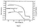
- the polyacene may be dissolved in a binder resin (for example poly( ⁇ -methylstyrene) and deposited (for example by spin coating), to form an organic semiconducting layer yielding a high charge mobility, of for example 0.5-1.5 cm 2 V 1 s -1 .
- a binder resin for example poly( ⁇ -methylstyrene)
- deposited for example by spin coating
- an organic semiconducting layer formulation for use in an organic field effect transistor comprising a compound selected from Compound groups 8 to 9 more preferably group 8; a binder; and optionally a solvent.
- an organic semiconducting layer formulation for use in an organic field effect transistor comprising a compound of Formula 1; a binder; and a solvent, wherein the binder is selected from poly( ⁇ -methylstyrene), TopasTM 8007, poly(4-methylstyrene), polystyrene and polystyrene-co- ⁇ -methylstyrene, most preferably poly( ⁇ -methylstyrene); and the solvent is selected from toluene, ethylcyclohexane, anisole and p-xylene; most preferably toluene.
- the binder is selected from poly( ⁇ -methylstyrene), TopasTM 8007, poly(4-methylstyrene), polystyrene and polystyrene-co- ⁇ -methylstyrene, most preferably poly( ⁇ -methylstyrene); and the solvent is selected from toluene, ethylcyclohexane,
- an organic semiconducting layer formulation for use in an organic field effect transistor comprising a compound of Formula 2; a binder; and a solvent, wherein the binder is selected from poly( ⁇ -methylstyrene), polyvinylcinnamate, and poly(4-vinylbiphenyl), most preferably poly( ⁇ -methylstyrene); and the solvent is 1,2-dichlorobenzene.
- an organic semiconducting layer formulation for use in an organic field effect transistor comprising a compound of Formula 3; a binder; and a solvent, wherein
- an organic semiconducting layer formulation of high mobility is obtained by combining a polyacene with a binder
- the resulting formulation leads to several other advantages.
- the polyacenes since they are soluble they may be deposited in a liquid form, for example from solution.
- the binder With the additional use of the binder it has now been found that the formulation may be coated onto a large area in a highly uniform manner. Without the use of binders the polyacene cannot be spin coated onto large areas as it does not result in uniform films.
- spin and drop-casting of a pure polyacene layer may in some cases result in relatively high mobility but it is difficult to provide a large area film with a constant mobility over the entire substrate which is a specific requirement for electronic devices.
- a binder when used in the formulation it is possible to control the properties of the formulation to adjust to printing processes, for example viscosity, solid content, surface tension. Whilst not wishing to be bound by any particular theory it is also anticipated that the use of a binder in the formulation fills in volume between crystalline grains otherwise being void, making the organic semiconducting layer less sensitive to air and moisture. For example, layers formed according to the first aspect of the present invention show very good stability in OFET devices in air.
- the invention also provides an organic semiconducting layer which comprises the organic semiconducting layer formulation.
- the invention further provides a process for preparing the organic semiconducting layer which comprises:
- the invention additionally provides an electronic device comprising the said organic semiconducting layer.
- the electronic device may include, without limitation, an organic field effect transistor (OFET), organic light emitting diode (OLED), photodetector, sensor, logic circuit, memory element, capacitor or photovoltaic (PV) cell.
- OFET organic field effect transistor
- OLED organic light emitting diode
- PV photovoltaic
- the active semiconductor channel between the drain and source in an OFET may comprise the layer of the invention.
- a charge (hole or electron) injection or transport layer in an OLED device may comprise the layer of the invention.
- the formulations according to the present invention and layers formed therefrom have particular utility in OFETs especially in relation to the preferred embodiments described herein.
- Compound Group 8 is represented by Formula 8:
- R 1 , R 2 , R 3 , R 4 , R 8 , R 9 , R 10 , R 11 , R 15 , R 16 and R 17 are each independently the same or different.
- R 1 , R 2 , R 3 , R 4 , R 8 , R 9 , R 10 and R 11 each independently comprises H, optionally substituted C 1-40 carbyl or hydrocarbyl groups, for example optionally substituted alkenyl, alkyaryl, aryl etc groups or halo groups for example F, Cl, Br.
- R 1 , R 2 , R 3 , R 4 , R 8 , R 9 , R 10 and R 17 comprise optionally substituted C 1-10 -alkyl groups for example methyl, ethyl, propyl, butyl, pentyl etc., most preferably methyl; halogen, for example F, Cl, Br most preferably F, or R 2 , and R 3 and R 9 and R 10 together with the carbon atoms to which they are attached form a C 4 -C 40 saturated or unsaturated ring, more preferably an optionally substituted C 4 -C 10 saturated or unsaturated ring, intervened by one or more oxygen or sulphur atoms or a group represented by formula -N(R a ), wherein R a is a hydrogen atom or a hydrocarbon group.
- R 15 , R 16 and R 17 may each independently be the same or different, preferably R 15 , R 16 and R 17 are the same and comprise an optionally substituted C 1 -C 40 carbyl or hydrocarbyl group, for example a C 1 -C 40 alkyl group (preferably C 1 -C 4 alkyl and most preferably methyl, ethyl, n-propyl or isopropyl) which may optionally be substituted for example with a halogen atom; a C 6 -C 40 aryl group (preferably phenyl) which may optionally be substituted for example with a halogen atom; a C 6 -C 40 arylalkyl group which may optionally be substituted for example with a halogen atom; a C 1 -C 40 alkoxy group which may optionally be substituted for example with a halogen atom; or a C 6 -C 40 arylalkyloxy group which may be a C 1 -C 40 alky
- R 15 , R 16 and R 17 are each independently selected from optionally substituted C 1-10 alkyl (more preferably C 1-4 and even more preferably C 1-3 alkyl, for example isopropyl) and optionally substituted C 6-10 aryl (preferably phenyl).
- X is preferably Silicon or Germanium, most preferably silicon.
- R 15 , R 16 and R 17 are preferably the same group as each other, for example the same optionally substituted alkyl group, as in triisopropylsilyl.
- the groups R 15 , R 16 and R 17 are the same optionally substituted C 1-10 (more preferably C 1-4 and even more preferably C 1-3 ) alkyl group.
- a preferred alkyl group in this case is isopropyl.
- a silyl group of formula -Si(R 15 )(R 16 )(R 17 ) as described above is a preferred optional substituent for the C 1 -C 40 carbyl or hydrocarbyl group etc.
- R 2 , R 3 , R 9 and R 10 are C 1-10 -alkyl
- one or more of R 2 , R 3 , R 9 and R 10 are preferably methyl, or one or more of R 1 , R 2 , R 3 , R 4 , R 8 , R 9 , R 10 and R 11 is F.
- R 1 , R 2 , R 3 , R 4 , R 8 , R 9 , R 10 and R 11 are each H.
- R 15 , R 16 and R 17 are C 1-10 -alkyl, more preferably C 1-5 -alkyl for example, methyl, ethyl or propyl.
- any two or more of the substituents which are located on adjacent ring positions of the polyacene may, together with the adjacent ring postion to which they are attached, optionally constitute a further aromatic or heterocyclic ring system fused to the polyacene compound.
- An example of this type of Group 8 pentacene compound is illustrated below in Group 8, example 6, wherein each pair of adjacent substituents R 1 and R 2 , R 3 and R 4 , R 8 and R 9 , and R 10 and R 11 constitute a benzene ring fused to the pentacene:
- one or more of the ring positions on the pentacene derivative other than the 1, 2, 3, 4, 6, 8, 9, 10, 11 and 13 positions may be substituted, but preferably they are unsubstituted, that is, they are occupied by hydrogen.
- Compound Group 9 is represented by Formula 9:
- R 2 , R 3 , R 7 , R 8 , R 15 , R 16 and R 17 are each independently the same or different and each independently comprise H, or optionally substituted C 1 -C 40 -carbyl or hydrocarbyl groups.
- R 2 and R 3 may be the same or different but are preferably the same substituent as each other.
- R 7 and R 8 may also be the same or different but are preferably the same substituent as each other.
- R 2 , R 3 , R 7 and R 8 are the same substituent as each other.
- R 2 and R 3 and R 7 and R 8 together with the carbon atom to which they are attached form a C 4 -C 40 saturated or unsaturated ring, more preferably a C 4 -C 10 saturated or unsaturated ring intervened by one or more oxygen or sulphur atoms or a group represented by the formula -N(R a ) wherein R a is a hydrogen atom or a hydrocarbon group, thereby forming a pseudo-pentacene compound.
- Preferred pseudo-pentacene derivatives of Compound Group 9 are as shown in Formula 9a and Formula 9b and isomers thereof, wherein one or more of the carbon atoms of the polyacene skeleton may be substituted by a heteroatom selected from N, P, As, O, S, Se and Te, preferably N or S.
- R 19 and R 20 are preferably the same substituent and comprise optionally substituted C 1-40 carbyl or hydrocarbyl groups. More preferably R 19 and R 20 each independently comprise optionally substituted, optionally unsaturated C 1-40 carbyl or hydrocarbyl groups, for example, optionally substituted alkyl, alkenyl, alkynyl, aryl or aralkyl groups or R 19 and R 20 either together with the carbon atoms to which they are attached or independently in combination with a substituent on a suitably adjacent atom from an optionally substituted C 4 -C 40 saturated or unsaturated ring optionally intervened by one or more oxygen or sulphur atoms or a group represented by Formula -N(R a ) wherein R a is a hydrogen atom or a hydrocarbon group.
- R 19 and R 20 are the same substituent and comprise hydrogen or a saturated or unsaturated C 1-4 -alkyl group for example methyl, ethyl, propyl, or butyl, most preferably R 19 and R 20 are each independently a methyl group or a hydrogen atom.
- R 15 , R 16 , R 17 may be the same or different, most preferably R 15 , R 16 and R 17 are the same and are as described in relation to compounds of Formula 8 above.
- one or more of the ring positions on the compound may be substituted, for example in order to form additional optionally substituted rings but preferably the other ring positions are unsubstituted, that is they are occupied by hydrogen.
- the C 1 -C 40 carbyl or hydrocarbyl group may be a saturated or unsaturated acyclic group, or a saturated or unsaturated cyclic group. Unsaturated acyclic or cyclic groups are preferred, especially alkenyl and alkynyl groups (especially ethynyl). Where the C 1 -C 40 carbyl or hydrocarbyl group is acyclic, the group may be linear or branched.
- the C 1 -C 40 carbyl or hydrocarbyl group includes for example: a C 1 -C 40 alkyl group, a C 2 -C 40 alkenyl group, a C 2 -C 40 alkynyl group, a C 3 -C 40 allyl group, a C 4 -C 40 alkyldienyl group, a C 4 -C 40 polyenyl group, a C 6 -C 18 aryl group, a C 6 -C 40 alkylaryl group, a C 6 -C 40 arylalkyl group, a C 4 -C 40 cycloalkyl group, a C 4 -C 40 cycloalkenyl group, and the like.
- Preferred among the foregoing groups are a C 1 -C 20 alkyl group, a C 2 -C 20 alkenyl group, a C 2 -C 20 alkynyl group, a C 3 -C 20 allyl group, a C 4 -C 20 alkyldienyl group, a C 6 -C 12 aryl group and a C 4 -C 20 polyenyl group, respectively; more preferred are a C 1 -C 10 alkyl group, a C 2 -C 10 alkenyl group, a C 2 -C 10 alkynyl group (especially ethynyl), a C 3 -C 10 allyl group, a C 4 -C 10 alkyldienyl group, a C 6 -C 12 aryl group and a C 4 -C 10 polyenyl group, respectively; and most preferred is C 2-10 alkynyl.
- alkyl group examples are, without limitation, methyl, ethyl, propyl, n-butyl, t-butyl, dodecanyl, trifluoromethyl, perfluoro-n-butyl, 2,2,2-trifluoroethyl, benzyl, 2-phenoxyethyl, etc.
- alkynyl group examples are ethynyl and propynl.
- aryl group are, without limitation, phenyl, 2-tolyl, 3-tolyl, 4-tolyl, naphthyl, biphenyl, 4-phenoxyphenyl, 4-fluorophenyl, 3-carbomethoxyphenyl, 4-carbomethoxyphenyl, etc.
- alkoxy group examples are, without limitation, methoxy, ethoxy, 2-methoxyethoxy, t-butoxy, etc.
- aryloxy group examples are, without limitation, phenoxy, naphthoxy, phenylphenoxy, 4-methylphenoxy, etc.
- amino group examples are, without limitation, dimethylamino, methylamino, methylphenylamino, phenylamino, etc.
- the optional substituents on the said C 1 -C 40 carbyl or hydrocarbyl groups for R 1 etc. preferably are selected from: silyl, sulpho, sulphonyl, formyl, amino, imino, nitrilo, mercapto, cyano, nitro, halo, C 1-4 alkyl, C 6-12 aryl, C 1-4 alkoxy, hydroxy and/or all chemically possible combinations thereof. More preferable among these optional substituents are silyl and C 6-12 aryl and most preferable is silyl.
- the silyl group in this specification may be shown by formula: -Si(R 15 )(R 16 )(R 17 ), wherein each of R 15 , R 16 and R 17 , which may be the same or different, independently represents hydrogen, a C 1 -C 40 -alkyl group (preferably C 1 -C 4 -alkyl and most preferably methyl, ethyl, n-propyl or isopropyl) which may optionally be substituted for example with a halogen atom; a C 6 -C 40 -aryl group (preferably phenyl) which may optionally be substituted for example with a halogen atom; a C 6 -C 40 -aralalkyl group which may optionally be substituted for example with a halogen atom; a C 1 -C 40 -alkoxy group which may optionally be substituted for example with a halogen atom; or a C 6 -C 40 -
- R 15 , R 16 and R 17 are each independently selected from optionally substituted C 1-10 -alkyl (more preferably C 1-4 and even more preferably C 1-3 -alkyl, for example isopropyl) and optionally substituted C 6-10 -aryl (preferably phenyl).
- R 15 , R 16 and R 17 are preferably the same group as each other, for example the same optionally substituted alkyl group, as in triisopropylsilyl.
- the groups R 15 , R 16 and R 17 are the same optionally substituted C 1-10 (more preferably C 14 and even more preferably C 1-3 ) alkyl group.
- a preferred alkyl group in this case is isopropyl.
- a silyl group of formula -Si(R 15 )(R 16 )(R 17 ) as described above is a preferred optional substituent for the C 1 -C 40 -carbyl or hydrocarbyl group etc.
- silyl group -Si(R 15 )(R 16 )(R 17 ) are, without limitation, trimethylsilyl, triethylsilyl, tripropylsilyl, dimethylethylsilyl, diethylmethylsilyl, dimethylpropylsilyl, dimethylisopropylsilyl, dipropylmethylsilyl, diisopropylmethylsilyl, dipropylethylsilyl, diisopropylethylsilyl, diethylisopropylsilyl, triisopropylsilyl, trimethoxysilyl, triethoxysilyl, triphenylsilyl, diphenylisopropylsilyl, diisopropylphenylsilyl, diphenylethylsilyl, diethylphenylsilyl, diphenylmethylsilyl, triphenoxysilyl, dimethylmethoxysilyl,
- Pentacene compounds according to the present invention are those of Compound Groups 8 and 9, more especially preferred are compound groups 8. Examples of these compounds include without limitation: 6,13-bis(trimethylsilylethynyl)pentacene, 6,13-bis(triethylsilylethynyl)pentacene, 6,13-bis(tripropylsilylethynyl)pentacene, 6,13-bis(dimethylethylsilylethynyl)pentacene, 6,13-bis(diethylmethylsilylethynyl)pentacene, 6,13-bis(dimethylpropylsilylethynyl)pentacene, 6,13-bis(dimethylisopropylsilylethynyl)pentacene, 6,13-bis(dipropylmethylsilylethynyl)-pentacene, 6,13-bis(diisopropylmethyls
- compounds of Group 8 and 9 include without limitation: 2,3,9,10-tetramethyl-6,13-bis(triisopropylsilylethynyl)pentacene, 5,11-bis(triisopropylsilyl ethynyl)anthra[2,3- b :6,7- b ]dithiophene, 5,11-bis(triisopropylsilylethynyl)anthra[2,3- b :7,6- b ] dithiophene, 1,8-difluoro-6,13-bis(triisopropylsilylethynyl)pentacene, 1,11-difluoro-6,13-bis(triisopropylsilylethynyl)pentacene and 2,3,9,10-tetrafluoro-6,13-bis(triisopropylsilyl ethynyl) pentacene.
- each R' is independently selected from silyl, which may both optionally be substituted.
- both R' is silyl, wherein the silyl group is preferably defined as above, that is, a silyl group of formula - Si(R 15 )(R 16 )(R 17 ).
- These latter highly preferred compounds thus have Formulae 1A' , 8A' and 88':
- R 15 , R 16 and R 17 in Formulae 1A', 8A' and 8B' are preferably the same as each other, for example the same alkyl group, as in 6,13-bis-(triisopropylsilylethynyl)pentacene.
- R 15 , R 16 and R 17 are preferably the same C 1-10 (preferably C 1-4 and more preferably C 1-3 ) alkyl group which may optionally be substituted.
- Optionally substituted isopropyl is a preferred alkyl group for such embodiments.
- At least one of R 15 , R 16 and R 17 contains an optionally substituted aryl (preferably phenyl) group.
- R 15 , R 18 and R 17 may be an optionally substituted C 6-18 aryl (preferably phenyl) group, an optionally substituted C 6-18 aryloxy (preferably phenoxy) group, an optionally substituted C 6-20 arylalkyl (for example benzyl) group, or an optionally substituted C 6-20 arylalkyloxy (for example benzyloxy) group.
- the remaining groups, if any, among R 15 , R 16 and R 17 are preferably C 1-10 (more preferably C 1-4 ) alkyl groups which may be optionally substituted.
- Ar represents an aryl-containing group for example an optionally substituted C 6-18 aryl group, an optionally substituted C 6-18 aryloxy group, an optionally substituted C 6-20 arylalkyl group or an optionally substituted C 6-20 arylalkyloxy group:
- R 15 and R 17 are preferably the same group as each other, for example an isopropyl group.
- Examples of compounds of Formulae 1C include, without limitation: 6,13-bis(triphenylsilylethynyl)pentacene, 6,13-bis(diphenylisopropylsilylethynyl)pentacene, 6,13-bis(diisopropylphenylsilylethynyl)pentacene, 6,13-bis(diphenylethylsilylethynyl)-pentacene, 6,13-bis(diethylphenyisilylethynyl)pentacene, 6,13-bis(diphenylmethylsilylethynyl)pentacene, 6,13-bis(triphenoxysilylethynyl)pentacene, 6,13-bis(dimethylphenoxysilylethynyl)pentacene, 6,13-bis(methylmethoxyphenylethynyl)-pentacene, 5,14-bis(tri
- the semiconducting polyacene has a field effect mobility, ⁇ , of more than 10 -5 cm 2 V -1 s -1 , preferably of more than 10 -4 cm 2 V -1 s -1 , more preferably of more than 10 -3 cm 2 V -1 s -1 , still more preferably of more than 10 -2 cm 2 V -1 s -1 and most preferably of more than 10 -1 cm 2 V -1 s -1 .
- the binder which is a polymer, may comprise either an insulating binder or a semiconducting binder, or mixtures thereof may be referred to herein as the organic binder, the polymeric binder or simply the binder.
- Preferred binders according to the present invention are materials of low permittivity, that is, those having a permittivity, ⁇ at 1,000 Hz of 3.3 or less.
- the organic binder preferably has a permittivity at 1,000 Hz of less than 3.0, more preferably 2.9 or less.
- the organic binder has a permittivity at 1,000 Hz of greater than 1.7. It is especially preferred that the permittivity of the binder is in the range from 2.0 to 2.9.
- the use of binders with a permittivity of greater than 3.3 at 1,000Hz may lead to a reduction in the OSC layer mobility in an electronic device, for example an OFET.
- high permittivity binders could also result in increased current hysteresis of the device, which is undesirable.
- An example of a suitable organic binder is polystyrene. Further examples are given below.
- the organic binder is one in which at least 95%, more preferably at least 98% and especially all of the atoms consist of hydrogen, fluorine and carbon atoms.
- the binder normally contains conjugated bonds especially conjugated double bonds and/or aromatic rings.
- the binder should preferably be capable of forming a film, more preferably a flexible film.
- Polymers of styrene and alpha-methyl styrene, for example copolymers including styrene, alpha-methylstyrene and butadiene may suitably be used.
- Binders of low permittivity of use in the present invention have few permanent dipoles which could otherwise lead to random fluctuations in molecular site energies.
- the permittivity (dielectric constant) can be determined by the ASTM D150 test method.
- binders are used which have solubility parameters with low polar and hydrogen bonding contributions as materials of this type have low permanent dipoles.
- a preferred range for the solubility parameters of a binder for use in accordance with the present invention is provide in Table 1 below. Table 1 Hansen parameter ⁇ d MPa 1/2 ⁇ p MPa 1/2 ⁇ h MPa 1/2 Preferred range 14.5+ 0-10 0-14 More preferred range 16+ 0-9 0-12 Most preferred range 17+ 0-8 0-10
- the three dimensional solubility parameters listed above include: dispersive ( ⁇ d ), polar ( ⁇ p ) and hydrogen bonding ( ⁇ h ) components (C.M. Hansen, Ind. Eng. and Chem., Prod. Res. and Devl., 9, No3, p282., 1970). These parameters may be determined empirically or calculated from known molar group contributions as described in Handbook of Solubility Parameters and Other Cohesion Parameters ed. A.F.M. Barton, CRC Press, 1991. The solubility parameters of many known polymers are also listed in this publication.
- the permittivity of the binder has little dependence on frequency. This is typical of non-polar materials.
- Polymers and/or copolymers can be chosen as the binder by the permittivity of their substituent groups.
- a list of low polarity binders suitable for use in the present invention is given (without limiting to these examples) in Table 2 : Table 2 Binder typical low frequency permittivity ⁇ Polystyrene 2.5 poly( ⁇ -methylstyrene) 2.6 poly( ⁇ -vinylnaphtalene) 2.6 poly(vinyltoluene) 2.6 Polyethylene 2.2-2.3 cis-polybutadiene 2.0 Polypropylene 2.2 Polyisoprene 2.3 poly(4-methyl-1-pentene) 2.1 poly (4-methylstyrene) 2.7 poly(chorotrifluoroethylene) 2.3-2.8 poly(2-methyl-1,3-butadiene) 2.4 poly(p-xylylene) 2.6 poly( ⁇ - ⁇ - ⁇ '- ⁇
- binders include : poly(1,3-butadiene) or polyphenylene.
- Copolymers containing the repeat units of the above polymers are also suitable as binders. Copolymers offer the possibility of improving compatibility with the polyacene, modifying the morphology and/or the glass transition temperature of the final layer composition. It will be appreciated that in the above table certain materials are insoluble in commonly used solvents for preparing the layer. In these cases analogues can be used as copolymers. Some examples of copolymers are given in Table 3 (without limiting to these examples). Both random or block copolymers can be used. It is also possible to add some more polar monomer components as long as the overall composition remains low in polarity.
- Binder typical low frequency permittivity Poly(ethylene/tetrafluoroethylene) 2.6 poly(ethylene/chlorotrifluoroethylene) 2.3 fluorinated ethylene/propylene copolymer 2-2.5 polystyrene-co- ⁇ -methylstyrene 2.5-2.6 ethylene/ethyl acrylate copolymer 2.8 poly(styrene/10%butadiene) 2.6 poly(styrene/15%butadiene) 2.6 poly(styrene/2,4 dimethylstyrene) 2.5 Topas TM (all grades) 2.2-2.3
- copolymers may include: branched or non-branched polystyrene-block-polybutadiene, polystyrene-block(polyethylene-ran-butylene)-block-polystyrene, polystyrene-block-polybutadiene-block-polystyrene, polystyrene-(ethylene-propylene)-diblock-copolymers (e.g. KRATON®-G1701E, Shell), poly(propylene-co-ethylene) and poly(styrene-co-methylmethacrylate).
- polystyrene-block-polybutadiene polystyrene-block(polyethylene-ran-butylene)-block-polystyrene, polystyrene-block-polybutadiene-block-polystyrene, polystyrene-(ethylene-propylene)-diblock-copolymers (e.g
- Preferred insulating binders for use in the organic semiconductor layer formulation according to the present Invention are poly( ⁇ -methylstyrene), polyvinylcinnamate, poly(4-vinylbiphenyl), poly(4-methylstyrene), and Topas TM 8007.
- the most preferred insulating binders are poly( ⁇ -methylstyrene), polyvinylcinnamate and poly(4-vinylbiphenyl).
- the organic binder may itself be a semiconductor, where it will be referred to herein as a semiconducting binder.
- the semiconducting binder is still preferably a binder of low permittivity as herein defined.
- Semiconducting binders for use in the present invention preferably have a number average molecular weight (M n ) of at least 1500-2000, more preferably at least 3000, even more preferably at least 4000 and most preferably at least 5000.
- the semiconducting binder preferably has a charge carrier mobility, ⁇ , of at least 10 -5 cm 2 V -1 s -1 , more preferably at least 10 -4 cm 2 V -1 s -1 .
- a preferred class of semiconducting binder has repeat units of Formula 10: wherein Ar 1 , Ar 2 and Ar 3 , which may be the same or different, each represent, independently if in different repeat units, an optionally substituted aromatic group (mononuclear or polynuclear) and in the semiconductor binder n is an integer of at least 6, preferably at least 10, more preferably at least 15 and most preferably at least 20.
- a mononuclear aromatic group has only one aromatic ring, for example phenyl or phenylene.
- a polynuclear aromatic group has two or more aromatic rings which may be fused (for example napthyl or naphthylene), individually covalently linked (for example biphenyl) and/or a combination of both fused and individually linked aromatic rings.
- each Ar 1 , Ar 2 and Ar 3 is an aromatic group which is substantially conjugated over substantially the whole group.
- Examples of monomer units A, B,...Z include units of Formula 10 and Formulae 12 to 17 given below: wherein R1 and R2 may be independently: H; optionally substituted alkyl; alkoxy; thioalkyl; acyl; optionally substituted aryl; a fluorine atom; a cyano group; a nitro group; an optionally substituted secondary or tertiary alkylamine or arylamine of formula -N(R a )(R b ), wherein R a and R b may each be independently represented by H, optionally substituted alkyl, aryl, optionally substituted aryl, alkoxy or polyalkoxy groups; or other substituent and - is any terminal or end capping group including hydrogen, (the alkyl and aryl groups may be optionally fluorinated); in which X may be Se, Te, O, S or -N(R c ) more preferably X is O, S or -N(R c )
- the polymers may be terminated by any terminal group, that is any end-capping or leaving group, including hydrogen.
- each monomer A, B,...Z may be a conjugated oligomer or polymer comprising a number, for example 2 to 50, of the units of Formulae 12-17.
- the semiconducting binder preferably includes: arylamine, fluorene, thiophene, spiro bifluorene and/or optionally substituted aryl (for example, phenylene) groups, more preferably arylamine, still more preferably triarylamine groups.
- aryl for example, phenylene
- the aforementioned groups may be linked by further conjugating groups for example vinylene.
- the semiconducting binder comprises a polymer (either a homo-polymer or copolymer, including block-copolymer) containing one or more of the aforementioned arylamine, fluorene, thiophene and/or optionally substituted aryl groups.
- a preferred semiconducting binder comprises a homo-polymer or copolymer (including block-copolymer) containing arylamine (preferably triarylamine) and/or fluorene units.
- Another preferred semiconducting binder comprises a homo-polymer or co-polymer (including block-copolymer) containing fluorene and/or thiophene units.
- the semiconducting binder may also contain: carbazole, stilbene repeat units.
- carbazole for example polyvinylcarbazole or polystilbene polymers, copolymers may be used.
- the semiconducting binder may optionally contain polyacene segments (for example repeat units as described for Formula A above) to improve compatibility with the soluble polyacene molecules.
- the most preferred semiconducting binders for use in the organic semiconductor layer formulation according to the present invention are poly(9-vinylcarbazole) and PTAA1.
- the semiconducting binder For application of the semiconducting layer in p-channel FETs, it is desirable that the semiconducting binder should have a higher ionisation potential than the polyacene semiconductor, otherwise the binder may form hole traps. In n-channel materials the semiconducting binder should have lower electron affinity than the n-type semiconductor to avoid electron trapping.
- the formulation according to the present invention may be prepared by a process which comprises:
- the binder may be formed In situ by mixing or dissolving a polyacene in a precursor of a binder, for example a liquid monomer, oligomer or crosslinkable polymer, optionally in the presence of a solvent, and depositing the mixture or solution, for example by dipping, spraying, painting or printing it, on a substrate to form a liquid layer and then curing the liquid monomer, oligomer or crosslinkable polymer, for example by exposure to radiation, heat or electron beams, to produce a solid layer.
- a precursor of a binder for example a liquid monomer, oligomer or crosslinkable polymer, optionally in the presence of a solvent
- depositing the mixture or solution for example by dipping, spraying, painting or printing it, on a substrate to form a liquid layer and then curing the liquid monomer, oligomer or crosslinkable polymer, for example by exposure to radiation, heat or electron beams, to produce a solid layer.
- a preformed binder it may be dissolved together with the polyacene in a suitable solvent, and the solution deposited for example by dipping, spraying, painting or printing it on a substrate to form a liquid layer and then removing the solvent to leave a solid layer.
- solvents are chosen which are able to dissolve both the binder and polyacene, and which upon evaporation from the solution blend give a coherent defect free layer.
- Suitable solvents for the binder or polyacene can be determined by preparing a contour diagram for the material as described in ASTM Method D 3132 at the concentration at which the mixture will be employed. The material is added to a wide variety of solvents as described in the ASTM method.
- the formulation may comprise one or more polyacene compounds and/or one of more binders and that the process for preparing the formulation may be applied to such formulations.
- organic solvents which may be considered are: CH 2 Cl 2 , CHCl 3 , monochlorobenzene, o-dichlorobenzene, tetrahydrofuran, anisole, morpholine, toluene, o-xylene, m-xylene, p-xylene, 1,4-dioxane, acetone, methylethylketone, 1,2-dichloroethane, 1,1,1-trichloroethane, 1,1,2,2-tetrachloroethane, ethyl acetate, n-butyl acetate, dimethylformamide, dimethylacetamide, dimethylsulfoxide, tetralin, decalin and/or mixtures thereof.
- solutions are evaluated as one of the following categories: complete solution, borderline solution or insoluble.
- the contour line is drawn to outline the solubility parameter-hydrogen bonding limits dividing solubility and insolubility.
- Solvent blends may also be used and can be identified as described in " Solvents, W.H.Ellis, Federation of Societies for Coatings Technology, p9-10, 1986 ". Such a procedure may lead to a blend of 'non' solvents that will dissolve both the binder and polyacene, although it is desirable to have at least one true solvent in a blend.
- Preferred solvents for use in the organic semiconducting layer formulation according to the present invention for use with both insulating and semiconducting binders and mixtures thereof are: xylene(s), toluene, tetralin and o-dichlorobenzene.
- the proportions of binder to polyacene in the formulation or layer according to the present invention are typically 20:1 to 1:20 by weight, preferably 10:1 to 1:10 more preferably 5:1 to 1:5, still more preferably 3:1 to 1:3 further preferably 2:1 to 1:2 and especially 1:1.
- dilution of the polyacene in the binder has been found to have little or no detrimental effect on the charge mobility, in contrast to what would have been expected from the prior art.
- the level of the solids content in the organic semiconducting layer formulation is also a factor in achieving improved mobility values for electronic devices such as OFETs.
- the solids content of the formulation is preferably 0.1 to 10% by weight, more preferably 0.5 to 5% by weight.
- Patterning of the layer of the invention may be carried out by photolithography or electron beam lithography.
- Liquid coating of organic electronic devices is more desirable than vacuum deposition techniques.
- the polyacene and binder mixtures of the present invention enable the use of a number of liquid coating techniques.
- the organic semiconductor layer may be incorporated into the final device structure by, for example and without limitation, dip coating, spin coating, ink jet printing, letter-press printing, screen printing, doctor blade coating; roller printing, reverse-roller printing; offset lithography printing, flexographic printing, web printing, spray coating, brush coating or pad printing.
- the present invention is particularly suitable for use in spin coating the organic semiconductor layer into the final device structure.
- Selected polyacene and binder compositions of the present invention may be applied to prefabricated device substrates by ink jet printing or microdispensing.
- industrial piezoelectric print heads such as but not limited to those supplied by Aprion, Hitachi-Koki, InkJet Technology, On Target Technology, Picojet, Spectra, Trident, Xaar may be used to apply the organic semiconductor layer to a substrate.
- semi-industrial heads such as those manufactured by Brother, Epson, Konica,. Seiko Instruments Toshiba TEC or single nozzle microdispensers such as those produced by Microdrop and Microfab may be used.
- solvents In order to be applied by ink jet printing or microdispensing, polyacene and binder compositions must first be dissolved in a suitable solvent. Solvents must fulfil the requirements stated above and must not have any detrimental effect on the chosen print head. Additionally, solvents should have boiling points >100°C, preferably >140°C and more preferably >150°C in order to prevent operability problems caused by the solution drying out inside the print head.
- Suitable solvents include substituted and non-substituted xylene derivatives, di-C 1-2 alkyl formamide, substituted and non-substituted anisoles and other phenol-ether derivatives, substituted heterocycles such as substituted pyridines, pyrazines, pyrimidines, pyrrolidinones, substituted and non-substituted N,N -di-C 1-2 -alkylanilines and other fluorinated or chlorinated aromatics.
- a preferred solvent for depositing a binder/polyacene formulation by ink jet printing comprises a benzene derivative which has a benzene ring substituted by one or more substituents wherein the total number of carbon atoms among the one or more substituents is at least three.
- the benzene derivative may be substituted with a propyl group or three methyl groups, in either case there being at least three carbon atoms in total.
- Such a solvent enables an ink jet fluid to be formed comprising the solvent with the binder and polyacene which reduces or prevents clogging of the jets and separation of the components during spraying.
- the solvent(s) may include those selected from the following list of examples: dodecylbenzene; 1-Methyl-4-tert-butylbenzene; Terpineol; Limonene; lsodurene; Terpinolene; Cymene; Diethylbenzene.
- the solvent may be a solvent mixture, that is a combination of two or more solvents, each solvent preferably having a boiling point >100°C, more preferably >140°C. Such solvent(s) also enhance film formation in the layer deposited and reduce defects in the layer.
- the ink jet fluid (that is mixture of solvent, binder and polyacene) preferably has a viscosity at 20°C of 1-100mPa.s, more preferably 1-50mPa.s and most preferably 1-30mPa.s
- binder in the present invention also allows the viscosity of the coating solution to be tuned to meet the requirements of the particular print head.
- the exact thickness of the layer will depend, for example, upon the requirements of the electronic device in which the layer is used. For use in an OFET or OLED, the layer thickness may typically be 500 nm or less.
- the semiconducting layer of the present invention there may be used two or more different polyacene compounds of Formula 1-9. Additionally or alternatively, in the semiconducting layer there may be used two or more organic binders of the present invention.
- the invention further provides a process for preparing the organic semiconducting layer which comprises (i) depositing on a substrate a liquid layer of a mixture which comprises a polyacene compound, an organic binder resin or precursor thereof and optionally a solvent, and (ii) forming from the liquid layer a solid layer which is the organic semiconducting layer.
- the solid layer may be formed by evaporation of the solvent and/or by reacting the binder resin precursor (if present) to form the binder resin in situ.
- the substrate may include any underlying device layer, electrode or separate substrate such as silicon wafer or polymer substrate for example.
- the binder may be alignable, for example capable of forming a liquid crystalline phase.
- the binder may assist alignment of the polyacene, for example such that the polyacene backbone is preferentially aligned along the direction of charge transport.
- Suitable processes for aligning the binder include those processes used to align polymeric organic semiconductors such as described in WO 03/007397 (Plastic Logic).
- the present invention also provides the use of the semiconducting formulation or layer in an electronic device.
- the formulation may be used as a high mobility semiconducting material in various devices and apparatus.
- the formulation may be used, for example, in the form of a semiconducting layer or film.
- the present invention provides a semiconducting layer for use in an electronic device, the layer comprising the formulation according to the invention.
- the layer or film may be less than about thirty microns. For various electronic device applications, the thickness may be less than about one micron thick.
- the layer may be deposited, for example on a part of an electronic device, by any of the aforementioned solution coating or printing techniques.
- the formulation may be used, for example as a layer or film, in a field effect transistor (FET) for example as the semiconducting channel, organic light emitting diode (OLED) for example as a hole or electron injection or transport layer or electroluminescent layer, photodetector, chemical detector, photovoltaic cell (PVs), capacitor sensor, logic circuit, display, memory device and the like.
- FET field effect transistor
- OLED organic light emitting diode
- PVs photovoltaic cell
- capacitor sensor logic circuit
- display memory device and the like.
- EP electrophotographic
- the formulation is preferably solution coated to form a layer or film in the aforementioned devices or apparatus to provide advantages in cost and versatility of manufacture.
- the improved charge carrier mobility of the formulation of the present invention enables such devices or apparatus to operate faster and/or more efficiently.
- the formulation and layer of the present invention are especially suitable for use in an organic field effect transistor OFET as the semiconducting channel. Accordingly, the invention also provides an organic field effect transistor (OFET) comprising a source electrode, a drain electrode and an organic semiconducting channel connecting the source and drain electrodes, wherein the organic semiconducting channel comprises an organic semiconducting layer according to the present invention.
- OFET organic field effect transistor
- Other features of the OFET are well known to those skilled in the art.
- each label and/or index can represent any of those groups listed independently from each other, independently within each repeat unit, independently within each Formula and/or independently on each group which is substituted as appropriate.
- groups for example R 5 ).
- optional groups may comprise all chemically possible combinations in the same group and/or a plurality (preferably two) of the aforementioned groups (for example amino and sulphonyl if directly attached to each other represent a sulphamoyl radical).
- Preferred optional substituents comprise: C 1-4 alkyl; methoxy and/or ethoxy (any of these optionally substituted by at least one halo); amino (optionally substituted by at least one methyl and/or ethyl); and/or halo.
- 'carbyl group' denotes any monovalent or multivalent organic radical moiety which comprises at least one carbon atom either without any non-carbon atoms (for example -C ⁇ C-), or optionally combined with at least one other non-carbon atom (for example alkoxy, carbonyl etc.).
- hydrocarbon group' 'hydrocarbyl' or the like may be used herein interchangeably.
- a hydrocarbon group may be optionally substituted.
- a hydrocarbon group may also contain at least one of the following heteroatom containing moieties: oxy, thio, sulphinyl, sulphonyl, amino, imino, nitrilo and/or combinations thereof.
- 'halo' as used herein signifies fluoro, chloro, bromo and iodo.
- a group herein which comprises a chain of three or more carbon atoms signifies a group in which the chain wholly or in part may be linear, branched and/or form a ring (including spiro and/or fused rings).
- Naphtho[2,1,8-qra]naphthacene-7,12-dione (1 molar equivalent (0.50g, 1.50mmol)) was then added and the reaction mixture allowed to warm up to room temperature with stirring overnight.
- a solution of 10% aqueous HCl saturated with SnCl 2 (10ml) was added at room temperature and the reaction mixture was stirred at 50°C for 30 minutes.
- 2M aqueous Na 2 CO 3 (5ml) was added and the resulting crude solution was filtered through celite and then concentrated under vacuum.
- test field effect transistor was manufactured by using a PEN substrate upon which were patterned Pt/Pd source and drain electrodes by standard techniques, for example shadow masking.
- Semiconductor formulations were prepared using compound 1 (example 12) and compound 4 (example 14) blended with an inert polymeric binder resin (poly(alpha-methylstyrene)(p- ⁇ MS)). The semiconductor formulations were then dissolved one part into 99 parts of solvent (toluene for examples 12 and 13, 1,2-dichlorobenzene for examples 14 and 15), and spin coated onto the substrate at 500 rpm for 18 seconds. To ensure complete drying, the samples were placed in an oven for 20 minutes at 100°C.
- films of the pure organic semiconductor compound (OSC) in the absence of binder were coated onto the substrates by spin coating (comparative example 13 for compound 1 and comparative example 15 for compound 4). These samples were then also dried in an oven for 20 minutes at 100°C.
- the insulator material (Cytop 107M, available from Asahi Glass) was mixed 3 parts to 2 parts of perfluorosolvent (FC75, Acros catalogue number 12380) and then spin-coated onto the semiconductor giving a thickness typically of approximately 1 ⁇ m.
- FC75 perfluorosolvent
- the samples were placed once more in an oven at 100°C for 20 minutes to evaporate solvent from the insulator.
- a gold gate contact was defined over the device channel area by evaporation through a shadow mask.
- the voltages applied to the transistor are relative to the potential of the source electrode.
- a negative potential is applied to the gate
- positive charge carriers are accumulated in the semiconductor on the other side of the gate dielectric.
- This is called the accumulation mode.
- the capacitance per unit area of the gate dielectric C I determines the amount of the charge thus induced.
- V DS negative potential
- the accumulated carriers yield a source-drain current I DS which depends primarily on the density of accumulated carriers and, importantly, their mobility in the source-drain channel. Geometric factors such as the drain and source electrode configuration, size and distance also affect the current.
- I DS ⁇ WC l L ⁇ V G - V 0 ⁇ V DS - V DS 2 2 + I ⁇ , where V 0 is an offset voltage and I ⁇ is an ohmic current independent of the gate voltage and is due to the finite conductivity of the material.
- V 0 is an offset voltage
- I ⁇ is an ohmic current independent of the gate voltage and is due to the finite conductivity of the material.
- the transistor sample was mounted in a sample holder. Microprobe connections were made to the gate, drain and source electrodes using Karl Suss PH100 miniature probe-heads. These were linked to a Hewlett-Packard 4155B parameter analyser. The drain voltage was set to -5 V and the gate voltage was scanned from +20 to -60V and back to +20V in 1 V steps. In accumulation, when
- the field effect mobility can be calculated from the gradient (S) of I DS vs. V G given by Equation 2.
- S ⁇ ⁇ WC i ⁇ V DS L
- OFETs were prepared using the method as described for examples 12 to 15 with the exception that different polymeric binders were used.
- Table 5 - Mobility measurements for OFETs prepared using a range of polymeric binders Example number Organic semi-conducting material (OSC) Binder mixed at 1:1 (by weight) with polyacene OSC & binder solids content in coating solution (by weight) Solvent Mobility [cm 2 /Vs] (+/-1 std.
- OSC Organic semi-conducting material
- OFETs were prepared using the method as described for examples 12 to 15 above with the exception that the polymeric binder used was a semiconducting material rather than an insulating binder. The results are illustrated in Table 6.
- Table 6 - Mobility measurements for OFETs prepared using a semiconducting binder Example number Organic semi-conducting material (OSC) Binder mixed at 1:1 (by weight) with polyacene OSC and binder solids content in coating solution (by weight) Solvent Mobility [cm 2 /Vs] (+/-1std.dev.) Sample size Permittivity of semiconducting binder ⁇ at 1 kHz 27
- Compound 4 poly(9-vinylcarbazol) 1% 1.2-Dichlorobenzene 1.44 ⁇ 0.35 7 2.7
- the poly(9-vinylcarbazol) is available from Aldrich, catalogue number:18,260-5 (exa
- OFETs were again prepared using the method as described for examples 12 to 15 above. However, in examples 29 to 31 the ratio of OSC material to binder was varied. Example 12 is also included for comparison. Table 7- Mobility measurements for OFETs prepared with varying Quantities of binder to OSC material Example number Organic Semiconducting Material (OSC) Binder OSC and binder solids content in coating solution (by weight) OSC : Binder Ratio (wt:wt) Mobility [cm 2 /Vs] Sample Size 12 Compound 1 p- ⁇ MS 1% 50:50 0.433 (+/-0.19) 9 29 Compound 1 p- ⁇ MS 1% 75:25 0.321 (+/-0.11) 7 30 Compound 1 p- ⁇ MS 1% 90:10 0.327 (+/- 0.11) 6 31 Compound 1 p- ⁇ MS 1% 95:5 0.244 (+/- 0.077) 8
- OSC Organic Semiconducting Material
- OFETs were again prepared using the method as described for examples 12 to 15 above with the exception that the solids content of the formulation was varied.
- Table 8 Variation of the solids content in a coating solution used to prepare an OFET Example number Organic semiconducting material (OSC) Binder mixed at 1:1 (by weight) with polyacene OSC and binder solids content in coating solution (by weight) Mobility [cm 2 /Vs] (+/-1 std.
- OSC Organic semiconducting material
Landscapes
- Chemical & Material Sciences (AREA)
- Materials Engineering (AREA)
- Engineering & Computer Science (AREA)
- Organic Chemistry (AREA)
- Physics & Mathematics (AREA)
- Spectroscopy & Molecular Physics (AREA)
- Polymers & Plastics (AREA)
- Health & Medical Sciences (AREA)
- Medicinal Chemistry (AREA)
- Chemical Kinetics & Catalysis (AREA)
- Thin Film Transistor (AREA)
- Compositions Of Macromolecular Compounds (AREA)
- Organic Low-Molecular-Weight Compounds And Preparation Thereof (AREA)
- Photovoltaic Devices (AREA)
- Light Receiving Elements (AREA)
- Heterocyclic Carbon Compounds Containing A Hetero Ring Having Oxygen Or Sulfur (AREA)
Claims (44)
- Organische Halbleiterschichtformulierung, welche enthält: ein organisches Bindemittel, welches eine Dielektrizitätskonstante, ε, bei 1000 Hz von 3,3 oder weniger besitzt; und eine Polyacenverbindung ausgewählt aus der durch Formel 8 dargestellten Verbindungsgruppe 8,
 worin R1, R2, R3, R4, R8, R9, R10, R11, R15, R16 und R17 in Gruppe 8 jeweils unabhängig gleich oder verschieden sind und jeweils unabhängig für H, eine gegebenenfalls substituierte C1-C40 Carbyl- oder Hydrocarbylgruppe oder eine Halogengruppe (Cl, Br, F) stehen; und worin A für Silicium oder Germanium steht,oder ausgewählt aus der durch Formel 9 dargestellten Verbindungsgruppe 9,
 worin R2, R3, R7, R8, R15, R16 und R17 in Gruppe 9 jeweils unabhängig gleich oder verschieden sind und jeweils unabhängig H oder gegebenenfalls substituierte C1-C40 Carbyl- oder Hydrocarbylgruppen enthalten und worin R2 und R3 und R7 und R8 zusammen mit dem Kohlenstoffatom, an das sie gebunden sind, einen C4-C40 gesättigten oder ungesättigten Ring bilden, wodurch eine Pseudo-Pentacenverbindung entsteht.
 - Organische Halbleiterschichtformulierung nach Anspruch 1, worin es sich bei der C1-C40 Carbyl- oder Hydrocarbylgruppe in den Polyacenen der Verbindungsgruppe 8 und 9 um eine C1-C40 Alkylgruppe, eine C2-C40 Alkenylgruppe, eine C2-C40 Alkinylgruppe, eine C3-C40 Allylgruppe, eine C4-C40 Alkyldienylgruppe, eine C4-C40 Polyenylgruppe, eine C6-C18 Arylgruppe, eine C6-C40 Alkylarylgruppe, eine C6-C40 Arylalkylgruppe, eine C4-C40 Cycloalkylgruppe oder eine C4-C40 Cycloalkenylgruppe handelt.
- Organische Halbleiterschichtformulierung nach einem beliebigen der vorhergehenden Ansprüche, worin es sich bei der C1-C40 Carbyl- oder Hydrocarbylgruppe in den Polyacenen der Verbindungsgruppe 8 und 9 um eine C1-C20 Alkylgruppe, eine C2-C20 Alkenylgruppe, eine C2-C20 Alkinylgruppe, eine C3-C20 Allylgruppe, eine C4-C20 Alkyldienylgruppe, eine C6-C12 Arylgruppe oder eine C4-C20 Polyenylgruppe handelt.
- Organische Halbleiterschichtformulierung nach einem beliebigen der vorhergehenden Ansprüche, worin es sich bei der C1-C40 Carbyl- oder Hydrocarbylgruppe in den Polyacenen der Verbindungsgruppe 8 und 9 um eine C1-C10 Alkylgruppe, eine C2-C10 Alkenylgruppe, eine C2-C10 Alkinylgruppe (insbesondere Ethinyl), eine C3-C10 Allylgruppe, eine C4-C10 Alkyldienylgruppe, eine C6-C12 Arylgruppe oder eine C4-C10 Polyenylgruppe handelt.
- Organische Halbleiterschichtformulierung nach einem beliebigen der vorhergehenden Ansprüche, worin die gegebenenfalls vorhandenen Substituenten an den C1-C40 Carbyl- oder Hydrocarbylgruppen ausgewählt sind aus: Silyl, Sulfo, Sulfonyl, Formyl, Amino, Imino, Nitrilo, Mercapto, Cyano, Nitro, Halogen, C1-4 Alkyl, C6-12 Aryl, C1-4 Alkoxy und Hydroxy.
- Organische Halbleiterschichtformulierung nach einem beliebigen der vorhergehenden Ansprüche, worin das Polyacen aus der durch Formel 8 dargestellten Verbindungsgruppe 8 ausgewählt ist,

- Organische Halbleiterschichtformulierung nach Anspruch 6, worin X Silicium bedeutet.
- Organische Halbleiterschichtformulierung nach Anspruch 6 oder 7, worin, wenn X Silicium bedeutet, das eine Silylgruppe bildet, R15, R16 und R17 die gleiche gegebenenfalls substituierte C1-10 Alkylgruppe bedeuten.
- Organische Halbleiterschichtformulierung nach einem beliebigen der Ansprüche 6 bis 8, worin R15, R16 und R17 aus C1-4 Alkyl ausgewählt sind.
- Organische Halbleiterschichtformulierung nach Anspruch 8 oder 9, worin, wenn R2, R3, R9 und R10 C1-10 Alkyl bedeuten, eines oder mehrere von R2, R3, R9 und R10 Methyl bedeuten.
- Organische Halbleiterschichtformulierung nach Anspruch 8 oder 9, worin eines oder mehrere von R1, R2, R3, R4, R8, R9, R10 und R11 F bedeuten.
- Organische Halbleiterschichtformulierung nach einem beliebigen der Ansprüche 6 bis 9, worin R1, R2, R3, R4, R8, R9, R10 und R11 jeweils H bedeuten.
- Organische Halbleiterschichtformulierung nach einem beliebigen der Ansprüche 1 bis 5, worin in der Verbindungsgruppe 9 R2 und R3 und R7 und R8 zusammen mit dem Kohlenstoffatom, an das sie gebunden sind, einen C4-C40 gesättigten oder ungesättigten Ring bilden, der durch ein oder mehrere Sauerstoff- oder Schwefelatome oder eine durch die Formel -N(Ra) dargestellte Gruppe, worin Ra ein Wasserstoffatom oder eine Kohlenwasserstoffgruppe bedeutet, unterbrochen ist, wodurch eine Pseudo-Pentacenverbindung entsteht.
- Organische Halbleiterschichtformulierung nach einem beliebigen der Ansprüche 1 bis 5 und 13, worin die Pseudo-Pentacenverbindung der Verbindungsgruppe 9 ausgewählt ist aus der Gruppe 9a und deren Isomeren

- Organische Halbleiterschichtformulierung nach Anspruch 14, worin R19 und R20 jeweils unabhängig gegebenenfalls substituierte Alkyl-, Alkenyl-, Alkinyl-, Aryl- oder Aralkylgruppen enthalten oder R19 und R20 entweder zusammen mit den Kohlenstoffatomen, an die sie gebunden sind, oder unabhängig in Kombination mit einem Substituenten an einem geeigneten benachbarten Atom einen gegebenenfalls substituierten C4-C40 gesättigten oder ungesättigten Ring bilden, der gegebenenfalls durch ein oder mehrere Sauerstoff- oder Schwefelatome oder eine durch die Formel -N(Ra) dargestellte Gruppe, worin Ra ein Wasserstoffatom oder eine Kohlenwasserstoffgruppe bedeutet, unterbrochen ist.
- Organische Halbleiterschichtformulierung nach Anspruch 14 oder 15, worin R19 und R20 den gleichen Substituenten bedeuten und Wasserstoff oder eine gesättigte oder ungesättigte C1-4 Alkylgruppe enthalten.
- Organische Halbleiterschichtformulierung nach einem beliebigen der Ansprüche 14 bis 16, worin R15, R16 und R17 gleich sind und wie für die Verbindungen der Formel 8 in einem beliebigen der Ansprüche 1 bis 9 definiert sind.
- Organische Halbleiterschichtformulierung nach einem beliebigen der vorhergehenden Ansprüche, worin das organische Bindemittelharz eine Dielektrizitätskonstante bei 1000 Hz von weniger als 3,0, vorzugsweise 2,9 oder weniger besitzt.
- Organische Halbleiterschichtformulierung nach Anspruch 19, worin das organische Bindemittelharz eine Dielektrizitätskonstante bei 1000 Hz von mehr als 1,7, insbesondere eine Dielektrizitätskonstante von 2,0 bis 2,9 besitzt.
- Organische Halbleiterschichtformulierung nach einem beliebigen der vorhergehenden Ansprüche, worin es sich bei dem organischen Bindemittelharz um ein isolierendes Bindemittel handelt.
- Organische Halbleiterschichtformulierung nach Anspruch 20, worin das isolierende Bindemittel ausgewählt ist aus Polystyrol, Poly(α-methylstyrol), Poly(α-vinylnaphthalin), Poly(vinyltoluol), Polyethylen, cis-Polybutadien, Polypropylen, Polyisopren, Poly(4-methyl-1-penten), Poly(4-methylstyrol), Poly(chlortrifluorethylen), Poly(2-methyl-1,3-butadien), Poly(p-xylylen), Poly(α-α-α'-α' tetrafluor-p-xylylen), Poly[1,1-(2-methylpropan)bis(4-phenyl)carbonat], Poly(cyclohexylmethacrylat), Poly(chlorstyrol), Poly(2,6-dimethyl-1,4-phenylenether), Polyisobutylen, Poly(vinylcyclohexan), Poly(vinylcinnamat), Poly(4-vinylbiphenyl), Poly(ethylen/tetrafluorethylen), Poly(ethylen/chlortrifluorethylen), fluoriertes Ethylen/Propylen-Copolymer, Polystyrol-co-α-methylstyrol, Ethylen/Ethylacrylat-Copolymer, Poly(styrol/10%butadien), Poly(styrol/15%butadien), Poly(styrol/2,4-dimethylstyrol).
- Organische Halbleiterschichtformulierung nach einem beliebigen der Ansprüche 1 bis 21, worin es sich bei dem organischen Bindemittelharz um ein Halbleiterbindemittel handelt.
- Organische Halbleiterschichtformulierung nach Anspruch 22, worin das Halbleiterbindemittel ein zahlenmittleres Molekulargewicht (Mn) von mindestens 1500-2000, stärker bevorzugt mindestens 3000, noch stärker bevorzugt mindestens 4000 und insbesondere bevorzugt mindestens 5000 aufweist
- Organische Halbleiterschichtformulierung nach Anspruch 22 oder 23, worin das Halbleiterbindemittel ausgewählt ist aus Poly(9-vinylcarbazol) oder PTAA1, worin PTAA1 eine Triarylaminverbindung der Formel 18 bedeutet

- Organische Halbleiterschichtformulierung nach Anspruch 22 oder 23, worin das Halbleiterbindemittel Wiederholungseinheiten der Formel 10

- Organische Halbleiterschichtformulierung nach einem beliebigen der vorhergehenden Ansprüche, worin die Formulierung weiterhin ein Lösungsmittel enthält.
- Organische Halbleiterschichtformulierung nach einem beliebigen der vorhergehenden Ansprüche, worin es sich bei dem Lösungsmittel um ein organisches Lösungsmittel handelt, das aus CH2Cl2, CHCl3, Monochlorbenzol, o-Dichlorbenzol, Tetrahydrofuran, Anisol, Morpholin, Toluol, o-Xylol, m-Xylol, p-Xylol, 1,4-Dioxan, Aceton, Methylethylketon, 1,2-Dichlorethan, 1,1,1-Trichlorethan, 1,1,2,2-Tetrachlorethan, Ethylacetat, n-Butylacetat, Dimethylformamid, Dimethylacetamid, Dimethylsulfoxid, Tetralin, Decalin und/oder deren Mischungen ausgewählt ist.
- Organische Halbleiterschichtformulierung nach einem beliebigen der vorhergehenden Ansprüche, worin das Lösungsmittel aus substituierten und nicht substituierten Xylolderivaten, Di-C1-2-alkylformamid, substituierten und nicht substituiert Anisolen und anderen Phenoletherderivaten, substituierten Heterocyclen wie substituierten Pyridinen, Pyrazinen, Pyrimidinen, Pyrrolidinonen, substituierten und nicht substituierten N,N-Di-C1-2-alkylanilinen und anderen fluorierten oder chlorierten Aromaten ausgewählt ist.
- Organische Halbleiterschichtformulierung nach einem beliebigen der vorhergehenden Ansprüche, worin es sich bei dem Lösungsmittel um ein Lösungsmittel zum Abscheiden der Bindemittel/Polyacen-Formulierung durch Tintenstrahldruck handelt und es ein Benzolderivat enthält, welches einen durch einen oder mehrere Substituenten substituierten Benzolring aufweist, worin die Gesamtzahl der Kohlenstoffatome des einen oder der mehreren Substituenten mindestens drei beträgt, und das/die Lösungsmittel solche ausgewählt aus Dodecylbenzol; 1-Methyl-4-tert-butylbenzol; Terpineol; Limonen; Isoduren; Terpinolen; Cymol; Diethylbenzol umfassen und worin es sich bei dem Lösungsmittel um ein Lösungsmittelgemisch, das heißt eine Kombination von zwei oder mehr Lösungsmitteln, handeln kann, wobei jedes Lösungsmittel vorzugsweise einen Siedepunkt >100°C, stärker bevorzugt >140°C aufweist.
- Organische Halbleiterschichtformulierung nach einem beliebigen der vorhergehenden Ansprüche, worin das Gewichtsverhältnis von Polyacenverbindung zu Bindemittel 20:1 bis 1:20, vorzugsweise 10:1 bis 1:10, stärker bevorzugt 5:1 bis 1:5, noch stärker bevorzugt 3:1 bis 1:3, weiterhin bevorzugt 2:1 bis 1:2 und insbesondere 1:1 beträgt.
- Organische Halbleiterschichtformulierung nach einem beliebigen der vorhergehenden Ansprüche, welche einen Feststoffgehalt von 0,1 bis 10 Gew.-%, stärker bevorzugt 0,5 bis 5 Gew.-% enthält.
- Organische Halbleiterschicht, welche die organische Halbleiterschichtformulierung nach einem beliebigen der vorhergehenden Ansprüche enthält.
- Organische Halbleiterschicht nach Anspruch 32, worin zwei oder mehr verschiedene Polyacenverbindungen der Formel 8 oder 9 verwendet werden.
- Organische Halbleiterschicht nach Anspruch 32 oder 33, worin zusätzlich oder alternativ zwei oder mehr organische Bindemittel nach einem beliebigen der vorhergehenden Ansprüche verwendet werden.
- Verfahren zur Herstellung einer organischen Halbleiterschichtformulierung oder einer organischen Halbleiterschicht nach einem beliebigen der vorhergehenden Ansprüche, welches umfasst: (i) Abscheiden einer flüssigen Schicht einer Mischung enthaltend die Polyacenverbindung, das organische Bindemittelharz oder dessen Vorläufer und gegebenenfalls ein Lösungsmittel auf einem Substrat, und (ii) Bilden einer festen Schicht, bei der es sich um die organische Halbleiterschicht handelt, aus der flüssigen Schicht.
- Verfahren nach Anspruch 35, worin die feste Schicht durch Verdampfen des Lösungsmittels und/oder durch Umsetzen des Bindemittelharz-Vorläufers (wenn vorhanden) zur Bildung des Bindemittelharzes in situ gebildet wird.
- Verfahren nach Anspruch 35 oder 36, worin das Substrat eine darunterliegende Vorrichtungsschicht, Elektrode oder separates Substrat wie ein Silizium-Wafer oder Polymersubstrat beinhaltet.
- Verfahren zur Herstellung einer organischen Halbleiterschichtformulierung nach einem beliebigen der vorhergehenden Ansprüche, welches umfasst:(i) zunächst Mischen sowohl der Polyacenverbindung als auch des organischen Bindemittels, worin das Mischen vorzugsweise das Mischen der beiden Komponenten zusammen in einem Lösungsmittel oder Lösungsmittelgemisch umfasst und worin es sich bei dem Lösungsmittel um ein einziges Lösungsmittel handeln kann oder die Polyacenverbindung und das organische Bindemittel jeweils in einem getrennten Lösungsmittel gelöst und anschließend die beiden entstandenen Lösungen gemischt werden können, um die Verbindungen zu mischen; und(ii) Aufbringen des/der Lösungsmittel(s) enthaltend die Polyacenverbindung und das organische Bindemittel auf ein Substrat; und(iii) gegebenenfalls Verdampfen des/der Lösungsmittel(s) zur Bildung einer Schicht.
- Verfahren nach Anspruch 38, worin das Bindemittel in situ gebildet wird, indem man das Polyacen in einem Vorläufer des Bindemittels, z.B. einem flüssigen Monomer, Oligomer oder vernetzbaren Polymer, mischt oder löst, gegebenenfalls in Gegenwart eines Lösungsmittels, und die Mischung oder Lösung, z.B. durch Tauchen, Sprühen, Aufstreichen oder Drucken, auf einem Substrat abscheidet, so dass eine flüssige Schicht gebildet wird, und dann das flüssige Monomer, Oligomer oder vernetzbare Polymer zur Bildung einer festen Schicht härtet, z.B. durch Einwirkung von Strahlung, Wärme oder Elektronenstrahlen.
- Verfahren nach Anspruch 38 oder 39, worin es sich bei dem Bindemittel um ein bereits gebildetes Bindemittel handelt, das zusammen mit dem Polyacen in einem geeigneten Lösungsmittel gelöst wird, und die Lösung, z.B. durch Tauchen, Sprühen, Aufstreichen oder Drucken, auf einem Substrat abgeschieden wird, so dass eine flüssige Schicht gebildet wird, und das Lösungsmittel dann entfernt wird, so dass eine feste Schicht zurückbleibt.
- Verfahren nach einem beliebigen der Ansprüche 38 bis 40, worin die Formulierung eine oder mehrere Polyacenverbindungen und/oder ein oder mehrere Bindemittel enthält.
- Elektronische Vorrichtung enthaltend eine organische Halbleiterschichtformulierung oder eine organische Halbleiterschicht nach einem beliebigen der vorhergehenden Ansprüche.
- Elektronische Vorrichtung nach Anspruch 42, enthaltend einen Feldeffekttransistor (FET), eine organische Leuchtdiode (organic light emitting diode - OLED), einen Photodetektor, einen chemischen Detektor, ein Photoelement (photovoltaic cell - PV), einen kapazitiven Sensor, eine logische Schaltung, ein Display oder eine Speichervorrichtung.
- Organischer Feldeffekttransistor (OFET) enthaltend eine Source-Elektrode, eine Drain-Elektrode und einen organischen Halbleiterkanal, der die Source- und Drain-Elektroden verbindet, worin der organische Halbleiterkanal eine organische Halbleiterschicht nach einem beliebigen der Ansprüche 32 bis 34 umfasst.
Priority Applications (2)
| Application Number | Priority Date | Filing Date | Title |
|---|---|---|---|
| EP07004534A EP1808866A1 (de) | 2003-11-28 | 2004-11-25 | Verbesserungen an und in Zusammenhang mit organischen Halbleiterschichten |
| EP07002498A EP1783781A3 (de) | 2003-11-28 | 2004-11-25 | Verbesserungen bei und in Zusammenhang mit organischen Halbleiterschichten |
Applications Claiming Priority (4)
| Application Number | Priority Date | Filing Date | Title |
|---|---|---|---|
| GB0327654A GB0327654D0 (en) | 2003-11-28 | 2003-11-28 | Improvements in and relating to organic semiconducting layers |
| GB0407852A GB0407852D0 (en) | 2004-04-07 | 2004-04-07 | Improvements in and relating to organic semi-conducting layers |
| GB0414347A GB0414347D0 (en) | 2004-06-26 | 2004-06-26 | Improvements in and relating to organic semiconducting layers |
| PCT/GB2004/004973 WO2005055248A2 (en) | 2003-11-28 | 2004-11-25 | Organic semiconducting layer formulations comprising polyacenes and organic binder polymers |
Related Child Applications (4)
| Application Number | Title | Priority Date | Filing Date |
|---|---|---|---|
| EP07004534A Division EP1808866A1 (de) | 2003-11-28 | 2004-11-25 | Verbesserungen an und in Zusammenhang mit organischen Halbleiterschichten |
| EP07002498A Division EP1783781A3 (de) | 2003-11-28 | 2004-11-25 | Verbesserungen bei und in Zusammenhang mit organischen Halbleiterschichten |
| EP07002498.9 Division-Into | 2007-02-06 | ||
| EP07004534.9 Division-Into | 2007-03-06 |
Publications (2)
| Publication Number | Publication Date |
|---|---|
| EP1687830A2 EP1687830A2 (de) | 2006-08-09 |
| EP1687830B1 true EP1687830B1 (de) | 2010-07-28 |
Family
ID=34657583
Family Applications (3)
| Application Number | Title | Priority Date | Filing Date |
|---|---|---|---|
| EP04819715A Active EP1687830B1 (de) | 2003-11-28 | 2004-11-25 | Organische halbleiterschicht-formulierungen mit polyacenen und organischen binderpolymeren |
| EP07002498A Withdrawn EP1783781A3 (de) | 2003-11-28 | 2004-11-25 | Verbesserungen bei und in Zusammenhang mit organischen Halbleiterschichten |
| EP07004534A Withdrawn EP1808866A1 (de) | 2003-11-28 | 2004-11-25 | Verbesserungen an und in Zusammenhang mit organischen Halbleiterschichten |
Family Applications After (2)
| Application Number | Title | Priority Date | Filing Date |
|---|---|---|---|
| EP07002498A Withdrawn EP1783781A3 (de) | 2003-11-28 | 2004-11-25 | Verbesserungen bei und in Zusammenhang mit organischen Halbleiterschichten |
| EP07004534A Withdrawn EP1808866A1 (de) | 2003-11-28 | 2004-11-25 | Verbesserungen an und in Zusammenhang mit organischen Halbleiterschichten |
Country Status (8)
| Country | Link |
|---|---|
| US (4) | US7842942B2 (de) |
| EP (3) | EP1687830B1 (de) |
| JP (2) | JP5089986B2 (de) |
| KR (1) | KR101217963B1 (de) |
| AT (1) | ATE475971T1 (de) |
| DE (1) | DE602004028399D1 (de) |
| TW (1) | TWI358144B (de) |
| WO (1) | WO2005055248A2 (de) |
Cited By (2)
| Publication number | Priority date | Publication date | Assignee | Title |
|---|---|---|---|---|
| CN104584251A (zh) * | 2012-08-15 | 2015-04-29 | 帝人株式会社 | 有机半导体溶液和有机半导体膜 |
| CN104685649B (zh) * | 2012-09-21 | 2018-06-15 | 默克专利股份有限公司 | 有机半导体配制剂 |
Families Citing this family (235)
| Publication number | Priority date | Publication date | Assignee | Title |
|---|---|---|---|---|
| KR100682860B1 (ko) * | 2004-01-27 | 2007-02-15 | 삼성에스디아이 주식회사 | 스피로플루오렌계 고분자 및 이를 이용한 유기 전계 발광소자 |
| CA2569364C (en) * | 2004-06-01 | 2012-11-27 | Japan Science And Technology Agency | Photoelectric conversion devices |
| US7385221B1 (en) * | 2005-03-08 | 2008-06-10 | University Of Kentucky Research Foundation | Silylethynylated heteroacenes and electronic devices made therewith |
| US20060220007A1 (en) * | 2005-04-05 | 2006-10-05 | Bailey David B | Acene compounds having a single terminal fused thiophene as semiconductor materials for thin film transistors and methods of making the same |
| US7935960B2 (en) * | 2005-05-12 | 2011-05-03 | Merck Patent Gmbh | Polyacene and semiconductor formulation |
| EP1883950B1 (de) * | 2005-05-21 | 2012-07-25 | Merck Patent GmbH | Oligomere polyacene und halbleiterzusammensetzung |
| WO2007015503A1 (ja) * | 2005-08-02 | 2007-02-08 | Adeka Corporation | 光電変換素子 |
| JP5034196B2 (ja) * | 2005-09-16 | 2012-09-26 | コニカミノルタホールディングス株式会社 | 有機半導体材料、有機半導体膜、有機半導体デバイス及び有機薄膜トランジスタ |
| WO2007066466A1 (ja) * | 2005-12-06 | 2007-06-14 | Konica Minolta Holdings, Inc. | 有機半導体材料、有機半導体膜、有機半導体デバイス及び有機薄膜トランジスタ |
| JP5410760B2 (ja) * | 2005-12-12 | 2014-02-05 | チバ ホールディング インコーポレーテッド | 半導体素子、化合物、半導体素子の半導体層及び薄膜トランジスタ素子を作製する方法 |
| US20070146426A1 (en) * | 2005-12-28 | 2007-06-28 | Nelson Brian K | All-inkjet printed thin film transistor |
| US7514710B2 (en) | 2005-12-28 | 2009-04-07 | 3M Innovative Properties Company | Bottom gate thin film transistors |
| EP1974401A1 (de) * | 2006-01-21 | 2008-10-01 | Merck Patent GmbH | Elektronisches kurzkanalbauelement mit einer organischen halbleiterformulierung |
| US7608679B2 (en) | 2006-03-31 | 2009-10-27 | 3M Innovative Properties Company | Acene-thiophene copolymers |
| US7667230B2 (en) | 2006-03-31 | 2010-02-23 | 3M Innovative Properties Company | Electronic devices containing acene-thiophene copolymers |
| US7557370B2 (en) * | 2006-04-06 | 2009-07-07 | Xerox Corporation | Heteroacene polymers and electronic devices generated therefrom |
| US7586120B2 (en) * | 2006-04-06 | 2009-09-08 | Xerox Corporation | Ethynylene acene polymers and electronic devices generated therefrom |
| US8334391B2 (en) * | 2006-04-06 | 2012-12-18 | Xerox Corporation | Functionalized heteroacenes |
| US7372071B2 (en) * | 2006-04-06 | 2008-05-13 | Xerox Corporation | Functionalized heteroacenes and electronic devices generated therefrom |
| US7495251B2 (en) | 2006-04-21 | 2009-02-24 | 3M Innovative Properties Company | Electronic devices containing acene-thiophene copolymers with silylethynyl groups |
| US7666968B2 (en) | 2006-04-21 | 2010-02-23 | 3M Innovative Properties Company | Acene-thiophene copolymers with silethynly groups |
| JP2007294718A (ja) * | 2006-04-26 | 2007-11-08 | Konica Minolta Holdings Inc | 有機半導体膜及び有機薄膜トランジスタ |
| CN101495535B (zh) | 2006-07-21 | 2012-06-20 | 默克专利有限公司 | 茚并芴和噻吩的共聚物 |
| KR20090077779A (ko) * | 2006-10-12 | 2009-07-15 | 이데미쓰 고산 가부시키가이샤 | 유기 박막 트랜지스터 소자 및 유기 박막 발광 트랜지스터 |
| WO2008063583A1 (en) * | 2006-11-17 | 2008-05-29 | Polyera Corporation | Acene-based organic semiconductor materials and methods of preparing and using the same |
| US7902086B2 (en) * | 2006-12-08 | 2011-03-08 | Spansion Llc | Prevention of oxidation of carrier ions to improve memory retention properties of polymer memory cell |
| KR101314998B1 (ko) * | 2006-12-13 | 2013-10-04 | 삼성전자주식회사 | 헤테로아센 화합물, 이를 포함하는 유기 박막 및 당해 박막을 포함하는 전자 소자 |
| CN101657458B (zh) * | 2007-03-07 | 2014-07-02 | 肯塔基大学研究基金会 | 甲硅烷基乙炔化杂并苯和由其制造的电子器件 |
| KR101547702B1 (ko) * | 2007-04-19 | 2015-08-26 | 메르크 파텐트 게엠베하 | 치환 펜타센의 제조 방법 |
| JP2008291236A (ja) * | 2007-04-25 | 2008-12-04 | Hitachi Ltd | 有機発光表示装置 |
| WO2008131835A1 (en) * | 2007-04-28 | 2008-11-06 | Merck Patent Gmbh | Organic semiconductors |
| US20090001356A1 (en) * | 2007-06-29 | 2009-01-01 | 3M Innovative Properties Company | Electronic devices having a solution deposited gate dielectric |
| US7879688B2 (en) | 2007-06-29 | 2011-02-01 | 3M Innovative Properties Company | Methods for making electronic devices with a solution deposited gate dielectric |
| WO2009016107A1 (en) * | 2007-07-30 | 2009-02-05 | Basf Se | Method for depositing a semiconducting layer from a liquid |
| WO2009079150A1 (en) * | 2007-12-17 | 2009-06-25 | 3M Innovative Properties Company | Solution processable organic semiconductors based on anthracene |
| JP5745278B2 (ja) * | 2008-03-06 | 2015-07-08 | メルク パテント ゲゼルシャフト ミット ベシュレンクテル ハフツングMerck Patent Gesellschaft mit beschraenkter Haftung | 有機半導体配合物 |
| JP2009227838A (ja) * | 2008-03-24 | 2009-10-08 | Fujifilm Corp | 膜形成用組成物、絶縁膜、及び、電子デバイス |
| JP5480510B2 (ja) * | 2008-03-31 | 2014-04-23 | 住友化学株式会社 | 有機半導体組成物、並びに有機薄膜及びこれを備える有機薄膜素子 |
| DE112009000831T5 (de) | 2008-04-24 | 2011-05-26 | Merck Patent Gmbh | Elektronische Vorrichtung |
| EP2307427B1 (de) | 2008-05-30 | 2015-02-18 | 3M Innovative Properties Company | Silylethinylpentacenverbindungen und zusammensetzungen und verfahren zu deren herstellung und anwendung |
| WO2009151978A1 (en) | 2008-06-11 | 2009-12-17 | 3M Innovative Properties Company | Mixed solvent systems for deposition of organic semiconductors |
| EP2318420A1 (de) * | 2008-06-19 | 2011-05-11 | 3M Innovative Properties Company | In lösung verarbeitbare organische halbleiter |
| WO2010002048A1 (en) * | 2008-07-03 | 2010-01-07 | Postech Academy-Industry Foundation | Ink-jet print ink and organic thin film transister using thereof |
| JP4730623B2 (ja) * | 2008-07-24 | 2011-07-20 | ソニー株式会社 | 薄膜トランジスタ、薄膜トランジスタの製造方法、および電子機器 |
| KR101000784B1 (ko) | 2008-07-30 | 2010-12-13 | 한국화학연구원 | 덴드론구조가 치환된 폴리아센계 유기 화합물 및 이를이용한 유기박막트랜지스터 |
| JP4552160B2 (ja) * | 2008-07-30 | 2010-09-29 | ソニー株式会社 | 有機半導体薄膜の形成方法および薄膜半導体装置の製造方法 |
| EP2309823A4 (de) * | 2008-08-05 | 2012-08-08 | Toray Industries | Verfahren zur geräteherstellung |
| US20100032654A1 (en) * | 2008-08-11 | 2010-02-11 | Motorola, Inc. | Semiconductor Device Having Silane Treated Interface |
| US9017577B2 (en) | 2008-08-18 | 2015-04-28 | Merck Patent Gmbh | Indacenodithiophene and indacenodiselenophene polymers and their use as organic semiconductors |
| JP5498674B2 (ja) * | 2008-09-19 | 2014-05-21 | 出光興産株式会社 | 有機薄膜太陽電池用材料及びそれを用いた有機薄膜太陽電池 |
| WO2010031480A1 (en) | 2008-09-19 | 2010-03-25 | Merck Patent Gmbh | Polymers derived from benzobis(silolothiophene) and their use as organic semiconductors |
| US8173766B2 (en) | 2008-09-19 | 2012-05-08 | Merck Patent Gesellschaft Mit Beschrankter Haftung | Polymers derived from bis(thienocyclopenta) benzothiadiazole and their use as organic semiconductors |
| JP5529416B2 (ja) * | 2009-01-22 | 2014-06-25 | 旭化成株式会社 | 有機半導体薄膜及び有機半導体素子 |
| WO2010099583A1 (en) * | 2009-03-05 | 2010-09-10 | Commonwealth Scientific And Industrial Research Organisation | Photosensitive optoelectronic devices comprising polycyclic aromatic compounds |
| WO2010138807A1 (en) * | 2009-05-29 | 2010-12-02 | 3M Innovative Properties Company | Fluorinated silylethynyl pentacene compounds and compositions and methods of making and using the same |
| WO2010149259A2 (en) | 2009-06-22 | 2010-12-29 | Merck Patent Gmbh | Conducting formulation |
| JP5778148B2 (ja) | 2009-08-04 | 2015-09-16 | メルク パテント ゲーエムベーハー | 多環式炭水化物を含む電子デバイス |
| AU2010281942A1 (en) | 2009-08-12 | 2012-04-05 | Merck Patent Gmbh | Phenanthro[1,10,9,8-c,d,e,f,g]carbazole polymers and their use as organic semiconductors |
| RU2012113238A (ru) | 2009-09-05 | 2013-10-10 | Мерк Патент Гмбх | Обрабатываемые раствором пассивирующие слои для органических электронных устройств |
| US7948016B1 (en) | 2009-11-03 | 2011-05-24 | 3M Innovative Properties Company | Off-center deposition of organic semiconductor in an organic semiconductor device |
| US8822731B2 (en) * | 2009-11-30 | 2014-09-02 | University Of New Hampshire | Soluble, persistent nonacene derivatives |
| US8513466B2 (en) * | 2009-11-30 | 2013-08-20 | University Of New Hampshire | Class of soluble, photooxidatively resistant acene derivatives |
| KR20120123663A (ko) * | 2009-12-11 | 2012-11-09 | 프로메러스, 엘엘씨 | 사차 암모늄 관능성을 갖는 노르보르넨-타입 중합체 |
| US8765894B2 (en) * | 2009-12-11 | 2014-07-01 | Promerus, Llc | Norbornene-type polymers having quaternary ammonium functionality |
| CN102668152A (zh) | 2009-12-23 | 2012-09-12 | 默克专利有限公司 | 包括聚合粘结剂的组合物 |
| EP2517273B1 (de) | 2009-12-23 | 2019-04-03 | Merck Patent GmbH | Zusammensetzungen mit organischen halbleiterverbindungen |
| US8212243B2 (en) * | 2010-01-22 | 2012-07-03 | Eastman Kodak Company | Organic semiconducting compositions and N-type semiconductor devices |
| US20110180785A1 (en) * | 2010-01-27 | 2011-07-28 | Christoph Wilhelm Sele | Transistor structure comprising a chemical additive, a display and an electronic apparatus |
| WO2011098113A2 (en) | 2010-02-15 | 2011-08-18 | Merck Patent Gmbh | Semiconducting polymers |
| KR101852641B1 (ko) | 2010-02-25 | 2018-04-26 | 메르크 파텐트 게엠베하 | 유기 전자 디바이스에 대한 전극 처리 공정 |
| RU2012145007A (ru) | 2010-03-24 | 2014-04-27 | Мерк Патент Гмбх | Полимеры 8, 9-дигидробензо[def]карбазола и их применение в качестве органических полупроводников |
| JP2013527980A (ja) | 2010-04-12 | 2013-07-04 | メルク パテント ゲーエムベーハー | 改良された性能を有する組成物 |
| WO2011128035A1 (en) | 2010-04-12 | 2011-10-20 | Merck Patent Gmbh | Composition and method for preparation of organic electronic devices |
| US10050201B2 (en) | 2010-04-19 | 2018-08-14 | Merck Patent Gmbh | Polymers of benzodithiophene and their use as organic semiconductors |
| EP2381503B1 (de) | 2010-04-23 | 2013-04-17 | Polyphotonix Limited | Verfahren zur Herstellung von Material zur Verwendung bei der Herstellung von elektrolumineszenten organischen Halbleiterbauelementen |
| US10190043B2 (en) | 2010-05-27 | 2019-01-29 | Merck Patent Gmbh | Compositions comprising quantum dots |
| CN102906216B (zh) * | 2010-05-27 | 2016-03-09 | 默克专利股份有限公司 | 组合物以及生产有机电子器件的方法 |
| WO2011149735A1 (en) | 2010-05-28 | 2011-12-01 | 3M Innovative Properties Company | Synthesis of silyl acetylenes |
| US8809568B2 (en) | 2010-05-28 | 2014-08-19 | 3M Innovative Properties Company | Synthesis of silylacetylenes |
| WO2011160754A1 (en) | 2010-06-24 | 2011-12-29 | Merck Patent Gmbh | Process for modifying electrodes in an organic electronic device |
| EP2590986A2 (de) | 2010-07-08 | 2013-05-15 | Merck Patent GmbH | Halbleiterpolymere |
| CN103025788B (zh) | 2010-07-09 | 2015-08-12 | 默克专利股份有限公司 | 半导体聚合物 |
| JP5882318B2 (ja) | 2010-07-26 | 2016-03-09 | メルク パテント ゲーエムベーハー | デバイスにおけるナノ結晶 |
| WO2012013272A1 (en) | 2010-07-26 | 2012-02-02 | Merck Patent Gmbh | Quantum dots and hosts |
| WO2012019683A2 (en) | 2010-08-13 | 2012-02-16 | Merck Patent Gmbh | Anthra[2,3-b:7,6-b']dithiophene derivatives and their use as organic semiconductors |
| GB201013820D0 (en) * | 2010-08-18 | 2010-09-29 | Cambridge Display Tech Ltd | Low contact resistance organic thin film transistors |
| KR20180011862A (ko) * | 2010-09-02 | 2018-02-02 | 메르크 파텐트 게엠베하 | 전자 디바이스용 중간층 |
| GB2497451A (en) | 2010-09-02 | 2013-06-12 | Merck Patent Gmbh | Gate insulator layer for electronic devices |
| WO2012028244A1 (en) | 2010-09-02 | 2012-03-08 | Merck Patent Gmbh | Process for preparing an organic electronic device |
| WO2012028246A1 (en) | 2010-09-04 | 2012-03-08 | Merck Patent Gmbh | Conjugated polymers |
| KR20130103530A (ko) * | 2010-09-10 | 2013-09-23 | 메르크 파텐트 게엠베하 | 안트라[2,3-b:7,6-b']디티오펜 유도체 및 유기 반도체로서 이의 용도 |
| DE102010046412B4 (de) | 2010-09-23 | 2022-01-13 | Merck Patent Gmbh | Metall-Ligand Koordinationsverbindungen |
| US9559303B2 (en) | 2010-10-20 | 2017-01-31 | Merck Patent Gmbh | Conjugated polymers |
| CN103249739B (zh) | 2010-12-06 | 2016-02-17 | 默克专利有限公司 | 非线性并苯衍生物及其作为有机半导体的用途 |
| DE102010054525A1 (de) | 2010-12-15 | 2012-04-26 | Merck Patent Gmbh | Organische Elektrolumineszenzvorrichtung |
| US9048433B2 (en) | 2010-12-17 | 2015-06-02 | Merck Patent Gmbh | Conjugated polymers |
| DE102010055902A1 (de) | 2010-12-23 | 2012-06-28 | Merck Patent Gmbh | Organische Elektrolumineszenzvorrichtung |
| US8643001B2 (en) * | 2010-12-23 | 2014-02-04 | Samsung Electronics Co. Ltd. | Semiconductor composition |
| DE102010055901A1 (de) | 2010-12-23 | 2012-06-28 | Merck Patent Gmbh | Organische Elektrolumineszenzvorrichtung |
| US8283659B2 (en) * | 2010-12-23 | 2012-10-09 | Xerox Corporation | Tetrahydrotetraazapentacenes in thin-film transistors |
| JP2014510039A (ja) | 2011-01-28 | 2014-04-24 | メルク パテント ゲゼルシャフト ミット ベシュレンクテル ハフツング | フラバントレン誘導体および有機半導体としてのそれらの使用 |
| WO2012110178A1 (en) | 2011-02-14 | 2012-08-23 | Merck Patent Gmbh | Device and method for treatment of cells and cell tissue |
| US8742403B2 (en) * | 2011-03-08 | 2014-06-03 | Samsung Electronics Co., Ltd. | Xanthene based semiconductor compositions |
| WO2012123060A1 (en) | 2011-03-11 | 2012-09-20 | Merck Patent Gmbh | Conjugated polymers |
| JP2014515010A (ja) | 2011-03-11 | 2014-06-26 | メルク パテント ゲゼルシャフト ミット ベシュレンクテル ハフツング | ジナフト[2,3−a:2’,3’−h]フェナジンおよび有機半導体としてのそれらの使用 |
| EP2503616A1 (de) | 2011-03-21 | 2012-09-26 | Polyphotonix Limited | Emittierendes Element für eine lichtemittierende Vorrichtung, lichtemittierende Vorrichtung und Verfahren zur Herstellung eines solchen Elements und einer solchen Vorrichtung |
| WO2012126566A1 (en) | 2011-03-24 | 2012-09-27 | Merck Patent Gmbh | Organic ionic functional materials |
| GB2504871A (en) | 2011-03-25 | 2014-02-12 | Merck Patent Gmbh | Pyrrolo[3,2-B] Pyrrole-2,5-Diones and their use as organic semiconductors |
| JP6038879B2 (ja) * | 2011-04-05 | 2016-12-07 | メルク パテント ゲーエムベーハー | 有機エレクトロルミネッセント素子 |
| WO2012143081A1 (en) | 2011-04-18 | 2012-10-26 | Merck Patent Gmbh | Conjugated polymers |
| US9496502B2 (en) | 2011-05-12 | 2016-11-15 | Merck Patent Gmbh | Organic ionic compounds, compositions and electronic devices |
| CN103534259A (zh) | 2011-05-16 | 2014-01-22 | 默克专利股份有限公司 | 共轭聚合物 |
| GB201108864D0 (en) | 2011-05-26 | 2011-07-06 | Ct For Process Innovation The Ltd | Transistors and methods of making them |
| GB201108865D0 (en) | 2011-05-26 | 2011-07-06 | Ct For Process Innovation The Ltd | Semiconductor compounds |
| GB2491810B (en) | 2011-05-31 | 2018-03-21 | Smartkem Ltd | Organic semiconductor compositions |
| KR20140036279A (ko) | 2011-06-01 | 2014-03-25 | 메르크 파텐트 게엠베하 | 하이브리드 양극성 tft들 |
| US8963131B2 (en) * | 2011-06-13 | 2015-02-24 | Samsung Electronics Co., Ltd. | Electronic device |
| DE102011104745A1 (de) | 2011-06-17 | 2012-12-20 | Merck Patent Gmbh | Materialien für organische Elektrolumineszenzvorrichtungen |
| CN103619903B (zh) | 2011-06-28 | 2016-12-07 | 默克专利股份有限公司 | 作为有机半导体的引达省衍生物 |
| JP2014532084A (ja) | 2011-07-08 | 2014-12-04 | メルク パテント ゲゼルシャフト ミット ベシュレンクテル ハフツングMerck Patent Gesellschaft mit beschraenkter Haftung | 共役ポリマー |
| CN103649096B (zh) | 2011-07-19 | 2016-12-07 | 默克专利股份有限公司 | 有机半导体 |
| JP6101264B2 (ja) | 2011-07-21 | 2017-03-22 | メルク パテント ゲゼルシャフト ミット ベシュレンクテル ハフツングMerck Patent Gesellschaft mit beschraenkter Haftung | 共役ポリマー |
| JP2014527550A (ja) | 2011-07-25 | 2014-10-16 | メルク パテント ゲーエムベーハー | 機能性側鎖基を有するポリマーおよびオリゴマー |
| WO2013013754A1 (en) | 2011-07-25 | 2013-01-31 | Merck Patent Gmbh | Copolymers with functionalized side chains |
| US20140319428A1 (en) | 2011-07-27 | 2014-10-30 | Merck Patent Gmbh | Small molecules and their use as organic semiconductors |
| GB201116251D0 (en) | 2011-09-20 | 2011-11-02 | Cambridge Display Tech Ltd | Organic semiconductor composition and organic transistor |
| EP2760909B1 (de) | 2011-09-28 | 2017-03-01 | Merck Patent GmbH | Konjugierte polymere |
| WO2013052153A1 (en) | 2011-10-05 | 2013-04-11 | Georgia Tech Research Corporation | Blends of organic semiconductor compounds and electrically insulating amorphous polymers, methods and devices |
| CN104024263A (zh) | 2011-10-20 | 2014-09-03 | 默克专利有限公司 | 有机半导体 |
| GB201118997D0 (en) | 2011-11-03 | 2011-12-14 | Cambridge Display Tech Ltd | Electronic device and method |
| CN103975453B (zh) | 2011-12-07 | 2018-01-30 | 巴斯夫欧洲公司 | 有机场效应晶体管 |
| WO2013120581A1 (en) | 2012-02-15 | 2013-08-22 | Merck Patent Gmbh | Planarization layer for organic electronic devices |
| EP2814863B1 (de) | 2012-02-15 | 2017-11-15 | Merck Patent GmbH | Konjugierte polymere |
| BR112014020104A8 (pt) | 2012-02-15 | 2017-07-11 | Merck Patent Gmbh | Polímeros conjugados |
| WO2013120575A1 (en) | 2012-02-16 | 2013-08-22 | Merck Patent Gmbh | Organic semiconducting polymers |
| GB201203159D0 (en) | 2012-02-23 | 2012-04-11 | Smartkem Ltd | Organic semiconductor compositions |
| TWI635111B (zh) | 2012-03-16 | 2018-09-11 | 馬克專利公司 | 共軛聚合物 |
| JP6262204B2 (ja) | 2012-04-25 | 2018-01-17 | メルク パテント ゲーエムベーハー | 有機電子デバイス用バンク構造 |
| EP2841485A1 (de) | 2012-04-25 | 2015-03-04 | Merck Patent GmbH | Konjugierte polymere |
| GB2516798A (en) | 2012-04-25 | 2015-02-04 | Merck Patent Gmbh | Conjugated Polymers |
| WO2013182262A1 (en) | 2012-06-04 | 2013-12-12 | Merck Patent Gmbh | Organic semiconductors |
| US20150108409A1 (en) | 2012-06-05 | 2015-04-23 | Merck Patent Gmbh | Small molecules and their use as organic semiconductors |
| WO2014005667A1 (en) | 2012-07-02 | 2014-01-09 | Merck Patent Gmbh | Conjugated polymers |
| WO2014008971A1 (en) * | 2012-07-13 | 2014-01-16 | Merck Patent Gmbh | Organic electronic device comprising an organic semiconductor formulation |
| EP2883254B1 (de) * | 2012-08-09 | 2018-10-24 | Merck Patent GmbH | Organische halbleitende vorrichtung |
| CN104583267A (zh) | 2012-08-24 | 2015-04-29 | 默克专利股份有限公司 | 共轭聚合物 |
| KR102239934B1 (ko) | 2012-09-04 | 2021-04-13 | 메르크 파텐트 게엠베하 | 유기 전자 디바이스에서 유전 구조물들의 표면 개질 방법 |
| US9691985B2 (en) | 2012-10-04 | 2017-06-27 | Merck Patent Gmbh | Passivation layers for organic electronic devices including polycycloolefinic polymers allowing for a flexible material design |
| WO2014072016A1 (en) | 2012-11-08 | 2014-05-15 | Merck Patent Gmbh | Method for producing organic electronic devices with bank structures, bank structures and electronic devices produced therewith |
| JP6559068B2 (ja) * | 2012-11-29 | 2019-08-14 | スマートケム リミテッド | 有機半導体配合物 |
| EP2928939A1 (de) | 2012-12-07 | 2015-10-14 | Merck Patent GmbH | Polymer mit einer naphthalingruppe und dessen verwendung in organischen elektronischen vorrichtungen |
| US10164189B2 (en) | 2012-12-18 | 2018-12-25 | Merck Patent Gmbh | Polymer comprising a thiadiazol group, the production of such polymer and its use in organic electronic devices |
| EP2939283A1 (de) | 2012-12-28 | 2015-11-04 | Merck Patent GmbH | Zusammensetzung mit polymeren organischen halbleiterverbindungen |
| EP3001472B1 (de) * | 2013-05-23 | 2020-09-02 | Fujifilm Corporation | Organische halbleiterzusammensetzung, organischer dünnschichttransistor, elektronisches papier und anzeigevorrichtung |
| WO2014202184A1 (en) | 2013-06-21 | 2014-12-24 | Merck Patent Gmbh | Conjugated polymers |
| EP3028319A1 (de) | 2013-07-29 | 2016-06-08 | Merck Patent GmbH | Elekrolumineszenzvorrichtung |
| US10069071B2 (en) | 2013-08-28 | 2018-09-04 | Smartkem Limited | Polycyclic aromatic hydrocarbon copolymers |
| EP3044217B1 (de) | 2013-09-11 | 2019-03-13 | Merck Patent GmbH | Cyclohexadien-fullerenderivate |
| CN104513262A (zh) | 2013-09-30 | 2015-04-15 | 默克专利股份有限公司 | 氮杂硼杂苯衍生物,它们的合成及其在有机电子器件中的用途 |
| WO2015058827A1 (en) | 2013-10-22 | 2015-04-30 | Merck Patent Gmbh | Conjugated polymers |
| EP3066147A2 (de) | 2013-11-06 | 2016-09-14 | Merck Patent GmbH | Konjugierte polymere |
| CN105764957B (zh) | 2013-11-28 | 2020-04-21 | 默克专利股份有限公司 | 包含噻吩单元的多环聚合物、这类聚合物的生产方法和用途 |
| US10381583B2 (en) * | 2013-12-05 | 2019-08-13 | Xerox Corporation | Electronic device |
| EP3077475B1 (de) | 2013-12-06 | 2018-07-04 | Merck Patent GmbH | Zusammensetzungen mit einem polymeren bindemittel mit acryl- und/oder methacrylsäureestereinheiten |
| EP3108518A1 (de) | 2014-02-19 | 2016-12-28 | Merck Patent GmbH | Methoxyaryloberflächenmodifizierungsmittel und organische elektronische vorrichtungen solch mit einem methoxyaryloberflächenmodifizierungsmittel |
| US9978944B2 (en) | 2014-03-12 | 2018-05-22 | Promerus, Llc | Organic electronic compositions and device thereof |
| JP2017512855A (ja) | 2014-03-17 | 2017-05-25 | メルク パテント ゲーエムベーハー | 有機半導体化合物 |
| JP6546602B2 (ja) | 2014-03-31 | 2019-07-17 | メルク パテント ゲゼルシャフト ミット ベシュレンクテル ハフツングMerck Patent Gesellschaft mit beschraenkter Haftung | 縮合ビスアリールフラーレン誘導体 |
| US10636974B2 (en) | 2014-04-24 | 2020-04-28 | The Trustees Of Columbia University In The City Of New York | Molecular compositions, materials, and methods for efficient multiple exciton generation |
| KR101732522B1 (ko) | 2014-04-29 | 2017-05-24 | 사빅 글로벌 테크놀러지스 비.브이. | 광전자 분야 어플리케이션용 높은 전도성과 흡수성을 가진 신규한 저분자/올리고머의 합성 |
| US10005796B2 (en) | 2014-05-01 | 2018-06-26 | University Of Massachusetts | Substituted angular bistetracenes and substituted angular bisoligoacenes and electronic devices made with same |
| US10374162B2 (en) | 2014-06-17 | 2019-08-06 | Merck Patent Gmbh | Fullerene derivatives |
| JP6133511B2 (ja) | 2014-07-18 | 2017-05-24 | 富士フイルム株式会社 | 有機半導体膜形成用組成物、並びに、有機半導体素子及びその製造方法 |
| JP6898224B2 (ja) | 2014-07-29 | 2021-07-07 | メルク パテント ゲゼルシャフト ミット ベシュレンクテル ハフツングMerck Patent Gesellschaft mit beschraenkter Haftung | テトラ−ヘテロアリールインダセノジチオフェン系多環式ポリマーおよびそれらの使用 |
| KR20170066496A (ko) | 2014-09-30 | 2017-06-14 | 메르크 파텐트 게엠베하 | 무기 반도전성 재료 및 유기 결합제를 포함하는 반도체 조성물 |
| EP3032599A1 (de) | 2014-12-12 | 2016-06-15 | Solvay SA | Organische Halbleiterzusammensetzung |
| JP6708447B2 (ja) * | 2015-03-10 | 2020-06-10 | 学校法人関西学院 | ルブレン誘導体及びその製造方法 |
| EP3070756B9 (de) | 2015-03-18 | 2021-11-03 | Raynergy Tek Inc. | Halbleitermischungen mit nanopartikeln |
| KR102541669B1 (ko) | 2015-05-12 | 2023-06-08 | 메르크 파텐트 게엠베하 | 티아디아졸로피리딘 중합체, 이의 합성 및 이의 용도 |
| CN107836046B (zh) | 2015-07-15 | 2020-08-04 | 默克专利有限公司 | 包含有机半导体化合物的组合物 |
| US20180261768A1 (en) | 2015-08-06 | 2018-09-13 | Merck Patent Gmbh | Organic semiconductor compositions and their use in the production of organic electronic device |
| EP3151297A1 (de) | 2015-09-30 | 2017-04-05 | InnovationLab GmbH | Konjugierte polymere mit thermisch abspaltbaren oxalatseitengruppen |
| EP3173435B1 (de) | 2015-11-26 | 2020-11-25 | Raynergy Tek Inc. | Halbleitende mischungen |
| JP6638925B2 (ja) * | 2016-02-25 | 2020-02-05 | エルジー・ケム・リミテッド | ヘテロ環化合物およびこれを含む有機発光素子 |
| CN108779128B (zh) | 2016-03-15 | 2022-03-04 | 天光材料科技股份有限公司 | 有机半导体 |
| CN109314184B (zh) | 2016-03-15 | 2023-05-05 | 天光材料科技股份有限公司 | 有机半导体 |
| WO2017165478A1 (en) | 2016-03-22 | 2017-09-28 | Promerus, Llc | Diazirine containing organic electronic compositions and device thereof |
| WO2017198587A1 (en) | 2016-05-18 | 2017-11-23 | Merck Patent Gmbh | Organic dielectric layer and organic electronic device |
| EP3257849A1 (de) | 2016-06-14 | 2017-12-20 | Solvay SA | Organische halbleiterzusammensetzung und daraus erhaltene halbleitende schicht |
| EP3481832A1 (de) | 2016-07-08 | 2019-05-15 | Merck Patent GmbH | Kondensierte dithienothiophenderivate und deren verwendung als organische halbleiter |
| EP3481834B1 (de) | 2016-07-08 | 2023-10-18 | Raynergy Tek Inc. | Organische halbleiterverbindungen |
| KR102436596B1 (ko) | 2016-08-11 | 2022-08-25 | 메르크 파텐트 게엠베하 | 테트라아자피렌 코어를 포함하는 유기 반도체성 화합물 |
| WO2018029160A1 (en) | 2016-08-11 | 2018-02-15 | Merck Patent Gmbh | Method to achieve efficient charge injection for electron and/or hole transport in semiconducting layers |
| WO2018033241A1 (en) | 2016-08-15 | 2018-02-22 | Innovationlab Gmbh | Process for the preparation of flat films with controlled surface energy |
| US20190214581A1 (en) | 2016-08-22 | 2019-07-11 | Merck Patent Gmbh | Organic semiconducting compounds |
| US20190189925A1 (en) | 2016-08-29 | 2019-06-20 | Merck Patent Gmbh | Organic semiconductors |
| JP6689393B2 (ja) | 2016-09-29 | 2020-04-28 | 富士フイルム株式会社 | 有機半導体膜形成用組成物、有機半導体膜及びその製造方法、並びに、有機半導体素子 |
| US11183637B2 (en) | 2016-10-05 | 2021-11-23 | Raynergy Tek Incorporation | Organic photodetector |
| EP3306690B1 (de) | 2016-10-05 | 2022-09-07 | Raynergy Tek Inc. | Organische halbleiterverbindungen |
| CN109791987B (zh) | 2016-10-05 | 2023-10-24 | 天光材料科技股份有限公司 | 有机半导体化合物 |
| KR102533066B1 (ko) | 2016-10-05 | 2023-05-15 | 라이너지 테크 인코포레이션 | 유기 반도체성 화합물 |
| EP3533089A1 (de) | 2016-10-31 | 2019-09-04 | Merck Patent GmbH | Organische halbleitende verbindungen |
| CN108148073B (zh) | 2016-12-06 | 2023-12-08 | 天光材料科技股份有限公司 | 有机半导体化合物 |
| WO2018162447A1 (en) | 2017-03-09 | 2018-09-13 | Merck Patent Gmbh | Organic semiconducting compounds |
| TW201842519A (zh) | 2017-04-07 | 2018-12-01 | 德商馬克專利公司 | 半導體電容器 |
| CN106947320A (zh) * | 2017-04-19 | 2017-07-14 | 上海幂方电子科技有限公司 | 用于制备晶体管介电层的墨水、墨水膜层及其制备方法和应用 |
| EP3406675A1 (de) | 2017-05-22 | 2018-11-28 | InnovationLab GmbH | Elektronische und optoelektronische vorrichtungen mit anisotropen eigenschaften und verfahren zu deren herstellung |
| US11005043B2 (en) | 2017-08-11 | 2021-05-11 | Raynergy Tek Incorporation | Organic semiconducting polymer |
| WO2019052935A1 (en) | 2017-09-13 | 2019-03-21 | Merck Patent Gmbh | ORGANIC SEMICONDUCTOR COMPOUNDS |
| CN111247653B (zh) | 2017-09-13 | 2024-04-09 | 弗莱克英纳宝技术有限公司 | 用于包含有机半导体层的电子器件的电极 |
| CN107464879A (zh) * | 2017-10-17 | 2017-12-12 | 上海幂方电子科技有限公司 | 可喷墨打印的有机半导体材料组合物 |
| EP3704176B1 (de) | 2017-11-02 | 2024-05-15 | Raynergy Tek Inc. | Organische halbleiterverbindungen |
| CN107699049A (zh) * | 2017-11-10 | 2018-02-16 | 上海幂方电子科技有限公司 | 可喷墨打印的有机半导体材料组合物 |
| CN111315797A (zh) | 2017-11-10 | 2020-06-19 | 默克专利股份有限公司 | 有机半导体化合物 |
| WO2019154973A1 (en) | 2018-02-12 | 2019-08-15 | Merck Patent Gmbh | Organic semiconducting compounds |
| CN112236882B (zh) | 2018-03-28 | 2023-06-30 | 天光材料科技股份有限公司 | 有机半导体化合物 |
| WO2019185580A1 (en) | 2018-03-28 | 2019-10-03 | Merck Patent Gmbh | Organic semiconducting compounds |
| US20210280791A1 (en) | 2018-04-27 | 2021-09-09 | Raynergy Tek Incorporation | Organic semiconducting polymers |
| US20220131078A1 (en) | 2018-07-13 | 2022-04-28 | Flexenable Ltd | Organic semiconducting compounds |
| CN112955456A (zh) | 2018-09-06 | 2021-06-11 | 天光材料科技股份有限公司 | 有机半导体化合物 |
| KR102085670B1 (ko) | 2018-09-17 | 2020-03-06 | 경희대학교 산학협력단 | 양자점 발광 다이오드 및 이의 제조 방법 |
| KR20210099061A (ko) | 2018-12-04 | 2021-08-11 | 메르크 파텐트 게엠베하 | 전극 개질용 자기 조립 단분자층 및 이러한 자기 조립 단분자층을 포함하는 디바이스 |
| CN111416039A (zh) | 2019-01-07 | 2020-07-14 | 纽多维有限公司 | 制剂和层 |
| WO2020161052A1 (en) | 2019-02-06 | 2020-08-13 | Merck Patent Gmbh | Organic semiconducting polymers |
| WO2020165270A1 (en) | 2019-02-12 | 2020-08-20 | The University Of Southampton | Device comprising piezoelectrically active layer and method for producing such device |
| CN113544186B (zh) | 2019-03-07 | 2024-03-19 | 天光材料科技股份有限公司 | 有机半导体组合物 |
| WO2020187867A1 (en) | 2019-03-19 | 2020-09-24 | Raynergy Tek Inc. | Organic semiconductors |
| FR3097685A1 (fr) | 2019-06-24 | 2020-12-25 | Isorg | Formulation comprenant un matériau semiconducteur organique de type p et un matériau semiconducteur de type n |
| FR3097687B1 (fr) | 2019-06-24 | 2021-09-24 | Isorg | Formulation comprenant un matériau semiconducteur organique de type p et un matériau semiconducteur de type n |
| FR3097684B1 (fr) | 2019-06-24 | 2021-06-25 | Isorg | Formulation comprenant un matériau semiconducteur organique de type p et un matériau semiconducteur de type n |
| FR3097686B1 (fr) | 2019-06-24 | 2022-10-28 | Isorg | Formulation comprenant un matériau semiconducteur organique de type p et un matériau semiconducteur de type n |
| CN115697321A (zh) * | 2020-02-11 | 2023-02-03 | 盖纳万科学有限公司 | 用于向肝星状细胞递送治疗剂的脂质纳米颗粒的阳离子脂质 |
| CN113666932A (zh) * | 2020-05-14 | 2021-11-19 | 兰州大学 | 一种双偏三唑并五苯醌化合物及其制备方法 |
| US11930694B2 (en) | 2020-06-08 | 2024-03-12 | University Of Waterloo | Polymer semiconductors containing acrylyl or acrylyl-like side chain and their devices |
| GB202017982D0 (en) | 2020-11-16 | 2020-12-30 | Smartkem Ltd | Organic thin film transistor |
Family Cites Families (13)
| Publication number | Priority date | Publication date | Assignee | Title |
|---|---|---|---|---|
| JPH0555568A (ja) | 1991-08-28 | 1993-03-05 | Asahi Chem Ind Co Ltd | 有機薄膜トランジスタ |
| US5939236A (en) * | 1997-02-07 | 1999-08-17 | Shipley Company, L.L.C. | Antireflective coating compositions comprising photoacid generators |
| US5936259A (en) * | 1997-10-16 | 1999-08-10 | Lucent Technologies Inc. | Thin film transistor and organic semiconductor material thereof |
| KR100465864B1 (ko) * | 1999-03-15 | 2005-01-24 | 주식회사 하이닉스반도체 | 유기 난반사방지 중합체 및 그의 제조방법 |
| JP4262834B2 (ja) | 1999-06-14 | 2009-05-13 | 大日本印刷株式会社 | バインダー添加型電荷輸送液晶材料 |
| JP3536773B2 (ja) | 2000-02-26 | 2004-06-14 | ヤマハ株式会社 | 表示パネル |
| EP1262469B1 (de) | 2000-02-29 | 2012-01-11 | Japan Science and Technology Agency | Polyacen-derivate und ihre produktion |
| GB0028867D0 (en) | 2000-11-28 | 2001-01-10 | Avecia Ltd | Field effect translators,methods for the manufacture thereof and materials therefor |
| CN100334263C (zh) | 2001-08-09 | 2007-08-29 | 旭化成株式会社 | 有机半导体元件 |
| US6864396B2 (en) * | 2001-09-27 | 2005-03-08 | 3M Innovative Properties Company | Substituted pentacene semiconductors |
| KR100961251B1 (ko) | 2001-10-01 | 2010-06-03 | 코닌클리케 필립스 일렉트로닉스 엔.브이. | 조성물, 전자 디바이스 및 전자 디바이스의 제조 방법 |
| CA2469912A1 (en) | 2001-12-19 | 2003-06-26 | Avecia Limited | Organic field effect transistor with an organic dielectric |
| US7557370B2 (en) * | 2006-04-06 | 2009-07-07 | Xerox Corporation | Heteroacene polymers and electronic devices generated therefrom |
-
2004
- 2004-11-25 AT AT04819715T patent/ATE475971T1/de not_active IP Right Cessation
- 2004-11-25 WO PCT/GB2004/004973 patent/WO2005055248A2/en not_active Application Discontinuation
- 2004-11-25 JP JP2006540612A patent/JP5089986B2/ja active Active
- 2004-11-25 EP EP04819715A patent/EP1687830B1/de active Active
- 2004-11-25 US US10/580,552 patent/US7842942B2/en active Active
- 2004-11-25 EP EP07002498A patent/EP1783781A3/de not_active Withdrawn
- 2004-11-25 EP EP07004534A patent/EP1808866A1/de not_active Withdrawn
- 2004-11-25 DE DE602004028399T patent/DE602004028399D1/de active Active
- 2004-11-26 TW TW093136610A patent/TWI358144B/zh active
-
2006
- 2006-05-26 KR KR1020067010374A patent/KR101217963B1/ko active IP Right Grant
-
2007
- 2007-02-06 US US11/671,877 patent/US7807993B2/en active Active
- 2007-07-09 US US11/822,594 patent/US7576208B2/en active Active
-
2010
- 2010-03-08 US US12/719,545 patent/US8119804B2/en active Active
-
2012
- 2012-07-13 JP JP2012157252A patent/JP5667128B2/ja active Active
Cited By (2)
| Publication number | Priority date | Publication date | Assignee | Title |
|---|---|---|---|---|
| CN104584251A (zh) * | 2012-08-15 | 2015-04-29 | 帝人株式会社 | 有机半导体溶液和有机半导体膜 |
| CN104685649B (zh) * | 2012-09-21 | 2018-06-15 | 默克专利股份有限公司 | 有机半导体配制剂 |
Also Published As
| Publication number | Publication date |
|---|---|
| ATE475971T1 (de) | 2010-08-15 |
| US20100227956A1 (en) | 2010-09-09 |
| US8119804B2 (en) | 2012-02-21 |
| EP1687830A2 (de) | 2006-08-09 |
| EP1808866A1 (de) | 2007-07-18 |
| JP5667128B2 (ja) | 2015-02-12 |
| US7807993B2 (en) | 2010-10-05 |
| TWI358144B (en) | 2012-02-11 |
| JP2012246295A (ja) | 2012-12-13 |
| US20070102696A1 (en) | 2007-05-10 |
| US7842942B2 (en) | 2010-11-30 |
| JP5089986B2 (ja) | 2012-12-05 |
| JP2007519227A (ja) | 2007-07-12 |
| US20070137520A1 (en) | 2007-06-21 |
| TW200529483A (en) | 2005-09-01 |
| DE602004028399D1 (de) | 2010-09-09 |
| KR20060110309A (ko) | 2006-10-24 |
| WO2005055248A3 (en) | 2005-07-28 |
| WO2005055248A2 (en) | 2005-06-16 |
| EP1783781A3 (de) | 2007-10-03 |
| US20080009625A1 (en) | 2008-01-10 |
| KR101217963B1 (ko) | 2013-01-02 |
| EP1783781A2 (de) | 2007-05-09 |
| US7576208B2 (en) | 2009-08-18 |
Similar Documents
| Publication | Publication Date | Title |
|---|---|---|
| EP1687830B1 (de) | Organische halbleiterschicht-formulierungen mit polyacenen und organischen binderpolymeren | |
| EP1880429B1 (de) | Polyazen und halbleiterformulierung | |
| EP1883950B1 (de) | Oligomere polyacene und halbleiterzusammensetzung | |
| KR100824026B1 (ko) | 전계 효과 트랜지스터 및 전계 효과 물질 및 이들의 제조방법 | |
| US20100308304A1 (en) | Electronic short channel device comprising an organic semiconductor formulation | |
| AU2002220818A1 (en) | Field effect transistors and materials and methods for their manufacture | |
| US20080039581A1 (en) | Triarylamine Compounds, Compositions and Devices | |
| JP2008527754A (ja) | 有機薄膜トランジスタ |
Legal Events
| Date | Code | Title | Description |
|---|---|---|---|
| PUAI | Public reference made under article 153(3) epc to a published international application that has entered the european phase |
Free format text: ORIGINAL CODE: 0009012 |
|
| 17P | Request for examination filed |
Effective date: 20060420 |
|
| AK | Designated contracting states |
Kind code of ref document: A2 Designated state(s): AT BE BG CH CY CZ DE DK EE ES FI FR GB GR HU IE IS IT LI LU MC NL PL PT RO SE SI SK TR |
|
| 17Q | First examination report despatched |
Effective date: 20060807 |
|
| RIN1 | Information on inventor provided before grant (corrected) |
Inventor name: OGIER, SIMON DOMINIC Inventor name: WILLIAMS, RICHARD THOMAS Inventor name: VERES, JANOS Inventor name: BROWN, BEVERLEY ANNE Inventor name: LEEMING, STEPHEN WILLIAM Inventor name: ANEMIAN, REMI MANOUK |
|
| DAX | Request for extension of the european patent (deleted) | ||
| 17Q | First examination report despatched |
Effective date: 20060807 |
|
| TPAC | Observations filed by third parties |
Free format text: ORIGINAL CODE: EPIDOSNTIPA |
|
| TPAA | Information related to observations by third parties modified |
Free format text: ORIGINAL CODE: EPIDOSCTIPA |
|
| TPAC | Observations filed by third parties |
Free format text: ORIGINAL CODE: EPIDOSNTIPA |
|
| TPAC | Observations filed by third parties |
Free format text: ORIGINAL CODE: EPIDOSNTIPA |
|
| GRAP | Despatch of communication of intention to grant a patent |
Free format text: ORIGINAL CODE: EPIDOSNIGR1 |
|
| GRAS | Grant fee paid |
Free format text: ORIGINAL CODE: EPIDOSNIGR3 |
|
| GRAA | (expected) grant |
Free format text: ORIGINAL CODE: 0009210 |
|
| AK | Designated contracting states |
Kind code of ref document: B1 Designated state(s): AT BE BG CH CY CZ DE DK EE ES FI FR GB GR HU IE IS IT LI LU MC NL PL PT RO SE SI SK TR |
|
| REG | Reference to a national code |
Ref country code: GB Ref legal event code: FG4D |
|
| REG | Reference to a national code |
Ref country code: CH Ref legal event code: EP |
|
| REG | Reference to a national code |
Ref country code: IE Ref legal event code: FG4D |
|
| REF | Corresponds to: |
Ref document number: 602004028399 Country of ref document: DE Date of ref document: 20100909 Kind code of ref document: P |
|
| REG | Reference to a national code |
Ref country code: NL Ref legal event code: T3 |
|
| PG25 | Lapsed in a contracting state [announced via postgrant information from national office to epo] |
Ref country code: AT Free format text: LAPSE BECAUSE OF FAILURE TO SUBMIT A TRANSLATION OF THE DESCRIPTION OR TO PAY THE FEE WITHIN THE PRESCRIBED TIME-LIMIT Effective date: 20100728 Ref country code: FI Free format text: LAPSE BECAUSE OF FAILURE TO SUBMIT A TRANSLATION OF THE DESCRIPTION OR TO PAY THE FEE WITHIN THE PRESCRIBED TIME-LIMIT Effective date: 20100728 |
|
| PG25 | Lapsed in a contracting state [announced via postgrant information from national office to epo] |
Ref country code: BG Free format text: LAPSE BECAUSE OF FAILURE TO SUBMIT A TRANSLATION OF THE DESCRIPTION OR TO PAY THE FEE WITHIN THE PRESCRIBED TIME-LIMIT Effective date: 20101028 Ref country code: SI Free format text: LAPSE BECAUSE OF FAILURE TO SUBMIT A TRANSLATION OF THE DESCRIPTION OR TO PAY THE FEE WITHIN THE PRESCRIBED TIME-LIMIT Effective date: 20100728 Ref country code: CY Free format text: LAPSE BECAUSE OF FAILURE TO SUBMIT A TRANSLATION OF THE DESCRIPTION OR TO PAY THE FEE WITHIN THE PRESCRIBED TIME-LIMIT Effective date: 20100728 Ref country code: PL Free format text: LAPSE BECAUSE OF FAILURE TO SUBMIT A TRANSLATION OF THE DESCRIPTION OR TO PAY THE FEE WITHIN THE PRESCRIBED TIME-LIMIT Effective date: 20100728 Ref country code: IS Free format text: LAPSE BECAUSE OF FAILURE TO SUBMIT A TRANSLATION OF THE DESCRIPTION OR TO PAY THE FEE WITHIN THE PRESCRIBED TIME-LIMIT Effective date: 20101128 Ref country code: PT Free format text: LAPSE BECAUSE OF FAILURE TO SUBMIT A TRANSLATION OF THE DESCRIPTION OR TO PAY THE FEE WITHIN THE PRESCRIBED TIME-LIMIT Effective date: 20101129 |
|
| PG25 | Lapsed in a contracting state [announced via postgrant information from national office to epo] |
Ref country code: BE Free format text: LAPSE BECAUSE OF FAILURE TO SUBMIT A TRANSLATION OF THE DESCRIPTION OR TO PAY THE FEE WITHIN THE PRESCRIBED TIME-LIMIT Effective date: 20100728 Ref country code: SE Free format text: LAPSE BECAUSE OF FAILURE TO SUBMIT A TRANSLATION OF THE DESCRIPTION OR TO PAY THE FEE WITHIN THE PRESCRIBED TIME-LIMIT Effective date: 20100728 Ref country code: GR Free format text: LAPSE BECAUSE OF FAILURE TO SUBMIT A TRANSLATION OF THE DESCRIPTION OR TO PAY THE FEE WITHIN THE PRESCRIBED TIME-LIMIT Effective date: 20101029 |
|
| PG25 | Lapsed in a contracting state [announced via postgrant information from national office to epo] |
Ref country code: DK Free format text: LAPSE BECAUSE OF FAILURE TO SUBMIT A TRANSLATION OF THE DESCRIPTION OR TO PAY THE FEE WITHIN THE PRESCRIBED TIME-LIMIT Effective date: 20100728 |
|
| PG25 | Lapsed in a contracting state [announced via postgrant information from national office to epo] |
Ref country code: EE Free format text: LAPSE BECAUSE OF FAILURE TO SUBMIT A TRANSLATION OF THE DESCRIPTION OR TO PAY THE FEE WITHIN THE PRESCRIBED TIME-LIMIT Effective date: 20100728 Ref country code: CZ Free format text: LAPSE BECAUSE OF FAILURE TO SUBMIT A TRANSLATION OF THE DESCRIPTION OR TO PAY THE FEE WITHIN THE PRESCRIBED TIME-LIMIT Effective date: 20100728 Ref country code: SK Free format text: LAPSE BECAUSE OF FAILURE TO SUBMIT A TRANSLATION OF THE DESCRIPTION OR TO PAY THE FEE WITHIN THE PRESCRIBED TIME-LIMIT Effective date: 20100728 Ref country code: RO Free format text: LAPSE BECAUSE OF FAILURE TO SUBMIT A TRANSLATION OF THE DESCRIPTION OR TO PAY THE FEE WITHIN THE PRESCRIBED TIME-LIMIT Effective date: 20100728 |
|
| PLBE | No opposition filed within time limit |
Free format text: ORIGINAL CODE: 0009261 |
|
| STAA | Information on the status of an ep patent application or granted ep patent |
Free format text: STATUS: NO OPPOSITION FILED WITHIN TIME LIMIT |
|
| PG25 | Lapsed in a contracting state [announced via postgrant information from national office to epo] |
Ref country code: MC Free format text: LAPSE BECAUSE OF NON-PAYMENT OF DUE FEES Effective date: 20101130 Ref country code: ES Free format text: LAPSE BECAUSE OF FAILURE TO SUBMIT A TRANSLATION OF THE DESCRIPTION OR TO PAY THE FEE WITHIN THE PRESCRIBED TIME-LIMIT Effective date: 20101108 |
|
| REG | Reference to a national code |
Ref country code: CH Ref legal event code: PL |
|
| 26N | No opposition filed |
Effective date: 20110429 |
|
| PG25 | Lapsed in a contracting state [announced via postgrant information from national office to epo] |
Ref country code: LI Free format text: LAPSE BECAUSE OF NON-PAYMENT OF DUE FEES Effective date: 20101130 Ref country code: CH Free format text: LAPSE BECAUSE OF NON-PAYMENT OF DUE FEES Effective date: 20101130 |
|
| REG | Reference to a national code |
Ref country code: DE Ref legal event code: R097 Ref document number: 602004028399 Country of ref document: DE Effective date: 20110429 |
|
| PG25 | Lapsed in a contracting state [announced via postgrant information from national office to epo] |
Ref country code: IE Free format text: LAPSE BECAUSE OF NON-PAYMENT OF DUE FEES Effective date: 20101125 |
|
| PG25 | Lapsed in a contracting state [announced via postgrant information from national office to epo] |
Ref country code: HU Free format text: LAPSE BECAUSE OF FAILURE TO SUBMIT A TRANSLATION OF THE DESCRIPTION OR TO PAY THE FEE WITHIN THE PRESCRIBED TIME-LIMIT Effective date: 20110129 Ref country code: LU Free format text: LAPSE BECAUSE OF NON-PAYMENT OF DUE FEES Effective date: 20101125 |
|
| PG25 | Lapsed in a contracting state [announced via postgrant information from national office to epo] |
Ref country code: TR Free format text: LAPSE BECAUSE OF FAILURE TO SUBMIT A TRANSLATION OF THE DESCRIPTION OR TO PAY THE FEE WITHIN THE PRESCRIBED TIME-LIMIT Effective date: 20100728 |
|
| REG | Reference to a national code |
Ref country code: FR Ref legal event code: PLFP Year of fee payment: 12 |
|
| REG | Reference to a national code |
Ref country code: FR Ref legal event code: PLFP Year of fee payment: 13 |
|
| REG | Reference to a national code |
Ref country code: FR Ref legal event code: PLFP Year of fee payment: 14 |
|
| REG | Reference to a national code |
Ref country code: FR Ref legal event code: PLFP Year of fee payment: 15 |
|
| PGFP | Annual fee paid to national office [announced via postgrant information from national office to epo] |
Ref country code: IT Payment date: 20191108 Year of fee payment: 16 |
|
| REG | Reference to a national code |
Ref country code: GB Ref legal event code: 732E Free format text: REGISTERED BETWEEN 20200312 AND 20200318 |
|
| PG25 | Lapsed in a contracting state [announced via postgrant information from national office to epo] |
Ref country code: IT Free format text: LAPSE BECAUSE OF NON-PAYMENT OF DUE FEES Effective date: 20201125 |
|
| REG | Reference to a national code |
Ref country code: GB Ref legal event code: 732E Free format text: REGISTERED BETWEEN 20230504 AND 20230510 |
|
| P01 | Opt-out of the competence of the unified patent court (upc) registered |
Effective date: 20230528 |
|
| REG | Reference to a national code |
Ref country code: DE Ref legal event code: R081 Ref document number: 602004028399 Country of ref document: DE Owner name: FLEXENABLE TECHNOLOGY LTD., GB Free format text: FORMER OWNER: MERCK PATENT GMBH, 64293 DARMSTADT, DE Ref country code: NL Ref legal event code: PD Owner name: FLEXENABLE TECHNOLOGY LIMITED; GB Free format text: DETAILS ASSIGNMENT: CHANGE OF OWNER(S), ASSIGNMENT; FORMER OWNER NAME: MERCK PATENT GMBH Effective date: 20230706 |
|
| PGFP | Annual fee paid to national office [announced via postgrant information from national office to epo] |
Ref country code: NL Payment date: 20230524 Year of fee payment: 19 |
|
| REG | Reference to a national code |
Ref country code: NL Ref legal event code: MM Effective date: 20231201 |
|
| PGFP | Annual fee paid to national office [announced via postgrant information from national office to epo] |
Ref country code: GB Payment date: 20240522 Year of fee payment: 20 |
|
| PGFP | Annual fee paid to national office [announced via postgrant information from national office to epo] |
Ref country code: DE Payment date: 20240530 Year of fee payment: 20 |
|
| PGFP | Annual fee paid to national office [announced via postgrant information from national office to epo] |
Ref country code: FR Payment date: 20240522 Year of fee payment: 20 |
|
| PG25 | Lapsed in a contracting state [announced via postgrant information from national office to epo] |
Ref country code: NL Free format text: LAPSE BECAUSE OF NON-PAYMENT OF DUE FEES Effective date: 20231201 |