US7842942B2 - Organic semiconducting layers - Google Patents
Organic semiconducting layers Download PDFInfo
- Publication number
- US7842942B2 US7842942B2 US10/580,552 US58055204A US7842942B2 US 7842942 B2 US7842942 B2 US 7842942B2 US 58055204 A US58055204 A US 58055204A US 7842942 B2 US7842942 B2 US 7842942B2
- Authority
- US
- United States
- Prior art keywords
- group
- poly
- pentacene
- bis
- compound
- Prior art date
- Legal status (The legal status is an assumption and is not a legal conclusion. Google has not performed a legal analysis and makes no representation as to the accuracy of the status listed.)
- Active, expires
Links
- 239000011230 binding agent Substances 0.000 claims abstract description 174
- 150000001875 compounds Chemical class 0.000 claims abstract description 157
- 239000000203 mixture Substances 0.000 claims abstract description 114
- 238000009472 formulation Methods 0.000 claims abstract description 83
- 229920003026 Acene Polymers 0.000 claims abstract description 69
- 238000000034 method Methods 0.000 claims abstract description 23
- 230000008569 process Effects 0.000 claims abstract description 8
- -1 poly(α-methylstyrene) Polymers 0.000 claims description 189
- YMWUJEATGCHHMB-UHFFFAOYSA-N Dichloromethane Chemical group ClCCl YMWUJEATGCHHMB-UHFFFAOYSA-N 0.000 claims description 83
- WYURNTSHIVDZCO-UHFFFAOYSA-N Tetrahydrofuran Chemical compound C1CCOC1 WYURNTSHIVDZCO-UHFFFAOYSA-N 0.000 claims description 67
- 239000002904 solvent Substances 0.000 claims description 61
- 125000001424 substituent group Chemical group 0.000 claims description 41
- CSCPPACGZOOCGX-UHFFFAOYSA-N Acetone Chemical compound CC(C)=O CSCPPACGZOOCGX-UHFFFAOYSA-N 0.000 claims description 40
- 239000004065 semiconductor Substances 0.000 claims description 36
- 125000001183 hydrocarbyl group Chemical group 0.000 claims description 35
- 239000007787 solid Substances 0.000 claims description 35
- YXFVVABEGXRONW-UHFFFAOYSA-N Toluene Chemical compound CC1=CC=CC=C1 YXFVVABEGXRONW-UHFFFAOYSA-N 0.000 claims description 33
- 125000005843 halogen group Chemical group 0.000 claims description 33
- YLQBMQCUIZJEEH-UHFFFAOYSA-N tetrahydrofuran Natural products C=1C=COC=1 YLQBMQCUIZJEEH-UHFFFAOYSA-N 0.000 claims description 33
- 229920006395 saturated elastomer Polymers 0.000 claims description 32
- 125000003118 aryl group Chemical group 0.000 claims description 30
- RFFLAFLAYFXFSW-UHFFFAOYSA-N 1,2-dichlorobenzene Chemical compound ClC1=CC=CC=C1Cl RFFLAFLAYFXFSW-UHFFFAOYSA-N 0.000 claims description 29
- SLIUAWYAILUBJU-UHFFFAOYSA-N pentacene Chemical compound C1=CC=CC2=CC3=CC4=CC5=CC=CC=C5C=C4C=C3C=C21 SLIUAWYAILUBJU-UHFFFAOYSA-N 0.000 claims description 27
- IAZDPXIOMUYVGZ-UHFFFAOYSA-N Dimethylsulphoxide Chemical compound CS(C)=O IAZDPXIOMUYVGZ-UHFFFAOYSA-N 0.000 claims description 26
- AIXAANGOTKPUOY-UHFFFAOYSA-N carbachol Chemical group [Cl-].C[N+](C)(C)CCOC(N)=O AIXAANGOTKPUOY-UHFFFAOYSA-N 0.000 claims description 25
- PPBRXRYQALVLMV-UHFFFAOYSA-N Styrene Chemical compound C=CC1=CC=CC=C1 PPBRXRYQALVLMV-UHFFFAOYSA-N 0.000 claims description 22
- 229920001577 copolymer Polymers 0.000 claims description 21
- 239000000758 substrate Substances 0.000 claims description 21
- 229910052739 hydrogen Inorganic materials 0.000 claims description 20
- 230000005669 field effect Effects 0.000 claims description 19
- 239000001257 hydrogen Substances 0.000 claims description 19
- 229920000642 polymer Polymers 0.000 claims description 19
- 239000007788 liquid Substances 0.000 claims description 18
- URLKBWYHVLBVBO-UHFFFAOYSA-N Para-Xylene Chemical group CC1=CC=C(C)C=C1 URLKBWYHVLBVBO-UHFFFAOYSA-N 0.000 claims description 16
- 125000004432 carbon atom Chemical group C* 0.000 claims description 16
- 229920003251 poly(α-methylstyrene) Polymers 0.000 claims description 16
- UFHFLCQGNIYNRP-UHFFFAOYSA-N Hydrogen Chemical compound [H][H] UFHFLCQGNIYNRP-UHFFFAOYSA-N 0.000 claims description 15
- RDOXTESZEPMUJZ-UHFFFAOYSA-N anisole Chemical compound COC1=CC=CC=C1 RDOXTESZEPMUJZ-UHFFFAOYSA-N 0.000 claims description 15
- 125000002496 methyl group Chemical group [H]C([H])([H])* 0.000 claims description 15
- KAKZBPTYRLMSJV-UHFFFAOYSA-N Butadiene Chemical compound C=CC=C KAKZBPTYRLMSJV-UHFFFAOYSA-N 0.000 claims description 14
- 238000000576 coating method Methods 0.000 claims description 14
- 125000004093 cyano group Chemical group *C#N 0.000 claims description 14
- 125000003808 silyl group Chemical group [H][Si]([H])([H])[*] 0.000 claims description 14
- 239000011248 coating agent Substances 0.000 claims description 13
- 239000011347 resin Substances 0.000 claims description 13
- 229920005989 resin Polymers 0.000 claims description 13
- 239000004793 Polystyrene Substances 0.000 claims description 12
- 125000001997 phenyl group Chemical group [H]C1=C([H])C([H])=C(*)C([H])=C1[H] 0.000 claims description 12
- CXWXQJXEFPUFDZ-UHFFFAOYSA-N tetralin Chemical compound C1=CC=C2CCCCC2=C1 CXWXQJXEFPUFDZ-UHFFFAOYSA-N 0.000 claims description 12
- 125000003545 alkoxy group Chemical group 0.000 claims description 11
- 125000000008 (C1-C10) alkyl group Chemical group 0.000 claims description 10
- 125000002534 ethynyl group Chemical group [H]C#C* 0.000 claims description 10
- 229910052760 oxygen Inorganic materials 0.000 claims description 10
- 229920002223 polystyrene Polymers 0.000 claims description 10
- 239000002243 precursor Substances 0.000 claims description 10
- 238000007639 printing Methods 0.000 claims description 10
- ZWEHNKRNPOVVGH-UHFFFAOYSA-N 2-Butanone Chemical compound CCC(C)=O ZWEHNKRNPOVVGH-UHFFFAOYSA-N 0.000 claims description 9
- XEKOWRVHYACXOJ-UHFFFAOYSA-N Ethyl acetate Chemical compound CCOC(C)=O XEKOWRVHYACXOJ-UHFFFAOYSA-N 0.000 claims description 9
- 239000005977 Ethylene Substances 0.000 claims description 9
- ZMXDDKWLCZADIW-UHFFFAOYSA-N N,N-Dimethylformamide Chemical compound CN(C)C=O ZMXDDKWLCZADIW-UHFFFAOYSA-N 0.000 claims description 9
- 125000004435 hydrogen atom Chemical group [H]* 0.000 claims description 9
- 125000001436 propyl group Chemical group [H]C([*])([H])C([H])([H])C([H])([H])[H] 0.000 claims description 9
- NINIDFKCEFEMDL-UHFFFAOYSA-N Sulfur Chemical group [S] NINIDFKCEFEMDL-UHFFFAOYSA-N 0.000 claims description 8
- 125000004104 aryloxy group Chemical group 0.000 claims description 8
- 238000000151 deposition Methods 0.000 claims description 8
- 229910052731 fluorine Inorganic materials 0.000 claims description 8
- 238000002156 mixing Methods 0.000 claims description 8
- 239000000178 monomer Substances 0.000 claims description 8
- 125000000449 nitro group Chemical group [O-][N+](*)=O 0.000 claims description 8
- FMZQNTNMBORAJM-UHFFFAOYSA-N tri(propan-2-yl)-[2-[13-[2-tri(propan-2-yl)silylethynyl]pentacen-6-yl]ethynyl]silane Chemical compound C1=CC=C2C=C3C(C#C[Si](C(C)C)(C(C)C)C(C)C)=C(C=C4C(C=CC=C4)=C4)C4=C(C#C[Si](C(C)C)(C(C)C)C(C)C)C3=CC2=C1 FMZQNTNMBORAJM-UHFFFAOYSA-N 0.000 claims description 8
- CTQNGGLPUBDAKN-UHFFFAOYSA-N O-Xylene Chemical group CC1=CC=CC=C1C CTQNGGLPUBDAKN-UHFFFAOYSA-N 0.000 claims description 7
- 125000002485 formyl group Chemical group [H]C(*)=O 0.000 claims description 7
- 125000002887 hydroxy group Chemical group [H]O* 0.000 claims description 7
- UZKWTJUDCOPSNM-UHFFFAOYSA-N methoxybenzene Substances CCCCOC=C UZKWTJUDCOPSNM-UHFFFAOYSA-N 0.000 claims description 7
- 229920000314 poly p-methyl styrene Polymers 0.000 claims description 7
- DZAKEKDLHCXAJI-UHFFFAOYSA-N tri(propan-2-yl)-[2-[2,3,9,10-tetramethyl-13-[2-tri(propan-2-yl)silylethynyl]pentacen-6-yl]ethynyl]silane Chemical compound CC1=C(C)C=C2C=C3C(C#C[Si](C(C)C)(C(C)C)C(C)C)=C(C=C4C(C=C(C)C(C)=C4)=C4)C4=C(C#C[Si](C(C)C)(C(C)C)C(C)C)C3=CC2=C1 DZAKEKDLHCXAJI-UHFFFAOYSA-N 0.000 claims description 7
- QPFMBZIOSGYJDE-UHFFFAOYSA-N 1,1,2,2-tetrachloroethane Chemical compound ClC(Cl)C(Cl)Cl QPFMBZIOSGYJDE-UHFFFAOYSA-N 0.000 claims description 6
- BFIMMTCNYPIMRN-UHFFFAOYSA-N 1,2,3,5-tetramethylbenzene Chemical compound CC1=CC(C)=C(C)C(C)=C1 BFIMMTCNYPIMRN-UHFFFAOYSA-N 0.000 claims description 6
- KVNYFPKFSJIPBJ-UHFFFAOYSA-N 1,2-diethylbenzene Chemical compound CCC1=CC=CC=C1CC KVNYFPKFSJIPBJ-UHFFFAOYSA-N 0.000 claims description 6
- HEDRZPFGACZZDS-UHFFFAOYSA-N Chloroform Chemical compound ClC(Cl)Cl HEDRZPFGACZZDS-UHFFFAOYSA-N 0.000 claims description 6
- VGGSQFUCUMXWEO-UHFFFAOYSA-N Ethene Chemical compound C=C VGGSQFUCUMXWEO-UHFFFAOYSA-N 0.000 claims description 6
- YNAVUWVOSKDBBP-UHFFFAOYSA-N Morpholine Chemical compound C1COCCN1 YNAVUWVOSKDBBP-UHFFFAOYSA-N 0.000 claims description 6
- 239000005062 Polybutadiene Substances 0.000 claims description 6
- MOYAFQVGZZPNRA-UHFFFAOYSA-N Terpinolene Chemical compound CC(C)=C1CCC(C)=CC1 MOYAFQVGZZPNRA-UHFFFAOYSA-N 0.000 claims description 6
- 125000003277 amino group Chemical group 0.000 claims description 6
- DKPFZGUDAPQIHT-UHFFFAOYSA-N butyl acetate Chemical compound CCCCOC(C)=O DKPFZGUDAPQIHT-UHFFFAOYSA-N 0.000 claims description 6
- 229910052801 chlorine Inorganic materials 0.000 claims description 6
- NNBZCPXTIHJBJL-UHFFFAOYSA-N decalin Chemical compound C1CCCC2CCCCC21 NNBZCPXTIHJBJL-UHFFFAOYSA-N 0.000 claims description 6
- IIEWJVIFRVWJOD-UHFFFAOYSA-N ethylcyclohexane Chemical compound CCC1CCCCC1 IIEWJVIFRVWJOD-UHFFFAOYSA-N 0.000 claims description 6
- XMGQYMWWDOXHJM-UHFFFAOYSA-N limonene Chemical compound CC(=C)C1CCC(C)=CC1 XMGQYMWWDOXHJM-UHFFFAOYSA-N 0.000 claims description 6
- IVSZLXZYQVIEFR-UHFFFAOYSA-N m-xylene Chemical group CC1=CC=CC(C)=C1 IVSZLXZYQVIEFR-UHFFFAOYSA-N 0.000 claims description 6
- 238000004519 manufacturing process Methods 0.000 claims description 6
- 229920002857 polybutadiene Polymers 0.000 claims description 6
- 229910052710 silicon Inorganic materials 0.000 claims description 6
- 239000010703 silicon Substances 0.000 claims description 6
- 125000004453 alkoxycarbonyl group Chemical group 0.000 claims description 5
- 125000005248 alkyl aryloxy group Chemical group 0.000 claims description 5
- 125000005161 aryl oxy carbonyl group Chemical group 0.000 claims description 5
- QVGXLLKOCUKJST-UHFFFAOYSA-N atomic oxygen Chemical compound [O] QVGXLLKOCUKJST-UHFFFAOYSA-N 0.000 claims description 5
- 229910052794 bromium Inorganic materials 0.000 claims description 5
- 125000003917 carbamoyl group Chemical group [H]N([H])C(*)=O 0.000 claims description 5
- 125000005067 haloformyl group Chemical group 0.000 claims description 5
- 150000002430 hydrocarbons Chemical group 0.000 claims description 5
- 238000007641 inkjet printing Methods 0.000 claims description 5
- IQPQWNKOIGAROB-UHFFFAOYSA-N isocyanate group Chemical group [N-]=C=O IQPQWNKOIGAROB-UHFFFAOYSA-N 0.000 claims description 5
- 125000002462 isocyano group Chemical group *[N+]#[C-] 0.000 claims description 5
- 239000001301 oxygen Substances 0.000 claims description 5
- 238000004528 spin coating Methods 0.000 claims description 5
- 238000005507 spraying Methods 0.000 claims description 5
- ZMZDMBWJUHKJPS-UHFFFAOYSA-M thiocyanate group Chemical group [S-]C#N ZMZDMBWJUHKJPS-UHFFFAOYSA-M 0.000 claims description 5
- NONOKGVFTBWRLD-UHFFFAOYSA-N thioisocyanate group Chemical group S(N=C=O)N=C=O NONOKGVFTBWRLD-UHFFFAOYSA-N 0.000 claims description 5
- 239000004215 Carbon black (E152) Chemical group 0.000 claims description 4
- 125000002015 acyclic group Chemical group 0.000 claims description 4
- 239000003990 capacitor Substances 0.000 claims description 4
- ZHNUHDYFZUAESO-UHFFFAOYSA-N formamide Substances NC=O ZHNUHDYFZUAESO-UHFFFAOYSA-N 0.000 claims description 4
- 229930195733 hydrocarbon Chemical group 0.000 claims description 4
- 230000006872 improvement Effects 0.000 claims description 4
- 125000004430 oxygen atom Chemical group O* 0.000 claims description 4
- 238000010020 roller printing Methods 0.000 claims description 4
- UOCLXMDMGBRAIB-UHFFFAOYSA-N 1,1,1-trichloroethane Chemical compound CC(Cl)(Cl)Cl UOCLXMDMGBRAIB-UHFFFAOYSA-N 0.000 claims description 3
- WSLDOOZREJYCGB-UHFFFAOYSA-N 1,2-Dichloroethane Chemical compound ClCCCl WSLDOOZREJYCGB-UHFFFAOYSA-N 0.000 claims description 3
- RYHBNJHYFVUHQT-UHFFFAOYSA-N 1,4-Dioxane Chemical compound C1COCCO1 RYHBNJHYFVUHQT-UHFFFAOYSA-N 0.000 claims description 3
- OEVVKKAVYQFQNV-UHFFFAOYSA-N 1-ethenyl-2,4-dimethylbenzene Chemical compound CC1=CC=C(C=C)C(C)=C1 OEVVKKAVYQFQNV-UHFFFAOYSA-N 0.000 claims description 3
- QCWXDVFBZVHKLV-UHFFFAOYSA-N 1-tert-butyl-4-methylbenzene Chemical compound CC1=CC=C(C(C)(C)C)C=C1 QCWXDVFBZVHKLV-UHFFFAOYSA-N 0.000 claims description 3
- CMHCMBWGSZEOKV-UHFFFAOYSA-N 2,2-diphenylethyl-[2-[13-[2-(2,2-diphenylethylsilyl)ethynyl]pentacen-6-yl]ethynyl]silane Chemical compound C=1C=CC=CC=1C(C=1C=CC=CC=1)C[SiH2]C#CC(C1=CC2=CC=CC=C2C=C11)=C2C=C3C=CC=CC3=CC2=C1C#C[SiH2]CC(C=1C=CC=CC=1)C1=CC=CC=C1 CMHCMBWGSZEOKV-UHFFFAOYSA-N 0.000 claims description 3
- PUKHEKGBCNKJAA-UHFFFAOYSA-N 2-[13-[2-[dimethyl(phenoxy)silyl]ethynyl]pentacen-6-yl]ethynyl-dimethyl-phenoxysilane Chemical compound C=12C=C3C=CC=CC3=CC2=C(C#C[Si](C)(C)OC=2C=CC=CC=2)C2=CC3=CC=CC=C3C=C2C=1C#C[Si](C)(C)OC1=CC=CC=C1 PUKHEKGBCNKJAA-UHFFFAOYSA-N 0.000 claims description 3
- BXVVMSMTWXVEOH-UHFFFAOYSA-N 3,6-bis(difluoromethylidene)cyclohexa-1,4-diene Chemical group FC(F)=C1C=CC(=C(F)F)C=C1 BXVVMSMTWXVEOH-UHFFFAOYSA-N 0.000 claims description 3
- WDGAJPRUTHBSIQ-UHFFFAOYSA-N 6,13-bis[2-(2-methoxy-3-methylphenyl)ethynyl]pentacene Chemical compound COC1=C(C)C=CC=C1C#CC(C1=CC2=CC=CC=C2C=C11)=C(C=C2C(C=CC=C2)=C2)C2=C1C#CC1=CC=CC(C)=C1OC WDGAJPRUTHBSIQ-UHFFFAOYSA-N 0.000 claims description 3
- 125000000041 C6-C10 aryl group Chemical group 0.000 claims description 3
- BVKZGUZCCUSVTD-UHFFFAOYSA-L Carbonate Chemical compound [O-]C([O-])=O BVKZGUZCCUSVTD-UHFFFAOYSA-L 0.000 claims description 3
- FXHOOIRPVKKKFG-UHFFFAOYSA-N N,N-Dimethylacetamide Chemical compound CN(C)C(C)=O FXHOOIRPVKKKFG-UHFFFAOYSA-N 0.000 claims description 3
- 239000004698 Polyethylene Substances 0.000 claims description 3
- 229920002367 Polyisobutene Polymers 0.000 claims description 3
- 229920000265 Polyparaphenylene Polymers 0.000 claims description 3
- 239000004743 Polypropylene Substances 0.000 claims description 3
- 150000001336 alkenes Chemical class 0.000 claims description 3
- WUOACPNHFRMFPN-UHFFFAOYSA-N alpha-terpineol Chemical compound CC1=CCC(C(C)(C)O)CC1 WUOACPNHFRMFPN-UHFFFAOYSA-N 0.000 claims description 3
- 150000001555 benzenes Chemical group 0.000 claims description 3
- DTFYLUYOZYAORO-UHFFFAOYSA-N benzhydryl-[2-[13-(2-benzhydrylsilylethynyl)pentacen-6-yl]ethynyl]silane Chemical compound C=1C=CC=CC=1C(C=1C=CC=CC=1)[SiH2]C#CC(C1=CC2=CC=CC=C2C=C11)=C2C=C3C=CC=CC3=CC2=C1C#C[SiH2]C(C=1C=CC=CC=1)C1=CC=CC=C1 DTFYLUYOZYAORO-UHFFFAOYSA-N 0.000 claims description 3
- MVPPADPHJFYWMZ-UHFFFAOYSA-N chlorobenzene Chemical compound ClC1=CC=CC=C1 MVPPADPHJFYWMZ-UHFFFAOYSA-N 0.000 claims description 3
- UUAGAQFQZIEFAH-UHFFFAOYSA-N chlorotrifluoroethylene Chemical group FC(F)=C(F)Cl UUAGAQFQZIEFAH-UHFFFAOYSA-N 0.000 claims description 3
- 125000004122 cyclic group Chemical group 0.000 claims description 3
- 150000001925 cycloalkenes Chemical class 0.000 claims description 3
- 229930007927 cymene Natural products 0.000 claims description 3
- SQIFACVGCPWBQZ-UHFFFAOYSA-N delta-terpineol Natural products CC(C)(O)C1CCC(=C)CC1 SQIFACVGCPWBQZ-UHFFFAOYSA-N 0.000 claims description 3
- 229920000359 diblock copolymer Polymers 0.000 claims description 3
- KWKXNDCHNDYVRT-UHFFFAOYSA-N dodecylbenzene Chemical compound CCCCCCCCCCCCC1=CC=CC=C1 KWKXNDCHNDYVRT-UHFFFAOYSA-N 0.000 claims description 3
- 229910052732 germanium Chemical group 0.000 claims description 3
- GNPVGFCGXDBREM-UHFFFAOYSA-N germanium atom Chemical group [Ge] GNPVGFCGXDBREM-UHFFFAOYSA-N 0.000 claims description 3
- 125000000623 heterocyclic group Chemical group 0.000 claims description 3
- 238000011065 in-situ storage Methods 0.000 claims description 3
- 229940087305 limonene Drugs 0.000 claims description 3
- 235000001510 limonene Nutrition 0.000 claims description 3
- JFNLZVQOOSMTJK-KNVOCYPGSA-N norbornene Chemical compound C1[C@@H]2CC[C@H]1C=C2 JFNLZVQOOSMTJK-KNVOCYPGSA-N 0.000 claims description 3
- 229940078552 o-xylene Drugs 0.000 claims description 3
- JRZJOMJEPLMPRA-UHFFFAOYSA-N olefin Natural products CCCCCCCC=C JRZJOMJEPLMPRA-UHFFFAOYSA-N 0.000 claims description 3
- HFPZCAJZSCWRBC-UHFFFAOYSA-N p-cymene Chemical compound CC(C)C1=CC=C(C)C=C1 HFPZCAJZSCWRBC-UHFFFAOYSA-N 0.000 claims description 3
- UDUMNQMUWIQZPN-UHFFFAOYSA-N phenyl-[2-[13-[2-[phenyl-di(propan-2-yl)silyl]ethynyl]pentacen-6-yl]ethynyl]-di(propan-2-yl)silane Chemical compound C=1C=CC=CC=1[Si](C(C)C)(C(C)C)C#CC(C1=CC2=CC=CC=C2C=C11)=C2C=C3C=CC=CC3=CC2=C1C#C[Si](C(C)C)(C(C)C)C1=CC=CC=C1 UDUMNQMUWIQZPN-UHFFFAOYSA-N 0.000 claims description 3
- 125000000843 phenylene group Chemical group C1(=C(C=CC=C1)*)* 0.000 claims description 3
- 229920001596 poly (chlorostyrenes) Polymers 0.000 claims description 3
- 229920002587 poly(1,3-butadiene) polymer Polymers 0.000 claims description 3
- 229920003227 poly(N-vinyl carbazole) Polymers 0.000 claims description 3
- 229920000052 poly(p-xylylene) Polymers 0.000 claims description 3
- 229920002776 polycyclohexyl methacrylate Polymers 0.000 claims description 3
- 229920000573 polyethylene Polymers 0.000 claims description 3
- 229920001195 polyisoprene Polymers 0.000 claims description 3
- 229920000306 polymethylpentene Polymers 0.000 claims description 3
- 239000011116 polymethylpentene Substances 0.000 claims description 3
- 229920001155 polypropylene Polymers 0.000 claims description 3
- JUJWROOIHBZHMG-UHFFFAOYSA-N pyridine Substances C1=CC=NC=C1 JUJWROOIHBZHMG-UHFFFAOYSA-N 0.000 claims description 3
- 229920000468 styrene butadiene styrene block copolymer Polymers 0.000 claims description 3
- 229940116411 terpineol Drugs 0.000 claims description 3
- BFKJFAAPBSQJPD-UHFFFAOYSA-N tetrafluoroethene Chemical group FC(F)=C(F)F BFKJFAAPBSQJPD-UHFFFAOYSA-N 0.000 claims description 3
- 125000003944 tolyl group Chemical group 0.000 claims description 3
- OGBYCHVMZHRUAH-UHFFFAOYSA-N tri(propan-2-yl)-[2-[2,3,9,10-tetrafluoro-13-[2-tri(propan-2-yl)silylethynyl]pentacen-6-yl]ethynyl]silane Chemical compound FC1=C(F)C=C2C=C3C(C#C[Si](C(C)C)(C(C)C)C(C)C)=C(C=C4C(C=C(F)C(F)=C4)=C4)C4=C(C#C[Si](C(C)C)(C(C)C)C(C)C)C3=CC2=C1 OGBYCHVMZHRUAH-UHFFFAOYSA-N 0.000 claims description 3
- WSBQAUOFFOKRMX-UHFFFAOYSA-N triethyl-[2-[13-(2-triethylsilylethynyl)pentacen-6-yl]ethynyl]silane Chemical compound C1=CC=C2C=C3C(C#C[Si](CC)(CC)CC)=C(C=C4C(C=CC=C4)=C4)C4=C(C#C[Si](CC)(CC)CC)C3=CC2=C1 WSBQAUOFFOKRMX-UHFFFAOYSA-N 0.000 claims description 3
- MYKQRRZJBVVBMU-UHFFFAOYSA-N trimethyl-[2-[13-(2-trimethylsilylethynyl)pentacen-6-yl]ethynyl]silane Chemical compound C1=CC=C2C=C3C(C#C[Si](C)(C)C)=C(C=C4C(C=CC=C4)=C4)C4=C(C#C[Si](C)(C)C)C3=CC2=C1 MYKQRRZJBVVBMU-UHFFFAOYSA-N 0.000 claims description 3
- KHRTUPRJEIAFOG-UHFFFAOYSA-N triphenoxy-[2-[13-(2-triphenoxysilylethynyl)pentacen-6-yl]ethynyl]silane Chemical compound C=1C=CC=CC=1O[Si](C#CC=1C2=CC3=CC=CC=C3C=C2C(C#C[Si](OC=2C=CC=CC=2)(OC=2C=CC=CC=2)OC=2C=CC=CC=2)=C2C=C3C=CC=CC3=CC2=1)(OC=1C=CC=CC=1)OC1=CC=CC=C1 KHRTUPRJEIAFOG-UHFFFAOYSA-N 0.000 claims description 3
- XEFOCUYSGAOZSW-UHFFFAOYSA-N triphenyl-[2-[13-(2-triphenylsilylethynyl)pentacen-6-yl]ethynyl]silane Chemical compound C1=CC=CC=C1[Si](C=1C=CC=CC=1)(C=1C=CC=CC=1)C#CC(C1=CC2=CC=CC=C2C=C11)=C(C=C2C(C=CC=C2)=C2)C2=C1C#C[Si](C=1C=CC=CC=1)(C=1C=CC=CC=1)C1=CC=CC=C1 XEFOCUYSGAOZSW-UHFFFAOYSA-N 0.000 claims description 3
- PXXNTAGJWPJAGM-UHFFFAOYSA-N vertaline Natural products C1C2C=3C=C(OC)C(OC)=CC=3OC(C=C3)=CC=C3CCC(=O)OC1CC1N2CCCC1 PXXNTAGJWPJAGM-UHFFFAOYSA-N 0.000 claims description 3
- PDQYTMPMGNAHKR-UHFFFAOYSA-N 2-[1,11-difluoro-13-[2-tri(propan-2-yl)silylethynyl]pentacen-6-yl]ethynyl-tri(propan-2-yl)silane Chemical compound C1=CC=C2C=C3C(C#C[Si](C(C)C)(C(C)C)C(C)C)=C(C=C4C(C(F)=CC=C4)=C4)C4=C(C#C[Si](C(C)C)(C(C)C)C(C)C)C3=CC2=C1F PDQYTMPMGNAHKR-UHFFFAOYSA-N 0.000 claims description 2
- NJHODRAJEGGALS-UHFFFAOYSA-N 2-[1,8-difluoro-13-[2-tri(propan-2-yl)silylethynyl]pentacen-6-yl]ethynyl-tri(propan-2-yl)silane Chemical compound C1=CC(F)=C2C=C3C(C#C[Si](C(C)C)(C(C)C)C(C)C)=C(C=C4C(C(F)=CC=C4)=C4)C4=C(C#C[Si](C(C)C)(C(C)C)C(C)C)C3=CC2=C1 NJHODRAJEGGALS-UHFFFAOYSA-N 0.000 claims description 2
- XTILEFPRKRLWGZ-UHFFFAOYSA-N 2-[13-[2-[diethyl(methyl)silyl]ethynyl]pentacen-6-yl]ethynyl-diethyl-methylsilane Chemical compound C1=CC=C2C=C3C(C#C[Si](C)(CC)CC)=C(C=C4C(C=CC=C4)=C4)C4=C(C#C[Si](C)(CC)CC)C3=CC2=C1 XTILEFPRKRLWGZ-UHFFFAOYSA-N 0.000 claims description 2
- VUHDLLKGAPHIBG-UHFFFAOYSA-N 2-[13-[2-[diethyl(phenyl)silyl]ethynyl]pentacen-6-yl]ethynyl-diethyl-phenylsilane Chemical compound C=1C=CC=CC=1[Si](CC)(CC)C#CC(C1=CC2=CC=CC=C2C=C11)=C2C=C3C=CC=CC3=CC2=C1C#C[Si](CC)(CC)C1=CC=CC=C1 VUHDLLKGAPHIBG-UHFFFAOYSA-N 0.000 claims description 2
- NVDQYJRQUPQPJB-UHFFFAOYSA-N 2-[13-[2-[dimethyl(propan-2-yl)silyl]ethynyl]pentacen-6-yl]ethynyl-dimethyl-propan-2-ylsilane Chemical compound C1=CC=C2C=C3C(C#C[Si](C)(C)C(C)C)=C(C=C4C(C=CC=C4)=C4)C4=C(C#C[Si](C)(C)C(C)C)C3=CC2=C1 NVDQYJRQUPQPJB-UHFFFAOYSA-N 0.000 claims description 2
- GCAIWTYMCJTDGN-UHFFFAOYSA-N 2-[13-[2-[dimethyl(propyl)silyl]ethynyl]pentacen-6-yl]ethynyl-dimethyl-propylsilane Chemical compound C1=CC=C2C=C3C(C#C[Si](C)(C)CCC)=C(C=C4C(C=CC=C4)=C4)C4=C(C#C[Si](C)(C)CCC)C3=CC2=C1 GCAIWTYMCJTDGN-UHFFFAOYSA-N 0.000 claims description 2
- UJPWGESTUWHEGB-UHFFFAOYSA-N 2-[13-[2-[diphenyl(propan-2-yl)silyl]ethynyl]pentacen-6-yl]ethynyl-diphenyl-propan-2-ylsilane Chemical compound C=1C=CC=CC=1[Si](C=1C=CC=CC=1)(C(C)C)C#CC(C1=CC2=CC=CC=C2C=C11)=C2C=C3C=CC=CC3=CC2=C1C#C[Si](C(C)C)(C=1C=CC=CC=1)C1=CC=CC=C1 UJPWGESTUWHEGB-UHFFFAOYSA-N 0.000 claims description 2
- 229920000089 Cyclic olefin copolymer Polymers 0.000 claims description 2
- 239000004713 Cyclic olefin copolymer Substances 0.000 claims description 2
- 238000003618 dip coating Methods 0.000 claims description 2
- 238000007606 doctor blade method Methods 0.000 claims description 2
- JFKHOOBMBVNHQV-UHFFFAOYSA-N ethyl-[2-[13-[2-[ethyl(dimethyl)silyl]ethynyl]pentacen-6-yl]ethynyl]-dimethylsilane Chemical compound C1=CC=C2C=C3C(C#C[Si](C)(C)CC)=C(C=C4C(C=CC=C4)=C4)C4=C(C#C[Si](C)(C)CC)C3=CC2=C1 JFKHOOBMBVNHQV-UHFFFAOYSA-N 0.000 claims description 2
- WCDPBTBIJHVQLI-UHFFFAOYSA-N ethyl-[2-[13-[2-[ethyl(dipropyl)silyl]ethynyl]pentacen-6-yl]ethynyl]-dipropylsilane Chemical compound C1=CC=C2C=C3C(C#C[Si](CC)(CCC)CCC)=C(C=C4C(C=CC=C4)=C4)C4=C(C#C[Si](CC)(CCC)CCC)C3=CC2=C1 WCDPBTBIJHVQLI-UHFFFAOYSA-N 0.000 claims description 2
- UDOVDBWDMRSMCT-UHFFFAOYSA-N ethyl-[2-[13-[2-[ethyl-di(propan-2-yl)silyl]ethynyl]pentacen-6-yl]ethynyl]-di(propan-2-yl)silane Chemical compound C1=CC=C2C=C3C(C#C[Si](CC)(C(C)C)C(C)C)=C(C=C4C(C=CC=C4)=C4)C4=C(C#C[Si](CC)(C(C)C)C(C)C)C3=CC2=C1 UDOVDBWDMRSMCT-UHFFFAOYSA-N 0.000 claims description 2
- 238000007644 letterpress printing Methods 0.000 claims description 2
- 238000001459 lithography Methods 0.000 claims description 2
- PXZTXZQIVVZXKY-UHFFFAOYSA-N methoxy-[2-[13-[2-[methoxy(dimethyl)silyl]ethynyl]pentacen-6-yl]ethynyl]-dimethylsilane Chemical compound C1=CC=C2C=C3C(C#C[Si](C)(C)OC)=C(C=C4C(C=CC=C4)=C4)C4=C(C#C[Si](C)(C)OC)C3=CC2=C1 PXZTXZQIVVZXKY-UHFFFAOYSA-N 0.000 claims description 2
- GZBGPOOKNPKPLE-UHFFFAOYSA-N methyl-[2-[13-[2-[methyl(dipropyl)silyl]ethynyl]pentacen-6-yl]ethynyl]-dipropylsilane Chemical compound C1=CC=C2C=C3C(C#C[Si](C)(CCC)CCC)=C(C=C4C(C=CC=C4)=C4)C4=C(C#C[Si](C)(CCC)CCC)C3=CC2=C1 GZBGPOOKNPKPLE-UHFFFAOYSA-N 0.000 claims description 2
- XHZXZXPZBQFDMH-UHFFFAOYSA-N methyl-[2-[13-[2-[methyl-di(propan-2-yl)silyl]ethynyl]pentacen-6-yl]ethynyl]-di(propan-2-yl)silane Chemical compound C1=CC=C2C=C3C(C#C[Si](C)(C(C)C)C(C)C)=C(C=C4C(C=CC=C4)=C4)C4=C(C#C[Si](C)(C(C)C)C(C)C)C3=CC2=C1 XHZXZXPZBQFDMH-UHFFFAOYSA-N 0.000 claims description 2
- 125000004957 naphthylene group Chemical group 0.000 claims description 2
- 238000007649 pad printing Methods 0.000 claims description 2
- UMJSCPRVCHMLSP-UHFFFAOYSA-N pyridine Natural products COC1=CC=CN=C1 UMJSCPRVCHMLSP-UHFFFAOYSA-N 0.000 claims description 2
- 150000003222 pyridines Chemical class 0.000 claims description 2
- 238000007650 screen-printing Methods 0.000 claims description 2
- 239000000126 substance Substances 0.000 claims description 2
- KIQLSDMNLNXOJK-UHFFFAOYSA-N triethoxy-[2-[13-(2-triethoxysilylethynyl)pentacen-6-yl]ethynyl]silane Chemical compound C1=CC=C2C=C3C(C#C[Si](OCC)(OCC)OCC)=C(C=C4C(C=CC=C4)=C4)C4=C(C#C[Si](OCC)(OCC)OCC)C3=CC2=C1 KIQLSDMNLNXOJK-UHFFFAOYSA-N 0.000 claims description 2
- MREZNCHLZZZEKL-UHFFFAOYSA-N trimethoxy-[2-[13-(2-trimethoxysilylethynyl)pentacen-6-yl]ethynyl]silane Chemical compound C1=CC=C2C=C3C(C#C[Si](OC)(OC)OC)=C(C=C4C(C=CC=C4)=C4)C4=C(C#C[Si](OC)(OC)OC)C3=CC2=C1 MREZNCHLZZZEKL-UHFFFAOYSA-N 0.000 claims description 2
- 239000008096 xylene Substances 0.000 claims description 2
- KYQCOXFCLRTKLS-UHFFFAOYSA-N Pyrazine Chemical class C1=CN=CC=N1 KYQCOXFCLRTKLS-UHFFFAOYSA-N 0.000 claims 2
- 235000013847 iso-butane Nutrition 0.000 claims 2
- UHOVQNZJYSORNB-UHFFFAOYSA-N monobenzene Natural products C1=CC=CC=C1 UHOVQNZJYSORNB-UHFFFAOYSA-N 0.000 claims 2
- NNPPMTNAJDCUHE-UHFFFAOYSA-N trimethylmethane Natural products CC(C)C NNPPMTNAJDCUHE-UHFFFAOYSA-N 0.000 claims 2
- ZLLIMAVDOWVHLP-UHFFFAOYSA-N 2-[13-[2-[diethyl(propan-2-yl)silyl]ethynyl]pentacen-6-yl]ethynyl-diethyl-propan-2-ylsilane Chemical compound C1=CC=C2C=C3C(C#C[Si](CC)(CC)C(C)C)=C(C=C4C(C=CC=C4)=C4)C4=C(C#C[Si](CC)(CC)C(C)C)C3=CC2=C1 ZLLIMAVDOWVHLP-UHFFFAOYSA-N 0.000 claims 1
- PCNDJXKNXGMECE-UHFFFAOYSA-N Phenazine Chemical class C1=CC=CC2=NC3=CC=CC=C3N=C21 PCNDJXKNXGMECE-UHFFFAOYSA-N 0.000 claims 1
- CZPWVGJYEJSRLH-UHFFFAOYSA-N Pyrimidine Chemical class C1=CN=CN=C1 CZPWVGJYEJSRLH-UHFFFAOYSA-N 0.000 claims 1
- 150000001491 aromatic compounds Chemical class 0.000 claims 1
- 125000006267 biphenyl group Chemical group 0.000 claims 1
- HNJBEVLQSNELDL-UHFFFAOYSA-N pyrrolidin-2-one Chemical class O=C1CCCN1 HNJBEVLQSNELDL-UHFFFAOYSA-N 0.000 claims 1
- JMGDZABHYJJVDH-UHFFFAOYSA-N tripropyl-[2-[13-(2-tripropylsilylethynyl)pentacen-6-yl]ethynyl]silane Chemical compound C1=CC=C2C=C3C(C#C[Si](CCC)(CCC)CCC)=C(C=C4C(C=CC=C4)=C4)C4=C(C#C[Si](CCC)(CCC)CCC)C3=CC2=C1 JMGDZABHYJJVDH-UHFFFAOYSA-N 0.000 claims 1
- 239000000243 solution Substances 0.000 description 105
- 239000010410 layer Substances 0.000 description 87
- VLKZOEOYAKHREP-UHFFFAOYSA-N n-Hexane Chemical compound CCCCCC VLKZOEOYAKHREP-UHFFFAOYSA-N 0.000 description 65
- 230000037230 mobility Effects 0.000 description 55
- HEDRZPFGACZZDS-MICDWDOJSA-N Trichloro(2H)methane Chemical compound [2H]C(Cl)(Cl)Cl HEDRZPFGACZZDS-MICDWDOJSA-N 0.000 description 46
- 239000011541 reaction mixture Substances 0.000 description 38
- 0 [1*]C1=C([2*])C([3*])=C([4*])C2=C([5*])C3=C([6*])C4=C([7*])C([8*])=C([9*])C([10*])=C4C([11*])=C3C([12*])=C12 Chemical compound [1*]C1=C([2*])C([3*])=C([4*])C2=C([5*])C3=C([6*])C4=C([7*])C([8*])=C([9*])C([10*])=C4C([11*])=C3C([12*])=C12 0.000 description 36
- 150000002964 pentacenes Chemical class 0.000 description 32
- VYPSYNLAJGMNEJ-UHFFFAOYSA-N Silicium dioxide Chemical compound O=[Si]=O VYPSYNLAJGMNEJ-UHFFFAOYSA-N 0.000 description 28
- 230000015572 biosynthetic process Effects 0.000 description 27
- 239000000463 material Substances 0.000 description 26
- 238000003786 synthesis reaction Methods 0.000 description 26
- 229940125904 compound 1 Drugs 0.000 description 22
- HEMHJVSKTPXQMS-UHFFFAOYSA-M Sodium hydroxide Chemical compound [OH-].[Na+] HEMHJVSKTPXQMS-UHFFFAOYSA-M 0.000 description 18
- 125000000217 alkyl group Chemical group 0.000 description 18
- 238000005160 1H NMR spectroscopy Methods 0.000 description 17
- CDBYLPFSWZWCQE-UHFFFAOYSA-L Sodium Carbonate Chemical compound [Na+].[Na+].[O-]C([O-])=O CDBYLPFSWZWCQE-UHFFFAOYSA-L 0.000 description 17
- LFQSCWFLJHTTHZ-UHFFFAOYSA-N Ethanol Chemical compound CCO LFQSCWFLJHTTHZ-UHFFFAOYSA-N 0.000 description 16
- MZRVEZGGRBJDDB-UHFFFAOYSA-N N-Butyllithium Chemical compound [Li]CCCC MZRVEZGGRBJDDB-UHFFFAOYSA-N 0.000 description 16
- 238000000746 purification Methods 0.000 description 15
- XLYOFNOQVPJJNP-UHFFFAOYSA-N water Substances O XLYOFNOQVPJJNP-UHFFFAOYSA-N 0.000 description 15
- CSNNHWWHGAXBCP-UHFFFAOYSA-L Magnesium sulfate Chemical compound [Mg+2].[O-][S+2]([O-])([O-])[O-] CSNNHWWHGAXBCP-UHFFFAOYSA-L 0.000 description 14
- 239000010408 film Substances 0.000 description 13
- RTZKZFJDLAIYFH-UHFFFAOYSA-N Diethyl ether Chemical compound CCOCC RTZKZFJDLAIYFH-UHFFFAOYSA-N 0.000 description 12
- 229910021626 Tin(II) chloride Inorganic materials 0.000 description 12
- 238000001816 cooling Methods 0.000 description 12
- AXZWODMDQAVCJE-UHFFFAOYSA-L tin(II) chloride (anhydrous) Chemical compound [Cl-].[Cl-].[Sn+2] AXZWODMDQAVCJE-UHFFFAOYSA-L 0.000 description 12
- 238000004128 high performance liquid chromatography Methods 0.000 description 11
- ZMANZCXQSJIPKH-UHFFFAOYSA-N Triethylamine Chemical compound CCN(CC)CC ZMANZCXQSJIPKH-UHFFFAOYSA-N 0.000 description 9
- HSFWRNGVRCDJHI-UHFFFAOYSA-N alpha-acetylene Natural products C#C HSFWRNGVRCDJHI-UHFFFAOYSA-N 0.000 description 9
- 230000000052 comparative effect Effects 0.000 description 9
- 125000001495 ethyl group Chemical group [H]C([H])([H])C([H])([H])* 0.000 description 9
- KZGWPHUWNWRTEP-UHFFFAOYSA-N ethynyl-tri(propan-2-yl)silane Chemical group CC(C)[Si](C#C)(C(C)C)C(C)C KZGWPHUWNWRTEP-UHFFFAOYSA-N 0.000 description 9
- 125000000304 alkynyl group Chemical group 0.000 description 8
- 239000003480 eluent Substances 0.000 description 8
- 125000001449 isopropyl group Chemical group [H]C([H])([H])C([H])(*)C([H])([H])[H] 0.000 description 8
- 229910000029 sodium carbonate Inorganic materials 0.000 description 8
- HCHKCACWOHOZIP-UHFFFAOYSA-N Zinc Chemical compound [Zn] HCHKCACWOHOZIP-UHFFFAOYSA-N 0.000 description 7
- 239000008186 active pharmaceutical agent Substances 0.000 description 7
- 238000004440 column chromatography Methods 0.000 description 7
- 229910052943 magnesium sulfate Inorganic materials 0.000 description 7
- 238000005259 measurement Methods 0.000 description 7
- 239000000741 silica gel Substances 0.000 description 7
- 229910002027 silica gel Inorganic materials 0.000 description 7
- 229960001866 silicon dioxide Drugs 0.000 description 7
- 125000000547 substituted alkyl group Chemical group 0.000 description 7
- 125000003107 substituted aryl group Chemical group 0.000 description 7
- 125000004178 (C1-C4) alkyl group Chemical group 0.000 description 6
- AZQWKYJCGOJGHM-UHFFFAOYSA-N 1,4-benzoquinone Chemical compound O=C1C=CC(=O)C=C1 AZQWKYJCGOJGHM-UHFFFAOYSA-N 0.000 description 6
- 238000004293 19F NMR spectroscopy Methods 0.000 description 6
- 125000003710 aryl alkyl group Chemical group 0.000 description 6
- 229920001400 block copolymer Polymers 0.000 description 6
- 239000012212 insulator Substances 0.000 description 6
- 235000019341 magnesium sulphate Nutrition 0.000 description 6
- IUYHWZFSGMZEOG-UHFFFAOYSA-M magnesium;propane;chloride Chemical compound [Mg+2].[Cl-].C[CH-]C IUYHWZFSGMZEOG-UHFFFAOYSA-M 0.000 description 6
- 125000001181 organosilyl group Chemical group [SiH3]* 0.000 description 6
- CTSLXHKWHWQRSH-UHFFFAOYSA-N oxalyl chloride Chemical compound ClC(=O)C(Cl)=O CTSLXHKWHWQRSH-UHFFFAOYSA-N 0.000 description 6
- UFCVADNIXDUEFZ-UHFFFAOYSA-N pentacene-6,13-dione Chemical compound C1=CC=C2C=C3C(=O)C4=CC5=CC=CC=C5C=C4C(=O)C3=CC2=C1 UFCVADNIXDUEFZ-UHFFFAOYSA-N 0.000 description 6
- 239000000843 powder Substances 0.000 description 6
- 230000009467 reduction Effects 0.000 description 6
- 229910052717 sulfur Inorganic materials 0.000 description 6
- 238000001644 13C nuclear magnetic resonance spectroscopy Methods 0.000 description 5
- XUIMIQQOPSSXEZ-UHFFFAOYSA-N Silicon Chemical group [Si] XUIMIQQOPSSXEZ-UHFFFAOYSA-N 0.000 description 5
- YTPLMLYBLZKORZ-UHFFFAOYSA-N Thiophene Chemical compound C=1C=CSC=1 YTPLMLYBLZKORZ-UHFFFAOYSA-N 0.000 description 5
- 150000004982 aromatic amines Chemical group 0.000 description 5
- 239000012045 crude solution Substances 0.000 description 5
- 229910052757 nitrogen Inorganic materials 0.000 description 5
- 239000000377 silicon dioxide Substances 0.000 description 5
- 238000003756 stirring Methods 0.000 description 5
- IJGRMHOSHXDMSA-UHFFFAOYSA-N Atomic nitrogen Chemical compound N#N IJGRMHOSHXDMSA-UHFFFAOYSA-N 0.000 description 4
- ASMZWEAMUIFRIP-UHFFFAOYSA-N CC.CC.CC(C)[Si](C#Cc1c2cc3ccccc3cc2c(C#C[Si](C(C)C)(C(C)C)C(C)C)c2cc3ccccc3cc12)(C(C)C)C(C)C Chemical compound CC.CC.CC(C)[Si](C#Cc1c2cc3ccccc3cc2c(C#C[Si](C(C)C)(C(C)C)C(C)C)c2cc3ccccc3cc12)(C(C)C)C(C)C ASMZWEAMUIFRIP-UHFFFAOYSA-N 0.000 description 4
- DTQVDTLACAAQTR-UHFFFAOYSA-N Trifluoroacetic acid Chemical compound OC(=O)C(F)(F)F DTQVDTLACAAQTR-UHFFFAOYSA-N 0.000 description 4
- 125000003342 alkenyl group Chemical group 0.000 description 4
- 239000007864 aqueous solution Substances 0.000 description 4
- 125000000484 butyl group Chemical group [H]C([*])([H])C([H])([H])C([H])([H])C([H])([H])[H] 0.000 description 4
- 238000006243 chemical reaction Methods 0.000 description 4
- 238000004587 chromatography analysis Methods 0.000 description 4
- DCZFGQYXRKMVFG-UHFFFAOYSA-N cyclohexane-1,4-dione Chemical compound O=C1CCC(=O)CC1 DCZFGQYXRKMVFG-UHFFFAOYSA-N 0.000 description 4
- ZUOUZKKEUPVFJK-UHFFFAOYSA-N diphenyl Chemical compound C1=CC=CC=C1C1=CC=CC=C1 ZUOUZKKEUPVFJK-UHFFFAOYSA-N 0.000 description 4
- 238000005516 engineering process Methods 0.000 description 4
- 238000001704 evaporation Methods 0.000 description 4
- 239000002244 precipitate Substances 0.000 description 4
- 238000010992 reflux Methods 0.000 description 4
- WKBPZYKAUNRMKP-UHFFFAOYSA-N 1-[2-(2,4-dichlorophenyl)pentyl]1,2,4-triazole Chemical compound C=1C=C(Cl)C=C(Cl)C=1C(CCC)CN1C=NC=N1 WKBPZYKAUNRMKP-UHFFFAOYSA-N 0.000 description 3
- OKKJLVBELUTLKV-UHFFFAOYSA-N Methanol Chemical compound OC OKKJLVBELUTLKV-UHFFFAOYSA-N 0.000 description 3
- 238000009825 accumulation Methods 0.000 description 3
- 125000002102 aryl alkyloxo group Chemical group 0.000 description 3
- 125000004429 atom Chemical group 0.000 description 3
- 229910052799 carbon Inorganic materials 0.000 description 3
- 239000002800 charge carrier Substances 0.000 description 3
- 238000010790 dilution Methods 0.000 description 3
- 239000012895 dilution Substances 0.000 description 3
- 238000001035 drying Methods 0.000 description 3
- 230000008020 evaporation Effects 0.000 description 3
- RMBPEFMHABBEKP-UHFFFAOYSA-N fluorene Chemical compound C1=CC=C2C3=C[CH]C=CC3=CC2=C1 RMBPEFMHABBEKP-UHFFFAOYSA-N 0.000 description 3
- 125000005842 heteroatom Chemical group 0.000 description 3
- NIHNNTQXNPWCJQ-UHFFFAOYSA-N o-biphenylenemethane Natural products C1=CC=C2CC3=CC=CC=C3C2=C1 NIHNNTQXNPWCJQ-UHFFFAOYSA-N 0.000 description 3
- 239000003921 oil Substances 0.000 description 3
- 239000012074 organic phase Substances 0.000 description 3
- 125000005582 pentacene group Chemical group 0.000 description 3
- 125000001147 pentyl group Chemical group C(CCCC)* 0.000 description 3
- 238000001953 recrystallisation Methods 0.000 description 3
- 229910052711 selenium Inorganic materials 0.000 description 3
- 125000005017 substituted alkenyl group Chemical group 0.000 description 3
- 229910052714 tellurium Inorganic materials 0.000 description 3
- 239000010409 thin film Substances 0.000 description 3
- 125000002023 trifluoromethyl group Chemical group FC(F)(F)* 0.000 description 3
- 125000000025 triisopropylsilyl group Chemical group C(C)(C)[Si](C(C)C)(C(C)C)* 0.000 description 3
- 125000006273 (C1-C3) alkyl group Chemical group 0.000 description 2
- 125000000229 (C1-C4)alkoxy group Chemical group 0.000 description 2
- PFIDNLZWRYWKGC-UHFFFAOYSA-N 2,3,9,10-tetrafluoropentacene-6,13-dione Chemical compound FC1=C(F)C=C2C=C(C(=O)C3=C(C=C4C=C(C(=CC4=C3)F)F)C3=O)C3=CC2=C1 PFIDNLZWRYWKGC-UHFFFAOYSA-N 0.000 description 2
- PVAPTYFUMDZUSP-UHFFFAOYSA-N 2,3,9,10-tetramethylpentacene-6,13-dione Chemical compound CC1=C(C)C=C2C=C(C(=O)C3=C(C=C4C=C(C(=CC4=C3)C)C)C3=O)C3=CC2=C1 PVAPTYFUMDZUSP-UHFFFAOYSA-N 0.000 description 2
- LSVAXYXDFSYWQF-UHFFFAOYSA-N 2-[14-[2-[diethyl(phenyl)silyl]ethynyl]pentacen-5-yl]ethynyl-diethyl-phenylsilane Chemical compound C=1C=CC=CC=1[Si](CC)(CC)C#CC(C1=CC2=CC3=CC=CC=C3C=C2C=C11)=C2C=CC=CC2=C1C#C[Si](CC)(CC)C1=CC=CC=C1 LSVAXYXDFSYWQF-UHFFFAOYSA-N 0.000 description 2
- QZQICDGGMLNTAH-UHFFFAOYSA-N 2-[14-[2-[dimethyl(phenoxy)silyl]ethynyl]pentacen-5-yl]ethynyl-dimethyl-phenoxysilane Chemical compound C=12C=CC=CC2=C(C#C[Si](C)(C)OC=2C=CC=CC=2)C2=CC3=CC4=CC=CC=C4C=C3C=C2C=1C#C[Si](C)(C)OC1=CC=CC=C1 QZQICDGGMLNTAH-UHFFFAOYSA-N 0.000 description 2
- PDLXBKWHHXVKNN-UHFFFAOYSA-N 2-[14-[2-[diphenyl(propan-2-yl)silyl]ethynyl]pentacen-5-yl]ethynyl-diphenyl-propan-2-ylsilane Chemical compound C=1C=CC=CC=1[Si](C=1C=CC=CC=1)(C(C)C)C#CC(C1=CC2=CC3=CC=CC=C3C=C2C=C11)=C2C=CC=CC2=C1C#C[Si](C(C)C)(C=1C=CC=CC=1)C1=CC=CC=C1 PDLXBKWHHXVKNN-UHFFFAOYSA-N 0.000 description 2
- 125000003903 2-propenyl group Chemical group [H]C([*])([H])C([H])=C([H])[H] 0.000 description 2
- RBGBDUCONFGBJG-UHFFFAOYSA-N 3-fluorophthalaldehyde Chemical compound FC1=CC=CC(C=O)=C1C=O RBGBDUCONFGBJG-UHFFFAOYSA-N 0.000 description 2
- VKRQVPHHVPUVCV-UHFFFAOYSA-N 4,5-difluorophthalaldehyde Chemical compound FC1=CC(C=O)=C(C=O)C=C1F VKRQVPHHVPUVCV-UHFFFAOYSA-N 0.000 description 2
- RVQPYKLCDGTEPT-UHFFFAOYSA-N 4,5-dimethylphthalaldehyde Chemical compound CC1=CC(C=O)=C(C=O)C=C1C RVQPYKLCDGTEPT-UHFFFAOYSA-N 0.000 description 2
- FHDJJJYNRMAGFB-UHFFFAOYSA-N 5,14-bis[2-(2-methoxy-3-methylphenyl)ethynyl]pentacene Chemical compound COC1=C(C)C=CC=C1C#CC(C1=CC2=CC3=CC=CC=C3C=C2C=C11)=C(C=CC=C2)C2=C1C#CC1=CC=CC(C)=C1OC FHDJJJYNRMAGFB-UHFFFAOYSA-N 0.000 description 2
- UJOBWOGCFQCDNV-UHFFFAOYSA-N 9H-carbazole Chemical group C1=CC=C2C3=CC=CC=C3NC2=C1 UJOBWOGCFQCDNV-UHFFFAOYSA-N 0.000 description 2
- MFDQQDDDWJNQOD-UHFFFAOYSA-N C.C.CCN(C)CC Chemical compound C.C.CCN(C)CC MFDQQDDDWJNQOD-UHFFFAOYSA-N 0.000 description 2
- YTOGZDLUSIHBOM-UHFFFAOYSA-N C=1C=CC=CC=1C(C=1C=CC=CC=1)C[SiH2]C#CC(C1=CC2=CC3=CC=CC=C3C=C2C=C11)=C2C=CC=CC2=C1C#C[SiH2]CC(C=1C=CC=CC=1)C1=CC=CC=C1 Chemical compound C=1C=CC=CC=1C(C=1C=CC=CC=1)C[SiH2]C#CC(C1=CC2=CC3=CC=CC=C3C=C2C=C11)=C2C=CC=CC2=C1C#C[SiH2]CC(C=1C=CC=CC=1)C1=CC=CC=C1 YTOGZDLUSIHBOM-UHFFFAOYSA-N 0.000 description 2
- OADRMFVKLOQNJS-UHFFFAOYSA-N C=1C=CC=CC=1C(C=1C=CC=CC=1)[SiH2]C#CC(C1=CC2=CC3=CC=CC=C3C=C2C=C11)=C2C=CC=CC2=C1C#C[SiH2]C(C=1C=CC=CC=1)C1=CC=CC=C1 Chemical compound C=1C=CC=CC=1C(C=1C=CC=CC=1)[SiH2]C#CC(C1=CC2=CC3=CC=CC=C3C=C2C=C11)=C2C=CC=CC2=C1C#C[SiH2]C(C=1C=CC=CC=1)C1=CC=CC=C1 OADRMFVKLOQNJS-UHFFFAOYSA-N 0.000 description 2
- CEKOIFADAHJOHQ-UHFFFAOYSA-N CC1=CC=CC(C2=CC=C(N(C3=CC=C(C4=CC=CC(C)=C4)C=C3)C3=C(C)C=C(C)C=C3)C=C2)=C1 Chemical compound CC1=CC=CC(C2=CC=C(N(C3=CC=C(C4=CC=CC(C)=C4)C=C3)C3=C(C)C=C(C)C=C3)C=C2)=C1 CEKOIFADAHJOHQ-UHFFFAOYSA-N 0.000 description 2
- 229940126657 Compound 17 Drugs 0.000 description 2
- 229910010084 LiAlH4 Inorganic materials 0.000 description 2
- 239000004372 Polyvinyl alcohol Substances 0.000 description 2
- ATUOYWHBWRKTHZ-UHFFFAOYSA-N Propane Chemical compound CCC ATUOYWHBWRKTHZ-UHFFFAOYSA-N 0.000 description 2
- RAHZWNYVWXNFOC-UHFFFAOYSA-N Sulphur dioxide Chemical group O=S=O RAHZWNYVWXNFOC-UHFFFAOYSA-N 0.000 description 2
- ABRVLXLNVJHDRQ-UHFFFAOYSA-N [2-pyridin-3-yl-6-(trifluoromethyl)pyridin-4-yl]methanamine Chemical compound FC(C1=CC(=CC(=N1)C=1C=NC=CC=1)CN)(F)F ABRVLXLNVJHDRQ-UHFFFAOYSA-N 0.000 description 2
- UAXMLIVNXZKEOV-UHFFFAOYSA-N [3-fluoro-2-(hydroxymethyl)phenyl]methanol Chemical compound OCC1=CC=CC(F)=C1CO UAXMLIVNXZKEOV-UHFFFAOYSA-N 0.000 description 2
- ZUGKYQRAGXKKTO-UHFFFAOYSA-N [4,5-difluoro-2-(hydroxymethyl)phenyl]methanol Chemical compound OCC1=CC(F)=C(F)C=C1CO ZUGKYQRAGXKKTO-UHFFFAOYSA-N 0.000 description 2
- XYLMUPLGERFSHI-UHFFFAOYSA-N alpha-Methylstyrene Chemical compound CC(=C)C1=CC=CC=C1 XYLMUPLGERFSHI-UHFFFAOYSA-N 0.000 description 2
- 239000008346 aqueous phase Substances 0.000 description 2
- 229910052785 arsenic Inorganic materials 0.000 description 2
- 125000001797 benzyl group Chemical group [H]C1=C([H])C([H])=C(C([H])=C1[H])C([H])([H])* 0.000 description 2
- 235000010290 biphenyl Nutrition 0.000 description 2
- 239000004305 biphenyl Substances 0.000 description 2
- 238000009835 boiling Methods 0.000 description 2
- 239000012267 brine Substances 0.000 description 2
- 239000000969 carrier Substances 0.000 description 2
- 229940126543 compound 14 Drugs 0.000 description 2
- 229940125782 compound 2 Drugs 0.000 description 2
- 229940125810 compound 20 Drugs 0.000 description 2
- 229940126086 compound 21 Drugs 0.000 description 2
- 229940126208 compound 22 Drugs 0.000 description 2
- 229940125833 compound 23 Drugs 0.000 description 2
- 229940125961 compound 24 Drugs 0.000 description 2
- 229940126214 compound 3 Drugs 0.000 description 2
- 230000007547 defect Effects 0.000 description 2
- 230000001627 detrimental effect Effects 0.000 description 2
- ORPJQSFBLBHKPN-UHFFFAOYSA-N dichloromethane;methylsulfinylmethane Chemical compound ClCCl.CS(C)=O ORPJQSFBLBHKPN-UHFFFAOYSA-N 0.000 description 2
- 238000007865 diluting Methods 0.000 description 2
- 238000007598 dipping method Methods 0.000 description 2
- 230000000694 effects Effects 0.000 description 2
- 238000003818 flash chromatography Methods 0.000 description 2
- 239000012530 fluid Substances 0.000 description 2
- 125000001153 fluoro group Chemical group F* 0.000 description 2
- 238000002347 injection Methods 0.000 description 2
- 239000007924 injection Substances 0.000 description 2
- 239000012280 lithium aluminium hydride Substances 0.000 description 2
- 229910052751 metal Inorganic materials 0.000 description 2
- 239000002184 metal Substances 0.000 description 2
- 125000004123 n-propyl group Chemical group [H]C([H])([H])C([H])([H])C([H])([H])* 0.000 description 2
- 239000003960 organic solvent Substances 0.000 description 2
- 238000010422 painting Methods 0.000 description 2
- WZMPFLVAXXQDRG-UHFFFAOYSA-N pentacene-5,14-dione Chemical compound C1=CC=C2C=C(C=C3C(=O)C=4C(=CC=CC=4)C(=O)C3=C3)C3=CC2=C1 WZMPFLVAXXQDRG-UHFFFAOYSA-N 0.000 description 2
- AVVPTTZFUGVEHU-UHFFFAOYSA-N phenyl-[2-[14-[2-[phenyl-di(propan-2-yl)silyl]ethynyl]pentacen-5-yl]ethynyl]-di(propan-2-yl)silane Chemical compound C=1C=CC=CC=1[Si](C(C)C)(C(C)C)C#CC(C1=CC2=CC3=CC=CC=C3C=C2C=C11)=C2C=CC=CC2=C1C#C[Si](C(C)C)(C(C)C)C1=CC=CC=C1 AVVPTTZFUGVEHU-UHFFFAOYSA-N 0.000 description 2
- 229910052698 phosphorus Inorganic materials 0.000 description 2
- 229920003229 poly(methyl methacrylate) Polymers 0.000 description 2
- 239000004926 polymethyl methacrylate Substances 0.000 description 2
- 229920002451 polyvinyl alcohol Polymers 0.000 description 2
- TYJJADVDDVDEDZ-UHFFFAOYSA-M potassium hydrogencarbonate Chemical class [K+].OC([O-])=O TYJJADVDDVDEDZ-UHFFFAOYSA-M 0.000 description 2
- 125000002924 primary amino group Chemical group [H]N([H])* 0.000 description 2
- 239000000047 product Substances 0.000 description 2
- HPALAKNZSZLMCH-UHFFFAOYSA-M sodium;chloride;hydrate Chemical compound O.[Na+].[Cl-] HPALAKNZSZLMCH-UHFFFAOYSA-M 0.000 description 2
- 239000011877 solvent mixture Substances 0.000 description 2
- 235000011150 stannous chloride Nutrition 0.000 description 2
- 125000004426 substituted alkynyl group Chemical group 0.000 description 2
- NYBWUHOMYZZKOR-UHFFFAOYSA-N tes-adt Chemical class C1=C2C(C#C[Si](CC)(CC)CC)=C(C=C3C(SC=C3)=C3)C3=C(C#C[Si](CC)(CC)CC)C2=CC2=C1SC=C2 NYBWUHOMYZZKOR-UHFFFAOYSA-N 0.000 description 2
- 229930192474 thiophene Natural products 0.000 description 2
- YPWVHVMZAIEIPO-UHFFFAOYSA-N tri(propan-2-yl)-[2-[14-[2-tri(propan-2-yl)silylethynyl]pentacen-5-yl]ethynyl]silane Chemical compound C1=CC=C2C=C(C=C3C(C#C[Si](C(C)C)(C(C)C)C(C)C)=C4C(C=CC=C4)=C(C#C[Si](C(C)C)(C(C)C)C(C)C)C3=C3)C3=CC2=C1 YPWVHVMZAIEIPO-UHFFFAOYSA-N 0.000 description 2
- 125000005259 triarylamine group Chemical group 0.000 description 2
- DOYXKDDBRDNBJW-UHFFFAOYSA-N triphenoxy-[2-[14-(2-triphenoxysilylethynyl)pentacen-5-yl]ethynyl]silane Chemical compound C=1C=CC=CC=1O[Si](C#CC=1C2=CC3=CC4=CC=CC=C4C=C3C=C2C(C#C[Si](OC=2C=CC=CC=2)(OC=2C=CC=CC=2)OC=2C=CC=CC=2)=C2C=CC=CC2=1)(OC=1C=CC=CC=1)OC1=CC=CC=C1 DOYXKDDBRDNBJW-UHFFFAOYSA-N 0.000 description 2
- UMYBZIPIAYRUDJ-UHFFFAOYSA-N triphenyl-[2-[14-(2-triphenylsilylethynyl)pentacen-5-yl]ethynyl]silane Chemical compound C1=CC=CC=C1[Si](C=1C=CC=CC=1)(C=1C=CC=CC=1)C#CC(C1=CC2=CC3=CC=CC=C3C=C2C=C11)=C(C=CC=C2)C2=C1C#C[Si](C=1C=CC=CC=1)(C=1C=CC=CC=1)C1=CC=CC=C1 UMYBZIPIAYRUDJ-UHFFFAOYSA-N 0.000 description 2
- AOSZTAHDEDLTLQ-AZKQZHLXSA-N (1S,2S,4R,8S,9S,11S,12R,13S,19S)-6-[(3-chlorophenyl)methyl]-12,19-difluoro-11-hydroxy-8-(2-hydroxyacetyl)-9,13-dimethyl-6-azapentacyclo[10.8.0.02,9.04,8.013,18]icosa-14,17-dien-16-one Chemical compound C([C@@H]1C[C@H]2[C@H]3[C@]([C@]4(C=CC(=O)C=C4[C@@H](F)C3)C)(F)[C@@H](O)C[C@@]2([C@@]1(C1)C(=O)CO)C)N1CC1=CC=CC(Cl)=C1 AOSZTAHDEDLTLQ-AZKQZHLXSA-N 0.000 description 1
- WWTBZEKOSBFBEM-SPWPXUSOSA-N (2s)-2-[[2-benzyl-3-[hydroxy-[(1r)-2-phenyl-1-(phenylmethoxycarbonylamino)ethyl]phosphoryl]propanoyl]amino]-3-(1h-indol-3-yl)propanoic acid Chemical compound N([C@@H](CC=1C2=CC=CC=C2NC=1)C(=O)O)C(=O)C(CP(O)(=O)[C@H](CC=1C=CC=CC=1)NC(=O)OCC=1C=CC=CC=1)CC1=CC=CC=C1 WWTBZEKOSBFBEM-SPWPXUSOSA-N 0.000 description 1
- 125000003837 (C1-C20) alkyl group Chemical group 0.000 description 1
- 125000006527 (C1-C5) alkyl group Chemical group 0.000 description 1
- 125000006649 (C2-C20) alkynyl group Chemical group 0.000 description 1
- ICPSWZFVWAPUKF-UHFFFAOYSA-N 1,1'-spirobi[fluorene] Chemical compound C1=CC=C2C=C3C4(C=5C(C6=CC=CC=C6C=5)=CC=C4)C=CC=C3C2=C1 ICPSWZFVWAPUKF-UHFFFAOYSA-N 0.000 description 1
- WTIUVSYVAHSIQN-UHFFFAOYSA-N 1,2-difluoropentacene-6,13-dione Chemical class C1=CC=C2C=C(C(=O)C=3C(=CC4=CC=C(C(=C4C=3)F)F)C3=O)C3=CC2=C1 WTIUVSYVAHSIQN-UHFFFAOYSA-N 0.000 description 1
- XIRPMPKSZHNMST-UHFFFAOYSA-N 1-ethenyl-2-phenylbenzene Chemical group C=CC1=CC=CC=C1C1=CC=CC=C1 XIRPMPKSZHNMST-UHFFFAOYSA-N 0.000 description 1
- FGRBYDKOBBBPOI-UHFFFAOYSA-N 10,10-dioxo-2-[4-(N-phenylanilino)phenyl]thioxanthen-9-one Chemical compound O=C1c2ccccc2S(=O)(=O)c2ccc(cc12)-c1ccc(cc1)N(c1ccccc1)c1ccccc1 FGRBYDKOBBBPOI-UHFFFAOYSA-N 0.000 description 1
- 125000004206 2,2,2-trifluoroethyl group Chemical group [H]C([H])(*)C(F)(F)F 0.000 description 1
- JCQTYOQKJOPSSK-UHFFFAOYSA-N 2-[14-[2-[diethyl(methyl)silyl]ethynyl]pentacen-5-yl]ethynyl-diethyl-methylsilane Chemical compound C1=CC=C2C=C(C=C3C(C#C[Si](C)(CC)CC)=C4C(C=CC=C4)=C(C#C[Si](C)(CC)CC)C3=C3)C3=CC2=C1 JCQTYOQKJOPSSK-UHFFFAOYSA-N 0.000 description 1
- PRMPDPIBQVGWDF-UHFFFAOYSA-N 2-[14-[2-[diethyl(propan-2-yl)silyl]ethynyl]pentacen-5-yl]ethynyl-diethyl-propan-2-ylsilane Chemical compound C1=CC=C2C=C(C=C3C(C#C[Si](CC)(CC)C(C)C)=C4C(C=CC=C4)=C(C#C[Si](CC)(CC)C(C)C)C3=C3)C3=CC2=C1 PRMPDPIBQVGWDF-UHFFFAOYSA-N 0.000 description 1
- KCJYYKBPJHCEJQ-UHFFFAOYSA-N 2-[14-[2-[dimethyl(propan-2-yl)silyl]ethynyl]pentacen-5-yl]ethynyl-dimethyl-propan-2-ylsilane Chemical compound C1=CC=C2C=C(C=C3C(C#C[Si](C)(C)C(C)C)=C4C(C=CC=C4)=C(C#C[Si](C)(C)C(C)C)C3=C3)C3=CC2=C1 KCJYYKBPJHCEJQ-UHFFFAOYSA-N 0.000 description 1
- NGZVMHVMGZYROX-UHFFFAOYSA-N 2-[14-[2-[dimethyl(propyl)silyl]ethynyl]pentacen-5-yl]ethynyl-dimethyl-propylsilane Chemical compound C1=CC=C2C=C(C=C3C(C#C[Si](C)(C)CCC)=C4C(C=CC=C4)=C(C#C[Si](C)(C)CCC)C3=C3)C3=CC2=C1 NGZVMHVMGZYROX-UHFFFAOYSA-N 0.000 description 1
- ZNJRONVKWRHYBF-UHFFFAOYSA-N 2-[2-[2-(1-azatricyclo[7.3.1.05,13]trideca-5,7,9(13)-trien-7-yl)ethenyl]-6-methylpyran-4-ylidene]propanedinitrile Chemical compound O1C(C)=CC(=C(C#N)C#N)C=C1C=CC1=CC(CCCN2CCC3)=C2C3=C1 ZNJRONVKWRHYBF-UHFFFAOYSA-N 0.000 description 1
- BBCQSMSCEJBIRD-UHFFFAOYSA-N 3-fluorophthalic acid Chemical compound OC(=O)C1=CC=CC(F)=C1C(O)=O BBCQSMSCEJBIRD-UHFFFAOYSA-N 0.000 description 1
- APGNXGIUUTWIRE-UHFFFAOYSA-N 4-Pentylphenylacetylene Chemical compound CCCCCC1=CC=C(C#C)C=C1 APGNXGIUUTWIRE-UHFFFAOYSA-N 0.000 description 1
- 125000001255 4-fluorophenyl group Chemical group [H]C1=C([H])C(*)=C([H])C([H])=C1F 0.000 description 1
- UATBWQQFLABWKR-UHFFFAOYSA-N 5,6-difluoro-2-benzofuran-1,3-dione Chemical compound C1=C(F)C(F)=CC2=C1C(=O)OC2=O UATBWQQFLABWKR-UHFFFAOYSA-N 0.000 description 1
- 241000913992 Aprion Species 0.000 description 1
- JMVHWKFGHFXRCN-UHFFFAOYSA-N C(#CC1=C2C=C3C=CC=CC3=CC2=C(C#CC2=CC=CC=C2)C2=CC3=CC=CC=C3C=C21)C1=CC=CC=C1.CC.CC(C)[Si](C#CC1=C2C=C3C=CC=CC3=CC2=C(C#C[Si](C(C)C)(C(C)C)C(C)C)C2=CC3=CC=CC=C3C=C21)(C(C)C)C(C)C.C[RaH].C[Si](C)(C)C#CC1=C2C=C3C=CC=CC3=CC2=C(C#C[Si](C)(C)C)C2=CC3=CC=CC=C3C=C21 Chemical compound C(#CC1=C2C=C3C=CC=CC3=CC2=C(C#CC2=CC=CC=C2)C2=CC3=CC=CC=C3C=C21)C1=CC=CC=C1.CC.CC(C)[Si](C#CC1=C2C=C3C=CC=CC3=CC2=C(C#C[Si](C(C)C)(C(C)C)C(C)C)C2=CC3=CC=CC=C3C=C21)(C(C)C)C(C)C.C[RaH].C[Si](C)(C)C#CC1=C2C=C3C=CC=CC3=CC2=C(C#C[Si](C)(C)C)C2=CC3=CC=CC=C3C=C21 JMVHWKFGHFXRCN-UHFFFAOYSA-N 0.000 description 1
- 125000006374 C2-C10 alkenyl group Chemical group 0.000 description 1
- 125000005865 C2-C10alkynyl group Chemical group 0.000 description 1
- 125000003358 C2-C20 alkenyl group Chemical group 0.000 description 1
- WZVUSUIVZAAKMG-UHFFFAOYSA-N CC(C)(C)C1=CC2=CC3=CC4=CC5=CC=CC(C(C)(C)C)=C5C(C(C)(C)C)=C4C=C3C=C2C=C1C(C)(C)C Chemical compound CC(C)(C)C1=CC2=CC3=CC4=CC5=CC=CC(C(C)(C)C)=C5C(C(C)(C)C)=C4C=C3C=C2C=C1C(C)(C)C WZVUSUIVZAAKMG-UHFFFAOYSA-N 0.000 description 1
- HBHADBXUUBZXGX-UHFFFAOYSA-N CC(C)[Si](C#CC1=C2C=C3C=C4OCCOC4=CC3=CC2=C(C#C[Si](C(C)C)(C(C)C)C(C)C)C2=CC3=CC4=C(C=C3C=C21)OCCO4)(C(C)C)C(C)C.CC(C)[Si](C#CC1=C2C=C3C=C4OCOC4=CC3=CC2=C(C#C[Si](C(C)C)(C(C)C)C(C)C)C2=CC3=CC4=C(C=C3C=C21)OCO4)(C(C)C)C(C)C.CC1=CC2=CC3=C(C#C[Si](C(C)C)(C(C)C)C(C)C)C4=CC5=CC(C)=C(C)C=C5C=C4C(C#C[Si](C(C)C)(C(C)C)C(C)C)=C3C=C2C=C1C Chemical compound CC(C)[Si](C#CC1=C2C=C3C=C4OCCOC4=CC3=CC2=C(C#C[Si](C(C)C)(C(C)C)C(C)C)C2=CC3=CC4=C(C=C3C=C21)OCCO4)(C(C)C)C(C)C.CC(C)[Si](C#CC1=C2C=C3C=C4OCOC4=CC3=CC2=C(C#C[Si](C(C)C)(C(C)C)C(C)C)C2=CC3=CC4=C(C=C3C=C21)OCO4)(C(C)C)C(C)C.CC1=CC2=CC3=C(C#C[Si](C(C)C)(C(C)C)C(C)C)C4=CC5=CC(C)=C(C)C=C5C=C4C(C#C[Si](C(C)C)(C(C)C)C(C)C)=C3C=C2C=C1C HBHADBXUUBZXGX-UHFFFAOYSA-N 0.000 description 1
- XBZRWDAZROWKPS-UHFFFAOYSA-N CC(C)[Si](C#CC1=C2C=C3C=CC=C(F)C3=CC2=C(C#C[Si](C(C)C)(C(C)C)C(C)C)C2=CC3=C(F)C=CC=C3C=C21)(C(C)C)C(C)C.CC(C)[Si](C#CC1=C2C=C3C=CC=C(F)C3=CC2=C(C#C[Si](C(C)C)(C(C)C)C(C)C)C2=CC3=CC=CC(F)=C3C=C21)(C(C)C)C(C)C Chemical compound CC(C)[Si](C#CC1=C2C=C3C=CC=C(F)C3=CC2=C(C#C[Si](C(C)C)(C(C)C)C(C)C)C2=CC3=C(F)C=CC=C3C=C21)(C(C)C)C(C)C.CC(C)[Si](C#CC1=C2C=C3C=CC=C(F)C3=CC2=C(C#C[Si](C(C)C)(C(C)C)C(C)C)C2=CC3=CC=CC(F)=C3C=C21)(C(C)C)C(C)C XBZRWDAZROWKPS-UHFFFAOYSA-N 0.000 description 1
- VFODOQAQMCHWJH-UHFFFAOYSA-N CC(C)[Si](C#CC1=C2C=C3C=CSC3=CC2=C(C#C[Si](C(C)C)(C(C)C)C(C)C)C2=CC3=C(C=C21)SC=C3)(C(C)C)C(C)C.CC(C)[Si](C#CC1=C2C=C3C=CSC3=CC2=C(C#C[Si](C(C)C)(C(C)C)C(C)C)C2=CC3=C(C=CS3)C=C21)(C(C)C)C(C)C Chemical compound CC(C)[Si](C#CC1=C2C=C3C=CSC3=CC2=C(C#C[Si](C(C)C)(C(C)C)C(C)C)C2=CC3=C(C=C21)SC=C3)(C(C)C)C(C)C.CC(C)[Si](C#CC1=C2C=C3C=CSC3=CC2=C(C#C[Si](C(C)C)(C(C)C)C(C)C)C2=CC3=C(C=CS3)C=C21)(C(C)C)C(C)C VFODOQAQMCHWJH-UHFFFAOYSA-N 0.000 description 1
- FRIWBEHJPQPCFM-UHFFFAOYSA-N CC(C)[Si](C#CC1=C2C=CC=CC2=C(C#C[Si](C(C)C)(C(C)C)C(C)C)C2=C3/C=C\C4=C\C=C/C5=CC=C(C=C12)C3=C54)(C(C)C)C(C)C Chemical compound CC(C)[Si](C#CC1=C2C=CC=CC2=C(C#C[Si](C(C)C)(C(C)C)C(C)C)C2=C3/C=C\C4=C\C=C/C5=CC=C(C=C12)C3=C54)(C(C)C)C(C)C FRIWBEHJPQPCFM-UHFFFAOYSA-N 0.000 description 1
- YJDMSFCFIYJFLF-UHFFFAOYSA-N CC(C)[Si](C#CC1=C2C=CC=CC2=C(C#C[Si](C(C)C)(C(C)C)C(C)C)C2=CC3=C(C#C[Si](C(C)C)(C(C)C)C(C)C)C4=CC=CC=C4C(C#C[Si](C(C)C)(C(C)C)C(C)C)=C3C=C21)(C(C)C)C(C)C Chemical compound CC(C)[Si](C#CC1=C2C=CC=CC2=C(C#C[Si](C(C)C)(C(C)C)C(C)C)C2=CC3=C(C#C[Si](C(C)C)(C(C)C)C(C)C)C4=CC=CC=C4C(C#C[Si](C(C)C)(C(C)C)C(C)C)=C3C=C21)(C(C)C)C(C)C YJDMSFCFIYJFLF-UHFFFAOYSA-N 0.000 description 1
- KCBAMQOKOLXLOX-BSZYMOERSA-N CC1=C(SC=N1)C2=CC=C(C=C2)[C@H](C)NC(=O)[C@@H]3C[C@H](CN3C(=O)[C@H](C(C)(C)C)NC(=O)CCCCCCCCCCNCCCONC(=O)C4=C(C(=C(C=C4)F)F)NC5=C(C=C(C=C5)I)F)O Chemical compound CC1=C(SC=N1)C2=CC=C(C=C2)[C@H](C)NC(=O)[C@@H]3C[C@H](CN3C(=O)[C@H](C(C)(C)C)NC(=O)CCCCCCCCCCNCCCONC(=O)C4=C(C(=C(C=C4)F)F)NC5=C(C=C(C=C5)I)F)O KCBAMQOKOLXLOX-BSZYMOERSA-N 0.000 description 1
- BMULTRODJUCQMI-UHFFFAOYSA-N CC1=CC2=CC3=CC4=CC5=CC(C)=C(C)C=C5C=C4C=C3C=C2C=C1C Chemical compound CC1=CC2=CC3=CC4=CC5=CC(C)=C(C)C=C5C=C4C=C3C=C2C=C1C BMULTRODJUCQMI-UHFFFAOYSA-N 0.000 description 1
- QJVUJUCRQRMZPX-UHFFFAOYSA-N CCCCCC1=CC=C(C#CC2=C3C=C4C=CC=CC4=CC3=C(C#CC3=CC=C(CCCCC)C=C3)C3=CC4=CC=CC=C4C=C32)C=C1 Chemical compound CCCCCC1=CC=C(C#CC2=C3C=C4C=CC=CC4=CC3=C(C#CC3=CC=C(CCCCC)C=C3)C3=CC4=CC=CC=C4C=C32)C=C1 QJVUJUCRQRMZPX-UHFFFAOYSA-N 0.000 description 1
- XZMCDFZZKTWFGF-UHFFFAOYSA-N Cyanamide Chemical compound NC#N XZMCDFZZKTWFGF-UHFFFAOYSA-N 0.000 description 1
- 206010073306 Exposure to radiation Diseases 0.000 description 1
- JRNIYXHRTOERQQ-UHFFFAOYSA-N FC1=CC2=CC3=CC4=CC5=CC=CC=C5C=C4C=C3C=C2C=C1F Chemical compound FC1=CC2=CC3=CC4=CC5=CC=CC=C5C=C4C=C3C=C2C=C1F JRNIYXHRTOERQQ-UHFFFAOYSA-N 0.000 description 1
- PCHPDWZMKJAGBA-UHFFFAOYSA-N FC1=CC=C2C=C3C=C4C=C5C=C(F)C=CC5=CC4=CC3=CC2=C1 Chemical compound FC1=CC=C2C=C3C=C4C=C5C=C(F)C=CC5=CC4=CC3=CC2=C1 PCHPDWZMKJAGBA-UHFFFAOYSA-N 0.000 description 1
- PXGOKWXKJXAPGV-UHFFFAOYSA-N Fluorine Chemical compound FF PXGOKWXKJXAPGV-UHFFFAOYSA-N 0.000 description 1
- 239000007818 Grignard reagent Substances 0.000 description 1
- 229920002633 Kraton (polymer) Polymers 0.000 description 1
- OPFJDXRVMFKJJO-ZHHKINOHSA-N N-{[3-(2-benzamido-4-methyl-1,3-thiazol-5-yl)-pyrazol-5-yl]carbonyl}-G-dR-G-dD-dD-dD-NH2 Chemical compound S1C(C=2NN=C(C=2)C(=O)NCC(=O)N[C@H](CCCN=C(N)N)C(=O)NCC(=O)N[C@H](CC(O)=O)C(=O)N[C@H](CC(O)=O)C(=O)N[C@H](CC(O)=O)C(N)=O)=C(C)N=C1NC(=O)C1=CC=CC=C1 OPFJDXRVMFKJJO-ZHHKINOHSA-N 0.000 description 1
- WJAHWRAGHGGAMR-UHFFFAOYSA-N O=C1C2=CC3=C(C=C2C(=O)C2=C1C=C1C=CSC1=C2)SC=C3.O=C1C2=CC3=C(C=CS3)C=C2C(=O)C2=C1C=C1C=CSC1=C2 Chemical compound O=C1C2=CC3=C(C=C2C(=O)C2=C1C=C1C=CSC1=C2)SC=C3.O=C1C2=CC3=C(C=CS3)C=C2C(=O)C2=C1C=C1C=CSC1=C2 WJAHWRAGHGGAMR-UHFFFAOYSA-N 0.000 description 1
- GTKUILGXXLUARL-UHFFFAOYSA-N O=C1C2=CC3=C(F)C=CC=C3C=C2C(=O)C2=C1C=C1C=CC=C(F)C1=C2.O=C1C2=CC3=CC=CC(F)=C3C=C2C(=O)C2=C1C=C1C=CC=C(F)C1=C2 Chemical compound O=C1C2=CC3=C(F)C=CC=C3C=C2C(=O)C2=C1C=C1C=CC=C(F)C1=C2.O=C1C2=CC3=CC=CC(F)=C3C=C2C(=O)C2=C1C=C1C=CC=C(F)C1=C2 GTKUILGXXLUARL-UHFFFAOYSA-N 0.000 description 1
- 241000282320 Panthera leo Species 0.000 description 1
- 229920001665 Poly-4-vinylphenol Polymers 0.000 description 1
- LNUFLCYMSVYYNW-ZPJMAFJPSA-N [(2r,3r,4s,5r,6r)-2-[(2r,3r,4s,5r,6r)-6-[(2r,3r,4s,5r,6r)-6-[(2r,3r,4s,5r,6r)-6-[[(3s,5s,8r,9s,10s,13r,14s,17r)-10,13-dimethyl-17-[(2r)-6-methylheptan-2-yl]-2,3,4,5,6,7,8,9,11,12,14,15,16,17-tetradecahydro-1h-cyclopenta[a]phenanthren-3-yl]oxy]-4,5-disulfo Chemical compound O([C@@H]1[C@@H](COS(O)(=O)=O)O[C@@H]([C@@H]([C@H]1OS(O)(=O)=O)OS(O)(=O)=O)O[C@@H]1[C@@H](COS(O)(=O)=O)O[C@@H]([C@@H]([C@H]1OS(O)(=O)=O)OS(O)(=O)=O)O[C@@H]1[C@@H](COS(O)(=O)=O)O[C@H]([C@@H]([C@H]1OS(O)(=O)=O)OS(O)(=O)=O)O[C@@H]1C[C@@H]2CC[C@H]3[C@@H]4CC[C@@H]([C@]4(CC[C@@H]3[C@@]2(C)CC1)C)[C@H](C)CCCC(C)C)[C@H]1O[C@H](COS(O)(=O)=O)[C@@H](OS(O)(=O)=O)[C@H](OS(O)(=O)=O)[C@H]1OS(O)(=O)=O LNUFLCYMSVYYNW-ZPJMAFJPSA-N 0.000 description 1
- OOPKPONWNILMPL-UHFFFAOYSA-N [1-ethynyl-13-tri(propan-2-yl)silylpentacen-6-yl]-tri(propan-2-yl)silane Chemical compound C(C)(C)[Si](C1=C2C=C3C=CC=C(C3=CC2=C(C2=CC3=CC=CC=C3C=C12)[Si](C(C)C)(C(C)C)C(C)C)C#C)(C(C)C)C(C)C OOPKPONWNILMPL-UHFFFAOYSA-N 0.000 description 1
- VSODREOTHFONSP-UHFFFAOYSA-N [2-(hydroxymethyl)-4,5-dimethylphenyl]methanol Chemical compound CC1=CC(CO)=C(CO)C=C1C VSODREOTHFONSP-UHFFFAOYSA-N 0.000 description 1
- VBWXPRANCDKARO-UHFFFAOYSA-N ac1miskc Chemical compound C1=C2C=C3C(=O)C4=CC=CC=C4C(=O)C3=C(C=C3)C2=C2C3=CC=CC2=C1 VBWXPRANCDKARO-UHFFFAOYSA-N 0.000 description 1
- 125000002252 acyl group Chemical group 0.000 description 1
- 230000032683 aging Effects 0.000 description 1
- 150000003973 alkyl amines Chemical group 0.000 description 1
- 125000002877 alkyl aryl group Chemical group 0.000 description 1
- 125000002947 alkylene group Chemical group 0.000 description 1
- 230000003466 anti-cipated effect Effects 0.000 description 1
- 238000013459 approach Methods 0.000 description 1
- 125000000732 arylene group Chemical group 0.000 description 1
- 125000000051 benzyloxy group Chemical group [H]C1=C([H])C([H])=C(C([H])=C1[H])C([H])([H])O* 0.000 description 1
- 125000001246 bromo group Chemical group Br* 0.000 description 1
- 125000002915 carbonyl group Chemical group [*:2]C([*:1])=O 0.000 description 1
- 238000005266 casting Methods 0.000 description 1
- PBAYDYUZOSNJGU-UHFFFAOYSA-N chelidonic acid Natural products OC(=O)C1=CC(=O)C=C(C(O)=O)O1 PBAYDYUZOSNJGU-UHFFFAOYSA-N 0.000 description 1
- 239000003153 chemical reaction reagent Substances 0.000 description 1
- 125000001309 chloro group Chemical group Cl* 0.000 description 1
- 229940114081 cinnamate Drugs 0.000 description 1
- 230000001427 coherent effect Effects 0.000 description 1
- 229940125773 compound 10 Drugs 0.000 description 1
- 229940125797 compound 12 Drugs 0.000 description 1
- 229940125758 compound 15 Drugs 0.000 description 1
- 229940126142 compound 16 Drugs 0.000 description 1
- 229940125898 compound 5 Drugs 0.000 description 1
- 230000001268 conjugating effect Effects 0.000 description 1
- ARUVKPQLZAKDPS-UHFFFAOYSA-L copper(II) sulfate Chemical compound [Cu+2].[O-][S+2]([O-])([O-])[O-] ARUVKPQLZAKDPS-UHFFFAOYSA-L 0.000 description 1
- 125000000392 cycloalkenyl group Chemical group 0.000 description 1
- 125000000753 cycloalkyl group Chemical group 0.000 description 1
- 230000008021 deposition Effects 0.000 description 1
- 238000011161 development Methods 0.000 description 1
- 230000018109 developmental process Effects 0.000 description 1
- 238000010586 diagram Methods 0.000 description 1
- 238000004821 distillation Methods 0.000 description 1
- 238000010894 electron beam technology Methods 0.000 description 1
- 238000010893 electron trap Methods 0.000 description 1
- 238000000609 electron-beam lithography Methods 0.000 description 1
- 125000005678 ethenylene group Chemical group [H]C([*:1])=C([H])[*:2] 0.000 description 1
- 125000001301 ethoxy group Chemical group [H]C([H])([H])C([H])([H])O* 0.000 description 1
- OAYLNYINCPYISS-UHFFFAOYSA-N ethyl acetate;hexane Chemical compound CCCCCC.CCOC(C)=O OAYLNYINCPYISS-UHFFFAOYSA-N 0.000 description 1
- OXOZJTZXCQJNPI-UHFFFAOYSA-N ethyl-[2-[14-[2-[ethyl(dimethyl)silyl]ethynyl]pentacen-5-yl]ethynyl]-dimethylsilane Chemical compound C1=CC=C2C=C(C=C3C(C#C[Si](C)(C)CC)=C4C(C=CC=C4)=C(C#C[Si](C)(C)CC)C3=C3)C3=CC2=C1 OXOZJTZXCQJNPI-UHFFFAOYSA-N 0.000 description 1
- WHCOCUGEYMBYAG-UHFFFAOYSA-N ethyl-[2-[14-[2-[ethyl(dipropyl)silyl]ethynyl]pentacen-5-yl]ethynyl]-dipropylsilane Chemical compound C1=CC=C2C=C(C=C3C(C#C[Si](CC)(CCC)CCC)=C4C(C=CC=C4)=C(C#C[Si](CC)(CCC)CCC)C3=C3)C3=CC2=C1 WHCOCUGEYMBYAG-UHFFFAOYSA-N 0.000 description 1
- WNWUMDCKXDQVRJ-UHFFFAOYSA-N ethyl-[2-[14-[2-[ethyl-di(propan-2-yl)silyl]ethynyl]pentacen-5-yl]ethynyl]-di(propan-2-yl)silane Chemical compound C1=CC=C2C=C(C=C3C(C#C[Si](CC)(C(C)C)C(C)C)=C4C(C=CC=C4)=C(C#C[Si](CC)(C(C)C)C(C)C)C3=C3)C3=CC2=C1 WNWUMDCKXDQVRJ-UHFFFAOYSA-N 0.000 description 1
- 238000001914 filtration Methods 0.000 description 1
- 125000003983 fluorenyl group Chemical group C1(=CC=CC=2C3=CC=CC=C3CC12)* 0.000 description 1
- 239000011737 fluorine Substances 0.000 description 1
- 230000009477 glass transition Effects 0.000 description 1
- PCHJSUWPFVWCPO-UHFFFAOYSA-N gold Chemical compound [Au] PCHJSUWPFVWCPO-UHFFFAOYSA-N 0.000 description 1
- 239000010931 gold Substances 0.000 description 1
- 229910052737 gold Inorganic materials 0.000 description 1
- 150000004795 grignard reagents Chemical class 0.000 description 1
- 229910052736 halogen Inorganic materials 0.000 description 1
- 150000002367 halogens Chemical class 0.000 description 1
- 125000001072 heteroaryl group Chemical group 0.000 description 1
- 230000005524 hole trap Effects 0.000 description 1
- 229920001519 homopolymer Polymers 0.000 description 1
- 150000002431 hydrogen Chemical class 0.000 description 1
- 125000001841 imino group Chemical group [H]N=* 0.000 description 1
- 125000002346 iodo group Chemical group I* 0.000 description 1
- 125000000040 m-tolyl group Chemical group [H]C1=C([H])C(*)=C([H])C(=C1[H])C([H])([H])[H] 0.000 description 1
- 230000000873 masking effect Effects 0.000 description 1
- 125000000956 methoxy group Chemical group [H]C([H])([H])O* 0.000 description 1
- XDRQDQRWOCKRKZ-UHFFFAOYSA-N methoxy-[2-[14-[2-[methoxy(dimethyl)silyl]ethynyl]pentacen-5-yl]ethynyl]-dimethylsilane Chemical compound C1=CC=C2C=C(C=C3C(C#C[Si](C)(C)OC)=C4C(C=CC=C4)=C(C#C[Si](C)(C)OC)C3=C3)C3=CC2=C1 XDRQDQRWOCKRKZ-UHFFFAOYSA-N 0.000 description 1
- KSDRZEPUQXHJIU-UHFFFAOYSA-N methyl-[2-[14-[2-[methyl(dipropyl)silyl]ethynyl]pentacen-5-yl]ethynyl]-dipropylsilane Chemical compound C1=CC=C2C=C(C=C3C(C#C[Si](C)(CCC)CCC)=C4C(C=CC=C4)=C(C#C[Si](C)(CCC)CCC)C3=C3)C3=CC2=C1 KSDRZEPUQXHJIU-UHFFFAOYSA-N 0.000 description 1
- IMUBNCOYGAPJDZ-UHFFFAOYSA-N methyl-[2-[14-[2-[methyl-di(propan-2-yl)silyl]ethynyl]pentacen-5-yl]ethynyl]-di(propan-2-yl)silane Chemical compound C1=CC=C2C=C(C=C3C(C#C[Si](C)(C(C)C)C(C)C)=C4C(C=CC=C4)=C(C#C[Si](C)(C(C)C)C(C)C)C3=C3)C3=CC2=C1 IMUBNCOYGAPJDZ-UHFFFAOYSA-N 0.000 description 1
- 238000004377 microelectronic Methods 0.000 description 1
- 125000004108 n-butyl group Chemical group [H]C([H])([H])C([H])([H])C([H])([H])C([H])([H])* 0.000 description 1
- PCILLCXFKWDRMK-UHFFFAOYSA-N naphthalene-1,4-diol Chemical compound C1=CC=C2C(O)=CC=C(O)C2=C1 PCILLCXFKWDRMK-UHFFFAOYSA-N 0.000 description 1
- ZIPLKLQPLOWLTM-UHFFFAOYSA-N naphthalene-2,3-dicarbaldehyde Chemical compound C1=CC=C2C=C(C=O)C(C=O)=CC2=C1 ZIPLKLQPLOWLTM-UHFFFAOYSA-N 0.000 description 1
- 125000001624 naphthyl group Chemical group 0.000 description 1
- 125000003261 o-tolyl group Chemical group [H]C1=C([H])C(*)=C(C([H])=C1[H])C([H])([H])[H] 0.000 description 1
- 239000012044 organic layer Substances 0.000 description 1
- 125000001037 p-tolyl group Chemical group [H]C1=C([H])C(=C([H])C([H])=C1*)C([H])([H])[H] 0.000 description 1
- 239000003973 paint Substances 0.000 description 1
- 238000000059 patterning Methods 0.000 description 1
- IGKLGCQYPZTEPK-UHFFFAOYSA-N pentacene-1,2-dione Chemical compound C1=CC=C2C=C(C=C3C(C=C4C=CC(C(C4=C3)=O)=O)=C3)C3=CC2=C1 IGKLGCQYPZTEPK-UHFFFAOYSA-N 0.000 description 1
- 239000012071 phase Substances 0.000 description 1
- 150000008379 phenol ethers Chemical class 0.000 description 1
- 125000000951 phenoxy group Chemical group [H]C1=C([H])C([H])=C(O*)C([H])=C1[H] 0.000 description 1
- 238000000206 photolithography Methods 0.000 description 1
- 229920003023 plastic Polymers 0.000 description 1
- 239000004033 plastic Substances 0.000 description 1
- 229920000307 polymer substrate Polymers 0.000 description 1
- 229910000028 potassium bicarbonate Inorganic materials 0.000 description 1
- 239000011736 potassium bicarbonate Substances 0.000 description 1
- 239000001294 propane Substances 0.000 description 1
- 150000003216 pyrazines Chemical class 0.000 description 1
- 150000003230 pyrimidines Chemical class 0.000 description 1
- 150000004040 pyrrolidinones Chemical class 0.000 description 1
- 150000003254 radicals Chemical group 0.000 description 1
- 229920005604 random copolymer Polymers 0.000 description 1
- 238000011084 recovery Methods 0.000 description 1
- 238000000926 separation method Methods 0.000 description 1
- 239000012265 solid product Substances 0.000 description 1
- 241000894007 species Species 0.000 description 1
- 238000001228 spectrum Methods 0.000 description 1
- 125000003003 spiro group Chemical group 0.000 description 1
- 238000010561 standard procedure Methods 0.000 description 1
- PJANXHGTPQOBST-UHFFFAOYSA-N stilbene Chemical group C=1C=CC=CC=1C=CC1=CC=CC=C1 PJANXHGTPQOBST-UHFFFAOYSA-N 0.000 description 1
- 238000006467 substitution reaction Methods 0.000 description 1
- 239000000725 suspension Substances 0.000 description 1
- 125000000999 tert-butyl group Chemical group [H]C([H])([H])C(*)(C([H])([H])[H])C([H])([H])[H] 0.000 description 1
- 238000010998 test method Methods 0.000 description 1
- 238000012360 testing method Methods 0.000 description 1
- 125000004001 thioalkyl group Chemical group 0.000 description 1
- 125000003396 thiol group Chemical group [H]S* 0.000 description 1
- WSEJZRIZDQWMKQ-UHFFFAOYSA-N thiophene-2,3-dicarbaldehyde Chemical compound O=CC=1C=CSC=1C=O WSEJZRIZDQWMKQ-UHFFFAOYSA-N 0.000 description 1
- WBYWAXJHAXSJNI-VOTSOKGWSA-M trans-cinnamate Chemical compound [O-]C(=O)\C=C\C1=CC=CC=C1 WBYWAXJHAXSJNI-VOTSOKGWSA-M 0.000 description 1
- IULVRHOZBBTGEH-UHFFFAOYSA-N triethoxy-[2-[14-(2-triethoxysilylethynyl)pentacen-5-yl]ethynyl]silane Chemical compound C1=CC=C2C=C(C=C3C(C#C[Si](OCC)(OCC)OCC)=C4C(C=CC=C4)=C(C#C[Si](OCC)(OCC)OCC)C3=C3)C3=CC2=C1 IULVRHOZBBTGEH-UHFFFAOYSA-N 0.000 description 1
- FWSPXZXVNVQHIF-UHFFFAOYSA-N triethyl(ethynyl)silane Chemical group CC[Si](CC)(CC)C#C FWSPXZXVNVQHIF-UHFFFAOYSA-N 0.000 description 1
- HQYCVCCAFVLSBO-UHFFFAOYSA-N triethyl-[2-[14-(2-triethylsilylethynyl)pentacen-5-yl]ethynyl]silane Chemical compound C1=CC=C2C=C(C=C3C(C#C[Si](CC)(CC)CC)=C4C(C=CC=C4)=C(C#C[Si](CC)(CC)CC)C3=C3)C3=CC2=C1 HQYCVCCAFVLSBO-UHFFFAOYSA-N 0.000 description 1
- ZZARUHXYSWUTAX-UHFFFAOYSA-N trimethoxy-[2-[14-(2-trimethoxysilylethynyl)pentacen-5-yl]ethynyl]silane Chemical compound C1=CC=C2C=C(C=C3C(C#C[Si](OC)(OC)OC)=C4C(C=CC=C4)=C(C#C[Si](OC)(OC)OC)C3=C3)C3=CC2=C1 ZZARUHXYSWUTAX-UHFFFAOYSA-N 0.000 description 1
- PZJJKWKADRNWSW-UHFFFAOYSA-N trimethoxysilicon Chemical group CO[Si](OC)OC PZJJKWKADRNWSW-UHFFFAOYSA-N 0.000 description 1
- BGEOYXSPZHDONX-UHFFFAOYSA-N trimethyl-[2-[14-(2-trimethylsilylethynyl)pentacen-5-yl]ethynyl]silane Chemical compound C1=CC=C2C=C(C=C3C(C#C[Si](C)(C)C)=C4C(C=CC=C4)=C(C#C[Si](C)(C)C)C3=C3)C3=CC2=C1 BGEOYXSPZHDONX-UHFFFAOYSA-N 0.000 description 1
- 125000000026 trimethylsilyl group Chemical group [H]C([H])([H])[Si]([*])(C([H])([H])[H])C([H])([H])[H] 0.000 description 1
- CWMFRHBXRUITQE-UHFFFAOYSA-N trimethylsilylacetylene Chemical group C[Si](C)(C)C#C CWMFRHBXRUITQE-UHFFFAOYSA-N 0.000 description 1
- LBHLPJVCBIJJCI-UHFFFAOYSA-N tripropyl-[2-[14-(2-tripropylsilylethynyl)pentacen-5-yl]ethynyl]silane Chemical compound C1=CC=C2C=C(C=C3C(C#C[Si](CCC)(CCC)CCC)=C4C(C=CC=C4)=C(C#C[Si](CCC)(CCC)CCC)C3=C3)C3=CC2=C1 LBHLPJVCBIJJCI-UHFFFAOYSA-N 0.000 description 1
- 238000001771 vacuum deposition Methods 0.000 description 1
- 239000011800 void material Substances 0.000 description 1
- 238000005406 washing Methods 0.000 description 1
- 150000003738 xylenes Chemical class 0.000 description 1
Images


Classifications
-
- C—CHEMISTRY; METALLURGY
- C08—ORGANIC MACROMOLECULAR COMPOUNDS; THEIR PREPARATION OR CHEMICAL WORKING-UP; COMPOSITIONS BASED THEREON
- C08L—COMPOSITIONS OF MACROMOLECULAR COMPOUNDS
- C08L39/00—Compositions of homopolymers or copolymers of compounds having one or more unsaturated aliphatic radicals, each having only one carbon-to-carbon double bond, and at least one being terminated by a single or double bond to nitrogen or by a heterocyclic ring containing nitrogen; Compositions of derivatives of such polymers
- C08L39/04—Homopolymers or copolymers of monomers containing heterocyclic rings having nitrogen as ring member
-
- C—CHEMISTRY; METALLURGY
- C07—ORGANIC CHEMISTRY
- C07F—ACYCLIC, CARBOCYCLIC OR HETEROCYCLIC COMPOUNDS CONTAINING ELEMENTS OTHER THAN CARBON, HYDROGEN, HALOGEN, OXYGEN, NITROGEN, SULFUR, SELENIUM OR TELLURIUM
- C07F7/00—Compounds containing elements of Groups 4 or 14 of the Periodic System
- C07F7/02—Silicon compounds
- C07F7/08—Compounds having one or more C—Si linkages
- C07F7/0803—Compounds with Si-C or Si-Si linkages
- C07F7/0805—Compounds with Si-C or Si-Si linkages comprising only Si, C or H atoms
-
- C—CHEMISTRY; METALLURGY
- C07—ORGANIC CHEMISTRY
- C07F—ACYCLIC, CARBOCYCLIC OR HETEROCYCLIC COMPOUNDS CONTAINING ELEMENTS OTHER THAN CARBON, HYDROGEN, HALOGEN, OXYGEN, NITROGEN, SULFUR, SELENIUM OR TELLURIUM
- C07F7/00—Compounds containing elements of Groups 4 or 14 of the Periodic System
- C07F7/02—Silicon compounds
- C07F7/08—Compounds having one or more C—Si linkages
- C07F7/0803—Compounds with Si-C or Si-Si linkages
- C07F7/081—Compounds with Si-C or Si-Si linkages comprising at least one atom selected from the elements N, O, halogen, S, Se or Te
-
- C—CHEMISTRY; METALLURGY
- C08—ORGANIC MACROMOLECULAR COMPOUNDS; THEIR PREPARATION OR CHEMICAL WORKING-UP; COMPOSITIONS BASED THEREON
- C08L—COMPOSITIONS OF MACROMOLECULAR COMPOUNDS
- C08L35/00—Compositions of homopolymers or copolymers of compounds having one or more unsaturated aliphatic radicals, each having only one carbon-to-carbon double bond, and at least one being terminated by a carboxyl radical, and containing at least one other carboxyl radical in the molecule, or of salts, anhydrides, esters, amides, imides or nitriles thereof; Compositions of derivatives of such polymers
- C08L35/06—Copolymers with vinyl aromatic monomers
-
- H—ELECTRICITY
- H10—SEMICONDUCTOR DEVICES; ELECTRIC SOLID-STATE DEVICES NOT OTHERWISE PROVIDED FOR
- H10K—ORGANIC ELECTRIC SOLID-STATE DEVICES
- H10K85/00—Organic materials used in the body or electrodes of devices covered by this subclass
- H10K85/40—Organosilicon compounds, e.g. TIPS pentacene
-
- H—ELECTRICITY
- H10—SEMICONDUCTOR DEVICES; ELECTRIC SOLID-STATE DEVICES NOT OTHERWISE PROVIDED FOR
- H10K—ORGANIC ELECTRIC SOLID-STATE DEVICES
- H10K85/00—Organic materials used in the body or electrodes of devices covered by this subclass
- H10K85/60—Organic compounds having low molecular weight
- H10K85/615—Polycyclic condensed aromatic hydrocarbons, e.g. anthracene
- H10K85/623—Polycyclic condensed aromatic hydrocarbons, e.g. anthracene containing five rings, e.g. pentacene
-
- H—ELECTRICITY
- H10—SEMICONDUCTOR DEVICES; ELECTRIC SOLID-STATE DEVICES NOT OTHERWISE PROVIDED FOR
- H10K—ORGANIC ELECTRIC SOLID-STATE DEVICES
- H10K85/00—Organic materials used in the body or electrodes of devices covered by this subclass
- H10K85/60—Organic compounds having low molecular weight
- H10K85/615—Polycyclic condensed aromatic hydrocarbons, e.g. anthracene
- H10K85/624—Polycyclic condensed aromatic hydrocarbons, e.g. anthracene containing six or more rings
-
- H—ELECTRICITY
- H10—SEMICONDUCTOR DEVICES; ELECTRIC SOLID-STATE DEVICES NOT OTHERWISE PROVIDED FOR
- H10K—ORGANIC ELECTRIC SOLID-STATE DEVICES
- H10K85/00—Organic materials used in the body or electrodes of devices covered by this subclass
- H10K85/60—Organic compounds having low molecular weight
- H10K85/649—Aromatic compounds comprising a hetero atom
- H10K85/657—Polycyclic condensed heteroaromatic hydrocarbons
- H10K85/6572—Polycyclic condensed heteroaromatic hydrocarbons comprising only nitrogen in the heteroaromatic polycondensed ring system, e.g. phenanthroline or carbazole
-
- H—ELECTRICITY
- H10—SEMICONDUCTOR DEVICES; ELECTRIC SOLID-STATE DEVICES NOT OTHERWISE PROVIDED FOR
- H10K—ORGANIC ELECTRIC SOLID-STATE DEVICES
- H10K85/00—Organic materials used in the body or electrodes of devices covered by this subclass
- H10K85/60—Organic compounds having low molecular weight
- H10K85/649—Aromatic compounds comprising a hetero atom
- H10K85/657—Polycyclic condensed heteroaromatic hydrocarbons
- H10K85/6574—Polycyclic condensed heteroaromatic hydrocarbons comprising only oxygen in the heteroaromatic polycondensed ring system, e.g. cumarine dyes
-
- H—ELECTRICITY
- H10—SEMICONDUCTOR DEVICES; ELECTRIC SOLID-STATE DEVICES NOT OTHERWISE PROVIDED FOR
- H10K—ORGANIC ELECTRIC SOLID-STATE DEVICES
- H10K85/00—Organic materials used in the body or electrodes of devices covered by this subclass
- H10K85/60—Organic compounds having low molecular weight
- H10K85/649—Aromatic compounds comprising a hetero atom
- H10K85/657—Polycyclic condensed heteroaromatic hydrocarbons
- H10K85/6576—Polycyclic condensed heteroaromatic hydrocarbons comprising only sulfur in the heteroaromatic polycondensed ring system, e.g. benzothiophene
-
- H—ELECTRICITY
- H10—SEMICONDUCTOR DEVICES; ELECTRIC SOLID-STATE DEVICES NOT OTHERWISE PROVIDED FOR
- H10K—ORGANIC ELECTRIC SOLID-STATE DEVICES
- H10K10/00—Organic devices specially adapted for rectifying, amplifying, oscillating or switching; Organic capacitors or resistors having a potential-jump barrier or a surface barrier
- H10K10/40—Organic transistors
- H10K10/46—Field-effect transistors, e.g. organic thin-film transistors [OTFT]
- H10K10/462—Insulated gate field-effect transistors [IGFETs]
- H10K10/484—Insulated gate field-effect transistors [IGFETs] characterised by the channel regions
- H10K10/488—Insulated gate field-effect transistors [IGFETs] characterised by the channel regions the channel region comprising a layer of composite material having interpenetrating or embedded materials, e.g. a mixture of donor and acceptor moieties, that form a bulk heterojunction
-
- H—ELECTRICITY
- H10—SEMICONDUCTOR DEVICES; ELECTRIC SOLID-STATE DEVICES NOT OTHERWISE PROVIDED FOR
- H10K—ORGANIC ELECTRIC SOLID-STATE DEVICES
- H10K30/00—Organic devices sensitive to infrared radiation, light, electromagnetic radiation of shorter wavelength or corpuscular radiation
-
- H—ELECTRICITY
- H10—SEMICONDUCTOR DEVICES; ELECTRIC SOLID-STATE DEVICES NOT OTHERWISE PROVIDED FOR
- H10K—ORGANIC ELECTRIC SOLID-STATE DEVICES
- H10K50/00—Organic light-emitting devices
-
- H—ELECTRICITY
- H10—SEMICONDUCTOR DEVICES; ELECTRIC SOLID-STATE DEVICES NOT OTHERWISE PROVIDED FOR
- H10K—ORGANIC ELECTRIC SOLID-STATE DEVICES
- H10K85/00—Organic materials used in the body or electrodes of devices covered by this subclass
- H10K85/10—Organic polymers or oligomers
- H10K85/111—Organic polymers or oligomers comprising aromatic, heteroaromatic, or aryl chains, e.g. polyaniline, polyphenylene or polyphenylene vinylene
- H10K85/113—Heteroaromatic compounds comprising sulfur or selene, e.g. polythiophene
-
- H—ELECTRICITY
- H10—SEMICONDUCTOR DEVICES; ELECTRIC SOLID-STATE DEVICES NOT OTHERWISE PROVIDED FOR
- H10K—ORGANIC ELECTRIC SOLID-STATE DEVICES
- H10K85/00—Organic materials used in the body or electrodes of devices covered by this subclass
- H10K85/10—Organic polymers or oligomers
- H10K85/111—Organic polymers or oligomers comprising aromatic, heteroaromatic, or aryl chains, e.g. polyaniline, polyphenylene or polyphenylene vinylene
- H10K85/115—Polyfluorene; Derivatives thereof
-
- H—ELECTRICITY
- H10—SEMICONDUCTOR DEVICES; ELECTRIC SOLID-STATE DEVICES NOT OTHERWISE PROVIDED FOR
- H10K—ORGANIC ELECTRIC SOLID-STATE DEVICES
- H10K85/00—Organic materials used in the body or electrodes of devices covered by this subclass
- H10K85/60—Organic compounds having low molecular weight
- H10K85/631—Amine compounds having at least two aryl rest on at least one amine-nitrogen atom, e.g. triphenylamine
-
- H—ELECTRICITY
- H10—SEMICONDUCTOR DEVICES; ELECTRIC SOLID-STATE DEVICES NOT OTHERWISE PROVIDED FOR
- H10K—ORGANIC ELECTRIC SOLID-STATE DEVICES
- H10K85/00—Organic materials used in the body or electrodes of devices covered by this subclass
- H10K85/60—Organic compounds having low molecular weight
- H10K85/649—Aromatic compounds comprising a hetero atom
- H10K85/657—Polycyclic condensed heteroaromatic hydrocarbons
-
- Y—GENERAL TAGGING OF NEW TECHNOLOGICAL DEVELOPMENTS; GENERAL TAGGING OF CROSS-SECTIONAL TECHNOLOGIES SPANNING OVER SEVERAL SECTIONS OF THE IPC; TECHNICAL SUBJECTS COVERED BY FORMER USPC CROSS-REFERENCE ART COLLECTIONS [XRACs] AND DIGESTS
- Y02—TECHNOLOGIES OR APPLICATIONS FOR MITIGATION OR ADAPTATION AGAINST CLIMATE CHANGE
- Y02E—REDUCTION OF GREENHOUSE GAS [GHG] EMISSIONS, RELATED TO ENERGY GENERATION, TRANSMISSION OR DISTRIBUTION
- Y02E10/00—Energy generation through renewable energy sources
- Y02E10/50—Photovoltaic [PV] energy
- Y02E10/549—Organic PV cells
Definitions
- the present invention relates to an organic semiconducting layer formulation, a layer comprising the same, a process for preparing the formulation and layer and electronic devices (including organic field effect transistors (OFETs)) comprising the same.
- OFETs organic field effect transistors
- organic semiconducting materials in order to produce more versatile, lower cost electronic devices. Such materials find application in a wide range of devices or apparatus, including organic field effect transistors (OFETs), organic light emitting diodes (OLEDs), photodetectors, photovoltaic (PV) cells, sensors, memory elements and logic circuits to name just a few.
- OFETs organic field effect transistors
- OLEDs organic light emitting diodes
- PV photovoltaic
- sensors memory elements and logic circuits to name just a few.
- memory elements to name just a few.
- the organic semiconducting materials are typically present in the electronic device in the form of a thin layer, for example less than 1 micron thick.
- Pentacene has shown promise as an organic semiconducting material. Pentacene has been described as requiring a highly crystalline structure in order to provide a molecular orientation which results in good charge mobility. Thus, in the prior art, thin films of pentacene have been vapour deposited, due in part to the fact that pentacene is rather insoluble in common solvents. However, vapour deposition requires expensive and sophisticated equipment. In view of the latter problem, one approach has been to apply a solution containing a precursor pentacene and then chemically converting, for example by heat, the precursor compound into pentacene. However, the latter method is also complex and it is difficult to control in order to obtain the necessary ordered structure for good charge mobility.
- Soluble pentacene compounds have recently been described in the prior art as organic semiconducting compounds, see for example US 2003/0116755 A (Takahashi) and U.S. Pat. No. 6,690,029 (Anthony).
- the use of pentacenes in FETs has been suggested in WO 03/016599 (Asahi), in which a solution of a soluble pentacene was deposited on a substrate and the solvent evaporated to form a thin film of the pentacene.
- soluble pentacenes have been described in U.S. Pat. No.
- Improved charge mobility is one goal of new electronic devices. Another goal is improved stability and integrity of the organic semiconductor layer.
- a way potentially to improve organic semiconductor layer stability and integrity in devices would be to include the organic semiconducting component in an organic binder.
- an organic semiconducting component is combined with a binder it is effectively “diluted” by the binder and a reduction of charge mobility is to be expected.
- diluting an organic semiconductor by mixing with binders disrupts the molecular order in the semiconducting layer. Diluting an organic semiconducting component in the channel of an OFET for example is particularly problematic as any disruption of the orbital overlap between molecules in the immediate vicinity of the gate insulator (the first few molecular layers) is expected to reduce mobility.
- Electrons or holes are then forced to extend their path into the bulk of the organic semiconductor, which is undesirable.
- Certain organic semiconducting materials are expected to be more; susceptible than others to the effects of use in a binder. Since pentacenes have been taught as requiring highly ordered structures for useful charge mobility, it has not previously been considered desirable to include pentacenes with binders. In WO 03/030278 (Philips) it was attempted to use binders but there it was shown that a gradual reduction of FET mobility occurs when a (precursor) pentacene is mixed with increasing amounts of binder, even with amounts of less than 5% binder.
- an organic semiconducting layer formulation which layer formulation comprises an organic binder which has a permittivity, ⁇ , at 1,000 Hz of 3.3 or less; and a polyacene compound of Formula A:
- each of R 1 , R 2 , R 3 , R 4 , R 5 , R 6 , R 7 , R 8 , R 9 , R 10 , R 11 , and R 12 which may be the same or different, independently represents hydrogen; an optionally substituted C 1 -C 40 carbyl or hydrocarbyl group; an optionally substituted C 1 -C 40 alkoxy group; an optionally substituted C 6 -C 40 aryloxy group; an optionally substituted C 7 -C 40 alkylaryloxy group; an optionally substituted C 2 -C 40 alkoxycarbonyl group; an optionally substituted C 7 -C 40 aryloxycarbonyl group; a cyano group (—CN); a carbamoyl group (—C( ⁇ O)NH 2 ); a haloformyl group (—C( ⁇ O)—X, wherein X represents a halogen atom); a formyl group (—C( ⁇ O)—H); an is
- each pair of R 2 and R 3 and/or R 8 and R 9 may be cross-bridged to form a C 4 -C 40 saturated or unsaturated ring, which saturated or unsaturated ring may be intervened by an oxygen atom, a sulphur atom or a group shown by formula —N(R a )— (wherein R a is a hydrogen atom or an optionally substituted hydrocarbon group), or may optionally be substituted; and
- one or more of the carbon atoms of the polyacene skeleton may optionally be substituted by a heteroatom selected from N, P, As, O, S, Se and Te; and
- any two or more of the substituents R 1 -R 12 which are located on adjacent ring positions of the polyacene may, together, optionally constitute a further C 4 -C 40 saturated or unsaturated ring optionally interrupted by O, S or —N(R a ) where R a is as defined above) or an aromatic ring system, fused to the polyacene; and wherein
- the pentacene compound is a compound selected from any one of Compound Groups 1 to 9 or isomers thereof wherein:
- Compound Group 1 is Represented by Formula 1:
- Compound Group 2 is Represented by Formula 2:
- Compound Group 3 is Represented by Formula 3:
- Compound Group 4 is Represented by Formula 4:
- Compound Group 5 is Represented by Formula 5:
- Compound Group 6 is Represented by Formula 6:
- Compound Group 7 is Represented by Formula 7:
- Compound Group 8 is Represented by Formula 8:
- Compound Group 9 is Represented by the Formula 9:
- the polyacene may be dissolved in a binder resin (for example poly( ⁇ -methylstyrene) and deposited (for example by spin coating), to form an organic semiconducting layer yielding a high charge mobility, of for example 0.5-1.5 cm 2 V ⁇ 1 s ⁇ 1 .
- a binder resin for example poly( ⁇ -methylstyrene)
- deposited for example by spin coating
- an organic semiconducting layer formulation for use in an organic field effect transistor comprising a compound selected from Compound groups 1 to 9 more preferably groups 1 and 8;
- an organic semiconducting layer formulation for use in an organic field effect transistor comprising a compound of Formula 1;
- binder is selected from poly( ⁇ -methylstyrene), TopasTM 8007, poly(4-methylstyrene), polystyrene and polystyrene-co- ⁇ -methylstyrene, most preferably poly( ⁇ -methylstyrene); and the solvent, is selected from toluene, ethylcyclohexane, anisole and p-xylene; most preferably toluene.
- an organic semiconducting layer formulation for use in an organic field effect transistor comprising a compound of Formula 2;
- binder is selected from poly( ⁇ -methylstyrene), polyvinylcinnamate, and poly(4-vinylbiphenyl), most preferably poly( ⁇ -methylstyrene); and the solvent is 1,2-dichlorobenzene.
- an organic semiconducting layer formulation for use in an organic field effect transistor comprising a compound of Formula 3;
- n and m is each independently 0, 1, 2, 3 or 4, more preferably 0, 1 or 2;
- the binder is poly( ⁇ -methylstyrene);
- the solvent is toluene.
- an organic semiconducting layer formulation of high mobility is obtained by combining a polyacene with a binder
- the resulting formulation leads to several other advantages.
- the polyacenes since they are soluble they may be deposited in a liquid form, for example from solution.
- the binder With the additional use of the binder it has now been found that the formulation may be coated onto a large area in a highly uniform manner. Without the use of binders the polyacene cannot be spin coated onto large areas as it does not result in uniform films.
- spin and drop-casting of a pure polyacene layer may in some cases result in relatively high mobility but it is difficult to provide a large area film with a constant mobility over the entire substrate which is a specific requirement for electronic devices.
- a binder when used in the formulation it is possible to control the properties of the formulation to adjust to printing processes, for example viscosity, solid content, surface tension. Whilst not wishing to be bound by any particular theory it is also anticipated that the use of a binder in the formulation fills in volume between crystalline grains otherwise being void, making the organic semiconducting layer less sensitive to air and moisture. For example, layers formed according to the first aspect, of the present invention show very good stability in OFET devices in air.
- the invention also provides an organic semiconducting layer which comprises the organic semiconducting layer formulation.
- the invention further provides a process for preparing the organic semiconducting layer which comprises:
- the invention additionally provides an electronic device comprising the said organic semiconducting layer.
- the electronic device may include, without limitation, an organic field effect transistor (OFET), organic light emitting diode (OLED), photodetector, sensor, logic circuit, memory element, capacitor or photovoltaic (PV) cell.
- OFET organic field effect transistor
- OLED organic light emitting diode
- PV photovoltaic
- the active semiconductor channel between the drain and source in an OFET may comprise the layer of the invention.
- a charge (hole or electron) injection or transport layer in an OLED device may comprise the layer of the invention.
- the formulations according to the present invention and layers formed therefrom have particular utility in OFETs especially in relation to the preferred embodiments described herein. Certain polyacene compounds have been described in US 2003/0116755 A and U.S. Pat. No.
- Compound Group 1 is Represented by Formula 1:
- R 6 and R 13 are each independently the same or different and each independently comprise optionally substituted C 1 -C 40 carbyl or hydrocarbyl groups. More preferably, the groups R 6 and R 13 comprise optionally substituted optionally unsaturated C 1 -C 40 carbyl or hydrocarbyl groups, for example optionally substituted alkenyl, alkynyl, aryl etc. groups (optionally substituted alkynyl is a preferred group, especially optionally substituted ethynyl).
- the R 6 and R 13 substituents are ⁇ -conjugated with the pentacene ring structure. It is most preferred however that groups R 6 and R 13 comprise the same substituent as each other.
- the pentacene derivatives of Compound Group 1 it is preferred that none of the ring positions on the pentacene other than the 6 and 13 positions are substituted, that is they are occupied by hydrogen.
- Ra comprises an optionally substituted C 1-40 -carbyl or hydrocarbyl group, more preferably an optionally substituted C 1-10 -alkyl group; and n is 0, 1, 2, 3, 4 or 5, most preferably 1, 2 or 3.
- Compound Group 2 is Represented by Formula 2:
- R 5 and R 14 are each independently the same or different and each independently comprise optionally substituted C 1 -C 40 carbyl or hydrocarbyl groups. More preferably, the groups R 5 and R 14 comprise optionally substituted unsaturated C 1 -C 40 carbyl or hydrocarbyl groups, for example optionally substituted alkenyl, alkynyl, aryl, aralkyl groups (optionally substituted alkynyl is a preferred group, especially optionally substituted ethynyl).
- the R 5 and R 14 substituents are ⁇ -conjugated with the pentacene ring structure. It is most preferred however that R 5 and R 14 comprise the same substituent as each other.
- R 2 , R 3 , R 9 and R 10 are each independently the same or different and each independently comprise optionally substituted C 1 -C 40 carbyl or hydrocarbyl groups. Further preferably, the groups R 2 , R 3 , R 9 and R 10 comprise optionally substituted C 1 -C 10 carbyl or hydrocarbyl groups (especially alkyl), for example methyl, ethyl, propyl, butyl, pentyl, etc.
- One or more of the ring positions on the pentacene other than the 2, 3, 9 and 10 positions may be substituted but preferably they are unsubstituted, that is they are occupied by hydrogen.
- R 2 and R 3 are the same substituent as each other and R 9 and R 10 are preferably the same substituents as each other. Most preferably R 2 , R 3 , R 9 and R 10 are the same as each other.
- Compound Group 4 is Represented by Formula 4:
- R 2 and R 3 are each independently the same or different, however, R 2 and R 3 are preferably the same substituent as each other.
- the groups R 2 and R 3 comprise optionally substituted C 1 -C 40 carbyl or hydrocarbyl groups or halo.
- one or more of the ring positions on the pentacene other than the 2 and 3 positions may be substituted but preferably they are unsubstituted, that is they are occupied by hydrogen.
- Compound Group 5 Compound Group 5 is Represented by Formula 5:
- R 2 , R 3 , R 11 , and R 12 are each independently the same or different.
- R 2 and R 3 are preferably the same substituent as each other, and R 11 , and R 12 are preferably the same substituent as each other.
- R 2 , R 3 , R 11 , and R 12 are all the same substituent as each other.
- the groups R 2 , R 3 , R 11 , and R 12 comprise optionally substituted C 1 -C 40 carbyl or hydrocarbyl groups.
- the groups R 2 , R 3 , R 11 , and R 12 comprise optionally substituted C 1 -C 10 carbyl or hydrocarbyl groups, for example methyl, ethyl, propyl, butyl, pentyl, etc.
- pentacene derivatives of Compound Group 5 one or more of the ring positions on the pentacene derivative other than the 2, 3, 11 and 12 positions may be substituted but preferably, they are unsubstituted, that is they are occupied by hydrogen.
- An example of Compound Group 5 is given below:
- Compound Group 6 Compound Group 6 is Represented by Formula 6:
- R 2 and R 9 are each independently the same or different. However, R 2 and R 3 are preferably the same substituent as each other. Preferably, the groups R 2 and R 9 comprise optionally substituted C 1 -C 40 carbyl or hydrocarbyl groups. In the pentacene derivatives of Compound Group 6, one or more of the ring positions on the pentacene other than the 2 and 9 positions may be substituted but preferably they are unsubstituted, that is they are occupied by hydrogen.
- Compound Group 7 is Represented by Formula 7:
- R 5 , R 7 , R 12 and R 14 are each independently the same or different. However it is preferred that R 6 and R 14 are the same substituent as each other, and that R 7 and R 12 are the same substituent as each other. More preferably, R 5 , R 14 , R 7 and R 12 are all the same substituent as each other. Preferably, the groups R 5 , R 14 , R 7 and R 12 comprise optionally substituted C 1 -C 40 carbyl or hydrocarbyl groups. In the pentacene derivatives of Compound Group 7, one or more of the ring positions on the pentacene other than the 5, 14, 7 and 12 positions may be substituted but preferably they are unsubstituted, that is they are occupied by hydrogen.
- Compound Group 8 Compound Group 8 is Represented by Formula 8:
- R 1 , R 2 , R 3 , R 4 , R 8 , R 9 , R 10 , R 11 , R 15 , R 16 and R 17 are each independently the same or different.
- R 1 , R 2 , R 3 , R 4 , R 8 , R 9 , R 10 and R 11 each independently comprises H, optionally substituted C 1-40 carbyl or hydrocarbyl groups, for example optionally substituted alkenyl, alkyaryl, aryl etc groups or halo groups for example F, Cl, Br.
- R 1 , R 2 , R 3 , R 4 , R 8 , R 9 , R 10 and R 17 comprise optionally substituted C 1-10 -alkyl groups for example methyl, ethyl, propyl, butyl, pentyl etc., most preferably methyl; halogen, for example F, Cl, Br most preferably F, or R 2 , and R 3 and R 9 and R 10 together with the carbon atoms to which they are attached form a C 4 -C 40 saturated or unsaturated ring, more preferably an optionally substituted C 4 -C 10 saturated or unsaturated ring, intervened by one or more oxygen or sulphur atoms or a group represented by formula —N(R a ), wherein R a is a hydrogen atom or a hydrocarbon group.
- R 15 , R 16 and R 17 may each independently be the same or different, preferably R 15 , R 16 and R 17 are the same and comprise an optionally substituted C 1 -C 40 carbyl or hydrocarbyl group, for example a C 1 -C 40 alkyl group (preferably C 1 -C 4 alkyl and most preferably methyl, ethyl, n-propyl or isopropyl) which may optionally be substituted for example with a halogen atom; a C 6 -C 40 aryl group (preferably phenyl) which may optionally be substituted for example with a halogen atom; a C 6 -C 40 arylalkyl group which may optionally be substituted for example with a halogen atom; a C 1 -C 40 alkoxy group which may optionally be substituted for example with a halogen atom; or a C 6 -C 40 arylalkyloxy group which may be a C 1 -C 40 alky
- R 15 , R 16 and R 17 are each independently selected from optionally substituted C 1-10 alkyl (more preferably C 1-4 and even more preferably C 1-3 alkyl, for example isopropyl) and optionally substituted C 6-10 aryl (preferably phenyl).
- X is preferably Silicon or Germanium, most preferably silicon.
- R 15 , R 16 and R 17 are preferably the same group as each other, for example the same optionally substituted alkyl group, as in triisopropylsilyl.
- the groups R 15 , R 16 and R 17 are the same optionally substituted C 1-10 (more preferably C 1-4 and even more preferably C 1-3 ) alkyl group.
- a preferred alkyl group in this case is isopropyl.
- a silyl group of formula —Si(R 15 )(R 16 )(R 17 ) as described above is a preferred optional substituent for the C 1 -C 40 carbyl or hydrocarbyl group etc.
- R 2 , R 3 , R 9 and R 10 are C 1-10 -alkyl
- one or more of R 2 , R 3 , R 9 and R 10 are preferably methyl, or one or more of R 1 , R 2 , R 3 , R 4 , R 8 , R 9 , R 10 and R 11 is F.
- R 1 , R 2 , R 3 , R 4 , R 8 , R 9 , R 10 and R 11 are each H.
- R 15 , R 16 and R 17 are C 1-10 -alkyl, more preferably C 1-5 -alkyl for example, methyl, ethyl or propyl.
- any two or more of the substituents which are located on adjacent ring positions of the polyacene may, together with the adjacent ring position to which they are attached, optionally constitute a further aromatic or heterocyclic ring system fused to the polyacene compound.
- An example of this type of Group 8 pentacene compound is illustrated below in Group 8, example 6, wherein each pair of adjacent substituents R 1 and R 2 , R 3 and R 4 , R 8 and R 9 , and R 10 and R 11 constitute a benzene ring fused to the pentacene:
- one or more of the ring positions on the pentacene derivative other than the 1, 2, 3, 4, 6, 8, 9, 10, 11 and 13 positions may be substituted, but preferably they are unsubstituted, that is, they are occupied by hydrogen.
- Compound Group 9 is Represented by Formula 9:
- R 2 , R 3 , R 7 , R 8 , R 15 , R 16 and R 17 are each independently the same or different and each independently comprise H, or optionally substituted C 1 -C 40 -carbyl or hydrocarbyl groups.
- R 2 and R 3 may be the same or different but are preferably the same substituent as each other.
- R 7 and R 8 may also be the same or different but are preferably the same substituent as each other.
- R 2 , R 3 , R 7 and R 8 are the same substituent as each other.
- R 2 and R 3 and R 7 and R 8 together with the carbon atom to which they are attached form a C 4 -C 40 saturated or unsaturated ring, more preferably a C 4 -C 10 saturated or unsaturated ring intervened by one or more oxygen or sulphur atoms or a group represented by the formula —N(R a ) wherein R a is a hydrogen atom or a hydrocarbon group, thereby forming a pseudo-pentacene compound.
- Preferred pseudo-pentacene derivatives of Compound Group 9 are as shown in Formula 9a and Formula 9b and isomers thereof, wherein one or more of the carbon atoms of the polyacene skeleton may be substituted by a heteroatom selected from N, P, As, O, S, Se and Te, preferably N or S.
- R 19 and R 20 are preferably the same substituent and comprise optionally substituted C 1-40 carbyl or hydrocarbyl groups. More preferably R 19 and R 20 each independently comprise optionally substituted, optionally unsaturated C 1-40 carbyl or hydrocarbyl groups, for example, optionally substituted alkyl, alkenyl, alkynyl, aryl or aralkyl groups or R 19 and R 20 either together with the carbon atoms to which they are attached or independently in combination with a substituent on a suitably adjacent atom from an optionally substituted C 4 -C 40 saturated or unsaturated ring optionally intervened by one or more oxygen or sulphur atoms or a group represented by Formula —N(R a ) wherein R a is a hydrogen atom or a hydrocarbon group.
- R 19 and R 20 are the same substituent and comprise hydrogen or a saturated or unsaturated C 1-4 -alkyl group for example methyl, ethyl, propyl, or butyl, most preferably R 19 and R 20 are each independently a methyl group or a hydrogen atom.
- R 15 , R 16 , R 17 may be the same or different, most preferably R 15 , R 16 and R 17 are the same and are as described in relation to compounds of Formula 8 above.
- one or more of the ring positions on the compound may be substituted, for example in order to form additional optionally substituted rings but preferably the other ring positions are unsubstituted, that is they are occupied by hydrogen.
- the C 1 -C 40 carbyl or hydrocarbyl group may be a saturated or unsaturated acyclic group, or a saturated or unsaturated cyclic group. Unsaturated acyclic or cyclic groups are preferred, especially alkenyl and alkynyl groups (especially ethynyl). Where the C 1 -C 40 carbyl or hydrocarbyl group is acyclic, the group may be linear or branched.
- the C 1 -C 40 carbyl or hydrocarbyl group includes for example: a C 1 -C 40 alkyl group, a C 2 -C 40 alkenyl group, a C 2 -C 40 alkynyl group, a C 3 -C 40 allyl group, a C 4 -C 40 alkyldienyl group, a C 4 -C 40 polyenyl group, a C 6 -C 18 aryl group, a C 6 -C 40 alkylaryl group, a C 6 -C 40 arylalkyl group, a C 4 -C 40 cycloalkyl group, a C 4 -C 40 cycloalkenyl group, and the like.
- Preferred among the foregoing groups are a C 1 -C 20 alkyl group, a C 2 -C 20 alkenyl group, a C 2 -C 20 alkynyl group, a C 3 -C 20 allyl group, a C 4 -C 20 alkyldienyl group, a C 6 -C 12 aryl group and a C 4 -C 20 polyenyl group, respectively; more preferred are a C 1 -C 10 alkyl group, a C 2 -C 10 alkenyl group, a C 2 -C 10 alkynyl group (especially ethynyl), a C 3 -C 10 allyl group, a C 4 -C 10 alkyldienyl group, a C 6 -C 12 aryl group and a C 4 -C 10 polyenyl group, respectively; and most preferred is C 2-10 alkynyl.
- alkyl group examples are, without limitation, methyl, ethyl, propyl, n-butyl, t-butyl, dodecanyl, trifluoromethyl, perfluoro-n-butyl, 2,2,2-trifluoroethyl, benzyl, 2-phenoxyethyl, etc.
- alkynyl group examples are ethynyl and propynl.
- aryl group are, without limitation, phenyl, 2-tolyl, 3-tolyl, 4-tolyl, naphthyl, biphenyl, 4-phenoxyphenyl, 4-fluorophenyl, 3-carbomethoxyphenyl, 4-carbomethoxyphenyl, etc.
- alkoxy group examples are, without limitation, methoxy, ethoxy, 2-methoxyethoxy, t-butoxy, etc.
- aryloxy group examples are, without limitation, phenoxy, naphthoxy, phenylphenoxy, 4-methylphenoxy, etc.
- amino group examples are, without limitation, dimethylamino, methylamino, methylphenylamino, phenylamino, etc.
- the optional substituents on the said C 1 -C 40 carbyl or hydrocarbyl groups for R 1 etc. preferably are selected from: silyl, sulpho, sulphonyl, formyl, amino, imino, nitrilo, mercapto, cyano, nitro, halo, C 1-4 alkyl, C 6-12 aryl, C 1-4 alkoxy, hydroxy and/or all chemically possible combinations thereof. More preferable among these optional substituents are silyl and C 6-12 aryl and most preferable is silyl.
- the silyl group in this specification may be shown by formula: —Si(R 15 )(R 16 )(R 17 ), wherein each of R 15 , R 16 and R 17 , which may be the same or different, independently represents hydrogen, a C 1 -C 40 -alkyl group (preferably C 1 -C 4 -alkyl and most preferably methyl, ethyl, n-propyl or isopropyl) which may optionally be substituted for example with a halogen atom; a C 6 -C 40 -aryl group (preferably phenyl) which may optionally be substituted for example with a halogen atom; a C 6 -C 40 -aralalkyl group which may optionally be substituted for example with a halogen atom; a C 1 -C 40 -alkoxy group which may optionally be substituted for example with a halogen atom; or a C 6 -C 40 -
- R 15 , R 16 and R 17 are each independently selected from optionally substituted C 1-10 -alkyl (more preferably C 1-4 and even more preferably C 1-3 -alkyl, for example isopropyl) and optionally substituted C 6-10 -aryl (preferably phenyl).
- R 15 , R 16 and R 17 are preferably the same group as each other, for example the same optionally substituted alkyl group, as in triisopropylsilyl.
- the groups R 15 , R 16 and R 17 are the same optionally substituted C 1-10 (more preferably C 1-4 and even more preferably C 1-3 ) alkyl group.
- a preferred alkyl group in this case is isopropyl.
- a silyl group of formula —Si(R 15 )(R 16 )(R 17 ) as described above is a preferred optional substituent for the C 1 -C 40 -carbyl or hydrocarbyl group etc.
- silyl group —Si(R 15 )(R 16 )(R 17 ) are, without limitation, trimethylsilyl, triethylsilyl, tripropylsilyl, dimethylethylsilyl, diethylmethylsilyl, dimethylpropylsilyl, dimethylisopropylsilyl, dipropylmethylsilyl, diisopropylmethylsilyl, dipropylethylsilyl, diisopropylethylsilyl, diethylisopropylsilyl, triisopropylsilyl, trimethoxysilyl, triethoxysilyl, triphenylsilyl, diphenylisopropylsilyl, diisopropylphenylsilyl, diphenylethylsilyl, diethylphenylsilyl, diphenylmethylsilyl, triphenoxysilyl, dimethylmethoxysilyl,
- Most preferred pentacene compounds according to the present invention are those of Compound Groups 1, 2, 8 and 9, more especially preferred are compound groups 1 and 8.
- Examples of compounds of Group 1 and 2 include without limitation: 6,13-bis(trimethylsilylethynyl)pentacene, 6,13-bis(triethylsilylethynyl)pentacene, 6,13-bis(tripropylsilyiethynyl)pentacene, 6,13-bis(dimethylethylsilylethynyl)pentacene, 6,13-bis(diethylmethylsilylethynyl)pentacene, 6,13-bis(dimethylpropylsilylethynyl)pentacene, 6,13-bis(dimethylisopropylsilylethynyl)pentacene, 6,13-bis(dipropylmethylsilylethynyl)pentacene, 6,13
- Examples of compounds of Group 8 and 9 include without limitation: 2,3,9,10-tetramethyl-6,13-bis(triisopropylsilylethynyl)pentacene, 5,11-bis(triisopropylsilylethynyl)anthra[2,3-b:6,7-b]dithiophene, 5,11-bis(triisopropylsilylethynyl)anthra[2,3-b:7,6-b]dithiophene, 1,8-difluoro-6,13-bis(triisopropylsilylethynyl)pentacene, 1,11-difluoro-6,13-bis(triisopropylsilylethynyl)pentacene and 2,3,9,10-tetrafluoro-6,13-bis(triisopropylsilyl ethynyl)pentacene.
- Compound Groups 1 and 8 are compounds of Formula 1A, 8A or 8B, especially Formula 1A:
- each R′ is independently selected from a C 2-40 alkyl group, a C 2-40 alkoxy group, a C 2-40 alkenyl group, C 2-40 alkynyl group, a C 6-18 aryl or heteroaryl group, C 6 -C 40 aryloxy group, C 7 -C 40 alkylaryloxy group, a C 2 -C 40 alkoxycarbonyl group, a C 7 -C 40 aryloxycarbonyl group, or a silyl group, each of which may be optionally substituted, or a cyano group (—CN), a carbamoyl group (—C( ⁇ O)NH 2 ), a haloformyl group (—C( ⁇ O)—X, wherein X represents a halogen atom), a formyl group (—C( ⁇ O)—H), an isocyano group, an isocyanate group, a thiocyanate group or a thioisocyanate group, an optionally
- each R′ is independently selected from C 6-18 aryl and silyl, which may both optionally be substituted.
- at least one R′ and most preferably both R′ is silyl, wherein the silyl group is preferably defined as above, that is, a silyl group of formula —Si(R 15 )(R 16 )(R 17 ).
- R 15 , R 16 and R 17 in Formulae 1A′, 8A′, and 8B′ are preferably the same as each other, for example the same alkyl group, as in 6,13-bis(triisopropylsilyiethynyl)pentacene.
- R 15 , R 16 and R 17 are preferably the same C 1-10 (preferably C 1-4 and more preferably C 1-3 ) alkyl group which may optionally be substituted.
- Optionally substituted isopropyl is a preferred alkyl group for such embodiments.
- At least one of R 15 , R 16 and R 17 contains an optionally substituted aryl (preferably phenyl) group.
- R 15 , R 16 and R 17 may be an optionally substituted C 6-18 aryl (preferably phenyl) group, an optionally substituted C 6-18 aryloxy (preferably phenoxy) group, an optionally substituted C 6-20 arylalkyl (for example benzyl) group, or an optionally substituted C 6-20 arylalkyloxy (for example benzyloxy) group.
- the remaining groups, if any, among R 15 , R 16 and R 17 are preferably C 1-10 (more preferably C 1-4 ) alkyl groups which may be optionally substituted.
- Ar represents an aryl-containing group for example an optionally substituted C 6-18 aryl group, an optionally substituted C 6-18 aryloxy group, an optionally substituted C 6-20 arylalkyl group or an optionally substituted C 6-20 arylalkyloxy group:
- R 15 and R 17 are preferably the same group as each other, for example an isopropyl group.
- Examples of compounds of Formulae 1C include, without limitation: 6,13-bis(triphenylsilylethynyl)pentacene, 6,13-bis(diphenylisopropylsilylethynyl)pentacene, 6,13-bis(diisopropylphenylsilylethynyl)pentacene, 6,13-bis(diphenylethylsilylethynyl)pentacene, 6,13-bis(diethylphenyllsilylethynyl)pentacene, 6,13-bis(diphenylmethylsilylethynyl)pentacene, 6,13-bis(triphenoxysilylethynyl)pentacene, 6,13-bis(dimethylphenoxysilylethynyl)pentacene, 6,13-bis(methylmethoxyphenylethynyl)pentacene, 5,14-bis(triphen
- the semiconducting polyacene has a field effect mobility, ⁇ , of more than 10 ⁇ 5 cm 2 V ⁇ 1 s ⁇ 1 , preferably of more than 10 ⁇ 4 cm 2 V ⁇ 1 s ⁇ 1 , more preferably of more than 10 ⁇ 3 cm 2 V ⁇ 1 s ⁇ 1 , still more preferably of more than 10 ⁇ 2 cm 2 V ⁇ 1 s ⁇ 1 and most preferably of more than 10 ⁇ 1 cm 2 V ⁇ 1 s ⁇ 1 .
- the binder which is a polymer, may comprise either an insulating binder or a semiconducting binder, or mixtures thereof may be referred to herein as the organic binder, the polymeric binder or simply the binder.
- Preferred binders according to the present invention are materials of low permittivity, that is, those having a permittivity, ⁇ at 1,000 Hz of 3.3 or less.
- the organic binder preferably has a permittivity at 1,000 Hz of less than 3.0, more preferably 2.9 or less.
- the organic binder has a permittivity at 1,000 Hz of greater than 1.7. It is especially preferred that the permittivity of the binder is in the range from 2.0 to 2.9.
- the use of binders with a permittivity of greater than 3.3 at 1,000 Hz may lead to a reduction in the OSC layer mobility in an electronic device, for example an OFET.
- high permittivity binders could also result in increased current hysteresis of the device, which is undesirable.
- An example of a suitable organic binder is polystyrene. Further examples are given below.
- the organic binder is one in which at least 95%, more preferably at least 98% and especially all of the atoms consist of hydrogen, fluorine and carbon atoms.
- the binder normally contains conjugated bonds especially conjugated double bonds and/or aromatic rings.
- the binder should preferably be capable of forming a film, more preferably a flexible film.
- Polymers of styrene and alpha-methyl styrene, for example copolymers including styrene, alpha-methylstyrene and butadiene may suitably be used.
- Binders of low permittivity of use in the present invention have few permanent dipoles which could otherwise lead to random fluctuations in molecular site energies.
- the permittivity (dielectric constant) can be determined by the ASTM D150 test method.
- binders are used which have solubility parameters with low polar and hydrogen bonding contributions as materials of this type have low permanent dipoles.
- a preferred range for the solubility parameters of a binder for use in accordance with the present invention is provide in Table 1 below.
- the three dimensional solubility parameters listed above include: dispersive ( ⁇ d ), polar ( ⁇ p ) and hydrogen bonding ( ⁇ h ) components (C. M. Hansen, Ind. Eng. and Chem., Prod. Res. and Devl., 9, No 3, p 282., 1970). These parameters may be determined empirically or calculated from known molar group contributions as described in Handbook of Solubility Parameters and Other Cohesion Parameters ed. A. F. M. Barton, CRC Press, 1991. The solubility parameters of many known polymers are also listed in this publication.
- the permittivity of the binder has little dependence on frequency. This is typical of non-polar materials.
- Polymers and/or copolymers can be chosen as the binder by the permittivity of their substituent groups.
- a list of low polarity binders suitable for use in the present invention is given (without limiting to these examples) in Table 2:
- binders include: poly(1,3-butadiene) or polyphenylene.
- Copolymers containing the repeat units of the above polymers are also suitable as binders.
- Copolymers offer the possibility of improving compatbility with the polyacene, modifying the morphology and/or the glass transition temperature of the final layer composition. It will be appreciated that in the above table certain materials are insoluble in commonly used solvents for preparing the layer. In these cases analogues can be used as copolymers. Some examples of copolymers are given in Table 3 (without limiting to these examples). Both random or block copolymers can be used. It is also possible to add some more polar monomer components as long as the overall composition remains low in polarity.
- Binder permittivity Poly(ethylene/tetrafluoroethylene) 2.6 poly(ethylene/chlorotrifluoroethylene) 2.3 fluorinated ethylene/propylene copolymer 2-2.5 polystyrene-co- ⁇ -methylstyrene 2.5-2.6 ethylene/ethyl acrylate copolymer 2.8 poly(styrene/10% butadiene) 2.6 poly(styrene/15% butadiene) 2.6 poly(styrene/2,4 dimethylstyrene) 2.5 Topas TM (all grades), 2.2-2.3 cyclic olefin copolymer
- copolymers may include: branched or non-branched polystyrene-block-polybutadiene, polystyrene-block(polyethylene-ran-butylene)-block-polystyrene, polystyrene-block-polybutadiene-block-polystyrene, polystyrene-(ethylene-propylene)-diblock-copolymers (e.g. KRATON®-G1701E, Shell), poly(propylene-co-ethylene) and poly(styrene-co-methylmethacrylate).
- polystyrene-block-polybutadiene polystyrene-block(polyethylene-ran-butylene)-block-polystyrene, polystyrene-block-polybutadiene-block-polystyrene, polystyrene-(ethylene-propylene)-diblock-copolymers (e.g
- Preferred insulating binders for use in the organic semiconductor layer formulation according to the present invention are poly( ⁇ -methylstyrene), polyvinylcinnamate, poly(4-vinylbiphenyl), poly(4-methylstyrene), and TopasTM 8007.
- the most preferred insulating binders are poly( ⁇ -methylstyrene), polyvinylcinnamate and poly(4-vinylbiphenyl).
- the organic binder may itself be a semiconductor, where it will be referred to herein as a semiconducting binder.
- the semiconducting binder is still preferably a binder of low permittivity as herein defined.
- Semiconducting binders for use in the present invention preferably have a number average molecular weight (M n ) of at least 1500-2000, more preferably at least 3000, even more preferably at least 4000 and most preferably at least 5000.
- the semiconducting binder preferably has a charge carrier mobility, ⁇ , of at least 10 ⁇ 5 cm 2 V ⁇ 1 s ⁇ 1 , more preferably at least 10 ⁇ 4 cm 2 V ⁇ 1 s ⁇ 1 .
- a preferred class of semiconducting binder has repeat units of Formula 10:
- Ar 1 , Ar 2 and Ar 3 which may be the same or different, each represent, independently if in different repeat units, an optionally substituted aromatic group (mononuclear or polynuclear) and in the semiconductor binder n is an integer of at least 6, preferably at least 10, more preferably at least 15 and most preferably at least 20.
- a mononuclear aromatic group has only one aromatic ring, for example phenyl or phenylene.
- a polynuclear aromatic group has two or more aromatic rings which may be fused (for example napthyl or naphthylene), individually covalently linked (for example biphenyl) and/or a combination of both fused and individually linked aromatic rings.
- each Ar 1 , Ar 2 and Ar 3 is an aromatic group which is substantially conjugated over substantially the whole group.
- the semiconducting polymer may be a homopolymer or copolymer (including a block-copolymer) of the general Formula 11: A (c) B (d) . . . X (z) Formula 11
- monomer units A, B, . . . Z include units of Formula 10 and Formulae 12 to 17 given below:
- R1 and R2 may be independently: H; optionally substituted alkyl; alkoxy; thioalkyl; acyl; optionally substituted aryl; a fluorine atom; a cyano group; a nitro group; an optionally substituted secondary or tertiary alkylamine or arylamine of formula —N(R a )(R b ), wherein R a and R b may each be independently represented by H, optionally substituted alkyl, aryl, optionally substituted aryl, alkoxy or polyalkoxy groups; or other substituent and • is any terminal or end capping group including hydrogen, (the alkyl and aryl groups may be optionally fluorinated);
- X may be Se, Te, O, S or —N(R c ) more preferably X is O, S or —N(R c )—, wherein R c represents H, optionally substituted alkyl or optionally substituted aryl; and R1 and R2 are as previously described in relation to Formula 12;
- R1 and R2 are as previously described in relation to Formulae 12;
- R1 to R4 may be independently selected from the same list of groups as described for R1 and R2 in Formula 12.
- the polymers may be terminated by any terminal group, that is any end-capping or leaving group, including hydrogen.
- each monomer A, B, . . . Z may be a conjugated oligomer or polymer comprising a number, for example 2 to 50, of the units of Formulae 12-17.
- the semiconducting binder preferably includes: arylamine, fluorene, thiophene, spiro bifluorene and/or optionally substituted aryl (for example, phenylene) groups, more preferably arylamine, still more preferably triarylamine groups.
- aryl for example, phenylene
- the aforementioned groups may be linked by further conjugating groups for example vinylene.
- the semiconducting binder comprises a polymer (either a homo-polymer or copolymer, including block-copolymer) containing one or more of the aforementioned arylamine, fluorene, thiophene and/or optionally substituted aryl groups.
- a preferred semiconducting binder comprises a homo-polymer or copolymer (including block-copolymer) containing arylamine (preferably triarylamine) and/or fluorene units.
- Another preferred semiconducting binder comprises a homo-polymer or co-polymer (including block-copolymer) containing fluorene and/or thiophene units.
- the semiconducting binder may also contain: carbazole, stilbene repeat units.
- carbazole for example polyvinylcarbazole or polystilbene polymers, copolymers may be used.
- the semiconducting binder may optionally contain polyacene segments (for example repeat units as described for Formula A above) to improve compatibility with the soluble polyacene molecules.
- the most preferred semiconducting binders for use in the organic semiconductor layer formulation according to the present invention are poly(9-vinylcarbazole) and PTAA1.
- the semiconducting binder For application of the semiconducting layer in p-channel FETs, it is desirable that the semiconducting binder should have a higher ionisation potential than the polyacene semiconductor, otherwise the binder may form hole traps. In n-channel materials the semiconducting binder should have lower electron affinity than the n-type semiconductor to avoid electron trapping.
- the formulation according to the present invention may be prepared by a process which comprises:
- the binder may be formed in situ by mixing or dissolving a polyacene in a precursor of a binder, for example a liquid monomer, oligomer or crosslinkable polymer, optionally in the presence of a solvent, and depositing the mixture or solution, for example by dipping, spraying, painting or printing it, on a substrate to form a liquid layer and then curing the liquid monomer, oligomer or crosslinkable polymer, for example by exposure to radiation, heat or electron beams, to produce a solid layer.
- a precursor of a binder for example a liquid monomer, oligomer or crosslinkable polymer, optionally in the presence of a solvent
- depositing the mixture or solution for example by dipping, spraying, painting or printing it, on a substrate to form a liquid layer and then curing the liquid monomer, oligomer or crosslinkable polymer, for example by exposure to radiation, heat or electron beams, to produce a solid layer.
- a preformed binder it may be dissolved together with the polyacene in a suitable solvent, and the solution deposited for example by dipping, spraying, painting or printing it on a substrate to form a liquid layer and then removing the solvent to leave a solid layer.
- solvents are chosen which are able to dissolve both the binder and polyacene, and which upon evaporation from the solution blend give a coherent defect free layer.
- Suitable solvents for the binder or polyacene can be determined by preparing a contour diagram for the material as described in ASTM Method D 3132 at the concentration at which the mixture will be employed. The material is added to a wide variety of solvents as described in the ASTM method.
- the formulation may comprise one or more polyacene compounds and/or one of more binders and that the process for preparing the formulation may be applied to such formulations.
- organic solvents which may be considered are: CH 2 Cl 2 , CHCl 3 , monochlorobenzene, o-dichlorobenzene, tetrahydrofuran, anisole, morpholine, toluene, o-xylene, m-xylene, p-xylene, 1,4-dioxane, acetone, methylethylketone, 1,2-dichloroethane, 1,1,1-trichloroethane, 1,1,2,2-tetrachloroethane, ethyl acetate, n-butyl acetate, dimethylformamide, dimethylacetamide, dimethylsulfoxide, tetralin, decalin and/or mixtures thereof.
- solutions are evaluated as one of the following categories: complete solution, borderline solution or insoluble.
- the contour line is drawn to outline the solubility parameter-hydrogen bonding limits dividing solubility and insolubility.
- ‘Complete’ solvents falling within the solubility area can be chosen from literature values such as published in “Crowley, J. D., Teague, G. S. Jr and Lowe, J. W. Jr., Journal of Paint Technology, 38, No 496, 296 (1966)”.
- Solvent blends may also be used and can be identified as described in “Solvents, W. H. Ellis, Federation of Societies for Coatings Technology, p 9-10, 1986”. Such a procedure may lead to a blend of ‘non’ solvents that will dissolve both the binder and polyacene, although it is desirable to have at least one true solvent in a blend.
- Preferred solvents for use in the organic semiconducting layer formulation according to the present invention for use with both insulating and semiconducting binders and mixtures thereof are: xylene(s), toluene, tetralin and o-dichlorobenzene.
- the proportions of binder to polyacene in the formulation or layer according to the present invention are typically 20:1 to 1:20 by weight, preferably 10:1 to 1:10 more preferably 5:1 to 1:5, still more preferably 3:1 to 1:3 further preferably 2:1 to 1:2 and especially 1:1.
- dilution of the polyacene in the binder has been found to have little or no detrimental effect on the charge mobility, in contrast to what would have been expected from the prior art.
- the level of the solids content in the organic semiconducting layer formulation is also a factor in achieving improved mobility values for electronic devices such as OFETs.
- the solids content of the formulation is commonly expressed as follows:
- the solids content of the formulation is preferably 0.1 to 10% by weight, more preferably 0.5 to 5% by weight.
- Patterning of the layer of the invention may be carried out by photolithography or electron beam lithography.
- Liquid coating of organic electronic devices is more desirable than vacuum deposition techniques.
- the polyacene and binder mixtures of the present invention enable the use of a number of liquid coating techniques.
- the organic semiconductor layer may be incorporated into the final device structure by, for example and without limitation, dip coating, spin coating, ink jet printing, letter-press printing, screen printing, doctor blade coating; roller printing, reverse-roller printing; offset lithography printing, flexographic printing, web printing, spray coating, brush coating or pad printing.
- the present invention is particularly suitable for use in spin coating the organic semiconductor layer into the final device structure.
- Selected polyacene and binder compositions of the present invention may be applied to prefabricated device substrates by ink jet printing or microdispensing.
- industrial piezoelectric print heads such as but not limited to those supplied by Aprion, Hitachi-Koki, InkJet Technology, On Target Technology, Picojet, Spectra, Trident, Xaar may be used to apply the organic semiconductor layer to a substrate.
- semi-industrial heads such as those manufactured by Brother, Epson, Konica, Seiko Instruments Toshiba TEC or single nozzle microdispensers such as those produced by Microdrop and Microfab may be used.
- solvents In order to be applied by ink jet printing or microdispensing, polyacene and binder compositions must first be dissolved in a suitable solvent. Solvents must fulfil the requirements stated above and must not have any detrimental effect on the chosen print head. Additionally, solvents should have boiling points >100° C., preferably >140° C. and more preferably >150° C. in order to prevent operability problems caused by the solution drying out inside the print head.
- Suitable solvents include substituted and non-substituted xylene derivatives, di-C 1-2 -alkyl formamide, substituted and non-substituted anisoles and other phenol-ether derivatives, substituted heterocycles such as substituted pyridines, pyrazines, pyrimidines, pyrrolidinones, substituted and non-substituted N,N-di-C 1-2 -alkylanilines and other fluorinated or chlorinated aromatics.
- a preferred solvent for depositing a binder/polyacene formulation by ink jet printing comprises a benzene derivative which has a benzene ring substituted by one or more substituents wherein the total number of carbon atoms among the one or more substituents is at least three.
- the benzene derivative may be substituted with a propyl group or three methyl groups, in either case there being at least three carbon atoms in total.
- Such a solvent enables an ink jet fluid to be formed comprising the solvent with the binder and polyacene which reduces or prevents clogging of the jets and separation of the components during spraying.
- the solvent(s) may include those selected from the following list of examples: dodecylbenzene; 1-Methyl-4-tert-butylbenzene; Terpineol; Limonene; Isodurene; Terpinolene; Cymene; Diethylbenzene.
- the solvent may be a solvent mixture, that is a combination of two or more solvents, each solvent preferably having a boiling point >100° C., more preferably >140° C. Such solvent(s) also enhance film formation in the layer deposited and reduce defects in the layer.
- the ink jet fluid (that is mixture of solvent, binder and polyacene) preferably has a viscosity at 20° C. of 1-100 mPa ⁇ s, more preferably 1-50 mPa ⁇ s and most preferably 1-30 mPa ⁇ s
- binder in the present invention also allows the viscosity of the coating solution to be tuned to meet the requirements of the particular print head.
- the exact thickness of the layer will depend, for example, upon the requirements of the electronic device in which the layer is used. For use in an OFET or OLED, the layer thickness may typically be 500 nm or less.
- the semiconducting layer of the present invention there may be used two or more different polyacene compounds of Formula 1-9. Additionally or alternatively, in the semiconducting layer there may be used two or more organic binders of the present invention.
- the invention further provides a process for preparing the organic semiconducting layer which comprises (i) depositing on a substrate a liquid layer of a mixture which comprises a polyacene compound, an organic binder resin or precursor thereof and optionally a solvent, and (ii) forming from the liquid layer a solid layer which is the organic semiconducting layer.
- the solid layer may be formed by evaporation of the solvent and/or by reacting the binder resin precursor (if present) to form the binder resin in situ.
- the substrate may include any underlying device layer, electrode or separate substrate such as silicon wafer or polymer substrate for example.
- the binder may be alignable, for example capable of forming a liquid crystalline phase.
- the binder may assist alignment of the polyacene, for example such that the polyacene backbone is preferentially aligned along the direction of charge transport.
- Suitable processes for aligning the binder include those processes used to align polymeric organic semiconductors such as described in WO 03/007397 (Plastic Logic).
- the present invention also provides the use of the semiconducting formulation or layer in an electronic device.
- the formulation may be used as a high mobility semiconducting material in various devices and apparatus.
- the formulation may be used, for example, in the form of a semiconducting layer or film.
- the present invention provides a semiconducting layer for use in an electronic device, the layer comprising the formulation according to the invention.
- the layer or film may be less than about thirty microns. For various electronic device applications, the thickness may be less than about one micron thick.
- the layer may be deposited, for example on a part of an electronic device, by any of the aforementioned solution coating or printing techniques.
- the formulation may be used, for example as a layer or film, in a field effect transistor (FET) for example as the semiconducting channel, organic light emitting diode (OLED) for example as a hole or electron injection or transport layer or electroluminescent layer, photodetector, chemical detector, photovoltaic cell (PVs), capacitor sensor, logic circuit, display, memory device and the like.
- FET field effect transistor
- OLED organic light emitting diode
- PVs photovoltaic cell
- capacitor sensor logic circuit
- display memory device and the like.
- EP electrophotographic
- the formulation is preferably solution coated to form a layer or film in the aforementioned devices or apparatus to provide advantages in cost and versatility of manufacture.
- the improved charge carrier mobility of the formulation of the present invention enables such devices or apparatus to operate faster and/or more efficiently.
- the formulation and layer of the present invention are especially suitable for use in an organic field effect transistor OFET as the semiconducting channel. Accordingly, the invention also provides an organic field effect transistor (OFET) comprising a source electrode, a drain electrode and an organic semiconducting channel connecting the source and drain electrodes, wherein the organic semiconducting channel comprises an organic semiconducting layer according to the present invention.
- OFET organic field effect transistor
- Other features of the OFET are well known to those skilled in the art.
- each label and/or index can represent any of those groups listed independently from each other, independently within each repeat unit, independently within each Formula and/or independently on each group which is substituted as appropriate.
- groups for example R 5 ).
- substituted ‘substituted’, ‘optional substituent’ and/or ‘optionally substituted’ as used herein (unless followed by a list of other substituents) signifies at least one of the following groups (or substitution by these groups): silyl, sulpho, sulphonyl, formyl, amino, imino, nitrilo, mercapto, cyano, nitro, halo, C 1-4 alkyl, C 6-12 aryl, C 1-4 alkoxy, hydroxy and/or combinations thereof.
- optional groups may comprise all chemically possible combinations in the same group and/or a plurality (preferably two) of the aforementioned groups (for example amino and sulphonyl if directly attached to each other represent a sulphamoyl radical).
- Preferred optional substituents comprise: C 1-4 alkyl; methoxy and/or ethoxy (any of these optionally substituted by at least one halo); amino (optionally substituted by at least one methyl and/or ethyl); and/or halo.
- “carbyl group’ as used herein denotes any monovalent or multivalent organic radical moiety which comprises at least one carbon atom either without any non-carbon atoms (for example —C ⁇ C—), or optionally combined with at least one other non-carbon atom (for example alkoxy, carbonyl etc.).
- hydrocarbon group ‘hydrocarbyl’ or the like may be used herein interchangeably.
- a hydrocarbon group may be optionally substituted.
- a hydrocarbon group may also contain at least one of the following heteroatom containing moieties: oxy, thio, sulphinyl, sulphonyl, amino, imino, nitrilo and/or combinations thereof.
- alkyl alkyl
- aryl alkyl
- valence for example multivalent species (for example alkylene, arylene, etc.).
- halo as used herein signifies fluoro, chloro, bromo and iodo.
- a group herein which comprises a chain of three or more carbon atoms signifies a group in which the chain wholly or in part may be linear, branched and/or form a ring (including spiro and/or fused rings).
- Naphtho[2,1,8-qra]naphthacene-7,12-dione (1 molar equivalent (0.50 g, 1.50 mmol)) was then added and the reaction mixture allowed to warm up to room temperature with stirring overnight.
- a solution of 10% aqueous HCl saturated with SnCl 2 (10 ml) was added at room temperature and the reaction mixture was stirred at 50° C. for 30 minutes.
- 2M aqueous Na 2 CO 3 (5 ml) was added and the resulting crude solution was filtered through celite and then concentrated under vacuum.
- test field effect transistor was manufactured by using a PEN substrate upon which were patterned Pt/Pd source and drain electrodes by standard techniques, for example shadow masking.
- Semiconductor formulations were prepared using compound 1 (example 12) and compound 4 (example 14) blended with an inert polymeric binder resin (poly(alpha-methylstyrene)(p- ⁇ MS)). The semiconductor formulations were then dissolved one part into 99 parts of solvent (toluene for examples 12 and 13, 1,2-dichlorobenzene for examples 14 and 15), and spin coated onto the substrate at 500 rpm for 18 seconds. To ensure complete drying, the samples were placed in an oven for 20 minutes at 100° C.
- films of the pure organic semiconductor compound (OSC) in the absence of binder were coated onto the substrates by spin coating (comparative example 13 for compound 1 and comparative example 15 for compound 4). These samples were then also dried in an oven for 20 minutes at 100° C.
- the insulator material (Cytop 107M, available from Asahi Glass) was mixed 3 parts to 2 parts of perfluorosolvent (FC75, Acros catalogue number 12380) and then spin-coated onto the semiconductor giving a thickness typically of approximately 1 ⁇ m.
- FC75 perfluorosolvent
- the samples were placed once more in an oven at 100° C. for 20 minutes to evaporate solvent from the insulator.
- a gold gate contact was defined over the device channel area by evaporation through a shadow mask.
- a number of devices were prepared which consisted of a non-patterned Pt/Pd base layer, an insulator layer prepared in the same way as that on the FET device, and a top electrode of known geometry. The capacitance was measured using a hand-held multimeter, connected to the metal either side of the insulator.
- the voltages applied to the transistor are relative to the potential of the source electrode.
- a negative potential is applied to the gate
- positive charge carriers are accumulated in the semiconductor on the other side of the gate dielectric.
- This is called the accumulation mode.
- the capacitance per unit area of the gate dielectric C i determines the amount of the charge thus induced.
- V DS negative potential
- the accumulated carriers yield a source-drain current I DS which depends primarily on the density of accumulated carriers and, importantly, their mobility in the source-drain channel. Geometric factors such as the drain and source electrode configuration, size and distance also affect the current. Typically a range of gate and drain voltages are scanned during the study of the device.
- the source-drain current is described by Equation 1.
- I DS ⁇ ⁇ ⁇ WC i L ⁇ ( ( V G - V 0 ) ⁇ V DS - V DS 2 2 ) + I ⁇ , Equation ⁇ ⁇ 1
- V 0 is an offset voltage
- I ⁇ is an ohmic current independent of the gate voltage and is due to the finite conductivity of the material.
- the transistor sample was mounted in a sample holder. Microprobe connections were made to the gate, drain and source electrodes using Karl Suss PH100 miniature probe-heads. These were linked to a Hewlett-Packard 4155B parameter analyser. The drain voltage was set to ⁇ 5 V and the gate voltage was scanned from +20 to ⁇ 60V and back to +20V in 1 V steps. In accumulation, when
- the field effect mobility can be calculated from the gradient (S) of I DS vs. V G given by Equation 2.
- OFETs were prepared using the method as described for examples 12 to 15 with the exception that different polymeric binders were used.
- OFETs were prepared using the method as described for examples 12 to 15 above with the exception that the polymeric binder used was a semiconducting material rather than an insulating binder. The results are illustrated in Table 6.
- OFETs were again prepared using the method as described for examples 12 to 15 above. However, in examples 29 to 31 the ratio of OSC material to binder was varied. Example 12 is also included for comparison.
- OFETs were again prepared using the method as described for examples 12 to 15 above with the exception that the solids content of the formulation was varied.
- FIG. 1 schematically depicts the results of example 12.
- FIG. 2 schematically depicts a top gate OFET device, which is manufactured, e.g., as described on page 51 of the specification.
- FIG. 3 schematically depicts a bottom gate OFET device.
- 1 denotes a substrate
- 2 denotes source and drain electrodes
- 3 denotes an organic semiconductor layer comprising a formulation of the application
- 4 denotes a gate dielectric
- 5 denotes a gate electrode.
Abstract

and processes for the preparation thereof and uses thereof in various electronic devices.
Description


Compound

Compound

Compound

Compound

Compound

Compound

Compound

Compound

and wherein, in the case of Compound Group 1 R6 and R13, in the case of Compound Group 2 R5 and R14, in the case of Compound Group 3 R2, R3, R9 and R10, in the case of Compound Group 4 R2 and R3, in the case of Compound Group 5 R2, R3, R11, and R12, in the case of Compound Group 6 R2 and R9, in the case of Compound Group 7 R5, R7, R12 and R14, in case of Group 8 R1, R2, R3, R4, R8, R9, R10, R11, R15, R16, R17 and R18, and in the case of Group 9 R2, R3, R7, R8, R15, R16, R17, each independently may be the same or different and each independently represents: H; an optionally substituted C1-C40 carbyl or hydrocarbyl group; an optionally substituted C1-C40 alkoxy group; an optionally substituted C6-C40 aryloxy group; an optionally substituted C7-C40 alkylaryloxy group; an optionally substituted C2-C40 alkoxycarbonyl group; an optionally substituted C7-C40 aryloxycarbonyl group; a cyano group (—CN); a carbamoyl group (—C(═O)NH2); a haloformyl group (—C(═O)—X, wherein X represents a halogen atom); a formyl group (—C(═O)—H); an isocyano group; an isocyanate group; a thiocyanate group or a thioisocyanate group; an optionally substituted amino group; a hydroxy group; a nitro group; a CF3 group; a halo group (Cl, Br, F); or an optionally substituted silyl group; and wherein independently each pair of R1 and R2, R2 and R3, R3 and R4, R8 and R9, R9 and R10, R10 and R11, R15 and R16 and R16 and R17 may be cross-bridged with each other to form a C4-C40 saturated or unsaturated ring, which saturated or unsaturated ring may be intervened by an oxygen atom, a sulphur atom or a group shown by formula: —N(Ra)— (wherein Ra is a hydrogen atom or a hydrocarbon group), or may optionally be substituted; and wherein A represents Silicon or Germanium.


-
- (i) depositing on a substrate a liquid layer of a mixture which comprises a polyacene compound as previously described herein; and an organic binder resin or precursor thereof; and optionally a solvent; and
- (ii) forming from the liquid layer a solid layer which is the organic semiconducting layer. The process is described in more detail below.

In pentacene derivatives of


In pentacene derivatives of
Compound Group 3 is Represented by Formula 3:


Compound Group 4 is Represented by Formula 4:


Compound Group 5 is Represented by Formula 5:


Compound Group 6 is Represented by Formula 6:


Compound Group 7 is Represented by Formula 7:


Compound Group 8 is Represented by Formula 8:
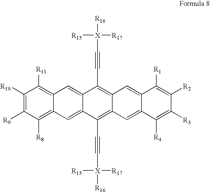


Compound Group 9 is Represented by Formula 9:


wherein each R′ is independently selected from a C2-40 alkyl group, a C2-40 alkoxy group, a C2-40 alkenyl group, C2-40 alkynyl group, a C6-18 aryl or heteroaryl group, C6-C40 aryloxy group, C7-C40 alkylaryloxy group, a C2-C40 alkoxycarbonyl group, a C7-C40 aryloxycarbonyl group, or a silyl group, each of which may be optionally substituted, or a cyano group (—CN), a carbamoyl group (—C(═O)NH2), a haloformyl group (—C(═O)—X, wherein X represents a halogen atom), a formyl group (—C(═O)—H), an isocyano group, an isocyanate group, a thiocyanate group or a thioisocyanate group, an optionally substituted amino group, an imino group, a hydroxy group, a halo, a sulpho group, a sulphonyl group a mercapto group, or a nitro group; and m and n in Formula 8B are each independently 0, 1, 2, 3 or 4, more preferably 0, 1 or 2. Preferably, in Formulae 1A, 8A and 8B each R′ is independently selected from C6-18 aryl and silyl, which may both optionally be substituted. Preferably in Formula 1A, 8A and 8B at least one R′ and most preferably both R′ is silyl, wherein the silyl group is preferably defined as above, that is, a silyl group of formula —Si(R15)(R16)(R17). These latter highly preferred compounds thus have Formulae 1A′, 8A′ and 8B′:


| TABLE 1 | ||
| Hansen parameter | ||
| δd MPa1/2 | δp MPa1/2 | δh MPa1/2 | ||
| Preferred range | 14.5+ | 0-10 | 0-14 | ||
| More preferred range | 16+ | 0-9 | 0-12 | ||
| Most preferred range | 17+ | 0-8 | 0-10 | ||
| TABLE 2 | |||
| typical low frequency | |||
| Binder | permittivity ε | ||
| Polystyrene | 2.5 | ||
| poly(α-methylstyrene) | 2.6 | ||
| poly(α-vinylnaphtalene) | 2.6 | ||
| poly(vinyltoluene) | 2.6 | ||
| Polyethylene | 2.2-2.3 | ||
| cis-polybutadiene | 2.0 | ||
| Polypropylene | 2.2 | ||
| Polyisoprene | 2.3 | ||
| poly(4-methyl-1-pentene) | 2.1 | ||
| poly(4-methylstyrene) | 2.7 | ||
| poly(chorotrifluoroethylene) | 2.3-2.8 | ||
| poly(2-methyl-1,3-butadiene) | 2.4 | ||
| poly(p-xylylene) | 2.6 | ||
| poly(α-α-α′-α′ tetrafluoro-p-xylylene) | 2.4 | ||
| poly[1,1-(2-methyl | 2.3 | ||
| propane)bis(4-phenyl)carbonate] | |||
| poly(cyclohexyl methacrylate) | 2.5 | ||
| poly(chlorostyrene) | 2.6 | ||
| poly(2,6-dimethyl-1,4-phenylene ether) | 2.6 | ||
| Polyisobutylene | 2.2 | ||
| poly(vinyl cyclohexane) | 2.2 | ||
| poly(vinylcinnamate) | 2.9 | ||
| poly(4-vinylbiphenyl) | 2.7 | ||
| TABLE 3 | |
| typical low frequency | |
| Binder | permittivity (ε) |
| Poly(ethylene/tetrafluoroethylene) | 2.6 |
| poly(ethylene/chlorotrifluoroethylene) | 2.3 |
| fluorinated ethylene/propylene copolymer | 2-2.5 |
| polystyrene-co-α-methylstyrene | 2.5-2.6 |
| ethylene/ethyl acrylate copolymer | 2.8 |
| poly(styrene/10% butadiene) | 2.6 |
| poly(styrene/15% butadiene) | 2.6 |
| poly(styrene/2,4 dimethylstyrene) | 2.5 |
| Topas ™ (all grades), | 2.2-2.3 |
| cyclic olefin copolymer | |
A(c)B(d) . . . X(z) Formula 11


in which X may be Se, Te, O, S or —N(Rc) more preferably X is O, S or —N(Rc)—, wherein Rc represents H, optionally substituted alkyl or optionally substituted aryl; and R1 and R2 are as previously described in relation to Formula 12;

in which R1, R2 and X are as previously described in relation to Formulae 12 and 13 respectively;

in which R1, R2 and X are as previously described in relation to Formulae 12 and 13 respectively; and Z represents —C(T1)=C(T2)-, —C≡C—, —N(R′)—, —N═N—, (R′)═N—, —N═C(R′)—, wherein T1 and T2 independently represent —H, Cl, F, —C≡N or a lower alkyl and R′ represents —H, alkyl, substituted alkyl, aryl, or substituted aryl;

wherein R1 and R2 are as previously described in relation to Formulae 12;

wherein R1 to R4 may be independently selected from the same list of groups as described for R1 and R2 in
-
- (i) first mixing both a polyacene compound and an organic binder, preferably the mixing comprises mixing the two components together in a solvent or solvent mixture. The solvent may be a single solvent or the polyacene compound and the organic binder may each be dissolved in a separate solvent followed by mixing the two resultant solutions to mix the compounds; and
- (ii) applying the solvent(s) containing the polyacene compound and the organic binder to a substrate; and
- (iii) optionally evaporating the solvent(s) to form the layer of the invention.
wherein:
a=mass of polyacene, b=mass of binder and c=mass of solvent.


where V0 is an offset voltage and IΩ is an ohmic current independent of the gate voltage and is due to the finite conductivity of the material. The other parameters have been described above.
| TABLE 4 |
| OFET performance of semiconductor formulations prepared with and without binder material |
| OSC and binder | ||||||
| Organic | solids content in | OSC:Binder | ||||
| Example | Semiconducting | coating solution | Ratio | Mobility [cm2/Vs] | Sample | |
| number | Material (OSC) | (by weight) | Binder | (wt:wt) | (+/−1 std. dev.) | |
| 12 | |
1% | p-αMS | 50:50 | 0.433 | (+/−0.19) | 9 |
| (example 1) | |||||||
| 13 | |
1% | — | 100:0 | 0.14 | (+/−0.14) | 6 |
| (comparative) | |||||||
| 14 | |
1% | p-αMS | 50:50 | 1.1 | (+/−0.4) | 15 |
| (example 3) | |||||||
| 15 | |
1% | — | 100:0 | 0.11 | (+/−0.14) | 7 |
| (comparative) | |||||||
| TABLE 5 |
| Mobility measurements for OFETs prepared using a range of polymeric binders |
| OSC & binder | |||||||
| Organic | Binder mixed at | solids content in | Permittivity | ||||
| Example | semiconducting | 1:1 (by weight) | coating solution | Mobility [cm2/Vs] | Sample | of binder ε | |
| number | material (OSC) | with polyacene | (by weight) | Solvent | (+/−1 std. dev.) | size | 1 kHz |
| 12 | Compound 1 | p-αMS | 1% | toluene | 0.433 | (+/−0.19) | 9 | 2.6a |
| 14 | Compound 4 | p-αMS | 1% | 1,2-Dichlorobenzene | 1.1 | (+/−0.4) | 15 | 2.6a |
| 16 | Compound 1 | Topas 8007 | 4% | Ethylcyclohexane | 0.26 | (+/−0.090) | 7 | 2.2-2.3b |
| 17 | Compound 1 | Topas 8007 | 4% | Anisole | 0.26 | (+/−0.082) | 5 | 2.2-2.3b |
| 18 | Compound 1 | PS (1M) | 4% | p-xylene | 0.20 | (+/−0.085) | 8 | 2.5a |
| 19 | Compound 1 | p-4-MS | 4% | p-xylene | 0.26 | (+/−0.11) | 5 | 2.7c |
| 20 | Compound 1 | PS-co-αMS | 4% | p-xylene | 0.21 | (+/−0.19) | 5 | 2.5-2.6a |
| 21 | Compound 4 | poly(vinyl- | 1% | 1,2-Dichlorobenzene | 1.4 ± 0.47 | 8 | 2.9c |
| cinnamate) |
| 22 | Compound 1 | PMMA | 4% | Acetone | 0.0029 | (+/−0.0025) | 6 | 3.5d |
| (comparative) |
| 23 | Compound 1 | PVP | 1% | Acetone | No FET mobility | 4.5e | |
| (comparative) | was observed | ||||||
| 24 | Compound 1 | PVA | 1% | Acetone | No FET mobility | 10.4a | |
| (comparative) | was observed | ||||||
| 25 | Compound 4 | poly(4- | 1% | 1,2-Dichlorobenzene | 1.0 ± 0.66 | 8 | 2.7c |
| vinylbiphenyl) |
| 26 | Isomeric mixture | p-αMS | 1% | toluene | 0.16 | (+/−0.025) | 4 | 2.6a |
| of Compounds 19 | ||||||||
| and 20 | ||||||||
Topas™ 8007—ex. Ticona (linear olefin and cycloolefin(norbornene)copolymer), (examples 16 and 17);
PS (1M)—polystyrene Mw=1,000,000 Aldrich catalogue number 48,080-0, (example 18);
p-4-MS—poly-4-methylstyrene Aldrich catalogue number 18,227-3, (example 19)
PS-co-αMS—Polystyrene-co-alpha-methyl styrene Aldrich catalogue number 45,721-3, (example 20);
poly(vinylcinnamate) Aldrich No:18,264-8, (example 21)
PMMA—polymethylmethacrylate Mn=797, (example 22)
PVP—poly-4-vinylphenol Aldrich catalogue number 43,622-4, (comparative example 23);
PVA—polyvinylalcohol Aldrich catalogue number 36,316-2, (comparative example 24);
poly(4-vinylbiphenyl) Aldrich catalogue number 18,254-0, (example 25);
a Polymer Handbook (3rd edition) Wiley and Sons (1989).
b manufacturer's data
c Obtained by measuring the capacitance and thickness of a film of binder between two metal electrodes and then calculating the dielectric constant ∈ using the relationship
∈=Cd/E 0 A
where C is capacitance, d is the film thickness, E0 is the permittivity of free space, and A is the area of the capacitor.
d Ficker et al., J. Appl. Phys. 2003 94 (4), 2638.
e Stutzman et al. Science 2003, 299, 1881.
| TABLE 6 |
| Mobility measurements for OFETs prepared using a semiconducting binder |
| OSC and binder | Permittivity of | ||||||
| Organic semi- | Binder mixed at | solids content in | semiconducting | ||||
| Example | conducting | 1:1 (by weight) | coating solution | Mobility [cm2/Vs] | Sample | binder ε at 1 | |
| number | material (OSC) | with polyacene | (by weight) | Solvent | (+/−1 std. dev.) | size | kHz |
| 27 | | poly(9-vinylcarbazol) | 1% | 1,2-Dichlorobenzene | 1.44 ± 0.35 | 7 | 2.7* |
| 28 | | | 4% | p-xylene | 0.28 (+/−0.09) | 7 | 2.9c |
In Table 6, the poly(9-vinylcarbazol) is available from Aldrich, catalogue number: 18,260-5 (example 27).
•—refers to Schaffert R. M. IBM Journal of Res. And Devel. Vol 15 No1, p79 (1971)
c—has the same meanings as in Table 5.
PTAA1—is a triarylamine compound of Formula 18.

wherein n=10.7 and Mn=3100 (Adv. Funct. Mater. 2003, 13, No. 3. p199-204)
| TABLE 7 |
| Mobility measurements for OFETs prepared with varying quantities of binder to OSC material |
| OSC and binder | ||||||
| Organic | solids content in | OSC:Binder | ||||
| Example | Semiconducting | coating solution | Ratio | Sample | ||
| number | Material (OSC) | Binder | (by weight) | (wt:wt) | Mobility [cm2/Vs] | |
| 12 | Compound 1 | p- | 1% | 50:50 | 0.433 (+/−0.19) | 9 |
| 29 | Compound 1 | p- | 1% | 75:25 | 0.321 (+/−0.11) | 7 |
| 30 | Compound 1 | p- | 1% | 90:10 | 0.327 (+/−0.11) | 6 |
| 31 | Compound 1 | p- | 1% | 95:5 | 0.244 (+/−0.077) | 8 |
The above results illustrate that excellent mobility values can be obtained for an OFET device even when the ratio of OSC material to binder is 50:50.
| TABLE 8 |
| Variation of the solids content in a coating solution used to prepare an OFET |
| OSC and binder | |||||
| Organic | Binder mixed at | solids content in | |||
| Example | semiconducting | 1:1 (by weight) | coating solution | Mobility [cm2/Vs] | Sample |
| number | material (OSC) | with polyacene | (by weight) | (+/−1 std. dev.) | size |
| 32 | Compound 1 | p-αMS | 0.5% | 0.29 (+/−0.23) | 9 |
| 33 | Compound 1 | p- |
1% | 0.40 (+/−0.14) | 11 |
| 34 | Compound 1 | p- |
2% | 0.39 (+/−0.15) | 11 |
| 35 | Compound 1 | p- |
4% | 0.53 (+/−0.07) | 11 |
Claims (39)


Priority Applications (3)
| Application Number | Priority Date | Filing Date | Title |
|---|---|---|---|
| US11/671,877 US7807993B2 (en) | 2003-11-28 | 2007-02-06 | Organic pentacene semiconducting layers |
| US11/822,594 US7576208B2 (en) | 2003-11-28 | 2007-07-09 | Organic semiconductor layers |
| US12/719,545 US8119804B2 (en) | 2003-11-28 | 2010-03-08 | Organic semiconducting layers |
Applications Claiming Priority (7)
| Application Number | Priority Date | Filing Date | Title |
|---|---|---|---|
| GB0327654A GB0327654D0 (en) | 2003-11-28 | 2003-11-28 | Improvements in and relating to organic semiconducting layers |
| GB0327654.0 | 2003-11-28 | ||
| GB0407852A GB0407852D0 (en) | 2004-04-07 | 2004-04-07 | Improvements in and relating to organic semi-conducting layers |
| GB0407852.3 | 2004-04-07 | ||
| GB0414347.5 | 2004-06-26 | ||
| GB0414347A GB0414347D0 (en) | 2004-06-26 | 2004-06-26 | Improvements in and relating to organic semiconducting layers |
| PCT/GB2004/004973 WO2005055248A2 (en) | 2003-11-28 | 2004-11-25 | Organic semiconducting layer formulations comprising polyacenes and organic binder polymers |
Related Parent Applications (1)
| Application Number | Title | Priority Date | Filing Date |
|---|---|---|---|
| PCT/GB2004/004973 A-371-Of-International WO2005055248A2 (en) | 2003-11-28 | 2004-11-25 | Organic semiconducting layer formulations comprising polyacenes and organic binder polymers |
Related Child Applications (1)
| Application Number | Title | Priority Date | Filing Date |
|---|---|---|---|
| US11/671,877 Division US7807993B2 (en) | 2003-11-28 | 2007-02-06 | Organic pentacene semiconducting layers |
Publications (2)
| Publication Number | Publication Date |
|---|---|
| US20070102696A1 US20070102696A1 (en) | 2007-05-10 |
| US7842942B2 true US7842942B2 (en) | 2010-11-30 |
Family
ID=34657583
Family Applications (4)
| Application Number | Title | Priority Date | Filing Date |
|---|---|---|---|
| US10/580,552 Active 2025-06-02 US7842942B2 (en) | 2003-11-28 | 2004-11-25 | Organic semiconducting layers |
| US11/671,877 Active 2025-07-15 US7807993B2 (en) | 2003-11-28 | 2007-02-06 | Organic pentacene semiconducting layers |
| US11/822,594 Active US7576208B2 (en) | 2003-11-28 | 2007-07-09 | Organic semiconductor layers |
| US12/719,545 Active 2026-06-18 US8119804B2 (en) | 2003-11-28 | 2010-03-08 | Organic semiconducting layers |
Family Applications After (3)
| Application Number | Title | Priority Date | Filing Date |
|---|---|---|---|
| US11/671,877 Active 2025-07-15 US7807993B2 (en) | 2003-11-28 | 2007-02-06 | Organic pentacene semiconducting layers |
| US11/822,594 Active US7576208B2 (en) | 2003-11-28 | 2007-07-09 | Organic semiconductor layers |
| US12/719,545 Active 2026-06-18 US8119804B2 (en) | 2003-11-28 | 2010-03-08 | Organic semiconducting layers |
Country Status (8)
| Country | Link |
|---|---|
| US (4) | US7842942B2 (en) |
| EP (3) | EP1687830B1 (en) |
| JP (2) | JP5089986B2 (en) |
| KR (1) | KR101217963B1 (en) |
| AT (1) | ATE475971T1 (en) |
| DE (1) | DE602004028399D1 (en) |
| TW (1) | TWI358144B (en) |
| WO (1) | WO2005055248A2 (en) |
Cited By (6)
| Publication number | Priority date | Publication date | Assignee | Title |
|---|---|---|---|---|
| US20110180787A1 (en) * | 2008-07-03 | 2011-07-28 | Postech Academy-Industry Foundation | Ink-Jet Print Ink and Organic Thin Film Transister Using Thereof |
| US20120061620A1 (en) * | 2009-05-29 | 2012-03-15 | Robert Steven Clough | Fluorinated Silyethynyl Pentacene Compounds and Compositions and Methods of Making and Using the Same |
| US20120161108A1 (en) * | 2010-12-23 | 2012-06-28 | Xerox Corporation | Tetrahydrotetraazapentacenes in thin-film transistors |
| US9954173B2 (en) | 2012-08-09 | 2018-04-24 | Merck Patent Gmbh | Organic semiconducting formulation |
| US10005796B2 (en) | 2014-05-01 | 2018-06-26 | University Of Massachusetts | Substituted angular bistetracenes and substituted angular bisoligoacenes and electronic devices made with same |
| US10121970B2 (en) * | 2011-05-26 | 2018-11-06 | Wuhan Xinqu Chuangrou Optoelectronics Technology Co., Ltd. | Transistors and methods for making them |
Families Citing this family (230)
| Publication number | Priority date | Publication date | Assignee | Title |
|---|---|---|---|---|
| KR100682860B1 (en) * | 2004-01-27 | 2007-02-15 | 삼성에스디아이 주식회사 | Spirofluorene-based polymer and organo-electroluminescent device using the same |
| KR100857670B1 (en) * | 2004-06-01 | 2008-09-08 | 도쿠리쓰교세이호징 가가쿠 기주쓰 신코 기코 | Photoelectric conversion devices |
| US7385221B1 (en) * | 2005-03-08 | 2008-06-10 | University Of Kentucky Research Foundation | Silylethynylated heteroacenes and electronic devices made therewith |
| US20060220007A1 (en) * | 2005-04-05 | 2006-10-05 | Bailey David B | Acene compounds having a single terminal fused thiophene as semiconductor materials for thin film transistors and methods of making the same |
| EP1986247A1 (en) | 2005-05-12 | 2008-10-29 | MERCK PATENT GmbH | Polyacene and semiconductor Formulation |
| JP2008545631A (en) * | 2005-05-21 | 2008-12-18 | メルク パテント ゲゼルシャフト ミット ベシュレンクテル ハフトング | Oligomer polyacene and semiconductor preparations |
| US20090107539A1 (en) * | 2005-08-02 | 2009-04-30 | Adeka Corporation | Photoelectric device |
| JP5034196B2 (en) * | 2005-09-16 | 2012-09-26 | コニカミノルタホールディングス株式会社 | Organic semiconductor material, organic semiconductor film, organic semiconductor device, and organic thin film transistor |
| JP5223337B2 (en) * | 2005-12-06 | 2013-06-26 | コニカミノルタホールディングス株式会社 | Organic semiconductor material, organic semiconductor film, organic semiconductor device, and organic thin film transistor |
| CN101356662B (en) * | 2005-12-12 | 2014-08-06 | 西巴控股有限公司 | Organic semiconductors and semiconductor device comprising the same |
| US20070146426A1 (en) * | 2005-12-28 | 2007-06-28 | Nelson Brian K | All-inkjet printed thin film transistor |
| US7514710B2 (en) | 2005-12-28 | 2009-04-07 | 3M Innovative Properties Company | Bottom gate thin film transistors |
| US20100308304A1 (en) * | 2006-01-21 | 2010-12-09 | Simon Dominic Ogier | Electronic short channel device comprising an organic semiconductor formulation |
| US7667230B2 (en) | 2006-03-31 | 2010-02-23 | 3M Innovative Properties Company | Electronic devices containing acene-thiophene copolymers |
| US7608679B2 (en) | 2006-03-31 | 2009-10-27 | 3M Innovative Properties Company | Acene-thiophene copolymers |
| US7586120B2 (en) * | 2006-04-06 | 2009-09-08 | Xerox Corporation | Ethynylene acene polymers and electronic devices generated therefrom |
| US8334391B2 (en) * | 2006-04-06 | 2012-12-18 | Xerox Corporation | Functionalized heteroacenes |
| US7372071B2 (en) * | 2006-04-06 | 2008-05-13 | Xerox Corporation | Functionalized heteroacenes and electronic devices generated therefrom |
| US7557370B2 (en) * | 2006-04-06 | 2009-07-07 | Xerox Corporation | Heteroacene polymers and electronic devices generated therefrom |
| US7495251B2 (en) * | 2006-04-21 | 2009-02-24 | 3M Innovative Properties Company | Electronic devices containing acene-thiophene copolymers with silylethynyl groups |
| US7666968B2 (en) | 2006-04-21 | 2010-02-23 | 3M Innovative Properties Company | Acene-thiophene copolymers with silethynly groups |
| JP2007294718A (en) * | 2006-04-26 | 2007-11-08 | Konica Minolta Holdings Inc | Organic semiconductor film and organic thin-film transistor |
| CN101495535B (en) | 2006-07-21 | 2012-06-20 | 默克专利有限公司 | Copolymers of indenofluorene and thiophene |
| KR20090077779A (en) * | 2006-10-12 | 2009-07-15 | 이데미쓰 고산 가부시키가이샤 | Organic thin film transistor device and organic thin film light-emitting transistor |
| WO2008063583A1 (en) * | 2006-11-17 | 2008-05-29 | Polyera Corporation | Acene-based organic semiconductor materials and methods of preparing and using the same |
| US7902086B2 (en) * | 2006-12-08 | 2011-03-08 | Spansion Llc | Prevention of oxidation of carrier ions to improve memory retention properties of polymer memory cell |
| KR101314998B1 (en) * | 2006-12-13 | 2013-10-04 | 삼성전자주식회사 | Heteroacenes, organic thin film comprising the compounds and electronic device comprising the thin film |
| GB2460579B (en) * | 2007-03-07 | 2011-11-02 | Univ Kentucky Res Found | Silylethynylated heteroacenes and electronic devices made therewith |
| CN101663309B (en) | 2007-04-19 | 2013-08-14 | 默克专利股份有限公司 | Process for preparing substituted pentacenes |
| JP2008291236A (en) * | 2007-04-25 | 2008-12-04 | Hitachi Ltd | Organic light-emitting display device |
| CN101668763A (en) * | 2007-04-28 | 2010-03-10 | 默克专利股份有限公司 | organic semiconductors |
| US7879688B2 (en) | 2007-06-29 | 2011-02-01 | 3M Innovative Properties Company | Methods for making electronic devices with a solution deposited gate dielectric |
| US20090001356A1 (en) * | 2007-06-29 | 2009-01-01 | 3M Innovative Properties Company | Electronic devices having a solution deposited gate dielectric |
| WO2009016107A1 (en) * | 2007-07-30 | 2009-02-05 | Basf Se | Method for depositing a semiconducting layer from a liquid |
| EP2232606A1 (en) * | 2007-12-17 | 2010-09-29 | 3M Innovative Properties Company | Solution processable organic semiconductors based on anthracene |
| KR101932806B1 (en) | 2008-03-06 | 2018-12-27 | 메르크 파텐트 게엠베하 | Organic semiconductor formulation |
| JP2009227838A (en) * | 2008-03-24 | 2009-10-08 | Fujifilm Corp | Composition for film formation, insulating film and electronic device |
| JP5480510B2 (en) | 2008-03-31 | 2014-04-23 | 住友化学株式会社 | Organic semiconductor composition, organic thin film, and organic thin film element comprising the same |
| WO2009129912A1 (en) | 2008-04-24 | 2009-10-29 | Merck Patent Gmbh | Electronic device |
| KR101622420B1 (en) * | 2008-05-30 | 2016-05-18 | 쓰리엠 이노베이티브 프로퍼티즈 컴파니 | Silylethynyl pentacene compounds and compositions and methods of making and using the same |
| US8232550B2 (en) | 2008-06-11 | 2012-07-31 | 3M Innovative Properties Company | Mixed solvent systems for deposition of organic semiconductors |
| CN102119164A (en) * | 2008-06-19 | 2011-07-06 | 3M创新有限公司 | Solution processable organic semiconductors |
| JP4730623B2 (en) * | 2008-07-24 | 2011-07-20 | ソニー株式会社 | THIN FILM TRANSISTOR, METHOD FOR PRODUCING THIN FILM TRANSISTOR, AND ELECTRONIC DEVICE |
| JP4552160B2 (en) * | 2008-07-30 | 2010-09-29 | ソニー株式会社 | Method for forming organic semiconductor thin film and method for manufacturing thin film semiconductor device |
| KR101000784B1 (en) | 2008-07-30 | 2010-12-13 | 한국화학연구원 | Novel polyacene compounds substituted with dendron and organic thin film transistor using the same |
| US20110136282A1 (en) * | 2008-08-05 | 2011-06-09 | Toray Industries, Inc. | Method for producing device |
| US20100032654A1 (en) * | 2008-08-11 | 2010-02-11 | Motorola, Inc. | Semiconductor Device Having Silane Treated Interface |
| EP2315793B1 (en) | 2008-08-18 | 2013-08-21 | Merck Patent GmbH | Indacenodithiophene and indacenodiselenophene polymers and their use as organic semiconductors |
| US8709290B2 (en) | 2008-09-19 | 2014-04-29 | Merck Patent Gesellschaft Mit Beschrankter Haftung | Polymers derived from benzobis(silolothiophene) and their use as organic semiconductors |
| DE112009001782T5 (en) | 2008-09-19 | 2011-07-28 | Merck Patent GmbH, 64293 | Bis (thienocyclopenta) benzothiadiazole-derived polymers and their use as organic semiconductors |
| JP5498674B2 (en) * | 2008-09-19 | 2014-05-21 | 出光興産株式会社 | Organic thin film solar cell material and organic thin film solar cell using the same |
| JP5529416B2 (en) * | 2009-01-22 | 2014-06-25 | 旭化成株式会社 | Organic semiconductor thin film and organic semiconductor element |
| WO2010099583A1 (en) * | 2009-03-05 | 2010-09-10 | Commonwealth Scientific And Industrial Research Organisation | Photosensitive optoelectronic devices comprising polycyclic aromatic compounds |
| CN102421858A (en) | 2009-06-22 | 2012-04-18 | 默克专利有限公司 | Conducting formulation |
| JP5778148B2 (en) | 2009-08-04 | 2015-09-16 | メルク パテント ゲーエムベーハー | Electronic devices containing polycyclic carbohydrates |
| GB2485127A (en) | 2009-08-12 | 2012-05-02 | Merck Patent Gmbh | Phenanthro [1,10,9,8-C,D,E,F,G] carbazole polymers and their use as organic semiconductors |
| WO2011026550A1 (en) | 2009-09-05 | 2011-03-10 | Merck Patent Gmbh | Solution processable passivation layers for organic electronic devices |
| US7948016B1 (en) | 2009-11-03 | 2011-05-24 | 3M Innovative Properties Company | Off-center deposition of organic semiconductor in an organic semiconductor device |
| US8822731B2 (en) * | 2009-11-30 | 2014-09-02 | University Of New Hampshire | Soluble, persistent nonacene derivatives |
| US8513466B2 (en) * | 2009-11-30 | 2013-08-20 | University Of New Hampshire | Class of soluble, photooxidatively resistant acene derivatives |
| CN102695741B (en) * | 2009-12-11 | 2015-07-08 | 普罗米鲁斯有限责任公司 | Norbornene-type polymers having quaternary ammonium functionality |
| US8765894B2 (en) * | 2009-12-11 | 2014-07-01 | Promerus, Llc | Norbornene-type polymers having quaternary ammonium functionality |
| KR20170093267A (en) * | 2009-12-23 | 2017-08-14 | 메르크 파텐트 게엠베하 | Compositions comprising organic semiconducting compounds |
| US9178156B2 (en) * | 2009-12-23 | 2015-11-03 | Merck Patent Gmbh | Compositions comprising polymeric binders |
| US8212243B2 (en) | 2010-01-22 | 2012-07-03 | Eastman Kodak Company | Organic semiconducting compositions and N-type semiconductor devices |
| US20110180785A1 (en) * | 2010-01-27 | 2011-07-28 | Christoph Wilhelm Sele | Transistor structure comprising a chemical additive, a display and an electronic apparatus |
| RU2012139316A (en) | 2010-02-15 | 2014-03-27 | Мерк Патент Гмбх | SEMICONDUCTOR POLYMERS |
| EP2539949B1 (en) | 2010-02-25 | 2018-01-10 | Merck Patent GmbH | Electrode treatment process for organic electronic devices |
| WO2011116866A1 (en) | 2010-03-24 | 2011-09-29 | Merck Patent Gmbh | Polymers of 8,9-dihydrobenzo[def]carbazole and their use as organic semiconductors |
| JP2013527980A (en) | 2010-04-12 | 2013-07-04 | メルク パテント ゲーエムベーハー | Composition with improved performance |
| US20130026421A1 (en) | 2010-04-12 | 2013-01-31 | Merck Patent Gmbh | Composition and method for preparation of organic electronic devices |
| US10050201B2 (en) | 2010-04-19 | 2018-08-14 | Merck Patent Gmbh | Polymers of benzodithiophene and their use as organic semiconductors |
| EP2381503B1 (en) | 2010-04-23 | 2013-04-17 | Polyphotonix Limited | Method for manufacturing material for use in manufacturing electroluminescent organic semiconductor devices |
| WO2011147522A1 (en) | 2010-05-27 | 2011-12-01 | Merck Patent Gmbh | Compositions comprising quantum dots |
| RU2012156386A (en) | 2010-05-27 | 2014-07-10 | Мерк Патент Гмбх | COMPOSITION AND METHOD FOR PRODUCING ORGANIC ELECTRONIC DEVICES |
| US8779179B2 (en) | 2010-05-28 | 2014-07-15 | 3M Innovative Properties Company | Synthesis of silyl acetylenes |
| WO2011150020A1 (en) | 2010-05-28 | 2011-12-01 | 3M Innovative Properties Company | Synthesis of silyl acetylenes |
| JP2013534726A (en) | 2010-06-24 | 2013-09-05 | メルク パテント ゲゼルシャフト ミット ベシュレンクテル ハフツング | Method for modifying electrodes in organic electronic devices |
| WO2012003919A2 (en) | 2010-07-08 | 2012-01-12 | Merck Patent Gmbh | Semiconducting polymers |
| DE112011102301T5 (en) | 2010-07-09 | 2013-05-16 | Merck Patent Gmbh | Semiconducting polymers |
| WO2012013272A1 (en) | 2010-07-26 | 2012-02-02 | Merck Patent Gmbh | Quantum dots and hosts |
| EP2599142A1 (en) | 2010-07-26 | 2013-06-05 | Merck Patent GmbH | Nanocrystals in devices |
| RU2013110785A (en) | 2010-08-13 | 2014-09-20 | Мерк Патент Гмбх | ANTRA DERIVATIVES [2,3-b: 7,6-b '] DITHIOPHENE AND THEIR APPLICATION AS ORGANIC SEMICONDUCTORS |
| GB201013820D0 (en) | 2010-08-18 | 2010-09-29 | Cambridge Display Tech Ltd | Low contact resistance organic thin film transistors |
| RU2013114414A (en) | 2010-09-02 | 2014-10-10 | Мерк Патент Гмбх | DIELECTRIC SHUTTER LAYER FOR ELECTRONIC DEVICES |
| DE112011102916T5 (en) | 2010-09-02 | 2013-06-27 | Merck Patent Gmbh | Interlayer for electronic devices |
| KR20130112882A (en) | 2010-09-02 | 2013-10-14 | 메르크 파텐트 게엠베하 | Process for preparing an organic electronic device |
| WO2012028246A1 (en) | 2010-09-04 | 2012-03-08 | Merck Patent Gmbh | Conjugated polymers |
| SG188395A1 (en) | 2010-09-10 | 2013-04-30 | Merck Patent Gmbh | Anthra[2,3-b:7,6b']dithiophene derivatives and their use as organic semiconductors |
| DE102010046412B4 (en) | 2010-09-23 | 2022-01-13 | Merck Patent Gmbh | metal-ligand coordination compounds |
| CN103168063B (en) | 2010-10-20 | 2016-11-23 | 默克专利股份有限公司 | Conjugated polymer |
| RU2013130877A (en) * | 2010-12-06 | 2015-01-20 | Мерк Патент Гмбх | NONLINEAR ACENE DERIVATIVES AND THEIR APPLICATION AS ORGANIC SEMICONDUCTORS |
| DE102010054525A1 (en) | 2010-12-15 | 2012-04-26 | Merck Patent Gmbh | Organic electroluminescent device |
| CN103261204B (en) | 2010-12-17 | 2016-08-10 | 默克专利股份有限公司 | Conjugated polymer |
| DE102010055902A1 (en) | 2010-12-23 | 2012-06-28 | Merck Patent Gmbh | Organic electroluminescent device |
| US8643001B2 (en) * | 2010-12-23 | 2014-02-04 | Samsung Electronics Co. Ltd. | Semiconductor composition |
| DE102010055901A1 (en) | 2010-12-23 | 2012-06-28 | Merck Patent Gmbh | Organic electroluminescent device |
| US9373801B2 (en) | 2011-01-28 | 2016-06-21 | Merck Patent Gmbh | Flavanthrene derivatives and their use as organic semiconductors |
| EP2675524B1 (en) | 2011-02-14 | 2017-05-10 | Merck Patent GmbH | Device and method for treatment of cells and cell tissue |
| US8742403B2 (en) * | 2011-03-08 | 2014-06-03 | Samsung Electronics Co., Ltd. | Xanthene based semiconductor compositions |
| EP2683726A1 (en) | 2011-03-11 | 2014-01-15 | Merck Patent GmbH | Dinaphtho[2,3-a:2',3'-h]phenazines and their use as organic semiconductors |
| WO2012123060A1 (en) | 2011-03-11 | 2012-09-20 | Merck Patent Gmbh | Conjugated polymers |
| EP2503616A1 (en) | 2011-03-21 | 2012-09-26 | Polyphotonix Limited | Emissive element for light emitting device, light emitting device and method for manufacturing such element and device |
| JP6356060B2 (en) | 2011-03-24 | 2018-07-11 | メルク パテント ゲーエムベーハー | Organic ionic functional materials |
| KR20140031876A (en) | 2011-03-25 | 2014-03-13 | 메르크 파텐트 게엠베하 | Pyrrolo[3,2-b]pyrrole-2,5-diones and their use as organic semiconductors |
| CN103477462B (en) * | 2011-04-05 | 2016-05-25 | 默克专利有限公司 | Organic electroluminescence device |
| KR20140037085A (en) | 2011-04-18 | 2014-03-26 | 메르크 파텐트 게엠베하 | Conjugated polymers |
| WO2012152366A1 (en) | 2011-05-12 | 2012-11-15 | Merck Patent Gmbh | Organic ionic compounds, compositions and electronic devices |
| WO2012156022A1 (en) | 2011-05-16 | 2012-11-22 | Merck Patent Gmbh | Conjugated polymers |
| GB201108865D0 (en) | 2011-05-26 | 2011-07-06 | Ct For Process Innovation The Ltd | Semiconductor compounds |
| GB2491810B (en) | 2011-05-31 | 2018-03-21 | Smartkem Ltd | Organic semiconductor compositions |
| JP2014517524A (en) | 2011-06-01 | 2014-07-17 | メルク パテント ゲゼルシャフト ミット ベシュレンクテル ハフツング | Hybrid bipolar TFT |
| US8963131B2 (en) * | 2011-06-13 | 2015-02-24 | Samsung Electronics Co., Ltd. | Electronic device |
| DE102011104745A1 (en) | 2011-06-17 | 2012-12-20 | Merck Patent Gmbh | Materials for organic electroluminescent devices |
| JP6301830B2 (en) | 2011-06-28 | 2018-03-28 | メルク パテント ゲゼルシャフト ミット ベシュレンクテル ハフツングMerck Patent Gesellschaft mit beschraenkter Haftung | Indaceno derivatives as organic semiconductors |
| CN103649163A (en) | 2011-07-08 | 2014-03-19 | 默克专利股份有限公司 | Conjugated polymers |
| KR101935077B1 (en) | 2011-07-19 | 2019-01-03 | 메르크 파텐트 게엠베하 | Organic semiconductors |
| JP6101264B2 (en) | 2011-07-21 | 2017-03-22 | メルク パテント ゲゼルシャフト ミット ベシュレンクテル ハフツングMerck Patent Gesellschaft mit beschraenkter Haftung | Conjugated polymer |
| JP6174024B2 (en) | 2011-07-25 | 2017-08-02 | メルク パテント ゲーエムベーハー | Copolymers with functional side chains |
| WO2013013753A2 (en) | 2011-07-25 | 2013-01-31 | Merck Patent Gmbh | Polymers and oligomers with functionalized side groups |
| US20140319428A1 (en) | 2011-07-27 | 2014-10-30 | Merck Patent Gmbh | Small molecules and their use as organic semiconductors |
| GB201116251D0 (en) | 2011-09-20 | 2011-11-02 | Cambridge Display Tech Ltd | Organic semiconductor composition and organic transistor |
| EP2760909B1 (en) | 2011-09-28 | 2017-03-01 | Merck Patent GmbH | Conjugated polymers |
| WO2013052153A1 (en) | 2011-10-05 | 2013-04-11 | Georgia Tech Research Corporation | Blends of organic semiconductor compounds and electrically insulating amorphous polymers, methods and devices |
| US20140252279A1 (en) | 2011-10-20 | 2014-09-11 | Merck Patent Gmbh | Organic semiconductors |
| GB201118997D0 (en) | 2011-11-03 | 2011-12-14 | Cambridge Display Tech Ltd | Electronic device and method |
| EP2789025B1 (en) | 2011-12-07 | 2015-09-30 | Basf Se | An organic field effect transistor |
| CN104136484B (en) | 2012-02-15 | 2017-02-22 | 默克专利股份有限公司 | Conjugated polymers |
| EP2814862A2 (en) | 2012-02-15 | 2014-12-24 | Merck Patent GmbH | Conjugated polymers |
| WO2013120581A1 (en) | 2012-02-15 | 2013-08-22 | Merck Patent Gmbh | Planarization layer for organic electronic devices |
| GB2514508A (en) | 2012-02-16 | 2014-11-26 | Merck Patent Gmbh | Organic semiconducting polymers |
| GB201203159D0 (en) * | 2012-02-23 | 2012-04-11 | Smartkem Ltd | Organic semiconductor compositions |
| TWI635111B (en) | 2012-03-16 | 2018-09-11 | 馬克專利公司 | Conjugated polymers |
| WO2013159862A1 (en) | 2012-04-25 | 2013-10-31 | Merck Patent Gmbh | Conjugated polymers |
| CN104245787B (en) | 2012-04-25 | 2017-02-22 | 默克专利股份有限公司 | Conjugated polymers |
| WO2013159881A2 (en) | 2012-04-25 | 2013-10-31 | Merck Patent Gmbh | Bank structures for organic electronic devices |
| EP2856531A1 (en) | 2012-06-04 | 2015-04-08 | Merck Patent GmbH | Organic semiconductors |
| CN104412404A (en) | 2012-06-05 | 2015-03-11 | 默克专利有限公司 | Small molecules and their use as organic semiconductors |
| JP6085675B2 (en) | 2012-07-02 | 2017-02-22 | メルク パテント ゲーエムベーハー | Conjugated polymer |
| WO2014008971A1 (en) | 2012-07-13 | 2014-01-16 | Merck Patent Gmbh | Organic electronic device comprising an organic semiconductor formulation |
| EP2887414A4 (en) | 2012-08-15 | 2015-10-07 | Teijin Ltd | Organic semiconductor solution and organic semiconductor film |
| US10053542B2 (en) | 2012-08-24 | 2018-08-21 | Merck Patent Gmbh | Conjugated polymers |
| JP6297566B2 (en) | 2012-09-04 | 2018-03-20 | メルク パテント ゲゼルシャフト ミット ベシュレンクテル ハフツングMerck Patent Gesellschaft mit beschraenkter Haftung | Surface modification method of dielectric structure in organic electronic device |
| EP2898551B1 (en) * | 2012-09-21 | 2020-04-22 | Merck Patent GmbH | Organic semiconductor formulations |
| US9691985B2 (en) | 2012-10-04 | 2017-06-27 | Merck Patent Gmbh | Passivation layers for organic electronic devices including polycycloolefinic polymers allowing for a flexible material design |
| EP2917948A1 (en) | 2012-11-08 | 2015-09-16 | Merck Patent GmbH | Method for producing organic electronic devices with bank structures, bank structures and electronic devices produced therewith |
| JP6559068B2 (en) * | 2012-11-29 | 2019-08-14 | スマートケム リミテッド | Organic semiconductor compound |
| US20150333263A1 (en) | 2012-12-07 | 2015-11-19 | Merck Patent Gmbh | Polymer comprising a naphthalene group and its use in organic electronic devices |
| US10164189B2 (en) | 2012-12-18 | 2018-12-25 | Merck Patent Gmbh | Polymer comprising a thiadiazol group, the production of such polymer and its use in organic electronic devices |
| US9793484B2 (en) | 2012-12-28 | 2017-10-17 | Merck Patent Gmbh | Composition comprising polymeric organic semiconducting compounds |
| JP6143856B2 (en) * | 2013-05-23 | 2017-06-07 | 富士フイルム株式会社 | Organic semiconductor composition, organic thin film transistor, and electronic paper and display device |
| WO2014202184A1 (en) | 2013-06-21 | 2014-12-24 | Merck Patent Gmbh | Conjugated polymers |
| US20160181537A1 (en) | 2013-07-29 | 2016-06-23 | Merck Patent Gmbh | Electroluminescence Device |
| JP6429293B2 (en) * | 2013-08-28 | 2018-11-28 | スマートケム リミテッド | Polymer organic semiconductor composition |
| KR102257780B1 (en) | 2013-09-11 | 2021-05-28 | 라이너지 테크 인코포레이션 | Cyclohexadiene fullerene derivatives |
| CN104513262A (en) | 2013-09-30 | 2015-04-15 | 默克专利股份有限公司 | Benzazaborole derivatives, synthesis method thereof, and use of derivatives in organic electronic devices |
| EP3060622B1 (en) | 2013-10-22 | 2019-06-19 | Merck Patent GmbH | Conjugated polymers |
| JP2017502158A (en) | 2013-11-06 | 2017-01-19 | メルク パテント ゲーエムベーハー | Conjugated polymer |
| KR20160091981A (en) | 2013-11-28 | 2016-08-03 | 메르크 파텐트 게엠베하 | Novel polycyclic polymer comprising thiophene units, a method of producing and uses of such polymer |
| US10381583B2 (en) * | 2013-12-05 | 2019-08-13 | Xerox Corporation | Electronic device |
| KR20160094430A (en) | 2013-12-06 | 2016-08-09 | 메르크 파텐트 게엠베하 | Compositions containing a polymeric binder which comprises acrylic and/or methacrylic acid ester units |
| US10164191B2 (en) | 2014-02-19 | 2018-12-25 | Merck Patent Gmbh | Methoxyaryl surface modifier and organic electronic devices comprising such methoxyaryl surface modifier |
| US9978944B2 (en) | 2014-03-12 | 2018-05-22 | Promerus, Llc | Organic electronic compositions and device thereof |
| CN106103436B (en) | 2014-03-17 | 2019-07-09 | 默克专利股份有限公司 | Organic semiconductor compound |
| EP3126317B1 (en) | 2014-03-31 | 2020-11-25 | Raynergy Tek Inc. | Fused bis-aryl fullerene derivatives |
| US10636974B2 (en) | 2014-04-24 | 2020-04-28 | The Trustees Of Columbia University In The City Of New York | Molecular compositions, materials, and methods for efficient multiple exciton generation |
| KR101732522B1 (en) | 2014-04-29 | 2017-05-24 | 사빅 글로벌 테크놀러지스 비.브이. | Synthesis of new small molecules/oligomers with high conductivity and absorption for optoelectronic application |
| EP4008708A1 (en) | 2014-06-17 | 2022-06-08 | Nano-C, Inc. | Fullerene derivatives for organic semiconductors |
| JP6133511B2 (en) | 2014-07-18 | 2017-05-24 | 富士フイルム株式会社 | Composition for forming organic semiconductor film, organic semiconductor element and method for producing the same |
| JP6898224B2 (en) | 2014-07-29 | 2021-07-07 | メルク パテント ゲゼルシャフト ミット ベシュレンクテル ハフツングMerck Patent Gesellschaft mit beschraenkter Haftung | Tetra-heteroarylindasenodithiophene-based polycyclic polymers and their use |
| EP3201960A1 (en) | 2014-09-30 | 2017-08-09 | Merck Patent GmbH | Semiconductor composition comprising an inorganic semiconducting material and an organic binder |
| EP3032599A1 (en) | 2014-12-12 | 2016-06-15 | Solvay SA | Organic semiconductor composition |
| JP6708447B2 (en) * | 2015-03-10 | 2020-06-10 | 学校法人関西学院 | Rubrene derivative and method for producing the same |
| EP3070756B9 (en) | 2015-03-18 | 2021-11-03 | Raynergy Tek Inc. | Semiconductor mixtures comprising nanoparticles |
| EP3294795B1 (en) | 2015-05-12 | 2020-11-25 | Flexenable Limited | Thiadiazolopyridine polymers, their synthesis and their use |
| CN107836046B (en) | 2015-07-15 | 2020-08-04 | 默克专利有限公司 | Compositions comprising organic semiconducting compounds |
| EP3332432B1 (en) | 2015-08-06 | 2019-08-21 | Merck Patent GmbH | Organic electronic device and the production of organic electronic devices |
| EP3151297A1 (en) | 2015-09-30 | 2017-04-05 | InnovationLab GmbH | Conjugated polymers with thermally splittable oxalate side groups |
| EP3173435B1 (en) | 2015-11-26 | 2020-11-25 | Raynergy Tek Inc. | Semiconducting mixtures |
| US10822330B2 (en) * | 2016-02-25 | 2020-11-03 | Lg Chem, Ltd. | Heterocyclic compound and organic light emitting diode containing same |
| CN109314184B (en) | 2016-03-15 | 2023-05-05 | 天光材料科技股份有限公司 | Organic semiconductor |
| US20190088891A1 (en) | 2016-03-15 | 2019-03-21 | Merck Patent Gmbh | Organic semiconductors |
| EP3433884B1 (en) | 2016-03-22 | 2023-01-11 | Promerus, LLC | Diazirine containing organic electronic compositions and device thereof |
| US10879474B2 (en) | 2016-05-18 | 2020-12-29 | Promerus, Llc | Organic dielectric layer and organic electronic device |
| EP3257849A1 (en) | 2016-06-14 | 2017-12-20 | Solvay SA | Organic semiconductor composition and semiconducting layer obtained therefrom |
| EP3481834B1 (en) | 2016-07-08 | 2023-10-18 | Raynergy Tek Inc. | Organic semiconducting compounds |
| CN109328189A (en) | 2016-07-08 | 2019-02-12 | 默克专利股份有限公司 | Condensed dithienothiophene derivative is used as organic semi-conductor purposes with it |
| WO2018029159A1 (en) | 2016-08-11 | 2018-02-15 | Merck Patent Gmbh | Organic semiconducting compounds comprising a tetraazapyrene core |
| WO2018029160A1 (en) | 2016-08-11 | 2018-02-15 | Merck Patent Gmbh | Method to achieve efficient charge injection for electron and/or hole transport in semiconducting layers |
| WO2018033241A1 (en) | 2016-08-15 | 2018-02-22 | Innovationlab Gmbh | Process for the preparation of flat films with controlled surface energy |
| WO2018036914A1 (en) | 2016-08-22 | 2018-03-01 | Merck Patent Gmbh | Organic semiconducting compounds |
| EP3504216A1 (en) | 2016-08-29 | 2019-07-03 | Merck Patent GmbH | 1,3-dithiolo[5,6-f]benzo-2,1,3-thiadiazole or 1,3-dithiolo[6,7-g]quinoxaline based organic semiconductors |
| EP3522243A4 (en) | 2016-09-29 | 2019-10-23 | FUJIFILM Corporation | Composition for forming organic semiconductor film, organic semiconductor film and method for producing same, and organic semiconductor element |
| CN109791987B (en) | 2016-10-05 | 2023-10-24 | 天光材料科技股份有限公司 | Organic semiconductor compound |
| CN109804481B (en) | 2016-10-05 | 2023-09-29 | 天光材料科技股份有限公司 | Organic photodetector |
| EP3306690B1 (en) | 2016-10-05 | 2022-09-07 | Raynergy Tek Inc. | Organic semiconducting compounds |
| JP2019536744A (en) | 2016-10-05 | 2019-12-19 | メルク パテント ゲーエムベーハー | Organic semiconductor compounds |
| WO2018078080A1 (en) | 2016-10-31 | 2018-05-03 | Merck Patent Gmbh | Organic semiconducting compounds |
| EP3333170B1 (en) | 2016-12-06 | 2020-04-29 | Merck Patent GmbH | Asymmetrical polycyclic compounds for use in organic semiconductors |
| JP7116075B2 (en) | 2017-03-09 | 2022-08-09 | レイナジー テック インコーポレイション | organic semiconductor compound |
| TW201842519A (en) | 2017-04-07 | 2018-12-01 | 德商馬克專利公司 | Semiconductor capacitor |
| CN106947320A (en) * | 2017-04-19 | 2017-07-14 | 上海幂方电子科技有限公司 | Ink, ink film layer for preparing transistor dielectric layer and its preparation method and application |
| EP3406675A1 (en) | 2017-05-22 | 2018-11-28 | InnovationLab GmbH | Electronic and optoelectronic devices having anisotropic properties and method for their production |
| EP3665729B1 (en) | 2017-08-11 | 2021-07-07 | Raynergy Tek Inc. | Organic semiconducting polymer |
| US11552266B2 (en) | 2017-09-13 | 2023-01-10 | Flexenable Limited | Electrodes for electronic devices comprising an organic semiconducting layer |
| EP3681889A1 (en) | 2017-09-13 | 2020-07-22 | Merck Patent GmbH | Organic semiconducting compounds |
| CN107464879A (en) * | 2017-10-17 | 2017-12-12 | 上海幂方电子科技有限公司 | The organic semiconducting materials composition of inkjet printable |
| US11649321B2 (en) | 2017-11-02 | 2023-05-16 | Raynergy Tek Incorporation | Organic semiconducting compounds |
| CN107699049A (en) * | 2017-11-10 | 2018-02-16 | 上海幂方电子科技有限公司 | The organic semiconducting materials composition of inkjet printable |
| US20230200202A1 (en) | 2017-11-10 | 2023-06-22 | Raynergy Tek Incorporation | Organic semiconducting compounds |
| WO2019154973A1 (en) | 2018-02-12 | 2019-08-15 | Merck Patent Gmbh | Organic semiconducting compounds |
| US11839155B2 (en) | 2018-03-28 | 2023-12-05 | Raynergy Tek Inc. | Organic semiconducting compounds |
| CN112352328B (en) | 2018-03-28 | 2023-09-22 | 天光材料科技股份有限公司 | Organic semiconductor compound |
| US20210280791A1 (en) | 2018-04-27 | 2021-09-09 | Raynergy Tek Incorporation | Organic semiconducting polymers |
| WO2020011831A1 (en) | 2018-07-13 | 2020-01-16 | Merck Patent Gmbh | Organic semiconducting compounds |
| CN112955456A (en) | 2018-09-06 | 2021-06-11 | 天光材料科技股份有限公司 | Organic semiconductor compound |
| KR102085670B1 (en) | 2018-09-17 | 2020-03-06 | 경희대학교 산학협력단 | Quantum-dot light emitting diodes and method of manufacturing the same |
| CN113039659A (en) | 2018-12-04 | 2021-06-25 | 默克专利有限公司 | Self-assembled monolayers for electrode modification and devices comprising such self-assembled monolayers |
| CN111416039A (en) | 2019-01-07 | 2020-07-14 | 纽多维有限公司 | Formulations and layers |
| WO2020161052A1 (en) | 2019-02-06 | 2020-08-13 | Merck Patent Gmbh | Organic semiconducting polymers |
| WO2020165270A1 (en) | 2019-02-12 | 2020-08-20 | The University Of Southampton | Device comprising piezoelectrically active layer and method for producing such device |
| US20230073741A1 (en) | 2019-03-07 | 2023-03-09 | Raynergy Tek Inc. | Organic semiconducting composition |
| JP2022525907A (en) | 2019-03-19 | 2022-05-20 | レイナジー テック インコーポレイション | Organic semiconductor |
| FR3097686B1 (en) | 2019-06-24 | 2022-10-28 | Isorg | Formulation comprising p-type organic semiconductor material and n-type semiconductor material |
| FR3097685A1 (en) | 2019-06-24 | 2020-12-25 | Isorg | A formulation comprising a p-type organic semiconductor material and an n-type semiconductor material |
| FR3097687B1 (en) | 2019-06-24 | 2021-09-24 | Isorg | A formulation comprising a p-type organic semiconductor material and an n-type semiconductor material |
| FR3097684B1 (en) | 2019-06-24 | 2021-06-25 | Isorg | A formulation comprising a p-type organic semiconductor material and an n-type semiconductor material |
| CN113666932A (en) * | 2020-05-14 | 2021-11-19 | 兰州大学 | Dimetatriazolopentacenequinone compound and preparation method thereof |
| US11930694B2 (en) | 2020-06-08 | 2024-03-12 | University Of Waterloo | Polymer semiconductors containing acrylyl or acrylyl-like side chain and their devices |
| GB202017982D0 (en) | 2020-11-16 | 2020-12-30 | Smartkem Ltd | Organic thin film transistor |
Citations (10)
| Publication number | Priority date | Publication date | Assignee | Title |
|---|---|---|---|---|
| JPH0555568A (en) | 1991-08-28 | 1993-03-05 | Asahi Chem Ind Co Ltd | Thin organic film transistor |
| US5936259A (en) | 1997-10-16 | 1999-08-10 | Lucent Technologies Inc. | Thin film transistor and organic semiconductor material thereof |
| US5939236A (en) * | 1997-02-07 | 1999-08-17 | Shipley Company, L.L.C. | Antireflective coating compositions comprising photoacid generators |
| JP2001242808A (en) | 2000-02-26 | 2001-09-07 | Yamaha Corp | Display panel |
| US6309790B1 (en) * | 1999-03-15 | 2001-10-30 | Hyundai Electronics Industries Co., Ltd. | Organic anti-reflective coating material and its preparation |
| WO2002045184A1 (en) | 2000-11-28 | 2002-06-06 | Avecia Limited | Field effect transistors and materials and methods for their manufacture |
| WO2003016599A1 (en) | 2001-08-09 | 2003-02-27 | Asahi Kasei Kabushiki Kaisha | Organic semiconductor element |
| WO2003028125A2 (en) * | 2001-09-27 | 2003-04-03 | 3M Innovative Properties Company | Substituted pentacene semiconductors |
| US20030067005A1 (en) * | 2001-10-01 | 2003-04-10 | De Leeuw Dagobert Michel | Composition, method and electronic device |
| US20030151026A1 (en) | 1999-06-14 | 2003-08-14 | Dai Nippon Printing Co., Ltd. | Binder-loaded type charge -transport liquid crystal material |
Family Cites Families (3)
| Publication number | Priority date | Publication date | Assignee | Title |
|---|---|---|---|---|
| ATE540913T1 (en) | 2000-02-29 | 2012-01-15 | Japan Science & Tech Agency | POLYACENE DERIVATIVES AND THEIR PRODUCTION |
| ATE525757T1 (en) | 2001-12-19 | 2011-10-15 | Merck Patent Gmbh | ORGANIC FIELD EFFECT TRANSISTOR WITH ORGANIC DIELECTRIC |
| US7557370B2 (en) * | 2006-04-06 | 2009-07-07 | Xerox Corporation | Heteroacene polymers and electronic devices generated therefrom |
-
2004
- 2004-11-25 DE DE602004028399T patent/DE602004028399D1/en active Active
- 2004-11-25 WO PCT/GB2004/004973 patent/WO2005055248A2/en not_active Application Discontinuation
- 2004-11-25 JP JP2006540612A patent/JP5089986B2/en active Active
- 2004-11-25 AT AT04819715T patent/ATE475971T1/en not_active IP Right Cessation
- 2004-11-25 EP EP04819715A patent/EP1687830B1/en active Active
- 2004-11-25 US US10/580,552 patent/US7842942B2/en active Active
- 2004-11-25 EP EP07004534A patent/EP1808866A1/en not_active Withdrawn
- 2004-11-25 EP EP07002498A patent/EP1783781A3/en not_active Withdrawn
- 2004-11-26 TW TW093136610A patent/TWI358144B/en active
-
2006
- 2006-05-26 KR KR1020067010374A patent/KR101217963B1/en active IP Right Grant
-
2007
- 2007-02-06 US US11/671,877 patent/US7807993B2/en active Active
- 2007-07-09 US US11/822,594 patent/US7576208B2/en active Active
-
2010
- 2010-03-08 US US12/719,545 patent/US8119804B2/en active Active
-
2012
- 2012-07-13 JP JP2012157252A patent/JP5667128B2/en active Active
Patent Citations (16)
| Publication number | Priority date | Publication date | Assignee | Title |
|---|---|---|---|---|
| JPH0555568A (en) | 1991-08-28 | 1993-03-05 | Asahi Chem Ind Co Ltd | Thin organic film transistor |
| US5939236A (en) * | 1997-02-07 | 1999-08-17 | Shipley Company, L.L.C. | Antireflective coating compositions comprising photoacid generators |
| US5936259A (en) | 1997-10-16 | 1999-08-10 | Lucent Technologies Inc. | Thin film transistor and organic semiconductor material thereof |
| US6309790B1 (en) * | 1999-03-15 | 2001-10-30 | Hyundai Electronics Industries Co., Ltd. | Organic anti-reflective coating material and its preparation |
| US20030151026A1 (en) | 1999-06-14 | 2003-08-14 | Dai Nippon Printing Co., Ltd. | Binder-loaded type charge -transport liquid crystal material |
| JP2001242808A (en) | 2000-02-26 | 2001-09-07 | Yamaha Corp | Display panel |
| US7095044B2 (en) * | 2000-11-28 | 2006-08-22 | Merck Patent Gmbh | Field effect transistors and materials and methods for their manufacture |
| WO2002045184A1 (en) | 2000-11-28 | 2002-06-06 | Avecia Limited | Field effect transistors and materials and methods for their manufacture |
| US20040038459A1 (en) | 2000-11-28 | 2004-02-26 | Brown Beverley Anne | Field effect transistors and materials and methods for their manufacture |
| WO2003016599A1 (en) | 2001-08-09 | 2003-02-27 | Asahi Kasei Kabushiki Kaisha | Organic semiconductor element |
| US7061010B2 (en) * | 2001-08-09 | 2006-06-13 | Asahi Kasei Kabushiki Kaisha | Organic semiconductor element |
| WO2003028125A2 (en) * | 2001-09-27 | 2003-04-03 | 3M Innovative Properties Company | Substituted pentacene semiconductors |
| US6864396B2 (en) * | 2001-09-27 | 2005-03-08 | 3M Innovative Properties Company | Substituted pentacene semiconductors |
| US20030067005A1 (en) * | 2001-10-01 | 2003-04-10 | De Leeuw Dagobert Michel | Composition, method and electronic device |
| US6855949B2 (en) * | 2001-10-01 | 2005-02-15 | Koninklijke Philips Electronics N.V. | Composition, method and electronic device |
| WO2003030278A2 (en) | 2001-10-01 | 2003-04-10 | Koninklijke Philips Electronics N.V. | Composition, method and electronic device |
Non-Patent Citations (18)
| Title |
|---|
| Anthony, Brooks, Eaton, Matson, Parkin: "Synthesis, properties and device applications of functionalized acenes" Proceedings of the SPIE, vol. 5217, Aug. 3, 2003,-2003 pp. 124-132, XP002427518. |
| Anthony, Eaton, Parkin: "A Road Map to Stable, Soluble, Easily Crystallized Pentacene Derivatives" Organic Letters, vol. 4, No. 1, Dec. 15, 2001, pp. 15-18, XP002427517. |
| Brooks et al. "Electronic and optical properties of functionalized pentacene compounds in the solid state," Current Applied Physics; Elsevier Science B.V., 000(2001)000-000. |
| D.R. Maulding et al., "Electronic Absorption and Fluorescence of Phenylethynyl-Substituted Acenes", The Journal of Organic Chemistry, vol. 34, No. 6, Jun. 1969, pp. 1734-1736. |
| J.S. Brooks, "Electronic and optical properties of functionalized pentacene compounds in the solid state", Current Applied Physics 1 (2001)301-306. |
| Kang et al. "Structure and Properties of Small Molecule-Polymer Blend Semiconductors for Organic Thin Film Transistors, " J. Am. Chem. Soc.; vol. 130, pp. 12273-12275, Jun. 4, 2008. |
| Laquindanum J G et al: "Synthesis, Morphology and Field-Effect Mobility of Anthradithiophenes" Journal of the American Chemical Society, American Chemical Society, Washington, D.C., US, vol. 120, Jan. 16, 1998, pp. 664-672, XP001152952 ISSN: 0002-7863. |
| Marcia M. Payne, "Stable, Crystalline Acenedithiophenes with up to Seven Linearly Fused Rings", Organic Letters 2004; Vo1. 6, No. 19-3325-3328. |
| Marsitzky, Dirk, Communication Pursuant to Article 94(3) EPC., EPO, May 5, 2009. |
| Minakata, Takashi, HCAPLUS Copyright 2007 ACS on STN, 2003:154660 Organic semiconductor components with pentacene-coated transistor films. |
| Newsome et al. "Solution Processed Thin Film Transistors Incorporating a Soluble Pentacene Semiconductor," FLX1-4; Cambridge Display Technology Ltd., pp. 1465-1468. |
| Ogier, Simon, Observations on EP1,687,830 Application No. 04819715.6; Date stamped at USPTO Feb. 16, 2009. |
| Ohe et al. "Solution-processed organic thin-filim transistors with vertical nanophase separation," Applied Physics Letters; 93, 0533033, Aug. 6, 2008. |
| Patent Abstract of Japan-Publication No. 05055568 A-"Thin Organic Film Transistor", Asahi Chem Ind Co Ltd. |
| Payne M M et al: "Organic Field Effect Transistors from Solution Deposited Functionalized Acenes with Mobilities as High as 1 cm2/C.s" Journal of the American Chemical Society, American Chemical Society, Washington, D.C., US, col. 127, No. 14, Mar. 19, 2005, pp. 4986-4987, XP008066061 ISSN:0002-7863. |
| Sheraw et al. "Functionalized Pentacene Active Layer Organic Thin-Film Transistors," Advanced Materials; vol. 15, No. 23, Dec. 3, 2003. |
| Sheraw, Jackson, Eaton, Anthony: "Functionalized Pentacene Active Layer Organic Thin-Film Transistors" Advanced Materials, vol. 15, No. 32, Oct. 15, 2003 pp. 2009-2011, XP002321980. |
| Translation of JP Application 2001-242808, Application Date: Aug. 9, 2001, Application No. P. 2001-242808-"Organic Semiconductor Solution, Organic Semiconductor Thin Film, and Organic Semiconductor Element", Takashi Minakata, pp. 1-14. |
Cited By (9)
| Publication number | Priority date | Publication date | Assignee | Title |
|---|---|---|---|---|
| US20110180787A1 (en) * | 2008-07-03 | 2011-07-28 | Postech Academy-Industry Foundation | Ink-Jet Print Ink and Organic Thin Film Transister Using Thereof |
| US8455373B2 (en) * | 2008-07-03 | 2013-06-04 | Postech Academy-Industry Foundation | Ink-jet print ink and organic thin film transistor using thereof |
| US20120061620A1 (en) * | 2009-05-29 | 2012-03-15 | Robert Steven Clough | Fluorinated Silyethynyl Pentacene Compounds and Compositions and Methods of Making and Using the Same |
| US8920679B2 (en) * | 2009-05-29 | 2014-12-30 | 3M Innovative Properties Co. | Fluorinated silylethynyl pentacene compounds and compositions and methods of making and using the same |
| US20120161108A1 (en) * | 2010-12-23 | 2012-06-28 | Xerox Corporation | Tetrahydrotetraazapentacenes in thin-film transistors |
| US8283659B2 (en) * | 2010-12-23 | 2012-10-09 | Xerox Corporation | Tetrahydrotetraazapentacenes in thin-film transistors |
| US10121970B2 (en) * | 2011-05-26 | 2018-11-06 | Wuhan Xinqu Chuangrou Optoelectronics Technology Co., Ltd. | Transistors and methods for making them |
| US9954173B2 (en) | 2012-08-09 | 2018-04-24 | Merck Patent Gmbh | Organic semiconducting formulation |
| US10005796B2 (en) | 2014-05-01 | 2018-06-26 | University Of Massachusetts | Substituted angular bistetracenes and substituted angular bisoligoacenes and electronic devices made with same |
Also Published As
| Publication number | Publication date |
|---|---|
| US7576208B2 (en) | 2009-08-18 |
| EP1783781A3 (en) | 2007-10-03 |
| WO2005055248A3 (en) | 2005-07-28 |
| JP2012246295A (en) | 2012-12-13 |
| JP2007519227A (en) | 2007-07-12 |
| KR101217963B1 (en) | 2013-01-02 |
| EP1687830A2 (en) | 2006-08-09 |
| US7807993B2 (en) | 2010-10-05 |
| EP1808866A1 (en) | 2007-07-18 |
| KR20060110309A (en) | 2006-10-24 |
| JP5667128B2 (en) | 2015-02-12 |
| TWI358144B (en) | 2012-02-11 |
| EP1783781A2 (en) | 2007-05-09 |
| US20100227956A1 (en) | 2010-09-09 |
| US8119804B2 (en) | 2012-02-21 |
| ATE475971T1 (en) | 2010-08-15 |
| WO2005055248A2 (en) | 2005-06-16 |
| EP1687830B1 (en) | 2010-07-28 |
| US20070102696A1 (en) | 2007-05-10 |
| US20080009625A1 (en) | 2008-01-10 |
| TW200529483A (en) | 2005-09-01 |
| JP5089986B2 (en) | 2012-12-05 |
| US20070137520A1 (en) | 2007-06-21 |
| DE602004028399D1 (en) | 2010-09-09 |
Similar Documents
| Publication | Publication Date | Title |
|---|---|---|
| US7842942B2 (en) | Organic semiconducting layers | |
| US7935960B2 (en) | Polyacene and semiconductor formulation | |
| US7985353B2 (en) | Oligomeric is polyacene and semiconductor formulations | |
| KR100824026B1 (en) | Field effect transistors and materials and methods for their manufacture | |
| US20100308304A1 (en) | Electronic short channel device comprising an organic semiconductor formulation | |
| US20140131689A1 (en) | Organic semiconductor compositions | |
| WO2013064791A1 (en) | Organic thin film transistors and method of making them | |
| US20080039581A1 (en) | Triarylamine Compounds, Compositions and Devices |
Legal Events
| Date | Code | Title | Description |
|---|---|---|---|
| AS | Assignment |
Owner name: MERCK PATENT GMBH, GERMANY Free format text: ASSIGNMENT OF ASSIGNORS INTEREST;ASSIGNORS:BROWN, BEVERLY ANNE;VERES, JANOS;ANEMIAN, REMI MANOUK;AND OTHERS;REEL/FRAME:017959/0229 Effective date: 20060419 |
|
| STCF | Information on status: patent grant |
Free format text: PATENTED CASE |
|
| FEPP | Fee payment procedure |
Free format text: PAYOR NUMBER ASSIGNED (ORIGINAL EVENT CODE: ASPN); ENTITY STATUS OF PATENT OWNER: LARGE ENTITY |
|
| CC | Certificate of correction | ||
| FPAY | Fee payment |
Year of fee payment: 4 |
|
| MAFP | Maintenance fee payment |
Free format text: PAYMENT OF MAINTENANCE FEE, 8TH YEAR, LARGE ENTITY (ORIGINAL EVENT CODE: M1552) Year of fee payment: 8 |
|
| FEPP | Fee payment procedure |
Free format text: MAINTENANCE FEE REMINDER MAILED (ORIGINAL EVENT CODE: REM.); ENTITY STATUS OF PATENT OWNER: LARGE ENTITY |
|
| FEPP | Fee payment procedure |
Free format text: 11.5 YR SURCHARGE- LATE PMT W/IN 6 MO, LARGE ENTITY (ORIGINAL EVENT CODE: M1556); ENTITY STATUS OF PATENT OWNER: LARGE ENTITY |
|
| MAFP | Maintenance fee payment |
Free format text: PAYMENT OF MAINTENANCE FEE, 12TH YEAR, LARGE ENTITY (ORIGINAL EVENT CODE: M1553); ENTITY STATUS OF PATENT OWNER: LARGE ENTITY Year of fee payment: 12 |
|
| AS | Assignment |
Owner name: FLEXENABLE LTD., UNITED KINGDOM Free format text: ASSIGNMENT OF ASSIGNORS INTEREST;ASSIGNOR:MERCK PATENT GMBH;REEL/FRAME:063907/0525 Effective date: 20191112 |
|
| AS | Assignment |
Owner name: FLEXENABLE TECHNOLOGY LIMITED, UNITED KINGDOM Free format text: ASSIGNMENT OF ASSIGNORS INTEREST;ASSIGNOR:FLEXENABLE LTD.;REEL/FRAME:064279/0813 Effective date: 20230419 |