EP3077475B1 - Zusammensetzungen mit einem polymeren bindemittel mit acryl- und/oder methacrylsäureestereinheiten - Google Patents
Zusammensetzungen mit einem polymeren bindemittel mit acryl- und/oder methacrylsäureestereinheiten Download PDFInfo
- Publication number
- EP3077475B1 EP3077475B1 EP14799670.6A EP14799670A EP3077475B1 EP 3077475 B1 EP3077475 B1 EP 3077475B1 EP 14799670 A EP14799670 A EP 14799670A EP 3077475 B1 EP3077475 B1 EP 3077475B1
- Authority
- EP
- European Patent Office
- Prior art keywords
- composition according
- group
- organic
- mol
- aromatic
- Prior art date
- Legal status (The legal status is an assumption and is not a legal conclusion. Google has not performed a legal analysis and makes no representation as to the accuracy of the status listed.)
- Active
Links
- 239000000203 mixture Substances 0.000 title claims description 68
- 125000005397 methacrylic acid ester group Chemical group 0.000 title claims description 14
- NIXOWILDQLNWCW-UHFFFAOYSA-N acrylic acid group Chemical group C(C=C)(=O)O NIXOWILDQLNWCW-UHFFFAOYSA-N 0.000 title claims description 9
- 239000011230 binding agent Substances 0.000 title description 25
- 239000000463 material Substances 0.000 claims description 93
- 150000001875 compounds Chemical class 0.000 claims description 50
- 229920000642 polymer Polymers 0.000 claims description 46
- 125000004432 carbon atom Chemical group C* 0.000 claims description 31
- 239000002904 solvent Substances 0.000 claims description 28
- 125000003118 aryl group Chemical group 0.000 claims description 25
- 238000007639 printing Methods 0.000 claims description 24
- 239000003960 organic solvent Substances 0.000 claims description 17
- 229910052751 metal Inorganic materials 0.000 claims description 13
- 239000002184 metal Substances 0.000 claims description 13
- 125000004122 cyclic group Chemical group 0.000 claims description 11
- 239000003446 ligand Substances 0.000 claims description 8
- 238000009835 boiling Methods 0.000 claims description 7
- 239000011248 coating agent Substances 0.000 claims description 7
- 238000000576 coating method Methods 0.000 claims description 7
- 238000002360 preparation method Methods 0.000 claims description 7
- IJGRMHOSHXDMSA-UHFFFAOYSA-N Atomic nitrogen Chemical compound N#N IJGRMHOSHXDMSA-UHFFFAOYSA-N 0.000 claims description 6
- 229910052799 carbon Inorganic materials 0.000 claims description 6
- 229910052731 fluorine Inorganic materials 0.000 claims description 6
- 125000001072 heteroaryl group Chemical group 0.000 claims description 6
- 125000001424 substituent group Chemical group 0.000 claims description 6
- 125000005396 acrylic acid ester group Chemical group 0.000 claims description 5
- 125000004429 atom Chemical group 0.000 claims description 5
- 125000004185 ester group Chemical group 0.000 claims description 5
- 125000003545 alkoxy group Chemical group 0.000 claims description 4
- 150000004945 aromatic hydrocarbons Chemical class 0.000 claims description 4
- 150000008378 aryl ethers Chemical class 0.000 claims description 4
- 125000006165 cyclic alkyl group Chemical group 0.000 claims description 4
- 230000009477 glass transition Effects 0.000 claims description 4
- 125000004435 hydrogen atom Chemical group [H]* 0.000 claims description 4
- 125000000008 (C1-C10) alkyl group Chemical group 0.000 claims description 3
- 125000006552 (C3-C8) cycloalkyl group Chemical group 0.000 claims description 3
- 125000005915 C6-C14 aryl group Chemical group 0.000 claims description 3
- 229910052757 nitrogen Inorganic materials 0.000 claims description 3
- OKTJSMMVPCPJKN-UHFFFAOYSA-N Carbon Chemical compound [C] OKTJSMMVPCPJKN-UHFFFAOYSA-N 0.000 claims description 2
- OAICVXFJPJFONN-UHFFFAOYSA-N Phosphorus Chemical class [P] OAICVXFJPJFONN-UHFFFAOYSA-N 0.000 claims description 2
- 125000001931 aliphatic group Chemical group 0.000 claims description 2
- 150000008365 aromatic ketones Chemical class 0.000 claims description 2
- 229910052794 bromium Inorganic materials 0.000 claims description 2
- 229910052801 chlorine Inorganic materials 0.000 claims description 2
- 229910052740 iodine Inorganic materials 0.000 claims description 2
- HZVOZRGWRWCICA-UHFFFAOYSA-N methanediyl Chemical class [CH2] HZVOZRGWRWCICA-UHFFFAOYSA-N 0.000 claims description 2
- 125000002950 monocyclic group Chemical group 0.000 claims description 2
- 229910052698 phosphorus Chemical class 0.000 claims description 2
- 239000011574 phosphorus Chemical class 0.000 claims description 2
- 125000003367 polycyclic group Chemical group 0.000 claims description 2
- 125000002490 anilino group Chemical class [H]N(*)C1=C([H])C([H])=C([H])C([H])=C1[H] 0.000 claims 1
- 239000002635 aromatic organic solvent Substances 0.000 claims 1
- -1 styryl ethers Chemical class 0.000 description 36
- 238000000034 method Methods 0.000 description 21
- 239000000080 wetting agent Substances 0.000 description 21
- RDOXTESZEPMUJZ-UHFFFAOYSA-N anisole Chemical compound COC1=CC=CC=C1 RDOXTESZEPMUJZ-UHFFFAOYSA-N 0.000 description 18
- 230000000052 comparative effect Effects 0.000 description 15
- CXWXQJXEFPUFDZ-UHFFFAOYSA-N tetralin Chemical compound C1=CC=C2CCCCC2=C1 CXWXQJXEFPUFDZ-UHFFFAOYSA-N 0.000 description 14
- 238000001704 evaporation Methods 0.000 description 13
- 230000008020 evaporation Effects 0.000 description 13
- 239000000976 ink Substances 0.000 description 13
- 239000000758 substrate Substances 0.000 description 13
- YXFVVABEGXRONW-UHFFFAOYSA-N Toluene Chemical compound CC1=CC=CC=C1 YXFVVABEGXRONW-UHFFFAOYSA-N 0.000 description 12
- 0 *C(**1)C1c1ccccc1 Chemical compound *C(**1)C1c1ccccc1 0.000 description 11
- 150000001412 amines Chemical class 0.000 description 11
- 238000002347 injection Methods 0.000 description 10
- 239000007924 injection Substances 0.000 description 10
- 229920001609 Poly(3,4-ethylenedioxythiophene) Polymers 0.000 description 9
- UZKWTJUDCOPSNM-UHFFFAOYSA-N methoxybenzene Substances CCCCOC=C UZKWTJUDCOPSNM-UHFFFAOYSA-N 0.000 description 9
- 239000004793 Polystyrene Substances 0.000 description 8
- 229920003229 poly(methyl methacrylate) Polymers 0.000 description 8
- 239000004926 polymethyl methacrylate Substances 0.000 description 8
- QPUYECUOLPXSFR-UHFFFAOYSA-N 1-methylnaphthalene Chemical compound C1=CC=C2C(C)=CC=CC2=C1 QPUYECUOLPXSFR-UHFFFAOYSA-N 0.000 description 7
- 229920000139 polyethylene terephthalate Polymers 0.000 description 7
- 239000005020 polyethylene terephthalate Substances 0.000 description 7
- 229920002223 polystyrene Polymers 0.000 description 7
- 238000009736 wetting Methods 0.000 description 7
- DKPFZGUDAPQIHT-UHFFFAOYSA-N Butyl acetate Natural products CCCCOC(C)=O DKPFZGUDAPQIHT-UHFFFAOYSA-N 0.000 description 6
- CTQNGGLPUBDAKN-UHFFFAOYSA-N O-Xylene Chemical compound CC1=CC=CC=C1C CTQNGGLPUBDAKN-UHFFFAOYSA-N 0.000 description 6
- URLKBWYHVLBVBO-UHFFFAOYSA-N Para-Xylene Chemical group CC1=CC=C(C)C=C1 URLKBWYHVLBVBO-UHFFFAOYSA-N 0.000 description 6
- YTPLMLYBLZKORZ-UHFFFAOYSA-N Thiophene Chemical compound C=1C=CSC=1 YTPLMLYBLZKORZ-UHFFFAOYSA-N 0.000 description 6
- 239000000654 additive Substances 0.000 description 6
- 239000002019 doping agent Substances 0.000 description 6
- 238000009472 formulation Methods 0.000 description 6
- 238000007646 gravure printing Methods 0.000 description 6
- FUZZWVXGSFPDMH-UHFFFAOYSA-M hexanoate Chemical compound CCCCCC([O-])=O FUZZWVXGSFPDMH-UHFFFAOYSA-M 0.000 description 6
- 230000005525 hole transport Effects 0.000 description 6
- 239000011159 matrix material Substances 0.000 description 6
- QPJVMBTYPHYUOC-UHFFFAOYSA-N methyl benzoate Chemical compound COC(=O)C1=CC=CC=C1 QPJVMBTYPHYUOC-UHFFFAOYSA-N 0.000 description 6
- FDPIMTJIUBPUKL-UHFFFAOYSA-N pentan-3-one Chemical compound CCC(=O)CC FDPIMTJIUBPUKL-UHFFFAOYSA-N 0.000 description 6
- 239000000243 solution Substances 0.000 description 6
- RFFLAFLAYFXFSW-UHFFFAOYSA-N 1,2-dichlorobenzene Chemical compound ClC1=CC=CC=C1Cl RFFLAFLAYFXFSW-UHFFFAOYSA-N 0.000 description 5
- MWPLVEDNUUSJAV-UHFFFAOYSA-N anthracene Chemical compound C1=CC=CC2=CC3=CC=CC=C3C=C21 MWPLVEDNUUSJAV-UHFFFAOYSA-N 0.000 description 5
- BBEAQIROQSPTKN-UHFFFAOYSA-N antipyrene Natural products C1=CC=C2C=CC3=CC=CC4=CC=C1C2=C43 BBEAQIROQSPTKN-UHFFFAOYSA-N 0.000 description 5
- 230000015572 biosynthetic process Effects 0.000 description 5
- 239000006185 dispersion Substances 0.000 description 5
- 230000008569 process Effects 0.000 description 5
- 125000005504 styryl group Chemical group 0.000 description 5
- AFFLGGQVNFXPEV-UHFFFAOYSA-N 1-decene Chemical compound CCCCCCCCC=C AFFLGGQVNFXPEV-UHFFFAOYSA-N 0.000 description 4
- KWOLFJPFCHCOCG-UHFFFAOYSA-N Acetophenone Chemical compound CC(=O)C1=CC=CC=C1 KWOLFJPFCHCOCG-UHFFFAOYSA-N 0.000 description 4
- GLUUGHFHXGJENI-UHFFFAOYSA-N Piperazine Chemical compound C1CNCCN1 GLUUGHFHXGJENI-UHFFFAOYSA-N 0.000 description 4
- 150000001335 aliphatic alkanes Chemical class 0.000 description 4
- 150000001336 alkenes Chemical class 0.000 description 4
- 150000001345 alkine derivatives Chemical class 0.000 description 4
- 150000004982 aromatic amines Chemical class 0.000 description 4
- UDEWPOVQBGFNGE-UHFFFAOYSA-N benzoic acid n-propyl ester Natural products CCCOC(=O)C1=CC=CC=C1 UDEWPOVQBGFNGE-UHFFFAOYSA-N 0.000 description 4
- JFDZBHWFFUWGJE-UHFFFAOYSA-N benzonitrile Chemical compound N#CC1=CC=CC=C1 JFDZBHWFFUWGJE-UHFFFAOYSA-N 0.000 description 4
- XSIFPSYPOVKYCO-UHFFFAOYSA-N butyl benzoate Chemical compound CCCCOC(=O)C1=CC=CC=C1 XSIFPSYPOVKYCO-UHFFFAOYSA-N 0.000 description 4
- 239000002482 conductive additive Substances 0.000 description 4
- NNBZCPXTIHJBJL-UHFFFAOYSA-N decalin Chemical compound C1CCCC2CCCCC21 NNBZCPXTIHJBJL-UHFFFAOYSA-N 0.000 description 4
- DIOQZVSQGTUSAI-UHFFFAOYSA-N decane Chemical compound CCCCCCCCCC DIOQZVSQGTUSAI-UHFFFAOYSA-N 0.000 description 4
- 238000000151 deposition Methods 0.000 description 4
- JQVDAXLFBXTEQA-UHFFFAOYSA-N dibutylamine Chemical compound CCCCNCCCC JQVDAXLFBXTEQA-UHFFFAOYSA-N 0.000 description 4
- 230000000694 effects Effects 0.000 description 4
- MTZQAGJQAFMTAQ-UHFFFAOYSA-N ethyl benzoate Chemical compound CCOC(=O)C1=CC=CC=C1 MTZQAGJQAFMTAQ-UHFFFAOYSA-N 0.000 description 4
- 239000012530 fluid Substances 0.000 description 4
- 238000009396 hybridization Methods 0.000 description 4
- 229910052739 hydrogen Inorganic materials 0.000 description 4
- 239000001257 hydrogen Substances 0.000 description 4
- 238000007641 inkjet printing Methods 0.000 description 4
- IVSZLXZYQVIEFR-UHFFFAOYSA-N m-xylene Chemical compound CC1=CC=CC(C)=C1 IVSZLXZYQVIEFR-UHFFFAOYSA-N 0.000 description 4
- 238000004519 manufacturing process Methods 0.000 description 4
- 125000002496 methyl group Chemical group [H]C([H])([H])* 0.000 description 4
- BASFCYQUMIYNBI-UHFFFAOYSA-N platinum Chemical compound [Pt] BASFCYQUMIYNBI-UHFFFAOYSA-N 0.000 description 4
- 150000003254 radicals Chemical class 0.000 description 4
- 239000004065 semiconductor Substances 0.000 description 4
- 150000003384 small molecules Chemical class 0.000 description 4
- 239000007787 solid Substances 0.000 description 4
- 229930192474 thiophene Natural products 0.000 description 4
- PBKONEOXTCPAFI-UHFFFAOYSA-N 1,2,4-trichlorobenzene Chemical compound ClC1=CC=C(Cl)C(Cl)=C1 PBKONEOXTCPAFI-UHFFFAOYSA-N 0.000 description 3
- DXBHBZVCASKNBY-UHFFFAOYSA-N 1,2-Benz(a)anthracene Chemical class C1=CC=C2C3=CC4=CC=CC=C4C=C3C=CC2=C1 DXBHBZVCASKNBY-UHFFFAOYSA-N 0.000 description 3
- CHLICZRVGGXEOD-UHFFFAOYSA-N 1-Methoxy-4-methylbenzene Chemical compound COC1=CC=C(C)C=C1 CHLICZRVGGXEOD-UHFFFAOYSA-N 0.000 description 3
- OISVCGZHLKNMSJ-UHFFFAOYSA-N 2,6-dimethylpyridine Chemical compound CC1=CC=CC(C)=N1 OISVCGZHLKNMSJ-UHFFFAOYSA-N 0.000 description 3
- DTFKRVXLBCAIOZ-UHFFFAOYSA-N 2-methylanisole Chemical class COC1=CC=CC=C1C DTFKRVXLBCAIOZ-UHFFFAOYSA-N 0.000 description 3
- UWRZIZXBOLBCON-UHFFFAOYSA-N 2-phenylethenamine Chemical class NC=CC1=CC=CC=C1 UWRZIZXBOLBCON-UHFFFAOYSA-N 0.000 description 3
- QTBSBXVTEAMEQO-UHFFFAOYSA-M Acetate Chemical compound CC([O-])=O QTBSBXVTEAMEQO-UHFFFAOYSA-M 0.000 description 3
- PAYRUJLWNCNPSJ-UHFFFAOYSA-N Aniline Chemical class NC1=CC=CC=C1 PAYRUJLWNCNPSJ-UHFFFAOYSA-N 0.000 description 3
- WVDDGKGOMKODPV-UHFFFAOYSA-N Benzyl alcohol Chemical compound OCC1=CC=CC=C1 WVDDGKGOMKODPV-UHFFFAOYSA-N 0.000 description 3
- OKKJLVBELUTLKV-UHFFFAOYSA-N Methanol Chemical compound OC OKKJLVBELUTLKV-UHFFFAOYSA-N 0.000 description 3
- ZMXDDKWLCZADIW-UHFFFAOYSA-N N,N-Dimethylformamide Chemical compound CN(C)C=O ZMXDDKWLCZADIW-UHFFFAOYSA-N 0.000 description 3
- 229920001774 Perfluoroether Polymers 0.000 description 3
- 230000000996 additive effect Effects 0.000 description 3
- 150000001298 alcohols Chemical class 0.000 description 3
- IOJUPLGTWVMSFF-UHFFFAOYSA-N benzothiazole Chemical class C1=CC=C2SC=NC2=C1 IOJUPLGTWVMSFF-UHFFFAOYSA-N 0.000 description 3
- QARVLSVVCXYDNA-UHFFFAOYSA-N bromobenzene Chemical compound BrC1=CC=CC=C1 QARVLSVVCXYDNA-UHFFFAOYSA-N 0.000 description 3
- OCKPCBLVNKHBMX-UHFFFAOYSA-N butylbenzene Chemical compound CCCCC1=CC=CC=C1 OCKPCBLVNKHBMX-UHFFFAOYSA-N 0.000 description 3
- 238000012512 characterization method Methods 0.000 description 3
- 230000021615 conjugation Effects 0.000 description 3
- 125000004986 diarylamino group Chemical group 0.000 description 3
- SNRUBQQJIBEYMU-UHFFFAOYSA-N dodecane Chemical compound CCCCCCCCCCCC SNRUBQQJIBEYMU-UHFFFAOYSA-N 0.000 description 3
- 238000001035 drying Methods 0.000 description 3
- 239000000975 dye Substances 0.000 description 3
- GVEPBJHOBDJJJI-UHFFFAOYSA-N fluoranthrene Natural products C1=CC(C2=CC=CC=C22)=C3C2=CC=CC3=C1 GVEPBJHOBDJJJI-UHFFFAOYSA-N 0.000 description 3
- 125000001153 fluoro group Chemical group F* 0.000 description 3
- IYRWEQXVUNLMAY-UHFFFAOYSA-N fluoroketone group Chemical class FC(=O)F IYRWEQXVUNLMAY-UHFFFAOYSA-N 0.000 description 3
- XPFVYQJUAUNWIW-UHFFFAOYSA-N furfuryl alcohol Chemical compound OCC1=CC=CO1 XPFVYQJUAUNWIW-UHFFFAOYSA-N 0.000 description 3
- 239000011521 glass Substances 0.000 description 3
- 150000002576 ketones Chemical class 0.000 description 3
- 238000005259 measurement Methods 0.000 description 3
- 229940095102 methyl benzoate Drugs 0.000 description 3
- 230000003647 oxidation Effects 0.000 description 3
- 238000007254 oxidation reaction Methods 0.000 description 3
- MPQXHAGKBWFSNV-UHFFFAOYSA-N oxidophosphanium Chemical class [PH3]=O MPQXHAGKBWFSNV-UHFFFAOYSA-N 0.000 description 3
- UJMWVICAENGCRF-UHFFFAOYSA-N oxygen difluoride Chemical class FOF UJMWVICAENGCRF-UHFFFAOYSA-N 0.000 description 3
- 238000012545 processing Methods 0.000 description 3
- 150000003462 sulfoxides Chemical class 0.000 description 3
- ABDKAPXRBAPSQN-UHFFFAOYSA-N veratrole Chemical compound COC1=CC=CC=C1OC ABDKAPXRBAPSQN-UHFFFAOYSA-N 0.000 description 3
- XLYOFNOQVPJJNP-UHFFFAOYSA-N water Substances O XLYOFNOQVPJJNP-UHFFFAOYSA-N 0.000 description 3
- GRWFGVWFFZKLTI-IUCAKERBSA-N (-)-α-pinene Chemical compound CC1=CC[C@@H]2C(C)(C)[C@H]1C2 GRWFGVWFFZKLTI-IUCAKERBSA-N 0.000 description 2
- UVWPNDVAQBNQBG-UHFFFAOYSA-N 1,1,1,2,2,3,3,4,4,5,5,6,6,7,7,8,8,9,9,9-icosafluorononane Chemical compound FC(F)(F)C(F)(F)C(F)(F)C(F)(F)C(F)(F)C(F)(F)C(F)(F)C(F)(F)C(F)(F)F UVWPNDVAQBNQBG-UHFFFAOYSA-N 0.000 description 2
- LWRNQOBXRHWPGE-UHFFFAOYSA-N 1,1,2,2,3,3,4,4,4a,5,5,6,6,7,7,8,8a-heptadecafluoro-8-(trifluoromethyl)naphthalene Chemical compound FC1(F)C(F)(F)C(F)(F)C(F)(F)C2(F)C(C(F)(F)F)(F)C(F)(F)C(F)(F)C(F)(F)C21F LWRNQOBXRHWPGE-UHFFFAOYSA-N 0.000 description 2
- MEBONNVPKOBPEA-UHFFFAOYSA-N 1,1,2-trimethylcyclohexane Chemical compound CC1CCCCC1(C)C MEBONNVPKOBPEA-UHFFFAOYSA-N 0.000 description 2
- BFIMMTCNYPIMRN-UHFFFAOYSA-N 1,2,3,5-tetramethylbenzene Chemical compound CC1=CC(C)=C(C)C(C)=C1 BFIMMTCNYPIMRN-UHFFFAOYSA-N 0.000 description 2
- FYGHSUNMUKGBRK-UHFFFAOYSA-N 1,2,3-trimethylbenzene Chemical compound CC1=CC=CC(C)=C1C FYGHSUNMUKGBRK-UHFFFAOYSA-N 0.000 description 2
- GWHJZXXIDMPWGX-UHFFFAOYSA-N 1,2,4-trimethylbenzene Chemical compound CC1=CC=C(C)C(C)=C1 GWHJZXXIDMPWGX-UHFFFAOYSA-N 0.000 description 2
- KEIFWROAQVVDBN-UHFFFAOYSA-N 1,2-dihydronaphthalene Chemical compound C1=CC=C2C=CCCC2=C1 KEIFWROAQVVDBN-UHFFFAOYSA-N 0.000 description 2
- QNLZIZAQLLYXTC-UHFFFAOYSA-N 1,2-dimethylnaphthalene Chemical compound C1=CC=CC2=C(C)C(C)=CC=C21 QNLZIZAQLLYXTC-UHFFFAOYSA-N 0.000 description 2
- QHJMFSMPSZREIF-UHFFFAOYSA-N 1,3-dimethylnaphthalene Chemical compound C1=CC=CC2=CC(C)=CC(C)=C21 QHJMFSMPSZREIF-UHFFFAOYSA-N 0.000 description 2
- APQSQLNWAIULLK-UHFFFAOYSA-N 1,4-dimethylnaphthalene Chemical compound C1=CC=C2C(C)=CC=C(C)C2=C1 APQSQLNWAIULLK-UHFFFAOYSA-N 0.000 description 2
- OSIGJGFTADMDOB-UHFFFAOYSA-N 1-Methoxy-3-methylbenzene Chemical compound COC1=CC=CC(C)=C1 OSIGJGFTADMDOB-UHFFFAOYSA-N 0.000 description 2
- KBPLFHHGFOOTCA-UHFFFAOYSA-N 1-Octanol Chemical compound CCCCCCCCO KBPLFHHGFOOTCA-UHFFFAOYSA-N 0.000 description 2
- IANQTJSKSUMEQM-UHFFFAOYSA-N 1-benzofuran Chemical compound C1=CC=C2OC=CC2=C1 IANQTJSKSUMEQM-UHFFFAOYSA-N 0.000 description 2
- FCEHBMOGCRZNNI-UHFFFAOYSA-N 1-benzothiophene Chemical compound C1=CC=C2SC=CC2=C1 FCEHBMOGCRZNNI-UHFFFAOYSA-N 0.000 description 2
- HYFLWBNQFMXCPA-UHFFFAOYSA-N 1-ethyl-2-methylbenzene Chemical compound CCC1=CC=CC=C1C HYFLWBNQFMXCPA-UHFFFAOYSA-N 0.000 description 2
- BBMCTIGTTCKYKF-UHFFFAOYSA-N 1-heptanol Chemical compound CCCCCCCO BBMCTIGTTCKYKF-UHFFFAOYSA-N 0.000 description 2
- BMVXCPBXGZKUPN-UHFFFAOYSA-N 1-hexanamine Chemical compound CCCCCCN BMVXCPBXGZKUPN-UHFFFAOYSA-N 0.000 description 2
- XCYJPXQACVEIOS-UHFFFAOYSA-N 1-isopropyl-3-methylbenzene Chemical compound CC(C)C1=CC=CC(C)=C1 XCYJPXQACVEIOS-UHFFFAOYSA-N 0.000 description 2
- BLMBNEVGYRXFNA-UHFFFAOYSA-N 1-methoxy-2,3-dimethylbenzene Chemical class COC1=CC=CC(C)=C1C BLMBNEVGYRXFNA-UHFFFAOYSA-N 0.000 description 2
- JCHJBEZBHANKGA-UHFFFAOYSA-N 1-methoxy-3,5-dimethylbenzene Chemical compound COC1=CC(C)=CC(C)=C1 JCHJBEZBHANKGA-UHFFFAOYSA-N 0.000 description 2
- NQMUGNMMFTYOHK-UHFFFAOYSA-N 1-methoxynaphthalene Chemical compound C1=CC=C2C(OC)=CC=CC2=C1 NQMUGNMMFTYOHK-UHFFFAOYSA-N 0.000 description 2
- FIPKSKMDTAQBDJ-UHFFFAOYSA-N 1-methyl-2,3-dihydro-1h-indene Chemical compound C1=CC=C2C(C)CCC2=C1 FIPKSKMDTAQBDJ-UHFFFAOYSA-N 0.000 description 2
- JRZJOMJEPLMPRA-UHFFFAOYSA-N 1-nonene Chemical compound CCCCCCCC=C JRZJOMJEPLMPRA-UHFFFAOYSA-N 0.000 description 2
- HFDVRLIODXPAHB-UHFFFAOYSA-N 1-tetradecene Chemical compound CCCCCCCCCCCCC=C HFDVRLIODXPAHB-UHFFFAOYSA-N 0.000 description 2
- DCTOHCCUXLBQMS-UHFFFAOYSA-N 1-undecene Chemical compound CCCCCCCCCC=C DCTOHCCUXLBQMS-UHFFFAOYSA-N 0.000 description 2
- YBYIRNPNPLQARY-UHFFFAOYSA-N 1H-indene Chemical compound C1=CC=C2CC=CC2=C1 YBYIRNPNPLQARY-UHFFFAOYSA-N 0.000 description 2
- OXQOBQJCDNLAPO-UHFFFAOYSA-N 2,3-Dimethylpyrazine Chemical compound CC1=NC=CN=C1C OXQOBQJCDNLAPO-UHFFFAOYSA-N 0.000 description 2
- HBEDSQVIWPRPAY-UHFFFAOYSA-N 2,3-dihydrobenzofuran Chemical compound C1=CC=C2OCCC2=C1 HBEDSQVIWPRPAY-UHFFFAOYSA-N 0.000 description 2
- UJCFZCTTZWHRNL-UHFFFAOYSA-N 2,4-Dimethylanisole Chemical compound COC1=CC=C(C)C=C1C UJCFZCTTZWHRNL-UHFFFAOYSA-N 0.000 description 2
- YGYNBBAUIYTWBF-UHFFFAOYSA-N 2,6-dimethylnaphthalene Chemical compound C1=C(C)C=CC2=CC(C)=CC=C21 YGYNBBAUIYTWBF-UHFFFAOYSA-N 0.000 description 2
- GFNZJAUVJCGWLW-UHFFFAOYSA-N 2-methoxy-1,3-dimethylbenzene Chemical compound COC1=C(C)C=CC=C1C GFNZJAUVJCGWLW-UHFFFAOYSA-N 0.000 description 2
- SJZAUIVYZWPNAS-UHFFFAOYSA-N 2-methoxy-1,4-dimethylbenzene Chemical compound COC1=CC(C)=CC=C1C SJZAUIVYZWPNAS-UHFFFAOYSA-N 0.000 description 2
- BHNHHSOHWZKFOX-UHFFFAOYSA-N 2-methyl-1H-indole Chemical compound C1=CC=C2NC(C)=CC2=C1 BHNHHSOHWZKFOX-UHFFFAOYSA-N 0.000 description 2
- QIMMUPPBPVKWKM-UHFFFAOYSA-N 2-methylnaphthalene Chemical compound C1=CC=CC2=CC(C)=CC=C21 QIMMUPPBPVKWKM-UHFFFAOYSA-N 0.000 description 2
- NECRQCBKTGZNMH-UHFFFAOYSA-N 3,5-dimethylhex-1-yn-3-ol Chemical compound CC(C)CC(C)(O)C#C NECRQCBKTGZNMH-UHFFFAOYSA-N 0.000 description 2
- LAIUFBWHERIJIH-UHFFFAOYSA-N 3-Methylheptane Chemical compound CCCCC(C)CC LAIUFBWHERIJIH-UHFFFAOYSA-N 0.000 description 2
- MSHFRERJPWKJFX-UHFFFAOYSA-N 4-Methoxybenzyl alcohol Chemical compound COC1=CC=C(CO)C=C1 MSHFRERJPWKJFX-UHFFFAOYSA-N 0.000 description 2
- HHBBIOLEJRWIGU-UHFFFAOYSA-N 4-ethoxy-1,1,1,2,2,3,3,4,5,6,6,6-dodecafluoro-5-(trifluoromethyl)hexane Chemical compound CCOC(F)(C(F)(C(F)(F)F)C(F)(F)F)C(F)(F)C(F)(F)C(F)(F)F HHBBIOLEJRWIGU-UHFFFAOYSA-N 0.000 description 2
- HCFAJYNVAYBARA-UHFFFAOYSA-N 4-heptanone Chemical compound CCCC(=O)CCC HCFAJYNVAYBARA-UHFFFAOYSA-N 0.000 description 2
- LVUBSVWMOWKPDJ-UHFFFAOYSA-N 4-methoxy-1,2-dimethylbenzene Chemical compound COC1=CC=C(C)C(C)=C1 LVUBSVWMOWKPDJ-UHFFFAOYSA-N 0.000 description 2
- LUYISICIYVKBTA-UHFFFAOYSA-N 6-methylquinoline Chemical compound N1=CC=CC2=CC(C)=CC=C21 LUYISICIYVKBTA-UHFFFAOYSA-N 0.000 description 2
- JRLTTZUODKEYDH-UHFFFAOYSA-N 8-methylquinoline Chemical compound C1=CN=C2C(C)=CC=CC2=C1 JRLTTZUODKEYDH-UHFFFAOYSA-N 0.000 description 2
- CSCPPACGZOOCGX-UHFFFAOYSA-N Acetone Chemical compound CC(C)=O CSCPPACGZOOCGX-UHFFFAOYSA-N 0.000 description 2
- PFSUALBMVZDPBQ-UHFFFAOYSA-N F.F.F.FC1=CC=CC=C1 Chemical compound F.F.F.FC1=CC=CC=C1 PFSUALBMVZDPBQ-UHFFFAOYSA-N 0.000 description 2
- LTEQMZWBSYACLV-UHFFFAOYSA-N Hexylbenzene Chemical compound CCCCCCC1=CC=CC=C1 LTEQMZWBSYACLV-UHFFFAOYSA-N 0.000 description 2
- YNAVUWVOSKDBBP-UHFFFAOYSA-N Morpholine Chemical compound C1COCCN1 YNAVUWVOSKDBBP-UHFFFAOYSA-N 0.000 description 2
- JLTDJTHDQAWBAV-UHFFFAOYSA-N N,N-dimethylaniline Chemical compound CN(C)C1=CC=CC=C1 JLTDJTHDQAWBAV-UHFFFAOYSA-N 0.000 description 2
- IMNFDUFMRHMDMM-UHFFFAOYSA-N N-Heptane Chemical compound CCCCCCC IMNFDUFMRHMDMM-UHFFFAOYSA-N 0.000 description 2
- AFBPFSWMIHJQDM-UHFFFAOYSA-N N-methylaniline Chemical compound CNC1=CC=CC=C1 AFBPFSWMIHJQDM-UHFFFAOYSA-N 0.000 description 2
- UFWIBTONFRDIAS-UHFFFAOYSA-N Naphthalene Chemical compound C1=CC=CC2=CC=CC=C21 UFWIBTONFRDIAS-UHFFFAOYSA-N 0.000 description 2
- KDLHZDBZIXYQEI-UHFFFAOYSA-N Palladium Chemical compound [Pd] KDLHZDBZIXYQEI-UHFFFAOYSA-N 0.000 description 2
- PWATWSYOIIXYMA-UHFFFAOYSA-N Pentylbenzene Chemical compound CCCCCC1=CC=CC=C1 PWATWSYOIIXYMA-UHFFFAOYSA-N 0.000 description 2
- XBDQKXXYIPTUBI-UHFFFAOYSA-N Propionic acid Chemical compound CCC(O)=O XBDQKXXYIPTUBI-UHFFFAOYSA-N 0.000 description 2
- JUJWROOIHBZHMG-UHFFFAOYSA-N Pyridine Chemical compound C1=CC=NC=C1 JUJWROOIHBZHMG-UHFFFAOYSA-N 0.000 description 2
- YFCGDEUVHLPRCZ-UHFFFAOYSA-N [dimethyl(trimethylsilyloxy)silyl]oxy-dimethyl-trimethylsilyloxysilane Chemical compound C[Si](C)(C)O[Si](C)(C)O[Si](C)(C)O[Si](C)(C)C YFCGDEUVHLPRCZ-UHFFFAOYSA-N 0.000 description 2
- IPBVNPXQWQGGJP-UHFFFAOYSA-N acetic acid phenyl ester Natural products CC(=O)OC1=CC=CC=C1 IPBVNPXQWQGGJP-UHFFFAOYSA-N 0.000 description 2
- 239000003513 alkali Substances 0.000 description 2
- 125000005577 anthracene group Chemical group 0.000 description 2
- TUAHORSUHVUKBD-UHFFFAOYSA-N benzo[c]phenanthrene Chemical class C1=CC=CC2=C3C4=CC=CC=C4C=CC3=CC=C21 TUAHORSUHVUKBD-UHFFFAOYSA-N 0.000 description 2
- QUKGYYKBILRGFE-UHFFFAOYSA-N benzyl acetate Chemical compound CC(=O)OCC1=CC=CC=C1 QUKGYYKBILRGFE-UHFFFAOYSA-N 0.000 description 2
- AKGGYBADQZYZPD-UHFFFAOYSA-N benzylacetone Chemical compound CC(=O)CCC1=CC=CC=C1 AKGGYBADQZYZPD-UHFFFAOYSA-N 0.000 description 2
- 125000000484 butyl group Chemical group [H]C([*])([H])C([H])([H])C([H])([H])C([H])([H])[H] 0.000 description 2
- 125000000609 carbazolyl group Chemical class C1(=CC=CC=2C3=CC=CC=C3NC12)* 0.000 description 2
- MVPPADPHJFYWMZ-UHFFFAOYSA-N chlorobenzene Chemical compound ClC1=CC=CC=C1 MVPPADPHJFYWMZ-UHFFFAOYSA-N 0.000 description 2
- 229920000547 conjugated polymer Polymers 0.000 description 2
- JHIVVAPYMSGYDF-UHFFFAOYSA-N cyclohexanone Chemical compound O=C1CCCCC1 JHIVVAPYMSGYDF-UHFFFAOYSA-N 0.000 description 2
- ILLHQJIJCRNRCJ-UHFFFAOYSA-N dec-1-yne Chemical compound CCCCCCCCC#C ILLHQJIJCRNRCJ-UHFFFAOYSA-N 0.000 description 2
- MWKFXSUHUHTGQN-UHFFFAOYSA-N decan-1-ol Chemical compound CCCCCCCCCCO MWKFXSUHUHTGQN-UHFFFAOYSA-N 0.000 description 2
- 239000000412 dendrimer Substances 0.000 description 2
- 229920000736 dendritic polymer Polymers 0.000 description 2
- 230000008021 deposition Effects 0.000 description 2
- GGSUCNLOZRCGPQ-UHFFFAOYSA-N diethylaniline Chemical compound CCN(CC)C1=CC=CC=C1 GGSUCNLOZRCGPQ-UHFFFAOYSA-N 0.000 description 2
- USIUVYZYUHIAEV-UHFFFAOYSA-N diphenyl ether Chemical compound C=1C=CC=CC=1OC1=CC=CC=C1 USIUVYZYUHIAEV-UHFFFAOYSA-N 0.000 description 2
- ZVDBUOGYYYNMQI-UHFFFAOYSA-N dodec-1-yne Chemical compound CCCCCCCCCCC#C ZVDBUOGYYYNMQI-UHFFFAOYSA-N 0.000 description 2
- LQZZUXJYWNFBMV-UHFFFAOYSA-N dodecan-1-ol Chemical compound CCCCCCCCCCCCO LQZZUXJYWNFBMV-UHFFFAOYSA-N 0.000 description 2
- SQNZJJAZBFDUTD-UHFFFAOYSA-N durene Chemical compound CC1=CC(C)=C(C)C=C1C SQNZJJAZBFDUTD-UHFFFAOYSA-N 0.000 description 2
- 125000001495 ethyl group Chemical group [H]C([H])([H])C([H])([H])* 0.000 description 2
- 230000005284 excitation Effects 0.000 description 2
- 238000005227 gel permeation chromatography Methods 0.000 description 2
- 125000005842 heteroatom Chemical group 0.000 description 2
- UQEAIHBTYFGYIE-UHFFFAOYSA-N hexamethyldisiloxane Chemical compound C[Si](C)(C)O[Si](C)(C)C UQEAIHBTYFGYIE-UHFFFAOYSA-N 0.000 description 2
- 229940073561 hexamethyldisiloxane Drugs 0.000 description 2
- 229920001519 homopolymer Polymers 0.000 description 2
- 238000005286 illumination Methods 0.000 description 2
- PQNFLJBBNBOBRQ-UHFFFAOYSA-N indane Chemical compound C1=CC=C2CCCC2=C1 PQNFLJBBNBOBRQ-UHFFFAOYSA-N 0.000 description 2
- 229910052741 iridium Inorganic materials 0.000 description 2
- GKOZUEZYRPOHIO-UHFFFAOYSA-N iridium atom Chemical compound [Ir] GKOZUEZYRPOHIO-UHFFFAOYSA-N 0.000 description 2
- 239000007788 liquid Substances 0.000 description 2
- 238000001459 lithography Methods 0.000 description 2
- OLXYLDUSSBULGU-UHFFFAOYSA-N methyl pyridine-4-carboxylate Chemical compound COC(=O)C1=CC=NC=C1 OLXYLDUSSBULGU-UHFFFAOYSA-N 0.000 description 2
- ZGEGCLOFRBLKSE-UHFFFAOYSA-N methylene hexane Natural products CCCCCC=C ZGEGCLOFRBLKSE-UHFFFAOYSA-N 0.000 description 2
- ZWRUINPWMLAQRD-UHFFFAOYSA-N nonan-1-ol Chemical compound CCCCCCCCCO ZWRUINPWMLAQRD-UHFFFAOYSA-N 0.000 description 2
- 229940078552 o-xylene Drugs 0.000 description 2
- CXQXSVUQTKDNFP-UHFFFAOYSA-N octamethyltrisiloxane Chemical compound C[Si](C)(C)O[Si](C)(C)O[Si](C)(C)C CXQXSVUQTKDNFP-UHFFFAOYSA-N 0.000 description 2
- NMRPBPVERJPACX-UHFFFAOYSA-N octan-3-ol Chemical compound CCCCCC(O)CC NMRPBPVERJPACX-UHFFFAOYSA-N 0.000 description 2
- RVZRBWKZFJCCIB-UHFFFAOYSA-N perfluorotributylamine Chemical compound FC(F)(F)C(F)(F)C(F)(F)C(F)(F)N(C(F)(F)C(F)(F)C(F)(F)C(F)(F)F)C(F)(F)C(F)(F)C(F)(F)C(F)(F)F RVZRBWKZFJCCIB-UHFFFAOYSA-N 0.000 description 2
- AQZYBQIAUSKCCS-UHFFFAOYSA-N perfluorotripentylamine Chemical compound FC(F)(F)C(F)(F)C(F)(F)C(F)(F)C(F)(F)N(C(F)(F)C(F)(F)C(F)(F)C(F)(F)C(F)(F)F)C(F)(F)C(F)(F)C(F)(F)C(F)(F)C(F)(F)F AQZYBQIAUSKCCS-UHFFFAOYSA-N 0.000 description 2
- DLRJIFUOBPOJNS-UHFFFAOYSA-N phenetole Chemical compound CCOC1=CC=CC=C1 DLRJIFUOBPOJNS-UHFFFAOYSA-N 0.000 description 2
- 229940049953 phenylacetate Drugs 0.000 description 2
- WLJVXDMOQOGPHL-UHFFFAOYSA-N phenylacetic acid Chemical compound OC(=O)CC1=CC=CC=C1 WLJVXDMOQOGPHL-UHFFFAOYSA-N 0.000 description 2
- 229910052697 platinum Inorganic materials 0.000 description 2
- 229920005596 polymer binder Polymers 0.000 description 2
- 239000002491 polymer binding agent Substances 0.000 description 2
- 238000006116 polymerization reaction Methods 0.000 description 2
- UOHMMEJUHBCKEE-UHFFFAOYSA-N prehnitene Chemical compound CC1=CC=C(C)C(C)=C1C UOHMMEJUHBCKEE-UHFFFAOYSA-N 0.000 description 2
- KRIOVPPHQSLHCZ-UHFFFAOYSA-N propiophenone Chemical compound CCC(=O)C1=CC=CC=C1 KRIOVPPHQSLHCZ-UHFFFAOYSA-N 0.000 description 2
- ODLMAHJVESYWTB-UHFFFAOYSA-N propylbenzene Chemical compound CCCC1=CC=CC=C1 ODLMAHJVESYWTB-UHFFFAOYSA-N 0.000 description 2
- 230000001681 protective effect Effects 0.000 description 2
- SMUQFGGVLNAIOZ-UHFFFAOYSA-N quinaldine Chemical compound C1=CC=CC2=NC(C)=CC=C21 SMUQFGGVLNAIOZ-UHFFFAOYSA-N 0.000 description 2
- 238000010020 roller printing Methods 0.000 description 2
- 230000035945 sensitivity Effects 0.000 description 2
- 229910052709 silver Inorganic materials 0.000 description 2
- 239000011877 solvent mixture Substances 0.000 description 2
- 239000010421 standard material Substances 0.000 description 2
- 238000010561 standard procedure Methods 0.000 description 2
- 238000000859 sublimation Methods 0.000 description 2
- 230000008022 sublimation Effects 0.000 description 2
- 239000000126 substance Substances 0.000 description 2
- YTZKOQUCBOVLHL-UHFFFAOYSA-N tert-butylbenzene Chemical compound CC(C)(C)C1=CC=CC=C1 YTZKOQUCBOVLHL-UHFFFAOYSA-N 0.000 description 2
- HLZKNKRTKFSKGZ-UHFFFAOYSA-N tetradecan-1-ol Chemical compound CCCCCCCCCCCCCCO HLZKNKRTKFSKGZ-UHFFFAOYSA-N 0.000 description 2
- BGHCVCJVXZWKCC-UHFFFAOYSA-N tetradecane Chemical compound CCCCCCCCCCCCCC BGHCVCJVXZWKCC-UHFFFAOYSA-N 0.000 description 2
- 150000003918 triazines Chemical class 0.000 description 2
- IMFACGCPASFAPR-UHFFFAOYSA-N tributylamine Chemical compound CCCCN(CCCC)CCCC IMFACGCPASFAPR-UHFFFAOYSA-N 0.000 description 2
- IIYFAKIEWZDVMP-UHFFFAOYSA-N tridecane Chemical compound CCCCCCCCCCCCC IIYFAKIEWZDVMP-UHFFFAOYSA-N 0.000 description 2
- 150000005199 trimethylbenzenes Chemical class 0.000 description 2
- YFTHZRPMJXBUME-UHFFFAOYSA-N tripropylamine Chemical compound CCCN(CCC)CCC YFTHZRPMJXBUME-UHFFFAOYSA-N 0.000 description 2
- RSJKGSCJYJTIGS-UHFFFAOYSA-N undecane Chemical compound CCCCCCCCCCC RSJKGSCJYJTIGS-UHFFFAOYSA-N 0.000 description 2
- 239000008096 xylene Substances 0.000 description 2
- 150000003738 xylenes Chemical class 0.000 description 2
- YKFLAYDHMOASIY-UHFFFAOYSA-N γ-terpinene Chemical compound CC(C)C1=CCC(C)=CC1 YKFLAYDHMOASIY-UHFFFAOYSA-N 0.000 description 2
- DTGKSKDOIYIVQL-WEDXCCLWSA-N (+)-borneol Chemical group C1C[C@@]2(C)[C@@H](O)C[C@@H]1C2(C)C DTGKSKDOIYIVQL-WEDXCCLWSA-N 0.000 description 1
- SOVOPSCRHKEUNJ-VQHVLOKHSA-N (e)-dec-4-ene Chemical compound CCCCC\C=C\CCC SOVOPSCRHKEUNJ-VQHVLOKHSA-N 0.000 description 1
- GETTZEONDQJALK-UHFFFAOYSA-N (trifluoromethyl)benzene Chemical compound FC(F)(F)C1=CC=CC=C1 GETTZEONDQJALK-UHFFFAOYSA-N 0.000 description 1
- CRSBERNSMYQZNG-UHFFFAOYSA-N 1 -dodecene Natural products CCCCCCCCCCC=C CRSBERNSMYQZNG-UHFFFAOYSA-N 0.000 description 1
- QRYWXDFRUFOMMH-UHFFFAOYSA-N 1,1,1,2,2,3,3,4,5,6,6,6-dodecafluoro-4-propoxy-5-(trifluoromethyl)hexane Chemical compound CCCOC(F)(C(F)(C(F)(F)F)C(F)(F)F)C(F)(F)C(F)(F)C(F)(F)F QRYWXDFRUFOMMH-UHFFFAOYSA-N 0.000 description 1
- RJDIXGFRAOQULG-UHFFFAOYSA-N 1,1,1,2,2,3,4,5,5,5-decafluoro-3-propoxy-4-(trifluoromethyl)pentane Chemical compound CCCOC(F)(C(F)(F)C(F)(F)F)C(F)(C(F)(F)F)C(F)(F)F RJDIXGFRAOQULG-UHFFFAOYSA-N 0.000 description 1
- BJQAZYVRQDZLHN-UHFFFAOYSA-N 1,1,2,2,3,3,4,4,5,5,6,6,7,7,8,8,9,9,9-nonadecafluorononan-1-ol Chemical compound OC(F)(F)C(F)(F)C(F)(F)C(F)(F)C(F)(F)C(F)(F)C(F)(F)C(F)(F)C(F)(F)F BJQAZYVRQDZLHN-UHFFFAOYSA-N 0.000 description 1
- UAFOIVDGAVVKTE-UHFFFAOYSA-N 1,1,2,3,3,4,4,5,5,6,6,7,7,8,8,9,9,9-octadecafluoronon-1-ene Chemical compound FC(F)=C(F)C(F)(F)C(F)(F)C(F)(F)C(F)(F)C(F)(F)C(F)(F)C(F)(F)F UAFOIVDGAVVKTE-UHFFFAOYSA-N 0.000 description 1
- FVCWZBVQRLEGDH-UHFFFAOYSA-N 1,2,2-trimethylcyclohexan-1-amine Chemical compound CC1(C)CCCCC1(C)N FVCWZBVQRLEGDH-UHFFFAOYSA-N 0.000 description 1
- UENOQWSWMYJKIW-UHFFFAOYSA-N 1,2,2-trimethylcyclohexan-1-ol Chemical compound CC1(C)CCCCC1(C)O UENOQWSWMYJKIW-UHFFFAOYSA-N 0.000 description 1
- NDZOISQLWLWLEW-UHFFFAOYSA-N 1,2,3,4,4a,5,6,7,8,8a-decahydronaphthalen-1-ol Chemical compound C1CCCC2C(O)CCCC21 NDZOISQLWLWLEW-UHFFFAOYSA-N 0.000 description 1
- JAAJQSRLGAYGKZ-UHFFFAOYSA-N 1,2,3,4-tetrahydronaphthalen-1-ol Chemical compound C1=CC=C2C(O)CCCC2=C1 JAAJQSRLGAYGKZ-UHFFFAOYSA-N 0.000 description 1
- YPVUPNWBGXGHBB-UHFFFAOYSA-N 1,2-dichlorooct-1-ene Chemical compound CCCCCCC(Cl)=CCl YPVUPNWBGXGHBB-UHFFFAOYSA-N 0.000 description 1
- SBXGSJUMUANPST-UHFFFAOYSA-N 1,2-dichlorooct-3-yne Chemical compound CCCCC#CC(Cl)CCl SBXGSJUMUANPST-UHFFFAOYSA-N 0.000 description 1
- ZRVPAKFRNSGFNC-UHFFFAOYSA-N 1,2-dichlorooctan-1-amine Chemical compound CCCCCCC(Cl)C(N)Cl ZRVPAKFRNSGFNC-UHFFFAOYSA-N 0.000 description 1
- YPBQPVNTORVFLQ-UHFFFAOYSA-N 1,2-dichlorooctan-1-ol Chemical compound CCCCCCC(Cl)C(O)Cl YPBQPVNTORVFLQ-UHFFFAOYSA-N 0.000 description 1
- LYVLPCUIYWOEBI-UHFFFAOYSA-N 1,2-dichlorooctane Chemical compound CCCCCCC(Cl)CCl LYVLPCUIYWOEBI-UHFFFAOYSA-N 0.000 description 1
- AXDKLAGUKVHSKA-UHFFFAOYSA-N 1,3,3,4,4,5,5,6,6,7,7,8,8,9,9,9-hexadecafluoronon-1-yne Chemical compound FC#CC(F)(F)C(F)(F)C(F)(F)C(F)(F)C(F)(F)C(F)(F)C(F)(F)F AXDKLAGUKVHSKA-UHFFFAOYSA-N 0.000 description 1
- ZTUKGBOUHWYFGC-UHFFFAOYSA-N 1,3,3-trimethyl-2-methylideneindole Chemical compound C1=CC=C2N(C)C(=C)C(C)(C)C2=C1 ZTUKGBOUHWYFGC-UHFFFAOYSA-N 0.000 description 1
- UNEATYXSUBPPKP-UHFFFAOYSA-N 1,3-Diisopropylbenzene Chemical compound CC(C)C1=CC=CC(C(C)C)=C1 UNEATYXSUBPPKP-UHFFFAOYSA-N 0.000 description 1
- FTNJQNQLEGKTGD-UHFFFAOYSA-N 1,3-benzodioxole Chemical compound C1=CC=C2OCOC2=C1 FTNJQNQLEGKTGD-UHFFFAOYSA-N 0.000 description 1
- 125000001989 1,3-phenylene group Chemical group [H]C1=C([H])C([*:1])=C([H])C([*:2])=C1[H] 0.000 description 1
- 239000005967 1,4-Dimethylnaphthalene Substances 0.000 description 1
- RYHBNJHYFVUHQT-UHFFFAOYSA-N 1,4-Dioxane Chemical compound C1COCCO1 RYHBNJHYFVUHQT-UHFFFAOYSA-N 0.000 description 1
- SPPWGCYEYAMHDT-UHFFFAOYSA-N 1,4-di(propan-2-yl)benzene Chemical compound CC(C)C1=CC=C(C(C)C)C=C1 SPPWGCYEYAMHDT-UHFFFAOYSA-N 0.000 description 1
- YSNVKDGEALPJGC-UHFFFAOYSA-N 1,4-difluoro-2-methylbenzene Chemical compound CC1=CC(F)=CC=C1F YSNVKDGEALPJGC-UHFFFAOYSA-N 0.000 description 1
- CHOOCIQDWNAXQQ-UHFFFAOYSA-N 1,5,5-trimethylcyclohexene Chemical compound CC1=CCCC(C)(C)C1 CHOOCIQDWNAXQQ-UHFFFAOYSA-N 0.000 description 1
- BMADLDGHUBLVMQ-UHFFFAOYSA-N 1,5-dimethyltetralin Chemical compound C1=CC=C2C(C)CCCC2=C1C BMADLDGHUBLVMQ-UHFFFAOYSA-N 0.000 description 1
- UHXOHPVVEHBKKT-UHFFFAOYSA-N 1-(2,2-diphenylethenyl)-4-[4-(2,2-diphenylethenyl)phenyl]benzene Chemical compound C=1C=C(C=2C=CC(C=C(C=3C=CC=CC=3)C=3C=CC=CC=3)=CC=2)C=CC=1C=C(C=1C=CC=CC=1)C1=CC=CC=C1 UHXOHPVVEHBKKT-UHFFFAOYSA-N 0.000 description 1
- XMWGTKZEDLCVIG-UHFFFAOYSA-N 1-(chloromethyl)naphthalene Chemical compound C1=CC=C2C(CCl)=CC=CC2=C1 XMWGTKZEDLCVIG-UHFFFAOYSA-N 0.000 description 1
- WWRCMNKATXZARA-UHFFFAOYSA-N 1-Isopropyl-2-methylbenzene Chemical compound CC(C)C1=CC=CC=C1C WWRCMNKATXZARA-UHFFFAOYSA-N 0.000 description 1
- XFRVVPUIAFSTFO-UHFFFAOYSA-N 1-Tridecanol Chemical compound CCCCCCCCCCCCCO XFRVVPUIAFSTFO-UHFFFAOYSA-N 0.000 description 1
- DLKQHBOKULLWDQ-UHFFFAOYSA-N 1-bromonaphthalene Chemical compound C1=CC=C2C(Br)=CC=CC2=C1 DLKQHBOKULLWDQ-UHFFFAOYSA-N 0.000 description 1
- AJCSNHQKXUSMMY-UHFFFAOYSA-N 1-chloro-2,4-difluorobenzene Chemical compound FC1=CC=C(Cl)C(F)=C1 AJCSNHQKXUSMMY-UHFFFAOYSA-N 0.000 description 1
- ZCJAYDKWZAWMPR-UHFFFAOYSA-N 1-chloro-2-fluorobenzene Chemical compound FC1=CC=CC=C1Cl ZCJAYDKWZAWMPR-UHFFFAOYSA-N 0.000 description 1
- FNPVYRJTBXHIPB-UHFFFAOYSA-N 1-chloro-3-fluoro-2-methylbenzene Chemical compound CC1=C(F)C=CC=C1Cl FNPVYRJTBXHIPB-UHFFFAOYSA-N 0.000 description 1
- VZHJIJZEOCBKRA-UHFFFAOYSA-N 1-chloro-3-fluorobenzene Chemical compound FC1=CC=CC(Cl)=C1 VZHJIJZEOCBKRA-UHFFFAOYSA-N 0.000 description 1
- RJCGZNCCVKIBHO-UHFFFAOYSA-N 1-chloro-4-fluorobenzene Chemical compound FC1=CC=C(Cl)C=C1 RJCGZNCCVKIBHO-UHFFFAOYSA-N 0.000 description 1
- CLFJXJXGJWCBSU-UHFFFAOYSA-N 1-chlorohept-1-ene Chemical compound CCCCCC=CCl CLFJXJXGJWCBSU-UHFFFAOYSA-N 0.000 description 1
- GHBSTJSOHAEOCZ-UHFFFAOYSA-N 1-chlorohept-1-yne Chemical compound CCCCCC#CCl GHBSTJSOHAEOCZ-UHFFFAOYSA-N 0.000 description 1
- CZPCQPMJRVBJAN-UHFFFAOYSA-N 1-chloroheptan-1-amine Chemical compound CCCCCCC(N)Cl CZPCQPMJRVBJAN-UHFFFAOYSA-N 0.000 description 1
- MUQWGKBAPLLGJV-UHFFFAOYSA-N 1-chloroheptan-1-ol Chemical compound CCCCCCC(O)Cl MUQWGKBAPLLGJV-UHFFFAOYSA-N 0.000 description 1
- DZMDPHNGKBEVRE-UHFFFAOYSA-N 1-chloroheptane Chemical compound CCCCCCCCl DZMDPHNGKBEVRE-UHFFFAOYSA-N 0.000 description 1
- JRLPEMVDPFPYPJ-UHFFFAOYSA-N 1-ethyl-4-methylbenzene Chemical compound CCC1=CC=C(C)C=C1 JRLPEMVDPFPYPJ-UHFFFAOYSA-N 0.000 description 1
- ZMXIYERNXPIYFR-UHFFFAOYSA-N 1-ethylnaphthalene Chemical compound C1=CC=C2C(CC)=CC=CC2=C1 ZMXIYERNXPIYFR-UHFFFAOYSA-N 0.000 description 1
- DLXWAOQEULZQCA-UHFFFAOYSA-N 1-fluoro-2,2-bis(fluoromethyl)undec-3-ene Chemical compound FCC(C=CCCCCCCC)(CF)CF DLXWAOQEULZQCA-UHFFFAOYSA-N 0.000 description 1
- OSBHNPVVDQQHFQ-UHFFFAOYSA-N 1-fluoro-2,2-bis(fluoromethyl)undec-3-yne Chemical compound FCC(C#CCCCCCCC)(CF)CF OSBHNPVVDQQHFQ-UHFFFAOYSA-N 0.000 description 1
- RKBRYAUCMBISBU-UHFFFAOYSA-N 1-fluoro-2,2-bis(fluoromethyl)undecan-3-amine Chemical compound FCC(C(CCCCCCCC)N)(CF)CF RKBRYAUCMBISBU-UHFFFAOYSA-N 0.000 description 1
- NAVJOXRASJFTSO-UHFFFAOYSA-N 1-fluoro-2,2-bis(fluoromethyl)undecane Chemical compound CCCCCCCCCC(CF)(CF)CF NAVJOXRASJFTSO-UHFFFAOYSA-N 0.000 description 1
- AWLDSXJCQWTJPC-UHFFFAOYSA-N 1-fluoro-2,3-dimethylbenzene Chemical group CC1=CC=CC(F)=C1C AWLDSXJCQWTJPC-UHFFFAOYSA-N 0.000 description 1
- JIXDOBAQOWOUPA-UHFFFAOYSA-N 1-fluoro-2-methoxybenzene Chemical compound COC1=CC=CC=C1F JIXDOBAQOWOUPA-UHFFFAOYSA-N 0.000 description 1
- MMZYCBHLNZVROM-UHFFFAOYSA-N 1-fluoro-2-methylbenzene Chemical compound CC1=CC=CC=C1F MMZYCBHLNZVROM-UHFFFAOYSA-N 0.000 description 1
- IWFKMNAEFPEIOY-UHFFFAOYSA-N 1-fluoro-3,5-dimethoxybenzene Chemical compound COC1=CC(F)=CC(OC)=C1 IWFKMNAEFPEIOY-UHFFFAOYSA-N 0.000 description 1
- GBOWGKOVMBDPJF-UHFFFAOYSA-N 1-fluoro-3-(trifluoromethyl)benzene Chemical compound FC1=CC=CC(C(F)(F)F)=C1 GBOWGKOVMBDPJF-UHFFFAOYSA-N 0.000 description 1
- MFJNOXOAIFNSBX-UHFFFAOYSA-N 1-fluoro-3-methoxybenzene Chemical compound COC1=CC=CC(F)=C1 MFJNOXOAIFNSBX-UHFFFAOYSA-N 0.000 description 1
- BTQZKHUEUDPRST-UHFFFAOYSA-N 1-fluoro-3-methylbenzene Chemical compound CC1=CC=CC(F)=C1 BTQZKHUEUDPRST-UHFFFAOYSA-N 0.000 description 1
- XZBXPBDJLUJLEU-UHFFFAOYSA-N 1-fluoro-4-methoxy-2-methylbenzene Chemical compound COC1=CC=C(F)C(C)=C1 XZBXPBDJLUJLEU-UHFFFAOYSA-N 0.000 description 1
- VIPWUFMFHBIKQI-UHFFFAOYSA-N 1-fluoro-4-methoxybenzene Chemical compound COC1=CC=C(F)C=C1 VIPWUFMFHBIKQI-UHFFFAOYSA-N 0.000 description 1
- WRWPPGUCZBJXKX-UHFFFAOYSA-N 1-fluoro-4-methylbenzene Chemical compound CC1=CC=C(F)C=C1 WRWPPGUCZBJXKX-UHFFFAOYSA-N 0.000 description 1
- NNZRVXTXKISCGS-UHFFFAOYSA-N 1-methoxy-2-propan-2-ylbenzene Chemical compound COC1=CC=CC=C1C(C)C NNZRVXTXKISCGS-UHFFFAOYSA-N 0.000 description 1
- XHONYVFDZSPELQ-UHFFFAOYSA-N 1-methoxy-3-(trifluoromethyl)benzene Chemical compound COC1=CC=CC(C(F)(F)F)=C1 XHONYVFDZSPELQ-UHFFFAOYSA-N 0.000 description 1
- ABMKWMASVFVTMD-UHFFFAOYSA-N 1-methyl-2-(2-methylphenyl)benzene Chemical group CC1=CC=CC=C1C1=CC=CC=C1C ABMKWMASVFVTMD-UHFFFAOYSA-N 0.000 description 1
- ALLIZEAXNXSFGD-UHFFFAOYSA-N 1-methyl-2-phenylbenzene Chemical group CC1=CC=CC=C1C1=CC=CC=C1 ALLIZEAXNXSFGD-UHFFFAOYSA-N 0.000 description 1
- RLXAQIXESOWNGY-UHFFFAOYSA-N 1-methyl-4-propan-2-ylbenzene Chemical compound CC(C)C1=CC=C(C)C=C1.CC(C)C1=CC=C(C)C=C1 RLXAQIXESOWNGY-UHFFFAOYSA-N 0.000 description 1
- BLRHMMGNCXNXJL-UHFFFAOYSA-N 1-methylindole Chemical compound C1=CC=C2N(C)C=CC2=C1 BLRHMMGNCXNXJL-UHFFFAOYSA-N 0.000 description 1
- KWKAKUADMBZCLK-UHFFFAOYSA-N 1-octene Chemical compound CCCCCCC=C KWKAKUADMBZCLK-UHFFFAOYSA-N 0.000 description 1
- LIWRTHVZRZXVFX-UHFFFAOYSA-N 1-phenyl-3-propan-2-ylbenzene Chemical group CC(C)C1=CC=CC(C=2C=CC=CC=2)=C1 LIWRTHVZRZXVFX-UHFFFAOYSA-N 0.000 description 1
- KWSHGRJUSUJPQD-UHFFFAOYSA-N 1-phenyl-4-propan-2-ylbenzene Chemical group C1=CC(C(C)C)=CC=C1C1=CC=CC=C1 KWSHGRJUSUJPQD-UHFFFAOYSA-N 0.000 description 1
- YZWQQLBDKVCLFJ-UHFFFAOYSA-N 1-phenylpropan-1-one Chemical compound CCC(=O)C1=CC=CC=C1.CCC(=O)C1=CC=CC=C1 YZWQQLBDKVCLFJ-UHFFFAOYSA-N 0.000 description 1
- FZSPYHREEHYLCB-UHFFFAOYSA-N 1-tert-butyl-3,5-dimethylbenzene Chemical group CC1=CC(C)=CC(C(C)(C)C)=C1 FZSPYHREEHYLCB-UHFFFAOYSA-N 0.000 description 1
- YVSFLVNWJIEJRV-UHFFFAOYSA-N 1-undecyne Chemical compound CCCCCCCCCC#C YVSFLVNWJIEJRV-UHFFFAOYSA-N 0.000 description 1
- LPHIYKWSEYTCLW-UHFFFAOYSA-N 1h-azaborole Chemical class N1B=CC=C1 LPHIYKWSEYTCLW-UHFFFAOYSA-N 0.000 description 1
- PLJDGKPRGUMSAA-UHFFFAOYSA-N 2,2',7,7'-tetraphenyl-1,1'-spirobi[fluorene] Chemical compound C12=CC=C(C=3C=CC=CC=3)C=C2C=C(C23C(=CC=C4C5=CC=C(C=C5C=C43)C=3C=CC=CC=3)C=3C=CC=CC=3)C1=CC=C2C1=CC=CC=C1 PLJDGKPRGUMSAA-UHFFFAOYSA-N 0.000 description 1
- GWLLTEXUIOFAFE-UHFFFAOYSA-N 2,6-diisopropylnaphthalene Chemical compound C1=C(C(C)C)C=CC2=CC(C(C)C)=CC=C21 GWLLTEXUIOFAFE-UHFFFAOYSA-N 0.000 description 1
- GXXXUZIRGXYDFP-UHFFFAOYSA-M 2-(4-methylphenyl)acetate Chemical compound CC1=CC=C(CC([O-])=O)C=C1 GXXXUZIRGXYDFP-UHFFFAOYSA-M 0.000 description 1
- RUHJZSZTSCSTCC-UHFFFAOYSA-N 2-(bromomethyl)naphthalene Chemical compound C1=CC=CC2=CC(CBr)=CC=C21 RUHJZSZTSCSTCC-UHFFFAOYSA-N 0.000 description 1
- VXHAAUXUGFJMQI-UHFFFAOYSA-N 2-(trifluoromethyl)-1,2,3,4,4a,5,6,7,8,8a-decahydronaphthalen-1-ol Chemical compound C1CCCC2CCC(C(F)(F)F)C(O)C21 VXHAAUXUGFJMQI-UHFFFAOYSA-N 0.000 description 1
- GUMOJENFFHZAFP-UHFFFAOYSA-N 2-Ethoxynaphthalene Chemical compound C1=CC=CC2=CC(OCC)=CC=C21 GUMOJENFFHZAFP-UHFFFAOYSA-N 0.000 description 1
- IXHWGNYCZPISET-UHFFFAOYSA-N 2-[4-(dicyanomethylidene)-2,3,5,6-tetrafluorocyclohexa-2,5-dien-1-ylidene]propanedinitrile Chemical compound FC1=C(F)C(=C(C#N)C#N)C(F)=C(F)C1=C(C#N)C#N IXHWGNYCZPISET-UHFFFAOYSA-N 0.000 description 1
- APSMUYYLXZULMS-UHFFFAOYSA-N 2-bromonaphthalene Chemical compound C1=CC=CC2=CC(Br)=CC=C21 APSMUYYLXZULMS-UHFFFAOYSA-N 0.000 description 1
- XWCKSJOUZQHFKI-UHFFFAOYSA-N 2-chloro-1,4-difluorobenzene Chemical compound FC1=CC=C(F)C(Cl)=C1 XWCKSJOUZQHFKI-UHFFFAOYSA-N 0.000 description 1
- JTAUTNBVFDTYTI-UHFFFAOYSA-N 2-fluoro-1,3-dimethylbenzene Chemical group CC1=CC=CC(C)=C1F JTAUTNBVFDTYTI-UHFFFAOYSA-N 0.000 description 1
- GDHXJNRAJRCGMX-UHFFFAOYSA-N 2-fluorobenzonitrile Chemical compound FC1=CC=CC=C1C#N GDHXJNRAJRCGMX-UHFFFAOYSA-N 0.000 description 1
- MTAODLNXWYIKSO-UHFFFAOYSA-N 2-fluoropyridine Chemical compound FC1=CC=CC=N1 MTAODLNXWYIKSO-UHFFFAOYSA-N 0.000 description 1
- XWKFPIODWVPXLX-UHFFFAOYSA-N 2-methyl-5-methylpyridine Natural products CC1=CC=C(C)N=C1 XWKFPIODWVPXLX-UHFFFAOYSA-N 0.000 description 1
- NWPNXBQSRGKSJB-UHFFFAOYSA-N 2-methylbenzonitrile Chemical compound CC1=CC=CC=C1C#N NWPNXBQSRGKSJB-UHFFFAOYSA-N 0.000 description 1
- QCDWFXQBSFUVSP-UHFFFAOYSA-N 2-phenoxyethanol Chemical compound OCCOC1=CC=CC=C1 QCDWFXQBSFUVSP-UHFFFAOYSA-N 0.000 description 1
- VQGHOUODWALEFC-UHFFFAOYSA-N 2-phenylpyridine Chemical compound C1=CC=CC=C1C1=CC=CC=N1 VQGHOUODWALEFC-UHFFFAOYSA-N 0.000 description 1
- CEGZYEQDPXYROO-UHFFFAOYSA-N 3,3,4-trimethylcyclohexyne Chemical compound CC1CCC#CC1(C)C CEGZYEQDPXYROO-UHFFFAOYSA-N 0.000 description 1
- DMEVMYSQZPJFOK-UHFFFAOYSA-N 3,4,5,6,9,10-hexazatetracyclo[12.4.0.02,7.08,13]octadeca-1(18),2(7),3,5,8(13),9,11,14,16-nonaene Chemical group N1=NN=C2C3=CC=CC=C3C3=CC=NN=C3C2=N1 DMEVMYSQZPJFOK-UHFFFAOYSA-N 0.000 description 1
- QDMFTFWKTYXBIW-UHFFFAOYSA-N 3-Methyl-1-heptene Chemical compound CCCCC(C)C=C QDMFTFWKTYXBIW-UHFFFAOYSA-N 0.000 description 1
- NMRPBPVERJPACX-QMMMGPOBSA-N 3-Octanol Natural products CCCCC[C@@H](O)CC NMRPBPVERJPACX-QMMMGPOBSA-N 0.000 description 1
- ZGIKWINFUGEQEO-UHFFFAOYSA-N 3-bromoquinoline Chemical compound C1=CC=CC2=CC(Br)=CN=C21 ZGIKWINFUGEQEO-UHFFFAOYSA-N 0.000 description 1
- IGNSCBDFJITTAC-UHFFFAOYSA-N 3-ethoxy-1,1,1,2,2,3,4,5,5,5-decafluoro-4-(trifluoromethyl)pentane Chemical compound CCOC(F)(C(F)(F)C(F)(F)F)C(F)(C(F)(F)F)C(F)(F)F IGNSCBDFJITTAC-UHFFFAOYSA-N 0.000 description 1
- JZTPKAROPNTQQV-UHFFFAOYSA-N 3-fluorobenzonitrile Chemical compound FC1=CC=CC(C#N)=C1 JZTPKAROPNTQQV-UHFFFAOYSA-N 0.000 description 1
- CELKOWQJPVJKIL-UHFFFAOYSA-N 3-fluoropyridine Chemical compound FC1=CC=CN=C1 CELKOWQJPVJKIL-UHFFFAOYSA-N 0.000 description 1
- XNXIYYFOYIUJIW-UHFFFAOYSA-N 3-methylbutylbenzene Chemical compound CC(C)CCC1=CC=CC=C1 XNXIYYFOYIUJIW-UHFFFAOYSA-N 0.000 description 1
- ATKNUJMYQIQYAU-UHFFFAOYSA-N 3-methylhept-1-yne Chemical compound CCCCC(C)C#C ATKNUJMYQIQYAU-UHFFFAOYSA-N 0.000 description 1
- GZBNXCDIZIXEAJ-UHFFFAOYSA-N 3-methylheptan-1-amine Chemical compound CCCCC(C)CCN GZBNXCDIZIXEAJ-UHFFFAOYSA-N 0.000 description 1
- MUPPEBVXFKNMCI-UHFFFAOYSA-N 3-methylheptan-1-ol Chemical compound CCCCC(C)CCO MUPPEBVXFKNMCI-UHFFFAOYSA-N 0.000 description 1
- PZULATOKUXFTRH-UHFFFAOYSA-N 4-ethylhept-1-ene Chemical compound CCCC(CC)CC=C PZULATOKUXFTRH-UHFFFAOYSA-N 0.000 description 1
- VYDJTGMMIABXLS-UHFFFAOYSA-N 4-ethylhept-1-yne Chemical compound CCCC(CC)CC#C VYDJTGMMIABXLS-UHFFFAOYSA-N 0.000 description 1
- VSTXCOMAIYVUIK-UHFFFAOYSA-N 4-ethylheptan-1-amine Chemical compound CCCC(CC)CCCN VSTXCOMAIYVUIK-UHFFFAOYSA-N 0.000 description 1
- FAVGQXSJUWKXAW-UHFFFAOYSA-N 4-ethylheptan-1-ol Chemical compound CCCC(CC)CCCO FAVGQXSJUWKXAW-UHFFFAOYSA-N 0.000 description 1
- XMROPFQWHHUFFS-UHFFFAOYSA-N 4-ethylheptane Chemical compound CCCC(CC)CCC XMROPFQWHHUFFS-UHFFFAOYSA-N 0.000 description 1
- DAGKHJDZYJFWSO-UHFFFAOYSA-N 4-fluoro-1,2-dimethoxybenzene Chemical compound COC1=CC=C(F)C=C1OC DAGKHJDZYJFWSO-UHFFFAOYSA-N 0.000 description 1
- 229940077398 4-methyl anisole Drugs 0.000 description 1
- SCWNNOCLLOHZIG-UHFFFAOYSA-N 5,6,7,8-tetrahydro-1-naphthol Chemical compound C1CCCC2=C1C=CC=C2O SCWNNOCLLOHZIG-UHFFFAOYSA-N 0.000 description 1
- UMKXSOXZAXIOPJ-UHFFFAOYSA-N 5,6,7,8-tetrahydro-2-naphthol Chemical compound C1CCCC2=CC(O)=CC=C21 UMKXSOXZAXIOPJ-UHFFFAOYSA-N 0.000 description 1
- SODWJACROGQSMM-UHFFFAOYSA-N 5,6,7,8-tetrahydronaphthalen-1-amine Chemical compound C1CCCC2=C1C=CC=C2N SODWJACROGQSMM-UHFFFAOYSA-N 0.000 description 1
- MOXOFSFWYLTCFU-UHFFFAOYSA-N 5,6,7,8-tetrahydronaphthalen-2-amine Chemical compound C1CCCC2=CC(N)=CC=C21 MOXOFSFWYLTCFU-UHFFFAOYSA-N 0.000 description 1
- BODVUOQJWBMPIU-UHFFFAOYSA-N 5-ethoxy-1,1,1,2,2,3,3,4,4,5,6,7,7,7-tetradecafluoro-6-(trifluoromethyl)heptane Chemical compound CCOC(F)(C(F)(C(F)(F)F)C(F)(F)F)C(F)(F)C(F)(F)C(F)(F)C(F)(F)F BODVUOQJWBMPIU-UHFFFAOYSA-N 0.000 description 1
- WPPWEFVZGFJESZ-UHFFFAOYSA-N 5-methoxy-2,3-dihydro-1h-indene Chemical compound COC1=CC=C2CCCC2=C1 WPPWEFVZGFJESZ-UHFFFAOYSA-N 0.000 description 1
- DWAQDRSOVMLGRQ-UHFFFAOYSA-N 5-methoxyindole Chemical compound COC1=CC=C2NC=CC2=C1 DWAQDRSOVMLGRQ-UHFFFAOYSA-N 0.000 description 1
- TYRBPZJVEUITEV-UHFFFAOYSA-N 5-propyldec-1-yne Chemical compound CCCCCC(CCC)CCC#C TYRBPZJVEUITEV-UHFFFAOYSA-N 0.000 description 1
- OAPKXQMCRKELHL-UHFFFAOYSA-N 5-propyldecan-1-amine Chemical compound CCCCCC(CCC)CCCCN OAPKXQMCRKELHL-UHFFFAOYSA-N 0.000 description 1
- SZDCWLRCINJKOL-UHFFFAOYSA-N 5-propyldecan-1-ol Chemical compound CCCCCC(CCC)CCCCO SZDCWLRCINJKOL-UHFFFAOYSA-N 0.000 description 1
- OYGXFRZNLCWGOZ-UHFFFAOYSA-N 5-propyldecane Chemical compound CCCCCC(CCC)CCCC OYGXFRZNLCWGOZ-UHFFFAOYSA-N 0.000 description 1
- SUFDFKRJYKNTFH-UHFFFAOYSA-N 6-methoxy-1,2,3,4-tetrahydronaphthalene Chemical compound C1CCCC2=CC(OC)=CC=C21 SUFDFKRJYKNTFH-UHFFFAOYSA-N 0.000 description 1
- GHBSPIPJMLAMEP-UHFFFAOYSA-N 6-pentyloxan-2-one Chemical compound CCCCCC1CCCC(=O)O1 GHBSPIPJMLAMEP-UHFFFAOYSA-N 0.000 description 1
- RYFPEHMDNJPEOM-UHFFFAOYSA-N CCCCCC(CCC)CCC=C Chemical compound CCCCCC(CCC)CCC=C RYFPEHMDNJPEOM-UHFFFAOYSA-N 0.000 description 1
- RYGMFSIKBFXOCR-UHFFFAOYSA-N Copper Chemical compound [Cu] RYGMFSIKBFXOCR-UHFFFAOYSA-N 0.000 description 1
- MHZGKXUYDGKKIU-UHFFFAOYSA-N Decylamine Chemical compound CCCCCCCCCCN MHZGKXUYDGKKIU-UHFFFAOYSA-N 0.000 description 1
- JIGUQPWFLRLWPJ-UHFFFAOYSA-N Ethyl acrylate Chemical compound CCOC(=O)C=C JIGUQPWFLRLWPJ-UHFFFAOYSA-N 0.000 description 1
- 229910052693 Europium Inorganic materials 0.000 description 1
- CJSPZCXWCMXXJU-UHFFFAOYSA-N F.F.F.ClC1=CC=CC=C1 Chemical compound F.F.F.ClC1=CC=CC=C1 CJSPZCXWCMXXJU-UHFFFAOYSA-N 0.000 description 1
- KRHYYFGTRYWZRS-UHFFFAOYSA-M Fluoride anion Chemical compound [F-] KRHYYFGTRYWZRS-UHFFFAOYSA-M 0.000 description 1
- WJYIASZWHGOTOU-UHFFFAOYSA-N Heptylamine Chemical compound CCCCCCCN WJYIASZWHGOTOU-UHFFFAOYSA-N 0.000 description 1
- 239000004890 Hydrophobing Agent Substances 0.000 description 1
- FUJCRWPEOMXPAD-UHFFFAOYSA-N Li2O Inorganic materials [Li+].[Li+].[O-2] FUJCRWPEOMXPAD-UHFFFAOYSA-N 0.000 description 1
- CERQOIWHTDAKMF-UHFFFAOYSA-M Methacrylate Chemical compound CC(=C)C([O-])=O CERQOIWHTDAKMF-UHFFFAOYSA-M 0.000 description 1
- VVQNEPGJFQJSBK-UHFFFAOYSA-N Methyl methacrylate Chemical compound COC(=O)C(C)=C VVQNEPGJFQJSBK-UHFFFAOYSA-N 0.000 description 1
- ZOKXTWBITQBERF-UHFFFAOYSA-N Molybdenum Chemical compound [Mo] ZOKXTWBITQBERF-UHFFFAOYSA-N 0.000 description 1
- WOZWATWWMDROEG-UHFFFAOYSA-N N,N,1,1,2,2,3,3,4,4,5,5,6,6,7,7,8,8,9,9,9-henicosafluorononan-1-amine Chemical compound FN(F)C(F)(F)C(F)(F)C(F)(F)C(F)(F)C(F)(F)C(F)(F)C(F)(F)C(F)(F)C(F)(F)F WOZWATWWMDROEG-UHFFFAOYSA-N 0.000 description 1
- SECXISVLQFMRJM-UHFFFAOYSA-N N-Methylpyrrolidone Chemical compound CN1CCCC1=O SECXISVLQFMRJM-UHFFFAOYSA-N 0.000 description 1
- YXLXNENXOJSQEI-UHFFFAOYSA-L Oxine-copper Chemical compound [Cu+2].C1=CN=C2C([O-])=CC=CC2=C1.C1=CN=C2C([O-])=CC=CC2=C1 YXLXNENXOJSQEI-UHFFFAOYSA-L 0.000 description 1
- CBENFWSGALASAD-UHFFFAOYSA-N Ozone Chemical compound [O-][O+]=O CBENFWSGALASAD-UHFFFAOYSA-N 0.000 description 1
- 239000004642 Polyimide Substances 0.000 description 1
- KJTLSVCANCCWHF-UHFFFAOYSA-N Ruthenium Chemical compound [Ru] KJTLSVCANCCWHF-UHFFFAOYSA-N 0.000 description 1
- BQCADISMDOOEFD-UHFFFAOYSA-N Silver Chemical compound [Ag] BQCADISMDOOEFD-UHFFFAOYSA-N 0.000 description 1
- PLZVEHJLHYMBBY-UHFFFAOYSA-N Tetradecylamine Chemical compound CCCCCCCCCCCCCCN PLZVEHJLHYMBBY-UHFFFAOYSA-N 0.000 description 1
- XBDYBAVJXHJMNQ-UHFFFAOYSA-N Tetrahydroanthracene Natural products C1=CC=C2C=C(CCCC3)C3=CC2=C1 XBDYBAVJXHJMNQ-UHFFFAOYSA-N 0.000 description 1
- 241000532412 Vitex Species 0.000 description 1
- ADANNTOYRVPQLJ-UHFFFAOYSA-N [dimethyl(trimethylsilyloxy)silyl]oxy-[[dimethyl(trimethylsilyloxy)silyl]oxy-dimethylsilyl]oxy-dimethylsilane Chemical compound C[Si](C)(C)O[Si](C)(C)O[Si](C)(C)O[Si](C)(C)O[Si](C)(C)O[Si](C)(C)C ADANNTOYRVPQLJ-UHFFFAOYSA-N 0.000 description 1
- 239000002253 acid Substances 0.000 description 1
- 239000000853 adhesive Substances 0.000 description 1
- YNQLUTRBYVCPMQ-UHFFFAOYSA-N alpha-methyl toluene Natural products CCC1=CC=CC=C1 YNQLUTRBYVCPMQ-UHFFFAOYSA-N 0.000 description 1
- MVNCAPSFBDBCGF-UHFFFAOYSA-N alpha-pinene Natural products CC1=CCC23C1CC2C3(C)C MVNCAPSFBDBCGF-UHFFFAOYSA-N 0.000 description 1
- 229920005603 alternating copolymer Polymers 0.000 description 1
- YUENFNPLGJCNRB-UHFFFAOYSA-N anthracen-1-amine Chemical compound C1=CC=C2C=C3C(N)=CC=CC3=CC2=C1 YUENFNPLGJCNRB-UHFFFAOYSA-N 0.000 description 1
- VVLCNWYWKSWJTG-UHFFFAOYSA-N anthracene-1,2-diamine Chemical compound C1=CC=CC2=CC3=C(N)C(N)=CC=C3C=C21 VVLCNWYWKSWJTG-UHFFFAOYSA-N 0.000 description 1
- 239000002518 antifoaming agent Substances 0.000 description 1
- 150000001491 aromatic compounds Chemical class 0.000 description 1
- 239000003849 aromatic solvent Substances 0.000 description 1
- 125000000732 arylene group Chemical group 0.000 description 1
- QVGXLLKOCUKJST-UHFFFAOYSA-N atomic oxygen Chemical compound [O] QVGXLLKOCUKJST-UHFFFAOYSA-N 0.000 description 1
- 229910052788 barium Inorganic materials 0.000 description 1
- 229910001632 barium fluoride Inorganic materials 0.000 description 1
- QVQLCTNNEUAWMS-UHFFFAOYSA-N barium oxide Inorganic materials [Ba]=O QVQLCTNNEUAWMS-UHFFFAOYSA-N 0.000 description 1
- 230000004888 barrier function Effects 0.000 description 1
- 125000003785 benzimidazolyl group Chemical class N1=C(NC2=C1C=CC=C2)* 0.000 description 1
- BNBQRQQYDMDJAH-UHFFFAOYSA-N benzodioxan Chemical compound C1=CC=C2OCCOC2=C1 BNBQRQQYDMDJAH-UHFFFAOYSA-N 0.000 description 1
- 229940007550 benzyl acetate Drugs 0.000 description 1
- 235000019445 benzyl alcohol Nutrition 0.000 description 1
- 125000001797 benzyl group Chemical group [H]C1=C([H])C([H])=C(C([H])=C1[H])C([H])([H])* 0.000 description 1
- FYBYQXQHBHTWLP-UHFFFAOYSA-N bis(silyloxysilyloxy)silane Chemical compound [SiH3]O[SiH2]O[SiH2]O[SiH2]O[SiH3] FYBYQXQHBHTWLP-UHFFFAOYSA-N 0.000 description 1
- 229920001400 block copolymer Polymers 0.000 description 1
- 150000001642 boronic acid derivatives Chemical class 0.000 description 1
- YFNONBGXNFCTMM-UHFFFAOYSA-N butoxybenzene Chemical compound CCCCOC1=CC=CC=C1 YFNONBGXNFCTMM-UHFFFAOYSA-N 0.000 description 1
- YMMIMGRBLQBRNC-UHFFFAOYSA-N c(cc1)ccc1-c1nc(-c2ccccc2)nc(-c2ccc3-c4ccccc4C4(c5ccccc5-c5c4cccc5)c3c2)n1 Chemical compound c(cc1)ccc1-c1nc(-c2ccccc2)nc(-c2ccc3-c4ccccc4C4(c5ccccc5-c5c4cccc5)c3c2)n1 YMMIMGRBLQBRNC-UHFFFAOYSA-N 0.000 description 1
- 229910052791 calcium Inorganic materials 0.000 description 1
- 150000001721 carbon Chemical group 0.000 description 1
- CREMABGTGYGIQB-UHFFFAOYSA-N carbon carbon Chemical compound C.C CREMABGTGYGIQB-UHFFFAOYSA-N 0.000 description 1
- 239000011203 carbon fibre reinforced carbon Substances 0.000 description 1
- 235000009347 chasteberry Nutrition 0.000 description 1
- 238000006243 chemical reaction Methods 0.000 description 1
- 239000003795 chemical substances by application Substances 0.000 description 1
- 229920001577 copolymer Polymers 0.000 description 1
- 229910052802 copper Inorganic materials 0.000 description 1
- 239000010949 copper Substances 0.000 description 1
- 238000012937 correction Methods 0.000 description 1
- RWGFKTVRMDUZSP-UHFFFAOYSA-N cumene Chemical compound CC(C)C1=CC=CC=C1 RWGFKTVRMDUZSP-UHFFFAOYSA-N 0.000 description 1
- 238000007766 curtain coating Methods 0.000 description 1
- HHNHBFLGXIUXCM-GFCCVEGCSA-N cyclohexylbenzene Chemical compound [CH]1CCCC[C@@H]1C1=CC=CC=C1 HHNHBFLGXIUXCM-GFCCVEGCSA-N 0.000 description 1
- KVUNBQMRRNMQIZ-UHFFFAOYSA-N dec-4-yne Chemical compound CCCCCC#CCCC KVUNBQMRRNMQIZ-UHFFFAOYSA-N 0.000 description 1
- 230000007547 defect Effects 0.000 description 1
- 239000003989 dielectric material Substances 0.000 description 1
- 150000005195 diethylbenzenes Chemical class 0.000 description 1
- XUCJHNOBJLKZNU-UHFFFAOYSA-M dilithium;hydroxide Chemical compound [Li+].[Li+].[OH-] XUCJHNOBJLKZNU-UHFFFAOYSA-M 0.000 description 1
- 239000003085 diluting agent Substances 0.000 description 1
- 238000003618 dip coating Methods 0.000 description 1
- 239000002270 dispersing agent Substances 0.000 description 1
- 238000007606 doctor blade method Methods 0.000 description 1
- FBZANXDWQAVSTQ-UHFFFAOYSA-N dodecamethylpentasiloxane Chemical compound C[Si](C)(C)O[Si](C)(C)O[Si](C)(C)O[Si](C)(C)O[Si](C)(C)C FBZANXDWQAVSTQ-UHFFFAOYSA-N 0.000 description 1
- 229940087203 dodecamethylpentasiloxane Drugs 0.000 description 1
- 229940069096 dodecene Drugs 0.000 description 1
- JRBPAEWTRLWTQC-UHFFFAOYSA-N dodecylamine Chemical compound CCCCCCCCCCCCN JRBPAEWTRLWTQC-UHFFFAOYSA-N 0.000 description 1
- KWKXNDCHNDYVRT-UHFFFAOYSA-N dodecylbenzene Chemical compound CCCCCCCCCCCCC1=CC=CC=C1 KWKXNDCHNDYVRT-UHFFFAOYSA-N 0.000 description 1
- 238000005401 electroluminescence Methods 0.000 description 1
- 150000002148 esters Chemical class 0.000 description 1
- 150000002170 ethers Chemical class 0.000 description 1
- OGPBJKLSAFTDLK-UHFFFAOYSA-N europium atom Chemical compound [Eu] OGPBJKLSAFTDLK-UHFFFAOYSA-N 0.000 description 1
- 239000011888 foil Substances 0.000 description 1
- PCHJSUWPFVWCPO-UHFFFAOYSA-N gold Chemical compound [Au] PCHJSUWPFVWCPO-UHFFFAOYSA-N 0.000 description 1
- 229910052737 gold Inorganic materials 0.000 description 1
- 239000010931 gold Substances 0.000 description 1
- 125000005843 halogen group Chemical group 0.000 description 1
- 238000010438 heat treatment Methods 0.000 description 1
- YVXHZKKCZYLQOP-UHFFFAOYSA-N hept-1-yne Chemical compound CCCCCC#C YVXHZKKCZYLQOP-UHFFFAOYSA-N 0.000 description 1
- 125000000623 heterocyclic group Chemical group 0.000 description 1
- 229930195733 hydrocarbon Natural products 0.000 description 1
- 150000002430 hydrocarbons Chemical class 0.000 description 1
- SWGQKRKXZZPKJA-UHFFFAOYSA-N indeno[2,1-a]fluorene-1,2-diamine Chemical class C1=CC=C2C=C3C4=CC5=C(N)C(N)=CC=C5C4=CC=C3C2=C1 SWGQKRKXZZPKJA-UHFFFAOYSA-N 0.000 description 1
- AMGQUBHHOARCQH-UHFFFAOYSA-N indium;oxotin Chemical compound [In].[Sn]=O AMGQUBHHOARCQH-UHFFFAOYSA-N 0.000 description 1
- VVVPGLRKXQSQSZ-UHFFFAOYSA-N indolo[3,2-c]carbazole Chemical class C1=CC=CC2=NC3=C4C5=CC=CC=C5N=C4C=CC3=C21 VVVPGLRKXQSQSZ-UHFFFAOYSA-N 0.000 description 1
- 239000003112 inhibitor Substances 0.000 description 1
- 230000003993 interaction Effects 0.000 description 1
- 150000008040 ionic compounds Chemical class 0.000 description 1
- 125000000959 isobutyl group Chemical group [H]C([H])([H])C([H])(C([H])([H])[H])C([H])([H])* 0.000 description 1
- KXUHSQYYJYAXGZ-UHFFFAOYSA-N isobutylbenzene Chemical compound CC(C)CC1=CC=CC=C1 KXUHSQYYJYAXGZ-UHFFFAOYSA-N 0.000 description 1
- 238000007644 letterpress printing Methods 0.000 description 1
- 125000005647 linker group Chemical group 0.000 description 1
- PQXKHYXIUOZZFA-UHFFFAOYSA-M lithium fluoride Inorganic materials [Li+].[F-] PQXKHYXIUOZZFA-UHFFFAOYSA-M 0.000 description 1
- 239000000314 lubricant Substances 0.000 description 1
- 229920002521 macromolecule Polymers 0.000 description 1
- 229910052749 magnesium Inorganic materials 0.000 description 1
- CPLXHLVBOLITMK-UHFFFAOYSA-N magnesium oxide Inorganic materials [Mg]=O CPLXHLVBOLITMK-UHFFFAOYSA-N 0.000 description 1
- 229910052748 manganese Inorganic materials 0.000 description 1
- AUHZEENZYGFFBQ-UHFFFAOYSA-N mesitylene Substances CC1=CC(C)=CC(C)=C1 AUHZEENZYGFFBQ-UHFFFAOYSA-N 0.000 description 1
- 150000002732 mesitylenes Chemical class 0.000 description 1
- 125000001827 mesitylenyl group Chemical group [H]C1=C(C(*)=C(C([H])=C1C([H])([H])[H])C([H])([H])[H])C([H])([H])[H] 0.000 description 1
- 229910001512 metal fluoride Inorganic materials 0.000 description 1
- 229910044991 metal oxide Inorganic materials 0.000 description 1
- 238000002156 mixing Methods 0.000 description 1
- 229910052750 molybdenum Inorganic materials 0.000 description 1
- 239000011733 molybdenum Substances 0.000 description 1
- 239000000178 monomer Substances 0.000 description 1
- 125000004108 n-butyl group Chemical group [H]C([H])([H])C([H])([H])C([H])([H])C([H])([H])* 0.000 description 1
- 239000002105 nanoparticle Substances 0.000 description 1
- 150000002790 naphthalenes Chemical class 0.000 description 1
- JCXJVPUVTGWSNB-UHFFFAOYSA-N nitrogen dioxide Inorganic materials O=[N]=O JCXJVPUVTGWSNB-UHFFFAOYSA-N 0.000 description 1
- OSSQSXOTMIGBCF-UHFFFAOYSA-N non-1-yne Chemical compound CCCCCCCC#C OSSQSXOTMIGBCF-UHFFFAOYSA-N 0.000 description 1
- FJDUDHYHRVPMJZ-UHFFFAOYSA-N nonan-1-amine Chemical compound CCCCCCCCCN FJDUDHYHRVPMJZ-UHFFFAOYSA-N 0.000 description 1
- ZCYXXKJEDCHMGH-UHFFFAOYSA-N nonane Chemical compound CCCC[CH]CCCC ZCYXXKJEDCHMGH-UHFFFAOYSA-N 0.000 description 1
- BKIMMITUMNQMOS-UHFFFAOYSA-N normal nonane Natural products CCCCCCCCC BKIMMITUMNQMOS-UHFFFAOYSA-N 0.000 description 1
- VUGRNZHKYVHZSN-UHFFFAOYSA-N oct-1-yn-3-ol Chemical compound CCCCCC(O)C#C VUGRNZHKYVHZSN-UHFFFAOYSA-N 0.000 description 1
- GZTNBKQTTZSQNS-UHFFFAOYSA-N oct-4-yne Chemical compound CCCC#CCCC GZTNBKQTTZSQNS-UHFFFAOYSA-N 0.000 description 1
- IOQPZZOEVPZRBK-UHFFFAOYSA-N octan-1-amine Chemical compound CCCCCCCCN IOQPZZOEVPZRBK-UHFFFAOYSA-N 0.000 description 1
- TVMXDCGIABBOFY-UHFFFAOYSA-N octane Chemical compound CCCCCCCC TVMXDCGIABBOFY-UHFFFAOYSA-N 0.000 description 1
- 150000002894 organic compounds Chemical class 0.000 description 1
- 150000005196 ortho-diethylbenzenes Chemical class 0.000 description 1
- 229910052762 osmium Inorganic materials 0.000 description 1
- SYQBFIAQOQZEGI-UHFFFAOYSA-N osmium atom Chemical compound [Os] SYQBFIAQOQZEGI-UHFFFAOYSA-N 0.000 description 1
- 229910052760 oxygen Inorganic materials 0.000 description 1
- 239000001301 oxygen Substances 0.000 description 1
- 238000007649 pad printing Methods 0.000 description 1
- 229910052763 palladium Inorganic materials 0.000 description 1
- 125000005582 pentacene group Chemical group 0.000 description 1
- PNJWIWWMYCMZRO-UHFFFAOYSA-N pent‐4‐en‐2‐one Natural products CC(=O)CC=C PNJWIWWMYCMZRO-UHFFFAOYSA-N 0.000 description 1
- 125000001792 phenanthrenyl group Chemical group C1(=CC=CC=2C3=CC=CC=C3C=CC12)* 0.000 description 1
- 229960005323 phenoxyethanol Drugs 0.000 description 1
- 150000003003 phosphines Chemical class 0.000 description 1
- 239000000049 pigment Substances 0.000 description 1
- 229920005593 poly(benzyl methacrylate) Polymers 0.000 description 1
- 229920001483 poly(ethyl methacrylate) polymer Polymers 0.000 description 1
- 229920000205 poly(isobutyl methacrylate) Polymers 0.000 description 1
- 229920000767 polyaniline Polymers 0.000 description 1
- 229920002776 polycyclohexyl methacrylate Polymers 0.000 description 1
- 239000011112 polyethylene naphthalate Substances 0.000 description 1
- 229920001721 polyimide Polymers 0.000 description 1
- 229920000123 polythiophene Polymers 0.000 description 1
- 125000005581 pyrene group Chemical group 0.000 description 1
- BUAWIRPPAOOHKD-UHFFFAOYSA-N pyrene-1,2-diamine Chemical class C1=CC=C2C=CC3=C(N)C(N)=CC4=CC=C1C2=C43 BUAWIRPPAOOHKD-UHFFFAOYSA-N 0.000 description 1
- UMJSCPRVCHMLSP-UHFFFAOYSA-N pyridine Natural products COC1=CC=CN=C1 UMJSCPRVCHMLSP-UHFFFAOYSA-N 0.000 description 1
- 150000003222 pyridines Chemical class 0.000 description 1
- GRWFGVWFFZKLTI-UHFFFAOYSA-N rac-alpha-Pinene Natural products CC1=CCC2C(C)(C)C1C2 GRWFGVWFFZKLTI-UHFFFAOYSA-N 0.000 description 1
- 229910052702 rhenium Inorganic materials 0.000 description 1
- WUAPFZMCVAUBPE-UHFFFAOYSA-N rhenium atom Chemical compound [Re] WUAPFZMCVAUBPE-UHFFFAOYSA-N 0.000 description 1
- 229910052703 rhodium Inorganic materials 0.000 description 1
- 239000010948 rhodium Substances 0.000 description 1
- MHOVAHRLVXNVSD-UHFFFAOYSA-N rhodium atom Chemical compound [Rh] MHOVAHRLVXNVSD-UHFFFAOYSA-N 0.000 description 1
- 229910052707 ruthenium Inorganic materials 0.000 description 1
- 238000007650 screen-printing Methods 0.000 description 1
- ZJMWRROPUADPEA-UHFFFAOYSA-N sec-butylbenzene Chemical compound CCC(C)C1=CC=CC=C1 ZJMWRROPUADPEA-UHFFFAOYSA-N 0.000 description 1
- 230000011664 signaling Effects 0.000 description 1
- 150000004756 silanes Chemical class 0.000 description 1
- 239000004332 silver Substances 0.000 description 1
- PUZPDOWCWNUUKD-UHFFFAOYSA-M sodium fluoride Inorganic materials [F-].[Na+] PUZPDOWCWNUUKD-UHFFFAOYSA-M 0.000 description 1
- 238000004528 spin coating Methods 0.000 description 1
- 238000005507 spraying Methods 0.000 description 1
- 238000004544 sputter deposition Methods 0.000 description 1
- 239000003381 stabilizer Substances 0.000 description 1
- 229920006301 statistical copolymer Polymers 0.000 description 1
- 150000001629 stilbenes Chemical class 0.000 description 1
- 235000021286 stilbenes Nutrition 0.000 description 1
- 238000003860 storage Methods 0.000 description 1
- 229910052712 strontium Inorganic materials 0.000 description 1
- 150000003457 sulfones Chemical class 0.000 description 1
- 125000004434 sulfur atom Chemical group 0.000 description 1
- 125000000999 tert-butyl group Chemical group [H]C([H])([H])C(*)(C([H])([H])[H])C([H])([H])[H] 0.000 description 1
- 238000012360 testing method Methods 0.000 description 1
- IFLREYGFSNHWGE-UHFFFAOYSA-N tetracene Chemical compound C1=CC=CC2=CC3=CC4=CC=CC=C4C=C3C=C21 IFLREYGFSNHWGE-UHFFFAOYSA-N 0.000 description 1
- DZEFNRWGWQDGTR-UHFFFAOYSA-N tetradec-1-yne Chemical compound CCCCCCCCCCCCC#C DZEFNRWGWQDGTR-UHFFFAOYSA-N 0.000 description 1
- 229940008424 tetradecamethylhexasiloxane Drugs 0.000 description 1
- 229940095068 tetradecene Drugs 0.000 description 1
- 150000005201 tetramethylbenzenes Chemical class 0.000 description 1
- 150000003577 thiophenes Chemical class 0.000 description 1
- 125000005259 triarylamine group Chemical group 0.000 description 1
- GZEDKDBFUBPZNG-UHFFFAOYSA-N tridec-1-yne Chemical compound CCCCCCCCCCCC#C GZEDKDBFUBPZNG-UHFFFAOYSA-N 0.000 description 1
- VQOXUMQBYILCKR-UHFFFAOYSA-N tridecaene Natural products CCCCCCCCCCCC=C VQOXUMQBYILCKR-UHFFFAOYSA-N 0.000 description 1
- ABVVEAHYODGCLZ-UHFFFAOYSA-N tridecan-1-amine Chemical compound CCCCCCCCCCCCCN ABVVEAHYODGCLZ-UHFFFAOYSA-N 0.000 description 1
- GQHWSLKNULCZGI-UHFFFAOYSA-N trifluoromethoxybenzene Chemical compound FC(F)(F)OC1=CC=CC=C1 GQHWSLKNULCZGI-UHFFFAOYSA-N 0.000 description 1
- WFKWXMTUELFFGS-UHFFFAOYSA-N tungsten Chemical compound [W] WFKWXMTUELFFGS-UHFFFAOYSA-N 0.000 description 1
- 229910052721 tungsten Inorganic materials 0.000 description 1
- 239000010937 tungsten Substances 0.000 description 1
- QFKMMXYLAPZKIB-UHFFFAOYSA-N undecan-1-amine Chemical compound CCCCCCCCCCCN QFKMMXYLAPZKIB-UHFFFAOYSA-N 0.000 description 1
- KJIOQYGWTQBHNH-UHFFFAOYSA-N undecanol Chemical compound CCCCCCCCCCCO KJIOQYGWTQBHNH-UHFFFAOYSA-N 0.000 description 1
- PXXNTAGJWPJAGM-UHFFFAOYSA-N vertaline Natural products C1C2C=3C=C(OC)C(OC)=CC=3OC(C=C3)=CC=C3CCC(=O)OC1CC1N2CCCC1 PXXNTAGJWPJAGM-UHFFFAOYSA-N 0.000 description 1
- 150000003751 zinc Chemical class 0.000 description 1
Images


Classifications
-
- H—ELECTRICITY
- H10—SEMICONDUCTOR DEVICES; ELECTRIC SOLID-STATE DEVICES NOT OTHERWISE PROVIDED FOR
- H10K—ORGANIC ELECTRIC SOLID-STATE DEVICES
- H10K85/00—Organic materials used in the body or electrodes of devices covered by this subclass
- H10K85/10—Organic polymers or oligomers
- H10K85/141—Organic polymers or oligomers comprising aliphatic or olefinic chains, e.g. poly N-vinylcarbazol, PVC or PTFE
-
- C—CHEMISTRY; METALLURGY
- C09—DYES; PAINTS; POLISHES; NATURAL RESINS; ADHESIVES; COMPOSITIONS NOT OTHERWISE PROVIDED FOR; APPLICATIONS OF MATERIALS NOT OTHERWISE PROVIDED FOR
- C09D—COATING COMPOSITIONS, e.g. PAINTS, VARNISHES OR LACQUERS; FILLING PASTES; CHEMICAL PAINT OR INK REMOVERS; INKS; CORRECTING FLUIDS; WOODSTAINS; PASTES OR SOLIDS FOR COLOURING OR PRINTING; USE OF MATERIALS THEREFOR
- C09D11/00—Inks
- C09D11/02—Printing inks
- C09D11/10—Printing inks based on artificial resins
- C09D11/106—Printing inks based on artificial resins containing macromolecular compounds obtained by reactions only involving carbon-to-carbon unsaturated bonds
- C09D11/107—Printing inks based on artificial resins containing macromolecular compounds obtained by reactions only involving carbon-to-carbon unsaturated bonds from unsaturated acids or derivatives thereof
-
- C—CHEMISTRY; METALLURGY
- C09—DYES; PAINTS; POLISHES; NATURAL RESINS; ADHESIVES; COMPOSITIONS NOT OTHERWISE PROVIDED FOR; APPLICATIONS OF MATERIALS NOT OTHERWISE PROVIDED FOR
- C09D—COATING COMPOSITIONS, e.g. PAINTS, VARNISHES OR LACQUERS; FILLING PASTES; CHEMICAL PAINT OR INK REMOVERS; INKS; CORRECTING FLUIDS; WOODSTAINS; PASTES OR SOLIDS FOR COLOURING OR PRINTING; USE OF MATERIALS THEREFOR
- C09D11/00—Inks
- C09D11/02—Printing inks
- C09D11/03—Printing inks characterised by features other than the chemical nature of the binder
- C09D11/033—Printing inks characterised by features other than the chemical nature of the binder characterised by the solvent
-
- C—CHEMISTRY; METALLURGY
- C09—DYES; PAINTS; POLISHES; NATURAL RESINS; ADHESIVES; COMPOSITIONS NOT OTHERWISE PROVIDED FOR; APPLICATIONS OF MATERIALS NOT OTHERWISE PROVIDED FOR
- C09D—COATING COMPOSITIONS, e.g. PAINTS, VARNISHES OR LACQUERS; FILLING PASTES; CHEMICAL PAINT OR INK REMOVERS; INKS; CORRECTING FLUIDS; WOODSTAINS; PASTES OR SOLIDS FOR COLOURING OR PRINTING; USE OF MATERIALS THEREFOR
- C09D11/00—Inks
- C09D11/50—Sympathetic, colour changing or similar inks
-
- C—CHEMISTRY; METALLURGY
- C09—DYES; PAINTS; POLISHES; NATURAL RESINS; ADHESIVES; COMPOSITIONS NOT OTHERWISE PROVIDED FOR; APPLICATIONS OF MATERIALS NOT OTHERWISE PROVIDED FOR
- C09D—COATING COMPOSITIONS, e.g. PAINTS, VARNISHES OR LACQUERS; FILLING PASTES; CHEMICAL PAINT OR INK REMOVERS; INKS; CORRECTING FLUIDS; WOODSTAINS; PASTES OR SOLIDS FOR COLOURING OR PRINTING; USE OF MATERIALS THEREFOR
- C09D11/00—Inks
- C09D11/52—Electrically conductive inks
-
- C—CHEMISTRY; METALLURGY
- C09—DYES; PAINTS; POLISHES; NATURAL RESINS; ADHESIVES; COMPOSITIONS NOT OTHERWISE PROVIDED FOR; APPLICATIONS OF MATERIALS NOT OTHERWISE PROVIDED FOR
- C09K—MATERIALS FOR MISCELLANEOUS APPLICATIONS, NOT PROVIDED FOR ELSEWHERE
- C09K11/00—Luminescent, e.g. electroluminescent, chemiluminescent materials
- C09K11/02—Use of particular materials as binders, particle coatings or suspension media therefor
- C09K11/025—Use of particular materials as binders, particle coatings or suspension media therefor non-luminescent particle coatings or suspension media
-
- C—CHEMISTRY; METALLURGY
- C09—DYES; PAINTS; POLISHES; NATURAL RESINS; ADHESIVES; COMPOSITIONS NOT OTHERWISE PROVIDED FOR; APPLICATIONS OF MATERIALS NOT OTHERWISE PROVIDED FOR
- C09K—MATERIALS FOR MISCELLANEOUS APPLICATIONS, NOT PROVIDED FOR ELSEWHERE
- C09K11/00—Luminescent, e.g. electroluminescent, chemiluminescent materials
- C09K11/06—Luminescent, e.g. electroluminescent, chemiluminescent materials containing organic luminescent materials
-
- H—ELECTRICITY
- H10—SEMICONDUCTOR DEVICES; ELECTRIC SOLID-STATE DEVICES NOT OTHERWISE PROVIDED FOR
- H10K—ORGANIC ELECTRIC SOLID-STATE DEVICES
- H10K50/00—Organic light-emitting devices
- H10K50/10—OLEDs or polymer light-emitting diodes [PLED]
- H10K50/11—OLEDs or polymer light-emitting diodes [PLED] characterised by the electroluminescent [EL] layers
-
- H—ELECTRICITY
- H10—SEMICONDUCTOR DEVICES; ELECTRIC SOLID-STATE DEVICES NOT OTHERWISE PROVIDED FOR
- H10K—ORGANIC ELECTRIC SOLID-STATE DEVICES
- H10K71/00—Manufacture or treatment specially adapted for the organic devices covered by this subclass
- H10K71/10—Deposition of organic active material
- H10K71/12—Deposition of organic active material using liquid deposition, e.g. spin coating
- H10K71/13—Deposition of organic active material using liquid deposition, e.g. spin coating using printing techniques, e.g. ink-jet printing or screen printing
- H10K71/135—Deposition of organic active material using liquid deposition, e.g. spin coating using printing techniques, e.g. ink-jet printing or screen printing using ink-jet printing
-
- H—ELECTRICITY
- H10—SEMICONDUCTOR DEVICES; ELECTRIC SOLID-STATE DEVICES NOT OTHERWISE PROVIDED FOR
- H10K—ORGANIC ELECTRIC SOLID-STATE DEVICES
- H10K71/00—Manufacture or treatment specially adapted for the organic devices covered by this subclass
- H10K71/10—Deposition of organic active material
- H10K71/12—Deposition of organic active material using liquid deposition, e.g. spin coating
- H10K71/15—Deposition of organic active material using liquid deposition, e.g. spin coating characterised by the solvent used
-
- H—ELECTRICITY
- H10—SEMICONDUCTOR DEVICES; ELECTRIC SOLID-STATE DEVICES NOT OTHERWISE PROVIDED FOR
- H10K—ORGANIC ELECTRIC SOLID-STATE DEVICES
- H10K85/00—Organic materials used in the body or electrodes of devices covered by this subclass
- H10K85/10—Organic polymers or oligomers
- H10K85/111—Organic polymers or oligomers comprising aromatic, heteroaromatic, or aryl chains, e.g. polyaniline, polyphenylene or polyphenylene vinylene
- H10K85/113—Heteroaromatic compounds comprising sulfur or selene, e.g. polythiophene
- H10K85/1135—Polyethylene dioxythiophene [PEDOT]; Derivatives thereof
-
- H—ELECTRICITY
- H10—SEMICONDUCTOR DEVICES; ELECTRIC SOLID-STATE DEVICES NOT OTHERWISE PROVIDED FOR
- H10K—ORGANIC ELECTRIC SOLID-STATE DEVICES
- H10K85/00—Organic materials used in the body or electrodes of devices covered by this subclass
- H10K85/30—Coordination compounds
- H10K85/341—Transition metal complexes, e.g. Ru(II)polypyridine complexes
- H10K85/342—Transition metal complexes, e.g. Ru(II)polypyridine complexes comprising iridium
-
- H—ELECTRICITY
- H10—SEMICONDUCTOR DEVICES; ELECTRIC SOLID-STATE DEVICES NOT OTHERWISE PROVIDED FOR
- H10K—ORGANIC ELECTRIC SOLID-STATE DEVICES
- H10K85/00—Organic materials used in the body or electrodes of devices covered by this subclass
- H10K85/30—Coordination compounds
- H10K85/341—Transition metal complexes, e.g. Ru(II)polypyridine complexes
- H10K85/346—Transition metal complexes, e.g. Ru(II)polypyridine complexes comprising platinum
-
- H—ELECTRICITY
- H10—SEMICONDUCTOR DEVICES; ELECTRIC SOLID-STATE DEVICES NOT OTHERWISE PROVIDED FOR
- H10K—ORGANIC ELECTRIC SOLID-STATE DEVICES
- H10K85/00—Organic materials used in the body or electrodes of devices covered by this subclass
- H10K85/60—Organic compounds having low molecular weight
- H10K85/615—Polycyclic condensed aromatic hydrocarbons, e.g. anthracene
- H10K85/624—Polycyclic condensed aromatic hydrocarbons, e.g. anthracene containing six or more rings
-
- H—ELECTRICITY
- H10—SEMICONDUCTOR DEVICES; ELECTRIC SOLID-STATE DEVICES NOT OTHERWISE PROVIDED FOR
- H10K—ORGANIC ELECTRIC SOLID-STATE DEVICES
- H10K85/00—Organic materials used in the body or electrodes of devices covered by this subclass
- H10K85/60—Organic compounds having low molecular weight
- H10K85/649—Aromatic compounds comprising a hetero atom
- H10K85/654—Aromatic compounds comprising a hetero atom comprising only nitrogen as heteroatom
-
- C—CHEMISTRY; METALLURGY
- C09—DYES; PAINTS; POLISHES; NATURAL RESINS; ADHESIVES; COMPOSITIONS NOT OTHERWISE PROVIDED FOR; APPLICATIONS OF MATERIALS NOT OTHERWISE PROVIDED FOR
- C09K—MATERIALS FOR MISCELLANEOUS APPLICATIONS, NOT PROVIDED FOR ELSEWHERE
- C09K2211/00—Chemical nature of organic luminescent or tenebrescent compounds
- C09K2211/10—Non-macromolecular compounds
- C09K2211/1003—Carbocyclic compounds
- C09K2211/1007—Non-condensed systems
-
- C—CHEMISTRY; METALLURGY
- C09—DYES; PAINTS; POLISHES; NATURAL RESINS; ADHESIVES; COMPOSITIONS NOT OTHERWISE PROVIDED FOR; APPLICATIONS OF MATERIALS NOT OTHERWISE PROVIDED FOR
- C09K—MATERIALS FOR MISCELLANEOUS APPLICATIONS, NOT PROVIDED FOR ELSEWHERE
- C09K2211/00—Chemical nature of organic luminescent or tenebrescent compounds
- C09K2211/10—Non-macromolecular compounds
- C09K2211/1003—Carbocyclic compounds
- C09K2211/1011—Condensed systems
-
- C—CHEMISTRY; METALLURGY
- C09—DYES; PAINTS; POLISHES; NATURAL RESINS; ADHESIVES; COMPOSITIONS NOT OTHERWISE PROVIDED FOR; APPLICATIONS OF MATERIALS NOT OTHERWISE PROVIDED FOR
- C09K—MATERIALS FOR MISCELLANEOUS APPLICATIONS, NOT PROVIDED FOR ELSEWHERE
- C09K2211/00—Chemical nature of organic luminescent or tenebrescent compounds
- C09K2211/10—Non-macromolecular compounds
- C09K2211/1018—Heterocyclic compounds
- C09K2211/1025—Heterocyclic compounds characterised by ligands
- C09K2211/1029—Heterocyclic compounds characterised by ligands containing one nitrogen atom as the heteroatom
- C09K2211/1033—Heterocyclic compounds characterised by ligands containing one nitrogen atom as the heteroatom with oxygen
-
- C—CHEMISTRY; METALLURGY
- C09—DYES; PAINTS; POLISHES; NATURAL RESINS; ADHESIVES; COMPOSITIONS NOT OTHERWISE PROVIDED FOR; APPLICATIONS OF MATERIALS NOT OTHERWISE PROVIDED FOR
- C09K—MATERIALS FOR MISCELLANEOUS APPLICATIONS, NOT PROVIDED FOR ELSEWHERE
- C09K2211/00—Chemical nature of organic luminescent or tenebrescent compounds
- C09K2211/10—Non-macromolecular compounds
- C09K2211/1018—Heterocyclic compounds
- C09K2211/1025—Heterocyclic compounds characterised by ligands
- C09K2211/1029—Heterocyclic compounds characterised by ligands containing one nitrogen atom as the heteroatom
- C09K2211/1037—Heterocyclic compounds characterised by ligands containing one nitrogen atom as the heteroatom with sulfur
-
- C—CHEMISTRY; METALLURGY
- C09—DYES; PAINTS; POLISHES; NATURAL RESINS; ADHESIVES; COMPOSITIONS NOT OTHERWISE PROVIDED FOR; APPLICATIONS OF MATERIALS NOT OTHERWISE PROVIDED FOR
- C09K—MATERIALS FOR MISCELLANEOUS APPLICATIONS, NOT PROVIDED FOR ELSEWHERE
- C09K2211/00—Chemical nature of organic luminescent or tenebrescent compounds
- C09K2211/10—Non-macromolecular compounds
- C09K2211/1018—Heterocyclic compounds
- C09K2211/1025—Heterocyclic compounds characterised by ligands
- C09K2211/1044—Heterocyclic compounds characterised by ligands containing two nitrogen atoms as heteroatoms
- C09K2211/1048—Heterocyclic compounds characterised by ligands containing two nitrogen atoms as heteroatoms with oxygen
-
- C—CHEMISTRY; METALLURGY
- C09—DYES; PAINTS; POLISHES; NATURAL RESINS; ADHESIVES; COMPOSITIONS NOT OTHERWISE PROVIDED FOR; APPLICATIONS OF MATERIALS NOT OTHERWISE PROVIDED FOR
- C09K—MATERIALS FOR MISCELLANEOUS APPLICATIONS, NOT PROVIDED FOR ELSEWHERE
- C09K2211/00—Chemical nature of organic luminescent or tenebrescent compounds
- C09K2211/10—Non-macromolecular compounds
- C09K2211/1018—Heterocyclic compounds
- C09K2211/1025—Heterocyclic compounds characterised by ligands
- C09K2211/1092—Heterocyclic compounds characterised by ligands containing sulfur as the only heteroatom
-
- C—CHEMISTRY; METALLURGY
- C09—DYES; PAINTS; POLISHES; NATURAL RESINS; ADHESIVES; COMPOSITIONS NOT OTHERWISE PROVIDED FOR; APPLICATIONS OF MATERIALS NOT OTHERWISE PROVIDED FOR
- C09K—MATERIALS FOR MISCELLANEOUS APPLICATIONS, NOT PROVIDED FOR ELSEWHERE
- C09K2211/00—Chemical nature of organic luminescent or tenebrescent compounds
- C09K2211/18—Metal complexes
- C09K2211/185—Metal complexes of the platinum group, i.e. Os, Ir, Pt, Ru, Rh or Pd
-
- H—ELECTRICITY
- H10—SEMICONDUCTOR DEVICES; ELECTRIC SOLID-STATE DEVICES NOT OTHERWISE PROVIDED FOR
- H10K—ORGANIC ELECTRIC SOLID-STATE DEVICES
- H10K2101/00—Properties of the organic materials covered by group H10K85/00
- H10K2101/10—Triplet emission
-
- H—ELECTRICITY
- H10—SEMICONDUCTOR DEVICES; ELECTRIC SOLID-STATE DEVICES NOT OTHERWISE PROVIDED FOR
- H10K—ORGANIC ELECTRIC SOLID-STATE DEVICES
- H10K50/00—Organic light-emitting devices
- H10K50/10—OLEDs or polymer light-emitting diodes [PLED]
- H10K50/14—Carrier transporting layers
- H10K50/15—Hole transporting layers
-
- H—ELECTRICITY
- H10—SEMICONDUCTOR DEVICES; ELECTRIC SOLID-STATE DEVICES NOT OTHERWISE PROVIDED FOR
- H10K—ORGANIC ELECTRIC SOLID-STATE DEVICES
- H10K50/00—Organic light-emitting devices
- H10K50/10—OLEDs or polymer light-emitting diodes [PLED]
- H10K50/14—Carrier transporting layers
- H10K50/16—Electron transporting layers
-
- H—ELECTRICITY
- H10—SEMICONDUCTOR DEVICES; ELECTRIC SOLID-STATE DEVICES NOT OTHERWISE PROVIDED FOR
- H10K—ORGANIC ELECTRIC SOLID-STATE DEVICES
- H10K50/00—Organic light-emitting devices
- H10K50/10—OLEDs or polymer light-emitting diodes [PLED]
- H10K50/17—Carrier injection layers
-
- H—ELECTRICITY
- H10—SEMICONDUCTOR DEVICES; ELECTRIC SOLID-STATE DEVICES NOT OTHERWISE PROVIDED FOR
- H10K—ORGANIC ELECTRIC SOLID-STATE DEVICES
- H10K50/00—Organic light-emitting devices
- H10K50/10—OLEDs or polymer light-emitting diodes [PLED]
- H10K50/17—Carrier injection layers
- H10K50/171—Electron injection layers
-
- H—ELECTRICITY
- H10—SEMICONDUCTOR DEVICES; ELECTRIC SOLID-STATE DEVICES NOT OTHERWISE PROVIDED FOR
- H10K—ORGANIC ELECTRIC SOLID-STATE DEVICES
- H10K71/00—Manufacture or treatment specially adapted for the organic devices covered by this subclass
-
- H—ELECTRICITY
- H10—SEMICONDUCTOR DEVICES; ELECTRIC SOLID-STATE DEVICES NOT OTHERWISE PROVIDED FOR
- H10K—ORGANIC ELECTRIC SOLID-STATE DEVICES
- H10K77/00—Constructional details of devices covered by this subclass and not covered by groups H10K10/80, H10K30/80, H10K50/80 or H10K59/80
- H10K77/10—Substrates, e.g. flexible substrates
- H10K77/111—Flexible substrates
-
- H—ELECTRICITY
- H10—SEMICONDUCTOR DEVICES; ELECTRIC SOLID-STATE DEVICES NOT OTHERWISE PROVIDED FOR
- H10K—ORGANIC ELECTRIC SOLID-STATE DEVICES
- H10K85/00—Organic materials used in the body or electrodes of devices covered by this subclass
- H10K85/60—Organic compounds having low molecular weight
- H10K85/631—Amine compounds having at least two aryl rest on at least one amine-nitrogen atom, e.g. triphenylamine
- H10K85/633—Amine compounds having at least two aryl rest on at least one amine-nitrogen atom, e.g. triphenylamine comprising polycyclic condensed aromatic hydrocarbons as substituents on the nitrogen atom
Definitions
- the present invention relates to novel compositions comprising organic light emitting materials and charge transporting materials and a polymeric binder which comprises 100 mol% acrylic and/or methacrylic acid ester units, to their use as inks for the preparation of organic light emitting diode (OLED) devices, to methods for preparing OLED devices using the novel compositions, and to OLED devices prepared from such methods and compositions.
- OLED organic light emitting diode
- binding agents can be used. These additives are especially needed with respect to light emitting materials and/or charge transport materials having small molecular weight or polymeric compounds having a low molecular weight.
- EP 1 883 124 A1 describes a formulation of light-emitting materials particularly suitable for forming displays and lamps via printing techniques comprising an organic-light emitting material housed in protective porous matrix material, a binder and a solvent.
- the OLED material encompasses also polymeric materials.
- the binder material is disclosed as a long list without any detailed specification.
- compositions comprising an OLED material and a polymer having very specific repeating units.
- the polymer having specific repeating units is added to improve the emitting efficiency of the OLED.
- polymeric OLED materials can be employed.
- US 5,952,778 B1 relates to an encapsulated organic light emitting device having an improved protective covering comprising a first layer of a passivating metal, a second layer of an inorganic dielectric material and a third layer of a polymer.
- the organic light emitting material can be polymeric or monomeric.
- the composition can contain a polymer binder. However, the binder material is disclosed in a long list without any detailed specification.
- US 6,277,504 B1 discloses specific light emitting compounds and compositions comprising the same.
- the compositions may include a binder. However, no detailed specification of the binder is provided.
- US 6,294,273 B1 describes light emitting compounds being soluble in methanol.
- the compositions comprising these compounds may contain polymer binders.
- the binder material is disclosed in a long list without any detailed specification.
- WO 2005/055248 A2 relates to compositions comprising specific organic semiconductor compounds and an organic binder having a permittivity of 3.3 or less at 1000 Hz.
- the specific organic semiconductor compounds as disclosed in WO 2005/055248 A2 should form a layer having a high crystallinity in order to achieve a high efficiency.
- layers emitting light should usually have a low crystallinity for providing high efficiency. Therefore, the concept of WO 2005/055248 A2 cannot be applied to OLED layers.
- US 2012/0273736 A1 discloses a composition comprising one or more organic light emitting materials and/or charge transport materials having a molecular weight of at most 5000 g/mol, one or more organic solvents, and one or more polymers, wherein said polymer is an inert binder.
- compositions of small molecules for conventional printing applications like ink jet printing, flexographic or gravure printing need additives to increase ink viscosity and improve film formation.
- the prior art provides compositions being useful in order to process low molecular weight organic light emitting and charge transport materials.
- it is a permanent desire to improve the performance of the OLED layer, especially in terms of efficiency, lifetime and sensitivity regarding oxidation and/or water.
- fluids comprising light emitting materials and/or charge transport materials that are suitable for the preparation of OLED devices by the aforementioned solution based processes, which allow the manufacture of very homogeneous OLED devices having a high efficiency, a long lifetime, and a low sensitivity against water and/or oxidation.
- One aim of the present invention is to provide such improved fluids.
- Another aim is to provide improved methods of preparing an OLED device from such fluids.
- Another aim is to provide improved OLED devices obtained from such fluids and methods. Further aims are immediately evident to the person skilled in the art from the following description.
- the present invention relates to a composition
- a composition comprising one or more organic light emitting materials and charge transporting materials having a molecular weight of at most 5000 g/mol, one or more organic solvents, and one or more polymers, characterized in that said polymer comprises 100 mol% acrylic and/or methacrylic acid ester units and in that said polymer has a weight average molecular weight M w in the range from 750,000 to 3,000,000 g/mol.
- the present invention further relates to the use of a composition, often also named as formulation, as described above and below as coating or printing ink for the preparation of OLED devices, in particular for rigid and flexible OLED devices.
- the present invention further relates to an OLED device prepared from a composition and/or by a process as described above and below.
- OLED devices can for example be used for illumination, for medical illumination purposes, as signalling device, as signage devices, and in displays.
- Displays can be addressed using passive matrix driving, total matrix addressing or active matrix driving.
- Transparent OLEDs can be manufactured by using optically transparent electrodes. Flexible OLEDs are assessable through the use of flexible substrates.
- compositions and devices of the present invention provide surprising improvements in the efficiency of the OLED devices and the production thereof. Unexpectedly, the performance, the lifetime and the efficiency of the OLED devices can be improved, if these devices are achieved by using a composition of the present invention. Furthermore, the composition of the present invention provides an astonishingly high level of film forming. Especially, the homogeneity and the quality of the films can be improved. In addition thereto, the present invention enables better solution printing of multi layer devices.
- organic light emitting materials and charge transporting materials can be selected from standard materials known to the skilled person and described in the literature having a molecular weight of at most 5000 g/mol.
- the compostion comprises an organic light emitting material.
- Organic light emitting material according to the present application means a material which emits light having a ⁇ max in the range from 300 to 800 nm.
- composition according to the present invention comprises preferably between 0.01 and 20% by weight, more preferably between 0.2 and 10% by weight and most preferably between 0.25 and 5% by weight, of the organic light emitting materials and/or charge transporting materials or the corresponding blend.
- the percent data relate to 100% of the solvent or solvent mixture.
- the light emitting material and the charge transporting material (below together named as organic semiconductor) used here is a mixture of two or more components.
- the organic light emitting materials and charge transporting materials preferably include phosphorescent compounds.
- Suitable phosphorescent compounds are, in particular, compounds which emit light, preferably in the visible region, on suitable excitation and in addition contain at least one atom having an atomic number greater than 20, preferably greater than 38 and less than 84, more preferably greater than 56 and less than 80.
- the phosphorescence emitters used are preferably compounds which contain copper, molybdenum, tungsten, rhenium, ruthenium, osmium, rhodium, iridium, palladium, platinum, silver, gold or europium, in particular compounds which contain iridium or platinum.
- Particularly preferred organic phosphorescent compounds are compounds of formulae (1) to (4): where
- Formation of ring systems between a plurality of radicals R 1 means that a bridge may also be present between the groups DCy and CCy. Furthermore, formation of ring systems between a plurality of radicals R 1 means that a bridge may also be present between two or three ligands CCy-DCy or between one or two ligands CCy-DCy and the ligand A, giving a polydentate or polypodal ligand system.
- Examples of the emitters described above are revealed by the applications WO 00/70655 , WO 01/41512 , WO 02/02714 , WO 02/15645 , EP 1191613 , EP 1191612 , EP 1191614 , WO 04/081017 , WO 05/033244 , WO 05/042550 , WO 05/113563 , WO 06/008069 , WO 06/061182 , WO 06/081973 and DE 102008027005 .
- Preferred dopants are selected from the class of the monostyrylamines, the distyrylamines, the tristyrylamines, the tetrastyrylamines, the styryl-phosphines, the styryl ethers and the arylamines.
- a monostyrylamine is taken to mean a compound which contains one substituted or unsubstituted styryl group and at least one, preferably aromatic, amine.
- a distyrylamine is taken to mean a compound which contains two substituted or unsubstituted styryl groups and at least one, preferably aromatic, amine.
- a tristyrylamine is taken to mean a compound which contains three substituted or unsubstituted styryl groups and at least one, preferably aromatic, amine.
- a tetrastyrylamine is taken to mean a compound which contains four substituted or unsubstituted styryl groups and at least one, preferably aromatic, amine.
- the styryl groups are particularly preferably stilbenes, which may also be further substituted.
- Corresponding phosphines and ethers are defined analogously to the amines.
- an arylamine or an aromatic amine is taken to mean a compound which contains three substituted or unsubstituted aromatic or heteroaromatic ring systems bonded directly to the nitrogen.
- At least one of these aromatic or heteroaromatic ring systems is preferably a condensed ring system, particularly preferably having at least 14 aromatic ring atoms.
- Preferred examples thereof are aromatic anthraceneamines, aromatic anthracenediamines, aromatic pyreneamines, aromatic pyrenediamines, aromatic chryseneamines or aromatic chrysenediamines.
- An aromatic anthraceneamine is taken to mean a compound in which one diarylamino group is bonded directly to an anthracene group, preferably in the 9-position.
- An aromatic anthracenediamine is taken to mean a compound in which two diarylamino groups are bonded directly to an anthracene group, preferably in the 9,10-position.
- Aromatic pyreneamines, pyrenediamines, chryseneamines and chrysenediamines are defined analogously thereto, where the diarylamino groups are preferably bonded to the pyrene in the 1-position or in the 1,6-position.
- dopants are selected from indenofluoreneamines or indenofluorenediamines, for example in accordance with WO 06/122630 , benzoindenofluoreneamines or benzo-indenofluorenediamines, for example in accordance with WO 08/006449 , and dibenzoindenofluoreneamines or dibenzoindenofluorenediamines, for example in accordance with WO 07/140847 .
- dopants from the class of the styrylamines are substituted or unsubstituted tristilbeneamines or the dopants described in WO 06/000388 , WO 06/058737 , WO 06/000389 , WO 07/065549 and WO 07/115610 . Preference is furthermore given to the condensed hydrocarbons disclosed in DE 102008035413 .
- Suitable dopants are furthermore the structures depicted in the following table, and the derivatives of these structures disclosed in JP 06/001973 , WO 04/047499 , WO 06/098080 , WO 07/065678 , US 2005/0260442 and WO 04/092111 .
- Another group of dopants are short (oligo-) arylenevinylenes (for example DPVBi or spiro-DPVBi in accordance with EP 676461 ).
- the proportion of the dopand in the mixture of the emitting layer is preferably between 0.1 and 50.0 % by weight, more preferably between 0.5 and 20.0 % by weight, and most preferably between 1.0 and 10.0 % by weight.
- the proportion of the host material is preferably between 50.0 and 99.9 % by weight, more preferably between 80.0 and 99.5 % by weight, and most preferably between 90.0 and 99.0 % by weight.
- Suitable host materials for this purpose are materials from various classes of substance.
- Preferred host materials are selected from the classes of the oligoarylenes (for example 2,2',7,7'-tetraphenylspirobifluorene in accordance with EP 676461 or dinaphthylanthracene), in particular the oligoarylenes containing condensed aromatic groups, the oligoarylenevinylenes, the polypodal metal complexes (for example in accordance with WO 04/081017 ), the hole-conducting compounds (for example in accordance with WO 04/058911 ), the electron-conducting compounds, in particular ketones, phosphine oxides, sulfoxides, etc.
- the oligoarylenes for example 2,2',7,7'-tetraphenylspirobifluorene in accordance with EP 676461 or dinaphthylanthracene
- Suitable host materials are furthermore also the benzo[c]phenanthrene compounds according to the invention which are described above.
- particularly preferred host materials are selected from the classes of the oligoarylenes containing naphthalene, anthracene, benzanthracene and/or pyrene or atropisomers of these compounds, the oligoarylenevinylenes, the ketones, the phosphine oxides and the sulfoxides.
- very particularly preferred host materials are selected from the classes of the oligoarylenes containing anthracene, benzanthracene and/or pyrene or atropisomers of these compounds.
- an oligoarylene is intended to be taken to mean a compound in which at least three aryl or arylene groups are bonded to one another.
- Suitable host materials are furthermore, for example, the materials depicted in the following table, and derivatives of these materials, as disclosed in WO 04/018587 , WO 08/006449 , US 5935721 , US 2005/0181232 , JP 2000/273056 , EP 681019 , US 2004/0247937 and US 2005/0211958 .
- a hole-injection layer is a layer which is directly adjacent to the anode.
- a hole-transport layer is a layer which is located between a hole-injection layer and an emission layer. It may be preferred for them to be doped with electron-acceptor compounds, for example with F 4 -TCNQ or with compounds as described in EP 1476881 or EP 1596445 .
- suitable charge-transport materials are, for example, the compounds disclosed in Y. Shirota et al., Chem. Rev. 2007, 107(4), 953-1010 , or other materials as employed in these layers in accordance with the prior art.
- Examples of preferred hole-transport materials which can be used in a hole-transport or hole-injection layer of the electroluminescent device according to the invention are indenofluoreneamines and derivatives (for example in accordance with WO 06/122630 or WO 06/100896 ), the amine derivatives as disclosed in EP 1661888 , hexaazatriphenylene derivatives (for example in accordance with WO 01/049806 ), amine derivatives with condensed aromatics (for example in accordance with US 5,061,569 ), the amine derivatives as disclosed in WO 95/09147 , monobenzoindeno-fluoreneamines (for example in accordance with WO 08/006449 ) or dibenzoindenofluoreneamines (for example in accordance with WO 07/140847 ).
- indenofluoreneamines and derivatives for example in accordance with WO 06/122630 or WO 06/100896
- Suitable hole-transport and hole-injection materials are furthermore derivatives of the compounds depicted above, as disclosed in JP 2001/226331 , EP 676461 , EP 650955 , WO 01/049806 , US 4780536 , WO 98/30071 , EP 891121 , EP 1661888 , JP 2006/253445 , EP 650955 , WO 06/073054 and US 5061569 .
- Suitable hole-transport or hole-injection materials are furthermore, for example, the materials indicated in the following table.
- Suitable electron-transport or electron-injection materials which can be used in the electroluminescent device according to the invention are, for example, the materials indicated in the following table. Suitable electron-transport and electron-injection materials are furthermore derivatives of the compounds depicted above, as disclosed in JP 2000/053957 , WO 03/060956 , WO 04/028217 and WO 04/080975 .
- Suitable matrix materials for the compounds according to the invention are ketones, phosphine oxides, sulfoxides and sulfones, for example in accordance with WO 04/013080 , WO 04/093207 , WO 06/005627 or DE 102008033943 , triarylamines, carbazole derivatives, for example CBP (N,N-biscarbazolylbiphenyl) or the carbazole derivatives disclosed in WO 05/039246 , US 2005/0069729 , JP 2004/288381 , EP 1205527 or WO 08/086851 , indolocarbazole derivatives, for example in accordance with WO 07/063754 or WO 08/056746 , azacarbazoles, for example in accordance with EP 1617710 , EP 1617711 , EP 1731584 , JP 2005/347160 , bipolar matrix materials, for example in accordance with WO 07/137725 , si
- charge transport materials can be used having a triacene structure, such as antracene and phenanthrene structures.
- Triacene structure means a condensed aromatic hydrocarbon structure having exactly three condensed aromatic rings.
- triacene structures do not include tetracene or pentacene structures.
- the light emitting materials and charge transporting materials have a molecular weight of at most 5000 g/mol, preferably at most 2000 g/mol, more preferably at most 1500 g/mol and most preferably at most 1000 g/mol.
- the composition comprises preferably 0.01 to 20 % by weight, more preferably 0.2 to 10 % and most preferably 0.25 to 5 % by weight emitting materials and charge transporting materials.
- the composition of the present invention comprises at least one polymer which comprises 100 mol% acrylic and/or methacrylic acid ester units.
- the polymer is useful as an inert binder. This means, that the polymer does not have semiconducting properties or chemically reacts with any of the semiconducting compounds in the composition.
- the term "chemically react” as used above and below refers to a possible oxidation or other chemical reaction of the non-conductive additive with the organic light emitting materials and/or charge transporting materials under the conditions used for manufacture, storage, transport and/or use of the formulation and the OLED device.
- the polymer comprises 100 mol% of repeating units selected from acrylic and/or methacrylic acid ester units.
- the polymer comprises 100 mol% of repeating units selected from methacrylic acid ester units.
- the polymer comprises 100 mol% of repeating units selected from acrylic acid ester units.
- the polymer comprises 100 mol% of repeating units selected from acrylic and methacrylic acid ester units.
- methacrylic acid ester unit all units known in the prior art can be used. Preferred are methacrylic acid ester units having a C 1-10 -alkyl group, a C 3-8 -cycloalkyl group, a C 6-14 -aryl group or a C 2-13 -heteroaryl group as ester group. More preferred are methacrylic acid ester units having a methyl, an ethyl, a n-butyl, an iso-butyl, a t-butyl, a cylohexyl, an isobornyl, a benzyl or glycidly group as ester group.
- acrylic acid ester unit all units known in the prior art can be used. Preferred are acrylic acid ester units having a C 1-10 -alkyl group, a C 3-8 -cycloalkyl group, a C 6-14 -aryl group or a C 2-13 -heteroaryl group as ester group. More preferred are acrylic acid ester units having a methyl or an ethyl group as ester group.
- the polymer comprises a weight average molecular weight in the range of 750,000 to 3,000,000 g/mol. Surprising effects can be achieved with polymers having a weight average molecular weight of at least 1,000,000 g/mol.
- the polymer is a polymethylmethacrylate homopolymer having a weight average molecular weight preferably in the range of 750,000 to 3,000,000 g/mol.
- the polymer has a polydispersity index M w /M n in the range of 1.0 to 10.0, more preferably in the range of 1.0 to 4.0 and most preferably in the range of 1.05 to 3.
- the polymer is dispersible or soluble in the solvent of the present composition as described above and below.
- the polymer is soluble in the organic solvent and the solubility of the polymer in the solvent is at least 1 g/l, more preferably at least 5 g/l and most preferably at least 10 g/l.
- the composition can comprise total solids ranging preferably from 0.1 to 80 % by weight, more preferably from 1 to 50 % by weight and most preferably from 5 to 40 % by weight of one or more solid compounds.
- the weight ratio of the one or more polymers with respect to the light emitting materials and charge transport materials within the composition is preferably in the range of 1:1000 to 4:1, more preferably in the range of 1:100 to 1:1 and most preferably in the range of 1:20 to 2:3.
- Useful and preferred polymers comprise Hansen Solubility parameters of H d in the range of 14.5 to 23.0 MPa 0.5 , H p in the range of 0.0 to 20.0 MPa 0.5 and H h in the range of 0.0 to 15.5 MPa 0.5 .
- More preferred polymeric binders comprise Hansen Solubility parameters of H d in the range of 15.0 to 21.0 MPa 0.5 , H p in the range of 1.0 to 8.0 MPa 0.5 and H h in the range of 5.0 to 15.0 MPa 0.5 .
- Most preferred polymeric binders comprise Hansen Solubility parameters of H d in the range of 16.0 to 20.0 MPa 0.5 , H p in the range of 3.0 to 5.0 MPa 0.5 and H h in the range of 5 to 12.0 MPa 0.5 .
- the Hansen Solubility Parameters can be determined according to the Hansen Solubility Parameters in Practice (HSPiP) program (2nd edition) as supplied by Hanson and Abbot et al.
- the polymer has a glass transition temperature in the range of -70 to 160°C, preferably 0 to 150°C, more preferably 50 to 140°C and most preferably 70 to 130°C.
- the glass transition temperature can be determined by measuring the DSC of the polymer (DIN EN ISO 11357, heating rate 10°C per minute).
- the composition of the present invention comprises at least one solvent, preferably at least one aromatic solvent.
- the solvents are preferably selected from the group consisting of aromatic hydrocarbons, like toluene, o-, m- or p-xylene, trimethyl benzenes (e.g. 1,2,3-, 1,2,4- and 1,3,5-trimethyl benzenes), tetralin, other mono-, di-, tri- and tetraalkylbenzenes (e.g. diethylbenzenes, methylcumene, tetramethylbenzenes etc), aromatic ethers (e.g. anisole, alkyl anisoles, e.g.
- aromatic esters e.g alkyl benzoates
- aromatic ketones e.g. acetophenone, propiophenone
- alkyl ketones e.g. cyclohexanone
- heteroaromatic solvents e.g.
- thiophene mono-, di- and trialkyl thiophenes, 2-alkylthiazoles, benzthiazoles etc, pyridines), halogenarylenes and anilin derivatives.
- solvents may comprise halogen atoms.
- aromatic hydrocarbons especially toluene, dimethyl-benzenes (xylenes), trimethyl benzenes, dodecyl benzene, tetralin and methylnaphthalenes, aromatic ethers, especially anisole and aromatic esters, especially alkyl benzoates.
- aromatic ethers especially anisole and derivates thereof, such as alkyl anisoles, and aromatic esters, especially methylbenzoate.
- solvents can be used as mixture of two, three or more.
- Preferred organic solvents can comprise Hansen Solubility parameters of H d in the range of 17.0 to 23.2 MPa 0.5 , H p in the range of 0.2 to 12.5 MPa 0.5 and H h in the range of 0.9 to 14.2 MPa 0.5 . More preferred organic solvents comprise Hansen Solubility parameters of H d in the range of 18.5 to 21.0 MPa 0.5 , H p in the range of 2.0 to 6.0 MPa 0.5 and H h in the range of 2.0 to 6.0 MPa 0.5 .
- the solvent has a boiling point or sublimation temperature of ⁇ 300°C, more preferably ⁇ 260°C, most preferably ⁇ 220°C, at the pressure employed, preferably at atmospheric pressure (1013 hPa). Evaporation can also be accelerated e.g. by applying heat and/or reduced pressure. Unexpected improvements can be achieved by using solvents having a boiling point of at least 100°C, preferably at least 130°C.
- the organic solvent can comprise a surface tension of at least 28 mN/m, preferably at least 30 mN/m, more preferably at least 32 mN/m and most preferably at least 35 mN/m.
- the surface tension can be measured using a FTA (First Ten Angstrom) 1000 contact angle goniometer at 25°C. or a Kruss DSA 100. Details of the method are available from First Ten Angstrom as published by Roger P. Woodward, Ph.D. "Surface Tension Measurements Using the Drop Shape Method ".
- the pendant drop method can be used to determine the surface tension.
- the Hansen Solubility Parameters can be determined according to the Hansen Solubility Parameters in Practice (HSPiP) program (2nd edition) as supplied by Hanson and Abbot et al.
- the relative evaporation rate can be determined according to DIN 53170: 2009-08.
- the relative evaporation rate can be calculated using the Hansen Solubility Parameters with the HSPiP program as mentioned above and below.
- the polymer increases the solvent viscosity by at least 0.4 cps when dissolving 0,5 to 1 % w/w of the polymer in said organic solvent.
- composition of the present invention preferably comprises at least 70 % by weight, more preferably at least 80 % by weight and most preferably at least 90 % by weight of organic solvents.
- composition according to the present invention may additionally comprise one or more further components like for example surface-active compounds, lubricating agents, wetting agents, dispersing agents, hydrophobing agents, adhesive agents, flow improvers, defoaming agents, deaerators, diluents which may be reactive or non-reactive, auxiliaries, colourants, dyes or pigments, sensitizers, stabilizers, nanoparticles or inhibitors.
- these further components should not be oxidising or otherwise capable of chemically reacting with the organic light emitting materials and/or charge transport materials or have an electrically doping effect on the organic light emitting materials and/or charge transporting materials.
- volatile wetting agents Surprising improvements can be achieved with volatile wetting agents.
- volatile as used above and below means that the agent can be removed from the organic light emitting materials and/or charge transporting materials by evaporation, after these materials have been deposited onto a substrate of an OLED device, under conditions (like temperature and/or reduced pressure) that do not significantly damage these materials or the OLED device.
- the wetting agent has a boiling point or sublimation temperature of ⁇ 350°C, more preferably ⁇ 300°C, and most preferably ⁇ 250°C, at the pressure employed, preferably at atmospheric pressure (1013 hPa). Evaporation can also be accelerated e.g. by applying heat and/or reduced pressure.
- compositions comprising volatile components having similar boiling points.
- the difference of the boiling point of the wetting agent and the organic solvent is in the range of -50°C to 50°C, more preferably in the range of -30°C to 30°C and most preferably in the range of -20°C to 20°C.
- Preferred wetting agents are non-aromatic compounds. With further preference the wetting agents are non-ionic compounds. Particular useful wetting agents comprise a surface tension of at most 35 mN/m, preferably of at most 30 mN/m, and more preferably of at most 25 mN/m. The surface tension can be measured using a FTA (First Ten Angstrom) 1000 contact angle goniometer at 25°C or a Kruss DSA 100. Details of the method are available from First Ten Angstrom as published by Roger P. Woodward, Ph.D. "Surface Tension Measurements Using the Drop Shape Method". Preferably, the pendant drop method can be used to determine the surface tension.
- FTA First Ten Angstrom 1000 contact angle goniometer at 25°C
- Kruss DSA 100 Kruss DSA 100. Details of the method are available from First Ten Angstrom as published by Roger P. Woodward, Ph.D. "Surface Tension Measurements Using the Drop Shape Method".
- the pendant drop method can be used to determine the surface tension
- the difference of the surface tension of the organic solvent and the wetting agent is preferably at least 1 mN/m, more preferably at least 5 mN/m and most preferably at least 10 mN/m.
- wetting agents comprising a molecular weight of at least 100 g/mol, preferably at least 150 g/mol, more preferably at least 180 g/mol and most preferably at least 200 g/mol.
- Suitable and preferred wetting agents that do not oxidise or otherwise chemically react with the organic semiconducting materials are selected from the group consisting of siloxanes, alkanes, amines, alkenes, alkynes, alcohols and/or halogenated derivates of these compounds.
- fluoro ethers, fluoro esters and/or fluoro ketones can be used.
- these compounds are selected from methyl siloxanes having 6 to 20 carbon atoms, especially 8 to 16 carbon atoms; C 7 -C 14 alkanes, C 7 -C 14 alkenes, C 7 -C 14 alkynes, alcohols having 7 to 14 carbon atoms, fluoro ethers having 7 to 14 carbon atoms, fluoro esters having 7 to 14 carbon atoms and fluoro ketones having 7 to 14 carbon atoms.
- Most preferred wetting agents are methylsiloxanes having 8 to 14 carbon atoms.
- Useful and preferred alkanes having 7 to 14 carbon atoms include heptane, octane, nonane, decane, undecane, dodecane, tridecane, tetradecane, 3-methylheptane, 4-ethylheptane, 5-propyldecane, trimethylcyclohexane and decalin.
- Halogenated alkanes having 7 to 14 carbon atoms include 1-chloroheptane, 1,2-dichlorooctane, tetrafluorooctane, decafluorododecane, perfluorononane, 1,1,1-trifluoromethyldecane, and perfluoromethyldecalin.
- Useful and preferred alkenes having 7 to 14 carbon atoms include heptene, octene, nonene, 1-decene, 4-decene, undecene, dodecene, tridecene, tetradecene, 3-methylheptene, 4-ethylheptene, 5-propyldecene, and trimethylcyclohexene.
- Halogenated alkenes having 7 to 14 carbon atoms include 1-chloroheptene, 1,2-dichlorooctene, tetrafluorooctene, decafluorododecene, perfluoro-nonene, and 1,1,1-trifluoromethyldecene.
- Useful and preferred alkynes having 7 to 14 carbon atoms include heptyne, octyne, nonyne, 1-decyne, 4-decyne, undecyne, dodecyne, tridecyne, tetradecyne, 3-methylheptyne, 4-ethylheptyne, 5-propyldecyne, and trimethylcyclohexyne.
- Halogenated alkynes having 7 to 14 carbon atoms include 1-chloroheptyne, 1,2-dichlorooctyne, tetrafluorooctyne, decafluorododecyne, perfluorononyne, and 1,1,1-trifluoromethyldecyne.
- Useful and preferred alcohols having 7 to 14 carbon atoms include 3,5-dimethyl-1-hexyn-3-ol, heptanol, octanol, nonanol, decanol, undecanol, dodecanol, tridecanol, tetradecanol, 3-methylheptanol, 4-ethylheptanol, 5-propyldecanol, trimethylcyclohexanol and hydroxyldecalin.
- Halogenated alkanols having 7 to 14 carbon atoms include 1-chloroheptanol, 1,2-dichlorooctanol, tetrafluorooctanol, decafluorododecanol, perfluorononanol, 1,1,1-trifluoromethyldecanol, and 2-trifluoromethyl-1-hydroxydecalin.
- Useful and preferred amines having 4 to 15 carbon atoms include hexylamine, tripropylamine, tributylamine, dibutylamine, piperazine, heptylamine, octylamine, nonylamine, decylamine, undecylamine, dodecylamine, tridecylamine, tetradecylamine, 3-methylheptylamine, 4-ethylheptylamine, 5-propyldecylamine, trimethylcyclohexylamine.
- Halogenated amines having 4 to 15 carbon atoms include 1-chloroheptylamine, 1,2-dichlorooctylamine, tetrafluorooctylamine, decafluorododecylamine, perfluorononylamine, 1,1,1-trifluoromethyldecylamine, perfluorotributylamine, and perfluorotripentylamine.
- Useful and preferred fluoro ethers having 7 to 14 carbon atoms include 3-ethoxy-1,1,1,2,3,4,4,5,5,6,6,6 dodecafluoro-2-trifluoromethyl-hexane, 3-propoxy-1,1,1,2,3,4,4,5,5,6,6,6 dodecafluoro-2-trifluoromethyl-hexane, 3-ethoxy-1,1,1,2,3,4,4,5,5,6,6,7,7,7 tetradecafluoro-2-trifluoromethyl-heptane, 3-ethoxy-1,1,1,2,3,4,4,5,5,5 decafluoro-2-trifluoromethyl-pentane, and 3-propoxy-1,1,1,2,3,4,4,5,5,5 decafluoro-2-trifluoromethyl-pentane.
- Useful and preferred fluoro esters having 7 to 14 carbon atoms include 3-(1,1,1,2,3,4,4,5,5,6,6,6 dodecafluoro-2-trifluoromethyl-hexyl) ethanoate, 3-(1,1,1,2,3,4,4,5,5,6,6,6 dodecafluoro-2-trifluoromethyl-hexyl) propanoate, 3-(1,1,1,2,3,4,4,5,5,6,6,7,7,7 tetradecafluoro-2-trifluoromethyl-heptyl) ethanoate, 3-(1,1,1,2,3,4,4,5,5,5 decafluoro-2-trifluoromethyl-pentyl) ethanoate, and 3-(1,1,1,2,3,4,4,5,5,5 decafluoro-2-trifluoromethyl-pentyl) propanoate.
- Useful and preferred fluoroketones having 7 to 14 carbon atoms include 3-(1,1,1,2,3,4,4,5,5,6,6,6 dodecafluoro-2-trifluoromethyl-hexyl) ethylketone, 3-(1,1,1,2,3,4,4,5,5,6,6,6 dodecafluoro-2-trifluoromethyl-hexyl) propylketone, 3-(1,1,1,2,3,4,4,5,5,6,6,7,7,7 tetradecafluoro-2-trifluoromethylheptyl) ethylketone, 3-(1,1,1,2,3,4,4,5,5,5 decafluoro-2-trifluoromethyl-pentyl) ethylketone, and 3-(1,1,1,2,3,4,4,5,5,5 decafluoro-2-trifluoromethyl-pentyl) propylketone.
- siloxanes include hexamethyldisiloxane, octamethyltrisiloxane, decamethyltetrasiloxane, dodecamethylpentasiloxane, and tetradecamethylhexasiloxane.
- the composition comprises at most 5 % by weight, more preferably at most 3 % by weight and most preferably at most 1% by weight of wetting additives.
- the composition comprises 0.01 to 5 % by weight, more preferably 0.1 to 3 % by weight of wetting agent.
- the solvent should be selected such that it can be evaporated from the coated or printed layer comprising the emitting materials and/or charge transporting materials together with the wetting agent, preferably in the same processing step.
- the processing temperature used for removing the solvent and the volatile additive should be selected such that the layer, comprising the organic light emitting materials and/or charge transporting materials, is not damaged.
- the deposition processing temperature is from room temperature (RT; about 25°C) to 135°C and more preferably from RT to 100°C.
- the composition of the present invention comprises a surface tension in the range of 20 to 60 mN/m, more preferably 25 to 45 mN/m.
- the surface tension can be measured using a FTA (First Ten Angstrom) 1000 contact angle goniometer or Kruss DSA 100 as mentioned above and below.
- the surface tension can be achieved by selection the polymeric binder and the solvent in an appropriate manner.
- the use of the Hanson Solubility Parameters as mentioned above provides a useful aid for a person skilled in the art.
- the surface tension can be achieved by using a wetting agent, preferably a volatile wetting agent as mentioned above.
- the composition has a viscosity in the range of 1 to 100 mPas, preferably in the range of 2.0 to 40 mPas, more preferably in the range of 2.1 to 20 mPas and most preferably in the range of 2.1 to 15 mPas.
- the viscosity is determined at a temperature of 25°C by measuring on a MARS III rheometer manufactured by Haake. This is measured using a 1° cone-plate geometry.
- the composition can be filtered e.g. to 1 micron or less.
- the layer comprising the organic light emitting materials and/or charge transporting materials, is deposited onto a substrate, followed by removal of the solvent together with any volatile conductive additive(s) present, to form a film or layer.
- the substrate can be any substrate suitable for the preparation of OLED devices, or can also be the OLED device, or a part thereof.
- Suitable and preferred substrates are e.g. glass, ITO coated glass, ITO glass with pre coated layers including PEDOT, PANI etc, flexible films of polyethylene terephthalate (PET), polyethylene naphthalate (PEN), polyimide, and flexible films with ITO, or other conducting layers and barrier layers e.g. Vitex film.
- Deposition of the layer comprising the organic light emitting materials and/or charge transporting materials, can be achieved by standard methods that are known to the skilled person and are described in the literature. Suitable and preferred deposition methods include liquid coating and printing techniques. Very preferred deposition methods include, without limitation, dip coating, spin coating, ink jet printing, nozzle printing, letter-press printing, screen printing, gravure printing, doctor blade coating, roller printing, reverse-roller printing, offset lithography printing, flexographic printing, web printing, spray coating, curtain coating, brush coating, airbrush coating, slot dye coating or pad printing. Gravure, flexographic and inkjet printing are preferred.
- Removal of the solvent and any volatile conductive additive(s) is preferably achieved by evaporation, for example by exposing the deposited layer to high temperature and/or reduced pressure, preferably at 50 to 200°C, more preferably at 60 to 135°C.
- the thickness of the layer is preferably from 1 nm to 500 nm, more preferably from 2 to 150 nm.
- the OLED device and its components can be prepared from standard materials and standard methods, which are known to the person skilled in the art and described in the literature.
- polymer includes homopolymers and copolymers, e.g. statistical, alternating or block copolymers.
- polymer as used hereinafter does also include oligomers and dendrimers. Dendrimers are typically branched macromolecular compounds consisting of a multifunctional core group onto which further branched monomers are added in a regular way giving a tree-like structure, as described e.g. in M. Fischer and F. Vögtle, Angew. Chem., Int. Ed. 1999, 38, 885 .
- conjugated polymer means a polymer containing in its backbone (or main chain) mainly C atoms with sp 2 -hybridisation, or optionally sp-hybridisation, which may also be replaced by hetero atoms, enabling interaction of one ⁇ -orbital with another across an intervening ⁇ -bond.
- this is for example a backbone with alternating carbon-carbon (or carbon-hetero atom) single and multiple (e.g. double or triple) bonds, but does also include polymers with units like 1,3-phenylene.
- conjugated polymer means in this connection that a polymer with naturally (spontaneously) occurring defects, which may lead to interruption of the conjugation, is still regarded as a conjugated polymer. Also included in this meaning are polymers wherein the backbone comprises for example units like aryl amines, aryl phosphines and/or certain heterocycles (i.e. conjugation via N-, O-, P- or S-atoms) and/or metal organic complexes (i.e. conjugation via a metal atom).
- conjugated linking group means a group connecting two rings (usually aromatic rings) consisting of C atoms or hetero atoms with sp 2 -hybridisation or sp-hybridisation. See also "IUPAC Compendium of Chemical terminology, Electronic version”.
- the molecular weight is given as the number average molecular weight M n or as weight average molecular weight M w , which unless stated otherwise are determined by gel permeation chromatography (GPC) against polystyrene standards.
- small molecule means a monomeric, i.e. a non-polymeric compound.
- concentrations or proportions of mixture components like the conductive additives, given in percentages or ppm are related to the entire formulation including the solvents.
- a printing ink was prepared by mixing a phosphorescent compound according to formula (A) a host material according to formula (B) and a host material according to formula (C)
- the OLED ink was gravure printed using a RK K printing proofer on PET substrates (120 x 220 mm) covered with 10 substrates (25 x 25 mm) having each a 4 pixels structure of ITO and a gravure printed PEDOT layer. Two drying procedures were used, a hot plate at 120°C and hot air convection dryer at 120°C to assess the differences in film quality.
- Comparative Example 1 was repeated. However, an inert polystyrene binder has been added to the printing ink.
- the printing ink comprises 0.5 % by weight polystyrene having a M w of 2,000,000 g/mol (as supplied by Sigma Aldrich) and 2.5 % by weight of the semiconducting compounds as mentioned in Comparative Example 1.
- Comparative Example 1 was repeated. However, an inert polystyrene binder has been added to the printing ink.
- the printing ink comprises 1.0 % by weight polystyrene having a M w of 2,000,000 g/mol (as supplied by Sigma Aldrich) and 2.5 % by weight of the semiconducting compounds as mentioned in Comparative Example 1.
- Comparative Example 1 was repeated. However, an inert poly(methyl methacrylate) binder has been added to the printing ink.
- the printing ink comprises 0.25 % by weight poly(methyl methacrylate) having a M w of 2,400,000 g/mol (as supplied by Sigma Aldrich) and 2.5 % by weight of the semiconducting compounds as mentioned in Comparative Example 3.
- Comparative Example 1 Comparative Example 1 was repeated. However, an inert poly(methyl methacrylate) binder has been added to the printing ink.
- the printing ink comprises 0.5 % by weight poly(methyl methacrylate) having a M w of 2,400,000 g/mol (as supplied by Sigma Aldrich) and 2.5 % by weight of the semiconducting compounds as mentioned in Example 4.
- ITO Indium-Tin-Oxide
- PET foil by sputtering and structured via gravure printed lithography to obtain ten substrates each consisting of 4 pixels, 6 x 4 mm in size. In the present case the substrates were self prepared.
- PEDOT polyethylene terephthalate
- the 175- ⁇ m-thick polyethylene terephthalate (PET) substrates are cleaned in a cleanroom environment using Acetone and IPA in an ultrasonic bath.
- the surface is then activated with a UV/ozone treatment.
- As a first layer about 60 nm of PEDOT was deposited by gravure printing onto the substrate and dried for 60 minutes at 130°C.
- PEDOT is a water-based dispersion of PEDOT, a polythiophene, and PSSH, polysulfonic-acid, available from H.C. Starck, Goslar; used here is Clevios P 4083 Al, but other PEDOT-products from H. C. Starck or "buffer" materials from other suppliers will work as well.).
- the film thickness of the EML is about 100 nm, and the substrates are annealed again for 10 minutes at 130°C to remove remaining solvent.
- the viscosity of the solution changes with solid concentration, i. e. with small molecule, polymeric contents and inert film former content.
- anisole is used as solvent, but other solvents (see specification) can be used as well.
- the gravure printing conditions and drying procedures have to be adjusted accordingly.
- the dry layers were examined after the printing run using a Canon EOS 550D digital camera under UV light excitation and an Olympus BX51 polarized light microscope with LMPLFLN 20 ⁇ objective.
- the cathode may consist of just one metal (e.g. Yb), be a two-layer structure of a reactive and thus electron injecting metal (such as Mg, Ba, Sr, etc.) in combination with a capping metal (typically Al or Ag), be a two- or three-layer structure containing an alkali or earth alkali fluoride or oxide as the first deposited layer (e.g. LiF, Li 2 O, BaF 2 , BaO, MgO, NaF, etc.), or have one or more vacuum deposited electron transport layers followed by the right electron injection metal or metal fluoride, oxide or quinolate.
- a reactive and thus electron injecting metal such as Mg, Ba, Sr, etc.
- a capping metal typically Al or Ag
- an alkali or earth alkali fluoride or oxide as the first deposited layer
- LiF, Li 2 O, BaF 2 , BaO, MgO, NaF, etc. or have one or more vacuum deposited electron transport layers followed by the
- Characterization is done with a setup from Botest.
- the devices are fixed in a sample holder with spring-contacts connecting anode and cathode to the measurement circuit.
- a photodiode with an eye-correction filter is put tightly on top to prevent outside light from falsifying the results.
- the voltage is increased stepwise to 10 V in steps of 0.2 V while the current through the sample and the photocurrent from the photodiode are measured. This way the so-called IVL-data (current, voltage, luminance) are collected.
- Important data are the maximum efficiency (in cd/A), the external quantum efficiency (EQE) in %, and the required voltage for a certain brightness.
Landscapes
- Chemical & Material Sciences (AREA)
- Engineering & Computer Science (AREA)
- Materials Engineering (AREA)
- Organic Chemistry (AREA)
- Life Sciences & Earth Sciences (AREA)
- Wood Science & Technology (AREA)
- Manufacturing & Machinery (AREA)
- Chemical Kinetics & Catalysis (AREA)
- Physics & Mathematics (AREA)
- Inorganic Chemistry (AREA)
- Crystallography & Structural Chemistry (AREA)
- Spectroscopy & Molecular Physics (AREA)
- General Chemical & Material Sciences (AREA)
- Optics & Photonics (AREA)
- Electroluminescent Light Sources (AREA)
- Compositions Of Macromolecular Compounds (AREA)
- Paints Or Removers (AREA)
- Inks, Pencil-Leads, Or Crayons (AREA)
Claims (14)
- Zusammensetzung enthaltend ein oder mehrere organische lichtemittierende Materialien mit einem Molekulargewicht von höchstens 5000 g/mol und ein oder mehrere Ladungstransportmaterialien mit einem Molekulargewicht von höchstens 5000 g/mol, ein oder mehrere organische Lösungsmittel und ein oder mehrere Polymere, dadurch gekennzeichnet, dass das eine oder die mehreren Polymere 100 mol% Acrylsäureester- und/oder Methacrylsäureestereinheiten enthalten und dass das eine oder die mehreren Polymere ein gewichtsmittleres Molekulargewicht Mw im Bereich von 750.000 bis 3.000.000 g/mol aufweisen.
- Zusammensetzung nach Anspruch 1, dadurch gekennzeichnet, dass die Acryl- und/oder Methacrylsäureestereinheiten aus Acryl- und/oder Methacrylsäureestereinheiten mit einer C1-10-Alkylgruppe, einer C3-8-Cycloalkylgruppe, einer C6-14-Arylgruppe oder einer C2-13-Heteroarylgruppe als Estergruppe ausgewählt sind.
- Zusammensetzung nach einem oder mehreren der Ansprüche 1 oder 2, dadurch gekennzeichnet, dass die Zusammensetzung eine Viskosität bei 25°C im Bereich von 1 bis 100 mPas umfasst.
- Zusammensetzung nach einem oder mehreren der Ansprüche 1 bis 3, dadurch gekennzeichnet, dass das Polymer eine Glasübergangstemperatur im Bereich von -70 bis 160°C aufweist.
- Zusammensetzung nach einem oder mehreren der Ansprüche 1 bis 4, dadurch gekennzeichnet, dass die Zusammensetzung im Bereich von 0,01 bis 20 Gew.-% der Polymere enthält.
- Zusammensetzung nach einem oder mehreren der Ansprüche 1 bis 5, dadurch gekennzeichnet, dass es sich bei dem organischen Lösungsmittel um ein aromatisches organisches Lösungsmittel handelt.
- Zusammensetzung nach Anspruch 6, dadurch gekennzeichnet, dass das organische Lösungsmittel aus der Gruppe bestehend aus aromatischen Kohlenwasserstoffen, aromatischen Ethern, aromatischen Estern, aromatischen Ketonen, heteroaromatischen Lösungsmitteln und Anilinderivaten ausgewählt ist.
- Zusammensetzung nach einem oder mehreren der Ansprüche 1 bis 7, dadurch gekennzeichnet, dass das organische Lösungsmittel einen Siedepunkt von ≤ 260°C aufweist.
- Zusammensetzung nach einem oder mehreren der Ansprüche 1 bis 8, dadurch gekennzeichnet, dass die Zusammensetzung mindestens 80 Gew.-% der organischen Lösungsmittel enthält.
- Zusammensetzung nach einem oder mehreren der Ansprüche 1 bis 9, dadurch gekennzeichnet, dass es sich bei dem einen oder den mehreren organischen lichtemittierenden Material mit einem Molekulargewicht von höchstens 5000 g/mol um eine organische phosphoreszierende Verbindung handelt, die Licht emittiert und zusätzlich mindestens ein Atom mit einer Ordnungszahl größer als 38 enthält.
- Zusammensetzung nach Anspruch 10, dadurch gekennzeichnet, dass die organische phosphoreszierende Verbindung aus einer Verbindung der Formeln (1) bis (4) ausgewählt ist:

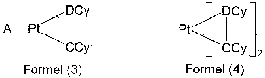 DCy gleich oder verschieden bei jedem Auftreten eine cyclische Gruppe ist, die mindestens ein Donoratom, vorzugsweise Stickstoff, Kohlenstoff in Form eines Carbens oder Phosphor, enthält, über das die cyclische Gruppe an das Metall gebunden ist, und die wiederum einen oder mehrere Substituenten R1 tragen kann; die Gruppen DCy und CCy sind über eine kovalente Bindung miteinander verbunden;CCy gleich oder verschieden bei jedem Auftreten eine cyclische Gruppe ist, die ein Kohlenstoffatom enthält, über das die cyclische Gruppe an das Metall gebunden ist, und die wiederum einen oder mehrere Substituenten R1 tragen kann;A gleich oder verschieden bei jedem Auftreten ein monoanionischer, zweizähniger chelatbildender Ligand, vorzugsweise ein Diketonat-Ligand ist;R1 bei jedem Auftreten gleich oder verschieden sind und F, Cl, Br, I, NO2, CN, eine geradkettige, verzweigte oder cyclische Alkyl- oder Alkoxygruppe mit 1 bis 20 Kohlenstoffatomen, in der eine oder mehrere nicht benachbarte CH2-Gruppen durch -O-, -S-, -NR2-, -CONR2-, -CO-O-, -C=O-, -CH=CH- oder -C≡C- ersetzt sein können und in der ein oder mehrere Wasserstoffatome durch F ersetzt sein können, oder eine Aryl- oder Heteroarylgruppe, die 4 bis 14 Kohlenstoffatome aufweist und durch einen oder mehrere nichtaromatische Reste R1 substituiert sein kann, sind, und eine Mehrzahl von Substituenten R1, entweder am gleichen Ring oder an zwei verschiedenen Ringen, können zusammen wiederum ein mono- oder polycyclisches, aliphatisches oder aromatisches Ringsystem bilden; undR2 bei jedem Auftreten gleich oder verschieden sind und eine geradkettige, verzweigte oder cyclische Alkyl- oder Alkoxygruppe mit 1 bis 20 Kohlenstoffatomen, in der eine oder mehrere nicht benachbarte CH2-Gruppen durch -O-, -S-, -CO-O-, -C=O-, -CH=CH- oder -C≡C- ersetzt sein können und in der ein oder mehrere Wasserstoffatome durch F ersetzt sein können, oder eine Aryl- oder Heteroarylgruppe, die 4 bis 14 Kohlenstoffatome aufweist und durch einen oder mehrere nichtaromatische Reste R1 substituiert sein kann, sind.
 - Zusammensetzung nach einem oder mehreren der Ansprüche 1 bis 11, dadurch gekennzeichnet, dass die Zusammensetzung 0,25 bis 5 Gew.-% organische lichtemittierende Materialien und Ladungstransportmaterialien mit einem Molekulargewicht von höchstens 5000 g/mol enthält.
- Verwendung einer Zusammensetzung nach einem oder mehreren der Ansprüche 1 bis 12 als Beschichtung oder Druckfarbe zur Herstellung von organischen Elektrolumineszenz(EL)-Vorrichtungen, vorzugsweise OLED-Vorrichtungen.
- Organische Elektrolumineszenz-Vorrichtung, vorzugsweise OLED-Vorrichtung, hergestellt aus einer Zusammensetzung nach einem oder mehreren der Ansprüche 1 bis 12.
Priority Applications (1)
| Application Number | Priority Date | Filing Date | Title |
|---|---|---|---|
| EP14799670.6A EP3077475B1 (de) | 2013-12-06 | 2014-11-11 | Zusammensetzungen mit einem polymeren bindemittel mit acryl- und/oder methacrylsäureestereinheiten |
Applications Claiming Priority (3)
| Application Number | Priority Date | Filing Date | Title |
|---|---|---|---|
| EP13005696 | 2013-12-06 | ||
| EP14799670.6A EP3077475B1 (de) | 2013-12-06 | 2014-11-11 | Zusammensetzungen mit einem polymeren bindemittel mit acryl- und/oder methacrylsäureestereinheiten |
| PCT/EP2014/003015 WO2015082037A1 (en) | 2013-12-06 | 2014-11-11 | Compositions containing a polymeric binder which comprises acrylic and/or methacrylic acid ester units |
Publications (2)
| Publication Number | Publication Date |
|---|---|
| EP3077475A1 EP3077475A1 (de) | 2016-10-12 |
| EP3077475B1 true EP3077475B1 (de) | 2018-07-04 |
Family
ID=49752908
Family Applications (1)
| Application Number | Title | Priority Date | Filing Date |
|---|---|---|---|
| EP14799670.6A Active EP3077475B1 (de) | 2013-12-06 | 2014-11-11 | Zusammensetzungen mit einem polymeren bindemittel mit acryl- und/oder methacrylsäureestereinheiten |
Country Status (6)
| Country | Link |
|---|---|
| US (1) | US20160301003A1 (de) |
| EP (1) | EP3077475B1 (de) |
| JP (1) | JP6716457B2 (de) |
| KR (1) | KR20160094430A (de) |
| CN (1) | CN105793387B (de) |
| WO (1) | WO2015082037A1 (de) |
Families Citing this family (1)
| Publication number | Priority date | Publication date | Assignee | Title |
|---|---|---|---|---|
| JP6907197B2 (ja) | 2015-10-09 | 2021-07-21 | メルク パテント ゲーエムベーハー | N,n−ジアルキルアニリン溶媒を含む調合物 |
Family Cites Families (90)
| Publication number | Priority date | Publication date | Assignee | Title |
|---|---|---|---|---|
| US4780536A (en) | 1986-09-05 | 1988-10-25 | The Ohio State University Research Foundation | Hexaazatriphenylene hexanitrile and its derivatives and their preparations |
| US5061569A (en) | 1990-07-26 | 1991-10-29 | Eastman Kodak Company | Electroluminescent device with organic electroluminescent medium |
| JPH061973A (ja) | 1992-06-18 | 1994-01-11 | Konica Corp | 有機エレクトロルミネッセンス素子 |
| WO1995009147A1 (fr) | 1993-09-29 | 1995-04-06 | Idemitsu Kosan Co., Ltd. | Element electroluminescent organique et derive d'arylenediamine |
| EP0650955B1 (de) | 1993-11-01 | 1998-08-19 | Hodogaya Chemical Co., Ltd. | Aminverbindung und sie enthaltende Elektrolumineszenzvorrichtung |
| EP0676461B1 (de) | 1994-04-07 | 2002-08-14 | Covion Organic Semiconductors GmbH | Spiroverbindungen und ihre Verwendung als Elektrolumineszenzmaterialien |
| EP0681019B1 (de) | 1994-04-26 | 1999-09-01 | TDK Corporation | Phenylanthracenderivat und organisches EL-Element |
| WO1998030071A1 (fr) | 1996-12-28 | 1998-07-09 | Tdk Corporation | Elements electroluminescents organiques |
| US5952778A (en) | 1997-03-18 | 1999-09-14 | International Business Machines Corporation | Encapsulated organic light emitting device |
| US5935721A (en) | 1998-03-20 | 1999-08-10 | Eastman Kodak Company | Organic electroluminescent elements for stable electroluminescent |
| DE19812259A1 (de) | 1998-03-20 | 1999-10-21 | Bayer Ag | EL-Anordnung auf Basis von tert.-Aminen, in Alkohol löslichen Alq3-Derivaten bzw. Mischungen und polymeren Bindern |
| DE19825737A1 (de) | 1998-06-09 | 1999-12-16 | Bayer Ag | Elektrolumineszierende Anordnungen mit N-Alkyl-2,2'-imino-bis-(8-hydroxychinolin)-Metallkomplexen |
| JP3302945B2 (ja) | 1998-06-23 | 2002-07-15 | ネースディスプレイ・カンパニー・リミテッド | 新規な有機金属発光物質およびそれを含む有機電気発光素子 |
| JP4429438B2 (ja) | 1999-01-19 | 2010-03-10 | 出光興産株式会社 | アミノ化合物及びそれを用いた有機エレクトロルミネッセンス素子 |
| EP1729327B2 (de) | 1999-05-13 | 2022-08-10 | The Trustees Of Princeton University | Verwendung einer phosphoreszierenden Iridiumverbindung als Emissionsmolekül in einer organischen lichtemittierenden Vorrichtung |
| EP1933395B2 (de) | 1999-12-01 | 2019-08-07 | The Trustees of Princeton University | Komplex der Formel L2IrX |
| KR100377321B1 (ko) | 1999-12-31 | 2003-03-26 | 주식회사 엘지화학 | 피-형 반도체 성질을 갖는 유기 화합물을 포함하는 전기소자 |
| JP4220644B2 (ja) | 2000-02-14 | 2009-02-04 | 三井化学株式会社 | アミン化合物および該化合物を含有する有機電界発光素子 |
| US6660410B2 (en) | 2000-03-27 | 2003-12-09 | Idemitsu Kosan Co., Ltd. | Organic electroluminescence element |
| US20020121638A1 (en) | 2000-06-30 | 2002-09-05 | Vladimir Grushin | Electroluminescent iridium compounds with fluorinated phenylpyridines, phenylpyrimidines, and phenylquinolines and devices made with such compounds |
| EP1325671B1 (de) | 2000-08-11 | 2012-10-24 | The Trustees Of Princeton University | Organometallische verbdindungen und emissionsverschobene organische elektrolumineszens |
| JP4154140B2 (ja) | 2000-09-26 | 2008-09-24 | キヤノン株式会社 | 金属配位化合物 |
| JP4154138B2 (ja) | 2000-09-26 | 2008-09-24 | キヤノン株式会社 | 発光素子、表示装置及び金属配位化合物 |
| JP4154139B2 (ja) | 2000-09-26 | 2008-09-24 | キヤノン株式会社 | 発光素子 |
| KR100691543B1 (ko) | 2002-01-18 | 2007-03-09 | 주식회사 엘지화학 | 새로운 전자 수송용 물질 및 이를 이용한 유기 발광 소자 |
| DE10207859A1 (de) | 2002-02-20 | 2003-09-04 | Univ Dresden Tech | Dotiertes organisches Halbleitermaterial sowie Verfahren zu dessen Herstellung |
| ITRM20020411A1 (it) | 2002-08-01 | 2004-02-02 | Univ Roma La Sapienza | Derivati dello spirobifluorene, loro preparazione e loro uso. |
| KR100924462B1 (ko) | 2002-08-23 | 2009-11-03 | 이데미쓰 고산 가부시키가이샤 | 유기 전기발광 소자 및 안트라센 유도체 |
| JPWO2004028217A1 (ja) | 2002-09-20 | 2006-01-19 | 出光興産株式会社 | 有機エレクトロルミネッセンス素子 |
| US6818919B2 (en) | 2002-09-23 | 2004-11-16 | Air Products And Chemicals, Inc. | Light emitting layers for LED devices based on high Tg polymer matrix compositions |
| DE10249723A1 (de) | 2002-10-25 | 2004-05-06 | Covion Organic Semiconductors Gmbh | Arylamin-Einheiten enthaltende konjugierte Polymere, deren Darstellung und Verwendung |
| JP4287198B2 (ja) | 2002-11-18 | 2009-07-01 | 出光興産株式会社 | 有機エレクトロルミネッセンス素子 |
| JP2006511939A (ja) | 2002-12-23 | 2006-04-06 | コビオン・オーガニック・セミコンダクターズ・ゲーエムベーハー | 有機エレクトロルミネセンス素子 |
| DE10310887A1 (de) | 2003-03-11 | 2004-09-30 | Covion Organic Semiconductors Gmbh | Matallkomplexe |
| KR101020350B1 (ko) | 2003-03-13 | 2011-03-08 | 이데미쓰 고산 가부시키가이샤 | 신규한 질소 함유 헤테로환 유도체 및 이를 이용한 유기 전기발광 소자 |
| JP4411851B2 (ja) | 2003-03-19 | 2010-02-10 | コニカミノルタホールディングス株式会社 | 有機エレクトロルミネッセンス素子 |
| CN1768029B (zh) | 2003-04-10 | 2012-02-08 | 出光兴产株式会社 | 芳香族胺衍生物和采用该衍生物的有机场致发光元件 |
| US7345301B2 (en) | 2003-04-15 | 2008-03-18 | Merck Patent Gmbh | Mixtures of matrix materials and organic semiconductors capable of emission, use of the same and electronic components containing said mixtures |
| EP1617710B1 (de) | 2003-04-23 | 2015-05-20 | Konica Minolta Holdings, Inc. | Material für ein organisches elektrolumineszenzgerät, organisches elektrolumineszenzgerät, beleuchtungsvorrichtung und anzeige |
| US20070103059A1 (en) | 2003-05-16 | 2007-05-10 | Sumitomo Chemical Company, Limited | Composition and polymer light-emitting device |
| GB0311234D0 (en) * | 2003-05-16 | 2003-06-18 | Isis Innovation | Organic phosphorescent material and organic optoelectronic device |
| TWI224473B (en) | 2003-06-03 | 2004-11-21 | Chin-Hsin Chen | Doped co-host emitter system in organic electroluminescent devices |
| DE10345572A1 (de) | 2003-09-29 | 2005-05-19 | Covion Organic Semiconductors Gmbh | Metallkomplexe |
| US7795801B2 (en) | 2003-09-30 | 2010-09-14 | Konica Minolta Holdings, Inc. | Organic electroluminescent element, illuminator, display and compound |
| DE10350722A1 (de) | 2003-10-30 | 2005-05-25 | Covion Organic Semiconductors Gmbh | Metallkomplexe |
| ATE475971T1 (de) | 2003-11-28 | 2010-08-15 | Merck Patent Gmbh | Organische halbleiterschicht-formulierungen mit polyacenen und organischen binderpolymeren |
| DE10357044A1 (de) | 2003-12-04 | 2005-07-14 | Novaled Gmbh | Verfahren zur Dotierung von organischen Halbleitern mit Chinondiiminderivaten |
| US7252893B2 (en) | 2004-02-17 | 2007-08-07 | Eastman Kodak Company | Anthracene derivative host having ranges of dopants |
| DE102004008304A1 (de) | 2004-02-20 | 2005-09-08 | Covion Organic Semiconductors Gmbh | Organische elektronische Vorrichtungen |
| US7326371B2 (en) | 2004-03-25 | 2008-02-05 | Eastman Kodak Company | Electroluminescent device with anthracene derivative host |
| US7790890B2 (en) | 2004-03-31 | 2010-09-07 | Konica Minolta Holdings, Inc. | Organic electroluminescence element material, organic electroluminescence element, display device and illumination device |
| KR100787425B1 (ko) | 2004-11-29 | 2007-12-26 | 삼성에스디아이 주식회사 | 페닐카바졸계 화합물 및 이를 이용한 유기 전계 발광 소자 |
| DE102004023277A1 (de) | 2004-05-11 | 2005-12-01 | Covion Organic Semiconductors Gmbh | Neue Materialmischungen für die Elektrolumineszenz |
| EP1749014B1 (de) | 2004-05-19 | 2010-07-07 | Merck Patent GmbH | Metallkomplexe |
| TWI327563B (en) | 2004-05-24 | 2010-07-21 | Au Optronics Corp | Anthracene compound and organic electroluminescent device including the anthracene compound |
| JP4862248B2 (ja) | 2004-06-04 | 2012-01-25 | コニカミノルタホールディングス株式会社 | 有機エレクトロルミネッセンス素子、照明装置及び表示装置 |
| TW200613515A (en) | 2004-06-26 | 2006-05-01 | Merck Patent Gmbh | Compounds for organic electronic devices |
| DE102004031000A1 (de) | 2004-06-26 | 2006-01-12 | Covion Organic Semiconductors Gmbh | Organische Elektrolumineszenzvorrichtungen |
| ITRM20040352A1 (it) | 2004-07-15 | 2004-10-15 | Univ Roma La Sapienza | Derivati oligomerici dello spirobifluorene, loro preparazione e loro uso. |
| DE102004034517A1 (de) | 2004-07-16 | 2006-02-16 | Covion Organic Semiconductors Gmbh | Metallkomplexe |
| EP1655359A1 (de) | 2004-11-06 | 2006-05-10 | Covion Organic Semiconductors GmbH | Organische Elektrolumineszenzvorrichtung |
| TW200639140A (en) | 2004-12-01 | 2006-11-16 | Merck Patent Gmbh | Compounds for organic electronic devices |
| TW200634020A (en) | 2004-12-09 | 2006-10-01 | Merck Patent Gmbh | Metal complexes |
| KR101192463B1 (ko) | 2005-01-05 | 2012-10-17 | 이데미쓰 고산 가부시키가이샤 | 방향족 아민 유도체 및 이를 이용한 유기 전기발광 소자 |
| JP2008528646A (ja) | 2005-02-03 | 2008-07-31 | メルク パテント ゲーエムベーハー | 金属錯体 |
| JP2006253445A (ja) | 2005-03-11 | 2006-09-21 | Toyo Ink Mfg Co Ltd | 有機エレクトロルミネッセンス素子 |
| JP4263700B2 (ja) | 2005-03-15 | 2009-05-13 | 出光興産株式会社 | 芳香族アミン誘導体及びそれを用いた有機エレクトロルミネッセンス素子 |
| JP4358884B2 (ja) | 2005-03-18 | 2009-11-04 | 出光興産株式会社 | 芳香族アミン誘導体及びそれを用いた有機エレクトロルミネッセンス素子 |
| JP5242380B2 (ja) | 2005-05-03 | 2013-07-24 | メルク パテント ゲーエムベーハー | 有機エレクトロルミネッセンス素子 |
| DE102005023437A1 (de) | 2005-05-20 | 2006-11-30 | Merck Patent Gmbh | Verbindungen für organische elektronische Vorrichtungen |
| EP1956022B1 (de) | 2005-12-01 | 2012-07-25 | Nippon Steel Chemical Co., Ltd. | Verbindung für organisches elektrolumineszentes element und organisches elektrolumineszentes element |
| DE102005058543A1 (de) | 2005-12-08 | 2007-06-14 | Merck Patent Gmbh | Organische Elektrolumineszenzvorrichtungen |
| DE102005058557A1 (de) | 2005-12-08 | 2007-06-14 | Merck Patent Gmbh | Organische Elektrolumineszenzvorrichtung |
| US8440324B2 (en) * | 2005-12-27 | 2013-05-14 | E I Du Pont De Nemours And Company | Compositions comprising novel copolymers and electronic devices made with such compositions |
| DE102006015183A1 (de) | 2006-04-01 | 2007-10-04 | Merck Patent Gmbh | Materialien für organische Elektrolumineszenzvorrichtungen |
| DE102006025777A1 (de) | 2006-05-31 | 2007-12-06 | Merck Patent Gmbh | Neue Materialien für organische Elektrolumineszenzvorrichtungen |
| DE102006025846A1 (de) | 2006-06-02 | 2007-12-06 | Merck Patent Gmbh | Neue Materialien für organische Elektrolumineszenzvorrichtungen |
| DE102006031990A1 (de) | 2006-07-11 | 2008-01-17 | Merck Patent Gmbh | Neue Materialien für organische Elektrolumineszenzvorrichtungen |
| EP1883124A1 (de) | 2006-07-27 | 2008-01-30 | IEE INTERNATIONAL ELECTRONICS & ENGINEERING S.A. | Verbindung für organisches lichtemittierendes Material |
| JP4388590B2 (ja) | 2006-11-09 | 2009-12-24 | 新日鐵化学株式会社 | 有機電界発光素子用化合物及び有機電界発光素子 |
| DE102007002714A1 (de) | 2007-01-18 | 2008-07-31 | Merck Patent Gmbh | Neue Materialien für organische Elektrolumineszenzvorrichtungen |
| US20080258111A1 (en) * | 2007-04-17 | 2008-10-23 | General Electric Company | Polycarbazolyl(meth)acrylate light emissive compositions |
| DE102007024850A1 (de) | 2007-05-29 | 2008-12-04 | Merck Patent Gmbh | Neue Materialien für organische Elektrolumineszenzvorrichtungen |
| DE102007053771A1 (de) | 2007-11-12 | 2009-05-14 | Merck Patent Gmbh | Organische Elektrolumineszenzvorrichtungen |
| DE102008027005A1 (de) | 2008-06-05 | 2009-12-10 | Merck Patent Gmbh | Organische elektronische Vorrichtung enthaltend Metallkomplexe |
| DE102008033943A1 (de) | 2008-07-18 | 2010-01-21 | Merck Patent Gmbh | Neue Materialien für organische Elektrolumineszenzvorrichtungen |
| DE102008035413A1 (de) | 2008-07-29 | 2010-02-04 | Merck Patent Gmbh | Verbindungen für organische elektronische Vorrichtungen |
| DE102008036982A1 (de) | 2008-08-08 | 2010-02-11 | Merck Patent Gmbh | Organische Elektrolumineszenzvorrichtung |
| US9178156B2 (en) * | 2009-12-23 | 2015-11-03 | Merck Patent Gmbh | Compositions comprising polymeric binders |
| WO2012132863A1 (ja) * | 2011-03-29 | 2012-10-04 | 凸版印刷株式会社 | インク組成物とそれを用いた有機el素子及びその製造方法 |
-
2014
- 2014-11-11 US US15/101,066 patent/US20160301003A1/en not_active Abandoned
- 2014-11-11 CN CN201480065940.7A patent/CN105793387B/zh active Active
- 2014-11-11 WO PCT/EP2014/003015 patent/WO2015082037A1/en active Application Filing
- 2014-11-11 EP EP14799670.6A patent/EP3077475B1/de active Active
- 2014-11-11 JP JP2016536834A patent/JP6716457B2/ja active Active
- 2014-11-11 KR KR1020167017870A patent/KR20160094430A/ko not_active IP Right Cessation
Non-Patent Citations (1)
| Title |
|---|
| None * |
Also Published As
| Publication number | Publication date |
|---|---|
| JP2017501263A (ja) | 2017-01-12 |
| CN105793387B (zh) | 2019-04-30 |
| JP6716457B2 (ja) | 2020-07-01 |
| EP3077475A1 (de) | 2016-10-12 |
| KR20160094430A (ko) | 2016-08-09 |
| CN105793387A (zh) | 2016-07-20 |
| US20160301003A1 (en) | 2016-10-13 |
| WO2015082037A1 (en) | 2015-06-11 |
Similar Documents
| Publication | Publication Date | Title |
|---|---|---|
| EP2517274B1 (de) | Zusammensetzungen mit polymerbindern | |
| KR102045196B1 (ko) | 개선된 성능을 갖는 조성물 | |
| EP2517273B1 (de) | Zusammensetzungen mit organischen halbleiterverbindungen | |
| EP2559079B1 (de) | Zusammensetzung und verfahren zur herstellung organischer elektronischer vorrichtungen | |
| US11309493B2 (en) | Formulations with a low particle content | |
| EP3077475B1 (de) | Zusammensetzungen mit einem polymeren bindemittel mit acryl- und/oder methacrylsäureestereinheiten | |
| TWI813576B (zh) | 具有低含量苯酚類雜質的調配物 |
Legal Events
| Date | Code | Title | Description |
|---|---|---|---|
| PUAI | Public reference made under article 153(3) epc to a published international application that has entered the european phase |
Free format text: ORIGINAL CODE: 0009012 |
|
| 17P | Request for examination filed |
Effective date: 20160408 |
|
| AK | Designated contracting states |
Kind code of ref document: A1 Designated state(s): AL AT BE BG CH CY CZ DE DK EE ES FI FR GB GR HR HU IE IS IT LI LT LU LV MC MK MT NL NO PL PT RO RS SE SI SK SM TR |
|
| AX | Request for extension of the european patent |
Extension state: BA ME |
|
| RIN1 | Information on inventor provided before grant (corrected) |
Inventor name: LEONHARD, CHRISTOPH Inventor name: MAY, PHILIP EDWARD Inventor name: PAN, JUNYOU Inventor name: LUDEMANN, AURELIE |
|
| DAX | Request for extension of the european patent (deleted) | ||
| 17Q | First examination report despatched |
Effective date: 20170327 |
|
| GRAP | Despatch of communication of intention to grant a patent |
Free format text: ORIGINAL CODE: EPIDOSNIGR1 |
|
| INTG | Intention to grant announced |
Effective date: 20180316 |
|
| GRAS | Grant fee paid |
Free format text: ORIGINAL CODE: EPIDOSNIGR3 |
|
| GRAA | (expected) grant |
Free format text: ORIGINAL CODE: 0009210 |
|
| AK | Designated contracting states |
Kind code of ref document: B1 Designated state(s): AL AT BE BG CH CY CZ DE DK EE ES FI FR GB GR HR HU IE IS IT LI LT LU LV MC MK MT NL NO PL PT RO RS SE SI SK SM TR |
|
| REG | Reference to a national code |
Ref country code: GB Ref legal event code: FG4D |
|
| REG | Reference to a national code |
Ref country code: CH Ref legal event code: EP |
|
| REG | Reference to a national code |
Ref country code: AT Ref legal event code: REF Ref document number: 1014502 Country of ref document: AT Kind code of ref document: T Effective date: 20180715 |
|
| REG | Reference to a national code |
Ref country code: IE Ref legal event code: FG4D |
|
| REG | Reference to a national code |
Ref country code: DE Ref legal event code: R096 Ref document number: 602014027973 Country of ref document: DE |
|
| REG | Reference to a national code |
Ref country code: NL Ref legal event code: MP Effective date: 20180704 |
|
| REG | Reference to a national code |
Ref country code: LT Ref legal event code: MG4D |
|
| REG | Reference to a national code |
Ref country code: AT Ref legal event code: MK05 Ref document number: 1014502 Country of ref document: AT Kind code of ref document: T Effective date: 20180704 |
|
| PG25 | Lapsed in a contracting state [announced via postgrant information from national office to epo] |
Ref country code: NL Free format text: LAPSE BECAUSE OF FAILURE TO SUBMIT A TRANSLATION OF THE DESCRIPTION OR TO PAY THE FEE WITHIN THE PRESCRIBED TIME-LIMIT Effective date: 20180704 |
|
| PG25 | Lapsed in a contracting state [announced via postgrant information from national office to epo] |
Ref country code: FI Free format text: LAPSE BECAUSE OF FAILURE TO SUBMIT A TRANSLATION OF THE DESCRIPTION OR TO PAY THE FEE WITHIN THE PRESCRIBED TIME-LIMIT Effective date: 20180704 Ref country code: CZ Free format text: LAPSE BECAUSE OF FAILURE TO SUBMIT A TRANSLATION OF THE DESCRIPTION OR TO PAY THE FEE WITHIN THE PRESCRIBED TIME-LIMIT Effective date: 20180704 Ref country code: LT Free format text: LAPSE BECAUSE OF FAILURE TO SUBMIT A TRANSLATION OF THE DESCRIPTION OR TO PAY THE FEE WITHIN THE PRESCRIBED TIME-LIMIT Effective date: 20180704 Ref country code: PL Free format text: LAPSE BECAUSE OF FAILURE TO SUBMIT A TRANSLATION OF THE DESCRIPTION OR TO PAY THE FEE WITHIN THE PRESCRIBED TIME-LIMIT Effective date: 20180704 Ref country code: GR Free format text: LAPSE BECAUSE OF FAILURE TO SUBMIT A TRANSLATION OF THE DESCRIPTION OR TO PAY THE FEE WITHIN THE PRESCRIBED TIME-LIMIT Effective date: 20181005 Ref country code: SE Free format text: LAPSE BECAUSE OF FAILURE TO SUBMIT A TRANSLATION OF THE DESCRIPTION OR TO PAY THE FEE WITHIN THE PRESCRIBED TIME-LIMIT Effective date: 20180704 Ref country code: BG Free format text: LAPSE BECAUSE OF FAILURE TO SUBMIT A TRANSLATION OF THE DESCRIPTION OR TO PAY THE FEE WITHIN THE PRESCRIBED TIME-LIMIT Effective date: 20181004 Ref country code: IS Free format text: LAPSE BECAUSE OF FAILURE TO SUBMIT A TRANSLATION OF THE DESCRIPTION OR TO PAY THE FEE WITHIN THE PRESCRIBED TIME-LIMIT Effective date: 20181104 Ref country code: RS Free format text: LAPSE BECAUSE OF FAILURE TO SUBMIT A TRANSLATION OF THE DESCRIPTION OR TO PAY THE FEE WITHIN THE PRESCRIBED TIME-LIMIT Effective date: 20180704 Ref country code: AT Free format text: LAPSE BECAUSE OF FAILURE TO SUBMIT A TRANSLATION OF THE DESCRIPTION OR TO PAY THE FEE WITHIN THE PRESCRIBED TIME-LIMIT Effective date: 20180704 Ref country code: NO Free format text: LAPSE BECAUSE OF FAILURE TO SUBMIT A TRANSLATION OF THE DESCRIPTION OR TO PAY THE FEE WITHIN THE PRESCRIBED TIME-LIMIT Effective date: 20181004 |
|
| PG25 | Lapsed in a contracting state [announced via postgrant information from national office to epo] |
Ref country code: HR Free format text: LAPSE BECAUSE OF FAILURE TO SUBMIT A TRANSLATION OF THE DESCRIPTION OR TO PAY THE FEE WITHIN THE PRESCRIBED TIME-LIMIT Effective date: 20180704 Ref country code: AL Free format text: LAPSE BECAUSE OF FAILURE TO SUBMIT A TRANSLATION OF THE DESCRIPTION OR TO PAY THE FEE WITHIN THE PRESCRIBED TIME-LIMIT Effective date: 20180704 Ref country code: ES Free format text: LAPSE BECAUSE OF FAILURE TO SUBMIT A TRANSLATION OF THE DESCRIPTION OR TO PAY THE FEE WITHIN THE PRESCRIBED TIME-LIMIT Effective date: 20180704 Ref country code: LV Free format text: LAPSE BECAUSE OF FAILURE TO SUBMIT A TRANSLATION OF THE DESCRIPTION OR TO PAY THE FEE WITHIN THE PRESCRIBED TIME-LIMIT Effective date: 20180704 |
|
| REG | Reference to a national code |
Ref country code: DE Ref legal event code: R097 Ref document number: 602014027973 Country of ref document: DE |
|
| PG25 | Lapsed in a contracting state [announced via postgrant information from national office to epo] |
Ref country code: RO Free format text: LAPSE BECAUSE OF FAILURE TO SUBMIT A TRANSLATION OF THE DESCRIPTION OR TO PAY THE FEE WITHIN THE PRESCRIBED TIME-LIMIT Effective date: 20180704 Ref country code: IT Free format text: LAPSE BECAUSE OF FAILURE TO SUBMIT A TRANSLATION OF THE DESCRIPTION OR TO PAY THE FEE WITHIN THE PRESCRIBED TIME-LIMIT Effective date: 20180704 Ref country code: EE Free format text: LAPSE BECAUSE OF FAILURE TO SUBMIT A TRANSLATION OF THE DESCRIPTION OR TO PAY THE FEE WITHIN THE PRESCRIBED TIME-LIMIT Effective date: 20180704 |
|
| PLBE | No opposition filed within time limit |
Free format text: ORIGINAL CODE: 0009261 |
|
| STAA | Information on the status of an ep patent application or granted ep patent |
Free format text: STATUS: NO OPPOSITION FILED WITHIN TIME LIMIT |
|
| PG25 | Lapsed in a contracting state [announced via postgrant information from national office to epo] |
Ref country code: DK Free format text: LAPSE BECAUSE OF FAILURE TO SUBMIT A TRANSLATION OF THE DESCRIPTION OR TO PAY THE FEE WITHIN THE PRESCRIBED TIME-LIMIT Effective date: 20180704 Ref country code: SK Free format text: LAPSE BECAUSE OF FAILURE TO SUBMIT A TRANSLATION OF THE DESCRIPTION OR TO PAY THE FEE WITHIN THE PRESCRIBED TIME-LIMIT Effective date: 20180704 Ref country code: SM Free format text: LAPSE BECAUSE OF FAILURE TO SUBMIT A TRANSLATION OF THE DESCRIPTION OR TO PAY THE FEE WITHIN THE PRESCRIBED TIME-LIMIT Effective date: 20180704 |
|
| 26N | No opposition filed |
Effective date: 20190405 |
|
| REG | Reference to a national code |
Ref country code: CH Ref legal event code: PL |
|
| GBPC | Gb: european patent ceased through non-payment of renewal fee |
Effective date: 20181111 |
|
| PG25 | Lapsed in a contracting state [announced via postgrant information from national office to epo] |
Ref country code: MC Free format text: LAPSE BECAUSE OF FAILURE TO SUBMIT A TRANSLATION OF THE DESCRIPTION OR TO PAY THE FEE WITHIN THE PRESCRIBED TIME-LIMIT Effective date: 20180704 Ref country code: LU Free format text: LAPSE BECAUSE OF NON-PAYMENT OF DUE FEES Effective date: 20181111 |
|
| REG | Reference to a national code |
Ref country code: BE Ref legal event code: MM Effective date: 20181130 |
|
| REG | Reference to a national code |
Ref country code: IE Ref legal event code: MM4A |
|
| PG25 | Lapsed in a contracting state [announced via postgrant information from national office to epo] |
Ref country code: LI Free format text: LAPSE BECAUSE OF NON-PAYMENT OF DUE FEES Effective date: 20181130 Ref country code: CH Free format text: LAPSE BECAUSE OF NON-PAYMENT OF DUE FEES Effective date: 20181130 Ref country code: SI Free format text: LAPSE BECAUSE OF FAILURE TO SUBMIT A TRANSLATION OF THE DESCRIPTION OR TO PAY THE FEE WITHIN THE PRESCRIBED TIME-LIMIT Effective date: 20180704 |
|
| PG25 | Lapsed in a contracting state [announced via postgrant information from national office to epo] |
Ref country code: IE Free format text: LAPSE BECAUSE OF NON-PAYMENT OF DUE FEES Effective date: 20181111 Ref country code: FR Free format text: LAPSE BECAUSE OF NON-PAYMENT OF DUE FEES Effective date: 20181130 |
|
| PG25 | Lapsed in a contracting state [announced via postgrant information from national office to epo] |
Ref country code: BE Free format text: LAPSE BECAUSE OF NON-PAYMENT OF DUE FEES Effective date: 20181130 |
|
| PG25 | Lapsed in a contracting state [announced via postgrant information from national office to epo] |
Ref country code: GB Free format text: LAPSE BECAUSE OF NON-PAYMENT OF DUE FEES Effective date: 20181111 |
|
| PG25 | Lapsed in a contracting state [announced via postgrant information from national office to epo] |
Ref country code: MT Free format text: LAPSE BECAUSE OF NON-PAYMENT OF DUE FEES Effective date: 20181111 |
|
| PG25 | Lapsed in a contracting state [announced via postgrant information from national office to epo] |
Ref country code: TR Free format text: LAPSE BECAUSE OF FAILURE TO SUBMIT A TRANSLATION OF THE DESCRIPTION OR TO PAY THE FEE WITHIN THE PRESCRIBED TIME-LIMIT Effective date: 20180704 |
|
| PG25 | Lapsed in a contracting state [announced via postgrant information from national office to epo] |
Ref country code: PT Free format text: LAPSE BECAUSE OF FAILURE TO SUBMIT A TRANSLATION OF THE DESCRIPTION OR TO PAY THE FEE WITHIN THE PRESCRIBED TIME-LIMIT Effective date: 20180704 |
|
| PG25 | Lapsed in a contracting state [announced via postgrant information from national office to epo] |
Ref country code: HU Free format text: LAPSE BECAUSE OF FAILURE TO SUBMIT A TRANSLATION OF THE DESCRIPTION OR TO PAY THE FEE WITHIN THE PRESCRIBED TIME-LIMIT; INVALID AB INITIO Effective date: 20141111 Ref country code: MK Free format text: LAPSE BECAUSE OF NON-PAYMENT OF DUE FEES Effective date: 20180704 Ref country code: CY Free format text: LAPSE BECAUSE OF FAILURE TO SUBMIT A TRANSLATION OF THE DESCRIPTION OR TO PAY THE FEE WITHIN THE PRESCRIBED TIME-LIMIT Effective date: 20180704 |
|
| P01 | Opt-out of the competence of the unified patent court (upc) registered |
Effective date: 20230518 |
|
| PGFP | Annual fee paid to national office [announced via postgrant information from national office to epo] |
Ref country code: DE Payment date: 20230919 Year of fee payment: 10 |