EP1555690A1 - Eingefügtes soi-substrat, prozess zu seiner herstellung und halbleiterbauelement - Google Patents
Eingefügtes soi-substrat, prozess zu seiner herstellung und halbleiterbauelement Download PDFInfo
- Publication number
- EP1555690A1 EP1555690A1 EP03809450A EP03809450A EP1555690A1 EP 1555690 A1 EP1555690 A1 EP 1555690A1 EP 03809450 A EP03809450 A EP 03809450A EP 03809450 A EP03809450 A EP 03809450A EP 1555690 A1 EP1555690 A1 EP 1555690A1
- Authority
- EP
- European Patent Office
- Prior art keywords
- wafer
- soi
- bonded
- active layer
- layer
- Prior art date
- Legal status (The legal status is an assumption and is not a legal conclusion. Google has not performed a legal analysis and makes no representation as to the accuracy of the status listed.)
- Granted
Links
Images




Classifications
-
- H—ELECTRICITY
- H10—SEMICONDUCTOR DEVICES; ELECTRIC SOLID-STATE DEVICES NOT OTHERWISE PROVIDED FOR
- H10D—INORGANIC ELECTRIC SEMICONDUCTOR DEVICES
- H10D86/00—Integrated devices formed in or on insulating or conducting substrates, e.g. formed in silicon-on-insulator [SOI] substrates or on stainless steel or glass substrates
-
- H—ELECTRICITY
- H10—SEMICONDUCTOR DEVICES; ELECTRIC SOLID-STATE DEVICES NOT OTHERWISE PROVIDED FOR
- H10W—GENERIC PACKAGES, INTERCONNECTIONS, CONNECTORS OR OTHER CONSTRUCTIONAL DETAILS OF DEVICES COVERED BY CLASS H10
- H10W10/00—Isolation regions in semiconductor bodies between components of integrated devices
- H10W10/20—Air gaps
-
- H—ELECTRICITY
- H10—SEMICONDUCTOR DEVICES; ELECTRIC SOLID-STATE DEVICES NOT OTHERWISE PROVIDED FOR
- H10P—GENERIC PROCESSES OR APPARATUS FOR THE MANUFACTURE OR TREATMENT OF DEVICES COVERED BY CLASS H10
- H10P90/00—Preparation of wafers not covered by a single main group of this subclass, e.g. wafer reinforcement
- H10P90/19—Preparing inhomogeneous wafers
- H10P90/1904—Preparing vertically inhomogeneous wafers
- H10P90/1906—Preparing SOI wafers
- H10P90/1914—Preparing SOI wafers using bonding
-
- H—ELECTRICITY
- H10—SEMICONDUCTOR DEVICES; ELECTRIC SOLID-STATE DEVICES NOT OTHERWISE PROVIDED FOR
- H10P—GENERIC PROCESSES OR APPARATUS FOR THE MANUFACTURE OR TREATMENT OF DEVICES COVERED BY CLASS H10
- H10P90/00—Preparation of wafers not covered by a single main group of this subclass, e.g. wafer reinforcement
- H10P90/19—Preparing inhomogeneous wafers
- H10P90/1904—Preparing vertically inhomogeneous wafers
- H10P90/1906—Preparing SOI wafers
- H10P90/1914—Preparing SOI wafers using bonding
- H10P90/1916—Preparing SOI wafers using bonding with separation or delamination along an ion implanted layer, e.g. Smart-cut
-
- H—ELECTRICITY
- H10—SEMICONDUCTOR DEVICES; ELECTRIC SOLID-STATE DEVICES NOT OTHERWISE PROVIDED FOR
- H10W—GENERIC PACKAGES, INTERCONNECTIONS, CONNECTORS OR OTHER CONSTRUCTIONAL DETAILS OF DEVICES COVERED BY CLASS H10
- H10W10/00—Isolation regions in semiconductor bodies between components of integrated devices
- H10W10/01—Manufacture or treatment
- H10W10/021—Manufacture or treatment of air gaps
-
- H—ELECTRICITY
- H10—SEMICONDUCTOR DEVICES; ELECTRIC SOLID-STATE DEVICES NOT OTHERWISE PROVIDED FOR
- H10W—GENERIC PACKAGES, INTERCONNECTIONS, CONNECTORS OR OTHER CONSTRUCTIONAL DETAILS OF DEVICES COVERED BY CLASS H10
- H10W10/00—Isolation regions in semiconductor bodies between components of integrated devices
- H10W10/10—Isolation regions comprising dielectric materials
- H10W10/181—Semiconductor-on-insulator [SOI] isolation regions, e.g. buried oxide regions of SOI wafers
Definitions
- the present invention relates to a bonded SOI substrate and a manufacturing method thereof and a semiconductor device using said substrate, and more specifically to a technology in which after an active layer wafer and a supporting substrate wafer having been bonded to each other with an insulation layer interposed between them, the active layer wafer is thinned to define a SOI layer.
- a SOI (Silicon On Insulator) substrate has been known as a solution to the problem of separation among such elements.
- the SOI substrate comprises a SOI layer in which a device is to be formed, and a supporting substrate wafer for supporting said SOI layer, wherein a buried silicon oxide film having a thickness of several ⁇ m is disposed between the SOI layer and the supporting substrate wafer.
- This SOI substrate can facilitate the high integration of the device, including the multi-functionality using a three dimensional structure, provide reduced soft errors and higher reliability, and also suppress consumption of electric power.
- a semiconductor substrate As disclosed in the Japanese Patent Laid-open Publication No. 2001-144276.
- a two-dimensional array of a plurality of trenches (recesses) is formed on surface of silicon substrate, which in turn is heat-treated to thereby induce a migration of silicon atoms in the surface layer of the substrate, causing inner walls in the openings of said respective trenches to be coupled with each other to define a device forming area (i.e., SOI layer), while causing inner portions of respective trenches to be coupled to each other to define a plate-like cavity (i.e., insulation layer).
- the inventors have devoted themselves in an enthusiastic research and recognized the importance of the bonded SOI substrate. That is, they have made the present invention based on the finding that during manufacturing of the bonded SOI substrate, if a recessed portion is formed in the surface of the active layer wafer and/or in the surface of the supporting substrate wafer and then said active layer wafer and said supporting substrate wafer are bonded to each other with said surfaces serving as the bonding surfaces, then such a SOI substrate can be fabricated that has a cavity formed inside thereof substantially in accordance with the specified design.
- an object of the present invention is to provide a bonded SOI substrate and a manufacturing method thereof, which allows a cavity of higher dimensional precision to be buried therein as an insulation layer.
- Another object of the present invention is to provide a bonded SOI substrate and a manufacturing method thereof, which allows MOS elements and bipolar elements to be arranged in a mixed manner on the same chip.
- a first invention provides a SOI substrate comprising: a SOI layer in which a device is to be formed; and a supporting substrate wafer for supporting said SOI layer, said SOI layer and said supporting substrate wafer having been bonded to each other with an insulation layer interposed therebetween, in which said insulation layer includes a cavity.
- the SOI wafer and the supporting substrate wafer a variety type of wafers may be employed, including, for example, a single-crystal silicon wafer and a gallium-arsenide wafer.
- the type of the device to be formed in the SOI layer may not be limited.
- the device may include, for example, a MOS type element, a bipolar element, a variety type of diodes and a variety type of transistors, a memory and a processor for further applications, and a variety type of digital circuits and a variety type of analog circuits for yet further applications.
- the thickness of the SOI layer may not be limited.
- the SOI layer of thicker film may be 20 ⁇ m to 50 ⁇ m thick.
- the SOI layer of thinner film may be 0.01 ⁇ m to 20 ⁇ m thick.
- the cavity may be formed substantially across the entire region in the plane of the SOI layer. Alternatively, the cavity may be formed partially in the plane.
- the shape of the cavity may be circular, elliptical, triangular, rectangular or other polygonal shape in plan view.
- the height of the cavity (the length in the thickness direction of the substrate) may be in a range of 0.01 ⁇ m to 50 ⁇ m, preferably in a range of 0.01 ⁇ m to 5 ⁇ m.
- the SOI substrate having the cavity serving as the insulation layer can be easily obtained. Consequently, the degree of freedom in shape and location of the cavity may be extended. Further, designing of a desired device, circuit and the like may be facilitated. For example, such a semiconductor device including the MOS elements and the bipolar elements disposed in a mixed manner can be easily fabricated.
- a second invention provides a SOI substrate in accordance with the first invention, in which said cavity is formed at a plurality of locations in a plane of said bonded SOI substrate.
- the cavity may be formed in response to a design of the desired device, circuit and the like.
- a third invention provides a SOI substrate in accordance with the first or the second invention, in which said insulation layer has a plurality of cavities defined by different heights.
- the cavities may be formed in the bonding surface of the SOI layer or/and in the bonding surface of the supporting substrate wafer.
- the insulation film may be formed in both bonding surfaces of the SOI layer and the supporting substrate wafer.
- the surface on which the insulation film is to be formed is not limited to the bonding surface of the SOI layer and/or the supporting substrate wafer. It may be formed, for example, across the entire surface of the SOI layer and/or the supporting substrate wafer.
- a fourth invention provides a SOI substrate in accordance with the first invention, in which said SOI layer has varied thickness in the plane thereof.
- Each suitable element may be formed in each region of varied thickness.
- Fifth invention provides a manufacturing method of a SOI substrate, comprising: a recessed portion forming step for forming a recessed portion in a surface of an active layer wafer and/or in a surface of a supporting substrate wafer; a bonding step for bonding said active layer wafer and said supporting substrate wafer to each other with said surface(s) having said recessed portion(s) formed therein serving as bonding surface(s) to thereby form a cavity; and a thinning step for thinning said active layer wafer of said bonded wafers to thereby form a SOI layer.
- the location where the recessed portion is formed may be in the surface of the active layer wafer. Alternatively, it may be in the surface of the supporting substrate wafer. Further, the recessed portion may be formed in both surfaces of the active layer wafer and the supporting substrate wafer.
- a variety of techniques including the photolithography, for example, may be used.
- a depth, an extent and a shape of the recessed portion may be arbitrarily determined.
- a patterning mask having a patterned hole defining the same configuration as of the recessed portion is placed over the top of the wafer in which the recessed portion is to be formed, and then said wafer is etched by a predetermined etching method through the patterned hole to form a recessed portion on the surface of the wafer.
- the type of etching method may not be limited.
- the acid etching using a mixed acid of hydrofluoric acid mixed with nitric acid or the alkali etching using NaOH or KOH may be employed.
- a variety of dry etching may be employed.
- this recessed portion can be also formed by the method other than the etching. That is, the wafer surface in the region other than the recessed portion may be raised by a variety type of thin film deposition methods thus to define a relatively recessed portion. Specifically, a mask having a patterned hole encompassing the region excluding that for forming this recessed portion is formed by the photolithography on top of the wafer in which the recessed portion is to be formed. After that, a thin film is formed over the wafer surface by a predetermined thin film deposition method via this patterned hole. Subsequently, in this method, the mask is removed to make the recessed portion of specified dimension emerge in the surface of the wafer.
- the thin film deposition method may include, for example, the spattering method, the vacuum deposition method, the CVD method and the epitaxial growth method.
- the bonding of the active layer wafer with the supporting substrate wafer may be achieved, for example, by bonding the two wafers to each other at a room temperature and then applying the bonding heat treatment thereto.
- the heating temperature in this bonding heat treatment may be 800°C or higher, 1100°C, for example.
- the time period of the bonding heat treatment may be two hours, for example.
- the atmospheric gas in the thermal oxidation furnace to be used may employ oxygen and the like.
- the thinning method of the active layer wafer for example, such a method may be employed in which light elements such as hydrogen ions are implanted into the active layer wafer from its thermally oxidized surface side, and then the active layer wafer and the supporting substrate wafer are bonded to each other and heat treated.
- the smart-cut method may be employed, in which an unnecessary portion of the active layer wafer is separated from the region where the hydrogen ions have been implanted.
- the thinning method by the surface grinding and the surface polishing may be employed, for example.
- the etch stop method may be employed.
- the surface grinding is applied to the active layer wafer side of the bonded wafer, and then thus surface-ground surface is further applied with the surface polishing to thereby produce the SOI layer.
- the surface grinding wheel may be used.
- the polishing for example, the polishing by the polishing machine may be employed. That is, after having been processed with the surface grinding, the bonded wafer is mounted on a polishing head and polished in the condition where the ground surface of the active layer wafer is pressed against polishing cloth affixed on a turn table while supplying a polishing agent (slurry) containing loose abrasive in a polishing liquid.
- the thinning of the active layer wafer may be accomplished exclusively by the surface polishing. In that case, adjusting of the polishing condition for the active layer wafer may be required.
- polishing machine a single type wafer polishing machine or a batch type wafer polishing machine may be used. Further, either a wax type single side polishing machine or a waxless type polishing machine may be used.
- the polishing cloth may be employed, for example, a porous non-woven type polishing cloth made of polyester felt impregnated with polyurethane, an expanded urethane type polishing cloth made by slicing a block of expanded urethane and a suede type polishing cloth made by laminating expanded polyurethane on top of a base material of polyester felt impregnated with polyurethane and then removing the surface layer portion of said polyurethane to resultantly form an opening in the layer of expanded polyurethane.
- a porous non-woven type polishing cloth made of polyester felt impregnated with polyurethane an expanded urethane type polishing cloth made by slicing a block of expanded urethane
- a suede type polishing cloth made by laminating expanded polyurethane on top of a base material of polyester felt impregnated with polyurethane and then removing the surface layer portion of said polyurethane to resultantly form an opening in the layer of expanded polyurethane.
- the recessed portion is formed in the surface of the active layer wafer and/or in the bonding surface of the supporting substrate wafer, and secondly the two wafers are bonded to each other.
- the cavity of highly precise dimension can be buried and formed as the insulation layer.
- the cavities can be simultaneously made in a plurality of locations in the substrate plane, and more advantageously the thickness of the SOI layer defined by those cavities can be arbitrarily determined in an easy manner. Therefore, for example, such a semiconductor device including the MOS type elements and the bipolar elements that are loaded in a mixed manner on the same chip can be fabricated easily.
- a sixth invention provides a manufacturing method of a bonded SOI substrate in accordance with the fifth invention, in which in said recessed portion forming step, said cavity is formed in a plurality of locations in the surface of said active layer wafer and/or in the surface of said supporting substrate wafer.
- a seventh invention provides a manufacturing method of a bonded SOI substrate in accordance with the fifth or the sixth invention, in which in said recessed portion forming step, a plurality of recessed portions having varied depths is formed in the surface of said active layer wafer and/or in the surface of said supporting substrate wafer.
- such technique may be employed in which an etching with a photo mask is repeated two or more times.
- An eighth invention provides a manufacturing method of a bonded SOI substrate in accordance with any one of the fifth through the seventh inventions, in which in said bonding step, an insulation film has been formed on said bonding surface of said active layer wafer and/or on said bonding surface of said supporting substrate wafer.
- Forming of the insulation film may be achieved by a thermal oxidation, for example.
- a ninth invention provides a manufacturing method of a bonded SOI substrate in accordance with the fifth invention, in which said bonding step is carried out in a vacuum atmosphere or under a vacuum condition.
- the bonding step may be performed at 10 torr under a room temperature, for example.
- the bonding may be carried out by using a known jig.
- a tenth invention provides a manufacturing method of a bonded SOI substrate in accordance with the fifth invention, in which said thinning step includes a step for grinding and polishing of said active layer wafer after having been bonded.
- An eleventh invention provides a manufacturing method of a bonded SOI substrate in accordance with the fifth invention, further comprising a step for performing an ion implantation to a location in a specified depth in said active layer wafer, wherein said thinning step includes, in the course of a heat treatment following to said bonding step, a step for separating a surface side of said active layer wafer from said ion-implanted region
- a twelfth invention provides a semiconductor device comprising a bonded SOI substrate in which a SOI layer having varied thickness is formed over a plane thereof, wherein a functional block defined by a CMOS logic is formed in the thinnest region of said SOI layer and a memory functional block and/or an analog functional block are formed in the other regions of said SOI layer.
- the CMOS since the functional block of the CMOS logic is formed in the thinnest region of the SOI layer, while the memory functional block or the analog functional block is formed in the other region of the SOI layer, therefore respective functions of those elements can be performed efficiently.
- the CMOS may be formed in the cavity forming region of the SOI layer, while the memory may be formed in no-cavity forming region of the SOI layer.
- the CMOS may be formed in the region of deep cavity, while the memory may be formed in the region of shallow cavity.
- a thirteenth invention provides a semiconductor device in accordance with the twelfth invention, in which a basic unit block of the CMOS logic is formed in the thinnest region of said SOI layer.
- a fourteenth invention provides a semiconductor device in accordance with the thirteenth invention, in which a unit transistor is formed in the thinnest region of said SOI layer.
- a fifteenth invention provides a semiconductor device in accordance with the fourteenth invention, in which a channel of the unit transistor is formed in the thinnest region of said SOI layer.
- a bonded SOI substrate and a manufacturing method thereof according to a first embodiment of the present invention will be described.
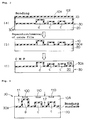
- the bonded SOI substrate according to this embodiment is characterized in that a predetermined number of shorter cavities "c" and a predetermined number of taller cavities “d” defining their heights taller than said shorter cavities "c” reside in an active layer wafer 10 side with respect to a bonding interface between an active layer 10A and a supporting substrate wafer 20.
- This difference in height results in a difference in thickness of the SOI layer (active layer) 10A in these regions.
- the SOI layer 10A having the thickness "t1" is formed above the cavity "d” and the SOI layer 10A having the thickness "t2" is formed above the cavity "c", respectively. It is to be noted that t1 ⁇ t2.
- CMOS transistor 100 will be formed in this region of the thinner silicon layer and a bipolar transistor 110 will be formed in the region of the thicker silicon layer, respectively.
- hydrogen ions are ion-implanted in accordance with a specified condition into a back surface (at a location defined by a predetermined depth from a surface of mirror-surface) of the silicon wafer 10 for the active layer having fabricated by a known method.
- Fig. 1(a) shows this ion implantation is being carried out.
- 10a indicates the region where the hydrogen ions are implanted.
- a reactive ion etching apparatus is used to form recessed portions 10d each defined by an opening area of 1 mm 2 x a depth of 0.5 ⁇ m and recessed portions 10e each defined by an opening area of 1 mm 2 x a depth of 1.0 ⁇ m with the ion etching in the surface of the active layer silicon wafer 10.
- Fig. 1(b) shows the condition after the etching.
- a plurality of types of mask is prepared for the etching, and the etching is applied in a plurality of steps.
- a silicon oxide film 10f is formed across the entire exposed surface of the active layer wafer 10 including the recessed portions 10d, 10e by the thermal oxidation processing at 900°C in the oxygen gas atmosphere.
- the surface of the active layer silicon wafer 10 i. e. , the surface having the recessed portions
- the mirror-surface of the previously prepared supporting substrate wafer 20 i.e., the silicon wafer fabricated in the same process as the active layer wafer 10
- the bonding surfaces laminating surfaces
- an insulation layer will be formed between the active layer wafer 10 and the supporting substrate wafer 20, which insulation layer comprises a predetermined number of cavities "c" each defined by the opening area of 1 mm 2 x the height of 0.5 ⁇ m, a predetermined number of cavities “d” each defined by the opening area of 1 mm 2 x the height of 1.0 ⁇ m and a buried oxide film 30a located in the bonding surface side of the silicon oxide film 10f.
- Fig. 2(a) shows a state after this bonding step.
- the heat treatment at a low temperature is applied to the bonded wafer 30 at 500°C for one hour to thereby form a hydrogen bubble region 10a within the active layer wafer 10.
- the hydrogen ions having been implanted in the above-mentioned step form the bubbles.
- the predetermined bonding heat treatment (1100°C, two hours) is applied to this bonded wafer 30.
- Fig. 2(b) shows a condition where the oxidation film has been removed after the separation.
- the bonding strength of the bonded wafer 30 is enhanced by this bonding heat treatment.
- the separation surface of the active layer wafer 10 is subjected to the CMP processing (polishing) or the hydrogen bake processing to thereby fabricate a bonded SOI substrate.
- Fig. 2(c) shows its resultant condition.
- the surface of the active layer wafer is mirror-polished through the polishing. It is to be noted that the element 30a functions as the buried oxide film.
- Fig. 3 shows the state where the elements have been formed on thus fabricated bonded SOI substrate.
- the SOI layer 10A right above the cavity “c” and that above the cavity “d” have different thickness from each other.
- the thin (thickness t1) SOI layer 10A is formed right above the taller cavity “d”
- the thick (thickness t2) SOI layer 10A is formed right above the shorter cavity "c", respectively.
- the CMOS logic is formed in the specific region of the SOI layer 10A located above the taller cavity "d", as described above. This is because the region in which the CMOS logic is formed has preferably the thin film where a parasitic capacity could be made as small as possible. Further, the memory or various types of analog circuits (bipolar elements) may be formed in the region located above the shorter cavity "c" (the thicker region) in the SOI layer 10A.
- a base circuit of the CMOS logic, a unit transistor of the other type than the CMOS logic, a channel of the unit transistor, a variety of complete depletion type SOI device and the like may be formed in the region above the cavity "d" of the SOI layer 10A.
- the elements having different structures from each other are allowed to reside in a mixed manner on the same chip.
- Fig. 4 through Fig. 6 a second embodiment of the present invention is illustrated.
- the manufacturing method of the SOI substrate according to this embodiment is characterized in that in the step prior to the hydrogen ion implantation, firstly a silicon-germanium thin film 10b is epitaxially-grown on the surface (mirror-surface) of the active layer silicon wafer 10, and secondly a silicon thin film 10c is successively epitaxially-grown on the surface of the silicon-germanium thin film 10b, as shown in Fig. 4.
- the active layer silicon wafer 10 such a silicon wafer may be employed that has been pulled up by the CZ method (Czochralski method) and processed by the slicing, beveling, lapping, etching and mirror-surface polishing.
- CZ method Czochralski method
- the hydrogen ions are implanted into the interface between this silicon-germanium (SiGe) thin film 10b and the active layer wafer 10 or into the SiGe film 10b, or otherwise into the silicon substrate immediate below the SiGe film such that the hydrogen ion concentration reaches its peak in those regions.
- Reference numeral 10a indicates the hydrogen ion implanted region. In this way, the active layer wafer 10 to be bonded is fabricated.
- the predetermined recessed portions 20a, 20b are formed in its bonding surface (mirror-surface) by the photolithography or the like, as shown in Fig. 5.
- the respective recessed portions 20a, 20b are controlled to have different depths from each other. This may be accomplished by, for example, applying different conditions of etching associated with the photo mask to the expected recessed portions 20a and 20b respectively.
- the recessed portion 20a is exclusively etched by a predetermined depth
- the recessed portions 20a and 20b are etched by a predetermined depths. That is, the recessed portion 20a is etched through two times of etching to be deeper than the recessed portion 20b, for example, as two times deeper as the recessed portion 20b.
- the outer surface of the supporting substrate wafer 20 is coated with the oxide film 20c by the thermal oxidation. It is to be noted that the supporting substrate wafer 20 has been formed through the same processes as those for said active layer wafer 10.
- those active layer wafer 10 and the supporting substrate wafer 20 are bonded to each other thus to fabricate a bonded wafer 30.
- the active layer wafer 10 and the supporting substrate wafer 20 are placed one over the other with the surface of the silicon thin film 10c of the former facing the surface (the recessed portion formed surface) of the latter, to thereby bond those two wafers to each other.
- the bonded wafer 30 is inserted into the thermal oxidation furnace to be subjected to the predetermined heat treatment. That is, under a condition defined by the oxygen gas atmosphere, the temperature of 500°C and the processing time of one hour, the hydrogen bubbles are formed in the hydrogen ion implanted region 10a.
- the bonding heat treatment is carried out at 1100°C for two hours. As a result, the bonding strength is enhanced.
- the active layer wafer 10 is separated off from the hydrogen bubble formed region (the interface between the silicon-germanium thin film 10b and the active layer wafer 10).
- the bonded wafer 30 is formed with the silicon oxide film (the buried oxide film) 30a interposed between the bonding surfaces. Then, in this case, the silicon oxide film 30a would include the cavities "a" and "b” in parts thereof (at locations spaced from each other in the same plane).
- the silicon-germanium thin film 10b is etched by using the etch stop method to remove it and thereby to expose the silicon thin film 10c.
- an etchant is used that has the etching rate for the silicon-germanium greater than that for the silicon. Further, this etching surface is polished by the chemical and mechanical polishing to be the mirror-surface.
- a bonded SOI substrate is fabricated, which has the SOI layer 10A comprising the silicon thin film 10c having the predetermined thickness.
- the predetermined elements are to be formed in the SOI layer 10A in the regions right above the respective cavities 20a and 20b.
- the separation surface is within the silicon-germanium film 10b or within the active layer silicon wafer 10 immediately below the silicon-germanium thin film 10b, and further since unnecessary layer is removed by the etching in the subsequent step, the final roughness of the surface of the SOI layer can be reduced.
- Fig. 7 through Fig. 9 a third embodiment of the present invention is illustrated.
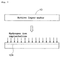
- a single crystal silicon ingot that has been pulled up by the CZ method is further processed through the slicing, beveling, lapping, etching and polishing to thereby prepare the active layer wafer 10 having a thickness of 725 ⁇ m, a diameter of 200 nm, and an initial oxygen concentration of 14.0 x 10 17 atoms/cc, with its surface having been mirror-surface finished (Fig. 7).
- hydrogen ions are implanted at a rate of 5.0 x 10 16 atoms/cm 2 into the active layer wafer 10 by using a medium current ion implanter with an accelerating voltage of 100 keV so as to achieve the depth of implantation of about 2 ⁇ m from the wafer surface side.
- the hydrogen ion implanted layer 10a is formed in the surface layer of the active wafer 10 at a predetermined depth from a surface thereof as an extending plane.
- the supporting substrate wafer 20 is prepared by the same manufacturing method as that used for the active layer wafer 10 so as to have the same thickness, diameter andmirror-surface therewith (Fig. 8).
- this supporting substrate wafer 20 is applied with a resist film by 1 ⁇ m entirely across the surface thereof by the spin coating method.
- a plurality of recessed portions 20a each defined by an opening area of 1 mm 2 x a depth of 0.5 ⁇ m and a plurality of recessed portions 20b each defined by an opening area of 1 mm 2 x a depth of 1.0 ⁇ m are formed in a part of the surface of the supporting substrate wafer 20 by the ion etching.
- this supporting substrate wafer 20 is inserted into the thermal oxidation furnace, where the wafer 20 is processed with the thermal oxidation at 900°C while supplying a flow of oxygen gas at a predetermined flow rate.
- the 0.4 ⁇ m thick insulating silicon oxide film 20c is formed entirely across the exposed surface of the supporting substrate wafer 20 including entire regions in the inner walls of the recessed portions 20a and 20b.
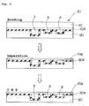
- the active layer wafer 10 and the supporting substrate wafer 20 are placed one over the other under the room temperature in the vacuum device, such that the surface of the hydrogen ion implanted layer 10a side of the active layer wafer 10 and the surface of the recessed portion 20a, 20b side of the supporting substrate wafer 20 serve as the bonding surfaces, thus to form the bonded wafer 30 (Fig. 9).
- the pressure inside of the vacuum device is kept to be equal or less than 10 Torr. Bonding the two wafer in the vacuum device allows the mirror finished surface of the active layer wafer 10 and the mirror finished surface in the recessed portion 20a, 20b side of the supporting substrate wafer 20 to be bonded to each other without generating any bad bonding regions therebetween.
- a predetermined number of cavities "a" each defined by the opening area of 1 mm 2 x the depth of 0.5 ⁇ m and a predetermined number of cavities "b" each defined by the opening area of 1 mm 2 x the depth of 1.0 ⁇ m are formed respectively.
- the portion of the silicon oxide film 20c interposed between the active layer wafer 10 and the supporting substrate wafer 20 turns out to be the buried silicon oxide film 30a.
- the thickness of this buried silicon oxide film 30a is 0.4 ⁇ m.
- this illustrated embodiment has been configured such that the bonding method is employed to manufacture the bonded SOI substrate having the cavities "a” and "b", the cavities "a” and “b” can be formed with higher dimensional precision as compared to the prior art using the migration of the silicon atoms.
- this bonded wafer 30 is inserted in the thermal oxidation furnace for the bonding heat treatment, where it is processed with the heat treatment for forming bubbles under the oxygen gas atmosphere at 500°C for one hour. This causes the hydrogen ions implanted in the active layer wafer 10 to react and thus form a region where a large number of hydrogen bubbles is generated in high density.
- the bonding heat treatment is carried out at 1100°C for two hours. This may enhance the bonding strength between the active layer wafer 10 and the supporting substrate wafer 20.
- unnecessary portions of the active layer wafer 10 is separated off from the hydrogen bubble formed region, thus to make the active layer wafer 10 thinner. Consequently, the active layer 10A having the predetermined thickness emerges on the supporting substrate wafer 20 via the insulation layer comprising the cavities "a" and "b" and the buried oxide film 30a.
- the silicon oxide film, which has been formed on the exposed surfaces of the active layer 10A and the supporting substrate wafer 20 during the heat treatment is removed by applying the HF cleaning process.
- the CMP Chemical Mechanical Polishing
- the separation surface of the active layer 10A is finished into mirror-surface.
- the hydrogen baking may be employed in place of the CMP to process the separation surface of the active layer 10A.
- the recessed portions are formed in the surface of the active layer wafer and/or in the surface of the supporting substrate wafer, and then the active layer wafer and the supporting substrate wafer are bonded to each other such that the surfaces having those recessed portions may serve as the bonding surfaces, therefore the insulation layer comprising cavities of higher dimensional precision can be formed within the substrate.
- the MOS regions and the bipolar device regions may be formed in a mixed manner.
- this bonded SOI substrate allows the elements of different structures to be formed thereon in a mixed manner.
- the respective elements are allowed to perform their functions effectively.
- respective portions of the elements are also allowed to perform their optimal functions.
- such a configuration may be employed in which each of the MOS type element and the bipolar type element can perform its function sufficiently.
Landscapes
- Element Separation (AREA)
- Thin Film Transistor (AREA)
Applications Claiming Priority (3)
| Application Number | Priority Date | Filing Date | Title |
|---|---|---|---|
| JP2002307478 | 2002-10-22 | ||
| JP2002307478A JP4556158B2 (ja) | 2002-10-22 | 2002-10-22 | 貼り合わせsoi基板の製造方法および半導体装置 |
| PCT/JP2003/013514 WO2004038790A1 (ja) | 2002-10-22 | 2003-10-22 | 貼り合わせsoi基板およびその製造方法ならびに半導体装置 |
Publications (3)
| Publication Number | Publication Date |
|---|---|
| EP1555690A1 true EP1555690A1 (de) | 2005-07-20 |
| EP1555690A4 EP1555690A4 (de) | 2006-10-04 |
| EP1555690B1 EP1555690B1 (de) | 2014-07-16 |
Family
ID=32170939
Family Applications (1)
| Application Number | Title | Priority Date | Filing Date |
|---|---|---|---|
| EP03809450.4A Expired - Lifetime EP1555690B1 (de) | 2002-10-22 | 2003-10-22 | Eingefügtes soi-substrat, prozess zu seiner herstellung und halbleiterbauelement |
Country Status (7)
| Country | Link |
|---|---|
| US (1) | US7253082B2 (de) |
| EP (1) | EP1555690B1 (de) |
| JP (1) | JP4556158B2 (de) |
| KR (1) | KR100734229B1 (de) |
| CN (1) | CN100474554C (de) |
| TW (1) | TWI233151B (de) |
| WO (1) | WO2004038790A1 (de) |
Cited By (1)
| Publication number | Priority date | Publication date | Assignee | Title |
|---|---|---|---|---|
| US8212319B2 (en) | 2007-04-25 | 2012-07-03 | Semiconductor Energy Laboratory Co., Ltd. | Semiconductor device comprising semiconductor film with recess |
Families Citing this family (48)
| Publication number | Priority date | Publication date | Assignee | Title |
|---|---|---|---|---|
| RU2217842C1 (ru) * | 2003-01-14 | 2003-11-27 | Институт физики полупроводников - Объединенного института физики полупроводников СО РАН | Способ изготовления структуры кремний-на-изоляторе |
| US7538010B2 (en) * | 2003-07-24 | 2009-05-26 | S.O.I.Tec Silicon On Insulator Technologies | Method of fabricating an epitaxially grown layer |
| FR2857983B1 (fr) * | 2003-07-24 | 2005-09-02 | Soitec Silicon On Insulator | Procede de fabrication d'une couche epitaxiee |
| KR20050051921A (ko) * | 2003-11-28 | 2005-06-02 | 학교법인 동서학원 | 매몰 캐비티를 갖는 에스오아이기판 제조방법 |
| JP2006040911A (ja) * | 2004-07-22 | 2006-02-09 | Renesas Technology Corp | 半導体装置及びその製造方法 |
| JP4559839B2 (ja) * | 2004-12-13 | 2010-10-13 | トヨタ自動車株式会社 | 半導体装置の製造方法 |
| JP5028845B2 (ja) * | 2006-04-14 | 2012-09-19 | 株式会社Sumco | 貼り合わせウェーハ及びその製造方法 |
| KR100840785B1 (ko) * | 2007-02-16 | 2008-06-23 | 삼성전자주식회사 | 스택형 반도체 소자에서 단결정 실리콘 패턴 형성 방법. |
| US7922920B2 (en) * | 2007-02-27 | 2011-04-12 | The United States Of America As Represented By The Administrator Of The National Aeronautics And Space Administration | Systems, methods, and apparatus of a low conductance silicon micro-leak for mass spectrometer inlet |
| JP5350655B2 (ja) | 2007-04-27 | 2013-11-27 | 株式会社半導体エネルギー研究所 | 半導体装置 |
| EP1993126B1 (de) * | 2007-05-18 | 2011-09-21 | Semiconductor Energy Laboratory Co., Ltd. | Verfahren zur Herstellung eines Halbleitersubstrats |
| JP2008300709A (ja) * | 2007-06-01 | 2008-12-11 | Semiconductor Energy Lab Co Ltd | 半導体装置及びその作製方法 |
| JP5190225B2 (ja) * | 2007-07-19 | 2013-04-24 | 株式会社半導体エネルギー研究所 | 半導体装置及びその作製方法 |
| FR2921749B1 (fr) * | 2007-09-27 | 2014-08-29 | Soitec Silicon On Insulator | Procede de fabrication d'une structure comprenant un substrat et une couche deposee sur l'une de ses faces. |
| JP5201967B2 (ja) * | 2007-12-10 | 2013-06-05 | 株式会社半導体エネルギー研究所 | 半導体基板の作製方法および半導体装置の作製方法 |
| FR2935536B1 (fr) * | 2008-09-02 | 2010-09-24 | Soitec Silicon On Insulator | Procede de detourage progressif |
| EP2200077B1 (de) * | 2008-12-22 | 2012-12-05 | Soitec | Verfahren zur Bindung zweier Substrate |
| FR2942911B1 (fr) * | 2009-03-09 | 2011-05-13 | Soitec Silicon On Insulator | Procede de realisation d'une heterostructure avec adaptation locale de coefficient de dilatation thermique |
| FR2961630B1 (fr) | 2010-06-22 | 2013-03-29 | Soitec Silicon On Insulator Technologies | Appareil de fabrication de dispositifs semi-conducteurs |
| US8338266B2 (en) | 2010-08-11 | 2012-12-25 | Soitec | Method for molecular adhesion bonding at low pressure |
| FR2964193A1 (fr) | 2010-08-24 | 2012-03-02 | Soitec Silicon On Insulator | Procede de mesure d'une energie d'adhesion, et substrats associes |
| US9754860B2 (en) | 2010-12-24 | 2017-09-05 | Qualcomm Incorporated | Redistribution layer contacting first wafer through second wafer |
| US9624096B2 (en) | 2010-12-24 | 2017-04-18 | Qualcomm Incorporated | Forming semiconductor structure with device layers and TRL |
| US9553013B2 (en) | 2010-12-24 | 2017-01-24 | Qualcomm Incorporated | Semiconductor structure with TRL and handle wafer cavities |
| US8536021B2 (en) | 2010-12-24 | 2013-09-17 | Io Semiconductor, Inc. | Trap rich layer formation techniques for semiconductor devices |
| US8481405B2 (en) | 2010-12-24 | 2013-07-09 | Io Semiconductor, Inc. | Trap rich layer with through-silicon-vias in semiconductor devices |
| EP3734645B1 (de) | 2010-12-24 | 2025-09-10 | Qualcomm Incorporated | Schicht mit hoher haftstellendichte für halbleiterbauelemente |
| KR20130040496A (ko) * | 2011-10-14 | 2013-04-24 | 삼성코닝정밀소재 주식회사 | 접합기판 및 이의 제조방법 |
| US8502327B1 (en) | 2012-01-26 | 2013-08-06 | Honeywell International Inc. | Systems and methods for conductive pillars |
| US9184094B1 (en) * | 2012-01-26 | 2015-11-10 | Skorpios Technologies, Inc. | Method and system for forming a membrane over a cavity |
| JP5933289B2 (ja) | 2012-02-23 | 2016-06-08 | 三菱電機株式会社 | Soiウエハおよびその製造方法 |
| WO2014181518A1 (ja) | 2013-05-09 | 2014-11-13 | 株式会社デンソー | Soi基板、物理量センサ、soi基板の製造方法、および物理量センサの製造方法 |
| CN103241708A (zh) * | 2013-05-14 | 2013-08-14 | 上海新傲科技股份有限公司 | 带有空腔的衬底的制备方法 |
| JP6061251B2 (ja) * | 2013-07-05 | 2017-01-18 | 株式会社豊田自動織機 | 半導体基板の製造方法 |
| WO2016018288A1 (en) | 2014-07-30 | 2016-02-04 | Hewlett-Packard Development Company, L.P. | Hybrid multilayer device |
| GB2532733A (en) * | 2014-11-25 | 2016-06-01 | Melexis Technologies Nv | Radiation detector comprising a compensating sensor |
| JP5817905B1 (ja) * | 2014-12-15 | 2015-11-18 | 富士ゼロックス株式会社 | 半導体片の製造方法 |
| US9466729B1 (en) | 2015-05-08 | 2016-10-11 | Qualcomm Incorporated | Etch stop region based fabrication of bonded semiconductor structures |
| US10658177B2 (en) | 2015-09-03 | 2020-05-19 | Hewlett Packard Enterprise Development Lp | Defect-free heterogeneous substrates |
| CN105226004A (zh) * | 2015-10-19 | 2016-01-06 | 上海华力微电子有限公司 | 具有应力集中结构的soi晶圆的制造方法 |
| CN105633084A (zh) * | 2015-12-29 | 2016-06-01 | 中国科学院上海微系统与信息技术研究所 | 一种基于绝缘体岛上硅衬底的cmos器件结构及制备方法 |
| WO2017123245A1 (en) * | 2016-01-15 | 2017-07-20 | Hewlett Packard Enterprise Development Lp | Multilayer device |
| WO2017171737A1 (en) | 2016-03-30 | 2017-10-05 | Hewlett Packard Enterprise Development Lp | Devices having substrates with selective airgap regions |
| CN107265399A (zh) * | 2017-07-03 | 2017-10-20 | 上海先进半导体制造股份有限公司 | 硅片密封腔体的制作方法 |
| US10381801B1 (en) | 2018-04-26 | 2019-08-13 | Hewlett Packard Enterprise Development Lp | Device including structure over airgap |
| CN108622851A (zh) * | 2018-04-28 | 2018-10-09 | 中科芯集成电路股份有限公司 | 一种带有空腔的衬底的制备方法 |
| CN111952241A (zh) * | 2020-08-21 | 2020-11-17 | 中国科学院上海微系统与信息技术研究所 | 具有辅助支撑结构的半导体衬底及其制备方法 |
| JP2024085189A (ja) * | 2022-12-14 | 2024-06-26 | タツモ株式会社 | 半導体デバイスの製造方法 |
Family Cites Families (28)
| Publication number | Priority date | Publication date | Assignee | Title |
|---|---|---|---|---|
| US3902936A (en) * | 1973-04-04 | 1975-09-02 | Motorola Inc | Germanium bonded silicon substrate and method of manufacture |
| US4260579A (en) * | 1979-05-10 | 1981-04-07 | Miles Laboratories, Inc. | Device and method for simulating bilirubin in urine |
| JPS61184843A (ja) | 1985-02-13 | 1986-08-18 | Toshiba Corp | 複合半導体装置とその製造方法 |
| US5164218A (en) * | 1989-05-12 | 1992-11-17 | Nippon Soken, Inc. | Semiconductor device and a method for producing the same |
| JPH046875A (ja) * | 1990-04-24 | 1992-01-10 | Mitsubishi Materials Corp | シリコンウェーハ |
| US5238865A (en) * | 1990-09-21 | 1993-08-24 | Nippon Steel Corporation | Process for producing laminated semiconductor substrate |
| US5091330A (en) | 1990-12-28 | 1992-02-25 | Motorola, Inc. | Method of fabricating a dielectric isolated area |
| DE4124363C2 (de) | 1991-07-23 | 1994-02-03 | Daimler Benz Ag | Verfahren zur Überwachung des Kältemittel-Füllstandes in einer Kälteanlage |
| US5346848A (en) * | 1993-06-01 | 1994-09-13 | Motorola, Inc. | Method of bonding silicon and III-V semiconductor materials |
| FR2715502B1 (fr) * | 1994-01-26 | 1996-04-05 | Commissariat Energie Atomique | Structure présentant des cavités et procédé de réalisation d'une telle structure. |
| JPH09135030A (ja) * | 1995-11-08 | 1997-05-20 | Hitachi Ltd | 半導体集積回路装置およびそれを用いたコンピュータシステム、ならびに半導体集積回路装置の製造方法 |
| FR2748851B1 (fr) * | 1996-05-15 | 1998-08-07 | Commissariat Energie Atomique | Procede de realisation d'une couche mince de materiau semiconducteur |
| DE19732237C2 (de) * | 1997-01-10 | 2003-07-17 | Nat Semiconductor Corp | Verfahren zum Bilden eines mehrschichtigen Wafers und mehrschichtiger Wafer |
| US6191007B1 (en) * | 1997-04-28 | 2001-02-20 | Denso Corporation | Method for manufacturing a semiconductor substrate |
| US5949108A (en) * | 1997-06-30 | 1999-09-07 | Intel Corporation | Semiconductor device with reduced capacitance |
| US6534380B1 (en) * | 1997-07-18 | 2003-03-18 | Denso Corporation | Semiconductor substrate and method of manufacturing the same |
| JP4144047B2 (ja) * | 1997-08-20 | 2008-09-03 | 株式会社デンソー | 半導体基板の製造方法 |
| JPH11145481A (ja) * | 1997-11-06 | 1999-05-28 | Denso Corp | 半導体基板およびその製造方法 |
| US6114197A (en) * | 1998-02-26 | 2000-09-05 | Sharp Laboratories Of America, Inc. | Method of forming fully depleted SIMOX CMOS having electrostatic discharge protection |
| JP4074051B2 (ja) | 1999-08-31 | 2008-04-09 | 株式会社東芝 | 半導体基板およびその製造方法 |
| JP3957038B2 (ja) | 2000-11-28 | 2007-08-08 | シャープ株式会社 | 半導体基板及びその作製方法 |
| EP1364398A4 (de) * | 2001-01-02 | 2011-11-30 | Draper Lab Charles S | Verfahren zur mikroherstellung von strukturen unter verwendung von silizium-auf-isolator-material |
| US6613652B2 (en) * | 2001-03-14 | 2003-09-02 | Chartered Semiconductor Manufacturing Ltd. | Method for fabricating SOI devices with option of incorporating air-gap feature for better insulation and performance |
| US6759282B2 (en) * | 2001-06-12 | 2004-07-06 | International Business Machines Corporation | Method and structure for buried circuits and devices |
| US6660564B2 (en) * | 2002-01-25 | 2003-12-09 | Sony Corporation | Wafer-level through-wafer packaging process for MEMS and MEMS package produced thereby |
| US6958255B2 (en) * | 2002-08-08 | 2005-10-25 | The Board Of Trustees Of The Leland Stanford Junior University | Micromachined ultrasonic transducers and method of fabrication |
| JP3916536B2 (ja) * | 2002-09-02 | 2007-05-16 | 沖電気工業株式会社 | Lsiデバイスの製造方法 |
| JP2004103611A (ja) * | 2002-09-04 | 2004-04-02 | Toshiba Corp | 半導体装置及びその製造方法 |
-
2002
- 2002-10-22 JP JP2002307478A patent/JP4556158B2/ja not_active Expired - Lifetime
-
2003
- 2003-10-21 TW TW092129099A patent/TWI233151B/zh not_active IP Right Cessation
- 2003-10-22 CN CNB2003801002358A patent/CN100474554C/zh not_active Expired - Lifetime
- 2003-10-22 KR KR1020047011567A patent/KR100734229B1/ko not_active Expired - Lifetime
- 2003-10-22 WO PCT/JP2003/013514 patent/WO2004038790A1/ja not_active Ceased
- 2003-10-22 EP EP03809450.4A patent/EP1555690B1/de not_active Expired - Lifetime
- 2003-10-22 US US10/501,522 patent/US7253082B2/en not_active Expired - Lifetime
Cited By (1)
| Publication number | Priority date | Publication date | Assignee | Title |
|---|---|---|---|---|
| US8212319B2 (en) | 2007-04-25 | 2012-07-03 | Semiconductor Energy Laboratory Co., Ltd. | Semiconductor device comprising semiconductor film with recess |
Also Published As
| Publication number | Publication date |
|---|---|
| EP1555690B1 (de) | 2014-07-16 |
| US7253082B2 (en) | 2007-08-07 |
| CN1692488A (zh) | 2005-11-02 |
| EP1555690A4 (de) | 2006-10-04 |
| TWI233151B (en) | 2005-05-21 |
| CN100474554C (zh) | 2009-04-01 |
| WO2004038790A1 (ja) | 2004-05-06 |
| JP4556158B2 (ja) | 2010-10-06 |
| KR20050053525A (ko) | 2005-06-08 |
| KR100734229B1 (ko) | 2007-07-02 |
| US20050081958A1 (en) | 2005-04-21 |
| TW200409200A (en) | 2004-06-01 |
| JP2004146461A (ja) | 2004-05-20 |
Similar Documents
| Publication | Publication Date | Title |
|---|---|---|
| US7253082B2 (en) | Pasted SOI substrate, process for producing the same and semiconductor device | |
| JP2001196566A (ja) | 半導体基板およびその製造方法 | |
| EP1026729A2 (de) | Verbundbauteil und zugehöriges Trennverfahren, Stapel aus gebondeten Substraten und zugehöriges Trennverfahren, Transferverfahren für Transferschicht, und Herstellungsverfahren für ein SOI Substrat | |
| US4968628A (en) | Method of fabricating back diffused bonded oxide substrates | |
| US5420064A (en) | Method of manufacturing a dielectric isolation substrate | |
| US7067387B2 (en) | Method of manufacturing dielectric isolated silicon structure | |
| JP3120275B2 (ja) | Soi基板の製造方法 | |
| JP2976929B2 (ja) | 半導体装置の製造方法 | |
| JPH1174209A (ja) | 半導体基板の製造方法 | |
| KR100529633B1 (ko) | 에피택셜 실리콘을 이용한 반도체 소자 및 그 제조 방법 | |
| US6239469B1 (en) | Method for fabrication of silicon on insulator substrates | |
| US6153488A (en) | Method for producing semiconductor device, and semiconductor device produced by same | |
| KR100498446B1 (ko) | Soi웨이퍼 및 그의 제조방법 | |
| JP2004096044A (ja) | 基板及びその製造方法 | |
| JP2000196048A (ja) | Soiウェ―ハの製造方法 | |
| JP2005079109A (ja) | 貼合せsoiウェーハの製造方法及び該方法により製造された貼合せsoiウェーハ | |
| JP2001053257A (ja) | 張り合わせsoi基板の作製方法 | |
| KR100286776B1 (ko) | 실리콘 온 인슐레이터 웨이퍼의 제조방법 | |
| KR100312981B1 (ko) | 본딩형실리콘이중막웨이퍼제조방법 | |
| KR100286772B1 (ko) | 실리콘 온 인슐레이터 웨이퍼의 제조방법 | |
| JPH1050824A (ja) | Soi基板の製造方法 | |
| KR20000040424A (ko) | 실리콘 온 인슐레이터 웨이퍼의 제조방법 | |
| KR20000021846A (ko) | 반도체 기판 제조방법 | |
| JP2003007816A (ja) | 半導体素子の製造方法 | |
| EP0732737A2 (de) | Verbundhalbleitersubstrat und Verfahren zur Herstellung |
Legal Events
| Date | Code | Title | Description |
|---|---|---|---|
| PUAI | Public reference made under article 153(3) epc to a published international application that has entered the european phase |
Free format text: ORIGINAL CODE: 0009012 |
|
| 17P | Request for examination filed |
Effective date: 20040701 |
|
| AK | Designated contracting states |
Kind code of ref document: A1 Designated state(s): AT BE BG CH CY CZ DE DK EE ES FI FR GB GR HU IE IT LI LU MC NL PT RO SE SI SK TR |
|
| RBV | Designated contracting states (corrected) |
Designated state(s): DE FR IT |
|
| RAP1 | Party data changed (applicant data changed or rights of an application transferred) |
Owner name: SUMCO CORPORATION |
|
| A4 | Supplementary search report drawn up and despatched |
Effective date: 20060906 |
|
| 17Q | First examination report despatched |
Effective date: 20080311 |
|
| REG | Reference to a national code |
Ref country code: DE Ref legal event code: R079 Ref document number: 60346505 Country of ref document: DE Free format text: PREVIOUS MAIN CLASS: H01L0021760000 Ipc: H01L0021762000 |
|
| RIC1 | Information provided on ipc code assigned before grant |
Ipc: H01L 21/764 20060101ALI20130812BHEP Ipc: H01L 21/762 20060101AFI20130812BHEP |
|
| GRAP | Despatch of communication of intention to grant a patent |
Free format text: ORIGINAL CODE: EPIDOSNIGR1 |
|
| INTG | Intention to grant announced |
Effective date: 20131111 |
|
| GRAP | Despatch of communication of intention to grant a patent |
Free format text: ORIGINAL CODE: EPIDOSNIGR1 |
|
| INTG | Intention to grant announced |
Effective date: 20140320 |
|
| GRAS | Grant fee paid |
Free format text: ORIGINAL CODE: EPIDOSNIGR3 |
|
| GRAA | (expected) grant |
Free format text: ORIGINAL CODE: 0009210 |
|
| AK | Designated contracting states |
Kind code of ref document: B1 Designated state(s): DE FR IT |
|
| REG | Reference to a national code |
Ref country code: DE Ref legal event code: R096 Ref document number: 60346505 Country of ref document: DE Effective date: 20140828 |
|
| REG | Reference to a national code |
Ref country code: DE Ref legal event code: R097 Ref document number: 60346505 Country of ref document: DE |
|
| PG25 | Lapsed in a contracting state [announced via postgrant information from national office to epo] |
Ref country code: IT Free format text: LAPSE BECAUSE OF FAILURE TO SUBMIT A TRANSLATION OF THE DESCRIPTION OR TO PAY THE FEE WITHIN THE PRESCRIBED TIME-LIMIT Effective date: 20140716 |
|
| PLBE | No opposition filed within time limit |
Free format text: ORIGINAL CODE: 0009261 |
|
| STAA | Information on the status of an ep patent application or granted ep patent |
Free format text: STATUS: NO OPPOSITION FILED WITHIN TIME LIMIT |
|
| 26N | No opposition filed |
Effective date: 20150417 |
|
| REG | Reference to a national code |
Ref country code: FR Ref legal event code: PLFP Year of fee payment: 13 |
|
| REG | Reference to a national code |
Ref country code: FR Ref legal event code: PLFP Year of fee payment: 14 |
|
| REG | Reference to a national code |
Ref country code: DE Ref legal event code: R082 Ref document number: 60346505 Country of ref document: DE Representative=s name: GLAWE DELFS MOLL PARTNERSCHAFT MBB VON PATENT-, DE |
|
| REG | Reference to a national code |
Ref country code: FR Ref legal event code: PLFP Year of fee payment: 15 |
|
| REG | Reference to a national code |
Ref country code: FR Ref legal event code: PLFP Year of fee payment: 16 |
|
| PGFP | Annual fee paid to national office [announced via postgrant information from national office to epo] |
Ref country code: FR Payment date: 20221028 Year of fee payment: 20 |
|
| PGFP | Annual fee paid to national office [announced via postgrant information from national office to epo] |
Ref country code: DE Payment date: 20221019 Year of fee payment: 20 |
|
| REG | Reference to a national code |
Ref country code: DE Ref legal event code: R071 Ref document number: 60346505 Country of ref document: DE |