EP1307928B1 - Puce de semi-conducteur pour optoelectronique et son procede de fabrication - Google Patents
Puce de semi-conducteur pour optoelectronique et son procede de fabrication Download PDFInfo
- Publication number
- EP1307928B1 EP1307928B1 EP01984505.6A EP01984505A EP1307928B1 EP 1307928 B1 EP1307928 B1 EP 1307928B1 EP 01984505 A EP01984505 A EP 01984505A EP 1307928 B1 EP1307928 B1 EP 1307928B1
- Authority
- EP
- European Patent Office
- Prior art keywords
- layer
- semiconductor chip
- thin
- chip according
- mesas
- Prior art date
- Legal status (The legal status is an assumption and is not a legal conclusion. Google has not performed a legal analysis and makes no representation as to the accuracy of the status listed.)
- Expired - Lifetime
Links
- 239000004065 semiconductor Substances 0.000 title claims description 127
- 230000005693 optoelectronics Effects 0.000 title claims description 4
- 238000004519 manufacturing process Methods 0.000 title description 10
- 239000010409 thin film Substances 0.000 claims description 97
- 239000000758 substrate Substances 0.000 claims description 81
- 238000000034 method Methods 0.000 claims description 24
- 230000003287 optical effect Effects 0.000 claims description 10
- 238000001465 metallisation Methods 0.000 claims description 8
- AMGQUBHHOARCQH-UHFFFAOYSA-N indium;oxotin Chemical compound [In].[Sn]=O AMGQUBHHOARCQH-UHFFFAOYSA-N 0.000 claims description 3
- 229910052581 Si3N4 Inorganic materials 0.000 claims description 2
- HQVNEWCFYHHQES-UHFFFAOYSA-N silicon nitride Chemical compound N12[Si]34N5[Si]62N3[Si]51N64 HQVNEWCFYHHQES-UHFFFAOYSA-N 0.000 claims description 2
- 239000002131 composite material Substances 0.000 claims 3
- 239000010410 layer Substances 0.000 description 221
- 241000152158 Mesene Species 0.000 description 24
- 238000002310 reflectometry Methods 0.000 description 24
- 238000010586 diagram Methods 0.000 description 15
- 239000000463 material Substances 0.000 description 12
- 230000008878 coupling Effects 0.000 description 11
- 238000010168 coupling process Methods 0.000 description 11
- 238000005859 coupling reaction Methods 0.000 description 11
- 238000011835 investigation Methods 0.000 description 9
- 230000000694 effects Effects 0.000 description 7
- 238000005496 tempering Methods 0.000 description 7
- 230000008901 benefit Effects 0.000 description 6
- 238000000605 extraction Methods 0.000 description 5
- 230000005855 radiation Effects 0.000 description 5
- 230000007423 decrease Effects 0.000 description 4
- 230000008569 process Effects 0.000 description 4
- 238000000926 separation method Methods 0.000 description 4
- 238000005520 cutting process Methods 0.000 description 3
- 238000009792 diffusion process Methods 0.000 description 3
- 238000005530 etching Methods 0.000 description 3
- 239000010931 gold Substances 0.000 description 3
- 229910052751 metal Inorganic materials 0.000 description 3
- 239000002184 metal Substances 0.000 description 3
- 239000000203 mixture Substances 0.000 description 3
- 239000011347 resin Substances 0.000 description 3
- 229920005989 resin Polymers 0.000 description 3
- 229910001218 Gallium arsenide Inorganic materials 0.000 description 2
- 238000010521 absorption reaction Methods 0.000 description 2
- 229910052782 aluminium Inorganic materials 0.000 description 2
- 230000004888 barrier function Effects 0.000 description 2
- 230000005496 eutectics Effects 0.000 description 2
- 229910052737 gold Inorganic materials 0.000 description 2
- 230000006872 improvement Effects 0.000 description 2
- 230000000737 periodic effect Effects 0.000 description 2
- 238000004064 recycling Methods 0.000 description 2
- 229910052709 silver Inorganic materials 0.000 description 2
- 230000035882 stress Effects 0.000 description 2
- 238000003631 wet chemical etching Methods 0.000 description 2
- 238000001039 wet etching Methods 0.000 description 2
- 229910017401 Au—Ge Inorganic materials 0.000 description 1
- 229910000530 Gallium indium arsenide Inorganic materials 0.000 description 1
- VYPSYNLAJGMNEJ-UHFFFAOYSA-N Silicium dioxide Chemical compound O=[Si]=O VYPSYNLAJGMNEJ-UHFFFAOYSA-N 0.000 description 1
- 239000000853 adhesive Substances 0.000 description 1
- 230000001070 adhesive effect Effects 0.000 description 1
- 230000032683 aging Effects 0.000 description 1
- 229910045601 alloy Inorganic materials 0.000 description 1
- 239000000956 alloy Substances 0.000 description 1
- 238000005275 alloying Methods 0.000 description 1
- 238000013459 approach Methods 0.000 description 1
- 230000015572 biosynthetic process Effects 0.000 description 1
- 238000007664 blowing Methods 0.000 description 1
- 238000005266 casting Methods 0.000 description 1
- 239000002800 charge carrier Substances 0.000 description 1
- 238000003486 chemical etching Methods 0.000 description 1
- 238000005253 cladding Methods 0.000 description 1
- 239000011247 coating layer Substances 0.000 description 1
- 239000004020 conductor Substances 0.000 description 1
- 230000001419 dependent effect Effects 0.000 description 1
- 238000000151 deposition Methods 0.000 description 1
- 238000013461 design Methods 0.000 description 1
- 238000010292 electrical insulation Methods 0.000 description 1
- 230000002349 favourable effect Effects 0.000 description 1
- 239000010408 film Substances 0.000 description 1
- PCHJSUWPFVWCPO-UHFFFAOYSA-N gold Chemical compound [Au] PCHJSUWPFVWCPO-UHFFFAOYSA-N 0.000 description 1
- 238000000227 grinding Methods 0.000 description 1
- 230000001404 mediated effect Effects 0.000 description 1
- 150000002739 metals Chemical class 0.000 description 1
- 238000002161 passivation Methods 0.000 description 1
- 230000008092 positive effect Effects 0.000 description 1
- 238000003825 pressing Methods 0.000 description 1
- 238000012545 processing Methods 0.000 description 1
- 230000006798 recombination Effects 0.000 description 1
- 238000005215 recombination Methods 0.000 description 1
- 229910052814 silicon oxide Inorganic materials 0.000 description 1
- 229910000679 solder Inorganic materials 0.000 description 1
- 238000003892 spreading Methods 0.000 description 1
- 230000007480 spreading Effects 0.000 description 1
- 230000006641 stabilisation Effects 0.000 description 1
- 238000011105 stabilization Methods 0.000 description 1
- 230000007704 transition Effects 0.000 description 1
Images


Classifications
-
- H—ELECTRICITY
- H01—ELECTRIC ELEMENTS
- H01L—SEMICONDUCTOR DEVICES NOT COVERED BY CLASS H10
- H01L33/00—Semiconductor devices having potential barriers specially adapted for light emission; Processes or apparatus specially adapted for the manufacture or treatment thereof or of parts thereof; Details thereof
- H01L33/02—Semiconductor devices having potential barriers specially adapted for light emission; Processes or apparatus specially adapted for the manufacture or treatment thereof or of parts thereof; Details thereof characterised by the semiconductor bodies
- H01L33/20—Semiconductor devices having potential barriers specially adapted for light emission; Processes or apparatus specially adapted for the manufacture or treatment thereof or of parts thereof; Details thereof characterised by the semiconductor bodies with a particular shape, e.g. curved or truncated substrate
-
- H—ELECTRICITY
- H01—ELECTRIC ELEMENTS
- H01L—SEMICONDUCTOR DEVICES NOT COVERED BY CLASS H10
- H01L33/00—Semiconductor devices having potential barriers specially adapted for light emission; Processes or apparatus specially adapted for the manufacture or treatment thereof or of parts thereof; Details thereof
- H01L33/005—Processes
- H01L33/0093—Wafer bonding; Removal of the growth substrate
-
- H—ELECTRICITY
- H01—ELECTRIC ELEMENTS
- H01L—SEMICONDUCTOR DEVICES NOT COVERED BY CLASS H10
- H01L33/00—Semiconductor devices having potential barriers specially adapted for light emission; Processes or apparatus specially adapted for the manufacture or treatment thereof or of parts thereof; Details thereof
- H01L33/02—Semiconductor devices having potential barriers specially adapted for light emission; Processes or apparatus specially adapted for the manufacture or treatment thereof or of parts thereof; Details thereof characterised by the semiconductor bodies
- H01L33/08—Semiconductor devices having potential barriers specially adapted for light emission; Processes or apparatus specially adapted for the manufacture or treatment thereof or of parts thereof; Details thereof characterised by the semiconductor bodies with a plurality of light emitting regions, e.g. laterally discontinuous light emitting layer or photoluminescent region integrated within the semiconductor body
-
- H—ELECTRICITY
- H01—ELECTRIC ELEMENTS
- H01L—SEMICONDUCTOR DEVICES NOT COVERED BY CLASS H10
- H01L33/00—Semiconductor devices having potential barriers specially adapted for light emission; Processes or apparatus specially adapted for the manufacture or treatment thereof or of parts thereof; Details thereof
- H01L33/02—Semiconductor devices having potential barriers specially adapted for light emission; Processes or apparatus specially adapted for the manufacture or treatment thereof or of parts thereof; Details thereof characterised by the semiconductor bodies
- H01L33/10—Semiconductor devices having potential barriers specially adapted for light emission; Processes or apparatus specially adapted for the manufacture or treatment thereof or of parts thereof; Details thereof characterised by the semiconductor bodies with a light reflecting structure, e.g. semiconductor Bragg reflector
-
- H—ELECTRICITY
- H01—ELECTRIC ELEMENTS
- H01L—SEMICONDUCTOR DEVICES NOT COVERED BY CLASS H10
- H01L2924/00—Indexing scheme for arrangements or methods for connecting or disconnecting semiconductor or solid-state bodies as covered by H01L24/00
- H01L2924/0001—Technical content checked by a classifier
- H01L2924/0002—Not covered by any one of groups H01L24/00, H01L24/00 and H01L2224/00
-
- H—ELECTRICITY
- H01—ELECTRIC ELEMENTS
- H01L—SEMICONDUCTOR DEVICES NOT COVERED BY CLASS H10
- H01L33/00—Semiconductor devices having potential barriers specially adapted for light emission; Processes or apparatus specially adapted for the manufacture or treatment thereof or of parts thereof; Details thereof
- H01L33/02—Semiconductor devices having potential barriers specially adapted for light emission; Processes or apparatus specially adapted for the manufacture or treatment thereof or of parts thereof; Details thereof characterised by the semiconductor bodies
- H01L33/26—Materials of the light emitting region
- H01L33/30—Materials of the light emitting region containing only elements of Group III and Group V of the Periodic Table
-
- H—ELECTRICITY
- H01—ELECTRIC ELEMENTS
- H01L—SEMICONDUCTOR DEVICES NOT COVERED BY CLASS H10
- H01L33/00—Semiconductor devices having potential barriers specially adapted for light emission; Processes or apparatus specially adapted for the manufacture or treatment thereof or of parts thereof; Details thereof
- H01L33/36—Semiconductor devices having potential barriers specially adapted for light emission; Processes or apparatus specially adapted for the manufacture or treatment thereof or of parts thereof; Details thereof characterised by the electrodes
- H01L33/40—Materials therefor
- H01L33/405—Reflective materials
Definitions
- the carrier substrate is part of the semiconductor chip per se and mechanical support for the thin film layer, i. H. the essential supporting element for the thin-film layer, which no longer has a self-supporting layer even on the side opposite the carrier substrate.
- a thin-film layer based on In 1-xy Al x Ga y P means that the thin-film layer has a plurality of layers made of doped or Undoped material from the system In 1-xy Al x Ga y P (where 0 ⁇ x ⁇ 1, 0 ⁇ y ⁇ 1 and x + y ⁇ 1) are made.
- Semiconductor chips of the type mentioned are from the US 5,008,718 and US 5,367,580 known.
- an active semiconductor layer sequence is usually applied to a substrate by an epitaxial process.
- a carrier substrate is attached to the upper side of the active semiconductor layer sequence.
- the substrate on which the semiconductor layer sequence has been deposited is at least partially removed.
- a metallic reflection layer is located between the carrier substrate and the active semiconductor layer sequence, so that no light is absorbed by the carrier substrate.
- the metallic reflection layer arranged between the carrier substrate and the active semiconductor layer sequence generally has no satisfactory reflectivity at short wavelengths.
- gold becomes increasingly inefficient as a metallic reflection layer, since the reflectivity decreases significantly.
- the elements Al and Ag can be used whose reflectivity remains relatively constant at wavelengths less than 600 nm.
- a truncated pyramidal semiconductor chip which has an active, light-emitting zone between an upper window layer and a lower window layer.
- the upper window layer and the lower window layer together form a truncated pyramid-shaped base body.
- the oblique orientation of the side walls of the window layers causes the outgoing of the active zone light is totally reflected at the side surfaces and incident almost at right angles to serving as a luminous surface base surface of the truncated pyramidal base body.
- part of the light emitted by the active zone enters the surface within the outlet cone of the semiconductor element.
- exit cone is here and shall be understood in the following the cone, which is formed of light rays whose angle of incidence on the exit surface is smaller than the critical angle for total reflection and therefore not totally reflected but are coupled directly from the semiconductor material.
- the opening angle of the exit cone is therefore twice as large as the critical angle of total reflection. Those light rays that run outside the exit cone, ie hit the exit surface at a larger angle than the critical angle of total reflection, are totally reflected.
- this concept requires a minimum thickness for the upper and lower window layer.
- the thickness of the upper and lower window layer is at least 50.8 ⁇ m (2 mils). Such a layer thickness is still in the range of feasible.
- the performance of the known semiconductor chip is to be increased, it is necessary to scale all dimensions. This results in layer thicknesses that can be produced epitaxially only at great expense. This known semiconductor chip is therefore scalable if at all then only with great technical effort.
- a method for producing a light-emitting diode in which a growth substrate is provided with holes, so that they are filled with growth of a light-emitting diode layer sequence with semiconductor material of the layer sequence.
- the semiconductor material filled in the holes of the growth substrate forms convex parts of the light-emitting diode layer sequence, which are in direct contact with the growth substrate.
- a semiconductor light-emitting device in which on the side of a Semiconductor layer sequence containing a pn junction, two mesenches are formed. On one of these mesenes a p-electrode and on the other of the mesen an n-electrode for electrically contacting the device is formed. The trench between the mesenes is formed so deep that it extends to the growth substrate of the semiconductor device.
- a solid-state display which comprises a light-emitting semiconductor body.
- a plurality of mesenches are formed in the half-conductor body on a side opposite to a growth substrate such that the pn junction of the semiconductor body is severed and the mesences extend to the growth substrate.
- the transition between an n-type region and a p-type region is formed as an ohmic interface, so that the growth substrate can be electrically conductively contacted via this mesa.
- EP0977063 discloses a female connector for opto-electronic connection. Based on this prior art, the present invention seeks to provide a producible in thin film semiconductor chip with improved light extraction and to provide a method for its production.
- Preferred embodiments and methods for producing the semiconductor chip are the subject of the subclaims.
- the cross-section of the cavity decreases from outside to inside, ie from the boundary to the carrier substrate towards the interior of the thin-film layer, and the depth of the cavity is more than half the thickness of the thin-film layer.
- the cavity or the plurality of mesences produced by the latter advantageously has the effect that the thin-film layer has contact surfaces on its connection side toward the carrier substrate, which surfaces have a small surface area relative to the overall cross-sectional area of the chip.
- This has the advantage that a comparatively large local pressure can be generated in the region of these reduced pressing surfaces - this is conducive to a secure connection between carrier substrate and thin-film layer - and at the same time, the pressure on the thin-film layer can be kept sufficiently low in order to achieve this Risk of damage to the thin film layer when connecting to the carrier substrate as far as possible excluded.
- the available bonding area is increased due to the cavity, which can also lead to the improvement of the connection between the carrier substrate and the thin film layer.
- the cavity is available for receiving excess adhesive or solder material, which makes their dosage advantageously less critical.
- the cavity also advantageously provides side surfaces at which part of the radiation emitted by the active zone is deflected so that it impinges on the exit surface of the active thin film layer facing away from the carrier substrate within the exit cone.
- the reflection occurs at the side surfaces of the active thin film layer At least in part, mesenches the reflection on a continuous planar reflective layer.
- the side surfaces protrude as deeply as possible into the thin-film layer, so that the largest possible portion of the radiation emitted by the active zone, which does not impinge directly on the exit surface and is coupled out there, is reflected (possibly even several times), that is is deflected so that it meets with an angle on the exit surface, which lies within the exit cone.
- the cavity is so deep that the active zone of the active thin film layer is severed therefrom.
- the reflection at the boundary surfaces of the mesenes causes most of the photons emitted by the active zone to strike the exit surface within the exit cone and leave the semiconductor chip.
- the thin-film layer is formed so that at least one trajectory of the photons emitted by the active zone leads from the respective mesa to one of the adjacent mesenes.
- photons that have not been reflected at one of the side surfaces of the original mesa may enter one of the adjacent mesenes and be reflected there at the side surfaces of the respective mesa so as to strike the exit surface within the exit cone.
- the mesenes are equipped with concave side surfaces.
- rays which are initially reflected at the exit surface are progressively steeper toward the exit surface with each further reflection on a side surface of a mesa, so that they eventually strike the exit surface within the exit cone.
- the mesenes are covered with a reflective layer.
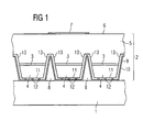
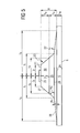
- the illustrated semiconductor chip for a light-emitting diode has a carrier substrate 1 on which the active thin-film layer 2 is mounted.
- the active thin-film layer 2 has a photon-emitting active zone 3, which is in each case formed at an average height in mesen. 4.
- the mesenes 4 may be formed like a truncated pyramid or truncated cone.
- the semiconductor chip thus constitutes a light-emitting diode.
- the mesenches 4 are arranged on a cover layer 5, which has on a flat front side 6 a central front-side contact point 7, which is preferably formed by a metallization layer.
- the backside mesenches 4 formed by cavities 8 are covered with a reflective layer consisting of a dielectric insulating layer 9 and a metallization layer 10 applied thereon.
- the insulating layer 9 is interrupted along a base surface 11 of the mesenes 4 by plated-through holes 12, which are formed by metallized sections.
- the insulating layer 9 preferably has a smaller refractive index than the adjacent semiconductor layer of the thin film layer 2. It is further formed as a diffusion barrier for the metallization layer 10. Instead of the insulating layer 9, an electrically conductive layer may also be used. Decisive are the optical properties of this layer.
- the active thin film layer 2 is first epitaxially grown on a growth substrate.
- the active thin-film layer 2 can for example be produced on the basis of InGaAlP.
- the cover layer 5 is formed on the growth substrate and then doped with a concentration above 10 18 cm -3 in order to ensure good conductivity of the cover layer 5. Because a good conductivity of the cover layer 5 is a prerequisite for the fact that on the front side 6 of the LED chip a central contact point 7 for the supply of the active zone 3 of a plurality of meseneses 4 with current suffices.
- the composition of the cover layer 5 is chosen so that it is transparent to the photons generated in the active zone. This can usually be accomplished by adjusting the band gap through the composition of the material of the cover layer 5.
- the meseneses 4 are formed with suitable wet or dry chemical etching methods. Such etching methods are known and are not the subject of the application.
- the meseneses 4 are preferably formed only in the areas provided for the semiconductor chips and there again preferably only in the areas in which light extraction can take place, that is not under contact layers 7, 43 and 49 on the upper side of the thin film layer 2.
- the provided for the semiconductor chips Areas have typical lateral outer dimensions of, for example, 400 x 400 ⁇ m 2 .
- the meseneses 4 have external dimensions which lie in the region of the layer thickness of the active thin-film layer 2. The outer dimensions of the Mesen 4 are therefore in the range of 10 microns.
- the insulating layer 9 is deposited on the meseneses 4 and the vias 12 are formed. Thereafter, the metallization layer 10 is applied.
- the active thin film layer 2 is separated according to the intended number of semiconductor chips. This is done for example by wet etching.
- the separated active thin film layers 2 are fixed to the support substrate 1 by, for example, eutectic bonding, and the growth substrate is removed by wet etching. Finally, the contact points 7 are formed on the exposed front side of the active thin-film layer 2 and the semiconductor chips are separated by separating the carrier substrate 1.
- the illustrated semiconductor chip has the advantage that the photons generated by the active zone 3 do not strike components of the semiconductor chip that absorb them. Because of the metallization layer 10, the photons are kept away from the carrier substrate 1.
- the carrier substrate can therefore advantageously be optimized very well with regard to electrical and / or thermal conductivity and / or thermal expansion.
- a further advantage is that, in the semiconductor chip of FIG. 1, a majority of the photons emitted by the active zone 3 is totally reflected on side faces 13 of the meseneses 4. The total reflected on the side surfaces 13 photons strike the front 6 at a large angle. In particular, a portion of the photons, which would be totally reflected without reflection on the side surfaces 13 on the front side, hits the front side 6 within the exit cone and can therefore leave the semiconductor chip.
- the semiconductor chip according to FIG. 1 Therefore, the reflection on the known from the prior art continuous base surface is at least partially replaced by the total reflection at the side surfaces 13. Therefore, the semiconductor chip is turned off FIG. 1 Compared to conventional semiconductor chips without cavities 8 a nearly by a factor of 2 increased light output.
- light rays should not be understood as a limitation to a particular wavelength, but as a reference to the methods of geometric optics, regardless of the wavelength.
- the meseneses 4 are designed in the shape of a truncated pyramid and are fastened to the base substrate 11 of the mesenes via a contact layer 14 on the carrier substrate 1. Through the contact layer 14, the active zone 3 is supplied with power.
- the light beams emanating from the active zone 3 are directed in the direction of the front side 6.
- the mesenes 4 cause the incident on the side surfaces 13 light beams are deflected in the direction of the front side 6 and impinge there within the exit cone, so that they can leave the semiconductor chip.
- the light output can be optimized by a suitable choice of the dimensions of the base 11, the angle of inclination of the side surface 13 and the height of the mesen as well as the position of the active zone 3.
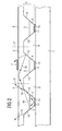
- FIG. 2 a light beam 15 is shown, which is first totally reflected on the side surface 13 and directed from there to the front 6.
- the light beam 15 strikes the interface within the exit cone and can therefore leave the semiconductor chip. Without the total reflection on the side surface 13, the light beam 15 would have been totally reflected at the front side 6 and would have been redirected to one of the reflection layers known from the prior art, where it would have been reflected again.
- the reflection on the conventional continuous reflection layer replaced by the reflection on the side surfaces 13.
- a further advantage is that the mesenes 4 are optically coupled via the cover layer 5.
- optical coupling is to be understood as meaning that at least one of the light beams emanating from the active thin-film layer 2 can pass over a center line 17 from the region of one of the mesenes 4 into the region of one of the adjacent mesenes. Because of the optical coupling with the aid of the cover layer 5, a light beam 18, which does not strike one of the side surfaces 13 of the respective mesenes 4, meet one of the side surfaces 13 of one of the adjacent mesenes 4 and be directed there to the front 6, where it is inside of the exit cone impinges. Due to the optical coupling via the cover layer 5, therefore, the light output is further increased.
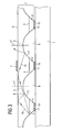
- FIG. 3 a cross section through a modified embodiment of the semiconductor chip is shown, in which the mesenes 4 are frusto-conical with concave side surfaces 13 are formed.
- the design of the side surfaces 13 results in that a light beam 18 reflected back and forth between the front side 6 and the side surface 13 is increasingly deflected toward the front side as it approaches the center line 17 until it impinges on the front side 6 within the exit cone.
- light rays 19 which first pass over the cover layer 5 from one mesa 4 to the adjacent mesa 4 and are brought there at a large angle to the front side 6.
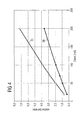
- FIG. 4 Finally, a diagram is shown in which a trace 20 represents the dependence of the luminous efficacy in relative units of the operating current in pulsed operation for a conventional, manufactured in thin film light emitting diode.
- a further measuring curve 21 illustrates the dependence of the luminous efficacy in relative units as a function of the operating current for a light-emitting diode according to the in FIG FIG. 3 illustrated embodiment.
- FIG. 4 It can be seen that the light output at the in FIG. 3 illustrated embodiments, approximately twice the luminous efficacy of conventional semiconductor chips without cavities 8 has.
- FIG. 5 a cross-sectional profile of one of the meseneses 4 is shown.
- the mesa 4 is composed of a lower truncated cone 22 and an upper truncated cone 23.
- the lower truncated cone 22 adjoins the cover layer 5 with a base surface 24.
- the active zone 3 is formed in the upper truncated cone 23, the active zone 3 is formed. It is also in FIG. 5 a arranged on the base 11 of the mesa 3 contact point 25 is provided.
- the side surfaces 13 of the mesa 4 are composed of an edge 26 of the lower truncated cone 22 and flanks 27 of the upper truncated cone 23 together.
- the geometric dimensions of the lower truncated cone 22 along a common boundary surface 28 are selected so that the flank 26 merges directly into the flank 27.
- the radius of the base surface 24 of the lower truncated cone 22 is denoted by r n , the radius of the interface 28 with r t and the radius of the base 11 with r p .
- the mesa 4 may be divided into a lower confinement layer 29 between the base surface 24 and the active zone 3 and an upper confinement layer 30 between the active zone 3 and the base 11.
- the lower boundary layer 29 has a height h u and the upper boundary layer 30 has a height h o .
- the entire height of the mesa 4 is finally denoted by H. It was consistently set at 6 ⁇ m in all examinations. For the thickness h w of the cover layer 5, a value of 2 ⁇ m was chosen in all investigations in which the thickness h w was not varied.
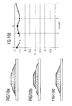
- FIGS. 6a to 6d the result of an calculation is shown, in which the radius r p of the base area 11 is set equal to 5 ⁇ m and the radius r n of the base area 24 is set equal to 20 ⁇ m .
- the radius r t of the interface 28 was between 6 and 18 ⁇ m, corresponding to the in FIG. 6a to FIG. 6c varies cross-sectional profiles varies.
- a refractive index of 3.2 was used for the active zone 3.
- the refractive index of the lower confinement layer 29, the upper confinement layer 30 and the cover layer 5 was equal to 3.3.
- the reflectivity of pad 25 was 0.3.
- the reflectivity of the base area 11 not covered by the contact point 25 and of the flanks 26 and 27 was set to the value 0.8. By reflectivity is meant in each case the energy-related reflection coefficient.
- the self-absorption of the active zone 3 by an absorption coefficient of 10,000 / cm was considered. All investigations were carried out with photon recycling. For this an internal quantum efficiency of 0.8 was assumed. The quantum efficiency in the generation of photons by charge carrier recombination was not considered.
- the decoupling efficiency ⁇ indicated in the diagrams is therefore equal to the ratio of the photons decoupled from the semiconductor chip to the number of photons actually generated. The values for the specified coupling-out efficiency ⁇ would therefore have to be multiplied by a factor of 0.8 in order to arrive at the external efficiency.
- FIG. 6c shows a diagram in which the decoupling efficiency ⁇ is plotted against the radius r t in a curve 31.
- the coupling-out efficiency of a normal thin-film semiconductor chip is shown, in which the scattering is mediated only by the photon recycling.
- This thin-film semiconductor chip with the edge length 300 ⁇ m has the same epitaxial structure as the mesa 4 in the lower truncated cone 22 and upper truncated cone 23. It was assumed, that the semiconductor chip is provided on the p-side with a mirror whose reflectivity is 0.72.
- This value is the average value of the reflectivity of a reflection layer and a contact layer weighted with the degree of occupation, the value 0.8 being used for the reflectivity of the reflection layer and 0.85 for the occupation level of the reflection layer and the value 0 for the reflectivity of the contact layer. 3 and the occupancy rate 0.15 was used.
- FIG. 6 can be seen that at a very large angle ⁇ o of the upper truncated cone 23 according to the in FIG. 6a Cross-sectional profile shown the coupling-out efficiency ⁇ is hardly better than the coupling-out efficiency ⁇ of a conventional thin-film light emitting diode whose coupling-out efficiency in FIG. 6d is shown by the straight line 32.
- the Mesa 4 with the in FIG. 6a shown flat surface cross-sectional profile hardly brings out the emanating from the active zone 3 light rays in a steep angle to the luminous surface 6. But this is exactly what the Mesa 4 does with the in FIG. 6c shown cross-sectional profile, which is why the coupling-out efficiency ⁇ is almost twice the coupling-out efficiency ⁇ of a conventional thin-film light emitting diode in this case.
- the coupling-out efficiency ⁇ was calculated as a function of the reflectivity of the contact point 25, the cross-sectional profile of the mesa 4 being equal to that in FIG. 6b was shown cross-sectional profile.
- the contact point 25 covers the entire base area 11. Out FIG. 7 It can be seen that the coupling-out efficiency ⁇ does not depend significantly on the reflectivity of the contact point 25.
- the semiconductor chips with mesen 4 on the mounting side described here therefore appear to be much less sensitive to the bad reflectivity of the contact points 25 than the conventional thin-film light-emitting diodes, since the multiple reflections leading to the decoupling obviously take place only to a small fraction between the base area 11 and the luminous area 6, but three-dimensionally in the mesa 4.
- the relative independence of the reflectivity of the pad 25 is particularly advantageous because in practice a low ohmic resistance between the pad 25 and the upper cladding layer 30 is generally associated with poor reflectivity. Because a good ohmic contact requires the diffusion of atoms from the layer forming the contact point 25 in the underlying material.
- the Mesen 4 therefore have approximately the in FIG. 6b shown cross-sectional profile.
- FIG. 8 Plotted point 34 represents the result of an invoice for a semiconductor chip to which no mirror layer has been applied, but which has been embedded in resin as the surrounding medium. However, total reflection takes place here, so that a greater coupling-out efficiency results compared with a semiconductor chip with a mirror layer. This would also be the case in FIG. 1 illustrated embodiment of the case in which between the metallization 10, the electrical insulating layer is arranged on the same total reflection can take place.
- the Mesen 4 therefore essentially have the FIG. 6b shown cross-sectional profile.
- the active zone 3 was located at a medium height between the base surface 24 and the base surface 11.
- the area in which 3 photons are formed in the active zone was narrowed to a spot whose diameter d L is plotted on the abscissa.
- the coupling-out efficiency is particularly high for a small spot. This means that photons in the center of the active zone 3 are coupled out particularly well. In this respect, a slight Weierstrass effect is present.
- FIGS. 10a to 10c Several cross-sectional profiles are shown in which the thickness h u of the lower boundary layer 29 and the thickness h u of the upper boundary layer 30 were varied so that the total height H of the mesa remained constant.
- FIG. 10d the decoupling efficiency ⁇ is plotted as a function of the thickness h u of the lower boundary layer 29. It can be seen that the coupling-out efficiency ⁇ is only slightly dependent on the position of the active zone 3.
- An active zone 3 located in the lower half of the mesa 4 is preferable because then the current density through the active zone 3 is low and therefore the current load of the active zone 3 is kept small, avoiding aging and linearity problems.
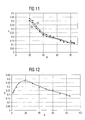
- the coupling-out efficiency ⁇ of a semiconductor chip with a single mesa 4 was calculated, with all the phontonts entering the cover layer 5 being absorbed by the cover layer 5.
- the aperiodic case is in FIG. 11 represented by the curve 36. Out FIG. 11 It can already be seen that the cover layer 5 provides a noticeable contribution to the coupling-out efficiency ⁇ .
- flank angle ⁇ there is also an optimum range. This is based on FIG. 12 clear.
- the radius r p was set equal to 10 ⁇ m.
- the radius r a of the active zone 3 and the radius r n of the base surface 24 were varied so that the angle of attack ⁇ of the flanks 27 and 26 covers a range of values between 1.5 ° and 85 °. How out FIG. 12 is recognizable, there is an optimum angle range for the angle of attack ⁇ .
- the flank angle ⁇ should be between 5 ° and 60 °, preferably between 10 ° and 40 °. Particularly good values for the coupling-out efficiency ⁇ are obtained when the angle of attack ⁇ is between 15 ° and 30 °.
- a curve 37 in FIG. 13 illustrates the case that the reflectivity R K of the pad 25 is 0.3.
- Another curve 38 relates to the case where the reflectivity R K of the pad 25 is 0.8.
- Both the curve 37 and the curve 38 show the dependence of the coupling efficiency ⁇ on the diameter 2r a of the active zone 3. With good reflectivity of the pad 25, the coupling-out efficiency ⁇ decreases only slightly with increasing diameter of the active zone 3.
- the curve 37 the realistic case of a bad Reflectance R K of the contact point 25 illustrates, however, shows that the coupling-out efficiency ⁇ decreases sharply with increasing diameter of the active zone 3.
- the decoupling efficiency ⁇ is therefore the better the smaller the lateral extent of the meseneses 4.
- the thickness of the cover layer 5 is also important for the coupling-out efficiency ⁇ .
- the decoupling efficiency ⁇ is plotted for different cases as a function of the thickness h w of the cover layer 5.
- a curve 39 represents the already mentioned periodic case.
- a further curve 40 relates to the aperiodic case and a third curve 41 to a case in which square semiconductor chips having an edge length of 300 ⁇ m are interconnected by a connecting layer.
- the cover layer 5 is increasingly advantageous with increasing layer thickness.
- the layer thickness h w is smaller than the height of the mesenes 4, which in the present case is 6 ⁇ m . It follows that the depth of the cavities 8 should be greater than half the thickness of the active thin film layer 2.
- FIG. 15 shows a preferred embodiment of a thin-film LED chip in a schematic representation.
- the thin-film layer 2 consists of a highly doped with Te n-InGaAlP layer 2a (concentration> 10 17 cm -3, preferably> 10 18 cm -3) with a film thickness of about 4 ⁇ m and a Mg-doped p-GaP Layer 2b with a layer thickness of about 3.5 ⁇ m.
- an insulating layer 9, for example, Si 3 N 4 and a metallic reflector contact layer 10 is applied on the attachment side 11 of the thin-film layer 2 facing the carrier substrate 1, as in connection with FIG Fig. 1 described.
- the Si 3 N 4 - layer which has a thickness of preferably about three wavelengths of the emitted radiation based on the wavelength of the light emitted by the active zone, leads in addition to their electrical insulation effect to an improved mirror effect of the metallic reflector and provides when using a suitable material at the same time a diffusion barrier between thin film layer 2 and metallic reflector layer 10 is.
- the insulating layer 9 may alternatively be a layer stack of, for example, alternating silicon nitride layers and silicon oxide layers.
- the p-side power supply to the active zone 3 is ensured by an alloyed AuZn contacts 12 which are arranged on the carrier substrate 1 facing surface of the mesenes 4 and passed through the insulating layer 9.
- the reflector contact layer 10 is preferably an AuZn / TiW (N) / Au layer. But it can also be made entirely of Au, Al or Ag or an alloy of these metals.
- the thin-film layer 2 is applied by bonding to the conductive carrier substrate 1, in the exemplary embodiment an n-GaAs substrate.
- Top and bottom of the carrier substrate 1 are provided, for example, with AuGe contact layers 44, 45.
- a TiPtAu / AuSn layer 47 is additionally present on the AuGe contact layer 45, for example.
- a center contact 7 and a metal frame 43 or other electrically conductive frame is provided, which is connected via two electrically conductive webs, not shown, with the center contact 7.
- the center contact 7 and the metal frame 43 are made of, for example, a TiPtAu layer and a TiAuGe layer interposed therebetween and the thin film layer 2.
- the high conductivity of the n-InGaAlP layer ensures the required current spreading.
- an optical tempering layer 42 is arranged on the front side of the thin film layer 2, in the exemplary embodiment a ⁇ / 4 layer of Si 3 N 4 .
- a plurality of pyramidal truncated cavities 8 are formed, which significantly increase the light extraction of the light emitting diode.
- the cavities 8 extend so far into the thin-film layer 2 that they interrupt the pn junction 3.
- the cavities 8 can also be designed so deep that they do not sever the pn junction.
- the cavities 8 additionally have the advantage that they significantly reduce the stresses occurring during eutectic bonding of the thin-film layer 2 to the carrier substrate 1 due to the different thermal expansion coefficients of the various materials. Thus, process reliability and manufacturing yield are increased.
- FIG. 16 shows a further semiconductor chip in a schematic representation.
- the thin film layer 2 is mounted on an electrically insulating support substrate 1 so that the power supply to the p-side of the pn junction 3 via one adjacent to the thin film layer 2 arranged on the Au-Ge contact layer 45 arranged p-contact 46.
- the p-InGaAlP layer 2b has a thickness of 6 ⁇ m, with 1 x 10 18 cm -3-doped n-InGaAlP: Te - layer 2 has a thickness of 3 ⁇ m.
- the cavities 8 in this embodiment extend to a depth of 5.5 ⁇ m . They do not interrupt the pn junction 3 in this embodiment.
- an optical tempering layer 48 made of conductive indium-tin oxide is attached by way of example in this embodiment, which also contributes to the expansion of the current in addition to the improvement of the light outcoupling. Consequently, the n-layer 2a may possibly be made thinner here than when using an electrically insulating tempering layer, because then the current widening does not have to take place exclusively in the thin-film layer 2.
- Such an electrically conductive tempering layer 48 can also be used in all other embodiments of the semiconductor chip.
- an insulating tempering layer 42 may be used instead of the indium tin oxide layer 48.
- the structure shown is also suitable when using a conductive carrier substrate 1 and is not limited to the use of an electrically insulating carrier substrate 1.
- the structure of the embodiment of FIG. 16 has the advantage that the carrier substrate 1 can advantageously be optimized in particular with regard to thermal expansion and / or thermal conductivity, without having to pay attention to its electrical conductivity.
- the cavities 8 can be filled with a suitable material for processing the thin-film layer.
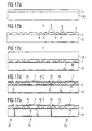
- FIGS. 17a to 17e 3 illustrates a process of simultaneously producing a plurality of semiconductor chips showing schematic representations of vertical cuts through a wafer at different times in the manufacturing process.
- the active thin film layer 2 as well as the layers explained above between the carrier substrate and the thin film layer with all its details has been described here and also in the descriptions of the methods of the FIGS. 18a to 19e omitted for simplicity.
- the thin-film layer 2, the insulating layer 9, the contact layers 7, 43-47 and 49 and the tempering layer 42, 48 are produced, for example, by conventional deposition methods known in the semiconductor art.
- an active thin-film layer 2 is grown on a growth substrate 20 ( Figure 17a ).
- a thin film layer 2 typically comprises a plurality of semiconductor layers of different compositions.
- the cavities 8 are formed. This is done for example by a suitable mask technique and anisotropic wet chemical etching ( FIG. 17b ).
- the reflective layer 9,10 (not shown here, but see for example the FIGS. 15 and 16 ) are applied and the vias 4 are the vias 12 (not shown here, but see for example Figures 15 and 16) made before this page below is connected to a carrier substrate wafer 21, on the main surfaces of which contact layers 44, 45 are preferably located ( FIG. 17c ).
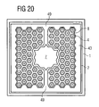
- a bond pad 7 is applied to the exposed surface of the thin film layer 2 in each surface region in which a semiconductor chip is to be formed, with the connection webs 49 (see FIG. 20 ) a power supply frame 43 is connected, which runs at the outer edge of the thin film layer 2 of the later chip. Exemplary materials of such contact layers are already mentioned above.
- the radiation decoupling surfaces of the later chips, which are located between the bonding pads 7 and the contacting frame 70, are provided with an optical coating layer 42. Compare to this FIG. 17d ,
- the thin-film layer 2 is preferably severed along the separation paths 22 by means of etching and, if necessary, a damage etching is carried out on the resulting flanks of the thin-film layer.
- the flanks of the thin film layer 2 may, if necessary, be provided with a tempering layer and / or passivation layer.
- the carrier substrate wafer 21 is then severed, for example, by means of sawing or scribing and breaking along the separation paths 22, so that individual semiconductor chips 23 are formed.
- the complete production of the semiconductor chips is thus advantageously carried out in the laminated pane; that is, the separation of the wafer into individual chips is the last step of the process, before the chips are mounted into packages at a later time, for example.
- FIGS. 18a to 18e The method illustrated differs from that of FIGS. 17a-17e essentially by omitting the separate severing of the thin film layer 2 before cutting the carrier substrate wafer 21 and cutting the thin film layer 2 together with the cutting of the carrier substrate wafer 21 along the dividing lines 22 in one step.
- FIGS. 19a to 19e The method illustrated differs from that of FIGS. 17a-17e essentially in that the separate severing of the thin-film layer 2 takes place before the thin-film layer 2 is connected to the carrier substrate wafer 21.
- the removal of the growth substrate can also be done by means of blowing off instead of by means of grinding and / or wet-chemical etching.
- an absorbing layer is preferably introduced between the thin film layer and the growth substrate, which has a smaller band gap than the growth substrate.
- the absorbing layer is destroyed by means of a laser of suitable wavelength.
- the absorbing layer is InGaAs, and the laser is an IR laser, for example.
- the meseneses 4 produced by means of cavities 8 are visible. It can be seen in particular that in the areas of the contact 7, the connecting webs 49, the power supply frame 43 and the separation tracks no cavities 8 are present. These are all areas in which no or only little radiation would be decoupled anyway. The omission of the cavities in these areas advantageously leads to a clear mechanical stabilization of the thin-film layer 2. This has a positive effect, in particular in the area of the contact 7, because there during the assembly of the Semiconductor chips in a housing usually a bonding wire is placed and pressed.
- FIG. 21 shows an oblique view of a surface of a thin-film layer 2 after the cavities 8 have been formed.
- FIG. 22 shows an enlarged section of FIG. 21 .
Landscapes
- Engineering & Computer Science (AREA)
- Manufacturing & Machinery (AREA)
- Computer Hardware Design (AREA)
- Microelectronics & Electronic Packaging (AREA)
- Power Engineering (AREA)
- Led Devices (AREA)
- Led Device Packages (AREA)
Claims (26)
- Puce de semi-conducteur émettant un rayonnement avec une couche à film mince (2), dans laquelle est formée une zone (3) d'émission de photons,
dans laquelle la couche à film mince (2) présente, sur une face orientée à l'opposé d'une direction de rayonnement de la puce de semi-conducteur, au moins une cavité par laquelle une multiplicité de mésas sont formées, et est disposée sur un substrat de support non utilisé comme son substrat de croissance et est assemblée à celui-ci,
caractérisée en ce que la couche à film mince (2) présente une couche de recouvrement (5) reliant les mésas les unes aux autres, dans laquelle la zone (3) émettant des photons est disposée à l'extérieur des mésas, au moins une trajectoire (18) des photons émis par la zone active (3) conduit de la mésa respective (4) jusqu'à une des mésas voisines (4), et
les mésas (4) sont recouvertes d'une couche de réflexion (9, 10), de telle manière que tous les rayons lumineux arrivant sur une face latérale des mésas (4) soient déviés en direction d'un côté de sortie (6) de la puce de semi-conducteur. - Puce de semi-conducteur selon la revendication 1, caractérisé en ce que la section transversale de la cavité (8) diminue en s'éloignant du substrat de support (1).
- Puce de semi-conducteur selon la revendication 1 ou 2, caractérisée en ce que la couche à film mince active présente une succession de couches sur la base de In1-x-yAlxGayP (dans laquelle 0≤x≤1, 0≤y≤1 et x+y≤1).
- Puce de semi-conducteur selon l'une quelconque des revendications précédentes, caractérisée en ce que des mesas (4) sont formées par une multiplicité de cavités (8), uniquement dans des régions qui représentent des régions d'émission de rayonnement de la couche à film mince (2).
- Puce de semi-conducteur selon la revendication 4 ou 1, caractérisée en ce que les mésas (4) se rétrécissent en direction du substrat de support.
- Puce de semi-conducteur selon la revendication 5, caractérisée en ce que les mésas (4) présentent des faces latérales concaves (13).
- Puce de semi-conducteur selon l'une quelconque des revendications 4 à 6, caractérisée en ce que les mésas (4) sont réalisées en forme de tronc de pyramide.
- Puce de semi-conducteur selon l'une quelconque des revendications précédentes, caractérisée en ce que la couche de recouvrement (5) est transparente pour les photons émis par la zone d'émission de photons (3).
- Puce de semi-conducteur selon l'une quelconque des revendications précédentes, caractérisée en ce que la couche de recouvrement (5) est dopée.
- Puce de semi-conducteur selon la revendication 1, caractérisée en ce que la couche de réflexion présente une couche de métallisation (10) avec une couche d'isolation sous-jacente (9).
- Puce de semi-conducteur selon l'une quelconque des revendications précédentes, caractérisée en ce que la couche à film mince active (2) présente une épaisseur comprise entre 5 µm et 50 µm.
- Puce de semi-conducteur selon la revendication 11, caractérisée en ce que la couche à film mince active (2) présente une épaisseur comprise entre 5 µm et 25 µm.
- Puce de semi-conducteur selon l'une quelconque des revendications précédentes, caractérisée en ce que la profondeur de ladite au moins une cavité (8) est plus grande que la moitié de l'épaisseur de la couche à film mince (2).
- Puce de semi-conducteur selon l'une quelconque des revendications précédentes, caractérisée en ce que le substrat de support (1) est électriquement conducteur et présente une face de contact électrique (44) sur le côté orienté à l'opposé de la couche à film mince (2).
- Puce de semi-conducteur selon l'une quelconque des revendications 1 à 13, caractérisée en ce que le substrat de support (1) est électriquement isolant ou électriquement conducteur et présente une face de contact électrique (46) à côté de la couche à film mince (2) sur le côté orienté vers la couche à film mince (2).
- Puce de semi-conducteur selon l'une quelconque des revendications précédentes, caractérisée en ce que la surface (6) de la couche à film mince (2) qui fait face au côté de fixation (11) est munie d'une couche antireflet optique (42) pour la sortie améliorée de la lumière.
- Puce de semi-conducteur selon la revendication 16, caractérisée en ce que la couche antireflet optique (42) est formée de nitrure de silicium.
- Puce de semi-conducteur selon la revendication 16, caractérisée en ce que la couche antireflet optique (42) est formée d'oxyde d'indium-étain conducteur.
- Puce de semi-conducteur selon l'une quelconque des revendications précédentes, caractérisée en ce que la couche à film mince (2) ne présente aucune cavité (8) dans la région située en face d'un ou de plusieurs point (s) de contact (7, 43).
- Puce de semi-conducteur selon l'une quelconque des revendications précédentes, caractérisée en ce que les mésas (4) se rétrécissent en direction du substrat de support (1).
- Puce de semi-conducteur selon la revendication 20, caractérisée en ce que les mésas (4) présentent une forme de tronc de pyramide ou de tronc de cône et les faces latérales inclinées présentent un angle d'inclinaison ϕ compris entre 5° et 60° par rapport à la direction d'extension de la couche à film mince (2).
- Puce de semi-conducteur selon la revendication 21, caractérisée en ce que l'angle d'inclinaison ϕ est compris entre 15° et 30°.
- Procédé pour la fabrication simultanée d'une multiplicité de puces de semi-conducteur pour l'optoélectronique avec une couche à film mince (2), dans laquelle est formée une zone d'émission de photons (3), comprenant les étapes de procédé suivantes:- croissance épitaxiale d'une succession de couches contenant la zone d'émission de photons (3) sur un substrat de croissance (20);- formation d'au moins une cavité (8) dans la succession de couches, de telle manière qu'il apparaisse une multiplicité de mésas (4) dans la succession de couches, la cavité étant formée avec une faible profondeur telle que la succession de couches présente une couche de recouvrement (5) reliant les mésas les unes aux autres, dans laquelle la zone d'émission de photons (3) est disposée à l'extérieur des mésas;- dépôt d'une couche de réflexion sur le côté de la succession de couches muni des cavités (8);- dépôt du composite de tranches composé du substrat de croissance (20) et de la succession de couches sur un substrat de support (21), de telle manière que les mésas (4) soient tournées vers le substrat de support (21), et liaison du composite de tranches avec le substrat de support (21);- enlèvement au moins partiel du substrat de croissance (20);- dépôt d'un contact électrique (7, 43, 49) sur le côté de la succession de couches qui fait face aux mésas (4); et- séparation du composite composé du substrat de support (21) et de la succession de couches structurée le long de traces de séparation (22) en puces de semi-conducteur (23),
caractérisé en ce que- l'on exécute les étapes du procédé dans l'ordre indiqué. - Procédé selon la revendication 23, dans lequel on dépose au moins une couche d'isolation (9) sur la surface de la succession de couches munie des cavités (8) et on réalise respectivement au moins un contact traversant (12) sur les mésas (4).
- Procédé selon l'une des revendications 23 à 24, dans lequel on sépare la succession de couches le long des traces de séparation (22) avant la liaison de la succession de couches avec le substrat de support (21).
- Procédé selon la revendication 25, dans lequel on enlève au moins partiellement le substrat de croissance (20) avant la liaison et on sépare ensuite la succession de couches le long des traces de séparation (22) dans une étape séparée, avant la coupe du substrat de support (21).
Priority Applications (2)
| Application Number | Priority Date | Filing Date | Title |
|---|---|---|---|
| EP17173235.7A EP3240048B1 (fr) | 2000-08-08 | 2001-08-08 | Puce semi-conductrice pour l'optoélectronique et son procédé de fabrication |
| EP10183569.2A EP2267800B1 (fr) | 2000-08-08 | 2001-08-08 | Puce semi-conductrice pour l'optoélectronique et son procédé de fabrication |
Applications Claiming Priority (5)
| Application Number | Priority Date | Filing Date | Title |
|---|---|---|---|
| DE10038671A DE10038671A1 (de) | 2000-08-08 | 2000-08-08 | Halbleiterchip für die Optoelektronik |
| DE10038671 | 2000-08-08 | ||
| DE10059532 | 2000-11-30 | ||
| DE10059532A DE10059532A1 (de) | 2000-08-08 | 2000-11-30 | Halbleiterchip für die Optoelektronik |
| PCT/DE2001/003033 WO2002013281A1 (fr) | 2000-08-08 | 2001-08-08 | Puce de semi-conducteur pour optoelectronique et son procede de fabrication |
Related Child Applications (3)
| Application Number | Title | Priority Date | Filing Date |
|---|---|---|---|
| EP10183569.2A Division EP2267800B1 (fr) | 2000-08-08 | 2001-08-08 | Puce semi-conductrice pour l'optoélectronique et son procédé de fabrication |
| EP10183569.2A Division-Into EP2267800B1 (fr) | 2000-08-08 | 2001-08-08 | Puce semi-conductrice pour l'optoélectronique et son procédé de fabrication |
| EP17173235.7A Division EP3240048B1 (fr) | 2000-08-08 | 2001-08-08 | Puce semi-conductrice pour l'optoélectronique et son procédé de fabrication |
Publications (2)
| Publication Number | Publication Date |
|---|---|
| EP1307928A1 EP1307928A1 (fr) | 2003-05-07 |
| EP1307928B1 true EP1307928B1 (fr) | 2014-12-31 |
Family
ID=26006634
Family Applications (1)
| Application Number | Title | Priority Date | Filing Date |
|---|---|---|---|
| EP01984505.6A Expired - Lifetime EP1307928B1 (fr) | 2000-08-08 | 2001-08-08 | Puce de semi-conducteur pour optoelectronique et son procede de fabrication |
Country Status (6)
| Country | Link |
|---|---|
| US (4) | US20020017652A1 (fr) |
| EP (1) | EP1307928B1 (fr) |
| JP (2) | JP4230219B2 (fr) |
| CN (1) | CN100565942C (fr) |
| TW (1) | TW516246B (fr) |
| WO (1) | WO2002013281A1 (fr) |
Families Citing this family (173)
| Publication number | Priority date | Publication date | Assignee | Title |
|---|---|---|---|---|
| US6410942B1 (en) * | 1999-12-03 | 2002-06-25 | Cree Lighting Company | Enhanced light extraction through the use of micro-LED arrays |
| US20020017652A1 (en) * | 2000-08-08 | 2002-02-14 | Stefan Illek | Semiconductor chip for optoelectronics |
| US6946788B2 (en) | 2001-05-29 | 2005-09-20 | Toyoda Gosei Co., Ltd. | Light-emitting element |
| US7135711B2 (en) * | 2001-08-30 | 2006-11-14 | Osram Opto Semiconductors Gmbh | Electroluminescent body |
| DE10148227B4 (de) * | 2001-09-28 | 2015-03-05 | Osram Opto Semiconductors Gmbh | Strahlungsemittierender Halbleiterchip, Verfahren zu dessen Herstellung und strahlungsemittierendes Bauelement |
| ATE445233T1 (de) * | 2002-01-28 | 2009-10-15 | Nichia Corp | Nitrid-halbleiterbauelement mit einem trägersubstrat und verfahren zu seiner herstellung |
| KR101030068B1 (ko) * | 2002-07-08 | 2011-04-19 | 니치아 카가쿠 고교 가부시키가이샤 | 질화물 반도체 소자의 제조방법 및 질화물 반도체 소자 |
| DE10234977A1 (de) * | 2002-07-31 | 2004-02-12 | Osram Opto Semiconductors Gmbh | Strahlungsemittierendes Dünnschicht-Halbleiterbauelement auf GaN-Basis |
| US7511311B2 (en) | 2002-08-01 | 2009-03-31 | Nichia Corporation | Semiconductor light-emitting device, method for manufacturing the same, and light-emitting apparatus including the same |
| US6929966B2 (en) * | 2002-11-29 | 2005-08-16 | Osram Opto Semiconductors Gmbh | Method for producing a light-emitting semiconductor component |
| DE10307280B4 (de) * | 2002-11-29 | 2005-09-01 | Osram Opto Semiconductors Gmbh | Verfahren zum Herstellen eines lichtemittierenden Halbleiterbauelements |
| DE10261364B4 (de) * | 2002-12-30 | 2004-12-16 | Osram Opto Semiconductors Gmbh | Verfahren zur Herstellung einer temperbarer Mehrschichtkontaktbeschichtung, insbesondere einer temperbaren Mehrschichtkontaktmetallisierung |
| DE10308322B4 (de) * | 2003-01-31 | 2014-11-06 | Osram Opto Semiconductors Gmbh | Verfahren zum Herstellen eines elektrischen Kontaktbereiches auf einer Halbleiterschicht und Bauelement mit derartigem Kontaktbereich |
| JP4691014B2 (ja) | 2003-02-26 | 2011-06-01 | カリダ ゲノミクス,インコーポレーテッド | ハイブリダイゼーションによるランダムアレイdna分析 |
| DE10308866A1 (de) * | 2003-02-28 | 2004-09-09 | Osram Opto Semiconductors Gmbh | Beleuchtungsmodul und Verfahren zu dessen Herstellung |
| TWI330413B (en) | 2005-01-25 | 2010-09-11 | Epistar Corp | A light-emitting device |
| US8063557B2 (en) * | 2003-07-04 | 2011-11-22 | Epistar Corporation | Light-emitting device having wavelength-converting materials therewithin |
| CN100499184C (zh) * | 2003-09-26 | 2009-06-10 | 奥斯兰姆奥普托半导体有限责任公司 | 发光薄膜半导体芯片 |
| DE102004016697B4 (de) * | 2004-02-27 | 2007-10-11 | Osram Opto Semiconductors Gmbh | Verfahren zum Herstellen von Halbleiterchips umfassend ein Verbindungsverfahren, das Löten mit einem Lot umfasst, und Halbleiterchip |
| TWI244221B (en) * | 2004-03-01 | 2005-11-21 | Epistar Corp | Micro-reflector containing flip-chip light emitting device |
| JP4868709B2 (ja) * | 2004-03-09 | 2012-02-01 | 三洋電機株式会社 | 発光素子 |
| US7064356B2 (en) | 2004-04-16 | 2006-06-20 | Gelcore, Llc | Flip chip light emitting diode with micromesas and a conductive mesh |
| DE102004021175B4 (de) * | 2004-04-30 | 2023-06-29 | OSRAM Opto Semiconductors Gesellschaft mit beschränkter Haftung | Halbleiterchips für die Optoelektronik und Verfahren zu deren Herstellung |
| DE102004040277B4 (de) * | 2004-06-30 | 2015-07-30 | Osram Opto Semiconductors Gmbh | Reflektierendes Schichtsystem mit einer Mehrzahl von Schichten zur Aufbringung auf ein III/V-Verbindungshalbleitermaterial |
| JP5305655B2 (ja) * | 2004-07-30 | 2013-10-02 | オスラム オプト セミコンダクターズ ゲゼルシャフト ミット ベシュレンクテル ハフツング | 薄膜技術による半導体チップの製造方法および薄膜半導体チップ |
| US8728937B2 (en) * | 2004-07-30 | 2014-05-20 | Osram Opto Semiconductors Gmbh | Method for producing semiconductor chips using thin film technology |
| TWI442456B (zh) * | 2004-08-31 | 2014-06-21 | Sophia School Corp | 發光元件 |
| DE102004046792B4 (de) * | 2004-09-27 | 2023-01-19 | OSRAM Opto Semiconductors Gesellschaft mit beschränkter Haftung | Optoelektronischer Dünnfilmchip mit integrierter Linse und Verfahren zu seiner Herstellung |
| US7352006B2 (en) * | 2004-09-28 | 2008-04-01 | Goldeneye, Inc. | Light emitting diodes exhibiting both high reflectivity and high light extraction |
| DE102004061865A1 (de) * | 2004-09-29 | 2006-03-30 | Osram Opto Semiconductors Gmbh | Verfahren zur Herstellung eines Dünnfilmhalbleiterchips |
| US20060104061A1 (en) * | 2004-11-16 | 2006-05-18 | Scott Lerner | Display with planar light source |
| DE102006002275A1 (de) | 2005-01-19 | 2006-07-20 | Osram Opto Semiconductors Gmbh | Beleuchtungseinrichtung |
| JP2006235415A (ja) * | 2005-02-28 | 2006-09-07 | Hitachi Displays Ltd | レンズアレイおよびそれを利用した表示装置 |
| US20060237735A1 (en) * | 2005-04-22 | 2006-10-26 | Jean-Yves Naulin | High-efficiency light extraction structures and methods for solid-state lighting |
| KR100597166B1 (ko) * | 2005-05-03 | 2006-07-04 | 삼성전기주식회사 | 플립 칩 발광다이오드 및 그 제조방법 |
| EP1727216B1 (fr) * | 2005-05-24 | 2019-04-24 | LG Electronics, Inc. | Diode électroluminescente à bâtonnets et procédé de fabrication correspondant |
| DE102005033005A1 (de) * | 2005-07-14 | 2007-01-18 | Osram Opto Semiconductors Gmbh | Optoelektronischer Chip |
| DE102005035722B9 (de) | 2005-07-29 | 2021-11-18 | OSRAM Opto Semiconductors Gesellschaft mit beschränkter Haftung | Optoelektronischer Halbleiterchip und Verfahren zu dessen Herstellung |
| DE102005062514A1 (de) | 2005-09-28 | 2007-03-29 | Osram Opto Semiconductors Gmbh | Optoelektronisches Bauelement |
| DE102005061346A1 (de) * | 2005-09-30 | 2007-04-05 | Osram Opto Semiconductors Gmbh | Optoelektronischer Halbleiterchip |
| DE102005046942A1 (de) | 2005-09-30 | 2007-04-05 | Osram Opto Semiconductors Gmbh | Verfahren zur Verbindung von Schichten, entsprechendes Bauelement und organische Leuchtdiode |
| DE102005047149A1 (de) * | 2005-09-30 | 2007-04-12 | Osram Opto Semiconductors Gmbh | Epitaxiesubstrat, damit hergestelltes Bauelement sowie entsprechende Herstellverfahren |
| DE102005047152A1 (de) * | 2005-09-30 | 2007-04-12 | Osram Opto Semiconductors Gmbh | Epitaxiesubstrat, Verfahren zu seiner Herstellung und Verfahren zur Herstellung eines Halbleiterchips |
| JP2007103725A (ja) * | 2005-10-05 | 2007-04-19 | Toshiba Corp | 半導体発光装置 |
| KR101316415B1 (ko) * | 2005-10-17 | 2013-10-08 | 엘지이노텍 주식회사 | 질화물 반도체 발광소자 및 그 제조 방법 |
| JP4857733B2 (ja) * | 2005-11-25 | 2012-01-18 | パナソニック電工株式会社 | 半導体発光素子およびその製造方法 |
| KR100714123B1 (ko) * | 2005-12-08 | 2007-05-02 | 한국전자통신연구원 | 실리콘 발광소자 |
| DE102006033893B4 (de) | 2005-12-16 | 2017-02-23 | Osram Opto Semiconductors Gmbh | Beleuchtungseinrichtung |
| DE102006033894B4 (de) * | 2005-12-16 | 2019-05-09 | Osram Gmbh | Beleuchtungseinrichtung und Anzeigegerät mit einer Beleuchtungseinrichtung |
| JP2007173579A (ja) * | 2005-12-22 | 2007-07-05 | Matsushita Electric Works Ltd | 半導体発光素子およびその製造方法 |
| US20100084679A1 (en) * | 2006-01-06 | 2010-04-08 | Epistar Corporation | Light-emitting device |
| US20080128734A1 (en) * | 2006-01-06 | 2008-06-05 | Epistar Corporation | Light-emitting device |
| KR20070088145A (ko) * | 2006-02-24 | 2007-08-29 | 엘지전자 주식회사 | 발광 다이오드 및 그 제조방법 |
| DE102006031076A1 (de) * | 2006-03-17 | 2007-09-20 | Osram Opto Semiconductors Gmbh | Optisches Projektionsgerät |
| DE102006024220A1 (de) * | 2006-04-13 | 2007-10-18 | Osram Opto Semiconductors Gmbh | Optoelektronisches Halbleiterbauelement |
| DE102006061167A1 (de) | 2006-04-25 | 2007-12-20 | Osram Opto Semiconductors Gmbh | Optoelektronisches Halbleiterbauelement |
| DE102006034847A1 (de) * | 2006-04-27 | 2007-10-31 | Osram Opto Semiconductors Gmbh | Optoelektronischer Halbleiterchip |
| DE102006028692B4 (de) * | 2006-05-19 | 2021-09-02 | OSRAM Opto Semiconductors Gesellschaft mit beschränkter Haftung | Elektrisch leitende Verbindung mit isolierendem Verbindungsmedium |
| US20070291494A1 (en) * | 2006-06-20 | 2007-12-20 | Galli Robert D | Led reflector assembly for improving the color rendering index of the light output |
| US20080030974A1 (en) * | 2006-08-02 | 2008-02-07 | Abu-Ageel Nayef M | LED-Based Illumination System |
| KR100809236B1 (ko) * | 2006-08-30 | 2008-03-05 | 삼성전기주식회사 | 편광 발광 다이오드 |
| DE102007004302A1 (de) | 2006-09-29 | 2008-04-03 | Osram Opto Semiconductors Gmbh | Halbleiterchip und Verfahren zur Herstellung eines Halbleiterchips |
| KR100887139B1 (ko) * | 2007-02-12 | 2009-03-04 | 삼성전기주식회사 | 질화물 반도체 발광소자 및 제조방법 |
| DE102007008524A1 (de) * | 2007-02-21 | 2008-08-28 | Osram Opto Semiconductors Gmbh | Strahlung emittierender Chip mit mindestens einem Halbleiterkörper |
| JP4896788B2 (ja) * | 2007-03-28 | 2012-03-14 | 富士通株式会社 | 半導体発光素子およびその製造方法 |
| DE102007022947B4 (de) * | 2007-04-26 | 2022-05-05 | OSRAM Opto Semiconductors Gesellschaft mit beschränkter Haftung | Optoelektronischer Halbleiterkörper und Verfahren zur Herstellung eines solchen |
| US20080303033A1 (en) * | 2007-06-05 | 2008-12-11 | Cree, Inc. | Formation of nitride-based optoelectronic and electronic device structures on lattice-matched substrates |
| JP5123573B2 (ja) * | 2007-06-13 | 2013-01-23 | ローム株式会社 | 半導体発光素子およびその製造方法 |
| KR100872717B1 (ko) | 2007-06-22 | 2008-12-05 | 엘지이노텍 주식회사 | 발광 소자 및 그 제조방법 |
| DE102007029369A1 (de) | 2007-06-26 | 2009-01-02 | Osram Opto Semiconductors Gmbh | Optoelektronisches Halbleiterbauelement und Verfahren zur Herstellung eines optoelektronischen Halbleiterbauelements |
| DE102007029391A1 (de) | 2007-06-26 | 2009-01-02 | Osram Opto Semiconductors Gmbh | Optoelektronischer Halbleiterchip |
| US20090050905A1 (en) * | 2007-08-20 | 2009-02-26 | Abu-Ageel Nayef M | Highly Efficient Light-Emitting Diode |
| DE102007039291A1 (de) | 2007-08-20 | 2009-02-26 | Osram Opto Semiconductors Gmbh | Optoelektronisches Halbleitermodul und Verfahren zur Herstellung eines solchen |
| DE102008005344A1 (de) | 2007-09-21 | 2009-04-02 | Osram Opto Semiconductors Gmbh | Strahlungsemittierendes Bauelement |
| DE102007046027A1 (de) | 2007-09-26 | 2009-04-02 | Osram Opto Semiconductors Gmbh | Optoelektronischer Halbleiterchip mit einer Mehrfachquantentopfstruktur |
| DE102007057756B4 (de) | 2007-11-30 | 2022-03-10 | OSRAM Opto Semiconductors Gesellschaft mit beschränkter Haftung | Verfahren zur Herstellung eines optoelektronischen Halbleiterkörpers |
| DE102007057672A1 (de) | 2007-11-30 | 2009-06-04 | Osram Opto Semiconductors Gmbh | Optoelektronischer Halbleiterkörper |
| DE102007061140A1 (de) | 2007-12-19 | 2009-06-25 | Osram Opto Semiconductors Gmbh | Optoelektronisches Bauelement mit Kühlelement |
| DE102008008599A1 (de) | 2007-12-20 | 2009-06-25 | Osram Opto Semiconductors Gmbh | Halbleiteranordnung, insbesondere Leuchtdiodenanordnung und Leuchtmittelanordnung |
| DE102007062046B4 (de) | 2007-12-21 | 2023-09-07 | OSRAM Opto Semiconductors Gesellschaft mit beschränkter Haftung | Lichtemittierende Bauelementeanordnung, lichtemittierendes Bauelement sowie Verfahren zum Herstellen einer Mehrzahl von lichtemittierenden Bauelementen |
| DE102008019902A1 (de) | 2007-12-21 | 2009-06-25 | Osram Opto Semiconductors Gmbh | Optoelektronisches Bauelement und Herstellungsverfahren für ein optoelektronisches Bauelement |
| US20090166654A1 (en) * | 2007-12-31 | 2009-07-02 | Zhiyin Gan | Light-emitting diode with increased light efficiency |
| DE102008003182A1 (de) | 2008-01-04 | 2009-07-09 | Osram Opto Semiconductors Gmbh | Optoelektronisches Bauelement |
| DE102008005497A1 (de) | 2008-01-22 | 2009-07-23 | Osram Opto Semiconductors Gmbh | Optoelektronisches Bauelement und Verfahren zur Herstellung eines optoelektronischen Bauelements und eines Wafers |
| DE102008012407A1 (de) | 2008-01-31 | 2009-08-06 | Osram Opto Semiconductors Gmbh | Strahlungsemittierende Vorrichtung |
| DE102008006988A1 (de) * | 2008-01-31 | 2009-08-06 | Osram Opto Semiconductors Gmbh | Optoelektronisches Bauelement und Verfahren zur Herstellung eines optoelektronischen Bauelements |
| DE102008011866B4 (de) | 2008-02-29 | 2018-05-03 | Osram Opto Semiconductors Gmbh | Lichtquellenanordnung mit einer Halbleiterlichtquelle |
| DE102008016525A1 (de) | 2008-03-31 | 2009-11-26 | Osram Opto Semiconductors Gmbh | Optoelektronischer Halbleiterkörper und Verfahren zur Herstellung eines solchen |
| DE102008011848A1 (de) | 2008-02-29 | 2009-09-03 | Osram Opto Semiconductors Gmbh | Optoelektronischer Halbleiterkörper und Verfahren zur Herstellung eines solchen |
| US8643034B2 (en) | 2008-02-29 | 2014-02-04 | Osram Opto Semiconductors Gmbh | Monolithic, optoelectronic semiconductor body and method for the production thereof |
| DE102008038857A1 (de) | 2008-03-31 | 2009-10-01 | Osram Opto Semiconductors Gmbh | Beleuchtungseinrichtung |
| DE102008032318A1 (de) | 2008-03-31 | 2009-10-01 | Osram Opto Semiconductors Gmbh | Optoelektronischer Halbleiterchip und Verfahren zur Herstellung eines solchen |
| DE102008033705A1 (de) | 2008-04-07 | 2009-10-08 | Osram Opto Semiconductors Gmbh | Optoelektronische Projektionsvorrichtung |
| DE102009018603B9 (de) | 2008-04-25 | 2021-01-14 | Samsung Electronics Co., Ltd. | Leuchtvorrichtung und Herstellungsverfahren derselben |
| DE102008024485A1 (de) | 2008-05-21 | 2009-11-26 | Osram Opto Semiconductors Gmbh | Optoelektronisches Bauelement |
| DE102008038852B4 (de) | 2008-06-03 | 2024-02-01 | OSRAM Opto Semiconductors Gesellschaft mit beschränkter Haftung | Verfahren zur Herstellung eines optoelektronischen Bauelementes und optoelektronisches Bauelement |
| DE102008050538B4 (de) | 2008-06-06 | 2022-10-06 | OSRAM Opto Semiconductors Gesellschaft mit beschränkter Haftung | Optoelektronisches Bauelement und Verfahren zu dessen Herstellung |
| KR101506264B1 (ko) * | 2008-06-13 | 2015-03-30 | 삼성전자주식회사 | 발광 소자, 발광 장치 및 상기 발광 소자의 제조 방법 |
| DE102008030751A1 (de) | 2008-06-27 | 2009-12-31 | Osram Opto Semiconductors Gmbh | Strahlungsemittierender Halbleiterchip |
| DE102008030584A1 (de) | 2008-06-27 | 2009-12-31 | Osram Opto Semiconductors Gmbh | Verfahren zur Herstellung eines optoelektronischen Bauelementes und optoelektronisches Bauelement |
| KR101478334B1 (ko) * | 2008-06-30 | 2015-01-02 | 서울바이오시스 주식회사 | 발광 다이오드 및 그 제조방법 |
| US10147843B2 (en) | 2008-07-24 | 2018-12-04 | Lumileds Llc | Semiconductor light emitting device including a window layer and a light-directing structure |
| US8236582B2 (en) * | 2008-07-24 | 2012-08-07 | Philips Lumileds Lighting Company, Llc | Controlling edge emission in package-free LED die |
| DE102008035254A1 (de) | 2008-07-29 | 2010-02-11 | Osram Opto Semiconductors Gmbh | Optoelektronischer Halbleiterchip und optoelektronisches Bauteil |
| DE102008064956B3 (de) | 2008-07-29 | 2023-08-24 | OSRAM Opto Semiconductors Gesellschaft mit beschränkter Haftung | Optoelektronisches halbleiterbauelement und verfahren zur herstellung eines optoelektronischen halbleiterbauelements |
| DE102008035255B4 (de) | 2008-07-29 | 2021-10-07 | OSRAM Opto Semiconductors Gesellschaft mit beschränkter Haftung | Optoelektronisches Halbleiterbauelement und Verfahren zur Herstellung eines optoelektronischen Halbleiterbauelements |
| DE102008038750A1 (de) * | 2008-08-12 | 2010-02-18 | Osram Opto Semiconductors Gmbh | Optoelektronisches Bauelement und Verfahren zu dessen Herstellung |
| DE102008039790B4 (de) | 2008-08-26 | 2022-05-12 | OSRAM Opto Semiconductors Gesellschaft mit beschränkter Haftung | Optoelektronisches Bauelement und Verfahren zu dessen Herstellung |
| DE102008045653B4 (de) * | 2008-09-03 | 2020-03-26 | Osram Opto Semiconductors Gmbh | Optoelektronisches Bauteil |
| US7741134B2 (en) * | 2008-09-15 | 2010-06-22 | Bridgelux, Inc. | Inverted LED structure with improved light extraction |
| DE102008049398A1 (de) | 2008-09-29 | 2010-04-01 | Osram Opto Semiconductors Gmbh | Scheinwerfer mit einer Mehrzahl von Lumineszenzdiodenemittern |
| DE102008050573A1 (de) * | 2008-10-06 | 2010-04-08 | Osram Opto Semiconductors Gmbh | Verfahren zur Herstellung eines optoelektronischen Halbleiterbauelements und optoelektronisches Halbleiterbauelement |
| DE102008051048A1 (de) | 2008-10-09 | 2010-04-15 | Osram Opto Semiconductors Gmbh | Optoelektronischer Halbleiterkörper |
| DE102008057350A1 (de) | 2008-11-14 | 2010-05-20 | Osram Opto Semiconductors Gmbh | Strahlungsemittierendes Bauelement und Verfahren zu dessen Herstellung |
| JP2010134217A (ja) * | 2008-12-05 | 2010-06-17 | Sony Corp | カラーフィルタおよびその製造方法並びに発光装置 |
| KR101014045B1 (ko) * | 2009-02-18 | 2011-02-10 | 엘지이노텍 주식회사 | 발광소자 및 그 제조방법 |
| TWI404233B (zh) * | 2009-03-31 | 2013-08-01 | Epistar Corp | 光電元件及其製造方法 |
| DE112009004628A5 (de) | 2009-04-03 | 2012-05-24 | Osram Opto Semiconductors Gmbh | Verfahren zur Herstellung eines optoelektronischen Bauelements, optoelektronisches Bauelement und Bauelementanordnung mit mehreren optoelektronischen Bauelementen |
| JP2011029612A (ja) * | 2009-06-24 | 2011-02-10 | Toyoda Gosei Co Ltd | Iii族窒化物半導体発光素子 |
| DE102009032486A1 (de) * | 2009-07-09 | 2011-01-13 | Osram Opto Semiconductors Gmbh | Optoelektronisches Bauelement |
| US9196653B2 (en) | 2009-07-30 | 2015-11-24 | 3M Innovative Properties Company | Pixelated LED |
| KR101007077B1 (ko) * | 2009-11-06 | 2011-01-10 | 엘지이노텍 주식회사 | 발광소자, 발광소자 패키지 및 그 제조방법 |
| DE102009054555A1 (de) | 2009-12-11 | 2011-06-16 | Osram Opto Semiconductors Gmbh | Optoelektronischer Halbleiterchip und Verfahren zum Herstellen eines optoelektronischen Halbleiterchips |
| DE102009054784A1 (de) | 2009-12-16 | 2011-06-22 | Osram Gesellschaft mit beschränkter Haftung, 81543 | Halbleiterchip und Verfahren zum Herstellen eines Halbleiterchips |
| KR101106151B1 (ko) * | 2009-12-31 | 2012-01-20 | 서울옵토디바이스주식회사 | 발광 소자 및 그것을 제조하는 방법 |
| US8283676B2 (en) * | 2010-01-21 | 2012-10-09 | Siphoton Inc. | Manufacturing process for solid state lighting device on a conductive substrate |
| JP5733594B2 (ja) * | 2010-02-18 | 2015-06-10 | スタンレー電気株式会社 | 半導体発光装置 |
| DE102010002204A1 (de) | 2010-02-22 | 2011-08-25 | OSRAM Opto Semiconductors GmbH, 93055 | Halbleiterdiode und Verfahren zum Herstellen einer Halbleiterdiode |
| KR101014155B1 (ko) * | 2010-03-10 | 2011-02-10 | 엘지이노텍 주식회사 | 발광 소자, 발광 소자 제조방법 및 발광 소자 패키지 |
| DE102010003112A1 (de) | 2010-03-22 | 2011-09-22 | Osram Opto Semiconductors Gmbh | Verfahren zur Kontrolle einer zwischen einer Metallschicht und einer Halbleiterschicht ausgebildeten Grenzfläche |
| DE102010014667A1 (de) | 2010-04-12 | 2011-10-13 | Osram Opto Semiconductors Gmbh | Leuchtdiodenchip mit Stromaufweitungsschicht |
| JP2011233783A (ja) * | 2010-04-28 | 2011-11-17 | Mitsubishi Heavy Ind Ltd | 半導体発光素子、半導体発光素子の保護膜及びその作製方法 |
| US8154042B2 (en) * | 2010-04-29 | 2012-04-10 | Koninklijke Philips Electronics N V | Light emitting device with trenches and a top contact |
| KR20120006410A (ko) | 2010-07-12 | 2012-01-18 | 엘지이노텍 주식회사 | 발광 소자 및 그 제조방법 |
| DE102010027679A1 (de) | 2010-07-20 | 2012-01-26 | Osram Opto Semiconductors Gmbh | Optoelektronisches Bauelement |
| CN102386319B (zh) | 2010-08-30 | 2015-10-14 | 晶元光电股份有限公司 | 发光元件 |
| TW201216508A (en) * | 2010-10-06 | 2012-04-16 | Chi Mei Lighting Tech Corp | Light-emitting diode device and manufacturing method thereof |
| DE102010054068A1 (de) | 2010-12-10 | 2012-06-14 | Osram Opto Semiconductors Gmbh | Verfahren zur Herstellung eines optoelektronischen Bauelements und Bauelement |
| TWI435481B (zh) * | 2011-02-18 | 2014-04-21 | Genesis Photonics Inc | Light emitting diode device |
| DE102011012264A1 (de) | 2011-02-24 | 2012-08-30 | Osram Opto Semiconductors Gmbh | Optoelektronisches Halbleiterbauelement |
| DE102011012262A1 (de) | 2011-02-24 | 2012-08-30 | Osram Opto Semiconductors Gmbh | Optoelektronisches Halbleiterbauelement und Verfahren zur Herstellung eines optoelektronischen Halbleiterbauelements |
| JP2012044232A (ja) * | 2011-12-02 | 2012-03-01 | Toshiba Corp | 半導体発光装置 |
| JP5806608B2 (ja) * | 2011-12-12 | 2015-11-10 | 株式会社東芝 | 半導体発光装置 |
| JP5953155B2 (ja) | 2012-02-24 | 2016-07-20 | スタンレー電気株式会社 | 半導体発光装置 |
| DE102012103159A1 (de) | 2012-04-12 | 2013-10-17 | Osram Opto Semiconductors Gmbh | Strahlung emittierendes Bauelement, transparentes Material und Füllstoffpartikel sowie deren Herstellungsverfahren |
| DE102012104363A1 (de) | 2012-05-21 | 2013-11-21 | Osram Opto Semiconductors Gmbh | Optoelektronisches Bauelement und Verfahren zu dessen Herstellung |
| DE102012106812A1 (de) | 2012-07-26 | 2014-01-30 | Osram Opto Semiconductors Gmbh | Verfahren zum Vergießen von optoelektronischen Bauelementen |
| JP6052962B2 (ja) | 2012-08-03 | 2016-12-27 | スタンレー電気株式会社 | 半導体発光装置 |
| KR101997243B1 (ko) * | 2012-09-13 | 2019-07-08 | 엘지이노텍 주식회사 | 발광 소자 및 조명 시스템 |
| JP5462333B1 (ja) | 2012-09-21 | 2014-04-02 | 株式会社東芝 | 半導体発光素子及びその製造方法 |
| KR102037865B1 (ko) | 2013-02-01 | 2019-10-30 | 삼성전자주식회사 | 반도체 발광소자 및 반도체 발광소자 제조방법 |
| US9178109B2 (en) | 2013-02-17 | 2015-11-03 | Tien Yang Wang | Semiconductor light-emitting device and method of manufacturing the same |
| JP2014042062A (ja) * | 2013-10-31 | 2014-03-06 | Future Light Limited Liability Company | 発光素子 |
| US9768345B2 (en) | 2013-12-20 | 2017-09-19 | Apple Inc. | LED with current injection confinement trench |
| DE102014114194B4 (de) * | 2014-09-30 | 2023-10-19 | OSRAM Opto Semiconductors Gesellschaft mit beschränkter Haftung | Optoelektronischer Halbleiterchip und Verfahren zu dessen Herstellung |
| CN107210337B (zh) * | 2014-11-06 | 2021-06-29 | 亮锐控股有限公司 | 具有顶部接触件下方的沟槽的发光器件 |
| US9870927B2 (en) * | 2015-04-02 | 2018-01-16 | Microsoft Technology Licensing, Llc | Free-edge semiconductor chip bending |
| KR102554702B1 (ko) * | 2015-08-25 | 2023-07-13 | 쑤저우 레킨 세미컨덕터 컴퍼니 리미티드 | 발광소자 및 이를 포함하는 발광소자 패키지 |
| US11018180B2 (en) * | 2015-10-09 | 2021-05-25 | Shenzhen Xpectvision Technology Co., Ltd. | Packaging methods of semiconductor x-ray detectors |
| DE102015117662B4 (de) | 2015-10-16 | 2021-07-22 | OSRAM Opto Semiconductors Gesellschaft mit beschränkter Haftung | Optoelektronischer Halbleiterchip und Verfahren zur Herstellung eines optoelektronischen Halbleiterchips |
| CN105870264A (zh) * | 2016-03-03 | 2016-08-17 | 映瑞光电科技(上海)有限公司 | 具有倒金字塔型侧壁的GaN基LED垂直芯片结构及制备方法 |
| CN105720140A (zh) * | 2016-03-03 | 2016-06-29 | 映瑞光电科技(上海)有限公司 | GaN基LED垂直芯片结构及制备方法 |
| JP7083230B2 (ja) * | 2016-05-10 | 2022-06-10 | ローム株式会社 | 半導体発光素子 |
| DE102016115907A1 (de) | 2016-08-26 | 2018-03-01 | Osram Opto Semiconductors Gmbh | Optoelektronisches Bauelement und Verfahren zur Herstellung eines optoelektronischen Bauelements |
| CN106299084B (zh) * | 2016-08-30 | 2018-10-16 | 开发晶照明(厦门)有限公司 | Led封装结构 |
| CN109037263A (zh) * | 2017-06-09 | 2018-12-18 | 美商晶典有限公司 | 具有透光基材的微发光二极管显示模块及其制造方法 |
| JP7079106B2 (ja) | 2018-01-24 | 2022-06-01 | シャープ株式会社 | 画像表示素子、及び画像表示素子の製造方法 |
| US20230155057A1 (en) | 2020-04-08 | 2023-05-18 | Ams-Osram International Gmbh | Semiconductor Component and Process for Manufacturing a Semiconductor Component |
| DE102020114884A1 (de) | 2020-06-04 | 2021-12-09 | OSRAM Opto Semiconductors Gesellschaft mit beschränkter Haftung | Strahlungsemittierendes bauelement und verfahren zur herstellung eines strahlungsemittierenden bauelements |
| KR20220157450A (ko) * | 2020-06-11 | 2022-11-29 | 엘지전자 주식회사 | 반도체 발광소자 및 이를 이용한 디스플레이 장치 |
| DE102020116871A1 (de) | 2020-06-26 | 2021-12-30 | OSRAM Opto Semiconductors Gesellschaft mit beschränkter Haftung | Optoelektronischer halbleiterchip |
| DE102020125056A1 (de) | 2020-09-25 | 2022-03-31 | OSRAM Opto Semiconductors Gesellschaft mit beschränkter Haftung | Optoelektronisches bauelement und verfahren zur herstellung eines optoelektronischen bauelements |
| CN112864293A (zh) * | 2021-02-24 | 2021-05-28 | 江苏大学 | 一种垂直结构深紫外led芯片及其制造方法 |
Citations (1)
| Publication number | Priority date | Publication date | Assignee | Title |
|---|---|---|---|---|
| EP0977063A1 (fr) * | 1998-07-28 | 2000-02-02 | Interuniversitair Micro-Elektronica Centrum Vzw | Socle et système pour interconnection optoélectronique et méthode de fabrication d'un tel socle et système |
Family Cites Families (32)
| Publication number | Priority date | Publication date | Assignee | Title |
|---|---|---|---|---|
| DE1589099C3 (de) | 1967-09-09 | 1975-08-28 | Siemens Ag, 1000 Berlin Und 8000 Muenchen | Leuchtanordnung |
| JPS5310840B2 (fr) * | 1972-05-04 | 1978-04-17 | ||
| US4039890A (en) * | 1974-08-16 | 1977-08-02 | Monsanto Company | Integrated semiconductor light-emitting display array |
| JPS52124885A (en) * | 1976-04-12 | 1977-10-20 | Matsushita Electric Ind Co Ltd | Semiconductor light emitting device |
| DE2926803A1 (de) * | 1979-07-03 | 1981-02-12 | Licentia Gmbh | Elektrolumineszenz-anordnung |
| NZ201460A (en) * | 1981-08-17 | 1986-11-12 | Allware Agencies Ltd | Multipurpose microprocessor controlled heating and cooling fan |
| JPS5892751U (ja) * | 1981-12-17 | 1983-06-23 | 三洋電機株式会社 | 発光ダイオ−ド素子 |
| JPS61183986A (ja) * | 1985-02-08 | 1986-08-16 | Toshiba Corp | 半導体発光装置の製造方法 |
| JPH0752779B2 (ja) * | 1987-12-09 | 1995-06-05 | 日立電線株式会社 | 発光ダイオードアレイ |
| US5087949A (en) | 1989-06-27 | 1992-02-11 | Hewlett-Packard Company | Light-emitting diode with diagonal faces |
| US5008718A (en) | 1989-12-18 | 1991-04-16 | Fletcher Robert M | Light-emitting diode with an electrically conductive window |
| JPH0463478A (ja) * | 1990-07-03 | 1992-02-28 | Sanyo Electric Co Ltd | SiC発光装置 |
| JP3149030B2 (ja) * | 1991-06-13 | 2001-03-26 | 富士通株式会社 | 半導体量子箱装置及びその製造方法 |
| US5309001A (en) * | 1991-11-25 | 1994-05-03 | Sharp Kabushiki Kaisha | Light-emitting diode having a surface electrode of a tree-like form |
| JPH05327012A (ja) * | 1992-05-15 | 1993-12-10 | Sanyo Electric Co Ltd | 炭化ケイ素発光ダイオード |
| JPH06151955A (ja) * | 1992-10-29 | 1994-05-31 | Victor Co Of Japan Ltd | 半導体発光素子 |
| JPH06318731A (ja) * | 1993-03-12 | 1994-11-15 | Sharp Corp | 半導体発光装置 |
| US5376580A (en) | 1993-03-19 | 1994-12-27 | Hewlett-Packard Company | Wafer bonding of light emitting diode layers |
| US5385632A (en) * | 1993-06-25 | 1995-01-31 | At&T Laboratories | Method for manufacturing integrated semiconductor devices |
| JP3158869B2 (ja) * | 1993-06-30 | 2001-04-23 | 日立電線株式会社 | 発光ダイオード及びその製造方法 |
| TW253999B (fr) * | 1993-06-30 | 1995-08-11 | Hitachi Cable | |
| US5621225A (en) * | 1996-01-18 | 1997-04-15 | Motorola | Light emitting diode display package |
| GB9603052D0 (en) * | 1996-02-14 | 1996-04-10 | Philips Electronics Nv | Image sensor |
| US6229160B1 (en) | 1997-06-03 | 2001-05-08 | Lumileds Lighting, U.S., Llc | Light extraction from a semiconductor light-emitting device via chip shaping |
| DE59814431D1 (de) | 1997-09-29 | 2010-03-25 | Osram Opto Semiconductors Gmbh | Halbleiterlichtquelle und Verfahren zu ihrer Herstellung |
| US6091085A (en) * | 1998-02-19 | 2000-07-18 | Agilent Technologies, Inc. | GaN LEDs with improved output coupling efficiency |
| DE19911717A1 (de) | 1999-03-16 | 2000-09-28 | Osram Opto Semiconductors Gmbh | Monolithisches elektrolumineszierendes Bauelement und Verfahren zu dessen Herstellung |
| US6410942B1 (en) * | 1999-12-03 | 2002-06-25 | Cree Lighting Company | Enhanced light extraction through the use of micro-LED arrays |
| US6486499B1 (en) * | 1999-12-22 | 2002-11-26 | Lumileds Lighting U.S., Llc | III-nitride light-emitting device with increased light generating capability |
| US20020017652A1 (en) * | 2000-08-08 | 2002-02-14 | Stefan Illek | Semiconductor chip for optoelectronics |
| US6727167B2 (en) * | 2000-10-13 | 2004-04-27 | Emcore Corporation | Method of making an aligned electrode on a semiconductor structure |
| US6455878B1 (en) * | 2001-05-15 | 2002-09-24 | Lumileds Lighting U.S., Llc | Semiconductor LED flip-chip having low refractive index underfill |
-
2000
- 2000-12-27 US US09/750,004 patent/US20020017652A1/en not_active Abandoned
-
2001
- 2001-08-08 JP JP2002518539A patent/JP4230219B2/ja not_active Expired - Lifetime
- 2001-08-08 CN CNB018170358A patent/CN100565942C/zh not_active Expired - Lifetime
- 2001-08-08 WO PCT/DE2001/003033 patent/WO2002013281A1/fr active Application Filing
- 2001-08-08 TW TW090119347A patent/TW516246B/zh not_active IP Right Cessation
- 2001-08-08 EP EP01984505.6A patent/EP1307928B1/fr not_active Expired - Lifetime
- 2001-08-08 US US10/344,308 patent/US7109527B2/en not_active Expired - Lifetime
-
2003
- 2003-01-17 US US10/346,605 patent/US6995030B2/en not_active Expired - Lifetime
-
2006
- 2006-04-12 US US11/403,006 patent/US20060180820A1/en not_active Abandoned
-
2007
- 2007-03-12 JP JP2007061973A patent/JP5215575B2/ja not_active Expired - Lifetime
Patent Citations (1)
| Publication number | Priority date | Publication date | Assignee | Title |
|---|---|---|---|---|
| EP0977063A1 (fr) * | 1998-07-28 | 2000-02-02 | Interuniversitair Micro-Elektronica Centrum Vzw | Socle et système pour interconnection optoélectronique et méthode de fabrication d'un tel socle et système |
Also Published As
| Publication number | Publication date |
|---|---|
| US7109527B2 (en) | 2006-09-19 |
| US6995030B2 (en) | 2006-02-07 |
| US20040084682A1 (en) | 2004-05-06 |
| CN1592974A (zh) | 2005-03-09 |
| US20060180820A1 (en) | 2006-08-17 |
| TW516246B (en) | 2003-01-01 |
| EP1307928A1 (fr) | 2003-05-07 |
| JP4230219B2 (ja) | 2009-02-25 |
| US20030141496A1 (en) | 2003-07-31 |
| WO2002013281A1 (fr) | 2002-02-14 |
| JP5215575B2 (ja) | 2013-06-19 |
| JP2004506331A (ja) | 2004-02-26 |
| CN100565942C (zh) | 2009-12-02 |
| US20020017652A1 (en) | 2002-02-14 |
| JP2007189242A (ja) | 2007-07-26 |
Similar Documents
| Publication | Publication Date | Title |
|---|---|---|
| EP1307928B1 (fr) | Puce de semi-conducteur pour optoelectronique et son procede de fabrication | |
| DE19807758B4 (de) | Lichtemittierende Diodenstruktur und Verfahren zu deren Herstellung | |
| DE69408374T2 (de) | Lichtemittierende Halbleitervorrichtung | |
| EP2149160B1 (fr) | Composant optoélectronique et procédé de fabrication d'une pluralité de composants optoélectroniques | |
| EP3200247B1 (fr) | Puce semi-conductrice et procédé de fabrication d'une puce semi-conductrice | |
| EP2351079B1 (fr) | Puce semi-conductrice émettant un rayonnement | |
| EP2260516B1 (fr) | Puce semiconductrice optoélectronique et procédé de fabrication associé | |
| EP1592072B1 (fr) | Dispositif semiconducteur optoélectronique et son procédé de fabrication | |
| DE102005048408B4 (de) | Dünnfilm-Halbleiterkörper | |
| DE102006015788A1 (de) | Optoelektronischer Halbleiterchip | |
| DE112005003476T5 (de) | Substratentfernungsprozess für LEDs mit hoher Lichtausbeute | |
| EP2149159A1 (fr) | Corps semi-conducteur opto-électronique et son procédé de réalisation | |
| WO1998007195A1 (fr) | Procede pour fabriquer un corps semi-conducteur emettant et/ou recevant de la lumiere | |
| DE102010034665A1 (de) | Optoelektronischer Halbleiterchip und Verfahren zur Herstellung von optoelektronischen Halbleiterchips | |
| EP2057696B1 (fr) | Puce de semiconducteur optoélectronique et procédé de sa fabrication | |
| EP1845564A2 (fr) | Corps émettant des rayonnements et procédé de fabrication d'un corps émettant des rayonnements | |
| EP2273574B1 (fr) | Procédé de fabrication d'un composant à diodes luminescentes doté d'une puce à diode luminescente à base de GaN | |
| EP2340568A1 (fr) | Corps semi-conducteur optoélectronique | |
| EP2267800B1 (fr) | Puce semi-conductrice pour l'optoélectronique et son procédé de fabrication | |
| EP1770792B1 (fr) | Puce à semi-conducteur émetteur de lumière | |
| WO2012107289A1 (fr) | Puce semiconductrice optoélectronique à couche miroir encapsulée | |
| WO2018010883A1 (fr) | Composant possédant une efficacité accrue et procédé de fabrication d'un composant | |
| DE10059532A1 (de) | Halbleiterchip für die Optoelektronik | |
| DE10224219B4 (de) | Lichtemittierendes Halbleiterbauelement mit zumindest teilweise voneinander getrennten Lichterzeugungs- und Lichtauskopplungsbereichen |
Legal Events
| Date | Code | Title | Description |
|---|---|---|---|
| PUAI | Public reference made under article 153(3) epc to a published international application that has entered the european phase |
Free format text: ORIGINAL CODE: 0009012 |
|
| 17P | Request for examination filed |
Effective date: 20030127 |
|
| AK | Designated contracting states |
Designated state(s): AT BE CH CY DE DK ES FI FR GB GR IE IT LI LU MC NL PT SE TR |
|
| RIN1 | Information on inventor provided before grant (corrected) |
Inventor name: ILLEK, STEFAN Inventor name: WIRTH, RALPH Inventor name: STREUBEL, KLAUS Inventor name: PLOESSL, ANDREAS Inventor name: WEGLEITER, WALTER |
|
| RBV | Designated contracting states (corrected) |
Designated state(s): AT BE CH DE FR GB LI |
|
| 17Q | First examination report despatched |
Effective date: 20050330 |
|
| RAP1 | Party data changed (applicant data changed or rights of an application transferred) |
Owner name: OSRAM OPTO SEMICONDUCTORS GMBH |
|
| RAP1 | Party data changed (applicant data changed or rights of an application transferred) |
Owner name: OSRAM OPTO SEMICONDUCTORS GMBH |
|
| RBV | Designated contracting states (corrected) |
Designated state(s): DE FR GB |
|
| REG | Reference to a national code |
Ref country code: DE Ref legal event code: R079 Ref document number: 50116441 Country of ref document: DE Free format text: PREVIOUS MAIN CLASS: H01L0033000000 Ipc: H01L0033080000 |
|
| RIC1 | Information provided on ipc code assigned before grant |
Ipc: H01L 33/08 20100101AFI20130531BHEP Ipc: H01L 33/30 20100101ALI20130531BHEP Ipc: H01L 33/10 20100101ALI20130531BHEP Ipc: H01L 33/00 20100101ALI20130531BHEP Ipc: H01L 33/20 20100101ALI20130531BHEP |
|
| GRAP | Despatch of communication of intention to grant a patent |
Free format text: ORIGINAL CODE: EPIDOSNIGR1 |
|
| INTG | Intention to grant announced |
Effective date: 20140725 |
|
| GRAS | Grant fee paid |
Free format text: ORIGINAL CODE: EPIDOSNIGR3 |
|
| GRAA | (expected) grant |
Free format text: ORIGINAL CODE: 0009210 |
|
| AK | Designated contracting states |
Kind code of ref document: B1 Designated state(s): DE FR GB |
|
| REG | Reference to a national code |
Ref country code: GB Ref legal event code: FG4D Free format text: NOT ENGLISH |
|
| RIN1 | Information on inventor provided before grant (corrected) |
Inventor name: WEGLEITER, WALTER Inventor name: STREUBEL, KLAUS Inventor name: PLOESSL, ANDREAS Inventor name: ILLEK, STEFAN Inventor name: WIRTH, RALPH |
|
| REG | Reference to a national code |
Ref country code: DE Ref legal event code: R096 Ref document number: 50116441 Country of ref document: DE Effective date: 20150219 |
|
| REG | Reference to a national code |
Ref country code: DE Ref legal event code: R097 Ref document number: 50116441 Country of ref document: DE |
|
| PLBE | No opposition filed within time limit |
Free format text: ORIGINAL CODE: 0009261 |
|
| STAA | Information on the status of an ep patent application or granted ep patent |
Free format text: STATUS: NO OPPOSITION FILED WITHIN TIME LIMIT |
|
| 26N | No opposition filed |
Effective date: 20151001 |
|
| GBPC | Gb: european patent ceased through non-payment of renewal fee |
Effective date: 20150808 |
|
| PG25 | Lapsed in a contracting state [announced via postgrant information from national office to epo] |
Ref country code: GB Free format text: LAPSE BECAUSE OF NON-PAYMENT OF DUE FEES Effective date: 20150808 |
|
| REG | Reference to a national code |
Ref country code: FR Ref legal event code: PLFP Year of fee payment: 16 |
|
| REG | Reference to a national code |
Ref country code: FR Ref legal event code: PLFP Year of fee payment: 17 |
|
| REG | Reference to a national code |
Ref country code: FR Ref legal event code: PLFP Year of fee payment: 18 |
|
| PGFP | Annual fee paid to national office [announced via postgrant information from national office to epo] |
Ref country code: DE Payment date: 20200819 Year of fee payment: 20 Ref country code: FR Payment date: 20200821 Year of fee payment: 20 |
|
| REG | Reference to a national code |
Ref country code: DE Ref legal event code: R071 Ref document number: 50116441 Country of ref document: DE |