EP1082764B1 - Dispositif de commutation de courant de semi-conducteur possedant un dispositif d'amelioration operationnel et procede correspond - Google Patents
Dispositif de commutation de courant de semi-conducteur possedant un dispositif d'amelioration operationnel et procede correspond Download PDFInfo
- Publication number
- EP1082764B1 EP1082764B1 EP99930143A EP99930143A EP1082764B1 EP 1082764 B1 EP1082764 B1 EP 1082764B1 EP 99930143 A EP99930143 A EP 99930143A EP 99930143 A EP99930143 A EP 99930143A EP 1082764 B1 EP1082764 B1 EP 1082764B1
- Authority
- EP
- European Patent Office
- Prior art keywords
- current
- ndr
- control port
- semiconductor device
- regions
- Prior art date
- Legal status (The legal status is an assumption and is not a legal conclusion. Google has not performed a legal analysis and makes no representation as to the accuracy of the status listed.)
- Expired - Lifetime
Links
- 239000004065 semiconductor Substances 0.000 title claims abstract description 25
- 238000000034 method Methods 0.000 title claims description 12
- 239000003623 enhancer Substances 0.000 title 1
- 239000000463 material Substances 0.000 claims abstract description 4
- 230000008878 coupling Effects 0.000 claims description 14
- 238000010168 coupling process Methods 0.000 claims description 14
- 238000005859 coupling reaction Methods 0.000 claims description 14
- 238000003860 storage Methods 0.000 claims description 14
- 230000007704 transition Effects 0.000 claims description 8
- 230000000903 blocking effect Effects 0.000 claims description 6
- 230000015572 biosynthetic process Effects 0.000 claims description 4
- NJPPVKZQTLUDBO-UHFFFAOYSA-N novaluron Chemical compound C1=C(Cl)C(OC(F)(F)C(OC(F)(F)F)F)=CC=C1NC(=O)NC(=O)C1=C(F)C=CC=C1F NJPPVKZQTLUDBO-UHFFFAOYSA-N 0.000 claims description 3
- 230000004044 response Effects 0.000 claims description 3
- 239000000758 substrate Substances 0.000 claims description 3
- 239000000969 carrier Substances 0.000 claims description 2
- 239000012212 insulator Substances 0.000 claims description 2
- 238000003491 array Methods 0.000 abstract 1
- 230000002708 enhancing effect Effects 0.000 abstract 1
- 238000004519 manufacturing process Methods 0.000 description 11
- 238000010586 diagram Methods 0.000 description 7
- 238000010276 construction Methods 0.000 description 5
- 238000013461 design Methods 0.000 description 5
- 238000005516 engineering process Methods 0.000 description 4
- 238000012986 modification Methods 0.000 description 4
- 230000004048 modification Effects 0.000 description 4
- XUIMIQQOPSSXEZ-UHFFFAOYSA-N Silicon Chemical compound [Si] XUIMIQQOPSSXEZ-UHFFFAOYSA-N 0.000 description 3
- 238000013459 approach Methods 0.000 description 3
- 239000010408 film Substances 0.000 description 3
- 230000008569 process Effects 0.000 description 3
- 229910052710 silicon Inorganic materials 0.000 description 3
- 239000010703 silicon Substances 0.000 description 3
- VYPSYNLAJGMNEJ-UHFFFAOYSA-N Silicium dioxide Chemical compound O=[Si]=O VYPSYNLAJGMNEJ-UHFFFAOYSA-N 0.000 description 2
- 230000004913 activation Effects 0.000 description 2
- 230000008901 benefit Effects 0.000 description 2
- 230000008859 change Effects 0.000 description 2
- 238000001465 metallisation Methods 0.000 description 2
- 230000005641 tunneling Effects 0.000 description 2
- 239000003990 capacitor Substances 0.000 description 1
- 229910052681 coesite Inorganic materials 0.000 description 1
- 239000004020 conductor Substances 0.000 description 1
- 229910052906 cristobalite Inorganic materials 0.000 description 1
- 230000007123 defense Effects 0.000 description 1
- 230000000694 effects Effects 0.000 description 1
- 230000005684 electric field Effects 0.000 description 1
- 238000000407 epitaxy Methods 0.000 description 1
- 238000005530 etching Methods 0.000 description 1
- 238000009413 insulation Methods 0.000 description 1
- 230000010354 integration Effects 0.000 description 1
- 238000005468 ion implantation Methods 0.000 description 1
- 230000007246 mechanism Effects 0.000 description 1
- 229910021645 metal ion Inorganic materials 0.000 description 1
- 229910021420 polycrystalline silicon Inorganic materials 0.000 description 1
- 238000012545 processing Methods 0.000 description 1
- 230000006798 recombination Effects 0.000 description 1
- 238000005215 recombination Methods 0.000 description 1
- 230000008439 repair process Effects 0.000 description 1
- 238000011160 research Methods 0.000 description 1
- 230000000630 rising effect Effects 0.000 description 1
- 239000000377 silicon dioxide Substances 0.000 description 1
- 125000006850 spacer group Chemical group 0.000 description 1
- 229910052682 stishovite Inorganic materials 0.000 description 1
- 239000010409 thin film Substances 0.000 description 1
- 229910052905 tridymite Inorganic materials 0.000 description 1
- 235000012431 wafers Nutrition 0.000 description 1
Images


Classifications
-
- H—ELECTRICITY
- H10—SEMICONDUCTOR DEVICES; ELECTRIC SOLID-STATE DEVICES NOT OTHERWISE PROVIDED FOR
- H10B—ELECTRONIC MEMORY DEVICES
- H10B10/00—Static random access memory [SRAM] devices
-
- H—ELECTRICITY
- H01—ELECTRIC ELEMENTS
- H01L—SEMICONDUCTOR DEVICES NOT COVERED BY CLASS H10
- H01L29/00—Semiconductor devices adapted for rectifying, amplifying, oscillating or switching, or capacitors or resistors with at least one potential-jump barrier or surface barrier, e.g. PN junction depletion layer or carrier concentration layer; Details of semiconductor bodies or of electrodes thereof ; Multistep manufacturing processes therefor
- H01L29/66—Types of semiconductor device ; Multistep manufacturing processes therefor
- H01L29/68—Types of semiconductor device ; Multistep manufacturing processes therefor controllable by only the electric current supplied, or only the electric potential applied, to an electrode which does not carry the current to be rectified, amplified or switched
- H01L29/70—Bipolar devices
- H01L29/74—Thyristor-type devices, e.g. having four-zone regenerative action
-
- G—PHYSICS
- G11—INFORMATION STORAGE
- G11C—STATIC STORES
- G11C11/00—Digital stores characterised by the use of particular electric or magnetic storage elements; Storage elements therefor
- G11C11/21—Digital stores characterised by the use of particular electric or magnetic storage elements; Storage elements therefor using electric elements
- G11C11/34—Digital stores characterised by the use of particular electric or magnetic storage elements; Storage elements therefor using electric elements using semiconductor devices
- G11C11/39—Digital stores characterised by the use of particular electric or magnetic storage elements; Storage elements therefor using electric elements using semiconductor devices using thyristors or the avalanche or negative resistance type, e.g. PNPN, SCR, SCS, UJT
-
- H—ELECTRICITY
- H01—ELECTRIC ELEMENTS
- H01L—SEMICONDUCTOR DEVICES NOT COVERED BY CLASS H10
- H01L27/00—Devices consisting of a plurality of semiconductor or other solid-state components formed in or on a common substrate
- H01L27/02—Devices consisting of a plurality of semiconductor or other solid-state components formed in or on a common substrate including semiconductor components specially adapted for rectifying, oscillating, amplifying or switching and having at least one potential-jump barrier or surface barrier; including integrated passive circuit elements with at least one potential-jump barrier or surface barrier
- H01L27/04—Devices consisting of a plurality of semiconductor or other solid-state components formed in or on a common substrate including semiconductor components specially adapted for rectifying, oscillating, amplifying or switching and having at least one potential-jump barrier or surface barrier; including integrated passive circuit elements with at least one potential-jump barrier or surface barrier the substrate being a semiconductor body
- H01L27/06—Devices consisting of a plurality of semiconductor or other solid-state components formed in or on a common substrate including semiconductor components specially adapted for rectifying, oscillating, amplifying or switching and having at least one potential-jump barrier or surface barrier; including integrated passive circuit elements with at least one potential-jump barrier or surface barrier the substrate being a semiconductor body including a plurality of individual components in a non-repetitive configuration
- H01L27/0611—Devices consisting of a plurality of semiconductor or other solid-state components formed in or on a common substrate including semiconductor components specially adapted for rectifying, oscillating, amplifying or switching and having at least one potential-jump barrier or surface barrier; including integrated passive circuit elements with at least one potential-jump barrier or surface barrier the substrate being a semiconductor body including a plurality of individual components in a non-repetitive configuration integrated circuits having a two-dimensional layout of components without a common active region
- H01L27/0617—Devices consisting of a plurality of semiconductor or other solid-state components formed in or on a common substrate including semiconductor components specially adapted for rectifying, oscillating, amplifying or switching and having at least one potential-jump barrier or surface barrier; including integrated passive circuit elements with at least one potential-jump barrier or surface barrier the substrate being a semiconductor body including a plurality of individual components in a non-repetitive configuration integrated circuits having a two-dimensional layout of components without a common active region comprising components of the field-effect type
-
- H—ELECTRICITY
- H01—ELECTRIC ELEMENTS
- H01L—SEMICONDUCTOR DEVICES NOT COVERED BY CLASS H10
- H01L27/00—Devices consisting of a plurality of semiconductor or other solid-state components formed in or on a common substrate
- H01L27/02—Devices consisting of a plurality of semiconductor or other solid-state components formed in or on a common substrate including semiconductor components specially adapted for rectifying, oscillating, amplifying or switching and having at least one potential-jump barrier or surface barrier; including integrated passive circuit elements with at least one potential-jump barrier or surface barrier
- H01L27/04—Devices consisting of a plurality of semiconductor or other solid-state components formed in or on a common substrate including semiconductor components specially adapted for rectifying, oscillating, amplifying or switching and having at least one potential-jump barrier or surface barrier; including integrated passive circuit elements with at least one potential-jump barrier or surface barrier the substrate being a semiconductor body
- H01L27/06—Devices consisting of a plurality of semiconductor or other solid-state components formed in or on a common substrate including semiconductor components specially adapted for rectifying, oscillating, amplifying or switching and having at least one potential-jump barrier or surface barrier; including integrated passive circuit elements with at least one potential-jump barrier or surface barrier the substrate being a semiconductor body including a plurality of individual components in a non-repetitive configuration
- H01L27/0688—Integrated circuits having a three-dimensional layout
-
- H—ELECTRICITY
- H01—ELECTRIC ELEMENTS
- H01L—SEMICONDUCTOR DEVICES NOT COVERED BY CLASS H10
- H01L29/00—Semiconductor devices adapted for rectifying, amplifying, oscillating or switching, or capacitors or resistors with at least one potential-jump barrier or surface barrier, e.g. PN junction depletion layer or carrier concentration layer; Details of semiconductor bodies or of electrodes thereof ; Multistep manufacturing processes therefor
- H01L29/40—Electrodes ; Multistep manufacturing processes therefor
- H01L29/41—Electrodes ; Multistep manufacturing processes therefor characterised by their shape, relative sizes or dispositions
- H01L29/417—Electrodes ; Multistep manufacturing processes therefor characterised by their shape, relative sizes or dispositions carrying the current to be rectified, amplified or switched
- H01L29/41716—Cathode or anode electrodes for thyristors
-
- H—ELECTRICITY
- H01—ELECTRIC ELEMENTS
- H01L—SEMICONDUCTOR DEVICES NOT COVERED BY CLASS H10
- H01L29/00—Semiconductor devices adapted for rectifying, amplifying, oscillating or switching, or capacitors or resistors with at least one potential-jump barrier or surface barrier, e.g. PN junction depletion layer or carrier concentration layer; Details of semiconductor bodies or of electrodes thereof ; Multistep manufacturing processes therefor
- H01L29/40—Electrodes ; Multistep manufacturing processes therefor
- H01L29/41—Electrodes ; Multistep manufacturing processes therefor characterised by their shape, relative sizes or dispositions
- H01L29/423—Electrodes ; Multistep manufacturing processes therefor characterised by their shape, relative sizes or dispositions not carrying the current to be rectified, amplified or switched
- H01L29/42308—Gate electrodes for thyristors
-
- H—ELECTRICITY
- H01—ELECTRIC ELEMENTS
- H01L—SEMICONDUCTOR DEVICES NOT COVERED BY CLASS H10
- H01L29/00—Semiconductor devices adapted for rectifying, amplifying, oscillating or switching, or capacitors or resistors with at least one potential-jump barrier or surface barrier, e.g. PN junction depletion layer or carrier concentration layer; Details of semiconductor bodies or of electrodes thereof ; Multistep manufacturing processes therefor
- H01L29/66—Types of semiconductor device ; Multistep manufacturing processes therefor
- H01L29/68—Types of semiconductor device ; Multistep manufacturing processes therefor controllable by only the electric current supplied, or only the electric potential applied, to an electrode which does not carry the current to be rectified, amplified or switched
- H01L29/70—Bipolar devices
- H01L29/74—Thyristor-type devices, e.g. having four-zone regenerative action
- H01L29/749—Thyristor-type devices, e.g. having four-zone regenerative action with turn-on by field effect
-
- H—ELECTRICITY
- H01—ELECTRIC ELEMENTS
- H01L—SEMICONDUCTOR DEVICES NOT COVERED BY CLASS H10
- H01L29/00—Semiconductor devices adapted for rectifying, amplifying, oscillating or switching, or capacitors or resistors with at least one potential-jump barrier or surface barrier, e.g. PN junction depletion layer or carrier concentration layer; Details of semiconductor bodies or of electrodes thereof ; Multistep manufacturing processes therefor
- H01L29/66—Types of semiconductor device ; Multistep manufacturing processes therefor
- H01L29/86—Types of semiconductor device ; Multistep manufacturing processes therefor controllable only by variation of the electric current supplied, or only the electric potential applied, to one or more of the electrodes carrying the current to be rectified, amplified, oscillated or switched
- H01L29/861—Diodes
- H01L29/87—Thyristor diodes, e.g. Shockley diodes, break-over diodes
-
- H—ELECTRICITY
- H10—SEMICONDUCTOR DEVICES; ELECTRIC SOLID-STATE DEVICES NOT OTHERWISE PROVIDED FOR
- H10B—ELECTRONIC MEMORY DEVICES
- H10B10/00—Static random access memory [SRAM] devices
- H10B10/12—Static random access memory [SRAM] devices comprising a MOSFET load element
-
- H—ELECTRICITY
- H10—SEMICONDUCTOR DEVICES; ELECTRIC SOLID-STATE DEVICES NOT OTHERWISE PROVIDED FOR
- H10B—ELECTRONIC MEMORY DEVICES
- H10B99/00—Subject matter not provided for in other groups of this subclass
-
- H—ELECTRICITY
- H01—ELECTRIC ELEMENTS
- H01L—SEMICONDUCTOR DEVICES NOT COVERED BY CLASS H10
- H01L27/00—Devices consisting of a plurality of semiconductor or other solid-state components formed in or on a common substrate
- H01L27/02—Devices consisting of a plurality of semiconductor or other solid-state components formed in or on a common substrate including semiconductor components specially adapted for rectifying, oscillating, amplifying or switching and having at least one potential-jump barrier or surface barrier; including integrated passive circuit elements with at least one potential-jump barrier or surface barrier
- H01L27/04—Devices consisting of a plurality of semiconductor or other solid-state components formed in or on a common substrate including semiconductor components specially adapted for rectifying, oscillating, amplifying or switching and having at least one potential-jump barrier or surface barrier; including integrated passive circuit elements with at least one potential-jump barrier or surface barrier the substrate being a semiconductor body
- H01L27/10—Devices consisting of a plurality of semiconductor or other solid-state components formed in or on a common substrate including semiconductor components specially adapted for rectifying, oscillating, amplifying or switching and having at least one potential-jump barrier or surface barrier; including integrated passive circuit elements with at least one potential-jump barrier or surface barrier the substrate being a semiconductor body including a plurality of individual components in a repetitive configuration
- H01L27/102—Devices consisting of a plurality of semiconductor or other solid-state components formed in or on a common substrate including semiconductor components specially adapted for rectifying, oscillating, amplifying or switching and having at least one potential-jump barrier or surface barrier; including integrated passive circuit elements with at least one potential-jump barrier or surface barrier the substrate being a semiconductor body including a plurality of individual components in a repetitive configuration including bipolar components
- H01L27/1027—Thyristors
-
- H—ELECTRICITY
- H10—SEMICONDUCTOR DEVICES; ELECTRIC SOLID-STATE DEVICES NOT OTHERWISE PROVIDED FOR
- H10B—ELECTRONIC MEMORY DEVICES
- H10B12/00—Dynamic random access memory [DRAM] devices
- H10B12/10—DRAM devices comprising bipolar components
Definitions
- the present invention is directed to the construction and manufacture of semiconductor current-switching devices, such as a negative differential resistor ("NDR"), and to circuit applications such as SRAMs and power thyristors that include such devices.
- NDR negative differential resistor
- circuitry used to switch current between circuit sections, or nodes An important part in the circuit construction, and in the manufacture, of semiconductor devices concerns circuitry used to switch current between circuit sections, or nodes.
- the construction and formation of such switching circuitry typically involves forming at least one PN junction between selected nodes so that a sufficiently high potential causes current to flow through the junction, thereby passing current from one node to the other.
- circuit space, power consumption, and circuit speed are primary design goals, the construction and layout of current switching devices can be very important.
- SRAMs include circuit structures that compromise at least one of these primary design goals.
- a conventional SRAM based on a four-transistor (“4T”) cell or a six-transistor (“6T”) cell has four cross-coupled transistors or two transistors and two resistors, plus two cell-access transistors.
- Such cells are compatible with mainstream CMOS technology, consume relatively low levels of power, operate at low voltage levels, and perform at relatively high speeds.
- the 4T and 6T cells are conventionally implemented using a large cell area; and this significantly limits the maximum cell capacity of such SRAMs.
- NDR Near Differential Resistance
- SRAM cell designs are based on NDR (Negative Differential Resistance) devices. They usually consist of at least two active elements, including an NDR device. The NDR device is important to the overall performance of this type of SRAM cell.
- a variety of NDR devices have been introduced ranging from a simple bipolar transistor to complicated quantum-effect devices.
- the biggest advantage of the NDR-based cell is the potential of having a cell area smaller than 4T and 6T cells because of the smaller number of active devices and interconnections.
- Conventional NDR-based SRAM cells however, have many problems that have prohibited their use in commercial SRAM products.
- Some of these problems include: high standby power consumption due to the large current needed in one or both of the stable states of the cell; excessively high or excessively low voltage levels needed for the cell operation; stable states that are too sensitive to manufacturing variations and provide poor noise-margins; limitations in access speed due to slow switching from one state to the other; and manufacturability and yield issues due to complicated fabrication processing.
- NDR devices such as thyristors are also widely used in power control applications because the current densities carried by such devices can be very high in their on state.
- a significant difficulty with these devices in such applications is that once switched to their on-state, they remain in this state until the current is reduced below the device holding current.
- the time required for the thyristor to return to the blocking (OFF) state is largely determined by the carrier lifetime and can be quite long. This inability to switch the device off without interrupting the current and the associated slow switching speed are significant problems in many applications and have resulted in many attempts to modify the device structures so that it can be actively and rapidly switched off.
- US-A-5 689 458 discloses a memory cell of an SRAM includes an access transistor, and a MIS switching diode.
- the access transistor has a drain electrode connected to a bit line of a corresponding column, a source electrode connected to a storage node, and a gate electrode connected to a word line of a corresponding row.
- the threshold voltage of the access transistor is smaller than the threshold voltage of a bit-line load transistor.
- the MIS switching diode which is connected between the storage node and a second power supply potential node, employs a conductive gate electrode over a tunneling insulation film that passes DC current from the gate electrode to the underlying active P region for the conducting state.
- US-A-5 543 652 discloses negative characteristic MISFETs that are used in an SRAM memory cell.
- the negative characteristic of the MISFET is a result of the tunneling effect between the MISFET gate and the underlying channel forming region which is formed using a doped polycrystalline silicon film.
- FR 2,110,326 discloses a negative-resistance semiconductor device having four semiconducting regions with PNPN conductivity. Over these regions and under at least one MOS-trigger electrode, an insulating layer is formed from SiO 2 diffused with metal ions for trapping charges. When a voltage is applied to the MOS-trigger electrode, charges are held by the insulating layer even after the trigger voltage has disappeared, thereby storing an electric field to set the level at which MOS channel inversion occurs in the underlying regions. Thus, the device is programmed to become conductive at a threshold voltage as previously set by a voltage applied to the MOS-trigger electrode.
- JP 57 208177 discloses a semiconductor having a FET-based thyristor structure using a PNPN negative resistance diode structure with regions 23-26 between terminals 29, 30.
- the FET-based thyristor structure also has a gate insulating film 27 between a gate electrode 28 and the channel forming regions 23 and 26.
- the present invention provides a semiconductor device, comprising:
- the present invention provides a semiconductor device, comprising:
- the present invention provides a method of switching current through contiguous regions of an NDR device in a semiconductor device, the NDR device having a control port capacitively coupled to and facing at least one of the regions and also having a current blocking mode and a current passing mode, the method comprising:
- the present invention is directed to current switching devices, such as multiple PN-type and NDR-type structures, and circuit applications thereof.
- the present invention has been found to be particularly advantageous for designs in need of current switching devices having improved on/off current ratios, and a low holding current in the on state.
- one aspect of the present invention is directed to such a device that quickly changes between a current-passing mode and a current-blocking mode in response to a capacitively-coupled activation signal being present adjacent to at least one of the regions of the current switching device.
- a change can occur using a relatively low voltage, and the device can be implemented in a relatively small area.
- a particular example embodiment of the present invention is directed to an NDR device that uses a capacitively-coupled gate adjacent to the NDR device.
- the location and construction of the NDR device and the gate are such that a charge presented at the gate causes the NDR structure to improve the speed of the current switching.
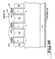
- FIGs. 1 and 2 respectively illustrate a structural diagram and a corresponding circuit diagram of an example SRAM cell arrangement, according to the present invention.
- the example arrangement shown in FIG. 1 can be referred to as a vertical storage SRAM device.
- the cell consists of two elements: a PNPN-type NDR device 10 and an NMOS-type access (or pass) transistor 12.
- the PNPN-type NDR device 10 comprises a pedestal arrangement of stacked regions with an upper end P+ region 102, an adjacent middle N region 102, an adjacent middle P region 103 and a lower most adjacent end N+ region 104.
- the access (or pass) transistor 12 includes a gate 14 that forms part of a first word-line WL1 and N+ drain and source regions in a substrate 16, with one of the N+ drain and source regions connected to a bit-line (BL) 18.
- BL bit-line
- At the top of the vertical NDR device 10 is a metalization layer 19 that is used for connecting the top terminal of the device to a supply or reference voltage, Vref.
- the NDR device 10 is made vertically on top of a portion of the access transistor 12, over the source or drain that is not connected to the bit-line 18.
- the NDR device could also be fabricated adjacent to the access transistor.
- the middle P region 103 of the NDR device 10 is adjacent to, and in a particular example embodiment surrounded by, a charge plate, or gate-like device, 20.
- the plate 20 forms part of a second word line (WL2) and is used in connection with the cells two stable states: the OFF state, where the device 10 is in a current-blocking mode; and the ON state, where the device 10 is in a current-passing mode.
- the voltage of the storage node 24 is at its high value for the ON state, and the holding current of the NDR device is provided by the sub-threshold current of the access transistor 12.
- FIG. 2 also shows a resistor 26 for an alternative embodiment, the resistor 26 being used to help maintain the holding current for the NDR device in its ON state.
- the resistor 26 is advantageous in that it may provide better controllability for the standby current in the cell.
- the plate 20 overlaps the lower N+ region 104 but not the upper N region 102.
- the PNPN device is sufficiently thin so that the gate has tight control on the potential of the P region 103 of the PNPN and this potential can be modulated by the capacitive coupling via the plate 20.
- the lower N+ region 104 is the internal node of the cell and corresponds to the storage node 24 of FIG. 2.
- the upper P+ region 101 is connected to a reference voltage.
- WL2 is used for write operations and, more particularly, to speed up the device 10 turn-off when writing a logical zero to the cell and to enable the device 10 to turn-on at low voltages when writing a logical one to the cell. In standby mode, the word-lines and the bit-line are inactive or at their low voltage levels (which can be different for each line).
- FIGs. 3a and 3b respectively illustrate DC and AC circuit models of the example arrangement of FIG. 1, shown using bipolar-junction transistors 10a and 10b.
- WL2 is shown capacitively coupled to the NDR device 10 at the P region to enhance, and thereby speed up, the switching of current between the terminals of me NDR device.
- the adjacent gate (20 of FIG. 1) is modeled as a vertical MOSFET 26 connecting the base of the PNP transistor 10a to the bit-line (BL) via the pass transistor.
- the equivalent circuit model of the cell is shown in FIG. 3b, simplified to a capacitive coupling between WL2 and the P region of the PNPN.
- FIG. 4 is a timing diagram showing waveforms of various nodes of the circuit of FIG. 1, according to another aspect of the present invention.
- the diagram shows example read and write operations for this cell.
- WL1 is used to read the voltage of the storage node 24.
- the bit line stays low.
- a pulse is applied to WL2.
- the rising edge of this pulse raises the potential of the P region by capacitive coupling and makes the NP and lower PN junctions forward biased which, in-turn, starts the well-known regenerative process in the PNPN and turns the NDR device on.
- BL is raised to its high level and WL1 becomes active. This charges the level at the storage node to a high voltage level and causes the NDR device to become reverse biased.
- a pulse is then applied to WL2. The falling edge of this pulse pulls out all the minority charges from the middle P region of the PNPN and blocks the current pass. In this embodiment, this is done only when the PNPN device is "thin”. The PNPN is switched to the blocking state after this operation. This turn-off operation does not depend on the normal turn-off mechanism in a multiple PN device (recombination of the minority charges inside the device) and therefore is fast and reliable.
- FIG. 5 is an example layout arrangement of the structure of FIG. 1, according to another aspect of the present invention.
- An important advantage of the structure of FIG. 1 is its considerably smaller cell area compared to conventional SRAM cells. This layout and structure can be implemented to consume a reasonable level of standby power, and to provide insensitivity to varying voltage levels, good noise margins and high speed.
- the structure of FIG. 5 is similar to conventional DRAMs in terms of architecture, speed, and the fabrication process. Further, in terms of the circuit real estate, the footprint of the cell shown in FIG. 5 is as small as the footprint of many conventional DRAM cells.
- the fabrication of this cell structure can be based on CMOS technology with an additional epitaxial growth step to build the PNPN device, and this process can be similar to conventional stacked capacitor cells with the capacitance being replaced by the NDR device.
- the spacing between the bottom of each gate and the top of the NDR device is adjusted by a timed over-etch of the deposited poly.
- the gate adjacent to the PNPN device can be readily fabricated using well-known methods, including sidewall spacer or selective epitaxy methods.
- the gate(s) adjacent to the PNPN device is (are) fabricated using an anisotropic poly etch.
- the NDR device can be fabricated either before the planar device by etching silicon pillars and ion-implantation or after the planar device, for example, by selective epitaxial growth techniques.
- FIG. 6 illustrates an alternative implementation to that which is shown in FIG. 1.
- the structures of FIGs. 1 and 6 differ in that the structure of FIG. 6 includes a vertically-arranged NMOSFET 30 instead of the NMOSFET 12 of FIG. 1, which is arranged in a planar manner relative to the P substrate.
- the NMOSFET 30 includes a gate 14' that at least partially surrounds the P region of the body of the NMOSFET 30.
- the read and write operations for this embodiment are as shown in FIG. 4.
- the embodiment of FIG. 6 can be implemented in a smaller area using a more involved fabrication process.
- the gate for each of the structures of FIGs. 1 and 6 are adjacent to, and of sufficient size relative to, the facing region of the NDR device, so that the charge at the gate controls the potential across the entire diameter ("d") of the subject region of the NDR device. Accordingly, this result is realized by selecting the thickness (as exemplified by "d") of the NDR device along with the size and proximity of the gate to facing region, as well as the doping concentration of the facing region of the NDR device.
- the gate only partially surrounds the facing region of the NDR device and the NDR device has a reduced thickness to offset the reduced capacitive coupling provided by the non-surrounding gate.
- FIG. 6a shows an example embodiment of a non-surrounding gate NDR device according to present invention in an SRAM cell arrangement similar to FIG. 1.
- Thin film SOI (Silicon on Insulator) technology is employed and the PNPN-type NDR device has a planar structure rather than the vertical structure in FIG. 1.
- the read and write operations for this embodiment are as shown in FIG. 4.
- the NDR device can be implemented using any of a variety of shapes.
- a specific example embodiment uses a supply voltage of 1 volt, with each gate being N+ doped and with an oxide layer having a thickness of 200A.
- the dimensions of this example SRAM structure are shown-in FIG. 7.
- the surrounding gate 20" (WL2) overlaps with the N region of the internal storage node 24, but not with the upper N region.
- the NDR device 10" is relatively thin, (0.3u in this example embodiment) so that the gate has tight control on the potential of the P region of the NDR device 10" and this potential can be readily modulated by the capacitive coupling to the gate 20".
- BL and WL1 are kept at zero volts and WL2 is kept at -1V. If the PNPN device is off, the voltage level at the storage node is at zero volts.
- the voltage level at the storage node is about 0.4V to 0.5V.
- the threshold voltage of the access transistor is designed so that the holding current of the PNPN is provided by the sub-threshold current of the access transistor. This holding current can be as low as pico-amps per um 2 .
- the read and write operations are generally as described in connection with FIG. 4, with the upper voltage levels for WL1 at 3 volts, for BL at 2V, and for WL2 (or gate) being 2 volts.
- a 1-Gigabit SRAM includes cells implemented consistent with the above two-element NDR-based structure (of either FIG. 1, FIG. 6 or FIG. 6a) and is implemented using 0.2 ⁇ m technology with standby current operating at less than 10mA.
- Conventional logic circuitry (not shown) is used to control the timing and levels of the access signals (the word and bit lines).
- FIG. 8 is a power thryristor structure, according to another example embodiment of the present invention, having a common anode 36 and a common cathode 38 as its connecting terminals.
- the respective anodes of these devices are implemented using a metalization layer 42 interconnected by a conductor 44.
- the structure includes a plurality of PNPN-type NDR devices, three of which are depicted as 40a, 40b and 40c and each sandwiched between the common anode 36 and cathode 38.
- These NDR devices can be cells, stripes or different combinations of cells and/or stripes in the top view layout.
- Each of the plurality of PNPN-type NDR devices is constructed in a manner similar to the structure of FIG.
Landscapes
- Engineering & Computer Science (AREA)
- Power Engineering (AREA)
- Microelectronics & Electronic Packaging (AREA)
- Computer Hardware Design (AREA)
- Condensed Matter Physics & Semiconductors (AREA)
- General Physics & Mathematics (AREA)
- Physics & Mathematics (AREA)
- Ceramic Engineering (AREA)
- Static Random-Access Memory (AREA)
- Semiconductor Memories (AREA)
- Thyristors (AREA)
- Amplifiers (AREA)
- Measurement Of Current Or Voltage (AREA)
- Testing Or Measuring Of Semiconductors Or The Like (AREA)
Claims (15)
- Dispositif à semi-conducteurs, comprenant :caractérisé en ce que ladite une région (103) a une section adaptée de sorte que le couplage capacitif d'au moins une transition de tension du port de commande (20) vers ladite une région (103) commute le dispositif à lecture non destructive au moins d'un mode de passage de courant vers un mode de blocage de courant indépendamment de toute formation de canal d'inversion MOS contre ladite une région et pour le courant entre les régions d'extrémité.un dispositif à lecture non destructive (10) comportant un ensemble de régions adjacentes (101, 102, 103, 104), l'ensemble comprenant des régions de polarités opposées et des régions d'extrémité (101, 104) ; etun port de commande (20) situé adjacent, couplé de manière capacitive et faisant face à au moins l'une (103) des régions du dispositif à lecture non destructive,
- Dispositif à semi-conducteurs selon la revendication 1, dans lequel ladite au moins une transition de tension du port de commande (20) vers ladite une région (103) résulte en une sortie des porteurs minoritaires de ladite une région et commute le dispositif à lecture non destructive au moins d'un mode de passage de courant vers un mode de blocage de courant pour le courant entre les régions d'extrémité.
- Dispositif à semi-conducteurs selon la revendication 1 ou 2, dans lequel le port de commande et le dispositif à lecture non destructive sont, en outre, configurés et agencés de sorte que, en réponse à au moins une transition de tension présentée au port de commande, le potentiel d'un côté à l'autre d'une majeure partie de la section change.
- Dispositif à semi-conducteurs selon la revendication 1 ou 2, comprenant en outre au moins un autre dispositif à lecture non destructive comportant au moins deux régions contiguës de polarités opposées ;
et un autre port de commande situé adjacent et faisant face à au moins l'une des régions dudit autre dispositif à lecture non destructive. - Dispositif à semi-conducteurs selon la revendication 1 ou 2, dans lequel le couplage capacitif d'au moins une première transition de tension du port de commande vers ladite une région améliore la commutation du dispositif à lecture non destructive d'un mode de passage de courant vers un mode de blocage de courant.
- Dispositif à semi-conducteurs selon la revendication 5, dans lequel le couplage capacitif d'au moins une deuxième transition de tension du port de commande vers ladite région améliore la commutation du dispositif à lecture non destructive d'un mode de blocage de courant vers un mode de passage de courant.
- Réseau de cellules de mémoire comprenant au moins un dispositif à semi-conducteurs de l'une quelconque des revendications 1 à 6.
- Réseau de cellules de mémoire, comprenant un circuit de données configuré et agencé pour fournir des données pour écriture et lecture dans une ou plusieurs cellules sélectionnées dans le réseau, chaque cellule comportant un noeud de mémorisation (24), et comprenant un dispositif à semi-conducteurs selon l'une quelconque des revendications 1 à 6, le dispositif à semi-conducteurs étant, en outre, caractérisé par un circuit d'accès (12) configuré et agencé pour coupler des données entre le noeud de mémorisation et le circuit de données.
- Réseau de cellules de mémoire selon la revendication 8, comprenant une première ligne de mot, une deuxième ligne de mot, le dispositif à semi-conducteurs étant, en outre, caractérisé en ce que le port de commande est adapté pour réagir à des transitions de tension présentées par la deuxième ligne de mot, et en ce que le circuit d'accès a une porte d'accès couplée à la première ligne de mot et configurée et agencée pour coupler des données entre le noeud de mémorisation et une ligne de bit.
- Dispositif à semi-conducteurs selon l'une quelconque des revendications 1 à 7, dans lequel au moins le dispositif à lecture non destructive est configuré et agencé dans un socle (10') et s'étend au-dessus ou au-dessous d'un substrat, le port de commande couplé de manière capacitive (20') entourant au moins une partie du socle.
- Réseau de cellules de mémoire selon la revendication 8 ou 9, comprenant en outre un circuit d'attente adapté pour fournir un courant d'attente pour le noeud de mémorisation.
- Dispositif à semi-conducteurs selon l'une quelconque des revendications 1 à 7, comprenant en outre une couche de matériau isolant en tant que partie d'une structure silicium sur isolant, dans lequel au moins le dispositif à lecture non destructive est situé adjacent au matériau isolant.
- Dispositif à semi-conducteurs selon l'une quelconque des revendications 1 à 7, dans lequel le port de commande et le dispositif à lecture non destructive sont, en outre, adaptés en tant que partie d'un commutateur de puissance à semi-conducteurs.
- Dispositif à semi-conducteurs selon la revendication 1 ou 2, dans lequel le dispositif à lecture non destructive (10) et le port de commande (20) font partie d'une cellule de mémoire dans laquelle le port de commande (20) est adapté pour réagir à une ligne de mot (14) et le dispositif à lecture non destructive (10) est adapté pour fournir deux états stables pour la cellule de mémoire.
- Procédé de commutation de courant à travers des régions contiguës d'un dispositif à lecture non destructive dans un dispositif à semi-conducteurs, le dispositif à lecture non destructive (10) ayant un port de commande couplé de manière capacitive et faisant face à au moins l'une des régions et ayant également un mode de blocage de courant et un mode de passage de courant, le procédé comprenant :le couplage capacitif d'au moins un front d'une première impulsion de tension du port de commande vers ladite au moins une des régions pour commuter le dispositif à lecture non destructive d'un mode de passage de courant vers un mode de blocage de courant ; etle couplage capacitif d'au moins un front d'une deuxième impulsion de tension du port de commande vers ladite au moins une des régions pour commuter le dispositif à lecture non destructive d'un mode de blocage de courant vers un mode de passage de courant, chacune des première et deuxième impulsions de tension ayant une polarité commune.
Applications Claiming Priority (3)
| Application Number | Priority Date | Filing Date | Title |
|---|---|---|---|
| US92449 | 1998-06-05 | ||
| US09/092,449 US6229161B1 (en) | 1998-06-05 | 1998-06-05 | Semiconductor capacitively-coupled NDR device and its applications in high-density high-speed memories and in power switches |
| PCT/US1999/012481 WO1999063598A1 (fr) | 1998-06-05 | 1999-06-01 | Dispositif de commutation de courant de semi-conducteur possedant un dispositif d'amelioration operationnel et procede correspond |
Publications (2)
| Publication Number | Publication Date |
|---|---|
| EP1082764A1 EP1082764A1 (fr) | 2001-03-14 |
| EP1082764B1 true EP1082764B1 (fr) | 2004-02-11 |
Family
ID=22233267
Family Applications (1)
| Application Number | Title | Priority Date | Filing Date |
|---|---|---|---|
| EP99930143A Expired - Lifetime EP1082764B1 (fr) | 1998-06-05 | 1999-06-01 | Dispositif de commutation de courant de semi-conducteur possedant un dispositif d'amelioration operationnel et procede correspond |
Country Status (7)
| Country | Link |
|---|---|
| US (7) | US6229161B1 (fr) |
| EP (1) | EP1082764B1 (fr) |
| JP (1) | JP4763889B2 (fr) |
| KR (1) | KR100636777B1 (fr) |
| AT (1) | ATE259545T1 (fr) |
| DE (1) | DE69914746T2 (fr) |
| WO (1) | WO1999063598A1 (fr) |
Families Citing this family (451)
| Publication number | Priority date | Publication date | Assignee | Title |
|---|---|---|---|---|
| US7203728B2 (en) * | 1993-01-26 | 2007-04-10 | Logic Controls, Inc. | Point-of-sale system and distributed computer network for same |
| US8018058B2 (en) * | 2004-06-21 | 2011-09-13 | Besang Inc. | Semiconductor memory device |
| US7633162B2 (en) * | 2004-06-21 | 2009-12-15 | Sang-Yun Lee | Electronic circuit with embedded memory |
| US7800199B2 (en) * | 2003-06-24 | 2010-09-21 | Oh Choonsik | Semiconductor circuit |
| US20050280155A1 (en) * | 2004-06-21 | 2005-12-22 | Sang-Yun Lee | Semiconductor bonding and layer transfer method |
| US8058142B2 (en) | 1996-11-04 | 2011-11-15 | Besang Inc. | Bonded semiconductor structure and method of making the same |
| US6890546B2 (en) | 1998-09-24 | 2005-05-10 | Abbott Laboratories | Medical devices containing rapamycin analogs |
| US20030129215A1 (en) * | 1998-09-24 | 2003-07-10 | T-Ram, Inc. | Medical devices containing rapamycin analogs |
| US6229161B1 (en) * | 1998-06-05 | 2001-05-08 | Stanford University | Semiconductor capacitively-coupled NDR device and its applications in high-density high-speed memories and in power switches |
| US6891213B1 (en) | 1999-03-16 | 2005-05-10 | Micron Technology, Inc. | Base current reversal SRAM memory cell and method |
| US6313490B1 (en) * | 1999-03-16 | 2001-11-06 | Micron Technology, Inc. | Base current reversal SRAM memory cell and method |
| US6690038B1 (en) * | 1999-06-05 | 2004-02-10 | T-Ram, Inc. | Thyristor-based device over substrate surface |
| FI108889B (fi) * | 2000-04-27 | 2002-04-15 | Jukka Pekola | Menetelmä lämpötilan mittaamiseksi laajalla alueella tunneliliitosta hyväksikäyttäen |
| US6518589B2 (en) | 2000-06-22 | 2003-02-11 | Progressant Technologies, Inc. | Dual mode FET & logic circuit having negative differential resistance mode |
| US6596617B1 (en) | 2000-06-22 | 2003-07-22 | Progressant Technologies, Inc. | CMOS compatible process for making a tunable negative differential resistance (NDR) device |
| US6479862B1 (en) | 2000-06-22 | 2002-11-12 | Progressant Technologies, Inc. | Charge trapping device and method for implementing a transistor having a negative differential resistance mode |
| US6594193B2 (en) | 2000-06-22 | 2003-07-15 | Progressent Technologies, Inc. | Charge pump for negative differential resistance transistor |
| US6559470B2 (en) | 2000-06-22 | 2003-05-06 | Progressed Technologies, Inc. | Negative differential resistance field effect transistor (NDR-FET) and circuits using the same |
| US6754104B2 (en) | 2000-06-22 | 2004-06-22 | Progressant Technologies, Inc. | Insulated-gate field-effect transistor integrated with negative differential resistance (NDR) FET |
| US6724655B2 (en) | 2000-06-22 | 2004-04-20 | Progressant Technologies, Inc. | Memory cell using negative differential resistance field effect transistors |
| US6512274B1 (en) | 2000-06-22 | 2003-01-28 | Progressant Technologies, Inc. | CMOS-process compatible, tunable NDR (negative differential resistance) device and method of operating same |
| JP4044276B2 (ja) * | 2000-09-28 | 2008-02-06 | 株式会社東芝 | 半導体装置及びその製造方法 |
| US6549450B1 (en) * | 2000-11-08 | 2003-04-15 | Ibm Corporation | Method and system for improving the performance on SOI memory arrays in an SRAM architecture system |
| US6713791B2 (en) * | 2001-01-26 | 2004-03-30 | Ibm Corporation | T-RAM array having a planar cell structure and method for fabricating the same |
| US7075122B1 (en) | 2001-03-22 | 2006-07-11 | T-Ram Semiconductor, Inc. | Thyristor device with carbon lifetime adjustment implant and its method of fabrication |
| US7374974B1 (en) | 2001-03-22 | 2008-05-20 | T-Ram Semiconductor, Inc. | Thyristor-based device with trench dielectric material |
| US7491586B2 (en) * | 2001-03-22 | 2009-02-17 | T-Ram Semiconductor, Inc. | Semiconductor device with leakage implant and method of fabrication |
| US6727528B1 (en) | 2001-03-22 | 2004-04-27 | T-Ram, Inc. | Thyristor-based device including trench dielectric isolation for thyristor-body regions |
| US6462359B1 (en) * | 2001-03-22 | 2002-10-08 | T-Ram, Inc. | Stability in thyristor-based memory device |
| US6891205B1 (en) | 2001-03-22 | 2005-05-10 | T-Ram, Inc. | Stability in thyristor-based memory device |
| US7456439B1 (en) * | 2001-03-22 | 2008-11-25 | T-Ram Semiconductor, Inc. | Vertical thyristor-based memory with trench isolation and its method of fabrication |
| US6804162B1 (en) | 2001-04-05 | 2004-10-12 | T-Ram, Inc. | Read-modify-write memory using read-or-write banks |
| US6885581B2 (en) * | 2001-04-05 | 2005-04-26 | T-Ram, Inc. | Dynamic data restore in thyristor-based memory device |
| US6627924B2 (en) * | 2001-04-30 | 2003-09-30 | Ibm Corporation | Memory system capable of operating at high temperatures and method for fabricating the same |
| DE10125967C1 (de) * | 2001-05-29 | 2002-07-11 | Infineon Technologies Ag | DRAM-Zellanordnung mit vertikalen MOS-Transistoren und Verfahren zu deren Herstellung |
| US6906354B2 (en) * | 2001-06-13 | 2005-06-14 | International Business Machines Corporation | T-RAM cell having a buried vertical thyristor and a pseudo-TFT transfer gate and method for fabricating the same |
| US6583452B1 (en) | 2001-12-17 | 2003-06-24 | T-Ram, Inc. | Thyristor-based device having extended capacitive coupling |
| US7453083B2 (en) | 2001-12-21 | 2008-11-18 | Synopsys, Inc. | Negative differential resistance field effect transistor for implementing a pull up element in a memory cell |
| US6670642B2 (en) * | 2002-01-22 | 2003-12-30 | Renesas Technology Corporation. | Semiconductor memory device using vertical-channel transistors |
| WO2003065418A2 (fr) * | 2002-02-01 | 2003-08-07 | Picometrix, Inc. | Photodiode a avalanche planaire |
| ES2616248T3 (es) * | 2002-02-01 | 2017-06-12 | Picometrix, Llc | Fotodiodo PIN de alta velocidad con respuesta incrementada |
| CN1633699A (zh) * | 2002-02-01 | 2005-06-29 | 派克米瑞斯公司 | 电荷控制雪崩光电二极管及其制造方法 |
| US7294567B2 (en) * | 2002-03-11 | 2007-11-13 | Micron Technology, Inc. | Semiconductor contact device and method |
| US6940772B1 (en) | 2002-03-18 | 2005-09-06 | T-Ram, Inc | Reference cells for TCCT based memory cells |
| US7123508B1 (en) | 2002-03-18 | 2006-10-17 | T-Ram, Inc. | Reference cells for TCCT based memory cells |
| US6832300B2 (en) | 2002-03-20 | 2004-12-14 | Hewlett-Packard Development Company, L.P. | Methods and apparatus for control of asynchronous cache |
| US6785169B1 (en) | 2002-04-05 | 2004-08-31 | T-Ram, Inc. | Memory cell error recovery |
| US6611452B1 (en) | 2002-04-05 | 2003-08-26 | T-Ram, Inc. | Reference cells for TCCT based memory cells |
| US6778435B1 (en) | 2002-06-12 | 2004-08-17 | T-Ram, Inc. | Memory architecture for TCCT-based memory cells |
| JP3660650B2 (ja) * | 2002-06-13 | 2005-06-15 | 株式会社東芝 | 半導体装置の製造方法 |
| US20060113612A1 (en) * | 2002-06-19 | 2006-06-01 | Kailash Gopalakrishnan | Insulated-gate semiconductor device and approach involving junction-induced intermediate region |
| US6567292B1 (en) | 2002-06-28 | 2003-05-20 | Progressant Technologies, Inc. | Negative differential resistance (NDR) element and memory with reduced soft error rate |
| US6795337B2 (en) | 2002-06-28 | 2004-09-21 | Progressant Technologies, Inc. | Negative differential resistance (NDR) elements and memory device using the same |
| US6721220B2 (en) * | 2002-07-05 | 2004-04-13 | T-Ram, Inc. | Bit line control and sense amplification for TCCT-based memory cells |
| US7221586B2 (en) | 2002-07-08 | 2007-05-22 | Micron Technology, Inc. | Memory utilizing oxide nanolaminates |
| US6865407B2 (en) * | 2002-07-11 | 2005-03-08 | Optical Sensors, Inc. | Calibration technique for non-invasive medical devices |
| US6903969B2 (en) * | 2002-08-30 | 2005-06-07 | Micron Technology Inc. | One-device non-volatile random access memory cell |
| US6917078B2 (en) | 2002-08-30 | 2005-07-12 | Micron Technology Inc. | One transistor SOI non-volatile random access memory cell |
| US6888200B2 (en) * | 2002-08-30 | 2005-05-03 | Micron Technology Inc. | One transistor SOI non-volatile random access memory cell |
| US7042027B2 (en) * | 2002-08-30 | 2006-05-09 | Micron Technology, Inc. | Gated lateral thyristor-based random access memory cell (GLTRAM) |
| US7135745B1 (en) | 2002-09-09 | 2006-11-14 | T-Ram, Inc. | Fin thyristor-based semiconductor device |
| US6790713B1 (en) | 2002-09-09 | 2004-09-14 | T-Ram, Inc. | Method for making an inlayed thyristor-based device |
| US7053423B1 (en) | 2002-09-24 | 2006-05-30 | T-Ram, Inc. | Thyristor having a first emitter with relatively lightly doped portion to the base |
| US6888177B1 (en) | 2002-09-24 | 2005-05-03 | T-Ram, Inc. | Increased base-emitter capacitance |
| US6703646B1 (en) | 2002-09-24 | 2004-03-09 | T-Ram, Inc. | Thyristor with lightly-doped emitter |
| US6828202B1 (en) * | 2002-10-01 | 2004-12-07 | T-Ram, Inc. | Semiconductor region self-aligned with ion implant shadowing |
| US6818482B1 (en) | 2002-10-01 | 2004-11-16 | T-Ram, Inc. | Method for trench isolation for thyristor-based device |
| US6767770B1 (en) | 2002-10-01 | 2004-07-27 | T-Ram, Inc. | Method of forming self-aligned thin capacitively-coupled thyristor structure |
| US7279367B1 (en) | 2004-12-07 | 2007-10-09 | T-Ram Semiconductor, Inc. | Method of manufacturing a thyristor semiconductor device |
| US6683330B1 (en) * | 2002-10-01 | 2004-01-27 | T-Ram, Inc. | Recessed thyristor control port |
| US7125753B1 (en) | 2002-10-01 | 2006-10-24 | T-Ram Semiconductor, Inc. | Self-aligned thin capacitively-coupled thyristor structure |
| US6690039B1 (en) | 2002-10-01 | 2004-02-10 | T-Ram, Inc. | Thyristor-based device that inhibits undesirable conductive channel formation |
| US7030425B1 (en) | 2002-10-01 | 2006-04-18 | Tram, Inc. | Buried emitter contact for thyristor-based semiconductor device |
| US6953953B1 (en) | 2002-10-01 | 2005-10-11 | T-Ram, Inc. | Deep trench isolation for thyristor-based semiconductor device |
| US6815734B1 (en) | 2002-10-01 | 2004-11-09 | T-Ram, Inc. | Varied trench depth for thyristor isolation |
| US6913955B1 (en) | 2002-10-01 | 2005-07-05 | T-Ram, Inc. | Method of manufacturing a thyristor device with a control port in a trench |
| US6998652B1 (en) | 2002-10-01 | 2006-02-14 | T-Ram, Inc. | Trench isolation for thyristor-based device |
| US6888176B1 (en) | 2002-10-01 | 2005-05-03 | T-Ram, Inc. | Thyrister semiconductor device |
| US6666481B1 (en) | 2002-10-01 | 2003-12-23 | T-Ram, Inc. | Shunt connection to emitter |
| US6686612B1 (en) | 2002-10-01 | 2004-02-03 | T-Ram, Inc. | Thyristor-based device adapted to inhibit parasitic current |
| US6735113B2 (en) * | 2002-10-15 | 2004-05-11 | T-Ram, Inc. | Circuit and method for implementing a write operation with TCCT-based memory cells |
| US6756612B1 (en) | 2002-10-28 | 2004-06-29 | T-Ram, Inc. | Carrier coupler for thyristor-based semiconductor device |
| US6965129B1 (en) | 2002-11-06 | 2005-11-15 | T-Ram, Inc. | Thyristor-based device having dual control ports |
| US6980457B1 (en) | 2002-11-06 | 2005-12-27 | T-Ram, Inc. | Thyristor-based device having a reduced-resistance contact to a buried emitter region |
| US6812084B2 (en) | 2002-12-09 | 2004-11-02 | Progressant Technologies, Inc. | Adaptive negative differential resistance device |
| US6806117B2 (en) | 2002-12-09 | 2004-10-19 | Progressant Technologies, Inc. | Methods of testing/stressing a charge trapping device |
| US7005711B2 (en) | 2002-12-20 | 2006-02-28 | Progressant Technologies, Inc. | N-channel pull-up element and logic circuit |
| US7799675B2 (en) * | 2003-06-24 | 2010-09-21 | Sang-Yun Lee | Bonded semiconductor structure and method of fabricating the same |
| US20100133695A1 (en) * | 2003-01-12 | 2010-06-03 | Sang-Yun Lee | Electronic circuit with embedded memory |
| US6812504B2 (en) * | 2003-02-10 | 2004-11-02 | Micron Technology, Inc. | TFT-based random access memory cells comprising thyristors |
| US6756838B1 (en) | 2003-03-18 | 2004-06-29 | T-Ram, Inc. | Charge pump based voltage regulator with smart power regulation |
| US6845026B1 (en) | 2003-05-30 | 2005-01-18 | Netlogic Microsystems, Inc. | Thyristor-based content addressable memory (CAM) cells |
| CN1326250C (zh) * | 2003-06-17 | 2007-07-11 | 台湾积体电路制造股份有限公司 | 绝缘硅芯片的鳍状元件及其形成方法 |
| US8071438B2 (en) * | 2003-06-24 | 2011-12-06 | Besang Inc. | Semiconductor circuit |
| US20100190334A1 (en) * | 2003-06-24 | 2010-07-29 | Sang-Yun Lee | Three-dimensional semiconductor structure and method of manufacturing the same |
| US7867822B2 (en) | 2003-06-24 | 2011-01-11 | Sang-Yun Lee | Semiconductor memory device |
| US20040263316A1 (en) * | 2003-06-24 | 2004-12-30 | Case, Llc | Reprogrammable vehicle access control system |
| US7863748B2 (en) * | 2003-06-24 | 2011-01-04 | Oh Choonsik | Semiconductor circuit and method of fabricating the same |
| US7632738B2 (en) * | 2003-06-24 | 2009-12-15 | Sang-Yun Lee | Wafer bonding method |
| US8471263B2 (en) * | 2003-06-24 | 2013-06-25 | Sang-Yun Lee | Information storage system which includes a bonded semiconductor structure |
| US20060231857A1 (en) * | 2003-06-26 | 2006-10-19 | Rj Mears, Llc | Method for making a semiconductor device including a memory cell with a negative differential resistance (ndr) device |
| US7531850B2 (en) * | 2003-06-26 | 2009-05-12 | Mears Technologies, Inc. | Semiconductor device including a memory cell with a negative differential resistance (NDR) device |
| US8125003B2 (en) * | 2003-07-02 | 2012-02-28 | Micron Technology, Inc. | High-performance one-transistor memory cell |
| US6849481B1 (en) * | 2003-07-28 | 2005-02-01 | Chartered Semiconductor Manufacturing Ltd. | Thyristor-based SRAM and method for the fabrication thereof |
| US6897111B2 (en) * | 2003-07-28 | 2005-05-24 | Chartered Semiconductor Manufacturing Ltd. | Method using quasi-planar double gated fin field effect transistor process for the fabrication of a thyristor-based static read/write random-access memory |
| US6998298B1 (en) | 2003-08-11 | 2006-02-14 | T-Ram Semiconductor, Inc. | Thyristor semiconductor memory device and method of manufacture |
| US7089439B1 (en) | 2003-09-03 | 2006-08-08 | T-Ram, Inc. | Architecture and method for output clock generation on a high speed memory device |
| US7464282B1 (en) | 2003-09-03 | 2008-12-09 | T-Ram Semiconductor, Inc. | Apparatus and method for producing dummy data and output clock generator using same |
| US6891774B1 (en) | 2003-09-03 | 2005-05-10 | T-Ram, Inc. | Delay line and output clock generator using same |
| US6947349B1 (en) | 2003-09-03 | 2005-09-20 | T-Ram, Inc. | Apparatus and method for producing an output clock pulse and output clock generator using same |
| US7195959B1 (en) | 2004-10-04 | 2007-03-27 | T-Ram Semiconductor, Inc. | Thyristor-based semiconductor device and method of fabrication |
| US7592642B1 (en) | 2003-09-25 | 2009-09-22 | T-Ram Semiconductor, Inc. | Thyristor-based semiconductor device with indium-carbon implant and method of fabrication |
| US6944051B1 (en) | 2003-10-29 | 2005-09-13 | T-Ram, Inc. | Data restore in thryistor based memory devices |
| US7304327B1 (en) | 2003-11-12 | 2007-12-04 | T-Ram Semiconductor, Inc. | Thyristor circuit and approach for temperature stability |
| US7268373B1 (en) | 2003-11-12 | 2007-09-11 | T-Ram Semiconductor, Inc. | Thyristor-based memory and its method of operation |
| US7109532B1 (en) | 2003-12-23 | 2006-09-19 | Lee Zachary K | High Ion/Ioff SOI MOSFET using body voltage control |
| US7081378B2 (en) * | 2004-01-05 | 2006-07-25 | Chartered Semiconductor Manufacturing Ltd. | Horizontal TRAM and method for the fabrication thereof |
| US8253195B2 (en) | 2004-01-29 | 2012-08-28 | Enpirion, Inc. | Integrated circuit with a laterally diffused metal oxide semiconductor device and method of forming the same |
| US8253196B2 (en) | 2004-01-29 | 2012-08-28 | Enpirion, Inc. | Integrated circuit with a laterally diffused metal oxide semiconductor device and method of forming the same |
| US8212317B2 (en) | 2004-01-29 | 2012-07-03 | Enpirion, Inc. | Integrated circuit with a laterally diffused metal oxide semiconductor device and method of forming the same |
| US8253197B2 (en) | 2004-01-29 | 2012-08-28 | Enpirion, Inc. | Integrated circuit with a laterally diffused metal oxide semiconductor device and method of forming the same |
| US8212315B2 (en) | 2004-01-29 | 2012-07-03 | Enpirion, Inc. | Integrated circuit with a laterally diffused metal oxide semiconductor device and method of forming the same |
| US7230302B2 (en) * | 2004-01-29 | 2007-06-12 | Enpirion, Inc. | Laterally diffused metal oxide semiconductor device and method of forming the same |
| US8212316B2 (en) | 2004-01-29 | 2012-07-03 | Enpirion, Inc. | Integrated circuit with a laterally diffused metal oxide semiconductor device and method of forming the same |
| KR100527559B1 (ko) * | 2004-02-05 | 2005-11-09 | 주식회사 하이닉스반도체 | 직렬 다이오드 셀을 이용한 불휘발성 메모리 장치 |
| KR100694426B1 (ko) * | 2004-02-16 | 2007-03-12 | 주식회사 하이닉스반도체 | 나노 튜브 셀 및 이를 이용한 메모리 장치 |
| KR100709462B1 (ko) * | 2004-02-16 | 2007-04-18 | 주식회사 하이닉스반도체 | 다층 나노 튜브 셀을 이용한 메모리 장치 |
| KR100709463B1 (ko) * | 2004-02-16 | 2007-04-18 | 주식회사 하이닉스반도체 | 나노 튜브 셀을 이용한 메모리 장치 |
| US7224002B2 (en) * | 2004-05-06 | 2007-05-29 | Micron Technology, Inc. | Silicon on insulator read-write non-volatile memory comprising lateral thyristor and trapping layer |
| US7054191B1 (en) | 2004-06-03 | 2006-05-30 | T-Ram, Inc. | Method and system for writing data to memory cells |
| US7229886B2 (en) * | 2004-08-23 | 2007-06-12 | Enpirion, Inc. | Method of forming an integrated circuit incorporating higher voltage devices and low voltage devices therein |
| US7232733B2 (en) * | 2004-08-23 | 2007-06-19 | Enpirion, Inc. | Method of forming an integrated circuit incorporating higher voltage devices and low voltage devices therein |
| US7195981B2 (en) * | 2004-08-23 | 2007-03-27 | Enpirion, Inc. | Method of forming an integrated circuit employable with a power converter |
| US7335948B2 (en) * | 2004-08-23 | 2008-02-26 | Enpirion, Inc. | Integrated circuit incorporating higher voltage devices and low voltage devices therein |
| US7190026B2 (en) * | 2004-08-23 | 2007-03-13 | Enpirion, Inc. | Integrated circuit employable with a power converter |
| US7145186B2 (en) * | 2004-08-24 | 2006-12-05 | Micron Technology, Inc. | Memory cell with trenched gated thyristor |
| US7326969B1 (en) | 2004-12-02 | 2008-02-05 | T-Ram Semiconductor, Inc. | Semiconductor device incorporating thyristor-based memory and strained silicon |
| US8367524B2 (en) * | 2005-03-29 | 2013-02-05 | Sang-Yun Lee | Three-dimensional integrated circuit structure |
| US20110143506A1 (en) * | 2009-12-10 | 2011-06-16 | Sang-Yun Lee | Method for fabricating a semiconductor memory device |
| US8455978B2 (en) | 2010-05-27 | 2013-06-04 | Sang-Yun Lee | Semiconductor circuit structure and method of making the same |
| US7573077B1 (en) | 2005-05-04 | 2009-08-11 | T-Ram Semiconductor, Inc. | Thyristor-based semiconductor memory device with back-gate bias |
| US8093107B1 (en) | 2005-06-22 | 2012-01-10 | T-Ram Semiconductor, Inc. | Thyristor semiconductor memory and method of manufacture |
| US7894255B1 (en) | 2005-06-22 | 2011-02-22 | T-Ram Semiconductor, Inc. | Thyristor based memory cell |
| US7460395B1 (en) | 2005-06-22 | 2008-12-02 | T-Ram Semiconductor, Inc. | Thyristor-based semiconductor memory and memory array with data refresh |
| US7894256B1 (en) | 2005-06-22 | 2011-02-22 | T-Ram Semiconductor, Inc. | Thyristor based memory cell |
| US7379381B1 (en) | 2005-07-05 | 2008-05-27 | T-Ram Semiconductor, Inc. | State maintenance pulsing for a memory device |
| US7319622B1 (en) | 2005-07-05 | 2008-01-15 | T-Ram Semiconductor, Inc. | Bitline shielding for thyristor-based memory |
| JP4696964B2 (ja) * | 2005-07-15 | 2011-06-08 | ソニー株式会社 | メモリ用の半導体装置 |
| US7381999B1 (en) | 2005-07-21 | 2008-06-03 | T-Ram Semiconductor, Inc. | Workfunction-adjusted thyristor-based memory device |
| JP2007067133A (ja) * | 2005-08-31 | 2007-03-15 | Sony Corp | 半導体装置 |
| US7606066B2 (en) | 2005-09-07 | 2009-10-20 | Innovative Silicon Isi Sa | Memory cell and memory cell array having an electrically floating body transistor, and methods of operating same |
| US7655973B2 (en) * | 2005-10-31 | 2010-02-02 | Micron Technology, Inc. | Recessed channel negative differential resistance-based memory cell |
| US7209384B1 (en) * | 2005-12-08 | 2007-04-24 | Juhan Kim | Planar capacitor memory cell and its applications |
| US7786505B1 (en) | 2005-12-16 | 2010-08-31 | T-Ram Semiconductor, Inc. | Reduction of charge leakage from a thyristor-based memory cell |
| US20070189067A1 (en) * | 2006-02-15 | 2007-08-16 | Francis Goodwin | Dynamic memory |
| US7554130B1 (en) | 2006-02-23 | 2009-06-30 | T-Ram Semiconductor, Inc. | Reducing effects of parasitic transistors in thyristor-based memory using an isolation or damage region |
| US8174046B1 (en) | 2006-02-23 | 2012-05-08 | T-Ram Semiconductor, Inc | Reducing effects of parasitic transistors in thyristor-based memory using local thinning or implanting |
| US7425491B2 (en) * | 2006-04-04 | 2008-09-16 | Micron Technology, Inc. | Nanowire transistor with surrounding gate |
| US8734583B2 (en) * | 2006-04-04 | 2014-05-27 | Micron Technology, Inc. | Grown nanofin transistors |
| US8354311B2 (en) * | 2006-04-04 | 2013-01-15 | Micron Technology, Inc. | Method for forming nanofin transistors |
| US20070228491A1 (en) * | 2006-04-04 | 2007-10-04 | Micron Technology, Inc. | Tunneling transistor with sublithographic channel |
| US7491995B2 (en) | 2006-04-04 | 2009-02-17 | Micron Technology, Inc. | DRAM with nanofin transistors |
| US20070257326A1 (en) * | 2006-05-08 | 2007-11-08 | Chien-Li Kuo | Integrated circuit structure and method of manufacturing a memory cell |
| JP2008028353A (ja) * | 2006-06-22 | 2008-02-07 | Sony Corp | 半導体装置およびその駆動方法 |
| US7781797B2 (en) * | 2006-06-29 | 2010-08-24 | International Business Machines Corporation | One-transistor static random access memory with integrated vertical PNPN device |
| JP2008041734A (ja) * | 2006-08-02 | 2008-02-21 | Sony Corp | 半導体装置および半導体装置の製造方法 |
| US8264041B2 (en) | 2007-01-26 | 2012-09-11 | Micron Technology, Inc. | Semiconductor device with electrically floating body |
| US8518774B2 (en) | 2007-03-29 | 2013-08-27 | Micron Technology, Inc. | Manufacturing process for zero-capacitor random access memory circuits |
| JP2008263133A (ja) * | 2007-04-13 | 2008-10-30 | Toshiba Microelectronics Corp | 半導体記憶装置およびその駆動方法 |
| US8064274B2 (en) | 2007-05-30 | 2011-11-22 | Micron Technology, Inc. | Integrated circuit having voltage generation circuitry for memory cell array, and method of operating and/or controlling same |
| US8194487B2 (en) | 2007-09-17 | 2012-06-05 | Micron Technology, Inc. | Refreshing data of memory cells with electrically floating body transistors |
| JP5151370B2 (ja) * | 2007-09-28 | 2013-02-27 | ソニー株式会社 | 半導体装置 |
| US7738274B1 (en) | 2007-10-15 | 2010-06-15 | T-Ram Semiconductor, Inc. | Content-addressable memory architecture |
| US7847338B2 (en) | 2007-10-24 | 2010-12-07 | Yuniarto Widjaja | Semiconductor memory having both volatile and non-volatile functionality and method of operating |
| US8035126B2 (en) * | 2007-10-29 | 2011-10-11 | International Business Machines Corporation | One-transistor static random access memory with integrated vertical PNPN device |
| US8536628B2 (en) | 2007-11-29 | 2013-09-17 | Micron Technology, Inc. | Integrated circuit having memory cell array including barriers, and method of manufacturing same |
| US8773933B2 (en) | 2012-03-16 | 2014-07-08 | Micron Technology, Inc. | Techniques for accessing memory cells |
| WO2009110050A1 (fr) * | 2008-02-15 | 2009-09-11 | 日本ユニサンティスエレクトロニクス株式会社 | Procédé de fabrication d'un dispositif semiconducteur |
| WO2009101704A1 (fr) * | 2008-02-15 | 2009-08-20 | Unisantis Electronics (Japan) Ltd. | Procédé de fabrication d'un dispositif semiconducteur |
| WO2009110049A1 (fr) * | 2008-02-15 | 2009-09-11 | 日本ユニサンティスエレクトロニクス株式会社 | Dispositif semiconducteur et procédé pour sa fabrication |
| US7940560B2 (en) * | 2008-05-29 | 2011-05-10 | Advanced Micro Devices, Inc. | Memory cells, memory devices and integrated circuits incorporating the same |
| US7947543B2 (en) | 2008-09-25 | 2011-05-24 | Micron Technology, Inc. | Recessed gate silicon-on-insulator floating body device with self-aligned lateral isolation |
| WO2010102106A2 (fr) | 2009-03-04 | 2010-09-10 | Innovative Silicon Isi Sa | Techniques pour former un contact sur une couche de diffusion enfouie dans un dispositif mémoire à semi-conducteur |
| KR20120006516A (ko) | 2009-03-31 | 2012-01-18 | 마이크론 테크놀로지, 인크. | 반도체 메모리 디바이스를 제공하기 위한 기술들 |
| JP2010245196A (ja) * | 2009-04-02 | 2010-10-28 | Elpida Memory Inc | 半導体装置およびその製造方法 |
| US8384426B2 (en) | 2009-04-14 | 2013-02-26 | Monolithic 3D Inc. | Semiconductor device and structure |
| US9509313B2 (en) | 2009-04-14 | 2016-11-29 | Monolithic 3D Inc. | 3D semiconductor device |
| US8405420B2 (en) | 2009-04-14 | 2013-03-26 | Monolithic 3D Inc. | System comprising a semiconductor device and structure |
| US8058137B1 (en) | 2009-04-14 | 2011-11-15 | Monolithic 3D Inc. | Method for fabrication of a semiconductor device and structure |
| US9577642B2 (en) | 2009-04-14 | 2017-02-21 | Monolithic 3D Inc. | Method to form a 3D semiconductor device |
| US8395191B2 (en) | 2009-10-12 | 2013-03-12 | Monolithic 3D Inc. | Semiconductor device and structure |
| US9711407B2 (en) | 2009-04-14 | 2017-07-18 | Monolithic 3D Inc. | Method of manufacturing a three dimensional integrated circuit by transfer of a mono-crystalline layer |
| US8362482B2 (en) | 2009-04-14 | 2013-01-29 | Monolithic 3D Inc. | Semiconductor device and structure |
| US8754533B2 (en) | 2009-04-14 | 2014-06-17 | Monolithic 3D Inc. | Monolithic three-dimensional semiconductor device and structure |
| US7986042B2 (en) | 2009-04-14 | 2011-07-26 | Monolithic 3D Inc. | Method for fabrication of a semiconductor device and structure |
| US8669778B1 (en) | 2009-04-14 | 2014-03-11 | Monolithic 3D Inc. | Method for design and manufacturing of a 3D semiconductor device |
| US8378715B2 (en) | 2009-04-14 | 2013-02-19 | Monolithic 3D Inc. | Method to construct systems |
| US8427200B2 (en) | 2009-04-14 | 2013-04-23 | Monolithic 3D Inc. | 3D semiconductor device |
| US8373439B2 (en) | 2009-04-14 | 2013-02-12 | Monolithic 3D Inc. | 3D semiconductor device |
| US8362800B2 (en) | 2010-10-13 | 2013-01-29 | Monolithic 3D Inc. | 3D semiconductor device including field repairable logics |
| JP4577592B2 (ja) * | 2009-04-20 | 2010-11-10 | 日本ユニサンティスエレクトロニクス株式会社 | 半導体装置の製造方法 |
| US8139418B2 (en) | 2009-04-27 | 2012-03-20 | Micron Technology, Inc. | Techniques for controlling a direct injection semiconductor memory device |
| US8508994B2 (en) | 2009-04-30 | 2013-08-13 | Micron Technology, Inc. | Semiconductor device with floating gate and electrically floating body |
| US8498157B2 (en) | 2009-05-22 | 2013-07-30 | Micron Technology, Inc. | Techniques for providing a direct injection semiconductor memory device |
| US8537610B2 (en) | 2009-07-10 | 2013-09-17 | Micron Technology, Inc. | Techniques for providing a semiconductor memory device |
| US9076543B2 (en) | 2009-07-27 | 2015-07-07 | Micron Technology, Inc. | Techniques for providing a direct injection semiconductor memory device |
| US8017998B1 (en) | 2009-09-08 | 2011-09-13 | T-Ram Semiconductor, Inc. | Gettering contaminants for integrated circuits formed on a silicon-on-insulator structure |
| JP5524547B2 (ja) * | 2009-09-14 | 2014-06-18 | ユニサンティス エレクトロニクス シンガポール プライベート リミテッド | 半導体記憶装置 |
| US8536023B2 (en) | 2010-11-22 | 2013-09-17 | Monolithic 3D Inc. | Method of manufacturing a semiconductor device and structure |
| US10366970B2 (en) | 2009-10-12 | 2019-07-30 | Monolithic 3D Inc. | 3D semiconductor device and structure |
| US8450804B2 (en) | 2011-03-06 | 2013-05-28 | Monolithic 3D Inc. | Semiconductor device and structure for heat removal |
| US11018133B2 (en) | 2009-10-12 | 2021-05-25 | Monolithic 3D Inc. | 3D integrated circuit |
| US10354995B2 (en) | 2009-10-12 | 2019-07-16 | Monolithic 3D Inc. | Semiconductor memory device and structure |
| US8581349B1 (en) | 2011-05-02 | 2013-11-12 | Monolithic 3D Inc. | 3D memory semiconductor device and structure |
| US10157909B2 (en) | 2009-10-12 | 2018-12-18 | Monolithic 3D Inc. | 3D semiconductor device and structure |
| US9099424B1 (en) | 2012-08-10 | 2015-08-04 | Monolithic 3D Inc. | Semiconductor system, device and structure with heat removal |
| US8742476B1 (en) | 2012-11-27 | 2014-06-03 | Monolithic 3D Inc. | Semiconductor device and structure |
| US10388863B2 (en) | 2009-10-12 | 2019-08-20 | Monolithic 3D Inc. | 3D memory device and structure |
| US8476145B2 (en) | 2010-10-13 | 2013-07-02 | Monolithic 3D Inc. | Method of fabricating a semiconductor device and structure |
| US10043781B2 (en) | 2009-10-12 | 2018-08-07 | Monolithic 3D Inc. | 3D semiconductor device and structure |
| US11374118B2 (en) | 2009-10-12 | 2022-06-28 | Monolithic 3D Inc. | Method to form a 3D integrated circuit |
| US10910364B2 (en) | 2009-10-12 | 2021-02-02 | Monolitaic 3D Inc. | 3D semiconductor device |
| US8294159B2 (en) | 2009-10-12 | 2012-10-23 | Monolithic 3D Inc. | Method for fabrication of a semiconductor device and structure |
| KR101721850B1 (ko) * | 2009-11-13 | 2017-03-31 | 가부시키가이샤 한도오따이 에네루기 켄큐쇼 | 반도체 장치 |
| US8174881B2 (en) | 2009-11-24 | 2012-05-08 | Micron Technology, Inc. | Techniques for reducing disturbance in a semiconductor device |
| US8541819B1 (en) | 2010-12-09 | 2013-09-24 | Monolithic 3D Inc. | Semiconductor device and structure |
| US9099526B2 (en) | 2010-02-16 | 2015-08-04 | Monolithic 3D Inc. | Integrated circuit device and structure |
| US8026521B1 (en) | 2010-10-11 | 2011-09-27 | Monolithic 3D Inc. | Semiconductor device and structure |
| US8492886B2 (en) | 2010-02-16 | 2013-07-23 | Monolithic 3D Inc | 3D integrated circuit with logic |
| US8373230B1 (en) | 2010-10-13 | 2013-02-12 | Monolithic 3D Inc. | Method for fabrication of a semiconductor device and structure |
| US8461035B1 (en) | 2010-09-30 | 2013-06-11 | Monolithic 3D Inc. | Method for fabrication of a semiconductor device and structure |
| US8574982B2 (en) * | 2010-02-25 | 2013-11-05 | International Business Machines Corporation | Implementing eDRAM stacked FET structure |
| US9608119B2 (en) | 2010-03-02 | 2017-03-28 | Micron Technology, Inc. | Semiconductor-metal-on-insulator structures, methods of forming such structures, and semiconductor devices including such structures |
| US8513722B2 (en) | 2010-03-02 | 2013-08-20 | Micron Technology, Inc. | Floating body cell structures, devices including same, and methods for forming same |
| US8507966B2 (en) | 2010-03-02 | 2013-08-13 | Micron Technology, Inc. | Semiconductor cells, arrays, devices and systems having a buried conductive line and methods for forming the same |
| US9646869B2 (en) * | 2010-03-02 | 2017-05-09 | Micron Technology, Inc. | Semiconductor devices including a diode structure over a conductive strap and methods of forming such semiconductor devices |
| US8288795B2 (en) | 2010-03-02 | 2012-10-16 | Micron Technology, Inc. | Thyristor based memory cells, devices and systems including the same and methods for forming the same |
| US8576631B2 (en) | 2010-03-04 | 2013-11-05 | Micron Technology, Inc. | Techniques for sensing a semiconductor memory device |
| KR20130007609A (ko) | 2010-03-15 | 2013-01-18 | 마이크론 테크놀로지, 인크. | 반도체 메모리 장치를 제공하기 위한 기술들 |
| US8314001B2 (en) | 2010-04-09 | 2012-11-20 | International Business Machines Corporation | Vertical stacking of field effect transistor structures for logic gates |
| US8411524B2 (en) | 2010-05-06 | 2013-04-02 | Micron Technology, Inc. | Techniques for refreshing a semiconductor memory device |
| US8723335B2 (en) | 2010-05-20 | 2014-05-13 | Sang-Yun Lee | Semiconductor circuit structure and method of forming the same using a capping layer |
| US20110298052A1 (en) * | 2010-06-03 | 2011-12-08 | International Business Machines Corporation | Vertical Stacking of Field Effect Transistor Structures for Logic Gates |
| US8535992B2 (en) | 2010-06-29 | 2013-09-17 | Micron Technology, Inc. | Thyristor random access memory device and method |
| KR101134819B1 (ko) | 2010-07-02 | 2012-04-13 | 이상윤 | 반도체 메모리 장치의 제조 방법 |
| US8642416B2 (en) | 2010-07-30 | 2014-02-04 | Monolithic 3D Inc. | Method of forming three dimensional integrated circuit devices using layer transfer technique |
| US9953925B2 (en) | 2011-06-28 | 2018-04-24 | Monolithic 3D Inc. | Semiconductor system and device |
| US9219005B2 (en) | 2011-06-28 | 2015-12-22 | Monolithic 3D Inc. | Semiconductor system and device |
| US8901613B2 (en) | 2011-03-06 | 2014-12-02 | Monolithic 3D Inc. | Semiconductor device and structure for heat removal |
| US10217667B2 (en) | 2011-06-28 | 2019-02-26 | Monolithic 3D Inc. | 3D semiconductor device, fabrication method and system |
| US8492220B2 (en) | 2010-08-09 | 2013-07-23 | International Business Machines Corporation | Vertically stacked FETs with series bipolar junction transistor |
| JP5075959B2 (ja) * | 2010-09-14 | 2012-11-21 | 株式会社東芝 | 抵抗変化メモリ |
| US10497713B2 (en) | 2010-11-18 | 2019-12-03 | Monolithic 3D Inc. | 3D semiconductor memory device and structure |
| US11482440B2 (en) | 2010-12-16 | 2022-10-25 | Monolithic 3D Inc. | 3D semiconductor device and structure with a built-in test circuit for repairing faulty circuits |
| US8163581B1 (en) | 2010-10-13 | 2012-04-24 | Monolith IC 3D | Semiconductor and optoelectronic devices |
| US8273610B2 (en) | 2010-11-18 | 2012-09-25 | Monolithic 3D Inc. | Method of constructing a semiconductor device and structure |
| US11600667B1 (en) | 2010-10-11 | 2023-03-07 | Monolithic 3D Inc. | Method to produce 3D semiconductor devices and structures with memory |
| US11469271B2 (en) | 2010-10-11 | 2022-10-11 | Monolithic 3D Inc. | Method to produce 3D semiconductor devices and structures with memory |
| US11158674B2 (en) | 2010-10-11 | 2021-10-26 | Monolithic 3D Inc. | Method to produce a 3D semiconductor device and structure |
| US11018191B1 (en) | 2010-10-11 | 2021-05-25 | Monolithic 3D Inc. | 3D semiconductor device and structure |
| US11024673B1 (en) | 2010-10-11 | 2021-06-01 | Monolithic 3D Inc. | 3D semiconductor device and structure |
| US10290682B2 (en) | 2010-10-11 | 2019-05-14 | Monolithic 3D Inc. | 3D IC semiconductor device and structure with stacked memory |
| US11257867B1 (en) | 2010-10-11 | 2022-02-22 | Monolithic 3D Inc. | 3D semiconductor device and structure with oxide bonds |
| US11315980B1 (en) | 2010-10-11 | 2022-04-26 | Monolithic 3D Inc. | 3D semiconductor device and structure with transistors |
| US10896931B1 (en) | 2010-10-11 | 2021-01-19 | Monolithic 3D Inc. | 3D semiconductor device and structure |
| US11227897B2 (en) | 2010-10-11 | 2022-01-18 | Monolithic 3D Inc. | Method for producing a 3D semiconductor memory device and structure |
| US8114757B1 (en) | 2010-10-11 | 2012-02-14 | Monolithic 3D Inc. | Semiconductor device and structure |
| US11133344B2 (en) | 2010-10-13 | 2021-09-28 | Monolithic 3D Inc. | Multilevel semiconductor device and structure with image sensors |
| US10943934B2 (en) | 2010-10-13 | 2021-03-09 | Monolithic 3D Inc. | Multilevel semiconductor device and structure |
| US11164898B2 (en) | 2010-10-13 | 2021-11-02 | Monolithic 3D Inc. | Multilevel semiconductor device and structure |
| US11855114B2 (en) | 2010-10-13 | 2023-12-26 | Monolithic 3D Inc. | Multilevel semiconductor device and structure with image sensors and wafer bonding |
| US11605663B2 (en) | 2010-10-13 | 2023-03-14 | Monolithic 3D Inc. | Multilevel semiconductor device and structure with image sensors and wafer bonding |
| US11043523B1 (en) | 2010-10-13 | 2021-06-22 | Monolithic 3D Inc. | Multilevel semiconductor device and structure with image sensors |
| US11327227B2 (en) | 2010-10-13 | 2022-05-10 | Monolithic 3D Inc. | Multilevel semiconductor device and structure with electromagnetic modulators |
| US11869915B2 (en) | 2010-10-13 | 2024-01-09 | Monolithic 3D Inc. | Multilevel semiconductor device and structure with image sensors and wafer bonding |
| US8379458B1 (en) | 2010-10-13 | 2013-02-19 | Monolithic 3D Inc. | Semiconductor device and structure |
| US11063071B1 (en) | 2010-10-13 | 2021-07-13 | Monolithic 3D Inc. | Multilevel semiconductor device and structure with waveguides |
| US9197804B1 (en) | 2011-10-14 | 2015-11-24 | Monolithic 3D Inc. | Semiconductor and optoelectronic devices |
| US11855100B2 (en) | 2010-10-13 | 2023-12-26 | Monolithic 3D Inc. | Multilevel semiconductor device and structure with oxide bonding |
| US11163112B2 (en) | 2010-10-13 | 2021-11-02 | Monolithic 3D Inc. | Multilevel semiconductor device and structure with electromagnetic modulators |
| US10998374B1 (en) | 2010-10-13 | 2021-05-04 | Monolithic 3D Inc. | Multilevel semiconductor device and structure |
| US11404466B2 (en) | 2010-10-13 | 2022-08-02 | Monolithic 3D Inc. | Multilevel semiconductor device and structure with image sensors |
| US10833108B2 (en) | 2010-10-13 | 2020-11-10 | Monolithic 3D Inc. | 3D microdisplay device and structure |
| US11437368B2 (en) | 2010-10-13 | 2022-09-06 | Monolithic 3D Inc. | Multilevel semiconductor device and structure with oxide bonding |
| US10679977B2 (en) | 2010-10-13 | 2020-06-09 | Monolithic 3D Inc. | 3D microdisplay device and structure |
| US11929372B2 (en) | 2010-10-13 | 2024-03-12 | Monolithic 3D Inc. | Multilevel semiconductor device and structure with image sensors and wafer bonding |
| US11694922B2 (en) | 2010-10-13 | 2023-07-04 | Monolithic 3D Inc. | Multilevel semiconductor device and structure with oxide bonding |
| US10978501B1 (en) | 2010-10-13 | 2021-04-13 | Monolithic 3D Inc. | Multilevel semiconductor device and structure with waveguides |
| US8582359B2 (en) | 2010-11-16 | 2013-11-12 | Zeno Semiconductor, Inc. | Dual-port semiconductor memory and first-in first-out (FIFO) memory having electrically floating body transistor |
| US11018042B1 (en) | 2010-11-18 | 2021-05-25 | Monolithic 3D Inc. | 3D semiconductor memory device and structure |
| US11094576B1 (en) | 2010-11-18 | 2021-08-17 | Monolithic 3D Inc. | Methods for producing a 3D semiconductor memory device and structure |
| US11164770B1 (en) | 2010-11-18 | 2021-11-02 | Monolithic 3D Inc. | Method for producing a 3D semiconductor memory device and structure |
| US11355380B2 (en) | 2010-11-18 | 2022-06-07 | Monolithic 3D Inc. | Methods for producing 3D semiconductor memory device and structure utilizing alignment marks |
| US11508605B2 (en) | 2010-11-18 | 2022-11-22 | Monolithic 3D Inc. | 3D semiconductor memory device and structure |
| US11031275B2 (en) | 2010-11-18 | 2021-06-08 | Monolithic 3D Inc. | 3D semiconductor device and structure with memory |
| US11443971B2 (en) | 2010-11-18 | 2022-09-13 | Monolithic 3D Inc. | 3D semiconductor device and structure with memory |
| US11569117B2 (en) | 2010-11-18 | 2023-01-31 | Monolithic 3D Inc. | 3D semiconductor device and structure with single-crystal layers |
| US11923230B1 (en) | 2010-11-18 | 2024-03-05 | Monolithic 3D Inc. | 3D semiconductor device and structure with bonding |
| US11004719B1 (en) | 2010-11-18 | 2021-05-11 | Monolithic 3D Inc. | Methods for producing a 3D semiconductor memory device and structure |
| US11735462B2 (en) | 2010-11-18 | 2023-08-22 | Monolithic 3D Inc. | 3D semiconductor device and structure with single-crystal layers |
| US11854857B1 (en) | 2010-11-18 | 2023-12-26 | Monolithic 3D Inc. | Methods for producing a 3D semiconductor device and structure with memory cells and multiple metal layers |
| US11784082B2 (en) | 2010-11-18 | 2023-10-10 | Monolithic 3D Inc. | 3D semiconductor device and structure with bonding |
| US11495484B2 (en) | 2010-11-18 | 2022-11-08 | Monolithic 3D Inc. | 3D semiconductor devices and structures with at least two single-crystal layers |
| US11121021B2 (en) | 2010-11-18 | 2021-09-14 | Monolithic 3D Inc. | 3D semiconductor device and structure |
| US11521888B2 (en) | 2010-11-18 | 2022-12-06 | Monolithic 3D Inc. | 3D semiconductor device and structure with high-k metal gate transistors |
| US11610802B2 (en) | 2010-11-18 | 2023-03-21 | Monolithic 3D Inc. | Method for producing a 3D semiconductor device and structure with single crystal transistors and metal gate electrodes |
| US11804396B2 (en) | 2010-11-18 | 2023-10-31 | Monolithic 3D Inc. | Methods for producing a 3D semiconductor device and structure with memory cells and multiple metal layers |
| US11482438B2 (en) | 2010-11-18 | 2022-10-25 | Monolithic 3D Inc. | Methods for producing a 3D semiconductor memory device and structure |
| US11482439B2 (en) | 2010-11-18 | 2022-10-25 | Monolithic 3D Inc. | Methods for producing a 3D semiconductor memory device comprising charge trap junction-less transistors |
| US11107721B2 (en) | 2010-11-18 | 2021-08-31 | Monolithic 3D Inc. | 3D semiconductor device and structure with NAND logic |
| US11862503B2 (en) | 2010-11-18 | 2024-01-02 | Monolithic 3D Inc. | Method for producing a 3D semiconductor device and structure with memory cells and multiple metal layers |
| US11211279B2 (en) | 2010-11-18 | 2021-12-28 | Monolithic 3D Inc. | Method for processing a 3D integrated circuit and structure |
| US11901210B2 (en) | 2010-11-18 | 2024-02-13 | Monolithic 3D Inc. | 3D semiconductor device and structure with memory |
| US11355381B2 (en) | 2010-11-18 | 2022-06-07 | Monolithic 3D Inc. | 3D semiconductor memory device and structure |
| US11615977B2 (en) | 2010-11-18 | 2023-03-28 | Monolithic 3D Inc. | 3D semiconductor memory device and structure |
| KR101105712B1 (ko) | 2010-12-13 | 2012-01-17 | 서울대학교산학협력단 | 커패시터리스 디램의 메모리 셀 구조 |
| US8598621B2 (en) | 2011-02-11 | 2013-12-03 | Micron Technology, Inc. | Memory cells, memory arrays, methods of forming memory cells, and methods of forming a shared doped semiconductor region of a vertically oriented thyristor and a vertically oriented access transistor |
| US8952418B2 (en) | 2011-03-01 | 2015-02-10 | Micron Technology, Inc. | Gated bipolar junction transistors |
| US8975670B2 (en) | 2011-03-06 | 2015-03-10 | Monolithic 3D Inc. | Semiconductor device and structure for heat removal |
| US8519431B2 (en) | 2011-03-08 | 2013-08-27 | Micron Technology, Inc. | Thyristors |
| US8957458B2 (en) | 2011-03-24 | 2015-02-17 | Zeno Semiconductor, Inc. | Asymmetric semiconductor memory device having electrically floating body transistor |
| US8531878B2 (en) | 2011-05-17 | 2013-09-10 | Micron Technology, Inc. | Techniques for providing a semiconductor memory device |
| US9559216B2 (en) | 2011-06-06 | 2017-01-31 | Micron Technology, Inc. | Semiconductor memory device and method for biasing same |
| CN102832221B (zh) * | 2011-06-16 | 2016-10-26 | 三星电子株式会社 | 具有竖直装置和非竖直装置的半导体装置及其形成方法 |
| KR101893848B1 (ko) * | 2011-06-16 | 2018-10-04 | 삼성전자주식회사 | 수직 소자 및 비-수직 소자를 갖는 반도체 소자 및 그 형성 방법 |
| US10388568B2 (en) | 2011-06-28 | 2019-08-20 | Monolithic 3D Inc. | 3D semiconductor device and system |
| US8772848B2 (en) | 2011-07-26 | 2014-07-08 | Micron Technology, Inc. | Circuit structures, memory circuitry, and methods |
| US8609492B2 (en) * | 2011-07-27 | 2013-12-17 | Micron Technology, Inc. | Vertical memory cell |
| US8687399B2 (en) | 2011-10-02 | 2014-04-01 | Monolithic 3D Inc. | Semiconductor device and structure |
| US9029173B2 (en) | 2011-10-18 | 2015-05-12 | Monolithic 3D Inc. | Method for fabrication of a semiconductor device and structure |
| US9343142B2 (en) * | 2012-01-05 | 2016-05-17 | Globalfoundries Inc. | Nanowire floating gate transistor |
| SG11201404871TA (en) | 2012-02-16 | 2014-09-26 | Zeno Semiconductor Inc | Memory cell comprising first and second transistors and methods of operating |
| US9230651B2 (en) | 2012-04-08 | 2016-01-05 | Zeno Semiconductor, Inc. | Memory device having electrically floating body transitor |
| US9000557B2 (en) | 2012-03-17 | 2015-04-07 | Zvi Or-Bach | Semiconductor device and structure |
| US11735501B1 (en) | 2012-04-09 | 2023-08-22 | Monolithic 3D Inc. | 3D semiconductor device and structure with metal layers and a connective path |
| US11881443B2 (en) | 2012-04-09 | 2024-01-23 | Monolithic 3D Inc. | 3D semiconductor device and structure with metal layers and a connective path |
| US11476181B1 (en) | 2012-04-09 | 2022-10-18 | Monolithic 3D Inc. | 3D semiconductor device and structure with metal layers |
| US11594473B2 (en) | 2012-04-09 | 2023-02-28 | Monolithic 3D Inc. | 3D semiconductor device and structure with metal layers and a connective path |
| US11164811B2 (en) | 2012-04-09 | 2021-11-02 | Monolithic 3D Inc. | 3D semiconductor device with isolation layers and oxide-to-oxide bonding |
| US11616004B1 (en) | 2012-04-09 | 2023-03-28 | Monolithic 3D Inc. | 3D semiconductor device and structure with metal layers and a connective path |
| US11694944B1 (en) | 2012-04-09 | 2023-07-04 | Monolithic 3D Inc. | 3D semiconductor device and structure with metal layers and a connective path |
| US11088050B2 (en) | 2012-04-09 | 2021-08-10 | Monolithic 3D Inc. | 3D semiconductor device with isolation layers |
| US10600888B2 (en) | 2012-04-09 | 2020-03-24 | Monolithic 3D Inc. | 3D semiconductor device |
| US11410912B2 (en) | 2012-04-09 | 2022-08-09 | Monolithic 3D Inc. | 3D semiconductor device with vias and isolation layers |
| US8557632B1 (en) | 2012-04-09 | 2013-10-15 | Monolithic 3D Inc. | Method for fabrication of a semiconductor device and structure |
| CN104396013A (zh) * | 2012-07-27 | 2015-03-04 | 惠普发展公司,有限责任合伙企业 | 存储具有负微分电阻材料的存储器 |
| US8962465B2 (en) | 2012-10-15 | 2015-02-24 | Micron Technology, Inc. | Methods of forming gated devices |
| US8686428B1 (en) | 2012-11-16 | 2014-04-01 | Monolithic 3D Inc. | Semiconductor device and structure |
| US8574929B1 (en) | 2012-11-16 | 2013-11-05 | Monolithic 3D Inc. | Method to form a 3D semiconductor device and structure |
| US9299691B2 (en) | 2012-11-30 | 2016-03-29 | Enpirion, Inc. | Semiconductor device including alternating source and drain regions, and respective source and drain metallic strips |
| US11784169B2 (en) | 2012-12-22 | 2023-10-10 | Monolithic 3D Inc. | 3D semiconductor device and structure with metal layers |
| US11217565B2 (en) | 2012-12-22 | 2022-01-04 | Monolithic 3D Inc. | Method to form a 3D semiconductor device and structure |
| US8674470B1 (en) | 2012-12-22 | 2014-03-18 | Monolithic 3D Inc. | Semiconductor device and structure |
| US11967583B2 (en) | 2012-12-22 | 2024-04-23 | Monolithic 3D Inc. | 3D semiconductor device and structure with metal layers |
| US11018116B2 (en) | 2012-12-22 | 2021-05-25 | Monolithic 3D Inc. | Method to form a 3D semiconductor device and structure |
| US11309292B2 (en) | 2012-12-22 | 2022-04-19 | Monolithic 3D Inc. | 3D semiconductor device and structure with metal layers |
| US11063024B1 (en) | 2012-12-22 | 2021-07-13 | Monlithic 3D Inc. | Method to form a 3D semiconductor device and structure |
| US11961827B1 (en) | 2012-12-22 | 2024-04-16 | Monolithic 3D Inc. | 3D semiconductor device and structure with metal layers |
| US11916045B2 (en) | 2012-12-22 | 2024-02-27 | Monolithic 3D Inc. | 3D semiconductor device and structure with metal layers |
| US9871034B1 (en) | 2012-12-29 | 2018-01-16 | Monolithic 3D Inc. | Semiconductor device and structure |
| US10892169B2 (en) | 2012-12-29 | 2021-01-12 | Monolithic 3D Inc. | 3D semiconductor device and structure |
| US10115663B2 (en) | 2012-12-29 | 2018-10-30 | Monolithic 3D Inc. | 3D semiconductor device and structure |
| US10600657B2 (en) | 2012-12-29 | 2020-03-24 | Monolithic 3D Inc | 3D semiconductor device and structure |
| US9385058B1 (en) | 2012-12-29 | 2016-07-05 | Monolithic 3D Inc. | Semiconductor device and structure |
| US11177140B2 (en) | 2012-12-29 | 2021-11-16 | Monolithic 3D Inc. | 3D semiconductor device and structure |
| US11004694B1 (en) | 2012-12-29 | 2021-05-11 | Monolithic 3D Inc. | 3D semiconductor device and structure |
| US11087995B1 (en) | 2012-12-29 | 2021-08-10 | Monolithic 3D Inc. | 3D semiconductor device and structure |
| US10903089B1 (en) | 2012-12-29 | 2021-01-26 | Monolithic 3D Inc. | 3D semiconductor device and structure |
| US11430667B2 (en) | 2012-12-29 | 2022-08-30 | Monolithic 3D Inc. | 3D semiconductor device and structure with bonding |
| US10651054B2 (en) | 2012-12-29 | 2020-05-12 | Monolithic 3D Inc. | 3D semiconductor device and structure |
| US11430668B2 (en) | 2012-12-29 | 2022-08-30 | Monolithic 3D Inc. | 3D semiconductor device and structure with bonding |
| FR3001571B1 (fr) * | 2013-01-30 | 2016-11-25 | Commissariat Energie Atomique | Procede de programmation d'un dispositif memoire a commutation bipolaire |
| US11935949B1 (en) | 2013-03-11 | 2024-03-19 | Monolithic 3D Inc. | 3D semiconductor device and structure with metal layers and memory cells |
| US10325651B2 (en) | 2013-03-11 | 2019-06-18 | Monolithic 3D Inc. | 3D semiconductor device with stacked memory |
| US11869965B2 (en) | 2013-03-11 | 2024-01-09 | Monolithic 3D Inc. | 3D semiconductor device and structure with metal layers and memory cells |
| US8902663B1 (en) | 2013-03-11 | 2014-12-02 | Monolithic 3D Inc. | Method of maintaining a memory state |
| US8994404B1 (en) | 2013-03-12 | 2015-03-31 | Monolithic 3D Inc. | Semiconductor device and structure |
| US11088130B2 (en) | 2014-01-28 | 2021-08-10 | Monolithic 3D Inc. | 3D semiconductor device and structure |
| US10840239B2 (en) | 2014-08-26 | 2020-11-17 | Monolithic 3D Inc. | 3D semiconductor device and structure |
| US11923374B2 (en) | 2013-03-12 | 2024-03-05 | Monolithic 3D Inc. | 3D semiconductor device and structure with metal layers |
| US11398569B2 (en) | 2013-03-12 | 2022-07-26 | Monolithic 3D Inc. | 3D semiconductor device and structure |
| US10224279B2 (en) | 2013-03-15 | 2019-03-05 | Monolithic 3D Inc. | Semiconductor device and structure |
| US9117749B1 (en) | 2013-03-15 | 2015-08-25 | Monolithic 3D Inc. | Semiconductor device and structure |
| US11030371B2 (en) | 2013-04-15 | 2021-06-08 | Monolithic 3D Inc. | Automation for monolithic 3D devices |
| US11341309B1 (en) | 2013-04-15 | 2022-05-24 | Monolithic 3D Inc. | Automation for monolithic 3D devices |
| US11574109B1 (en) | 2013-04-15 | 2023-02-07 | Monolithic 3D Inc | Automation methods for 3D integrated circuits and devices |
| US11487928B2 (en) | 2013-04-15 | 2022-11-01 | Monolithic 3D Inc. | Automation for monolithic 3D devices |
| US11720736B2 (en) | 2013-04-15 | 2023-08-08 | Monolithic 3D Inc. | Automation methods for 3D integrated circuits and devices |
| US11270055B1 (en) | 2013-04-15 | 2022-03-08 | Monolithic 3D Inc. | Automation for monolithic 3D devices |
| US9021414B1 (en) | 2013-04-15 | 2015-04-28 | Monolithic 3D Inc. | Automation for monolithic 3D devices |
| US9281022B2 (en) | 2013-07-10 | 2016-03-08 | Zeno Semiconductor, Inc. | Systems and methods for reducing standby power in floating body memory devices |
| US10020739B2 (en) | 2014-03-27 | 2018-07-10 | Altera Corporation | Integrated current replicator and method of operating the same |
| US9673192B1 (en) | 2013-11-27 | 2017-06-06 | Altera Corporation | Semiconductor device including a resistor metallic layer and method of forming the same |
| US9536938B1 (en) | 2013-11-27 | 2017-01-03 | Altera Corporation | Semiconductor device including a resistor metallic layer and method of forming the same |
| US11031394B1 (en) | 2014-01-28 | 2021-06-08 | Monolithic 3D Inc. | 3D semiconductor device and structure |
| US10297586B2 (en) | 2015-03-09 | 2019-05-21 | Monolithic 3D Inc. | Methods for processing a 3D semiconductor device |
| US11107808B1 (en) | 2014-01-28 | 2021-08-31 | Monolithic 3D Inc. | 3D semiconductor device and structure |
| US20150333068A1 (en) | 2014-05-14 | 2015-11-19 | Globalfoundries Singapore Pte. Ltd. | Thyristor random access memory |
| US9209187B1 (en) | 2014-08-18 | 2015-12-08 | Micron Technology, Inc. | Methods of forming an array of gated devices |
| US9673054B2 (en) | 2014-08-18 | 2017-06-06 | Micron Technology, Inc. | Array of gated devices and methods of forming an array of gated devices |
| US9224738B1 (en) | 2014-08-18 | 2015-12-29 | Micron Technology, Inc. | Methods of forming an array of gated devices |
| US20160093624A1 (en) | 2014-09-25 | 2016-03-31 | Kilopass Technology, Inc. | Thyristor Volatile Random Access Memory and Methods of Manufacture |
| US9530482B2 (en) | 2014-09-25 | 2016-12-27 | Kilopass Technology, Inc. | Methods of retaining and refreshing data in a thyristor random access memory |
| US9613968B2 (en) | 2014-09-25 | 2017-04-04 | Kilopass Technology, Inc. | Cross-coupled thyristor SRAM semiconductor structures and methods of fabrication |
| US9449669B2 (en) | 2014-09-25 | 2016-09-20 | Kilopass Technology, Inc. | Cross-coupled thyristor SRAM circuits and methods of operation |
| US9564441B2 (en) | 2014-09-25 | 2017-02-07 | Kilopass Technology, Inc. | Two-transistor SRAM semiconductor structure and methods of fabrication |
| US9460771B2 (en) * | 2014-09-25 | 2016-10-04 | Kilopass Technology, Inc. | Two-transistor thyristor SRAM circuit and methods of operation |
| WO2016049606A1 (fr) * | 2014-09-25 | 2016-03-31 | Kilopass Technology, Inc. | Procédés de conservation et de rafraîchissement des données d'une mémoire à accès aléatoire pourvue d'un thyristor |
| US9741413B2 (en) | 2014-09-25 | 2017-08-22 | Kilopass Technology, Inc. | Methods of reading six-transistor cross-coupled thyristor-based SRAM memory cells |
| US9564199B2 (en) | 2014-09-25 | 2017-02-07 | Kilopass Technology, Inc. | Methods of reading and writing data in a thyristor random access memory |
| WO2016133930A1 (fr) | 2015-02-17 | 2016-08-25 | Kilopass Technology, Inc. | Circuits de cellules mémoire à thyristor mtp et procédés de fonctionnement |
| US10103627B2 (en) | 2015-02-26 | 2018-10-16 | Altera Corporation | Packaged integrated circuit including a switch-mode regulator and method of forming the same |
| US11056468B1 (en) | 2015-04-19 | 2021-07-06 | Monolithic 3D Inc. | 3D semiconductor device and structure |
| US10381328B2 (en) | 2015-04-19 | 2019-08-13 | Monolithic 3D Inc. | Semiconductor device and structure |
| US10825779B2 (en) | 2015-04-19 | 2020-11-03 | Monolithic 3D Inc. | 3D semiconductor device and structure |
| US11011507B1 (en) | 2015-04-19 | 2021-05-18 | Monolithic 3D Inc. | 3D semiconductor device and structure |
| CN107924943B (zh) | 2015-06-17 | 2021-04-13 | 英特尔公司 | 用于半导体器件的面积缩放的竖直集成方案和电路元件架构 |
| US11956952B2 (en) | 2015-08-23 | 2024-04-09 | Monolithic 3D Inc. | Semiconductor memory device and structure |
| US11978731B2 (en) | 2015-09-21 | 2024-05-07 | Monolithic 3D Inc. | Method to produce a multi-level semiconductor memory device and structure |
| WO2017053329A1 (fr) | 2015-09-21 | 2017-03-30 | Monolithic 3D Inc | Dispositif à semi-conducteurs tridimensionnels et structure |
| US10522225B1 (en) | 2015-10-02 | 2019-12-31 | Monolithic 3D Inc. | Semiconductor device with non-volatile memory |
| US10418369B2 (en) | 2015-10-24 | 2019-09-17 | Monolithic 3D Inc. | Multi-level semiconductor memory device and structure |
| US11296115B1 (en) | 2015-10-24 | 2022-04-05 | Monolithic 3D Inc. | 3D semiconductor device and structure |
| US10847540B2 (en) | 2015-10-24 | 2020-11-24 | Monolithic 3D Inc. | 3D semiconductor memory device and structure |
| US11114464B2 (en) | 2015-10-24 | 2021-09-07 | Monolithic 3D Inc. | 3D semiconductor device and structure |
| US11114427B2 (en) | 2015-11-07 | 2021-09-07 | Monolithic 3D Inc. | 3D semiconductor processor and memory device and structure |
| US11937422B2 (en) | 2015-11-07 | 2024-03-19 | Monolithic 3D Inc. | Semiconductor memory device and structure |
| US9502407B1 (en) | 2015-12-16 | 2016-11-22 | International Business Machines Corporation | Integrating a planar field effect transistor (FET) with a vertical FET |
| US11812620B2 (en) | 2016-10-10 | 2023-11-07 | Monolithic 3D Inc. | 3D DRAM memory devices and structures with control circuits |
| US11711928B2 (en) | 2016-10-10 | 2023-07-25 | Monolithic 3D Inc. | 3D memory devices and structures with control circuits |
| US11930648B1 (en) | 2016-10-10 | 2024-03-12 | Monolithic 3D Inc. | 3D memory devices and structures with metal layers |
| US11869591B2 (en) | 2016-10-10 | 2024-01-09 | Monolithic 3D Inc. | 3D memory devices and structures with control circuits |
| US11329059B1 (en) | 2016-10-10 | 2022-05-10 | Monolithic 3D Inc. | 3D memory devices and structures with thinned single crystal substrates |
| US11251149B2 (en) | 2016-10-10 | 2022-02-15 | Monolithic 3D Inc. | 3D memory device and structure |
| WO2018089559A1 (fr) * | 2016-11-08 | 2018-05-17 | Kilopass Technology, Inc. | Cellule à thyristor vertical et matrice mémoire présentant des régions de base en silicium-germanium |
| US10269652B2 (en) | 2017-03-22 | 2019-04-23 | International Business Machines Corporation | Vertical transistor top epitaxy source/drain and contact structure |
| US10332874B2 (en) | 2017-05-03 | 2019-06-25 | International Business Machines Corporation | Indirect readout FET |
| CN108806742B (zh) * | 2017-05-04 | 2022-01-04 | 汤朝景 | 随机存取存储器并且具有与其相关的电路、方法以及设备 |
| US20200202918A1 (en) * | 2017-09-14 | 2020-06-25 | Intel Corporation | Thyristors |
| WO2019066821A1 (fr) * | 2017-09-27 | 2019-04-04 | Intel Corporation | Mémoire basée sur la résistance différentielle négative |
| KR102425306B1 (ko) * | 2017-12-08 | 2022-07-26 | 한양대학교 산학협력단 | 2단자 수직형 1t-디램 및 그 제조 방법 |
| US10593771B2 (en) * | 2017-12-11 | 2020-03-17 | International Business Machines Corporation | Vertical fin-type bipolar junction transistor with self-aligned base contact |
| US10748903B2 (en) | 2018-04-19 | 2020-08-18 | Tc Lab, Inc. | Multi-layer random access memory and methods of manufacture |
| EP3719847A1 (fr) | 2019-04-01 | 2020-10-07 | IMEC vzw | Procédé de formation simultane de transistors à nanofils ou à nanofeuilles verticaux et de transistors horizontaux |
| US11296106B2 (en) | 2019-04-08 | 2022-04-05 | Monolithic 3D Inc. | 3D memory semiconductor devices and structures |
| US10892016B1 (en) | 2019-04-08 | 2021-01-12 | Monolithic 3D Inc. | 3D memory semiconductor devices and structures |
| US11018156B2 (en) | 2019-04-08 | 2021-05-25 | Monolithic 3D Inc. | 3D memory semiconductor devices and structures |
| US11763864B2 (en) | 2019-04-08 | 2023-09-19 | Monolithic 3D Inc. | 3D memory semiconductor devices and structures with bit-line pillars |
| US11158652B1 (en) | 2019-04-08 | 2021-10-26 | Monolithic 3D Inc. | 3D memory semiconductor devices and structures |
| KR102223019B1 (ko) | 2019-10-15 | 2021-03-05 | 성균관대학교산학협력단 | 다중 부성미분 전달전도 특성 소자 및 그 제조방법 |
| KR102658645B1 (ko) * | 2021-10-14 | 2024-04-18 | 고려대학교 산학협력단 | 실리콘 다이오드들을 이용한 스테이트풀 로직 인 메모리 |
Family Cites Families (60)
| Publication number | Priority date | Publication date | Assignee | Title |
|---|---|---|---|---|
| JPS509156B1 (fr) | 1970-10-09 | 1975-04-10 | ||
| US3831187A (en) | 1973-04-11 | 1974-08-20 | Rca Corp | Thyristor having capacitively coupled control electrode |
| US3863229A (en) * | 1973-06-25 | 1975-01-28 | Ibm | Scr (or scs) memory array with internal and external load resistors |
| FR2288372A1 (fr) | 1974-10-18 | 1976-05-14 | Thomson Csf | Element de memoires a semi-conducteurs et memoires formees de matrices de tels elements |
| US3918033A (en) | 1974-11-11 | 1975-11-04 | Ibm | SCR memory cell |
| JPS5710511B2 (fr) | 1974-12-27 | 1982-02-26 | ||
| JPS5267532A (en) | 1975-12-03 | 1977-06-04 | Nippon Telegr & Teleph Corp <Ntt> | Semiconductor memory unit |
| FR2334170A1 (fr) | 1975-12-05 | 1977-07-01 | Honeywell Bull Soc Ind | Memoire morte integree |
| US4090254A (en) | 1976-03-01 | 1978-05-16 | International Business Machines Corporation | Charge injector transistor memory |
| US4032955A (en) | 1976-08-09 | 1977-06-28 | General Electric Company | Deep diode transistor |
| US4103415A (en) | 1976-12-09 | 1978-08-01 | Fairchild Camera And Instrument Corporation | Insulated-gate field-effect transistor with self-aligned contact hole to source or drain |
| DE2835143A1 (de) * | 1978-08-10 | 1980-03-13 | Siemens Ag | Thyristor |
| US4353086A (en) | 1980-05-07 | 1982-10-05 | Bell Telephone Laboratories, Incorporated | Silicon integrated circuits |
| JPS57208177A (en) | 1981-06-17 | 1982-12-21 | Nec Corp | Semiconductor negative resistance element |
| EP0090665B1 (fr) | 1982-03-30 | 1989-05-31 | Fujitsu Limited | Dispositif semi-conducteur à mémoire |
| JPS602784B2 (ja) | 1982-12-20 | 1985-01-23 | 富士通株式会社 | 半導体記憶装置 |
| US4590589A (en) | 1982-12-21 | 1986-05-20 | Zoran Corporation | Electrically programmable read only memory |
| DE3465859D1 (en) | 1984-04-11 | 1987-10-08 | Siemens Ag | Electronic switch |
| US4672410A (en) | 1984-07-12 | 1987-06-09 | Nippon Telegraph & Telephone | Semiconductor memory device with trench surrounding each memory cell |
| JPS6156493A (ja) | 1984-08-28 | 1986-03-22 | 日本電気株式会社 | 多層回路基板の電源配線構造 |
| KR950008676B1 (ko) | 1986-04-23 | 1995-08-04 | 가부시기가이샤 히다찌세이사꾸쇼 | 반도체 메모리 장치 및 그의 결함 구제 방법 |
| CA1271549A (fr) | 1986-12-22 | 1990-07-10 | Kenichi Kasahara | Thyristor pnpn |
| DE3855922T2 (de) * | 1987-02-26 | 1998-01-02 | Toshiba Kawasaki Kk | An-Steuertechnik für Thyristor mit isolierter Steuerelektrode |
| JPS6431134A (en) | 1987-07-27 | 1989-02-01 | Nec Corp | Driving method for pnpn optical thyristor |
| US4868138A (en) | 1988-03-23 | 1989-09-19 | Sgs-Thomson Microelectronics, Inc. | Method for forming a self-aligned source/drain contact for an MOS transistor |
| US5106776A (en) | 1988-06-01 | 1992-04-21 | Texas Instruments Incorporated | Method of making high performance composed pillar dRAM cell |
| JPH0727968B2 (ja) | 1988-12-20 | 1995-03-29 | 株式会社東芝 | 半導体集積回路装置 |
| US5252845A (en) | 1990-04-02 | 1993-10-12 | Electronics And Telecommunications Research Institute | Trench DRAM cell with vertical transistor |
| JPH0834257B2 (ja) | 1990-04-20 | 1996-03-29 | 株式会社東芝 | 半導体メモリセル |
| US5321285A (en) | 1990-05-07 | 1994-06-14 | Micron Technology, Inc. | Carrier injection dynamic random access memory having stacked depletion region in Mesa |
| US5099300A (en) | 1990-06-14 | 1992-03-24 | North Carolina State University | Gated base controlled thyristor |
| US4997790A (en) | 1990-08-13 | 1991-03-05 | Motorola, Inc. | Process for forming a self-aligned contact structure |
| US5381026A (en) * | 1990-09-17 | 1995-01-10 | Kabushiki Kaisha Toshiba | Insulated-gate thyristor |
| TW260816B (fr) | 1991-12-16 | 1995-10-21 | Philips Nv | |
| US5288949A (en) | 1992-02-03 | 1994-02-22 | Ncr Corporation | Connection system for integrated circuits which reduces cross-talk |
| US5324966A (en) | 1992-04-07 | 1994-06-28 | Toyo Denki Seizo Kabushiki Kaisha | MOS-controlled thyristor |
| US5412598A (en) | 1992-04-27 | 1995-05-02 | The University Of British Columbia | Bistable four layer device, memory cell, and method for storing and retrieving binary information |
| JPH0661454A (ja) | 1992-08-10 | 1994-03-04 | Hitachi Ltd | 半導体集積回路装置 |
| US5532853A (en) | 1993-03-04 | 1996-07-02 | Samsung Electronics Co., Ltd. | Reparable display device matrix for repairing the electrical connection of a bonding pad to its associated signal line |
| US5390145A (en) | 1993-04-15 | 1995-02-14 | Fujitsu Limited | Resonance tunnel diode memory |
| JP3403231B2 (ja) * | 1993-05-12 | 2003-05-06 | 三菱電機株式会社 | 半導体装置およびその製造方法 |
| US5396454A (en) | 1993-09-24 | 1995-03-07 | Vlsi Technology, Inc. | Static random access memory cell utilizing a gated diode load element |
| JP3298385B2 (ja) | 1995-04-05 | 2002-07-02 | 富士電機株式会社 | 絶縁ゲート型サイリスタ |
| US5910738A (en) | 1995-04-07 | 1999-06-08 | Kabushiki Kaisha Toshiba | Driving circuit for driving a semiconductor device at high speed and method of operating the same |
| JP3397516B2 (ja) | 1995-06-08 | 2003-04-14 | 三菱電機株式会社 | 半導体記憶装置及び半導体集積回路装置 |
| KR0169790B1 (ko) * | 1995-12-15 | 1999-01-15 | 김광호 | 대전류 및 고속 스위칭 특성을 갖는 수직 구조 바이폴라 트랜지스터 및 그 제조 방법 |
| JP3141769B2 (ja) | 1996-02-13 | 2001-03-05 | 富士電機株式会社 | 絶縁ゲート型サイリスタ及びその製造方法 |
| JPH09246523A (ja) | 1996-03-13 | 1997-09-19 | Mitsubishi Electric Corp | 半導体装置 |
| US5587944A (en) | 1996-03-18 | 1996-12-24 | Motorola | High density multistate SRAM and cell |
| JPH09260543A (ja) | 1996-03-22 | 1997-10-03 | Toshiba Corp | 窒化アルミニウム配線基板およびその製造方法 |
| JP3214343B2 (ja) | 1996-03-25 | 2001-10-02 | 富士電機株式会社 | 絶縁ゲート型サイリスタ |
| JP3363038B2 (ja) * | 1996-09-18 | 2003-01-07 | 株式会社東芝 | 半導体記憶装置 |
| KR100223198B1 (ko) * | 1996-04-11 | 1999-10-15 | 다니구찌 이찌로오, 기타오카 다카시 | 높은 강복 전압을 갖는 반도체 장치 및 그 제조 방법 |
| JPH10125896A (ja) | 1996-10-16 | 1998-05-15 | Fuji Electric Co Ltd | 絶縁ゲート型サイリスタ |
| US6545297B1 (en) * | 1998-05-13 | 2003-04-08 | Micron Technology, Inc. | High density vertical SRAM cell using bipolar latchup induced by gated diode breakdown |
| US6225165B1 (en) * | 1998-05-13 | 2001-05-01 | Micron Technology, Inc. | High density SRAM cell with latched vertical transistors |
| US6229161B1 (en) * | 1998-06-05 | 2001-05-08 | Stanford University | Semiconductor capacitively-coupled NDR device and its applications in high-density high-speed memories and in power switches |
| KR20020017752A (ko) * | 2000-08-31 | 2002-03-07 | 박종섭 | 다이리스터형 에스램 및 그의 제조 방법 |
| US6713791B2 (en) * | 2001-01-26 | 2004-03-30 | Ibm Corporation | T-RAM array having a planar cell structure and method for fabricating the same |
| US6391689B1 (en) * | 2001-06-06 | 2002-05-21 | United Microelectronics Corp. | Method of forming a self-aligned thyristor |
-
1998
- 1998-06-05 US US09/092,449 patent/US6229161B1/en not_active Expired - Lifetime
-
1999
- 1999-06-01 EP EP99930143A patent/EP1082764B1/fr not_active Expired - Lifetime
- 1999-06-01 KR KR1020007013685A patent/KR100636777B1/ko not_active IP Right Cessation
- 1999-06-01 JP JP2000552720A patent/JP4763889B2/ja not_active Expired - Fee Related
- 1999-06-01 WO PCT/US1999/012481 patent/WO1999063598A1/fr active IP Right Grant
- 1999-06-01 DE DE69914746T patent/DE69914746T2/de not_active Expired - Lifetime
- 1999-06-01 AT AT99930143T patent/ATE259545T1/de not_active IP Right Cessation
-
2000
- 2000-09-21 US US09/666,825 patent/US6448586B1/en not_active Expired - Lifetime
-
2001
- 2001-12-17 US US10/023,052 patent/US6653174B1/en not_active Expired - Fee Related
-
2002
- 2002-03-20 US US10/103,241 patent/US6727529B2/en not_active Expired - Fee Related
- 2002-03-20 US US10/103,240 patent/US6528356B2/en not_active Expired - Fee Related
-
2004
- 2004-02-12 US US10/777,453 patent/US6967358B2/en not_active Expired - Fee Related
-
2005
- 2005-08-18 US US11/206,627 patent/US7365373B2/en not_active Expired - Fee Related
Also Published As
| Publication number | Publication date |
|---|---|
| KR100636777B1 (ko) | 2006-10-20 |
| US6653174B1 (en) | 2003-11-25 |
| US6229161B1 (en) | 2001-05-08 |
| US6528356B2 (en) | 2003-03-04 |
| US6448586B1 (en) | 2002-09-10 |
| US20020096689A1 (en) | 2002-07-25 |
| JP2002517905A (ja) | 2002-06-18 |
| JP4763889B2 (ja) | 2011-08-31 |
| US6967358B2 (en) | 2005-11-22 |
| US20040159853A1 (en) | 2004-08-19 |
| US20020096690A1 (en) | 2002-07-25 |
| US6727529B2 (en) | 2004-04-27 |
| KR20010071384A (ko) | 2001-07-28 |
| EP1082764A1 (fr) | 2001-03-14 |
| DE69914746D1 (de) | 2004-03-18 |
| WO1999063598A1 (fr) | 1999-12-09 |
| DE69914746T2 (de) | 2004-07-15 |
| US20060011940A1 (en) | 2006-01-19 |
| ATE259545T1 (de) | 2004-02-15 |
| US7365373B2 (en) | 2008-04-29 |
Similar Documents
| Publication | Publication Date | Title |
|---|---|---|
| EP1082764B1 (fr) | Dispositif de commutation de courant de semi-conducteur possedant un dispositif d'amelioration operationnel et procede correspond | |
| US7351614B1 (en) | Deep trench isolation for thyristor-based semiconductor device | |
| US7968381B1 (en) | Fin thyristor-based semiconductor device | |
| KR101519573B1 (ko) | 분리된 판독 및 기록 액세스 트랜지스터들을 구비한 게이티드 레터럴 사이리스터 기반 랜덤 액세스 메모리(gltram) 셀들 및 상기 gltram 셀들이 집적된 메모리 디바이스들과 집적 회로들 | |
| US11348928B1 (en) | Thin film transistor random access memory | |
| US6187618B1 (en) | Vertical bipolar SRAM cell, array and system, and a method for making the cell and the array | |
| US6815734B1 (en) | Varied trench depth for thyristor isolation | |
| US6980457B1 (en) | Thyristor-based device having a reduced-resistance contact to a buried emitter region | |
| US6666481B1 (en) | Shunt connection to emitter | |
| US20220285367A1 (en) | Thin film transistor random access memory | |
| KR101631634B1 (ko) | 게이티드 레터럴 사이리스터 기반 랜덤 액세스 메모리(gltram) 셀들의 제조 방법 | |
| US6888177B1 (en) | Increased base-emitter capacitance | |
| JP2007066364A (ja) | 半導体装置 | |
| EP0071042B1 (fr) | Réseau de mémoire | |
| US20220285368A1 (en) | Thin film transistor random access memory | |
| JPS61290755A (ja) | 半導体記憶装置 |
Legal Events
| Date | Code | Title | Description |
|---|---|---|---|
| PUAI | Public reference made under article 153(3) epc to a published international application that has entered the european phase |
Free format text: ORIGINAL CODE: 0009012 |
|
| 17P | Request for examination filed |
Effective date: 20001219 |
|
| AK | Designated contracting states |
Kind code of ref document: A1 Designated state(s): AT BE CH CY DE DK ES FI FR GB GR IE IT LI LU MC NL PT SE |
|
| 17Q | First examination report despatched |
Effective date: 20020130 |
|
| GRAP | Despatch of communication of intention to grant a patent |
Free format text: ORIGINAL CODE: EPIDOSNIGR1 |
|
| GRAP | Despatch of communication of intention to grant a patent |
Free format text: ORIGINAL CODE: EPIDOSNIGR1 |
|
| GRAS | Grant fee paid |
Free format text: ORIGINAL CODE: EPIDOSNIGR3 |
|
| GRAA | (expected) grant |
Free format text: ORIGINAL CODE: 0009210 |
|
| AK | Designated contracting states |
Kind code of ref document: B1 Designated state(s): AT BE CH CY DE DK ES FI FR GB GR IE IT LI LU MC NL PT SE |
|
| PG25 | Lapsed in a contracting state [announced via postgrant information from national office to epo] |
Ref country code: NL Free format text: LAPSE BECAUSE OF FAILURE TO SUBMIT A TRANSLATION OF THE DESCRIPTION OR TO PAY THE FEE WITHIN THE PRESCRIBED TIME-LIMIT Effective date: 20040211 Ref country code: LI Free format text: LAPSE BECAUSE OF FAILURE TO SUBMIT A TRANSLATION OF THE DESCRIPTION OR TO PAY THE FEE WITHIN THE PRESCRIBED TIME-LIMIT Effective date: 20040211 Ref country code: IT Free format text: LAPSE BECAUSE OF FAILURE TO SUBMIT A TRANSLATION OF THE DESCRIPTION OR TO PAY THE FEE WITHIN THE PRESCRIBED TIME-LIMIT;WARNING: LAPSES OF ITALIAN PATENTS WITH EFFECTIVE DATE BEFORE 2007 MAY HAVE OCCURRED AT ANY TIME BEFORE 2007. THE CORRECT EFFECTIVE DATE MAY BE DIFFERENT FROM THE ONE RECORDED. Effective date: 20040211 Ref country code: FI Free format text: LAPSE BECAUSE OF FAILURE TO SUBMIT A TRANSLATION OF THE DESCRIPTION OR TO PAY THE FEE WITHIN THE PRESCRIBED TIME-LIMIT Effective date: 20040211 Ref country code: CY Free format text: LAPSE BECAUSE OF FAILURE TO SUBMIT A TRANSLATION OF THE DESCRIPTION OR TO PAY THE FEE WITHIN THE PRESCRIBED TIME-LIMIT Effective date: 20040211 Ref country code: CH Free format text: LAPSE BECAUSE OF FAILURE TO SUBMIT A TRANSLATION OF THE DESCRIPTION OR TO PAY THE FEE WITHIN THE PRESCRIBED TIME-LIMIT Effective date: 20040211 Ref country code: BE Free format text: LAPSE BECAUSE OF FAILURE TO SUBMIT A TRANSLATION OF THE DESCRIPTION OR TO PAY THE FEE WITHIN THE PRESCRIBED TIME-LIMIT Effective date: 20040211 Ref country code: AT Free format text: LAPSE BECAUSE OF FAILURE TO SUBMIT A TRANSLATION OF THE DESCRIPTION OR TO PAY THE FEE WITHIN THE PRESCRIBED TIME-LIMIT Effective date: 20040211 |
|
| REG | Reference to a national code |
Ref country code: GB Ref legal event code: FG4D |
|
| REG | Reference to a national code |
Ref country code: CH Ref legal event code: EP |
|
| REG | Reference to a national code |
Ref country code: IE Ref legal event code: FG4D |
|
| REF | Corresponds to: |
Ref document number: 69914746 Country of ref document: DE Date of ref document: 20040318 Kind code of ref document: P |
|
| PG25 | Lapsed in a contracting state [announced via postgrant information from national office to epo] |
Ref country code: SE Free format text: LAPSE BECAUSE OF FAILURE TO SUBMIT A TRANSLATION OF THE DESCRIPTION OR TO PAY THE FEE WITHIN THE PRESCRIBED TIME-LIMIT Effective date: 20040511 Ref country code: GR Free format text: LAPSE BECAUSE OF FAILURE TO SUBMIT A TRANSLATION OF THE DESCRIPTION OR TO PAY THE FEE WITHIN THE PRESCRIBED TIME-LIMIT Effective date: 20040511 Ref country code: DK Free format text: LAPSE BECAUSE OF FAILURE TO SUBMIT A TRANSLATION OF THE DESCRIPTION OR TO PAY THE FEE WITHIN THE PRESCRIBED TIME-LIMIT Effective date: 20040511 |
|
| PG25 | Lapsed in a contracting state [announced via postgrant information from national office to epo] |
Ref country code: ES Free format text: LAPSE BECAUSE OF FAILURE TO SUBMIT A TRANSLATION OF THE DESCRIPTION OR TO PAY THE FEE WITHIN THE PRESCRIBED TIME-LIMIT Effective date: 20040522 |
|
| PG25 | Lapsed in a contracting state [announced via postgrant information from national office to epo] |
Ref country code: LU Free format text: LAPSE BECAUSE OF NON-PAYMENT OF DUE FEES Effective date: 20040601 |
|
| PG25 | Lapsed in a contracting state [announced via postgrant information from national office to epo] |
Ref country code: MC Free format text: LAPSE BECAUSE OF NON-PAYMENT OF DUE FEES Effective date: 20040630 |
|
| NLV1 | Nl: lapsed or annulled due to failure to fulfill the requirements of art. 29p and 29m of the patents act | ||
| REG | Reference to a national code |
Ref country code: CH Ref legal event code: PL |
|
| ET | Fr: translation filed | ||
| PLBE | No opposition filed within time limit |
Free format text: ORIGINAL CODE: 0009261 |
|
| STAA | Information on the status of an ep patent application or granted ep patent |
Free format text: STATUS: NO OPPOSITION FILED WITHIN TIME LIMIT |
|
| 26N | No opposition filed |
Effective date: 20041112 |
|
| PG25 | Lapsed in a contracting state [announced via postgrant information from national office to epo] |
Ref country code: PT Free format text: LAPSE BECAUSE OF NON-PAYMENT OF DUE FEES Effective date: 20040711 |
|
| PGFP | Annual fee paid to national office [announced via postgrant information from national office to epo] |
Ref country code: DE Payment date: 20130627 Year of fee payment: 15 Ref country code: IE Payment date: 20130625 Year of fee payment: 15 Ref country code: GB Payment date: 20130627 Year of fee payment: 15 |
|
| PGFP | Annual fee paid to national office [announced via postgrant information from national office to epo] |
Ref country code: FR Payment date: 20130702 Year of fee payment: 15 |
|
| REG | Reference to a national code |
Ref country code: DE Ref legal event code: R119 Ref document number: 69914746 Country of ref document: DE |
|
| GBPC | Gb: european patent ceased through non-payment of renewal fee |
Effective date: 20140601 |
|
| REG | Reference to a national code |
Ref country code: IE Ref legal event code: MM4A |
|
| REG | Reference to a national code |
Ref country code: FR Ref legal event code: ST Effective date: 20150227 |
|
| REG | Reference to a national code |
Ref country code: DE Ref legal event code: R119 Ref document number: 69914746 Country of ref document: DE Effective date: 20150101 |
|
| PG25 | Lapsed in a contracting state [announced via postgrant information from national office to epo] |
Ref country code: IE Free format text: LAPSE BECAUSE OF NON-PAYMENT OF DUE FEES Effective date: 20140601 Ref country code: DE Free format text: LAPSE BECAUSE OF NON-PAYMENT OF DUE FEES Effective date: 20150101 |
|
| PG25 | Lapsed in a contracting state [announced via postgrant information from national office to epo] |
Ref country code: GB Free format text: LAPSE BECAUSE OF NON-PAYMENT OF DUE FEES Effective date: 20140601 Ref country code: FR Free format text: LAPSE BECAUSE OF NON-PAYMENT OF DUE FEES Effective date: 20140630 |