EP0090665B1 - Dispositif semi-conducteur à mémoire - Google Patents
Dispositif semi-conducteur à mémoire Download PDFInfo
- Publication number
- EP0090665B1 EP0090665B1 EP83301824A EP83301824A EP0090665B1 EP 0090665 B1 EP0090665 B1 EP 0090665B1 EP 83301824 A EP83301824 A EP 83301824A EP 83301824 A EP83301824 A EP 83301824A EP 0090665 B1 EP0090665 B1 EP 0090665B1
- Authority
- EP
- European Patent Office
- Prior art keywords
- region
- type
- conductivity type
- memory device
- transistor
- Prior art date
- Legal status (The legal status is an assumption and is not a legal conclusion. Google has not performed a legal analysis and makes no representation as to the accuracy of the status listed.)
- Expired
Links
Images


Classifications
-
- G—PHYSICS
- G11—INFORMATION STORAGE
- G11C—STATIC STORES
- G11C11/00—Digital stores characterised by the use of particular electric or magnetic storage elements; Storage elements therefor
- G11C11/21—Digital stores characterised by the use of particular electric or magnetic storage elements; Storage elements therefor using electric elements
- G11C11/34—Digital stores characterised by the use of particular electric or magnetic storage elements; Storage elements therefor using electric elements using semiconductor devices
- G11C11/39—Digital stores characterised by the use of particular electric or magnetic storage elements; Storage elements therefor using electric elements using semiconductor devices using thyristors or the avalanche or negative resistance type, e.g. PNPN, SCR, SCS, UJT
-
- H—ELECTRICITY
- H10—SEMICONDUCTOR DEVICES; ELECTRIC SOLID-STATE DEVICES NOT OTHERWISE PROVIDED FOR
- H10B—ELECTRONIC MEMORY DEVICES
- H10B10/00—Static random access memory [SRAM] devices
- H10B10/10—SRAM devices comprising bipolar components
Definitions
- the present invention relates to a semiconductor memory device and more specifically to a semiconductor memory device having a cross-coupled PNPN type memory cells.
- PNPN type memory cells with PNP load transistors see, for example US-A-3 603 820
- NPN load transistors and 1 2 L type memory cells have come into attention.
- the 1 2 L type is generally not able to achieve as high a speed of operation as the PNPN type memory cell.
- the main object of the present invention is to provide a semiconductor memory device having cross-coupled PNPN type memory cells, wherein by using a buried layer as a Word or bit wiring layer and by forming the load transistor as a vertical transistor, the cell area is decreased and the switching speed is increased.
- a semiconductor memory device comprising: a group of pairs of first and second word lines, the first word line connected to a word line drive circuit and the second word line connected to a hold current source; a group of pairs of bit lines; and memory cells arranged at every cross point of a pair of word lines and a pair of bit lines.
- Each of the memory cells has a pair of cross-coupled PNPN elements connected in parallel between the pair of first and second word lines.
- the PNPN element of the memory cell has equivalently three transistors, that is, a load transistor, a hold transistor, and a sense transistor.
- the PNPN element is formed in a region surrounded by isolation regions on a high doping density buried layer formed on a semiconductor substrate having one conductivity type.
- the buried layer has an opposite conductivity type.
- the load transistor of the PNPN element and at least one of the hold transistor and the sense transistor of the PNPN element are formed as vertical transistors.
- the buried layer is used as a wiring layer for the first or second word line or for the bit lines.
- FIG. 1 A prior art PNPN type memory cell is illustrated in Fig. 1.
- FIG. 2 An equivalent circuit diagram of the PNPN type memory cell of Fig. 1 is illustrated in Fig. 2.
- the memory cell of Fig. 1 is formed on a P-type semiconductor substrate (P-SUB) 11.
- a portion corresponding to one PNPN element the circuit of Fig. 2 is formed in the region surrounded and isolated by the isolations (ISO) 18 and 19.
- ISO isolations
- N-type buried layer 12 On the P-type semiconductor substrate 11, a high doping density N-type buried layer 12 is formed.
- An N-type region 13 is formed on the buried layer 12. In the N-type region 13, two P-type regions 14 and 15 are formed. In the P-type region 15, two N-type regions 16 and 17 are formed.
- the PNP type transistor Q 1 is formed by using the P-type region 14 as its emitter region, the N-type region 13 as its base region, and the P-type region 15 as its collector region.
- the NPN type transistor Q 2 is formed by using the N-type region 13 as its collector region, the P-type region 15 as its base region, and the N-type region 17 as its emitter region.
- the NPN type transistor Q 3 is formed by using the N-type region 13 as its collector region, the P-type region 15 as its base region, and the N-type region 16 as its emitter region.
- the P-type region 14 is connected to a first word line W + through a contact window.
- the N-type region 17 is connected to a second word line W- through a contact window.
- the N-type region 16 is led out through a contact window as a sense emitter E s and connected to a bit line BL 1 .
- the N-type region 13 is led out to a point C through a contact window.
- the P-type region 15 is led out to a point B through a contact window.
- the PNPN type memory cell of Fig. 1 is considered as a memory cell in which the PNP transistor Q 1 is used as a load and the NPN transistor Q 3 is kept at an ON or OFF state, in comparison with a diode resistance load type memory cell.
- the base-collector junction of the PNP-type transistor Q 1 and the base-collector junction of the NPN-type transistor Q 3 are common, as shown in the model diagram of Fig. 3. Therefore, it is impossible to independently control the collector current and the base current in the equivalent transistor circuit shown in Fig. 2.
- the current voltage characteristic of the PNPN element connected between the first and second word lines W + and W ⁇ is represented by an inherent characteristic curve having negative resistance, as shown in Fig. 4.
- an ON-state PNPN element and OFF-state PNPN element are made between two word lines W + and W- by using the fact that there are two stable current values for one voltage value in the characteristic curve.
- the transistors Q 2 and Q 3 are formed as vertical transistors, and the load transistor Q 1 is formed as a lateral transistor. Therefore, the characteristic values of the memory cell, for example, a current amplification h FE , are apt to suffer from random variation. The switching speed is especially affected adversely by random variation.
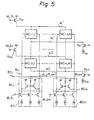
- Figure 5 is a schematic circuit diagram of a semiconductor memory device having the PNPN memory cell of Fig. 2.
- the semiconductor memory device of Fig. 5 comprises a group of pairs of first word lines W 1 + , ---, W + n and second word lines W - 1 ,-- -, W - n ; a group of pairs of bit lines BL 1 and BLZ,---, BL Zm ⁇ 1 and BL 2m ; and memory cells MC- 1,1 , ---, MC- n,m .
- the first word line W i + is connected to a word line drive transistor Q Di
- the second word line W i - is connected to a hold current source I HI through a discharge transistor Q Sl .
- the memory cell MC- i,j is connected between one pair of first word line W i + and second word line W,- and is also connected to one pair of bit lines BL 2j-1 and BL 2j Each pair of bit lines BL 2j ⁇ 1 and BL 2j is connected to a bit line clamp circuit BC j and to a bit line drive circuit BD j .
- a word line select signal WLS is applied to the base of the word line drive transistor Q DI
- a bit line select signal BLS j is applied to the bit line drive circuit BD j .
- a bit line clamp level signal BCL as applied to all the bit line clamp circuits BC 1 through BC m .
- Each memory cell MC- i,j has an equivalent circuit of Fig. 2.
- FIG. 6 A cross-sectional vertical view of the semiconductor memory device in accordance with the first embodiment of the present invention is illustrated in Fig. 6.
- the semiconductor memory device of Fig. 6 is formed on an N-type semiconductor substrate (N-SUB) 21.
- N-SUB N-type semiconductor substrate
- a high doping density P-type buried layer 22 is formed on the semiconductor substrate 21.
- a memory cell MC- 1,1 is formed on the buried layer 22 .
- the memory cell MC- 1 , 1 has a pair of PNPN elements, and each PNPN element is formed in a region surrounded by isolation regions ISO.
- an N-type region 23 is formed on the buried layer 22
- a P-type region 24 is formed on the N-type region 23, and two N-type regions 25 and 26 are formed separately on the P-type region 24.
- the load transistor Q 1 in the equivalent circuit of Fig. 2 is formed vertically by the P + -type buried layer 22, the N-type region 23, and the P-type region 24.
- the sense transistor Q 2 is formed vertically by the N-type region 23, the P-type region 24, and the N-type region 25.
- the hold transistor Q 3 is formed vertically by the N-type region 23, the P-type region 24, and the N-type region 26.
- the N-type region 23, the P-type region 24 and the N-type regions 25 and 26 are connected to metal wiring lines through contact windows (not shown) on the surface opposite to the N-type substrate 21.
- the N-type region 23 of one PNPN element is connected to the P-type region 24 of the other PNPN element by the metal wiring line.
- the N-type region 25 of one PNPN element is connected to the bit line BL,
- the N-type region 25 of the other PNPN element is connected to the bit line BL 2 .
- the N-type region 26 is connected to the second word line W - 1 .
- the buried layer 22 is formed commonly to the memory cells MC - 1,1 ,---, MC- 1,n connected to the first word line W 1 + and connected to the metal wiring line at the contact hole CH.
- the P +- type buried layer is used as the wiring layer for the first word line W 1 + .
- An NPN transistor Q o and a PNP transistor Q s may be formed as shown in Fig. 6.
- all the transistors Q 1 , Q 2 , and Q 3 of the PNPN element are formed vertically. This accordingly increases the switching speed and decreases the variation of the characteristic values.
- the buried layer is used as a wiring layer for a first word line W + . This accordingly decreases the metal wiring lines and eliminates two contact windows per memory cell. Thus, the area of memory cells can be decreased and the yield rate can be increased.
- a semiconductor memory device in accordance with a second embodiment of the present invention is illustrated in Fig. 7.
- the semiconductor memory device of Fig. 7 has PNPN type memory cells with the equivalent circuit of Fig. 2.
- the structure of the memory cell is different from that of the memory cell of Fig. 6.
- the semiconductor memory device of Fig. 7 is formed on a P-type semiconductor substrate 31.
- a high doping density N +- type buried layer 32 is formed on the P-type semiconductor substrate 31, and a P-type region 33 is formed on the N +- type buried layer 32.
- Two N-type regions 34 and 35 are formed separately on the P-type region 33.
- a P-type region 36 is formed on the N-type region 34.
- the load transistor Q 1 of the PNPN element is formed vertically by the P-type region 36, the N-type region 35, and the P-type region 33, and the hold transistor Q 3 is formed vertically by the N +- type buried layer 32, the P-type region 33, and the N-type region 35.
- the sense transistor Q 2 is formed laterally by the N-type region 34, the P-type region 33, and the N-type region 35.
- the P-type region 33, the N-type regions 34 and 35, and the P-type region 36 are connected to metal wiring lines through contact windows (not shown).
- the P-type region 33 of one PNPN element is connected to the N-type region 35 of the other PNPN element by the metal wiring line.
- the N-type region 34 is connected to the bit line BL 1 or BL 2 .
- the P-type region 36 is connected to the first word line W 1 + .
- the N +- type buried layer 31 is used as a wiring layer for the second word line W 1 - .
- the load transistor Q 1 and the hold transistor Q 3 are formed vertically. This accordingly increases the switching speed. Also, the N + buried layer 32 is used as a wiring layer for the second word line W-. This accordingly decreases the metal wiring lines and eliminates two contact windows per memory cell.
- FIG. 8 A semiconductor memory device in accordance with a third embodiment of the present invention is illustrated in Fig. 8.
- the semiconductor memory device of Fig. 8 has the same structure as the PNPN element of the Fig. 7 device, except that a high doping density P +- type region 37 is formed in the P-type region 33 between the N + -type buried layer 32 and the N-type region 34 in order to decrease the adverse influence due to a parasitic transistor Q v formed by the N +- type buried layer 32, the P-type region 33, and the P-type region 34.
- the sense transistor Q 2 can be replaced by the hold transistor Q 3 .
- the N +- type buried layer 32 may be used as a wiring layer for the bit line BL 1 or BL 2 .
- FIG. 9(A) and 9(B) A second type of PNPN memory cell is illustrated in Figs. 9(A) and 9(B).
- Figure 9(A) is an equivalent circuit diagram of this PNPN memory cell
- Fig. 9(B) is its model diagram.
- an NPN transistor Q 1 ' is used as a load transistor
- PNP transistors Q 2 ' and Q 3 ' are used as a sense transistor and a hold transistor.
- FIG. 10 A schematic circuit diagram of a semiconductor memory device having the memory cell of Figs. 9(A) and 9(B) is given in Fig. 10.
- the semiconductor memory device of Fig. 10 In the semiconductor memory device of Fig.
- the polarity of the signal lines and the conductivity type of the transistors are reversed from the semiconductor memory device of Fig. 5.
- the positive word lines W 1 + through W n + are connected to the hold current sources I H1 through I Hn
- the negative word lines W 1 - through W n - are connected to the word line drive PNP transistors Q D1 through Q Dn .
- the semiconductor memory device of Fig. 10 is constructed by reversing the conductivity type of the semiconductor memory device of Fig. 5.
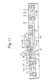
- FIG. 11 A semiconductor memory device in accordance with a fourth embodiment of the present invention is illustrated in Fig. 11.
- the semiconductor memory device of Fig. 11 has the same construction as the semiconductor memory device of Fig. 6, except that the conductivity type of each corresponding portion is reversed.
- each corresponding portion is denoted by the same reference numeral as in Fig. 6 but with an asterisk.
- the N +- type buried layer 22' is used as a wiring layer for the negative word line W 1 - , corresponding to the first word line W 1 + in Fig. 6.
- FIG. 12 A semiconductor memory device in accordance with a fifth embodiment of the present invention is illustrated in Fig. 12.
- the semiconductor memory device of Fig. 12 has the same construction as the semiconductor memory device of Fig. 11, except that the base-emitter junction of the sense transistor Q 2 is formed by a Schottky barrier diode (SBD).
- SBD Schottky barrier diode
- FIG. 13 A semiconductor memory device in accordance with a sixth embodiment of the present invention is illustrated in Fig. 13.
- the semiconductor memory device of Fig. 13 has the same construction as the semiconductor device of Fig. 7, except that the conductivity type of each corresponding portion is reversed.
- the corresponding portions are denoted by the same reference numerals as in Fig. 7 but with an asterisk.
Claims (12)
Applications Claiming Priority (4)
| Application Number | Priority Date | Filing Date | Title |
|---|---|---|---|
| JP57050092A JPS58168273A (ja) | 1982-03-30 | 1982-03-30 | 半導体記憶装置 |
| JP50092/82 | 1982-03-30 | ||
| JP51135/82 | 1982-03-31 | ||
| JP57051135A JPS6030108B2 (ja) | 1982-03-31 | 1982-03-31 | 半導体記憶装置 |
Publications (3)
| Publication Number | Publication Date |
|---|---|
| EP0090665A2 EP0090665A2 (fr) | 1983-10-05 |
| EP0090665A3 EP0090665A3 (en) | 1986-04-16 |
| EP0090665B1 true EP0090665B1 (fr) | 1989-05-31 |
Family
ID=26390529
Family Applications (1)
| Application Number | Title | Priority Date | Filing Date |
|---|---|---|---|
| EP83301824A Expired EP0090665B1 (fr) | 1982-03-30 | 1983-03-30 | Dispositif semi-conducteur à mémoire |
Country Status (3)
| Country | Link |
|---|---|
| US (1) | US4677455A (fr) |
| EP (1) | EP0090665B1 (fr) |
| DE (1) | DE3380004D1 (fr) |
Families Citing this family (35)
| Publication number | Priority date | Publication date | Assignee | Title |
|---|---|---|---|---|
| US5324982A (en) * | 1985-09-25 | 1994-06-28 | Hitachi, Ltd. | Semiconductor memory device having bipolar transistor and structure to avoid soft error |
| US6740958B2 (en) * | 1985-09-25 | 2004-05-25 | Renesas Technology Corp. | Semiconductor memory device |
| CH669068A5 (de) * | 1986-04-29 | 1989-02-15 | Landis & Gyr Ag | Integrierbares hallelement. |
| JP2675039B2 (ja) * | 1988-02-03 | 1997-11-12 | 株式会社日立製作所 | 半導体装置 |
| US4979011A (en) * | 1989-12-15 | 1990-12-18 | Harris Corporation | SCR structure for fast turn-on switching |
| EP0476308B1 (fr) * | 1990-09-20 | 1997-03-12 | Siemens Aktiengesellschaft | Transistor bipolaire pour fortes puissances en hyperfréquence |
| US5086242A (en) * | 1990-10-16 | 1992-02-04 | Harris Corporation | Fast turn-off of thyristor structure |
| US6229161B1 (en) * | 1998-06-05 | 2001-05-08 | Stanford University | Semiconductor capacitively-coupled NDR device and its applications in high-density high-speed memories and in power switches |
| US6690038B1 (en) | 1999-06-05 | 2004-02-10 | T-Ram, Inc. | Thyristor-based device over substrate surface |
| US6834308B1 (en) | 2000-02-17 | 2004-12-21 | Audible Magic Corporation | Method and apparatus for identifying media content presented on a media playing device |
| US8010988B2 (en) * | 2000-09-14 | 2011-08-30 | Cox Ingemar J | Using features extracted from an audio and/or video work to obtain information about the work |
| US8205237B2 (en) | 2000-09-14 | 2012-06-19 | Cox Ingemar J | Identifying works, using a sub-linear time search, such as an approximate nearest neighbor search, for initiating a work-based action, such as an action on the internet |
| US7562012B1 (en) | 2000-11-03 | 2009-07-14 | Audible Magic Corporation | Method and apparatus for creating a unique audio signature |
| US6727528B1 (en) | 2001-03-22 | 2004-04-27 | T-Ram, Inc. | Thyristor-based device including trench dielectric isolation for thyristor-body regions |
| US7456439B1 (en) | 2001-03-22 | 2008-11-25 | T-Ram Semiconductor, Inc. | Vertical thyristor-based memory with trench isolation and its method of fabrication |
| US6804162B1 (en) | 2001-04-05 | 2004-10-12 | T-Ram, Inc. | Read-modify-write memory using read-or-write banks |
| EP1490767B1 (fr) | 2001-04-05 | 2014-06-11 | Audible Magic Corporation | Detection de copyright et systeme et procede de protection |
| US7529659B2 (en) * | 2005-09-28 | 2009-05-05 | Audible Magic Corporation | Method and apparatus for identifying an unknown work |
| US6968337B2 (en) * | 2001-07-10 | 2005-11-22 | Audible Magic Corporation | Method and apparatus for identifying an unknown work |
| US8972481B2 (en) | 2001-07-20 | 2015-03-03 | Audible Magic, Inc. | Playlist generation method and apparatus |
| US7877438B2 (en) | 2001-07-20 | 2011-01-25 | Audible Magic Corporation | Method and apparatus for identifying new media content |
| US20030135623A1 (en) * | 2001-10-23 | 2003-07-17 | Audible Magic, Inc. | Method and apparatus for cache promotion |
| US6583452B1 (en) | 2001-12-17 | 2003-06-24 | T-Ram, Inc. | Thyristor-based device having extended capacitive coupling |
| US6832300B2 (en) | 2002-03-20 | 2004-12-14 | Hewlett-Packard Development Company, L.P. | Methods and apparatus for control of asynchronous cache |
| US6690039B1 (en) * | 2002-10-01 | 2004-02-10 | T-Ram, Inc. | Thyristor-based device that inhibits undesirable conductive channel formation |
| US6965129B1 (en) | 2002-11-06 | 2005-11-15 | T-Ram, Inc. | Thyristor-based device having dual control ports |
| US8332326B2 (en) * | 2003-02-01 | 2012-12-11 | Audible Magic Corporation | Method and apparatus to identify a work received by a processing system |
| KR100527559B1 (ko) * | 2004-02-05 | 2005-11-09 | 주식회사 하이닉스반도체 | 직렬 다이오드 셀을 이용한 불휘발성 메모리 장치 |
| KR100709463B1 (ko) * | 2004-02-16 | 2007-04-18 | 주식회사 하이닉스반도체 | 나노 튜브 셀을 이용한 메모리 장치 |
| KR100694426B1 (ko) * | 2004-02-16 | 2007-03-12 | 주식회사 하이닉스반도체 | 나노 튜브 셀 및 이를 이용한 메모리 장치 |
| KR100709462B1 (ko) * | 2004-02-16 | 2007-04-18 | 주식회사 하이닉스반도체 | 다층 나노 튜브 셀을 이용한 메모리 장치 |
| US8130746B2 (en) | 2004-07-28 | 2012-03-06 | Audible Magic Corporation | System for distributing decoy content in a peer to peer network |
| US8006314B2 (en) | 2007-07-27 | 2011-08-23 | Audible Magic Corporation | System for identifying content of digital data |
| US8199651B1 (en) | 2009-03-16 | 2012-06-12 | Audible Magic Corporation | Method and system for modifying communication flows at a port level |
| US9081778B2 (en) | 2012-09-25 | 2015-07-14 | Audible Magic Corporation | Using digital fingerprints to associate data with a work |
Family Cites Families (9)
| Publication number | Priority date | Publication date | Assignee | Title |
|---|---|---|---|---|
| DE1524892B1 (de) * | 1967-12-15 | 1970-09-03 | Ibm Deutschland | Halbleiterspeicherzelle mit kreuzgekoppelten Multie mittertransistoren |
| US3623029A (en) * | 1969-12-15 | 1971-11-23 | Ibm | Bistable multiemitter silicon-controlled rectifier storage cell |
| GB1434961A (en) * | 1973-11-08 | 1976-05-12 | Plessey Co Ltd | Integrated circuit arrangements |
| US3953866A (en) * | 1974-05-10 | 1976-04-27 | Signetics Corporation | Cross coupled semiconductor memory cell |
| NL7506844A (en) * | 1974-06-17 | 1975-08-29 | Xerox Corp | Integrated circuit for memory cells - employs monolithic construction of semiconductors with PNPN formation on epitaxial layers |
| DE2700587A1 (de) * | 1976-01-15 | 1977-07-21 | Itt Ind Gmbh Deutsche | Monolithisch integrierte i hoch 2 l-speicherzelle |
| FR2373163A1 (fr) * | 1976-12-03 | 1978-06-30 | Thomson Csf | Structure pour circuits logiques |
| NL186934C (nl) * | 1979-09-11 | 1991-04-02 | Philips Nv | Statische bipolaire geheugencel. |
| JPS5773956A (en) * | 1980-10-27 | 1982-05-08 | Hitachi Ltd | Glass coated semiconductor device |
-
1983
- 1983-03-30 EP EP83301824A patent/EP0090665B1/fr not_active Expired
- 1983-03-30 DE DE8383301824T patent/DE3380004D1/de not_active Expired
-
1986
- 1986-07-01 US US06/881,475 patent/US4677455A/en not_active Expired - Fee Related
Also Published As
| Publication number | Publication date |
|---|---|
| US4677455A (en) | 1987-06-30 |
| EP0090665A3 (en) | 1986-04-16 |
| DE3380004D1 (en) | 1989-07-06 |
| EP0090665A2 (fr) | 1983-10-05 |
Similar Documents
| Publication | Publication Date | Title |
|---|---|---|
| EP0090665B1 (fr) | Dispositif semi-conducteur à mémoire | |
| US4396999A (en) | Tunneling transistor memory cell | |
| EP0245515A1 (fr) | Dispositif a semi-conducteurs | |
| WO1999063598A1 (fr) | Dispositif de commutation de courant de semi-conducteur possedant un dispositif d'amelioration operationnel et procede correspond | |
| US4538244A (en) | Semiconductor memory device | |
| US4021786A (en) | Memory cell circuit and semiconductor structure therefore | |
| US4672416A (en) | Semiconductor device | |
| US5471419A (en) | Semiconductor device having a programmable memory cell | |
| EP0547673B1 (fr) | Dispositif semiconducteur muni d'au moins une cellule de mémoire | |
| US4399450A (en) | ROM With poly-Si to mono-Si diodes | |
| US4604728A (en) | Semiconductor memory device | |
| US4191899A (en) | Voltage variable integrated circuit capacitor and bootstrap driver circuit | |
| US4654688A (en) | Semiconductor device having a transistor with increased current amplification factor | |
| US5095355A (en) | Bipolar cross-coupled memory cells having improved immunity to soft errors | |
| EP0028157B1 (fr) | Circuit intégré semiconducteur à mémoire à logique d'injection intégrée | |
| JPS5842556B2 (ja) | 半導体記憶装置 | |
| US4231108A (en) | Semiconductor integrated circuit device | |
| EP0058845B1 (fr) | Cellule de mémoire à accès aléatoire | |
| EP0084000A2 (fr) | Dispositif CMOS | |
| US4170017A (en) | Highly integrated semiconductor structure providing a diode-resistor circuit configuration | |
| EP0071042B1 (fr) | Réseau de mémoire | |
| US5422841A (en) | Semiconductor memory device having reverse base current bipolar transistor-field effect transistor memory cell | |
| US4388636A (en) | Static memory cell and memory constructed from such cells | |
| EP0080351B1 (fr) | Transistors à émetteurs multiples dans des dispositifs de mémoires sémi-conductrices | |
| US4455625A (en) | Random access memory cell |
Legal Events
| Date | Code | Title | Description |
|---|---|---|---|
| PUAI | Public reference made under article 153(3) epc to a published international application that has entered the european phase |
Free format text: ORIGINAL CODE: 0009012 |
|
| AK | Designated contracting states |
Kind code of ref document: A2 Designated state(s): DE FR GB Designated state(s): DE FR GB |
|
| PUAL | Search report despatched |
Free format text: ORIGINAL CODE: 0009013 |
|
| AK | Designated contracting states |
Kind code of ref document: A3 Designated state(s): DE FR GB |
|
| 17P | Request for examination filed |
Effective date: 19860618 |
|
| 17Q | First examination report despatched |
Effective date: 19880629 |
|
| GRAA | (expected) grant |
Free format text: ORIGINAL CODE: 0009210 |
|
| AK | Designated contracting states |
Kind code of ref document: B1 Designated state(s): DE FR GB |
|
| REF | Corresponds to: |
Ref document number: 3380004 Country of ref document: DE Date of ref document: 19890706 |
|
| PGFP | Annual fee paid to national office [announced via postgrant information from national office to epo] |
Ref country code: FR Payment date: 19890707 Year of fee payment: 8 |
|
| ET | Fr: translation filed | ||
| PGFP | Annual fee paid to national office [announced via postgrant information from national office to epo] |
Ref country code: GB Payment date: 19900331 Year of fee payment: 8 |
|
| PLBE | No opposition filed within time limit |
Free format text: ORIGINAL CODE: 0009261 |
|
| STAA | Information on the status of an ep patent application or granted ep patent |
Free format text: STATUS: NO OPPOSITION FILED WITHIN TIME LIMIT |
|
| 26N | No opposition filed | ||
| PGFP | Annual fee paid to national office [announced via postgrant information from national office to epo] |
Ref country code: DE Payment date: 19900528 Year of fee payment: 8 |
|
| PG25 | Lapsed in a contracting state [announced via postgrant information from national office to epo] |
Ref country code: GB Effective date: 19910330 |
|
| GBPC | Gb: european patent ceased through non-payment of renewal fee | ||
| PG25 | Lapsed in a contracting state [announced via postgrant information from national office to epo] |
Ref country code: FR Effective date: 19911129 |
|
| PG25 | Lapsed in a contracting state [announced via postgrant information from national office to epo] |
Ref country code: DE Effective date: 19920101 |
|
| REG | Reference to a national code |
Ref country code: FR Ref legal event code: ST |