WO2009084590A1 - 高分子発光素子、製造方法及び高分子発光ディスプレイ装置 - Google Patents
高分子発光素子、製造方法及び高分子発光ディスプレイ装置 Download PDFInfo
- Publication number
- WO2009084590A1 WO2009084590A1 PCT/JP2008/073610 JP2008073610W WO2009084590A1 WO 2009084590 A1 WO2009084590 A1 WO 2009084590A1 JP 2008073610 W JP2008073610 W JP 2008073610W WO 2009084590 A1 WO2009084590 A1 WO 2009084590A1
- Authority
- WO
- WIPO (PCT)
- Prior art keywords
- layer
- electrode
- light emitting
- emitting device
- polymer
- Prior art date
Links
- 229920000642 polymer Polymers 0.000 title claims abstract description 110
- 238000000034 method Methods 0.000 title claims abstract description 85
- 238000004519 manufacturing process Methods 0.000 title claims abstract description 17
- 239000000463 material Substances 0.000 claims abstract description 119
- 150000001875 compounds Chemical class 0.000 claims abstract description 33
- 238000002834 transmittance Methods 0.000 claims abstract description 21
- 230000001603 reducing effect Effects 0.000 claims abstract description 17
- 229910052751 metal Inorganic materials 0.000 claims description 49
- 239000002184 metal Substances 0.000 claims description 49
- 239000000758 substrate Substances 0.000 claims description 47
- 239000000203 mixture Substances 0.000 claims description 46
- 239000011777 magnesium Substances 0.000 claims description 30
- 239000011575 calcium Substances 0.000 claims description 29
- PUZPDOWCWNUUKD-UHFFFAOYSA-M sodium fluoride Chemical compound [F-].[Na+] PUZPDOWCWNUUKD-UHFFFAOYSA-M 0.000 claims description 26
- 229910044991 metal oxide Inorganic materials 0.000 claims description 19
- 150000004706 metal oxides Chemical class 0.000 claims description 19
- 150000002739 metals Chemical class 0.000 claims description 17
- 238000001771 vacuum deposition Methods 0.000 claims description 17
- 229910001512 metal fluoride Inorganic materials 0.000 claims description 14
- 239000011775 sodium fluoride Substances 0.000 claims description 13
- 235000013024 sodium fluoride Nutrition 0.000 claims description 13
- 229910052782 aluminium Inorganic materials 0.000 claims description 12
- 229910052709 silver Inorganic materials 0.000 claims description 12
- 229910052791 calcium Inorganic materials 0.000 claims description 11
- OYPRJOBELJOOCE-UHFFFAOYSA-N Calcium Chemical compound [Ca] OYPRJOBELJOOCE-UHFFFAOYSA-N 0.000 claims description 10
- FYYHWMGAXLPEAU-UHFFFAOYSA-N Magnesium Chemical compound [Mg] FYYHWMGAXLPEAU-UHFFFAOYSA-N 0.000 claims description 10
- 229910045601 alloy Inorganic materials 0.000 claims description 10
- 239000000956 alloy Substances 0.000 claims description 10
- 239000003638 chemical reducing agent Substances 0.000 claims description 10
- 229910052749 magnesium Inorganic materials 0.000 claims description 10
- 239000010949 copper Substances 0.000 claims description 9
- PXHVJJICTQNCMI-UHFFFAOYSA-N Nickel Chemical compound [Ni] PXHVJJICTQNCMI-UHFFFAOYSA-N 0.000 claims description 8
- XAGFODPZIPBFFR-UHFFFAOYSA-N aluminium Chemical compound [Al] XAGFODPZIPBFFR-UHFFFAOYSA-N 0.000 claims description 8
- 239000004332 silver Substances 0.000 claims description 8
- BQCADISMDOOEFD-UHFFFAOYSA-N Silver Chemical compound [Ag] BQCADISMDOOEFD-UHFFFAOYSA-N 0.000 claims description 6
- 239000011734 sodium Substances 0.000 claims description 6
- QVQLCTNNEUAWMS-UHFFFAOYSA-N barium oxide Chemical compound [Ba]=O QVQLCTNNEUAWMS-UHFFFAOYSA-N 0.000 claims description 5
- 229910052737 gold Inorganic materials 0.000 claims description 5
- 239000010931 gold Substances 0.000 claims description 5
- DGAQECJNVWCQMB-PUAWFVPOSA-M Ilexoside XXIX Chemical compound C[C@@H]1CC[C@@]2(CC[C@@]3(C(=CC[C@H]4[C@]3(CC[C@@H]5[C@@]4(CC[C@@H](C5(C)C)OS(=O)(=O)[O-])C)C)[C@@H]2[C@]1(C)O)C)C(=O)O[C@H]6[C@@H]([C@H]([C@@H]([C@H](O6)CO)O)O)O.[Na+] DGAQECJNVWCQMB-PUAWFVPOSA-M 0.000 claims description 4
- 229910052783 alkali metal Inorganic materials 0.000 claims description 4
- 150000001340 alkali metals Chemical class 0.000 claims description 4
- 229910052784 alkaline earth metal Inorganic materials 0.000 claims description 4
- 150000001342 alkaline earth metals Chemical class 0.000 claims description 4
- 229910052788 barium Inorganic materials 0.000 claims description 4
- DSAJWYNOEDNPEQ-UHFFFAOYSA-N barium atom Chemical compound [Ba] DSAJWYNOEDNPEQ-UHFFFAOYSA-N 0.000 claims description 4
- 229910052802 copper Inorganic materials 0.000 claims description 4
- PCHJSUWPFVWCPO-UHFFFAOYSA-N gold Chemical compound [Au] PCHJSUWPFVWCPO-UHFFFAOYSA-N 0.000 claims description 4
- 229910052759 nickel Inorganic materials 0.000 claims description 4
- 230000008569 process Effects 0.000 claims description 4
- 229910052701 rubidium Inorganic materials 0.000 claims description 4
- IGLNJRXAVVLDKE-UHFFFAOYSA-N rubidium atom Chemical compound [Rb] IGLNJRXAVVLDKE-UHFFFAOYSA-N 0.000 claims description 4
- AHLATJUETSFVIM-UHFFFAOYSA-M rubidium fluoride Chemical compound [F-].[Rb+] AHLATJUETSFVIM-UHFFFAOYSA-M 0.000 claims description 4
- 229910052708 sodium Inorganic materials 0.000 claims description 4
- 239000011135 tin Substances 0.000 claims description 4
- RYGMFSIKBFXOCR-UHFFFAOYSA-N Copper Chemical compound [Cu] RYGMFSIKBFXOCR-UHFFFAOYSA-N 0.000 claims description 3
- ATJFFYVFTNAWJD-UHFFFAOYSA-N Tin Chemical compound [Sn] ATJFFYVFTNAWJD-UHFFFAOYSA-N 0.000 claims description 3
- 229910001515 alkali metal fluoride Inorganic materials 0.000 claims description 3
- 229910000272 alkali metal oxide Inorganic materials 0.000 claims description 3
- 229910001618 alkaline earth metal fluoride Inorganic materials 0.000 claims description 3
- 229910000287 alkaline earth metal oxide Inorganic materials 0.000 claims description 3
- 229910052738 indium Inorganic materials 0.000 claims description 3
- APFVFJFRJDLVQX-UHFFFAOYSA-N indium atom Chemical compound [In] APFVFJFRJDLVQX-UHFFFAOYSA-N 0.000 claims description 3
- 239000011133 lead Substances 0.000 claims description 3
- 229910052718 tin Inorganic materials 0.000 claims description 3
- OYLGJCQECKOTOL-UHFFFAOYSA-L barium fluoride Chemical compound [F-].[F-].[Ba+2] OYLGJCQECKOTOL-UHFFFAOYSA-L 0.000 claims description 2
- 229910001632 barium fluoride Inorganic materials 0.000 claims description 2
- 229910001952 rubidium oxide Inorganic materials 0.000 claims description 2
- CWBWCLMMHLCMAM-UHFFFAOYSA-M rubidium(1+);hydroxide Chemical compound [OH-].[Rb+].[Rb+] CWBWCLMMHLCMAM-UHFFFAOYSA-M 0.000 claims description 2
- KKCBUQHMOMHUOY-UHFFFAOYSA-N sodium oxide Chemical compound [O-2].[Na+].[Na+] KKCBUQHMOMHUOY-UHFFFAOYSA-N 0.000 claims description 2
- 229910001948 sodium oxide Inorganic materials 0.000 claims description 2
- 239000010410 layer Substances 0.000 description 597
- 238000002347 injection Methods 0.000 description 84
- 239000007924 injection Substances 0.000 description 84
- 230000005525 hole transport Effects 0.000 description 53
- 239000010408 film Substances 0.000 description 37
- 239000011229 interlayer Substances 0.000 description 28
- 238000000576 coating method Methods 0.000 description 26
- -1 amino-substituted chalcones Chemical class 0.000 description 24
- 230000000903 blocking effect Effects 0.000 description 22
- 239000000243 solution Substances 0.000 description 17
- 230000015572 biosynthetic process Effects 0.000 description 15
- 230000000052 comparative effect Effects 0.000 description 14
- 239000011248 coating agent Substances 0.000 description 12
- 238000007639 printing Methods 0.000 description 11
- 239000002904 solvent Substances 0.000 description 11
- 229910019015 Mg-Ag Inorganic materials 0.000 description 10
- 125000003118 aryl group Chemical group 0.000 description 10
- RAXXELZNTBOGNW-UHFFFAOYSA-N imidazole Natural products C1=CNC=N1 RAXXELZNTBOGNW-UHFFFAOYSA-N 0.000 description 9
- 239000002861 polymer material Substances 0.000 description 9
- 238000004132 cross linking Methods 0.000 description 8
- 125000001424 substituent group Chemical group 0.000 description 8
- 229910016036 BaF 2 Inorganic materials 0.000 description 7
- UJOBWOGCFQCDNV-UHFFFAOYSA-N 9H-carbazole Chemical compound C1=CC=C2C3=CC=CC=C3NC2=C1 UJOBWOGCFQCDNV-UHFFFAOYSA-N 0.000 description 6
- KRHYYFGTRYWZRS-UHFFFAOYSA-M Fluoride anion Chemical compound [F-] KRHYYFGTRYWZRS-UHFFFAOYSA-M 0.000 description 6
- 150000004982 aromatic amines Chemical class 0.000 description 6
- 229920001577 copolymer Polymers 0.000 description 6
- 239000000975 dye Substances 0.000 description 6
- 229920003227 poly(N-vinyl carbazole) Polymers 0.000 description 6
- 238000004528 spin coating Methods 0.000 description 6
- 229910016569 AlF 3 Inorganic materials 0.000 description 5
- CTQNGGLPUBDAKN-UHFFFAOYSA-N O-Xylene Chemical compound CC1=CC=CC=C1C CTQNGGLPUBDAKN-UHFFFAOYSA-N 0.000 description 5
- 238000010549 co-Evaporation Methods 0.000 description 5
- 150000004696 coordination complex Chemical class 0.000 description 5
- YLQWCDOCJODRMT-UHFFFAOYSA-N fluoren-9-one Chemical compound C1=CC=C2C(=O)C3=CC=CC=C3C2=C1 YLQWCDOCJODRMT-UHFFFAOYSA-N 0.000 description 5
- 125000000623 heterocyclic group Chemical group 0.000 description 5
- 239000011159 matrix material Substances 0.000 description 5
- 238000007789 sealing Methods 0.000 description 5
- 239000008096 xylene Substances 0.000 description 5
- 229910018072 Al 2 O 3 Inorganic materials 0.000 description 4
- PAYRUJLWNCNPSJ-UHFFFAOYSA-N Aniline Chemical compound NC1=CC=CC=C1 PAYRUJLWNCNPSJ-UHFFFAOYSA-N 0.000 description 4
- 229910004261 CaF 2 Inorganic materials 0.000 description 4
- UFWIBTONFRDIAS-UHFFFAOYSA-N Naphthalene Chemical compound C1=CC=CC2=CC=CC=C21 UFWIBTONFRDIAS-UHFFFAOYSA-N 0.000 description 4
- ZCQWOFVYLHDMMC-UHFFFAOYSA-N Oxazole Chemical compound C1=COC=N1 ZCQWOFVYLHDMMC-UHFFFAOYSA-N 0.000 description 4
- 229910020836 Sn-Ag Inorganic materials 0.000 description 4
- 229910020988 Sn—Ag Inorganic materials 0.000 description 4
- PJANXHGTPQOBST-VAWYXSNFSA-N Stilbene Natural products C=1C=CC=CC=1/C=C/C1=CC=CC=C1 PJANXHGTPQOBST-VAWYXSNFSA-N 0.000 description 4
- YTPLMLYBLZKORZ-UHFFFAOYSA-N Thiophene Chemical compound C=1C=CSC=1 YTPLMLYBLZKORZ-UHFFFAOYSA-N 0.000 description 4
- 238000007611 bar coating method Methods 0.000 description 4
- 238000007756 gravure coating Methods 0.000 description 4
- 238000007646 gravure printing Methods 0.000 description 4
- 238000007641 inkjet printing Methods 0.000 description 4
- 238000007645 offset printing Methods 0.000 description 4
- WCPAKWJPBJAGKN-UHFFFAOYSA-N oxadiazole Chemical compound C1=CON=N1 WCPAKWJPBJAGKN-UHFFFAOYSA-N 0.000 description 4
- 229960003540 oxyquinoline Drugs 0.000 description 4
- 125000002080 perylenyl group Chemical group C1(=CC=C2C=CC=C3C4=CC=CC5=CC=CC(C1=C23)=C45)* 0.000 description 4
- CSHWQDPOILHKBI-UHFFFAOYSA-N peryrene Natural products C1=CC(C2=CC=CC=3C2=C2C=CC=3)=C3C2=CC=CC3=C1 CSHWQDPOILHKBI-UHFFFAOYSA-N 0.000 description 4
- 229920002098 polyfluorene Polymers 0.000 description 4
- 229920005596 polymer binder Polymers 0.000 description 4
- 239000002491 polymer binding agent Substances 0.000 description 4
- 229920000123 polythiophene Polymers 0.000 description 4
- DNXIASIHZYFFRO-UHFFFAOYSA-N pyrazoline Chemical compound C1CN=NC1 DNXIASIHZYFFRO-UHFFFAOYSA-N 0.000 description 4
- MCJGNVYPOGVAJF-UHFFFAOYSA-N quinolin-8-ol Chemical compound C1=CN=C2C(O)=CC=CC2=C1 MCJGNVYPOGVAJF-UHFFFAOYSA-N 0.000 description 4
- 238000007650 screen-printing Methods 0.000 description 4
- 150000004756 silanes Chemical class 0.000 description 4
- 239000002356 single layer Substances 0.000 description 4
- PJANXHGTPQOBST-UHFFFAOYSA-N stilbene Chemical compound C=1C=CC=CC=1C=CC1=CC=CC=C1 PJANXHGTPQOBST-UHFFFAOYSA-N 0.000 description 4
- 235000021286 stilbenes Nutrition 0.000 description 4
- 150000003852 triazoles Chemical class 0.000 description 4
- 238000007740 vapor deposition Methods 0.000 description 4
- UWRZIZXBOLBCON-VOTSOKGWSA-N (e)-2-phenylethenamine Chemical class N\C=C\C1=CC=CC=C1 UWRZIZXBOLBCON-VOTSOKGWSA-N 0.000 description 3
- GEYOCULIXLDCMW-UHFFFAOYSA-N 1,2-phenylenediamine Chemical compound NC1=CC=CC=C1N GEYOCULIXLDCMW-UHFFFAOYSA-N 0.000 description 3
- AZQWKYJCGOJGHM-UHFFFAOYSA-N 1,4-benzoquinone Chemical compound O=C1C=CC(=O)C=C1 AZQWKYJCGOJGHM-UHFFFAOYSA-N 0.000 description 3
- VERMWGQSKPXSPZ-BUHFOSPRSA-N 1-[(e)-2-phenylethenyl]anthracene Chemical compound C=1C=CC2=CC3=CC=CC=C3C=C2C=1\C=C\C1=CC=CC=C1 VERMWGQSKPXSPZ-BUHFOSPRSA-N 0.000 description 3
- ZWEHNKRNPOVVGH-UHFFFAOYSA-N 2-Butanone Chemical compound CCC(C)=O ZWEHNKRNPOVVGH-UHFFFAOYSA-N 0.000 description 3
- 239000005725 8-Hydroxyquinoline Substances 0.000 description 3
- DQFBYFPFKXHELB-UHFFFAOYSA-N Chalcone Natural products C=1C=CC=CC=1C(=O)C=CC1=CC=CC=C1 DQFBYFPFKXHELB-UHFFFAOYSA-N 0.000 description 3
- YMWUJEATGCHHMB-UHFFFAOYSA-N Dichloromethane Chemical compound ClCCl YMWUJEATGCHHMB-UHFFFAOYSA-N 0.000 description 3
- XEKOWRVHYACXOJ-UHFFFAOYSA-N Ethyl acetate Chemical compound CCOC(C)=O XEKOWRVHYACXOJ-UHFFFAOYSA-N 0.000 description 3
- WHXSMMKQMYFTQS-UHFFFAOYSA-N Lithium Chemical compound [Li] WHXSMMKQMYFTQS-UHFFFAOYSA-N 0.000 description 3
- 229920000265 Polyparaphenylene Polymers 0.000 description 3
- 229920000292 Polyquinoline Polymers 0.000 description 3
- 239000004793 Polystyrene Substances 0.000 description 3
- YXFVVABEGXRONW-UHFFFAOYSA-N Toluene Chemical compound CC1=CC=CC=C1 YXFVVABEGXRONW-UHFFFAOYSA-N 0.000 description 3
- 150000004056 anthraquinones Chemical class 0.000 description 3
- 125000000732 arylene group Chemical group 0.000 description 3
- 239000000872 buffer Substances 0.000 description 3
- 235000005513 chalcones Nutrition 0.000 description 3
- 238000006243 chemical reaction Methods 0.000 description 3
- 229920000547 conjugated polymer Polymers 0.000 description 3
- 238000010494 dissociation reaction Methods 0.000 description 3
- 230000005593 dissociations Effects 0.000 description 3
- 239000003822 epoxy resin Substances 0.000 description 3
- 239000011521 glass Substances 0.000 description 3
- 150000007857 hydrazones Chemical class 0.000 description 3
- 229910052763 palladium Inorganic materials 0.000 description 3
- 229920003229 poly(methyl methacrylate) Polymers 0.000 description 3
- 229920000548 poly(silane) polymer Chemical class 0.000 description 3
- 229920000515 polycarbonate Polymers 0.000 description 3
- 239000004417 polycarbonate Substances 0.000 description 3
- 229920000647 polyepoxide Polymers 0.000 description 3
- 239000004926 polymethyl methacrylate Substances 0.000 description 3
- 229920002223 polystyrene Polymers 0.000 description 3
- 229920000915 polyvinyl chloride Polymers 0.000 description 3
- 239000004800 polyvinyl chloride Substances 0.000 description 3
- JEXVQSWXXUJEMA-UHFFFAOYSA-N pyrazol-3-one Chemical compound O=C1C=CN=N1 JEXVQSWXXUJEMA-UHFFFAOYSA-N 0.000 description 3
- 238000012546 transfer Methods 0.000 description 3
- KLCLIOISYBHYDZ-UHFFFAOYSA-N 1,4,4-triphenylbuta-1,3-dienylbenzene Chemical compound C=1C=CC=CC=1C(C=1C=CC=CC=1)=CC=C(C=1C=CC=CC=1)C1=CC=CC=C1 KLCLIOISYBHYDZ-UHFFFAOYSA-N 0.000 description 2
- FRASJONUBLZVQX-UHFFFAOYSA-N 1,4-naphthoquinone Chemical compound C1=CC=C2C(=O)C=CC(=O)C2=C1 FRASJONUBLZVQX-UHFFFAOYSA-N 0.000 description 2
- DDTHMESPCBONDT-UHFFFAOYSA-N 4-(4-oxocyclohexa-2,5-dien-1-ylidene)cyclohexa-2,5-dien-1-one Chemical compound C1=CC(=O)C=CC1=C1C=CC(=O)C=C1 DDTHMESPCBONDT-UHFFFAOYSA-N 0.000 description 2
- CSCPPACGZOOCGX-UHFFFAOYSA-N Acetone Chemical compound CC(C)=O CSCPPACGZOOCGX-UHFFFAOYSA-N 0.000 description 2
- NIXOWILDQLNWCW-UHFFFAOYSA-M Acrylate Chemical compound [O-]C(=O)C=C NIXOWILDQLNWCW-UHFFFAOYSA-M 0.000 description 2
- HEDRZPFGACZZDS-UHFFFAOYSA-N Chloroform Chemical compound ClC(Cl)Cl HEDRZPFGACZZDS-UHFFFAOYSA-N 0.000 description 2
- 229920002319 Poly(methyl acrylate) Polymers 0.000 description 2
- WYURNTSHIVDZCO-UHFFFAOYSA-N Tetrahydrofuran Chemical compound C1CCOC1 WYURNTSHIVDZCO-UHFFFAOYSA-N 0.000 description 2
- XLOMVQKBTHCTTD-UHFFFAOYSA-N Zinc monoxide Chemical compound [Zn]=O XLOMVQKBTHCTTD-UHFFFAOYSA-N 0.000 description 2
- 125000003277 amino group Chemical group 0.000 description 2
- MWPLVEDNUUSJAV-UHFFFAOYSA-N anthracene Chemical compound C1=CC=CC2=CC3=CC=CC=C3C=C21 MWPLVEDNUUSJAV-UHFFFAOYSA-N 0.000 description 2
- PYKYMHQGRFAEBM-UHFFFAOYSA-N anthraquinone Natural products CCC(=O)c1c(O)c2C(=O)C3C(C=CC=C3O)C(=O)c2cc1CC(=O)OC PYKYMHQGRFAEBM-UHFFFAOYSA-N 0.000 description 2
- IOJUPLGTWVMSFF-UHFFFAOYSA-N benzothiazole Chemical compound C1=CC=C2SC=NC2=C1 IOJUPLGTWVMSFF-UHFFFAOYSA-N 0.000 description 2
- 238000005266 casting Methods 0.000 description 2
- 229920001940 conductive polymer Polymers 0.000 description 2
- 239000004020 conductor Substances 0.000 description 2
- ZYGHJZDHTFUPRJ-UHFFFAOYSA-N coumarin Chemical compound C1=CC=C2OC(=O)C=CC2=C1 ZYGHJZDHTFUPRJ-UHFFFAOYSA-N 0.000 description 2
- 239000003431 cross linking reagent Substances 0.000 description 2
- ZSWFCLXCOIISFI-UHFFFAOYSA-N cyclopentadiene Chemical compound C1C=CC=C1 ZSWFCLXCOIISFI-UHFFFAOYSA-N 0.000 description 2
- 238000013461 design Methods 0.000 description 2
- 238000003618 dip coating Methods 0.000 description 2
- 230000005684 electric field Effects 0.000 description 2
- 238000005401 electroluminescence Methods 0.000 description 2
- 125000004185 ester group Chemical group 0.000 description 2
- 238000011156 evaluation Methods 0.000 description 2
- 238000010438 heat treatment Methods 0.000 description 2
- 238000010030 laminating Methods 0.000 description 2
- 239000011259 mixed solution Substances 0.000 description 2
- 229910052750 molybdenum Inorganic materials 0.000 description 2
- 229910000476 molybdenum oxide Inorganic materials 0.000 description 2
- 239000012299 nitrogen atmosphere Substances 0.000 description 2
- 150000002894 organic compounds Chemical class 0.000 description 2
- PQQKPALAQIIWST-UHFFFAOYSA-N oxomolybdenum Chemical compound [Mo]=O PQQKPALAQIIWST-UHFFFAOYSA-N 0.000 description 2
- 125000000843 phenylene group Chemical group C1(=C(C=CC=C1)*)* 0.000 description 2
- 239000002798 polar solvent Substances 0.000 description 2
- 229920000058 polyacrylate Polymers 0.000 description 2
- 229920000767 polyaniline Polymers 0.000 description 2
- 229920000412 polyarylene Polymers 0.000 description 2
- 229920000128 polypyrrole Polymers 0.000 description 2
- 229920001296 polysiloxane Polymers 0.000 description 2
- 230000007261 regionalization Effects 0.000 description 2
- 239000005394 sealing glass Substances 0.000 description 2
- 150000003378 silver Chemical class 0.000 description 2
- 238000009751 slip forming Methods 0.000 description 2
- 150000003384 small molecules Chemical class 0.000 description 2
- 238000005507 spraying Methods 0.000 description 2
- 238000004544 sputter deposition Methods 0.000 description 2
- 239000000126 substance Substances 0.000 description 2
- 239000010409 thin film Substances 0.000 description 2
- 229930192474 thiophene Natural products 0.000 description 2
- 125000000391 vinyl group Chemical group [H]C([*])=C([H])[H] 0.000 description 2
- QGKMIGUHVLGJBR-UHFFFAOYSA-M (4z)-1-(3-methylbutyl)-4-[[1-(3-methylbutyl)quinolin-1-ium-4-yl]methylidene]quinoline;iodide Chemical compound [I-].C12=CC=CC=C2N(CCC(C)C)C=CC1=CC1=CC=[N+](CCC(C)C)C2=CC=CC=C12 QGKMIGUHVLGJBR-UHFFFAOYSA-M 0.000 description 1
- SCYULBFZEHDVBN-UHFFFAOYSA-N 1,1-Dichloroethane Chemical compound CC(Cl)Cl SCYULBFZEHDVBN-UHFFFAOYSA-N 0.000 description 1
- FNQJDLTXOVEEFB-UHFFFAOYSA-N 1,2,3-benzothiadiazole Chemical compound C1=CC=C2SN=NC2=C1 FNQJDLTXOVEEFB-UHFFFAOYSA-N 0.000 description 1
- OURODNXVJUWPMZ-UHFFFAOYSA-N 1,2-diphenylanthracene Chemical compound C1=CC=CC=C1C1=CC=C(C=C2C(C=CC=C2)=C2)C2=C1C1=CC=CC=C1 OURODNXVJUWPMZ-UHFFFAOYSA-N 0.000 description 1
- SULWTXOWAFVWOY-PHEQNACWSA-N 2,3-bis[(E)-2-phenylethenyl]pyrazine Chemical compound C=1C=CC=CC=1/C=C/C1=NC=CN=C1\C=C\C1=CC=CC=C1 SULWTXOWAFVWOY-PHEQNACWSA-N 0.000 description 1
- VFBJMPNFKOMEEW-UHFFFAOYSA-N 2,3-diphenylbut-2-enedinitrile Chemical group C=1C=CC=CC=1C(C#N)=C(C#N)C1=CC=CC=C1 VFBJMPNFKOMEEW-UHFFFAOYSA-N 0.000 description 1
- IXHWGNYCZPISET-UHFFFAOYSA-N 2-[4-(dicyanomethylidene)-2,3,5,6-tetrafluorocyclohexa-2,5-dien-1-ylidene]propanedinitrile Chemical compound FC1=C(F)C(=C(C#N)C#N)C(F)=C(F)C1=C(C#N)C#N IXHWGNYCZPISET-UHFFFAOYSA-N 0.000 description 1
- SVONRAPFKPVNKG-UHFFFAOYSA-N 2-ethoxyethyl acetate Chemical compound CCOCCOC(C)=O SVONRAPFKPVNKG-UHFFFAOYSA-N 0.000 description 1
- GOLORTLGFDVFDW-UHFFFAOYSA-N 3-(1h-benzimidazol-2-yl)-7-(diethylamino)chromen-2-one Chemical compound C1=CC=C2NC(C3=CC4=CC=C(C=C4OC3=O)N(CC)CC)=NC2=C1 GOLORTLGFDVFDW-UHFFFAOYSA-N 0.000 description 1
- ZYASLTYCYTYKFC-UHFFFAOYSA-N 9-methylidenefluorene Chemical compound C1=CC=C2C(=C)C3=CC=CC=C3C2=C1 ZYASLTYCYTYKFC-UHFFFAOYSA-N 0.000 description 1
- GJCOSYZMQJWQCA-UHFFFAOYSA-N 9H-xanthene Chemical compound C1=CC=C2CC3=CC=CC=C3OC2=C1 GJCOSYZMQJWQCA-UHFFFAOYSA-N 0.000 description 1
- 239000005964 Acibenzolar-S-methyl Substances 0.000 description 1
- HRPVXLWXLXDGHG-UHFFFAOYSA-N Acrylamide Chemical compound NC(=O)C=C HRPVXLWXLXDGHG-UHFFFAOYSA-N 0.000 description 1
- 229910001316 Ag alloy Inorganic materials 0.000 description 1
- 229910000838 Al alloy Inorganic materials 0.000 description 1
- DKPFZGUDAPQIHT-UHFFFAOYSA-N Butyl acetate Natural products CCCCOC(C)=O DKPFZGUDAPQIHT-UHFFFAOYSA-N 0.000 description 1
- DQKRVYDATAXCHR-UHFFFAOYSA-N C(=C)N[SiH2]O Chemical compound C(=C)N[SiH2]O DQKRVYDATAXCHR-UHFFFAOYSA-N 0.000 description 1
- ZMISUKYBTKEKGE-UHFFFAOYSA-N CCCC1=CCC(C(C)CC)C=C1 Chemical compound CCCC1=CCC(C(C)CC)C=C1 ZMISUKYBTKEKGE-UHFFFAOYSA-N 0.000 description 1
- ZAMOUSCENKQFHK-UHFFFAOYSA-N Chlorine atom Chemical compound [Cl] ZAMOUSCENKQFHK-UHFFFAOYSA-N 0.000 description 1
- VYZAMTAEIAYCRO-UHFFFAOYSA-N Chromium Chemical compound [Cr] VYZAMTAEIAYCRO-UHFFFAOYSA-N 0.000 description 1
- 241000284156 Clerodendrum quadriloculare Species 0.000 description 1
- ZZSNKZQZMQGXPY-UHFFFAOYSA-N Ethyl cellulose Chemical compound CCOCC1OC(OC)C(OCC)C(OCC)C1OC1C(O)C(O)C(OC)C(CO)O1 ZZSNKZQZMQGXPY-UHFFFAOYSA-N 0.000 description 1
- 239000001856 Ethyl cellulose Substances 0.000 description 1
- 239000013032 Hydrocarbon resin Substances 0.000 description 1
- 229920000877 Melamine resin Polymers 0.000 description 1
- 239000004640 Melamine resin Substances 0.000 description 1
- CERQOIWHTDAKMF-UHFFFAOYSA-M Methacrylate Chemical compound CC(=C)C([O-])=O CERQOIWHTDAKMF-UHFFFAOYSA-M 0.000 description 1
- GXCLVBGFBYZDAG-UHFFFAOYSA-N N-[2-(1H-indol-3-yl)ethyl]-N-methylprop-2-en-1-amine Chemical compound CN(CCC1=CNC2=C1C=CC=C2)CC=C GXCLVBGFBYZDAG-UHFFFAOYSA-N 0.000 description 1
- 229930192627 Naphthoquinone Natural products 0.000 description 1
- 229920001609 Poly(3,4-ethylenedioxythiophene) Polymers 0.000 description 1
- 239000004952 Polyamide Substances 0.000 description 1
- 239000005062 Polybutadiene Substances 0.000 description 1
- 239000004721 Polyphenylene oxide Substances 0.000 description 1
- ZLMJMSJWJFRBEC-UHFFFAOYSA-N Potassium Chemical compound [K] ZLMJMSJWJFRBEC-UHFFFAOYSA-N 0.000 description 1
- NRCMAYZCPIVABH-UHFFFAOYSA-N Quinacridone Chemical compound N1C2=CC=CC=C2C(=O)C2=C1C=C1C(=O)C3=CC=CC=C3NC1=C2 NRCMAYZCPIVABH-UHFFFAOYSA-N 0.000 description 1
- XUIMIQQOPSSXEZ-UHFFFAOYSA-N Silicon Chemical compound [Si] XUIMIQQOPSSXEZ-UHFFFAOYSA-N 0.000 description 1
- XTXRWKRVRITETP-UHFFFAOYSA-N Vinyl acetate Chemical compound CC(=O)OC=C XTXRWKRVRITETP-UHFFFAOYSA-N 0.000 description 1
- QYKIQEUNHZKYBP-UHFFFAOYSA-N Vinyl ether Chemical compound C=COC=C QYKIQEUNHZKYBP-UHFFFAOYSA-N 0.000 description 1
- XHCLAFWTIXFWPH-UHFFFAOYSA-N [O-2].[O-2].[O-2].[O-2].[O-2].[V+5].[V+5] Chemical compound [O-2].[O-2].[O-2].[O-2].[O-2].[V+5].[V+5] XHCLAFWTIXFWPH-UHFFFAOYSA-N 0.000 description 1
- 239000002253 acid Substances 0.000 description 1
- 229920000122 acrylonitrile butadiene styrene Polymers 0.000 description 1
- 125000003647 acryloyl group Chemical group O=C([*])C([H])=C([H])[H] 0.000 description 1
- 125000002252 acyl group Chemical group 0.000 description 1
- 125000004423 acyloxy group Chemical group 0.000 description 1
- 125000003342 alkenyl group Chemical group 0.000 description 1
- 125000003545 alkoxy group Chemical group 0.000 description 1
- 125000004453 alkoxycarbonyl group Chemical group 0.000 description 1
- 229920000180 alkyd Polymers 0.000 description 1
- 125000000217 alkyl group Chemical group 0.000 description 1
- 125000004414 alkyl thio group Chemical group 0.000 description 1
- 125000000304 alkynyl group Chemical group 0.000 description 1
- 125000003368 amide group Chemical group 0.000 description 1
- 150000001412 amines Chemical class 0.000 description 1
- 229910003481 amorphous carbon Inorganic materials 0.000 description 1
- RJGDLRCDCYRQOQ-UHFFFAOYSA-N anthrone Chemical compound C1=CC=C2C(=O)C3=CC=CC=C3CC2=C1 RJGDLRCDCYRQOQ-UHFFFAOYSA-N 0.000 description 1
- 150000004945 aromatic hydrocarbons Chemical class 0.000 description 1
- 125000005018 aryl alkenyl group Chemical group 0.000 description 1
- 125000005098 aryl alkoxy carbonyl group Chemical group 0.000 description 1
- 125000003710 aryl alkyl group Chemical group 0.000 description 1
- 125000004659 aryl alkyl thio group Chemical group 0.000 description 1
- 125000002102 aryl alkyloxo group Chemical group 0.000 description 1
- 125000005015 aryl alkynyl group Chemical group 0.000 description 1
- 125000005161 aryl oxy carbonyl group Chemical group 0.000 description 1
- 125000005110 aryl thio group Chemical group 0.000 description 1
- 125000004104 aryloxy group Chemical group 0.000 description 1
- QVGXLLKOCUKJST-UHFFFAOYSA-N atomic oxygen Chemical compound [O] QVGXLLKOCUKJST-UHFFFAOYSA-N 0.000 description 1
- 150000001558 benzoic acid derivatives Chemical class 0.000 description 1
- 229910052790 beryllium Inorganic materials 0.000 description 1
- ATBAMAFKBVZNFJ-UHFFFAOYSA-N beryllium atom Chemical compound [Be] ATBAMAFKBVZNFJ-UHFFFAOYSA-N 0.000 description 1
- 125000004369 butenyl group Chemical group C(=CCC)* 0.000 description 1
- XZCJVWCMJYNSQO-UHFFFAOYSA-N butyl pbd Chemical compound C1=CC(C(C)(C)C)=CC=C1C1=NN=C(C=2C=CC(=CC=2)C=2C=CC=CC=2)O1 XZCJVWCMJYNSQO-UHFFFAOYSA-N 0.000 description 1
- 229910052792 caesium Inorganic materials 0.000 description 1
- TVFDJXOCXUVLDH-UHFFFAOYSA-N caesium atom Chemical compound [Cs] TVFDJXOCXUVLDH-UHFFFAOYSA-N 0.000 description 1
- 150000001718 carbodiimides Chemical class 0.000 description 1
- 125000003178 carboxy group Chemical group [H]OC(*)=O 0.000 description 1
- 230000008859 change Effects 0.000 description 1
- 239000000460 chlorine Substances 0.000 description 1
- 229910052801 chlorine Inorganic materials 0.000 description 1
- 229910052804 chromium Inorganic materials 0.000 description 1
- 239000011651 chromium Substances 0.000 description 1
- 238000004581 coalescence Methods 0.000 description 1
- 238000004040 coloring Methods 0.000 description 1
- 238000011109 contamination Methods 0.000 description 1
- 229960000956 coumarin Drugs 0.000 description 1
- 235000001671 coumarin Nutrition 0.000 description 1
- VBVAVBCYMYWNOU-UHFFFAOYSA-N coumarin 6 Chemical compound C1=CC=C2SC(C3=CC4=CC=C(C=C4OC3=O)N(CC)CC)=NC2=C1 VBVAVBCYMYWNOU-UHFFFAOYSA-N 0.000 description 1
- 125000004093 cyano group Chemical group *C#N 0.000 description 1
- 125000001995 cyclobutyl group Chemical group [H]C1([H])C([H])([H])C([H])(*)C1([H])[H] 0.000 description 1
- 230000006866 deterioration Effects 0.000 description 1
- WASQWSOJHCZDFK-UHFFFAOYSA-N diketene Chemical group C=C1CC(=O)O1 WASQWSOJHCZDFK-UHFFFAOYSA-N 0.000 description 1
- KPUWHANPEXNPJT-UHFFFAOYSA-N disiloxane Chemical class [SiH3]O[SiH3] KPUWHANPEXNPJT-UHFFFAOYSA-N 0.000 description 1
- 230000000694 effects Effects 0.000 description 1
- 238000005516 engineering process Methods 0.000 description 1
- 125000003700 epoxy group Chemical group 0.000 description 1
- 125000005678 ethenylene group Chemical class [H]C([*:1])=C([H])[*:2] 0.000 description 1
- 239000004210 ether based solvent Substances 0.000 description 1
- 229920001249 ethyl cellulose Polymers 0.000 description 1
- 235000019325 ethyl cellulose Nutrition 0.000 description 1
- JBTWLSYIZRCDFO-UHFFFAOYSA-N ethyl methyl carbonate Chemical compound CCOC(=O)OC JBTWLSYIZRCDFO-UHFFFAOYSA-N 0.000 description 1
- 238000001704 evaporation Methods 0.000 description 1
- 150000004673 fluoride salts Chemical class 0.000 description 1
- 125000005843 halogen group Chemical group 0.000 description 1
- 230000017525 heat dissipation Effects 0.000 description 1
- 229910001385 heavy metal Inorganic materials 0.000 description 1
- 125000005553 heteroaryloxy group Chemical group 0.000 description 1
- 125000005226 heteroaryloxycarbonyl group Chemical group 0.000 description 1
- 125000005368 heteroarylthio group Chemical group 0.000 description 1
- FUZZWVXGSFPDMH-UHFFFAOYSA-M hexanoate Chemical compound CCCCCC([O-])=O FUZZWVXGSFPDMH-UHFFFAOYSA-M 0.000 description 1
- 229920006270 hydrocarbon resin Polymers 0.000 description 1
- 125000004435 hydrogen atom Chemical group [H]* 0.000 description 1
- 125000002887 hydroxy group Chemical group [H]O* 0.000 description 1
- 238000005286 illumination Methods 0.000 description 1
- 150000002460 imidazoles Chemical class 0.000 description 1
- 125000005462 imide group Chemical group 0.000 description 1
- 150000002466 imines Chemical group 0.000 description 1
- 229910003437 indium oxide Inorganic materials 0.000 description 1
- PJXISJQVUVHSOJ-UHFFFAOYSA-N indium(iii) oxide Chemical compound [O-2].[O-2].[O-2].[In+3].[In+3] PJXISJQVUVHSOJ-UHFFFAOYSA-N 0.000 description 1
- AMGQUBHHOARCQH-UHFFFAOYSA-N indium;oxotin Chemical compound [In].[Sn]=O AMGQUBHHOARCQH-UHFFFAOYSA-N 0.000 description 1
- 239000011810 insulating material Substances 0.000 description 1
- 238000007733 ion plating Methods 0.000 description 1
- 239000005453 ketone based solvent Substances 0.000 description 1
- 150000002576 ketones Chemical class 0.000 description 1
- 150000003951 lactams Chemical group 0.000 description 1
- 150000002596 lactones Chemical group 0.000 description 1
- 238000003475 lamination Methods 0.000 description 1
- QDLAGTHXVHQKRE-UHFFFAOYSA-N lichenxanthone Natural products COC1=CC(O)=C2C(=O)C3=C(C)C=C(OC)C=C3OC2=C1 QDLAGTHXVHQKRE-UHFFFAOYSA-N 0.000 description 1
- 239000003446 ligand Substances 0.000 description 1
- 239000007788 liquid Substances 0.000 description 1
- 239000004973 liquid crystal related substance Substances 0.000 description 1
- 229910052744 lithium Inorganic materials 0.000 description 1
- 229910052976 metal sulfide Inorganic materials 0.000 description 1
- FQPSGWSUVKBHSU-UHFFFAOYSA-N methacrylamide Chemical compound CC(=C)C(N)=O FQPSGWSUVKBHSU-UHFFFAOYSA-N 0.000 description 1
- 238000012986 modification Methods 0.000 description 1
- 230000004048 modification Effects 0.000 description 1
- DCZNSJVFOQPSRV-UHFFFAOYSA-N n,n-diphenyl-4-[4-(n-phenylanilino)phenyl]aniline Chemical compound C1=CC=CC=C1N(C=1C=CC(=CC=1)C=1C=CC(=CC=1)N(C=1C=CC=CC=1)C=1C=CC=CC=1)C1=CC=CC=C1 DCZNSJVFOQPSRV-UHFFFAOYSA-N 0.000 description 1
- KKFHAJHLJHVUDM-UHFFFAOYSA-N n-vinylcarbazole Chemical class C1=CC=C2N(C=C)C3=CC=CC=C3C2=C1 KKFHAJHLJHVUDM-UHFFFAOYSA-N 0.000 description 1
- 150000002791 naphthoquinones Chemical class 0.000 description 1
- 125000001624 naphthyl group Chemical group 0.000 description 1
- VOFUROIFQGPCGE-UHFFFAOYSA-N nile red Chemical compound C1=CC=C2C3=NC4=CC=C(N(CC)CC)C=C4OC3=CC(=O)C2=C1 VOFUROIFQGPCGE-UHFFFAOYSA-N 0.000 description 1
- 125000000449 nitro group Chemical group [O-][N+](*)=O 0.000 description 1
- QGLKJKCYBOYXKC-UHFFFAOYSA-N nonaoxidotritungsten Chemical compound O=[W]1(=O)O[W](=O)(=O)O[W](=O)(=O)O1 QGLKJKCYBOYXKC-UHFFFAOYSA-N 0.000 description 1
- 239000012044 organic layer Substances 0.000 description 1
- 239000003960 organic solvent Substances 0.000 description 1
- 150000004866 oxadiazoles Chemical class 0.000 description 1
- 150000002916 oxazoles Chemical class 0.000 description 1
- 125000003566 oxetanyl group Chemical group 0.000 description 1
- 230000003647 oxidation Effects 0.000 description 1
- 238000007254 oxidation reaction Methods 0.000 description 1
- TWNQGVIAIRXVLR-UHFFFAOYSA-N oxo(oxoalumanyloxy)alumane Chemical compound O=[Al]O[Al]=O TWNQGVIAIRXVLR-UHFFFAOYSA-N 0.000 description 1
- 239000001301 oxygen Substances 0.000 description 1
- 229910052760 oxygen Inorganic materials 0.000 description 1
- BPUBBGLMJRNUCC-UHFFFAOYSA-N oxygen(2-);tantalum(5+) Chemical compound [O-2].[O-2].[O-2].[O-2].[O-2].[Ta+5].[Ta+5] BPUBBGLMJRNUCC-UHFFFAOYSA-N 0.000 description 1
- KDLHZDBZIXYQEI-UHFFFAOYSA-N palladium Substances [Pd] KDLHZDBZIXYQEI-UHFFFAOYSA-N 0.000 description 1
- 239000013034 phenoxy resin Substances 0.000 description 1
- 229920006287 phenoxy resin Polymers 0.000 description 1
- 125000001997 phenyl group Chemical group [H]C1=C([H])C([H])=C(*)C([H])=C1[H] 0.000 description 1
- 239000000049 pigment Substances 0.000 description 1
- 229920003023 plastic Polymers 0.000 description 1
- 239000004033 plastic Substances 0.000 description 1
- 238000007747 plating Methods 0.000 description 1
- 229910052697 platinum Inorganic materials 0.000 description 1
- BASFCYQUMIYNBI-UHFFFAOYSA-N platinum Substances [Pt] BASFCYQUMIYNBI-UHFFFAOYSA-N 0.000 description 1
- 229920001490 poly(butyl methacrylate) polymer Polymers 0.000 description 1
- 229920000553 poly(phenylenevinylene) Polymers 0.000 description 1
- 229920000172 poly(styrenesulfonic acid) Polymers 0.000 description 1
- 229920002492 poly(sulfone) Polymers 0.000 description 1
- 229920002647 polyamide Polymers 0.000 description 1
- 229920002857 polybutadiene Polymers 0.000 description 1
- 229920000728 polyester Polymers 0.000 description 1
- 229920006254 polymer film Polymers 0.000 description 1
- 229920006380 polyphenylene oxide Polymers 0.000 description 1
- 229940005642 polystyrene sulfonic acid Drugs 0.000 description 1
- 229920002635 polyurethane Polymers 0.000 description 1
- 239000004814 polyurethane Substances 0.000 description 1
- 229910052700 potassium Inorganic materials 0.000 description 1
- 239000011591 potassium Substances 0.000 description 1
- 239000000843 powder Substances 0.000 description 1
- 230000002265 prevention Effects 0.000 description 1
- 125000001436 propyl group Chemical group [H]C([*])([H])C([H])([H])C([H])([H])[H] 0.000 description 1
- 125000004076 pyridyl group Chemical group 0.000 description 1
- 238000005215 recombination Methods 0.000 description 1
- 230000006798 recombination Effects 0.000 description 1
- 238000006722 reduction reaction Methods 0.000 description 1
- 229920005989 resin Polymers 0.000 description 1
- 239000011347 resin Substances 0.000 description 1
- 239000001022 rhodamine dye Substances 0.000 description 1
- YYMBJDOZVAITBP-UHFFFAOYSA-N rubrene Chemical compound C1=CC=CC=C1C(C1=C(C=2C=CC=CC=2)C2=CC=CC=C2C(C=2C=CC=CC=2)=C11)=C(C=CC=C2)C2=C1C1=CC=CC=C1 YYMBJDOZVAITBP-UHFFFAOYSA-N 0.000 description 1
- 229910001925 ruthenium oxide Inorganic materials 0.000 description 1
- WOCIAKWEIIZHES-UHFFFAOYSA-N ruthenium(iv) oxide Chemical compound O=[Ru]=O WOCIAKWEIIZHES-UHFFFAOYSA-N 0.000 description 1
- SBIBMFFZSBJNJF-UHFFFAOYSA-N selenium;zinc Chemical compound [Se]=[Zn] SBIBMFFZSBJNJF-UHFFFAOYSA-N 0.000 description 1
- 239000004065 semiconductor Substances 0.000 description 1
- 239000010703 silicon Substances 0.000 description 1
- 229910052710 silicon Inorganic materials 0.000 description 1
- 229920002050 silicone resin Polymers 0.000 description 1
- 125000004469 siloxy group Chemical group [SiH3]O* 0.000 description 1
- 239000010944 silver (metal) Substances 0.000 description 1
- 125000003808 silyl group Chemical group [H][Si]([H])([H])[*] 0.000 description 1
- 229910052712 strontium Inorganic materials 0.000 description 1
- CIOAGBVUUVVLOB-UHFFFAOYSA-N strontium atom Chemical compound [Sr] CIOAGBVUUVVLOB-UHFFFAOYSA-N 0.000 description 1
- 229910001936 tantalum oxide Inorganic materials 0.000 description 1
- PCCVSPMFGIFTHU-UHFFFAOYSA-N tetracyanoquinodimethane Chemical compound N#CC(C#N)=C1C=CC(=C(C#N)C#N)C=C1 PCCVSPMFGIFTHU-UHFFFAOYSA-N 0.000 description 1
- YLQBMQCUIZJEEH-UHFFFAOYSA-N tetrahydrofuran Natural products C=1C=COC=1 YLQBMQCUIZJEEH-UHFFFAOYSA-N 0.000 description 1
- 150000003553 thiiranes Chemical group 0.000 description 1
- IBBLKSWSCDAPIF-UHFFFAOYSA-N thiopyran Chemical compound S1C=CC=C=C1 IBBLKSWSCDAPIF-UHFFFAOYSA-N 0.000 description 1
- XOLBLPGZBRYERU-UHFFFAOYSA-N tin dioxide Chemical compound O=[Sn]=O XOLBLPGZBRYERU-UHFFFAOYSA-N 0.000 description 1
- 229910001887 tin oxide Inorganic materials 0.000 description 1
- 229910001930 tungsten oxide Inorganic materials 0.000 description 1
- 229920006337 unsaturated polyester resin Polymers 0.000 description 1
- 229910001935 vanadium oxide Inorganic materials 0.000 description 1
- 229920002554 vinyl polymer Polymers 0.000 description 1
- YVTHLONGBIQYBO-UHFFFAOYSA-N zinc indium(3+) oxygen(2-) Chemical compound [O--].[Zn++].[In+3] YVTHLONGBIQYBO-UHFFFAOYSA-N 0.000 description 1
- 239000011787 zinc oxide Substances 0.000 description 1
Classifications
-
- H—ELECTRICITY
- H10—SEMICONDUCTOR DEVICES; ELECTRIC SOLID-STATE DEVICES NOT OTHERWISE PROVIDED FOR
- H10K—ORGANIC ELECTRIC SOLID-STATE DEVICES
- H10K50/00—Organic light-emitting devices
- H10K50/80—Constructional details
- H10K50/805—Electrodes
- H10K50/82—Cathodes
- H10K50/828—Transparent cathodes, e.g. comprising thin metal layers
-
- C—CHEMISTRY; METALLURGY
- C09—DYES; PAINTS; POLISHES; NATURAL RESINS; ADHESIVES; COMPOSITIONS NOT OTHERWISE PROVIDED FOR; APPLICATIONS OF MATERIALS NOT OTHERWISE PROVIDED FOR
- C09K—MATERIALS FOR MISCELLANEOUS APPLICATIONS, NOT PROVIDED FOR ELSEWHERE
- C09K11/00—Luminescent, e.g. electroluminescent, chemiluminescent materials
- C09K11/06—Luminescent, e.g. electroluminescent, chemiluminescent materials containing organic luminescent materials
-
- H—ELECTRICITY
- H05—ELECTRIC TECHNIQUES NOT OTHERWISE PROVIDED FOR
- H05B—ELECTRIC HEATING; ELECTRIC LIGHT SOURCES NOT OTHERWISE PROVIDED FOR; CIRCUIT ARRANGEMENTS FOR ELECTRIC LIGHT SOURCES, IN GENERAL
- H05B33/00—Electroluminescent light sources
- H05B33/12—Light sources with substantially two-dimensional radiating surfaces
- H05B33/14—Light sources with substantially two-dimensional radiating surfaces characterised by the chemical or physical composition or the arrangement of the electroluminescent material, or by the simultaneous addition of the electroluminescent material in or onto the light source
-
- H—ELECTRICITY
- H10—SEMICONDUCTOR DEVICES; ELECTRIC SOLID-STATE DEVICES NOT OTHERWISE PROVIDED FOR
- H10K—ORGANIC ELECTRIC SOLID-STATE DEVICES
- H10K50/00—Organic light-emitting devices
- H10K50/10—OLEDs or polymer light-emitting diodes [PLED]
- H10K50/17—Carrier injection layers
- H10K50/171—Electron injection layers
-
- H—ELECTRICITY
- H10—SEMICONDUCTOR DEVICES; ELECTRIC SOLID-STATE DEVICES NOT OTHERWISE PROVIDED FOR
- H10K—ORGANIC ELECTRIC SOLID-STATE DEVICES
- H10K59/00—Integrated devices, or assemblies of multiple devices, comprising at least one organic light-emitting element covered by group H10K50/00
- H10K59/80—Constructional details
- H10K59/805—Electrodes
- H10K59/8052—Cathodes
- H10K59/80524—Transparent cathodes, e.g. comprising thin metal layers
-
- C—CHEMISTRY; METALLURGY
- C09—DYES; PAINTS; POLISHES; NATURAL RESINS; ADHESIVES; COMPOSITIONS NOT OTHERWISE PROVIDED FOR; APPLICATIONS OF MATERIALS NOT OTHERWISE PROVIDED FOR
- C09K—MATERIALS FOR MISCELLANEOUS APPLICATIONS, NOT PROVIDED FOR ELSEWHERE
- C09K2211/00—Chemical nature of organic luminescent or tenebrescent compounds
- C09K2211/14—Macromolecular compounds
- C09K2211/1408—Carbocyclic compounds
- C09K2211/1416—Condensed systems
-
- C—CHEMISTRY; METALLURGY
- C09—DYES; PAINTS; POLISHES; NATURAL RESINS; ADHESIVES; COMPOSITIONS NOT OTHERWISE PROVIDED FOR; APPLICATIONS OF MATERIALS NOT OTHERWISE PROVIDED FOR
- C09K—MATERIALS FOR MISCELLANEOUS APPLICATIONS, NOT PROVIDED FOR ELSEWHERE
- C09K2211/00—Chemical nature of organic luminescent or tenebrescent compounds
- C09K2211/14—Macromolecular compounds
- C09K2211/1408—Carbocyclic compounds
- C09K2211/1433—Carbocyclic compounds bridged by heteroatoms, e.g. N, P, Si or B
-
- H—ELECTRICITY
- H10—SEMICONDUCTOR DEVICES; ELECTRIC SOLID-STATE DEVICES NOT OTHERWISE PROVIDED FOR
- H10K—ORGANIC ELECTRIC SOLID-STATE DEVICES
- H10K2102/00—Constructional details relating to the organic devices covered by this subclass
Definitions
- the present invention relates to a polymer light emitting device, a method for producing the same, and a polymer light emitting display device having such a polymer light emitting device.
- an organic light emitting element of an active matrix driving system when a so-called bottom emission element that emits light from the substrate side is used, a light emitting opening for each element is narrowed due to the existence of a driving circuit, so that a wide light emitting surface should be secured.
- the so-called top emission type element that emits light from the opposite side of the substrate has been proposed, and is an organic light emitting element having a cathode composed of three layers, wherein the first layer and the third layer are oxide thin film layers.
- an organic light-emitting element having a layer made of a thin film of metal selected from Au, Ag, Cu, Pd and Pt in the second layer for example, Patent Document 1).
- the organic light emitting device has a problem of low luminous efficiency.
- An object of the present invention is to provide a polymer light-emitting device, a polymer light-emitting display device and a planar light source having a wide light-emitting surface per device and high luminous efficiency, and a method for producing the polymer light-emitting device.
- a polymer compound is used for the light emitting layer, and an electrode (first electrode) provided on the substrate side and a counter electrode (second electrode) provided on the opposite side with the light emitting layer interposed therebetween. ),
- the inventors have found that the above problem can be solved by employing an electrode having a specific three layers, and have completed the present invention.
- a polymer light emitting device having a first electrode, a second electrode, and a light emitting layer provided between the first electrode and the second electrode and containing a polymer compound
- the second electrode is composed of three layers of a first layer, a second layer, and a third layer in order from the light emitting layer side, At least one of the materials included in the second layer has a reducing action on at least one of the materials included in the first layer, and the visible light transmittance of the third layer is 40% or more.
- a polymer light-emitting device characterized by being.
- a polymer light-emitting device having a first electrode, a second electrode, and a light-emitting layer provided between the first electrode and the second electrode and containing a polymer compound,
- the second electrode is composed of three layers of a first layer, a second layer, and a third layer in order from the light emitting layer side,
- the first layer comprises a material selected from the group consisting of metals, metal oxides, metal fluorides, and mixtures thereof;
- the second layer comprises a metal selected from the group consisting of calcium, aluminum, magnesium, and mixtures thereof; and
- the polymer light emitting device comprising a material selected from the group consisting of [9]
- the third layer is made of a material selected from the group consisting of gold, silver, copper, tin, lead, nickel, indium, and alloys thereof, and has a thickness of 5 nm to 30 nm.
- a polymer light-emitting display device comprising the polymer light-emitting device according to any one of [1] to [13] as a pixel unit.
- a planar light source comprising the polymer light-emitting device according to any one of [1] to [13].
- the polymer light-emitting device of the present invention and the polymer light-emitting display device of the present invention provided with the same have a wide light-emitting surface per device, high luminous efficiency, and can be easily made into a top emission type device and device. A good image with a wide light-emitting surface per element can be obtained.
- the polymer light-emitting device of the present invention has a long luminance half-life. Therefore, the present invention can provide a device having a long lifetime as a display device. In the production method of the present invention, the polymer light-emitting device of the present invention can be easily produced.
- the polymer light-emitting device of the present invention has a first electrode, a second electrode, and a light-emitting layer including a polymer compound provided between the first electrode and the second electrode.
- the polymer light-emitting device of the present invention usually further comprises a substrate (support substrate) as an optional component, and the first electrode, the second electrode and the light-emitting layer on the surface of the substrate, and other components as necessary. Arbitrary components may be provided.
- a sealing film or a sealing substrate that sandwiches the light emitting layer together with the support substrate and blocks the light emitting layer from the outside may be provided.
- the polymer light emitting device of the present invention is usually configured such that light emitted from the light emitting layer is emitted from the second electrode side.
- the polymer light-emitting device of the present invention can usually have a configuration in which a first electrode, a light-emitting layer, and a second electrode are laminated on a substrate in this order, directly or via other arbitrary components.
- One of the first electrode and the second electrode is an anode, and the other is a cathode.
- the first electrode is often used as an anode, but the present invention is not limited to this, and the second electrode may be used as an anode.
- a 1st electrode is normally provided on a board
- the first electrode may usually be provided as a reflective electrode that reflects light from the light emitting layer toward the second electrode.
- the first electrode is preferably provided with a circuit for an active matrix driving method.
- a circuit for the active matrix driving method is not particularly limited, and a known circuit can be adopted.
- the first electrode preferably has a reflectance with respect to visible light of 80% or more. By having such a reflectance, it can be advantageously used as a reflective electrode in a top emission type display element.
- the first electrode is preferably provided as an anode. From the viewpoint of the ability to supply holes to organic semiconductor materials used in hole injection layers, hole transport layers, interlayers, light emitting layers, etc., the work function of the light emitting layer side surface of the first electrode is 4.0 eV or more. It is preferable that As a material for the first electrode, a metal, an alloy, a metal oxide, a metal sulfide, an electrically conductive compound, a mixture thereof, or the like can be used.
- conductive metal oxides such as tin oxide, zinc oxide, indium oxide, indium tin oxide (ITO), indium zinc oxide (IZO), and molybdenum oxide, or metals such as gold, silver, chromium, and nickel Furthermore, a mixture of these conductive metal oxides and metals can be used.
- a first electrode may have a single layer structure composed of one or more of these materials, or may have a multilayer structure composed of a plurality of layers having the same composition or different compositions.
- the light-emitting layer is usually provided directly on the first electrode provided on the substrate or via another layer as necessary.
- the light emitting layer used in the present invention is a light emitting layer containing a polymer compound. The material constituting the light emitting layer will be described later.
- the second electrode is usually provided on the light emitting layer directly or as needed via another layer, and in order from the light emitting layer side, the first layer, the second layer, and the second layer It consists of three layers of three layers.
- At least one material included in the second layer in the second electrode has a reducing action on at least one material included in the first layer.
- all types of materials included in the second layer have a reducing action on all types of materials included in the first layer.
- the first layer preferably includes a material selected from the group consisting of metals, metal oxides, metal fluorides, and mixtures thereof
- the second layer includes calcium, aluminum, magnesium, And a metal selected from the group consisting of these and mixtures thereof.
- the first layer of the second electrode comprises a material selected from the group consisting of metals, metal oxides, metal fluorides, and mixtures thereof, and the second layer is calcium, Including a metal selected from the group consisting of aluminum, magnesium, and mixtures thereof. More specifically, in this aspect, the following three modifications (a) to (c) are given.
- the first layer contains a metal oxide and / or a metal fluoride, and the material contained in the second layer is a reducing agent for the material contained in the first layer.
- the first layer contains a metal, and the material contained in the second layer is a reducing agent for the metal oxide contained in the first layer.
- the first layer contains a metal, a metal oxide, and a metal fluoride, and the material contained in the second layer is a reducing agent for the material contained in the first layer.
- the material contained in the second layer is a reducing agent for the material contained in the first layer.
- (a) or (b) is more preferable.
- the first layer when the first layer includes a material selected from the group consisting of metals, metal oxides, metal fluorides, and mixtures thereof, the first layer is a layer that is substantially composed of these materials.
- metals metal oxides, metal fluorides, and mixtures thereof, metals are preferred.
- an alkali metal and / or an alkaline-earth metal can be mentioned, for example.
- lithium, sodium, potassium, rubidium, cesium, beryllium, magnesium, calcium, strontium, barium and the like can be mentioned, and barium, sodium and rubidium are particularly preferable.
- the material which comprises a 2nd layer contains calcium or magnesium, it is preferable that the metal which comprises a 1st layer is a metal other than this.
- the second layer comprises a metal selected from the group consisting of calcium, aluminum, magnesium, and mixtures thereof
- the second layer is substantially composed of these metals, oxides of these metals, of these metals. It can be formed as a layer consisting essentially only of either fluoride or a mixture thereof. In particular, it is preferable to consist essentially only of these metals.
- metals “consisting essentially of” means that other elements mixed in the manufacturing process such as vapor deposition and the process of oxidation during use may be included.
- the state of “substantially consisting only of” these metals is specifically expressed as a numerical value when the metal content is, for example, 90 mol% or more, 95 mol% or more, or 98 mol% or more. obtain.
- the material contained in the second layer is a reducing agent for the material contained in the first layer
- the material contained in the second layer is a reducing agent for the metal oxide contained in the first layer
- the second In the case where the material contained in the layer has a reducing action on the material contained in the first layer, the presence / absence / degree of the reducing ability between the materials is determined from, for example, the bond dissociation energy ( ⁇ rH °) between the compounds. Can do. That is, in the case of a combination in which the bond dissociation energy is positive in the reduction reaction of the material constituting the second layer to the material constituting the first layer, the material of the second layer is compared with the material of the first layer. It can be said that it has reducing ability.
- the bond dissociation energy can be referred to, for example, in Electrochemical Handbook 5th edition (Maruzen, 2000), thermodynamic database MALT (Science and Technology, 1992), and the like.
- BaF 2 + Ca ⁇ Ba + CaF 2 , ⁇ rH ° ⁇ 9.0 Since Ca is an endothermic reaction, Ca does not have a reducing ability for BaF 2 .
- BaF 2 + Mg ⁇ Ba + MgF 2 , ⁇ rH ° 83.7 Since Mg is a heat dissipation reaction, Mg has a reducing ability for BaF 2 .
- the unit of ⁇ rH ° is kJ / mol.
- the left side material on the left side is the first layer material
- the right side material on the left side is the second layer material
- the right side material on the left side is the reducing agent for the left side material on the left side.
- the metal contained in the first layer is not an oxide or fluoride but is a substance that can be oxidized or fluorinated, and the first layer is substantially composed of only such a metal. It may be designed as such. Even if the first layer is substantially composed only of a metal that is not an oxide or a fluoride in terms of design, in the manufacturing process, the element driving process, etc., the first layer is caused by a small amount of oxygen, moisture, etc. Oxides or fluorides of the material making up the layer can be produced. When the material of the second layer has a reducing action on the oxide or fluoride, the effect of the present invention can be obtained.
- the second layer is used for any one or more of the oxide or fluoride of the metal.
- the case where the material of the layer has a reducing action corresponds to the case where “the material of the second layer has a reducing action on the material of the first layer” in the present invention.
- calcium, aluminum, and magnesium can be suitably used as the material for the second layer.
- the third layer constituting the second electrode has a visible light transmittance of 40% or more, preferably 50% or more.
- the second electrode can be a translucent electrode.
- the material forming the third layer is preferably selected from the group consisting of gold, silver, copper, tin, lead, nickel, indium, and alloys thereof.
- the thicknesses of the first to third layers constituting the second electrode are not particularly limited, but the first layer is 0.5 to 10 nm, the second layer is 0.5 to 10 nm, and the third layer is 5 to 30 nm. It is preferable that Moreover, it is preferable that the visible light transmittance of the light passing through all the layers of the second electrode is 40% or more when the second electrode is used as an electrode used for the light exit surface.
- a vapor deposition method such as a vacuum vapor deposition method is preferable because damage to the light emitting layer and the like can be avoided.
- a vapor deposition method such as a vacuum vapor deposition method is preferable because damage to the light emitting layer and the like can be avoided.
- an antireflection layer can be provided on the third layer of the second electrode for the purpose of improving the light transmittance of the second electrode.
- a material used for the antireflection layer for example, ZnS, ZnSe, etc. WO 3 and the like.
- the film thickness of the antireflection layer varies depending on the combination of materials, but is usually in the range of 10 nm to 150 nm.
- the second electrode has a structure in which Ba is 5 nm for the first layer, Al is 1 nm for the second layer, and Ag is 15 nm for the third layer
- WO 3 is used as the antireflection layer in contact with the third layer.
- 21 nm is laminated, the light transmittance from the light emitting layer side is improved by 10%.
- the polymer light-emitting device of the present invention has one of the first electrode and the second electrode as an anode and the other as a cathode as described above, and has at least a light-emitting layer therebetween.
- a component may be provided.
- an optional hole injection layer may be provided between the anode and the organic light emitting layer.
- the organic light emitting layer and the hole injection layer (when a hole injection layer is present) or the anode (hole injection) One or more of an interlayer and a hole transport layer may be optionally provided between the layer and the case where no layer is present.
- an electron injection layer can optionally be provided between the cathode and the organic light emitting layer, and further, the organic light emitting layer and the electron injection layer (when an electron injection layer is present) or the cathode (there is no electron injection layer). 1) or more of the electron transport layer and the hole blocking layer.
- the anode supplies holes to a hole injection layer, a hole transport layer, an interlayer, a light emitting layer, etc.
- the cathode serves as an electron injection layer, an electron transport layer, a hole blocking layer, a light emitting layer.
- Etc. to supply electrons.
- the light-emitting layer is a function that can inject holes from the layer adjacent to the anode side when an electric field is applied, and can inject electrons from the layer adjacent to the cathode side, and the injected charge (electron and A layer having a function of moving holes) by the force of an electric field, a field of recombination of electrons and holes, and a function of connecting them to light emission.
- the electron injection layer and the electron transport layer are layers having any of a function of injecting electrons from the cathode, a function of transporting electrons, and a function of blocking holes injected from the anode.
- the hole blocking layer has a function of mainly blocking holes injected from the anode, and further has a function of injecting electrons from the cathode as needed or a function of transporting electrons.
- the hole injection layer and the hole transport layer are any of a function of injecting holes from the anode, a function of transporting holes, a function of supplying holes to the light emitting layer, and a function of blocking electrons injected from the cathode.
- This means a layer having The interlayer has at least one of a function of injecting holes from the anode, a function of transporting holes, a function of supplying holes to the light emitting layer, and a function of blocking electrons injected from the cathode.
- the light emitting layer is disposed adjacent to the light emitting layer and serves to isolate the light emitting layer and the anode, or the light emitting layer and the hole injection layer or the hole transport layer.
- the electron transport layer and the hole transport layer are collectively referred to as a charge transport layer.
- the electron injection layer and the hole injection layer are collectively referred to as a charge injection layer.
- the polymer light-emitting device of the present invention can have the following layer configuration (a), or from the layer configuration (a), a hole injection layer, a hole transport layer, an interlayer, a hole blocking layer, It is good also as a layer structure which abbreviate
- Anode-hole injection layer- (hole transport layer and / or interlayer) -light emitting layer- (hole block layer and / or electron transport layer) -electron injection layer-cathode
- (Hole transport layer and / or interlayer) means a layer consisting of only a hole transport layer, a layer consisting only of an interlayer, a layer structure of a hole transport layer-interlayer, an interlayer-hole transport layer A layer configuration or any other layer configuration including one or more hole transport layers and interlayers is shown.
- (Hole blocking layer and / or electron transporting layer) means a layer consisting of only a hole blocking layer, a layer consisting only of an electron transporting layer, a layer configuration of a hole blocking layer-electron transporting layer, an electron transporting layer—positive The layer configuration of the hole blocking layer, or any other layer configuration including at least one hole blocking layer and one electron transporting layer is shown. The same applies to the description of the layer structure below.
- the polymer light emitting device of the present invention can have two light emitting layers in one laminated structure.
- the polymer light emitting device can have the following layer configuration (b), or from the layer configuration (b), a hole injection layer, a hole transport layer, an interlayer, a hole block layer, an electron transport. You may have the layer structure which abbreviate
- the polymer light emitting device of the present invention can have three or more light emitting layers in one laminated structure.
- the polymer light emitting device can have the following layer configuration (c), or from the layer configuration (c), a hole injection layer, a hole transport layer, an interlayer, a hole blocking layer, an electron transport.
- a layer structure in which one or more of the layers, the electron injection layer, and the electrode are omitted may be employed.
- the layer structure of the polymer light-emitting device of the present invention include the following.
- (D) Anode-light-emitting layer-cathode e) Anode-hole transport layer-light-emitting layer-cathode
- a layer configuration in which an interlayer is provided adjacent to the light emitting layer between the light emitting layer and the anode is also exemplified. That is, the following layer configurations (d ′) to (g ′) are exemplified.
- e' Anode-hole transport layer-interlayer-light-emitting layer-cathode
- f ' Anode-interlayer-light-emitting layer-electron transport layer-cathode
- g ' Anode-hole transport layer-interlayer-light emitting layer-electron transport layer-cathode
- a polymer light emitting device provided with a charge injection layer is a polymer light emitting device provided with a charge injection layer adjacent to the cathode, or a charge injection adjacent to the anode.
- Examples thereof include a polymer light emitting device provided with a layer. Specifically, for example, the following layer configurations (h) to (s) are mentioned.
- an insulating layer having a thickness of 2 nm or less is provided adjacent to the electrode in order to improve adhesion to the electrode and to improve injection of charges (that is, holes or electrons) from the electrode.
- a thin buffer layer may be inserted at the interface of the charge transport layer (that is, the hole transport layer or the electron transport layer) or the light emitting layer in order to improve the adhesion at the interface or prevent mixing.
- the order and number of layers to be laminated, and the thickness of each layer may be appropriately determined in consideration of the light emission efficiency and the luminance half life.
- the substrate constituting the polymer light emitting device of the present invention may be any substrate as long as it does not change when an electrode is formed and an organic layer is formed, such as glass, plastic, polymer film, metal film, silicon substrate, and the like. A laminate of these is used.
- a commercially available substrate is available as the substrate, or can be manufactured by a known method.
- a pixel driving circuit may be provided on the substrate, or a flattening film is provided on the driving circuit. Also good.
- a planarization film it is preferable that the centerline average roughness (Ra) of the planarization film satisfies Ra ⁇ 10 nm.
- the first electrode is usually provided as a reflective electrode as described above.
- the first electrode is preferably provided as an anode.
- the materials used for the first electrode are as described above. Examples of the production method include a vacuum deposition method, a sputtering method, an ion plating method, a plating method, and the like.
- the film thickness of the first electrode is usually 10 nm to 10 ⁇ m, preferably 20 nm to 1 ⁇ m, more preferably 50 nm to 500 nm.
- the first electrode is provided as a reflective electrode and an anode
- a multilayer structure in which a light reflective layer made of a highly light reflective metal and a high work function material layer made of a material having a work function of 4.0 eV or more is preferable.
- Al Ag Ag-MoO 3 Alloy of Ag, Pd and Cu-ITO Alloy of Al and Nd-ITO Alloy of Mo and Cr-ITO Cr-Al-Cr-ITO Cr-Ag-Cr-ITO Cr-Ag-Cr-ITO-MoO 3 Alloy of Ag, Pd and Cu-IZO Alloy of Al and Nd-IZO Alloy of Mo and Cr-IZO Cr-Al-Cr-IZO Cr-Ag-Cr-IZO Cr-Ag-Cr-IZO-MoO 3 Etc. are exemplified.
- the film thickness of the highly light-reflective metal layer such as Al, Ag, Al alloy, or Ag alloy is preferably 50 nm or more, and more preferably 80 nm or more.
- the film thickness of the high work function material layer such as ITO or IZO is usually in the range of 5 nm to 500 nm.
- the center line average roughness (Ra) of the light emitting layer side surface of the first electrode preferably satisfies Ra ⁇ 5 nm, more preferably Ra ⁇ 2 nm. is there.
- Ra can be measured with reference to JIS-B0651 to JIS-B0656, JIS-B0671-1, and the like based on JIS-B0601-2001 of Japanese Industrial Standards.
- the hole injection layer can be provided between the anode and the hole transport layer, between the anode and the interlayer, or between the anode and the light emitting layer.
- the material for forming the hole injection layer includes carbazole or a derivative thereof, triazole or a derivative thereof, oxazole or a derivative thereof, oxadiazole or a derivative thereof, imidazole or a derivative thereof, and a polyarylalkane.
- conductive polymer oligomers such as polyaniline, aniline-based copolymers, thiophene oligomers, and polythiophenes
- organic conductive materials such as poly (3,4-ethylenedioxythiophene) / polystyrenesulfonic acid, polypyrrole, and heavy metals containing them. Coalescence can be mentioned.
- tetracyanoquinodimethane or a derivative thereof for example, 2,3,5,6-tetrafluoro-7,7,8,8-tetracyanoquinodimethane
- 1,4-naphthoquinone or a derivative thereof diphenoquinone or a derivative thereof
- An acceptor organic compound such as a derivative or a polynitro compound can also be suitably used.
- the material may be a single component or a composition comprising a plurality of components.
- the hole injection layer may have a single layer structure composed of one or more of the materials, or may have a multilayer structure composed of a plurality of layers having the same composition or different compositions.
- materials listed as materials that can be used in the hole transport layer or the interlayer can also be used in the hole injection layer.
- the film thickness of the hole injection layer is usually in the range of 1 nm to 150 nm, preferably 20 nm or more from the viewpoint of film flatness, and preferably 80 nm or less from the viewpoint of device driving voltage.
- ⁇ Hole transport layer and interlayer> As a material constituting the hole transport layer and the interlayer, for example, carbazole or a derivative thereof, triazole or a derivative thereof, oxazole or a derivative thereof, oxadiazole or a derivative thereof, imidazole or a derivative thereof, polyarylalkane or a derivative thereof, Pyrazoline or derivative thereof, pyrazolone or derivative thereof, phenylenediamine or derivative thereof, arylamine or derivative thereof, amino-substituted chalcone or derivative thereof, styrylanthracene or derivative thereof, fluorenone or derivative thereof, hydrazone or derivative thereof, stilbene or derivative thereof, Silazane or its derivatives, aromatic tertiary amine compounds, styrylamine compounds, aromatic dimethylidins Compounds, porphyrin compounds, polysilane compounds, poly (N- vinylcarbazole) derivatives, organic silane derivatives, and polymers containing these structures.
- examples include aniline-based copolymers, conductive polymer oligomers such as thiophene oligomers and polythiophenes, and organic conductive materials such as polypyrrole.
- the material may be a single component or a composition comprising a plurality of components.
- the hole transport layer may have a single layer structure composed of one or more of the materials, or a multilayer structure composed of a plurality of layers having the same composition or different compositions.
- a polymer containing a repeating unit containing the structure of an aromatic tertiary amine compound is preferably used.
- repeating unit including the structure of the aromatic tertiary amine compound examples include a repeating unit represented by the following general formula (1).
- Ar 1 , Ar 2 , Ar 3 and Ar 4 are each independently an arylene group which may have a substituent or a divalent heterocyclic group which may have a substituent.
- Ar 5 , Ar 6 and Ar 7 represent an aryl group which may have a substituent or a monovalent heterocyclic group which may have a substituent, and n and m are each independently, 0 or 1 is represented, and 0 ⁇ n + m ⁇ 2.
- the hydrogen atom on the aromatic ring is a halogen atom, alkyl group, alkyloxy group, alkylthio group, aryl group, aryloxy group, arylthio group, arylalkyl group, arylalkyloxy group, arylalkylthio group, alkenyl.
- Substituents include vinyl, ethenyl, butenyl, acryloyl, acrylate, acrylamide, methacryloyl, methacrylate, methacrylamide, vinyl ether, vinylamino, silanol, and small rings (eg, cyclo A propyl group, a cyclobutyl group, an epoxy group, an oxetanyl group, a diketene group, an episulfide group, etc.), a group having a lactone structure, a group having a lactam structure, or a group having a structure of siloxane or a derivative thereof. It may be.
- combinations of groups capable of forming an ester bond or an amide bond for example, an ester group and an amino group, an ester group and a hydroxyl group, etc. can be used as a crosslinking group.
- Ar 2 and Ar 3 may be bonded directly or via a divalent group such as —O— or —S—.
- the arylene group include a phenylene group
- examples of the divalent heterocyclic group include a pyridinediyl group. These groups may have a substituent.
- examples of the aryl group include a phenyl group and a naphthyl group
- examples of the monovalent heterocyclic group include a pyridyl group. These groups may have a substituent.
- the polymer containing the repeating unit containing the structure of the aromatic tertiary amine compound may further have another repeating unit.
- Other repeating units include arylene groups such as a phenylene group and a fluorenediyl group. Of these polymers, those containing a crosslinking group are more preferred.
- the method for forming the hole transport layer and the interlayer there is no limitation on the method for forming the hole transport layer and the interlayer, but for the low molecular hole transport material, a method by film formation from a mixed solution with a polymer binder is exemplified. In the case of a polymer hole transport material, a method of film formation from a solution is exemplified.
- the solvent used for film formation from a solution is not particularly limited as long as it can dissolve a hole transport material.
- the solvent include chlorine solvents such as chloroform, methylene chloride, and dichloroethane; ether solvents such as tetrahydrofuran; aromatic hydrocarbon solvents such as toluene and xylene; ketone solvents such as acetone and methyl ethyl ketone; ethyl acetate, butyl acetate, An ester solvent such as ethyl cellosolve acetate is exemplified.
- film formation methods from solution include spin coating from solution, casting method, micro gravure coating method, gravure coating method, bar coating method, roll coating method, wire bar coating method, dip coating method, slit coating method, capillary Coating methods such as coating methods, spray coating methods, nozzle coating methods, gravure printing methods, screen printing methods, flexographic printing methods, offset printing methods, reversal printing methods, inkjet printing methods, and other coating methods can be adopted.
- a printing method such as a gravure printing method, a screen printing method, a flexographic printing method, an offset printing method, a reversal printing method, and an inkjet printing method is preferable in that the pattern formation is easy.
- polymer binder to be mixed those not extremely disturbing charge transport are preferable, and those that do not strongly absorb visible light are suitably used.
- the polymer binder include polycarbonate, polyacrylate, polymethyl acrylate, polymethyl methacrylate, polystyrene, polyvinyl chloride, and polysiloxane.
- a hole transporting layer is formed using a vacuum deposition method. Can be formed.
- these low molecular hole transport materials include poly (N-vinylcarbazole), polyaniline or derivatives thereof, polythiophene or derivatives thereof, poly (p-phenylene vinylene) or derivatives thereof, poly (2,5-thienylene vinylene).
- the hole transport layer may be formed by a coating method using the mixed solution dispersed in the solution.
- the previously formed layer is used as a coating solution used when forming the layer later.
- a laminated structure cannot be prepared by dissolving in a solvent contained therein.
- a method of making the lower layer solvent insoluble can be used.
- a method for making the solvent insoluble a method in which a crosslinking group is synthetically attached to the polymer compound itself, a low molecular compound having a crosslinking group having an aromatic ring represented by aromatic bisazide is mixed as a crosslinking agent.
- Cross-linking method a method of cross-linking by mixing a low molecular weight compound having a cross-linking group represented by an acrylate group as a cross-linking agent, and heating the lower layer to insolubilize it in an organic solvent used for making the upper layer And the like.
- the heating temperature is usually about 150 ° C. to 300 ° C.
- the time is usually about 1 minute to 1 hour.
- the film thicknesses of the hole transport layer and the interlayer differ depending on the materials used, and may be selected so that the drive voltage and light emission efficiency are appropriate. If it is too thick, the driving voltage of the element may be increased. Accordingly, the thickness of the hole transport layer and the interlayer is, for example, 1 nm to 1 ⁇ m, preferably 2 nm to 500 nm, more preferably 5 nm to 200 nm.
- the light emitting layer contains a polymer compound.
- the light-emitting material can be a layer containing the following polymer material.
- polymer material examples include polyfluorene or a derivative thereof (PF), polyparaphenylene vinylene or a derivative thereof (PPV), polyphenylene or a derivative thereof (PP), polyparaphenylene or a derivative thereof (PPP), polythiophene or a derivative thereof, Conjugated polymer compounds such as polydialkylfluorene (PDAF), polyfluorene benzothiadiazole (PFBT), and polyalkylthiophene (PAT) can be suitably used.
- PF polyfluorene or a derivative thereof
- PVP polyparaphenylene vinylene or a derivative thereof
- PP polyparaphenylene or a derivative thereof
- PPP polyparaphenylene or a derivative thereof
- PAT polyalkylthiophene
- the light-emitting layer made of these polymer light-emitting materials is composed of polymer dye compounds such as perylene dyes, coumarin dyes, rhodamine dyes, rubrene, perylene, 9, 10- Low molecular dye compounds such as diphenylanthracene, tetraphenylbutadiene, Nile red, coumarin 6 and quinacridone may be contained.
- a metal complex that emits phosphorescence such as cyclopentadiene or a derivative thereof, tetraphenylbutadiene or a derivative thereof, or a metal complex such as Ir may be contained.
- the light-emitting layer of the light-emitting element of the present invention includes a non-conjugated polymer compound [for example, polyvinyl carbazole, polyvinyl chloride, polycarbonate, polystyrene, polymethyl methacrylate, polybutyl methacrylate, polyester, polysulfone, polyphenylene oxide, polybutadiene, Poly (N-vinylcarbazole), hydrocarbon resin, ketone resin, phenoxy resin, polyamide, ethyl cellulose, vinyl acetate, ABS resin, polyurethane, melamine resin, unsaturated polyester resin, alkyd resin, epoxy resin, silicone resin, carbazole or Derivatives thereof, triazoles or derivatives thereof, oxazoles or derivatives thereof, oxadiazoles or derivatives thereof, imidazoles or derivatives thereof, polyarylamines Can or its derivative, pyrazoline or its derivative, pyrazolone or its derivative, phenylenediamine
- examples of the polymer luminescent material include WO99 / 13692, WO99 / 48160, GB2340304A, WO00 / 53656, WO01 / 19834, WO00 / 55927, GB23448316, WO00 / 46321, WO00 / 06665, WO99 / 54943, WO99 / 54385, US5777070, WO98 / 06773, WO97 / 05184, WO00 / 35987, WO00 / 53655, WO01 / 34722, WO99 / 24526, WO00 / 22027, WO00 / 22026, WO98 / 27136, WO98 / 21262, US5741921, WO97 / 09394, WO96 / 29356, WO96 / 10617, EP07007020, WO95 / 07955, JP20 1-181618, JP 2001-123156
- fluorescent material of the low molecular weight compound include compounds described in JP-A-57-51781 and 59-194393.
- Examples of the method for forming a light emitting layer containing a polymer light emitting material include the same method as the method for forming a hole transport layer, a method of applying a solution containing a light emitting material on or above a substrate, a vacuum deposition method, A transfer method or the like can be used.
- Specific examples of the solvent used for the film formation from the solution include the same solvents as those for dissolving the hole transport material when forming the hole transport layer from the above solution.
- a coating method can be used.
- a printing method such as a gravure printing method, a screen printing method, a flexographic printing method, an offset printing method, a reversal printing method, and an ink jet printing method is preferable in that pattern formation and multi-coloring are easy.
- a vacuum deposition method can be used.
- a method of forming a light emitting layer only at a desired place by laser transfer or thermal transfer may be used.
- the film thickness of the light emitting layer the optimum value varies depending on the material used, and it may be selected so that the drive voltage and the light emission efficiency are appropriate values, but at least a thickness that does not cause pinholes is required, If it is too thick, the drive voltage of the element may be increased. Accordingly, the thickness of the light emitting layer is, for example, 1 nm to 1 ⁇ m, preferably 2 nm to 500 nm, and more preferably 10 nm to 200 nm.
- Electrode and hole blocking layer As materials constituting the electron transport layer and the hole blocking layer, known materials can be used, such as triazole or a derivative thereof, oxazole or a derivative thereof, oxadiazole or a derivative thereof, imidazole or a derivative thereof, fluorenone or a derivative, benzoquinone or Derivatives thereof, naphthoquinone or derivatives thereof, anthraquinones or derivatives thereof, tetracyanoanthraquinodimethane or derivatives thereof, fluorenone or derivatives, diphenyldicyanoethylene or derivatives thereof, diphenoquinone or derivatives, anthraquinodimethane or derivatives thereof, anthrone or derivatives thereof Thiopyran dioxide or its derivatives, carbodiimide or its derivatives, fluorenylidene methane or its derivatives Derivatives, distyrylpyrazine or derivatives thereof, aromatic ring tetracarbox
- the electron transport layer and the hole blocking layer may have a single layer structure composed of one or more of the materials, or may have a multilayer structure composed of a plurality of layers having the same composition or different compositions. Good.
- materials listed as materials that can be used in the electron injection layer can also be used in the hole injection layer.
- oxadiazole or a derivative thereof benzoquinone or a derivative thereof, anthraquinone or a derivative thereof, or a metal complex of 8-hydroxyquinoline or a derivative thereof, polyquinoline or a derivative thereof, polyquinoxaline or a derivative thereof, polyfluorene or a derivative thereof 2- (4-biphenylyl) -5- (4-t-butylphenyl) -1,3,4-oxadiazole, benzoquinone, anthraquinone, tris (8-quinolinol) aluminum, and polyquinoline are preferred.
- the method for forming the electron transport layer and the hole blocking layer there are no particular restrictions on the method for forming the electron transport layer and the hole blocking layer.
- the film forming method of the electron transport layer and the hole blocking layer include, for example, a low molecular electron transport material, a vacuum deposition method from powder, or a method by film formation from a solution or a molten state.
- the transport material include a method of forming a film from a solution or a molten state.
- a polymer binder may be used in combination.
- the method for forming the electron transport layer and the hole blocking layer from the solution include a film formation method similar to the method for forming the hole transport layer from the solution described above.
- the film thicknesses of the electron transport layer and the hole blocking layer differ depending on the materials used, and may be selected so that the drive voltage and the light emission efficiency are appropriate. If the thickness is too thick, the driving voltage of the element may be increased. Therefore, the thickness of the electron transport layer is, for example, 1 nm to 1 ⁇ m, preferably 2 nm to 500 nm, and more preferably 5 nm to 200 nm.
- the electron injection layer is provided between the electron transport layer and the cathode or between the light emitting layer and the cathode.
- materials listed as materials that can be used in the electron transport layer and the hole blocking layer can be used in the hole injection layer.
- the electron injection layer may be a laminate of two or more layers.
- the electron injection layer is formed by vapor deposition, sputtering, printing, or the like.
- the thickness of the electron injection layer is preferably about 1 nm to 1 ⁇ m.
- the insulating layer having a film thickness of 2 nm or less that the polymer light emitting device of the present invention can optionally have has a function of facilitating charge injection.
- the material for the insulating layer include metal fluorides, metal oxides, and organic insulating materials.
- an insulating layer having a thickness of 2 nm or less is provided adjacent to the cathode, and an insulating layer having a thickness of 2 nm or less is provided adjacent to the anode. Is mentioned.
- the manufacturing method of the polymer light emitting device of the present invention is not particularly limited, and can be manufactured by sequentially laminating each layer on a substrate. Specifically, a first electrode is provided on a substrate, a layer such as a hole injection layer, a hole transport layer, or an interlayer is provided thereon as necessary, and a light emitting layer is provided thereon, on which A layer such as an electron transport layer and an electron injection layer may be provided as necessary, and further, the first layer, the second layer, and the third layer of the second electrode may be stacked thereon in this order.
- the lamination of the first layer to the third layer is preferably performed by an evaporation method, and more preferably by a vacuum evaporation method.
- the polymer light emitting device of the present invention can be a light emitting device equipped with the same. Examples of the light emitting device include a polymer light emitting display device and a planar light source.
- the polymer light-emitting display device of the present invention includes the polymer light-emitting element of the present invention as a pixel unit.
- the arrangement mode of the pixel unit is not particularly limited, and may be an arrangement that is usually employed in a display device such as a television, and may be an arrangement in which a large number of pixels are arranged on a common substrate.
- the pixels arranged on the substrate may be formed in a pixel region defined by the bank, if necessary.
- the second electrode is in an aspect in which it is electrically connected to the auxiliary electrode (electrode paired with the drive electrode).
- the first electrode is preferably provided as a drive electrode with a circuit for the active matrix drive system, and is preferably a display device of the active matrix drive system.
- the apparatus of the present invention can further include a sealing member on the side opposite to the substrate with the light emitting layer or the like interposed therebetween, as necessary. Further, if necessary, an optional component for configuring the display device such as a filter such as a color filter or a fluorescence conversion filter, a circuit and a wiring necessary for driving the pixel, and the like may be provided.
- a filter such as a color filter or a fluorescence conversion filter, a circuit and a wiring necessary for driving the pixel, and the like may be provided.
- the first electrode can be a reflective electrode and the second electrode can be a transmissive electrode, and can be a top emission type apparatus that emits light from the surface opposite to the substrate.
- the first electrode is used as the drive electrode, and the light emission area can be increased while ensuring the freedom of design of the drive circuit.
- the display quality, drive performance, brightness half-life, etc. are excellent Display device.
- the device of the present invention is not necessarily limited to this, and for example, a device that emits light on both sides can be used by making both sides transparent or translucent electrodes.
- the planar light source of the present invention is a light emitting device comprising the polymer light emitting element of the present invention.
- the planar light source may be a device in which the polymer light emitting element is mounted on a planar substrate, or may be a device in which the polymer light emitting element is mounted on a curved substrate.
- a curved surface light source for example, the polymer light emitting element is formed in a planar state on a flexible thin substrate, and the substrate is bent as appropriate after the polymer light emitting element is mounted on the substrate. Can be produced.
- the planar light source can be used as various light sources such as an illumination light source, a backlight light source such as a liquid crystal display device, and a light source such as a scanner.
- Example 1> Formation of anode and buffer layer
- a silver layer having a thickness of 100 nm as a first electrode was formed on a glass substrate by vacuum deposition.
- This silver layer is a light reflecting anode having a reflectance of 90%.
- a 10 nm thick MoO 3 layer was further formed as a hole injection layer on the light reflecting anode while maintaining the vacuum.
- the substrate having the anode and the hole injection layer obtained in (1-1) above is taken out from the vacuum apparatus, and a composition for forming a hole transport layer is applied onto the hole injection layer by a spin coating method.
- a 20 nm thick coating film was obtained.
- the substrate provided with this coating film was heated at 190 ° C. for 20 minutes to insolubilize the coating film, and then naturally cooled to room temperature to obtain a hole transport layer.
- a composition for forming a light emitting layer was applied by a spin coating method. An 80 nm coating film was obtained. The substrate provided with this coating film was heated at 130 ° C. for 20 minutes to evaporate the solvent and then naturally cooled to room temperature to obtain a light emitting layer.
- a 5 nm layer which is the first layer of the second electrode is formed by vacuum deposition.
- the visible light transmittance of the third layer was 40% or more.
- Example 2 A light emitting device 2 was obtained and evaluated in the same manner as in Example 1 except that a 15 nm Cu layer was formed as the third cathode layer. The results are shown in Table 1. The visible light transmittance of the third layer was 40% or more.
- Example 3 A light emitting device 3 was obtained and evaluated in the same manner as in Example 1, except that a 1 nm Al layer was formed as the second layer of the cathode and a 15 nm Cu layer was formed as the third layer. The results are shown in Table 1. The visible light transmittance of the third layer was 40% or more.
- Example 4 A light emitting device 4 was obtained and evaluated in the same manner as in Example 3 except that a 15 nm Ag layer was formed as the third cathode layer. The results are shown in Table 1. The visible light transmittance of the third layer was 40% or more.
- Example 1 The same procedure as in Example 1 was performed except that the cathode Ca layer was not formed and a 15-nm Sn—Ag alloy layer was formed directly on the first layer, and the second electrode was formed of two layers. An element 5 was obtained and evaluated. The results are shown in Table 1.
- Example 3 when a cathode composed of three layers of a first layer of Ba, a second layer of Ca, and a third layer of Sn—Ag alloy is used, the second layer Luminous efficiency was remarkably superior to that in the case of using a cathode composed of only two layers, that is, a Ba layer and a Sn—Ag alloy layer, omitting the layer. In addition, the luminance half life was remarkably excellent.
- Example 3 and Comparative Example 2 when a cathode composed of three layers of a first layer of Ba, a second layer of Ca or Al, and a third layer of Cu is used.
- the luminous efficiency was superior compared to the case where the second layer was omitted and a cathode composed of only two layers of the Ba layer and the Cu layer was used.
- the luminance half-life was excellent.
- Example 4 in addition to the first layer of Ba and the second layer of Al, when using a layer made of only Ag as the third layer, both the luminous efficiency and the luminance half-life, It was the best.
- Example 5 The light emitting device 7 was operated in the same manner as in Example 1 except that a 3.5 nm LiF layer as the first cathode layer, a 4 nm Ca layer as the second layer, and a 15 nm Ag layer as the third layer were formed. Obtained and evaluated. The results are shown in Table 2. The visible light transmittance of the third layer was 40% or more.
- Example 3 The same operation as in Example 1 was performed except that a 3.5 nm LiF layer was formed as the first cathode layer, a Ca layer was not formed, and a 15 nm Ag layer was formed directly on the first layer.
- the light-emitting element 8 in which the second electrode was composed of two layers was obtained and evaluated. The results are shown in Table 2.
- Example 5 and Comparative Example 3 when a cathode composed of three layers of the first layer of LiF, the second layer of Ca, and the third layer of Ag is used, the second layer is omitted. As compared with the case of using a cathode composed of only two layers of LiF and Ag, the luminous efficiency was remarkably excellent. In addition, the luminance half life was remarkably excellent.
- a light emitting device 9 was obtained and evaluated in the same manner as in Example 1 except that the Ag layer was formed. The results are shown in Table 3.
- the visible light transmittance of the third layer was 40% or more.
- the light emitting device 10 was obtained and evaluated in the same manner as in Example 1 except that the Ag layer was formed. The results are shown in Table 3.
- the visible light transmittance of the third layer was 40% or more.
- the light emitting element 11 was obtained and evaluated in the same manner as in Example 1 except that the Ag layer was formed. The results are shown in Table 3.
- a light emitting device 12 was obtained and evaluated in the same manner as in Example 1 except that the Ag layer was formed. The results are shown in Table 3.
- the visible light transmittance of the third layer was 40% or more.
- Example 1 except that a 3.8 nm NaF layer was formed as the first cathode layer, the Mg—Ag mixed layer was not formed, and a 15 nm Ag layer was formed directly on the first layer.
- the light-emitting element 13 whose second electrode was composed of two layers was obtained and evaluated. The results are shown in Table 3.
- Example 10> Formation of anode and buffer layer
- a silver layer having a thickness of 100 nm as a first electrode was formed on a glass substrate by vacuum deposition.
- This silver layer is a light reflecting anode having a reflectance of 90%.
- a 10 nm thick MoO 3 layer was further formed as a hole injection layer on the light reflecting anode while maintaining the vacuum.
- the hole transporting polymer material and xylene were mixed at a ratio of 0.7% by weight to obtain a composition for forming a hole transport layer.
- the hole transporting polymer material represented by the following formula (2) the following compound exemplified as P1 in International Publication No. 2005/52027 pamphlet was used.
- the hole-transporting polymer material was produced using the method of Scheme 1 of International Publication No. 2005/52027 pamphlet.
- the substrate having the anode and the hole injection layer obtained in the above (2-1) is taken out from the vacuum deposition apparatus, the composition for forming the hole transport layer is applied onto the hole injection layer, and the film is formed by spin coating. A 20 nm thick coating film was obtained.
- the substrate provided with this coating film was heated at 190 ° C. for 20 minutes to insolubilize the coating film, and then naturally cooled to room temperature to obtain a hole transport layer.
- the light emitting polymer material and xylene were mixed at a ratio of 1.3% by weight to obtain a composition for forming a light emitting layer.
- Lumination GP1300 manufactured by Summation Co., Ltd. was used as the light-emitting polymer material.
- a light emitting element 15 was obtained and evaluated in the same manner as in Example 10 except that was formed. The results are shown in Table 4.
- the visible light transmittance of the third layer was 40% or more.
- Example 5 The same operation as in Example 10 was performed except that a 5 nm Ba layer was formed as the first cathode layer, an Al layer was not formed, and a 15 nm Ag layer was formed directly on the first layer.
- the light emitting element 16 in which the second electrode was composed of two layers was obtained and evaluated. The results are shown in Table 4.
- Example 10 except that a 3.8 nm NaF layer was formed as the first cathode layer, the Mg—Ag mixed layer was not formed, and a 15 nm Ag layer was formed directly on the first layer.
- the light-emitting element 17 whose second electrode was composed of two layers was obtained and evaluated. The results are shown in Table 4.
- Example 10 As is apparent from reference to Example 10 and Comparative Example 5, when Ba is used as the first layer of the cathode, when an Al layer is used as the second layer of the cathode, the second layer is omitted in Comparative Example 5. In comparison, the luminous efficiency was excellent and the luminance half life was excellent. As is apparent with reference to Example 11 and Comparative Example 6, when NaF was used as the first layer of the cathode, when a Mg—Ag mixed layer was used as the second layer of the cathode, a comparison was omitted in which the second layer was omitted. In Example 6, the light emission characteristics were remarkably superior to the result that electroluminescence was not obtained.
Landscapes
- Chemical & Material Sciences (AREA)
- Engineering & Computer Science (AREA)
- Materials Engineering (AREA)
- Organic Chemistry (AREA)
- Physics & Mathematics (AREA)
- Optics & Photonics (AREA)
- Electroluminescent Light Sources (AREA)
Abstract
Description
〔1〕第一電極、第二電極、及び前記第一電極と第二電極との間に設けられ高分子化合物を含む発光層を有する高分子発光素子であって、
前記第二電極が前記発光層側から順に、第1層、第2層及び第3層の3層からなり、
前記第2層に含まれる材料の少なくとも1種類が前記第1層に含まれる材料の少なくとも1種類に対して還元作用を有し、且つ 前記第3層の可視光の透過率が40%以上であることを特徴とする高分子発光素子。
〔2〕前記第2層に含まれる材料材料の全種類がそれぞれ前記第1層に含まれる材料の全種類に対して還元作用を有する、上記〔1〕に記載の高分子発光素子。
〔3〕前記第1層が金属、金属酸化物、金属フッ化物、及びこれらの混合物からなる群より選択される材料を含む、上記〔1〕または〔2〕に記載の高分子発光素子。
〔4〕前記第2層が、カルシウム、アルミニウム、マグネシウム、及びこれらの混合物からなる群より選択される金属を含む、上記〔1〕~〔3〕のいずれか1項に記載の高分子発光素子。
〔5〕第一電極、第二電極、及び前記第一電極と第二電極との間に設けられ高分子化合物を含む発光層を有する高分子発光素子であって、
前記第二電極が前記発光層側から順に、第1層、第2層及び第3層の3層からなり、
前記第1層が金属、金属酸化物、金属フッ化物、及びこれらの混合物からなる群より選択される材料を含み、
前記第2層がカルシウム、アルミニウム、マグネシウム、及びこれらの混合物からなる
群より選択される金属を含み、且つ、
前記第3層の可視光の透過率が40%以上であることを特徴とする高分子発光素子。
〔6〕前記第1層が金属酸化物および/または金属フッ化物を含み、前記第2層に含まれる材料が、前記第1層に含まれる材料に対する還元剤である上記〔5〕に記載の高分子発光素子。
〔7〕前記第1層が金属を含み、前記第2層に含まれる材料が、前記第1層に含まれる金属の酸化物に対する還元剤である上記〔5〕または〔6〕に記載の高分子発光素子。
〔8〕前記第1層が、アルカリ金属、アルカリ土類金属、アルカリ金属の酸化物、アルカリ土類金属の酸化物、アルカリ金属のフッ化物、アルカリ土類金属のフッ化物、及びこれらの混合物からなる群より選択される材料を含む、上記〔1〕~〔7〕のいずれか1項に記載の高分子発光素子。
〔9〕前記第1層がバリウム、酸化バリウム、フッ化バリウム、及びこれらの混合物からなる群より選択される材料を含む上記〔8〕に記載の高分子発光素子。
〔10〕前記第1層がナトリウム、酸化ナトリウム、フッ化ナトリウム、及びこれらの混合物からなる群より選択される材料を含む上記〔8〕に記載の高分子発光素子。
〔11〕前記第1層がルビジウム、酸化ルビジウム、フッ化ルビジウム、及びこれらの混合物からなる群より選択される材料を含む上記〔8〕に記載の高分子発光素子。
〔12〕前記第3層が、金、銀、銅、錫、鉛、ニッケル、インジウム、及びこれらの合金からなる群より選択される材料からなり、その膜厚が5nm以上30nm以下である上記〔1〕~〔11〕のいずれか1項に記載の高分子発光素子。
〔13〕前記第一電極の可視光に対する反射率が80%以上である請求項1~12のいずれか1項に記載の高分子発光素子。
〔14〕上記〔1〕~〔13〕のいずれか1項に記載の高分子発光素子の製造方法であって、 基板上に第一電極を設ける工程、第一電極の上に発光層を設ける工程、及び発光層の上に第二電極を設ける工程を含み、前記第二電極を設ける工程が、発光層の上に第1層を設ける工程、第1層の上に第2層を設ける工程、及び第2層の上に第3層を設ける工程を含むことを特徴とする製造方法。
〔15〕前記発光層の上に第1層を設ける工程、第1層の上に第2層を設ける工程、及び第2層の上に第3層を設ける工程を、真空蒸着法により行なう上記〔14〕に記載の製造方法。
〔16〕上記〔1〕~〔13〕のいずれか1項に記載の高分子発光素子を1画素単位として備える高分子発光ディスプレイ装置。
〔17〕 請求項1~13のいずれか1項に記載の高分子発光素子を有する面状光源。
本発明において第一電極は、通常基板上に、直接又は必要に応じて他の層を介して設けられる。本発明においては、第一電極は通常、発光層からの光を第二電極側へ反射させる反射電極として設けてもよい。第一電極は、アクティブマトリックス駆動方式のための回路を伴って設けられることが好ましい。当該アクティブマトリックス駆動方式のための回路としては、特に限定されず公知の回路を採用し得る。
第一電極の材料には、金属、合金、金属酸化物、金属硫化物、電気伝導性化合物、又はこれらの混合物等を用いる事が出来る。具体的には、酸化錫、酸化亜鉛、酸化インジウム、酸化インジウムスズ(ITO)、酸化インジウム亜鉛(IZO)、酸化モリブデン等の導電性金属酸化物、又は、金、銀、クロム、ニッケル等の金属、さらにこれらの導電性金属酸化物と金属との混合物等が挙げられる。
かかる第一電極は、これら材料の1種又は2種以上からなる単層構造であってもよいし、同一組成又は異種組成の複数層からなる多層構造であってもよい。
本発明において発光層は、通常、基板上に設けられた第一電極の上に、直接又は必要に応じて他の層を介して設けられる。本発明において用いられる発光層は、高分子化合物を含む発光層である。発光層を構成する材料については後述する。
本発明において第二電極は、通常、前記発光層の上に、直接又は必要に応じて他の層を介して設けられ、発光層側から順に、第1層、第2層及び第3層の3層からなる。
(a)第1層が金属酸化物および/または金属フッ化物を含み、第2層に含まれる材料が、前記第1層に含まれる材料に対する還元剤である。
(b)第1層が金属を含み、第2層に含まれる材料が、第1層に含まれる金属の酸化物に対する還元剤である。
(c)第1層が、金属、金属酸化物および金属フッ化物を含み、第2層に含まれる材料が、第1層に含まれる材料に対する還元剤である。
上記(a)~(c)の変形例のうちでは、(a)または(b)がより好ましい。
BaF2+Ca→Ba+CaF2, ΔrH°=-9.0
となり、吸熱反応であることからCaはBaF2に対する還元能を有しない。また、BaF2とMgの組み合わせでは、
BaF2+Mg→Ba+MgF2, ΔrH°=83.7
となり、放熱反応であることからMgはBaF2に対する還元能を有する。なお、式中、ΔrH°の単位はkJ/molである。
(1)3BaO+2Al→3Ba+Al2O3, ΔrH°=3.04
(2)BaO+Ca→Ba+CaO, ΔrH°=81.5
(3)3BaF2+2Al→3Ba+2AlF3, ΔrH°=613.1
(4)BaF2+Mg→Ba+MgF2, ΔrH°=83.7
(5)3LiF+Al→3Li+AlF3, ΔrH°=343.8
(6)3LiF+1.5Ca→3Li+1.5CaF2, ΔrH°=18.5
(7)2LiF+Mg→2Li+MgF2, ΔrH°=108.5
(8)3NaF+Al→3Na+AlF3, ΔrH゜=216.8
(9)2NaF+Mg→2Na+MgF2, ΔrH゜=23.9
(10)3Na2CO3+2Al→6Na+Al2O3+3CO2, ΔrH゜=554.6
(11)Na2CO3+Ca→2Na+CaO+CO2, ΔrH゜=102.1
(12)Na2CO3+Mg→2Na+MgO+CO2, ΔrH゜=135.5
(13)3KF+Al→3K+AlF3, ΔrH゜=197.7
(14)2KF+Ca→2K+CaF2, ΔrH゜=93.4
(15)2KF+Mg→2K+MgF2, ΔrH゜=11.1
(16)3K2CO3+2Al→6K+Al2O3+3CO2, ΔrH゜=615.6
(17)K2CO3+Ca→2K+CaO+CO2, ΔrH゜=122.4
(18)K2CO3+Mg→2K+MgO+CO2, ΔrH゜=155.8
(19)3RbF+Al→3Rb+AlF3, ΔrH゜=169.0
(20)2RbF+Ca→2Rb+CaF2, ΔrH゜=57.6
(21)2RbF+Mg→2Rb+MgF2, ΔrH゜=153.8
(22)3Rb2CO3+2Al→6Rb+Al2CO3+3CO2, ΔrH゜=570.6
(23)3CsF+Al→3Cs+AlF3, ΔrH゜=156.4
(24)2CsF+Ca→2Cs+CaF2, ΔrH゜=40.4
(25)2CsF+Mg→2Cs+MgF2, ΔrH゜=136.6
(26)CsF+Ag→Cs+AgF, ΔrH゜=348.9
(27)3Cs2CO3+2Al→6Cs+Al2O3+3CO2, ΔrH°=581.7
(28)Cs2CO3+Ca→2Cs+CaO+CO2, ΔrH°=111.1
(29)Cs2CO3+Mg→2Cs+MgO+CO2, ΔrH°=144.5
この場合、上記に列挙したように、カルシウム、アルミニウム、マグネシウムを第2層の材料として好適に用いることができる。
第3層を構成する材料は、金、銀、銅、錫、鉛、ニッケル、インジウム、及びこれらの合金からなる群より選択されることが好ましい。
本発明の高分子発光素子は、上記の通り第一電極及び第二電極の一方が陽極となり他方が陰極となり、その間に少なくとも発光層を有するが、これらに加えて、さらに任意の構成要素を備えてもよい。
例えば、陽極と有機発光層との間には任意に正孔注入層を設けてもよく、さらに、有機発光層と正孔注入層(正孔注入層が存在する場合)又は陽極(正孔注入層が存在しない場合)との間に任意にインターレイヤー、正孔輸送層のうちの1層以上を設けてもよい。
一方、陰極と有機発光層との間には任意に電子注入層を有する事ができ、さらに、有機発光層と電子注入層(電子注入層が存在する場合)又は陰極(電子注入層が存在しない場合)との間に電子輸送層、正孔ブロック層のうちの1層以上を設けてもよい。
発光層とは、電界を印加した際に、陽極側に隣接する層より正孔を注入する事ができ、陰極側に隣接する層より電子を注入する事ができる機能、注入した電荷(電子と正孔)を電界の力で移動させる機能、電子と正孔の再結合の場を提供し、これを発光につなげる機能を有する層をいう。
「(正孔輸送層及び/又はインターレイヤー)」は、正孔輸送層のみからなる層、インターレイヤーのみからなる層、正孔輸送層-インターレイヤーの層構成、インターレイヤー-正孔輸送層の層構成、又はその他の、正孔輸送層及びインターレイヤーをそれぞれ1層以上含む任意の層構成を示す。
「(正孔ブロック層及び/又は電子輸送層)」は、正孔ブロック層のみからなる層、電子輸送層のみからなる層、正孔ブロック層-電子輸送層の層構成、電子輸送層-正孔ブロック層の層構成、又はその他の、正孔ブロック層及び電子輸送層をそれぞれ1層以上含む任意の層構成を示す。以下の層構成の説明においても同様である。
ここで、「繰返し単位A」は、電極-正孔注入層-(正孔輸送層及び/又はインターレイヤー)-発光層-(正孔ブロック層及び/又は電子輸送層)-電子注入層の層構成の単位を示す。
(d)陽極-発光層-陰極
(e)陽極-正孔輸送層-発光層-陰極
(f)陽極-発光層-電子輸送層-陰極
(g)陽極-正孔輸送層-発光層-電子輸送層-陰極
(d’)陽極-インターレイヤー-発光層-陰極
(e’)陽極-正孔輸送層-インターレイヤー-発光層-陰極
(f’)陽極-インターレイヤー-発光層-電子輸送層-陰極
(g’)陽極-正孔輸送層-インターレイヤー-発光層-電子輸送層-陰極
(h)陽極-正孔注入層-発光層-陰極
(i)陽極-発光層-電子注入層-陰極
(j)陽極-正孔注入層-発光層-電子注入層-陰極
(k)陽極-正孔注入層-正孔輸送層-発光層-陰極
(l)陽極-正孔輸送層-発光層-電子注入層-陰極
(m)陽極-正孔注入層-正孔輸送層-発光層-電子注入層-陰極
(n)陽極-正孔注入層-発光層-電子輸送層-陰極
(o)陽極-発光層-電子輸送層-電子注入層-陰極
(p)陽極-正孔注入層-発光層-電子輸送層-電子注入層-陰極
(q)陽極-正孔注入層-正孔輸送層-発光層-電子輸送層-陰極
(r)陽極-正孔輸送層-発光層-電子輸送層-電子注入層-陰極
(s)陽極-正孔注入層-正孔輸送層-発光層-電子輸送層-電子注入層-陰極
また(d’)~(g’)と同様に、これら層構成(h)~(s)の各一について、発光層と陽極との間に、発光層に隣接してインターレイヤーを設ける層構成も例示される。なおこの場合、インターレイヤーが正孔注入層及び/又は正孔輸送層を兼ねてもよい。
積層する層の順番や数、及び各層の厚さについては、発光効率や輝度半減寿命を勘案して適宜定めてよい。
次に、本発明の高分子発光素子を構成する各層の材料及び形成方法について、より具体的に説明する。
本発明の高分子発光素子を構成する基板は、電極を形成し、有機物の層を形成する際に変化しないものであればよく、例えばガラス、プラスチック、高分子フィルム、金属フィルム、シリコン基板、これらを積層したものなどが用いられる。前記基板としては、市販のものが入手可能であり、又は公知の方法により製造することができる。
本発明において第一電極は通常、上記の通り、反射電極として設けられる。第一電極は、好ましくは陽極として設けられる。かかる第一電極に用いられる材料は上記の通りである。作製方法としては、真空蒸着法、スパッタリング法、イオンプレーティング法、メッキ法等が挙げられる。
このような第一電極の具体的な構成例としては、
Al
Ag
Ag-MoO3
AgとPdとCuとの合金-ITO
AlとNdとの合金-ITO
MoとCrとの合金-ITO
Cr-Al-Cr-ITO
Cr-Ag-Cr-ITO
Cr-Ag-Cr-ITO-MoO3
AgとPdとCuとの合金-IZO
AlとNdとの合金-IZO
MoとCrとの合金-IZO
Cr-Al-Cr-IZO
Cr-Ag-Cr-IZO
Cr-Ag-Cr-IZO-MoO3
などが例示される。十分な光反射率を得る為に、Al、Ag、Al合金、Ag合金などの高光反射性金属層の膜厚は50nm以上である事が好ましく、より好ましくは80nm以上である。ITO、IZOなどの高仕事関数材料層の膜厚は通常、5nm~500nmの範囲である。
Raは、日本工業規格JISのJIS-B0601-2001に基いて、JIS-B0651からJIS-B0656およびJIS-B0671-1等を参考に計測できる。
正孔注入層は、陽極と正孔輸送層との間、陽極とインターレイヤーとの間、または陽極と発光層との間に設けることができる。
本発明の高分子発光素子において、正孔注入層を形成する材料としては、カルバゾール若しくはその誘導体、トリアゾール若しくはその誘導体、オキサゾール若しくはその誘導体、オキサジアゾール若しくはその誘導体、イミダゾール若しくはその誘導体、ポリアリールアルカン若しくはその誘導体、ピラゾリン若しくはその誘導体、ピラゾロン若しくはその誘導体、フェニレンジアミン若しくはその誘導体、アリールアミン若しくはその誘導体、スターバースト型アミン、フタロシアニン若しくはその誘導体、アミノ置換カルコン若しくはその誘導体、スチリルアントラセン若しくはその誘導体、フルオレノン若しくはその誘導体、ヒドラゾン若しくはその誘導体、スチルベン若しくはその誘導体、シラザン若しくはその誘導体、芳香族第三級アミン化合物、スチリルアミン化合物、芳香族ジメチリディン系化合物、ポルフィリン系化合物、ポリシラン系化合物、ポリ(N-ビニルカルバゾール)若しくはその誘導体、有機シラン誘導体、およびこれらを含む重合体、酸化バナジウム、酸化タンタル、酸化タングステン、酸化モリブデン、酸化ルテニウム、酸化アルミニウム等の酸化物、アモルファスカーボンが挙げられる。また、ポリアニリン、アニリン系共重合体、チオフェンオリゴマー、ポリチオフェン等の導電性高分子オリゴマー、ポリ(3,4-エチレンジオキシチオフェン)・ポリスチレンスルフォン酸、ポリピロール等の有機導電性材料およびこれらを含む重合体を挙げることができる。さらに、テトラシアノキノジメタン若しくはその誘導体(例えば2,3,5,6-テトラフルオロ-7,7,8,8-テトラシアノキノジメタン)、1,4-ナフトキノン若しくはその誘導体、ジフェノキノン若しくはその誘導体、ポリニトロ化合物、などのアクセプター性有機化合物も好適に使用し得る。
前記材料は単成分であってもあるいは複数の成分からなる組成物であってもよい。また、前記正孔注入層は、前記材料の1種又は2種以上からなる単層構造であってもよいし、同一組成又は異種組成の複数層からなる多層構造であってもよい。また、正孔輸送層あるいはインターレイヤーで用いることができる材料として列記する材料も正孔注入層で用い得る。
正孔輸送層およびインターレイヤーを構成する材料としては、例えば、カルバゾール若しくはその誘導体、トリアゾール若しくはその誘導体、オキサゾール若しくはその誘導体、オキサジアゾール若しくはその誘導体、イミダゾール若しくはその誘導体、ポリアリールアルカン若しくはその誘導体、ピラゾリン若しくはその誘導体、ピラゾロン若しくはその誘導体、フェニレンジアミン若しくはその誘導体、アリールアミン若しくはその誘導体、アミノ置換カルコン若しくはその誘導体、スチリルアントラセン若しくはその誘導体、フルオレノン若しくはその誘導体、ヒドラゾン若しくはその誘導体、スチルベン若しくはその誘導体、シラザン若しくはその誘導体、芳香族第三級アミン化合物、スチリルアミン化合物、芳香族ジメチリディン系化合物、ポルフィリン系化合物、ポリシラン系化合物、ポリ(N-ビニルカルバゾール)誘導体、有機シラン誘導体、およびこれらの構造を含む重合体が挙げられる。また、アニリン系共重合体、チオフェンオリゴマー、ポリチオフェン等の導電性高分子オリゴマー、ポリピロール等の有機導電性材料も例として挙げることができる。前記材料は単成分であってもあるいは複数の成分からなる組成物であってもよい。また、前記正孔輸送層は、前記材料の1種又は2種以上からなる単層構造であってもよいし、同一組成又は異種組成の複数層からなる多層構造であってもよい。

また、置換基は、ビニル基、エテニル基、ブテニル基、アクリロイル基、アクリレート基、アクリルアミド基、メタクリロイル基、メタクリレート基、メタクリルアミド基、ビニルエーテル基、ビニルアミノ基、シラノール基、小員環(たとえばシクロプロピル基、シクロブチル基、エポキシ基、オキセタニル基、ジケテン基、エピスルフィド基等)を有する基、ラクトン構造を有する基、ラクタム構造を有する基、又はシロキサン若しくはその誘導体の構造を含有する基等の架橋基であってもよい。また、上記の基の他に、エステル結合やアミド結合を形成可能な基の組み合わせ(例えばエステル基とアミノ基、エステル基とヒドロキシル基など)なども架橋基として利用できる。
アリーレン基としては、フェニレン基等があげられ、2価の複素環基としては、ピリジンジイル基、等があげられ、これらの基は置換基を有していてもよい。
アリール基としては、フェニル基、ナフチル基等があげられ、1価の複素環基としては、ピリジル基等があげられ、これらの基は置換基を有していてもよい。
なお、この重合体の中では、架橋基を含んでいるものがより好ましい。
本発明において発光層は、高分子化合物を含む。具体的には、発光材料として下記の高分子系材料を含む層とすることができる。
また、低分子化合物の蛍光性材料としては、例えば特開昭57-51781号公報、同59-194393号公報等に記載されている化合物が例示される。
高分子発光材料を含む発光層の成膜方法としては、正孔輸送層の成膜と同様の方法が挙げられ、発光材料を含む溶液を基体の上又は上方に塗布する方法、真空蒸着法、転写法などを用いることができる。溶液からの成膜に用いる溶媒の具体例としては、前述の溶液から正孔輸送層を成膜する際に正孔輸送材料を溶解させる溶媒と同様の溶媒があげられる。 発光材料を含む溶液を基体の上又は上方に塗布する方法としては、スピンコート法、キャスティング法、マイクログラビアコート法、グラビアコート法、バーコート法、ロールコート法、ワイアーバーコート法、ディップコート法、スリットコート法、キャピラリーコート法、スプレーコート法、ノズルコート法などのコート法、グラビア印刷法、スクリーン印刷法、フレキソ印刷法、オフセット印刷法、反転印刷法、インクジェットプリント法等の印刷法等の塗布法を用いることができる。パターン形成や多色の色分けが容易であるという点で、グラビア印刷法、スクリーン印刷法、フレキソ印刷法、オフセット印刷法、反転印刷法、インクジェットプリント法等の印刷法が好ましい。また、昇華性の低分子化合物の場合は、真空蒸着法を用いることができる。さらには、レーザーによる転写や熱転写により、所望のところのみに発光層を形成する方法も用いてもよい。
電子輸送層および正孔ブロック層を構成する材料としては、公知のものが使用でき、トリアゾール若しくはその誘導体、オキサゾール若しくはその誘導体、オキサジアゾール若しくはその誘導体、イミダゾール若しくはその誘導体、フルオレノン若しくは誘導体、ベンゾキノン若しくはその誘導体、ナフトキノン若しくはその誘導体、アントラキノン若しくはその誘導体、テトラシアノアンスラキノジメタン若しくはその誘導体、フルオレノン若しくは誘導体、ジフェニルジシアノエチレン若しくはその誘導体、ジフェノキノン若しくは誘導体、アントラキノジメタン若しくはその誘導体、アントロン若しくはその誘導体、チオピランジオキシド若しくはその誘導体、カルボジイミド若しくはその誘導体、フルオレニリデンメタン若しくはその誘導体、ジスチリルピラジン若しくはその誘導体、ナフタレン、ペリレン等の芳香環テトラカルボン酸無水物、フタロシアニン若しくはその誘導体、8-キノリノール若しくはその誘導体(8-ヒドロキシキノリン若しくはその誘導体)の金属錯体やメタルフタロシアニン、ベンゾオキサゾールやベンゾチアゾールを配位子とする金属錯体に代表される各種金属錯体、ポリキノリン若しくはその誘導体、ポリキノキサリン若しくはその誘導体、ポリフルオレン若しくはその誘導体、有機シラン誘導体、などが挙げられる。また、前記電子輸送層および正孔ブロック層は、前記材料の1種又は2種以上からなる単層構造であってもよいし、同一組成又は異種組成の複数層からなる多層構造であってもよい。また、電子注入層で用いることができる材料として列記する材料も正孔注入層で用い得る。
電子注入層は、電子輸送層と陰極との間、または発光層と陰極との間に設けられる。電子注入層としては、電子輸送層および正孔ブロック層で用いることができる材料として列記した材料を正孔注入層で用いることができる。電子注入層は、2層以上を積層したものであってもよい。電子注入層は、蒸着法、スパッタリング法、印刷法等により形成される。電子注入層の膜厚としては、1nm~1μm程度が好ましい。
本発明の高分子発光素子が任意に有しうる、膜厚2nm以下の絶縁層は電荷注入を容易にする機能を有するものである。上記絶縁層の材料としては、金属フッ化物、金属酸化物、有機絶縁材料等が挙げられる。膜厚2nm以下の絶縁層を設けた高分子発光素子としては、陰極に隣接して膜厚2nm以下の絶縁層を設けたもの、陽極に隣接して膜厚2nm以下の絶縁層を設けたものが挙げられる。
本発明の高分子発光素子の製造方法は、特に限定されず、基板上に各層を順次積層することにより製造することができる。具体的には、基板上に第一電極を設け、その上に正孔注入層、正孔輸送層、インターレイヤー等の層を必要に応じて設け、その上に発光層を設け、その上に電子輸送層、電子注入層等の層を必要に応じて設け、さらにその上に、第二電極の第1層、第2層及び第3層をこの順に積層することにより製造することができる。ここで、第1層~第3層の積層は、蒸着法により行なうことが好ましく、真空蒸着法により行なうことがより好ましい。
本発明の高分子発光素子は、これを搭載した発光装置とすることができる。発光装置といしては、例えば高分子発光ディスプレイ装置および面状光源などが挙げられる。
本発明の高分子発光ディスプレイ装置は、前記本発明の高分子発光素子を1画素単位として備える。画素単位の配列の態様は、特に限定されず、テレビ等のディスプレイ装置で通常採られる配列とすることができ、多数の画素が共通の基板上に配列された態様とすることができる。本発明の装置において、基板上に配列される画素は、必要に応じて、バンクで規定される画素領域内に形成してもよい。
(1-1:陽極及びバッファ層の形成)
ガラス基板上に、真空蒸着法にて、第一電極である厚さ100nmの銀層を成膜した。本銀層は反射率90%の光反射陽極である。さらに、真空を保ったまま、光反射陽極上に、正孔注入層として、厚さ10nmのMoO3層をさらに成膜した。
正孔輸送性高分子材料及びキシレンを0.7重量%の割合で混合し、正孔輸送層形成用組成物を得た。
この塗膜を設けた基板を190℃で20分間加熱し、塗膜を不溶化させた後、室温まで自然冷却させ、正孔輸送層を得た。
発光高分子材料及びキシレンを1.4重量%の割合で混合し、発光層形成用組成物を得た。
上記(1-3)で得た、陽極、正孔注入層、正孔輸送層及び発光層を有する基板の発光層の上に、真空蒸着法によって、第二電極の第1層である5nmのBa層、第2層である5nmのCa層、第3層である15nmのSn-Ag合金(モル比はSn:Ag=96:4)層を、連続的に成膜し、第1層~第3層からなる陰極を形成した。なお、第3層の可視光の透過率は40%以上であった。
上記(1-4)で得た、積層を有する基板を真空蒸着装置より取り出し、窒素雰囲気下で、封止ガラス及び2液混合エポキシ樹脂にて封止し、発光素子1を得た。
上記(1-5)で得られた素子に、0V~12Vまでの電圧を印加し、最大発光効率を測定した。また、輝度1000cd/m2時の駆動電圧を測定した。さらに、初期輝度6000cd/m2となる電流で通電し、一定電流を通電の下、輝度半減寿命を測定した。結果を表1に示す。
陰極の第3層として15nmのCu層を成膜した他は、実施例1と同様に操作し、発光素子2を得て評価した。結果を表1に示す。なお、第3層の可視光の透過率は40%以上であった。
陰極の第2層として1nmのAl層、第3層として15nmのCu層を成膜した他は、実施例1と同様に操作し、発光素子3を得て評価した。結果を表1に示す。なお、第3層の可視光の透過率は40%以上であった。
陰極の第3層として15nmのAg層を成膜した他は、実施例3と同様に操作し、発光素子4を得て評価した。結果を表1に示す。なお、第3層の可視光の透過率は40%以上であった。
陰極のCa層を成膜せず、第1層上に直接15nmのSn-Ag合金層を成膜した他は、実施例1と同様に操作し、その第2電極が2つの層からなる発光素子5を得て評価した。結果を表1に示す。
陰極のCa層を成膜せず、第1層上に直接15nmのCu層を成膜した他は、実施例1と同様に操作し、その第2電極が2つの層からなる発光素子6を得て評価した。結果を表1に示す。
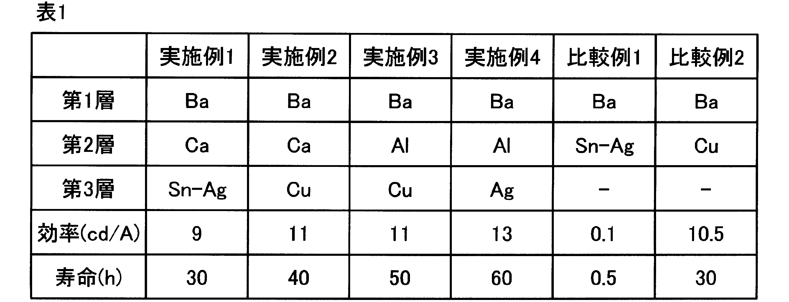
また、実施例2、実施例3及び比較例2を参照すれば明らかな通り、Baの第1層、Ca又はAlの第2層、及びCuの第3層の3層からなる陰極を使用すると、かかる第2層を省略しBaの層及びCuの層の2層のみからなる陰極を使用した場合に比べて、発光効率が優れていた。また、輝度半減寿命も優れていた。
さらに、実施例4に示される通り、Baの第1層及びAlの第2層に加えて第3層としてAgのみからなる層を用いた場合が、発光効率及び輝度半減寿命のいずれにおいても、最も優れていた。
陰極の第1層として3.5nmのLiF層、第2層として4nmのCa層、第3層として15nmのAg層を成膜した他は、実施例1と同様に操作し、発光素子7を得て評価した。結果を表2に示す。なお、第3層の可視光の透過率は40%以上であった。
陰極の第1層として3.5nmのLiF層を成膜し、Ca層を成膜せず第1層上に直接15nmのAg層を成膜した他は、実施例1と同様に操作し、その第2電極が2つの層からなる発光素子8を得て評価した。結果を表2に示す。
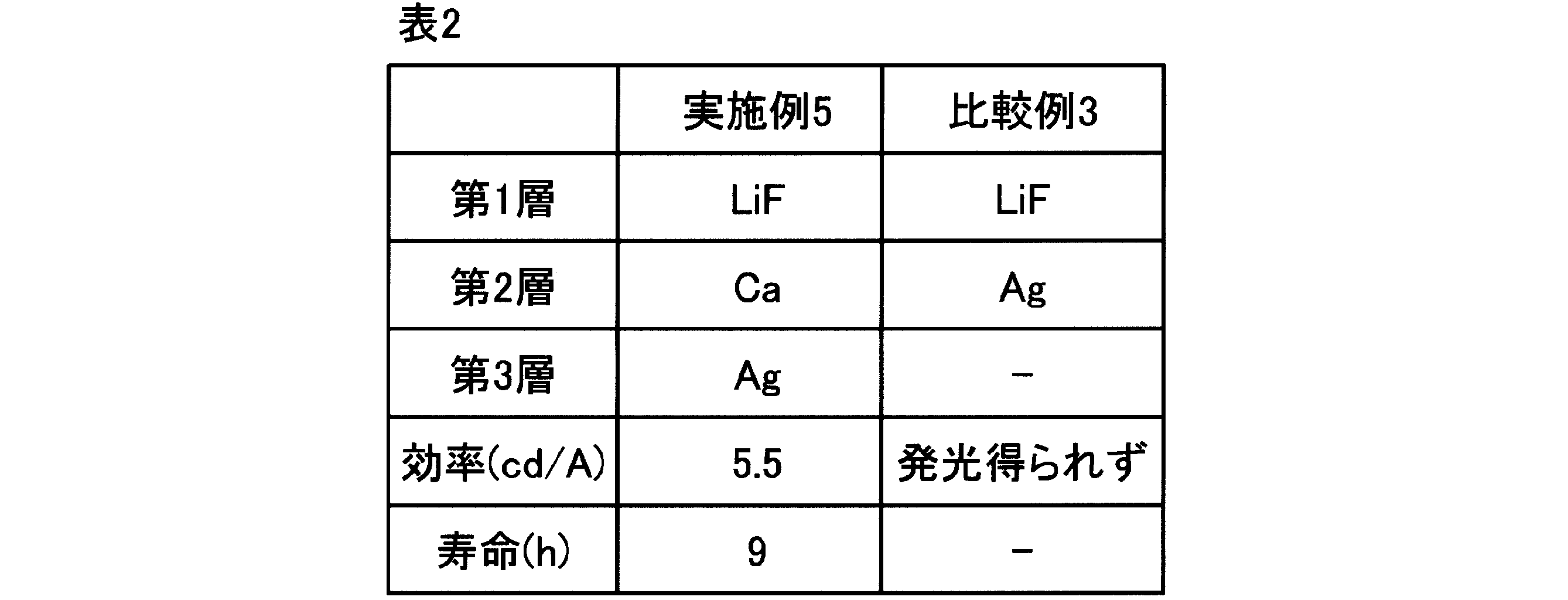
陰極の第1層として3.8nmのNaF層、第2層として共蒸着法を用いて10nmのMg-Ag混合層(混合モル比率、Mg:Ag=2:8)、第3層として5nmのAg層を成膜した他は、実施例1と同様に操作し、発光素子9を得て評価した。結果を表3に示す。なお、第3層の可視光の透過率は40%以上であった。
陰極の第1層として3.8nmのNaF層、第2層として共蒸着法を用いて10nmのMg-Ag混合層(混合モル比率、Mg:Ag=3:7)、第3層として5nmのAg層を成膜した他は、実施例1と同様に操作し、発光素子10を得て評価した。結果を表3に示す。なお、第3層の可視光の透過率は40%以上であった。
陰極の第1層として3.8nmのNaF層、第2層として共蒸着法を用いて10nmのMg-Ag混合層(混合モル比率、Mg:Ag=5:5)、第3層として5nmのAg層を成膜した他は、実施例1と同様に操作し、発光素子11を得て評価した。結果を表3に示す。なお、第3層の可視光の透過率は40%以上であった。
陰極の第1層として3.8nmのNaF層、第2層として共蒸着法を用いて10nmのMg-Ag混合層(混合モル比率、Mg:Ag=8:2)、第3層として5nmのAg層を成膜した他は、実施例1と同様に操作し、発光素子12を得て評価した。結果を表3に示す。なお、第3層の可視光の透過率は40%以上であった。
陰極の第1層として3.8nmのNaF層を成膜し、Mg-Ag混合層を成膜せず、第1層上に直接15nmのAg層を成膜した他は、実施例1と同様に操作し、その第2電極が2つの層からなる発光素子13を得て評価した。結果を表3に示す。

また、実施例6~9を参照すれば明らかな通り、陰極の第1層としてNaFを用いた場合、陰極の第2層として用いたMg-Ag混合層のMgモル割合が20%~30%である実施例6および7は、かかるMgモル割合が50%以上の実施例8および9に較べて、発光効率および輝度半減寿命が優れていた。
また、表3を参照すれば明らかな通り、陰極の第1層としてNaFを用いた実施例6~9は、かかる陰極第1層としてBaを用いた実施例4と比較して、駆動電圧が低く、消費電力の観点で優れていた。
(2-1:陽極及びバッファ層の形成)
ガラス基板上に、真空蒸着法にて、第一電極である厚さ100nmの銀層を成膜した。本銀層は反射率90%の光反射陽極である。さらに、真空を保ったまま、光反射陽極上に、正孔注入層として、厚さ10nmのMoO3層をさらに成膜した。
正孔輸送性高分子材料及びキシレンを0.7重量%の割合で混合し、正孔輸送層形成用組成物を得た。ここで下記式(2)で示される正孔輸送性高分子材料は、国際公開第2005/52027号パンフレットにおいて、P1として例示される下記化合物を用いた。該正孔輸送性高分子材料は国際公開第2005/52027号パンフレットのScheme1の方法を用いて製造した。

この塗膜を設けた基板を190℃で20分間加熱し、塗膜を不溶化させた後、室温まで自然冷却させ、正孔輸送層を得た。
発光高分子材料及びキシレンを1.3重量%の割合で混合し、発光層形成用組成物を得た。ここで発光高分子材料は、サメイション(株)製Lumation GP1300を用いた。
上記(2-3)で得た、陽極、正孔注入層、正孔輸送層及び発光層を有する基板の発光層の上に、真空蒸着法によって、第二電極の第1層である5nmのBa層、第2層である1.5nmのAl層、第3層である15nmのAg層を、連続的に成膜し、第1層~第3層からなる陰極を形成した。なお、第3層の可視光の透過率は40%以上であった。
上記(2-4)で得た、積層を有する基板を真空蒸着装置より取り出し、窒素雰囲気下で、封止ガラス及び2液混合エポキシ樹脂にて封止し、発光素子14を得た。
上記(2-5)で得られた素子を実施例1と同様に評価した。結果を表4に示す。
陰極の第1層として3nmのNaF層、第2層として共蒸着法を用いて10nmのMg-Ag混合層(混合モル比率、Mg:Ag=3:7)、第3層として5nmのAg層を成膜した他は、実施例10と同様に操作し、発光素子15を得て評価した。結果を表4に示す。なお、第3層の可視光の透過率は40%以上であった。
陰極の第1層として5nmのBa層を成膜し、Al層を成膜せず、第1層上に直接15nmのAg層を成膜した他は、実施例10と同様に操作し、その第2電極が2つの層からなる発光素子16を得て評価した。結果を表4に示す。
陰極の第1層として3.8nmのNaF層を成膜し、Mg-Ag混合層を成膜せず、第1層上に直接15nmのAg層を成膜した他は、実施例10と同様に操作し、その第2電極が2つの層からなる発光素子17を得て評価した。結果を表4に示す。
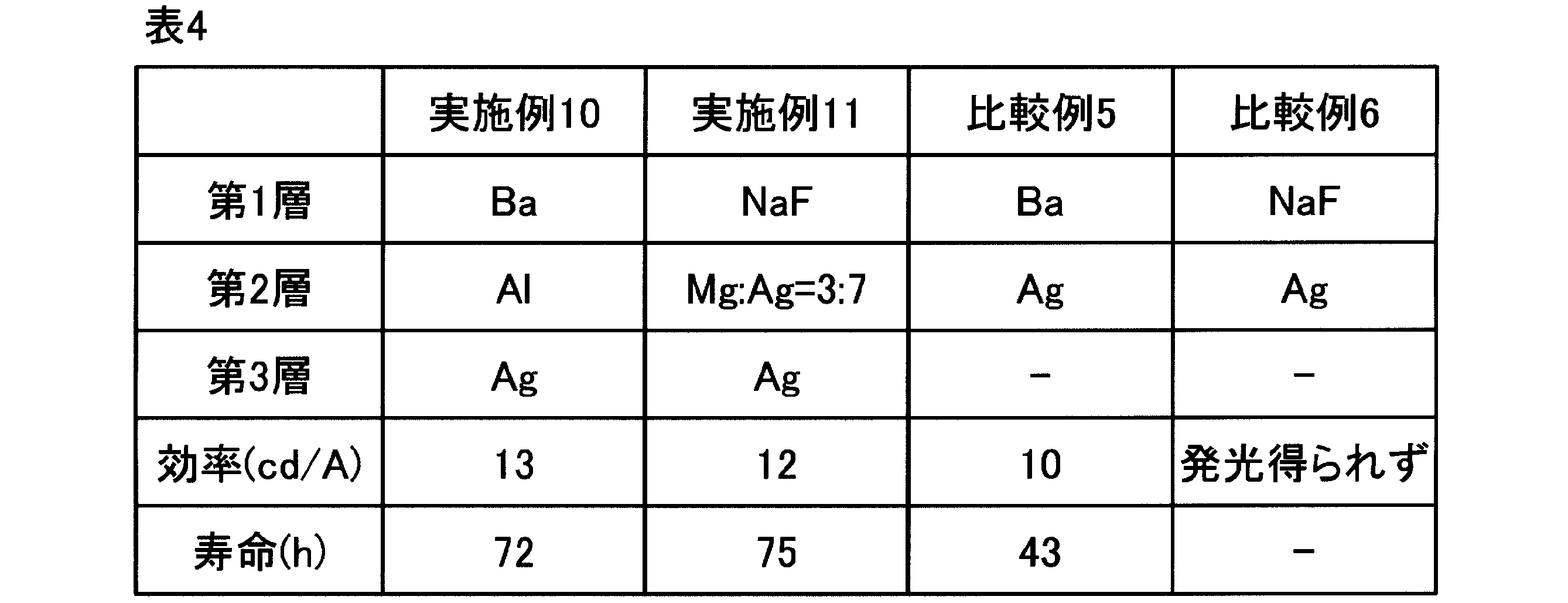
実施例11と比較例6を参照すれば明らかな通り、陰極の第1層としてNaFを用いた場合、陰極の第2層としてMg-Ag混合層を使用すると、かかる第2層を省略した比較例6では電界発光が得られない結果に対して、発光特性が顕著に優れていた。
Claims (18)
- 第一電極、第二電極、及び前記第一電極と第二電極との間に設けられ高分子化合物を含む発光層を有する高分子発光素子であって、
前記第二電極が前記発光層側から順に、第1層、第2層及び第3層の3層からなり、
前記第2層に含まれる材料の少なくとも1種類が前記第1層に含まれる材料の少なくとも1種類に対して還元作用を有し、且つ前記第3層の可視光の透過率が40%以上であることを特徴とする高分子発光素子。 - 前記第2層に含まれる材料の全種類がそれぞれ前記第1層に含まれる材料の全種類に対して還元作用を有する、請求項1に記載の高分子発光素子。
- 前記第1層が金属、金属酸化物、金属フッ化物、及びこれらの混合物からなる群より選択される材料を含む、請求項1に記載の高分子発光素子。
- 前記第2層が、カルシウム、アルミニウム、マグネシウム、及びこれらの混合物からなる群より選択される金属を含む、請求項1に記載の高分子発光素子。
- 前記第1層が、アルカリ金属、アルカリ土類金属、アルカリ金属の酸化物、アルカリ土類金属の酸化物、アルカリ金属のフッ化物、アルカリ土類金属のフッ化物、及びこれらの混合物からなる群より選択される材料を含む、請求項1に記載の高分子発光素子。
- 第一電極、第二電極、及び前記第一電極と第二電極との間に設けられ高分子化合物を含む発光層を有する高分子発光素子であって、
前記第二電極が前記発光層側から順に、第1層、第2層及び第3層の3層からなり、
前記第1層が金属、金属酸化物、金属フッ化物、及びこれらの混合物からなる群より選択される材料を含み、
前記第2層がカルシウム、アルミニウム、マグネシウム、及びこれらの混合物からなる
群より選択される金属を含み、且つ、
前記第3層の可視光の透過率が40%以上であることを特徴とする高分子発光素子。 - 前記第1層が金属酸化物および/または金属フッ化物を含み、前記第2層に含まれる材料が、前記第1層に含まれる材料に対する還元剤である請求項6に記載の高分子発光素子。
- 前記第1層が金属を含み、前記第2層に含まれる材料が、前記第1層に含まれる金属の酸化物に対する還元剤である請求項7に記載の高分子発光素子。
- 前記第1層が、アルカリ金属、アルカリ土類金属、アルカリ金属の酸化物、アルカリ土類金属の酸化物、アルカリ金属のフッ化物、アルカリ土類金属のフッ化物、及びこれらの混合物からなる群より選択される材料を含む、請求項6に記載の高分子発光素子。
- 前記第1層がバリウム、酸化バリウム、フッ化バリウム、及びこれらの混合物からなる群より選択される材料を含む請求項9に記載の高分子発光素子。
- 前記第1層がナトリウム、酸化ナトリウム、フッ化ナトリウム、及びこれらの混合物からなる群より選択される材料を含む請求項9に記載の高分子発光素子。
- 前記第1層がルビジウム、酸化ルビジウム、フッ化ルビジウム、及びこれらの混合物からなる群より選択される材料を含む請求項9に記載の高分子発光素子。
- 前記第3層が、金、銀、銅、錫、鉛、ニッケル、インジウム、及びこれらの合金からなる群より選択される材料からなり、その膜厚が5nm以上30nm以下である請求項1または6に記載の高分子発光素子。
- 前記第一電極の可視光に対する反射率が80%以上である請求項1または6に記載の高分子発光素子。
- 請求項1または6に記載の高分子発光素子の製造方法であって、
基板上に第一電極を設ける工程、
第一電極の上に発光層を設ける工程、及び
発光層の上に第二電極を設ける工程を含み、
前記第二電極を設ける工程が、
発光層の上に第1層を設ける工程、
第1層の上に第2層を設ける工程、及び
第2層の上に第3層を設ける工程を含むことを特徴とする製造方法。 - 前記発光層の上に第1層を設ける工程、第1層の上に第2層を設ける工程、及び第2層の上に第3層を設ける工程を、真空蒸着法により行なう請求項15に記載の製造方法。
- 請求項1または6に記載の高分子発光素子を1画素単位として備える高分子発光ディスプレイ装置。
- 請求項1または6に記載の高分子発光素子を有する面状光源。
Priority Applications (3)
| Application Number | Priority Date | Filing Date | Title |
|---|---|---|---|
| CN2008801227299A CN101911833A (zh) | 2007-12-28 | 2008-12-25 | 高分子发光元件、制造方法以及高分子发光显示装置 |
| EP08868190.3A EP2234459B1 (en) | 2007-12-28 | 2008-12-25 | Polymer light-emitting device, method for manufacturing the same and polymer light-emitting display device |
| US12/810,778 US8895961B2 (en) | 2007-12-28 | 2008-12-25 | Polymer light emitting element, method for manufacturing the same and polymer light emitting display device |
Applications Claiming Priority (2)
| Application Number | Priority Date | Filing Date | Title |
|---|---|---|---|
| JP2007341228 | 2007-12-28 | ||
| JP2007-341228 | 2007-12-28 |
Publications (1)
| Publication Number | Publication Date |
|---|---|
| WO2009084590A1 true WO2009084590A1 (ja) | 2009-07-09 |
Family
ID=40824304
Family Applications (1)
| Application Number | Title | Priority Date | Filing Date |
|---|---|---|---|
| PCT/JP2008/073610 WO2009084590A1 (ja) | 2007-12-28 | 2008-12-25 | 高分子発光素子、製造方法及び高分子発光ディスプレイ装置 |
Country Status (7)
| Country | Link |
|---|---|
| US (1) | US8895961B2 (ja) |
| EP (1) | EP2234459B1 (ja) |
| JP (1) | JP2009176730A (ja) |
| KR (1) | KR20100106426A (ja) |
| CN (1) | CN101911833A (ja) |
| TW (1) | TWI578850B (ja) |
| WO (1) | WO2009084590A1 (ja) |
Cited By (6)
| Publication number | Priority date | Publication date | Assignee | Title |
|---|---|---|---|---|
| CN101710612A (zh) * | 2009-11-13 | 2010-05-19 | 清华大学 | 一种有机电致发光器件 |
| JP2010146895A (ja) * | 2008-12-19 | 2010-07-01 | Sumitomo Chemical Co Ltd | 有機エレクトロルミネッセンス素子 |
| CN101916830A (zh) * | 2010-07-14 | 2010-12-15 | 中国科学院长春应用化学研究所 | 白色有机电致发光器件及其制备方法 |
| CN102714902A (zh) * | 2010-01-15 | 2012-10-03 | 住友化学株式会社 | 高分子发光元件 |
| JP2014049696A (ja) * | 2012-09-03 | 2014-03-17 | Nippon Hoso Kyokai <Nhk> | 有機電界発光素子 |
| CN105489779A (zh) * | 2014-10-01 | 2016-04-13 | 三星显示有限公司 | 有机发光元件以及包含该有机发光元件的有机发光装置 |
Families Citing this family (10)
| Publication number | Priority date | Publication date | Assignee | Title |
|---|---|---|---|---|
| KR20110038513A (ko) * | 2009-10-08 | 2011-04-14 | 삼성모바일디스플레이주식회사 | 유기 발광 표시 장치 및 그 제조 방법 |
| JP2011165653A (ja) * | 2010-01-14 | 2011-08-25 | Canon Inc | 有機el素子およびそれを用いた発光装置 |
| CN102447072A (zh) * | 2010-10-12 | 2012-05-09 | 西安文景光电科技有限公司 | 铝与氧化钼共混薄膜作为阳极的有机电致发光器件 |
| JP5969216B2 (ja) * | 2011-02-11 | 2016-08-17 | 株式会社半導体エネルギー研究所 | 発光素子、表示装置、照明装置、及びこれらの作製方法 |
| JP5939564B2 (ja) * | 2012-02-06 | 2016-06-22 | 株式会社Joled | 有機el素子の製造方法 |
| CN103296217A (zh) * | 2012-02-29 | 2013-09-11 | 海洋王照明科技股份有限公司 | 有机电致发光器件及其制备方法 |
| JP6945983B2 (ja) * | 2016-10-06 | 2021-10-06 | 住友化学株式会社 | 有機elデバイス、表示素子及び有機elデバイスの製造方法 |
| CN108281565A (zh) * | 2017-01-05 | 2018-07-13 | 昆山工研院新型平板显示技术中心有限公司 | 一种电极及应用其的有机电致发光器件 |
| CN108281562B (zh) | 2017-01-05 | 2020-06-19 | 昆山工研院新型平板显示技术中心有限公司 | 一种电极及应用其的有机电致发光器件 |
| CN114068826A (zh) * | 2020-08-03 | 2022-02-18 | 湖南鼎一致远科技发展有限公司 | 一种空穴传输层和色带及其制备方法 |
Citations (62)
| Publication number | Priority date | Publication date | Assignee | Title |
|---|---|---|---|---|
| JPS5751781A (en) | 1980-07-17 | 1982-03-26 | Eastman Kodak Co | Organic electroluminiscent cell and method |
| JPS59194393A (ja) | 1983-03-25 | 1984-11-05 | イ−ストマン コダツク カンパニ− | 改良された電力転換効率をもつ有機エレクトロルミネツセント装置 |
| JPS6370257A (ja) | 1986-09-12 | 1988-03-30 | Fuji Xerox Co Ltd | 電子写真用電荷輸送材料 |
| JPH02135359A (ja) | 1988-11-16 | 1990-05-24 | Fuji Xerox Co Ltd | 電子写真感光体 |
| JPH02135361A (ja) | 1988-11-16 | 1990-05-24 | Fuji Xerox Co Ltd | 電子写真感光体 |
| JPH02209988A (ja) | 1989-02-10 | 1990-08-21 | Idemitsu Kosan Co Ltd | 薄膜エレクトロルミネッセンス素子 |
| JPH0337992A (ja) | 1989-07-04 | 1991-02-19 | Idemitsu Kosan Co Ltd | 有機エレクトロルミネッセンス素子の製造方法 |
| JPH03152184A (ja) | 1989-11-08 | 1991-06-28 | Nec Corp | 有機薄膜el素子 |
| JPH05263073A (ja) | 1992-03-17 | 1993-10-12 | Sumitomo Chem Co Ltd | 有機エレクトロルミネッセンス素子 |
| JPH061972A (ja) | 1991-06-05 | 1994-01-11 | Sumitomo Chem Co Ltd | 有機エレクトロルミネッセンス素子 |
| WO1995007955A1 (de) | 1993-09-15 | 1995-03-23 | Hoechst Aktiengesellschaft | Verwendung von polymeren mit isolierten chromophoren als elektrolumineszenzmaterialien |
| WO1996010617A1 (de) | 1994-09-30 | 1996-04-11 | Hoechst Aktiengesellschaft | Poly(paraphenylenvinylen)-derivate und ihre verwendung als elektrolumineszenzmaterialien |
| EP0707020A2 (de) | 1994-10-14 | 1996-04-17 | Hoechst Aktiengesellschaft | Konjugierte Polymere mit Spirozentren und ihre Verwendung als Elektrolumineszenzmaterialien |
| WO1996029356A2 (de) | 1995-03-20 | 1996-09-26 | Hoechst Aktiengesellschaft | OLIGO-p-PHENYLEN-EINHEITEN ENTHALTENDE POLYMERE, VERFAHREN ZU IHRER HERSTELLUNG SOWIE IHRE VERWENDUNG |
| WO1997005184A1 (en) | 1995-07-28 | 1997-02-13 | The Dow Chemical Company | 2,7-aryl-9-substituted fluorenes and 9-substituted fluorene oligomers and polymers |
| JPH0945478A (ja) | 1995-02-01 | 1997-02-14 | Sumitomo Chem Co Ltd | 高分子蛍光体とその製造方法および有機エレクトロルミネッセンス素子 |
| WO1997009394A1 (de) | 1995-09-04 | 1997-03-13 | Hoechst Research & Technology Deutschland Gmbh & Co. Kg | Polymere mit triarylamin-einheiten als elektrolumineszenzmaterialien |
| JPH09111233A (ja) | 1995-10-16 | 1997-04-28 | Sumitomo Chem Co Ltd | 高分子蛍光体、その製造方法及び有機エレクトロルミネッセンス素子 |
| WO1998006773A1 (en) | 1996-08-13 | 1998-02-19 | The Dow Chemical Company | Poly(arylamines) and films thereof |
| US5741921A (en) | 1994-11-25 | 1998-04-21 | Hoechst Aktiengesellschaft | Conjugated polymers containing hetero-spiro atoms and their use as electroluminescence materials |
| JPH10114891A (ja) | 1996-08-21 | 1998-05-06 | Sumitomo Chem Co Ltd | 高分子蛍光体および有機エレクトロルミネッセンス素子 |
| WO1998021262A1 (de) | 1996-11-13 | 1998-05-22 | Aventis Research & Technologies Gmbh & Co Kg | Geordnete poly(arylenvinylen)-terpolymere, verfahren zu ihrer herstellung und ihre verwendung als elektrolumineszenzmaterialien |
| WO1998027136A1 (de) | 1996-12-16 | 1998-06-25 | Aventis Research & Technologies Gmbh & Co Kg | ARYLSUBSTITUIERTE POLY(p-ARYLENVINYLENE), VERFAHREN ZUR HERSTELLUNG UND DEREN VERWENDUNG IN ELEKTROLUMINESZENZBAUELEMENTEN |
| US5777070A (en) | 1997-10-23 | 1998-07-07 | The Dow Chemical Company | Process for preparing conjugated polymers |
| JPH10324870A (ja) | 1997-05-23 | 1998-12-08 | Sumitomo Chem Co Ltd | 高分子蛍光体および有機エレクトロルミネッセンス素子 |
| WO1999013692A1 (en) | 1997-09-05 | 1999-03-18 | Cambridge Display Technology Limited | SELF-ASSEMBLED TRANSPORT LAYERS FOR OLEDs |
| WO1999024526A1 (de) | 1997-11-05 | 1999-05-20 | Axiva Gmbh | Substituierte poly(arylenvinylene), verfahren zur herstellung und deren verwendung in elektrolumineszenzelementen |
| WO1999048160A1 (en) | 1998-03-13 | 1999-09-23 | Cambridge Display Technology Ltd. | Electroluminescent devices |
| WO1999054385A1 (en) | 1998-04-21 | 1999-10-28 | The Dow Chemical Company | Fluorene-containing polymers and electroluminescent devices therefrom |
| WO1999054943A1 (en) | 1998-04-21 | 1999-10-28 | The Dow Chemical Company | Organic electroluminescent devices with improved stability in air |
| WO2000006665A1 (en) | 1998-07-28 | 2000-02-10 | The Dow Chemical Company | Organic electroluminescent devices |
| GB2340304A (en) | 1998-08-21 | 2000-02-16 | Cambridge Display Tech Ltd | Organic light emitters |
| JP2000068065A (ja) * | 1998-08-13 | 2000-03-03 | Tdk Corp | 有機el素子 |
| JP2000080167A (ja) | 1997-07-22 | 2000-03-21 | Sumitomo Chem Co Ltd | 正孔輸送性高分子とその製造方法および有機エレクトロルミネッセンス素子 |
| JP2000104057A (ja) | 1998-07-27 | 2000-04-11 | Sumitomo Chem Co Ltd | 高分子蛍光体および高分子発光素子 |
| WO2000022026A1 (de) | 1998-10-10 | 2000-04-20 | Celanese Ventures Gmbh | Konjugierte polymere, enthaltend spezielle fluoren-bausteine mit verbesserten eigenschaften |
| WO2000022027A1 (de) | 1998-10-10 | 2000-04-20 | Celanese Ventures Gmbh | Konjugierte polymere enthaltend 2,7-fluorenyleinheiten mit verbesserten eigenschaften |
| JP2000136379A (ja) | 1998-06-10 | 2000-05-16 | Sumitomo Chem Co Ltd | 高分子蛍光体および有機エレクトロルミネッセンス素子 |
| WO2000035987A1 (de) | 1998-12-15 | 2000-06-22 | Celanese Ventures Gmbh | Verfahren zur herstellung von derivaten des polyarylenvinylen |
| WO2000046321A1 (en) | 1999-02-04 | 2000-08-10 | The Dow Chemical Company | Fluorene copolymers and devices made therefrom |
| JP2000252065A (ja) | 1999-02-25 | 2000-09-14 | Sumitomo Chem Co Ltd | 高分子発光素子 |
| WO2000053656A1 (en) | 1999-03-05 | 2000-09-14 | Cambridge Display Technology Limited | Polymer preparation |
| WO2000053655A1 (de) | 1998-02-13 | 2000-09-14 | Celanese Ventures Gmbh | Triptycen-polymere und -copolymere |
| WO2000055927A1 (en) | 1999-03-12 | 2000-09-21 | Cambridge Display Technology Limited | Polymers, their preparation and uses |
| GB2348316A (en) | 1999-03-26 | 2000-09-27 | Cambridge Display Tech Ltd | Organic opto-electronic device |
| JP2000299189A (ja) | 1999-02-09 | 2000-10-24 | Sumitomo Chem Co Ltd | 高分子発光素子ならびにそれを用いた表示装置および面状光源 |
| JP2000303066A (ja) | 1999-04-21 | 2000-10-31 | Sumitomo Chem Co Ltd | 高分子蛍光体およびそれを用いた高分子発光素子 |
| JP2000351967A (ja) | 1999-04-09 | 2000-12-19 | Sumitomo Chem Co Ltd | 高分子蛍光体およびそれを用いた高分子発光素子 |
| JP2001003045A (ja) | 1999-04-21 | 2001-01-09 | Sumitomo Chem Co Ltd | 高分子蛍光体およびそれを用いた高分子発光素子 |
| WO2001019834A1 (en) | 1999-09-16 | 2001-03-22 | Cambridge Display Technology Limited | Preparation of benzenediboronic acid via a disilylated aryl-intermediate |
| JP2001123156A (ja) | 1999-08-03 | 2001-05-08 | Sumitomo Chem Co Ltd | 高分子蛍光体およびそれを用いた高分子発光素子 |
| WO2001034722A1 (de) | 1999-11-09 | 2001-05-17 | Covion Organic Semiconductors Gmbh | Substituierte poly(arylenvinylene), verfahren zur herstellung und deren verwendung in elektrolumineszenzvorrichtungen |
| JP2001181618A (ja) | 1999-12-27 | 2001-07-03 | Sumitomo Chem Co Ltd | 高分子蛍光体の製造方法および高分子発光素子 |
| JP2004079422A (ja) | 2002-08-21 | 2004-03-11 | Tdk Corp | 有機el素子 |
| JP2005135624A (ja) * | 2003-10-28 | 2005-05-26 | Sharp Corp | 有機el素子 |
| WO2005052027A1 (en) | 2003-11-17 | 2005-06-09 | Sumitomo Chemical Company, Limited | Crosslinkable arylamine compounds and conjugated oligomers of polymers based thereon |
| WO2006049579A1 (en) * | 2004-11-01 | 2006-05-11 | Agency For Science, Technology And Research | Poly(arylenevinylene) and poly(heteroarylenevinylene) light emitting polymers and polymer light-emitting devices |
| JP2006186317A (ja) * | 2004-11-11 | 2006-07-13 | Samsung Electronics Co Ltd | 多層構造のナノ結晶およびその製造方法 |
| JP2007129170A (ja) * | 2005-11-07 | 2007-05-24 | Mitsubishi Chemicals Corp | アルカリ金属原子及びフラーレン類を含有する層を有する有機電界発光素子及びその製造方法 |
| JP2007265792A (ja) * | 2006-03-28 | 2007-10-11 | Dainippon Printing Co Ltd | 有機エレクトロルミネッセンス素子 |
| JP2007329054A (ja) * | 2006-06-08 | 2007-12-20 | Toppoly Optoelectronics Corp | 画像表示装置 |
| JP2008041692A (ja) * | 2006-08-01 | 2008-02-21 | Matsushita Electric Ind Co Ltd | 有機エレクトロルミネッセント素子およびその製造方法 |
Family Cites Families (21)
| Publication number | Priority date | Publication date | Assignee | Title |
|---|---|---|---|---|
| DE69729394T2 (de) | 1996-11-29 | 2005-06-02 | Idemitsu Kosan Co. Ltd. | Organische elektrolumineszente Vorrichtung |
| US7226966B2 (en) * | 2001-08-03 | 2007-06-05 | Nanogram Corporation | Structures incorporating polymer-inorganic particle blends |
| JP2001338755A (ja) * | 2000-03-21 | 2001-12-07 | Seiko Epson Corp | 有機el素子およびその製造方法 |
| TW515223B (en) * | 2000-07-24 | 2002-12-21 | Tdk Corp | Light emitting device |
| JP4060113B2 (ja) * | 2002-04-05 | 2008-03-12 | 株式会社半導体エネルギー研究所 | 発光装置 |
| CN1320022C (zh) * | 2002-12-25 | 2007-06-06 | 株式会社半导体能源研究所 | 高分子化合物、电致发光元件及发光装置 |
| JP2004292436A (ja) * | 2003-03-07 | 2004-10-21 | Dainippon Printing Co Ltd | 有機化合物、及び有機エレクトロルミネッセンス素子 |
| EP1607392A1 (en) * | 2003-03-17 | 2005-12-21 | Hirose Engineering Co., Ltd. | Blue light-emitting compound, method for producing same and light-emitting device utilizing same |
| JP2004311403A (ja) | 2003-03-27 | 2004-11-04 | Seiko Epson Corp | エレクトロルミネセンス素子及びその製造方法 |
| JP4526776B2 (ja) * | 2003-04-02 | 2010-08-18 | 株式会社半導体エネルギー研究所 | 発光装置及び電子機器 |
| US7429822B2 (en) | 2003-10-28 | 2008-09-30 | Sharp Kabushiki Kaisha | Organic electroluminescence device having a cathode with a metal layer that includes a first metal and a low work function metal |
| JP4366686B2 (ja) | 2003-10-29 | 2009-11-18 | 富士電機ホールディングス株式会社 | 有機el素子の製造方法 |
| JP2005140275A (ja) | 2003-11-07 | 2005-06-02 | Nsk Ltd | プラネタリギヤ装置 |
| EP1712109A4 (en) | 2003-12-30 | 2008-03-19 | Agency Science Tech & Res | FLEXIBLE ELECTROLUMINESCENT DEVICES |
| US7202504B2 (en) * | 2004-05-20 | 2007-04-10 | Semiconductor Energy Laboratory Co., Ltd. | Light-emitting element and display device |
| EP1753839B1 (en) * | 2004-05-21 | 2011-07-20 | Showa Denko K.K. | Polymer light-emitting material and organic light emitting element |
| US20060199035A1 (en) * | 2005-03-02 | 2006-09-07 | Osram Opto Semiconductors Gmbh & Co. | Organic electroluminescent device |
| JP5017820B2 (ja) * | 2005-09-01 | 2012-09-05 | 大日本印刷株式会社 | エレクトロルミネッセンス素子およびその製造方法 |
| KR100645707B1 (ko) * | 2006-01-27 | 2006-11-15 | 삼성에스디아이 주식회사 | 유기전계발광 표시장치 및 그 제조방법 |
| US20070290604A1 (en) | 2006-06-16 | 2007-12-20 | Matsushita Electric Industrial Co., Ltd. | Organic electroluminescent device and method of producing the same |
| JP5326093B2 (ja) * | 2006-11-22 | 2013-10-30 | 日本電気株式会社 | 半導体装置及びその製造方法 |
-
2008
- 2008-12-25 JP JP2008330525A patent/JP2009176730A/ja active Pending
- 2008-12-25 WO PCT/JP2008/073610 patent/WO2009084590A1/ja active Application Filing
- 2008-12-25 EP EP08868190.3A patent/EP2234459B1/en not_active Not-in-force
- 2008-12-25 CN CN2008801227299A patent/CN101911833A/zh active Pending
- 2008-12-25 US US12/810,778 patent/US8895961B2/en active Active
- 2008-12-25 KR KR1020107014078A patent/KR20100106426A/ko not_active Application Discontinuation
- 2008-12-25 TW TW097150759A patent/TWI578850B/zh not_active IP Right Cessation
Patent Citations (63)
| Publication number | Priority date | Publication date | Assignee | Title |
|---|---|---|---|---|
| JPS5751781A (en) | 1980-07-17 | 1982-03-26 | Eastman Kodak Co | Organic electroluminiscent cell and method |
| JPS59194393A (ja) | 1983-03-25 | 1984-11-05 | イ−ストマン コダツク カンパニ− | 改良された電力転換効率をもつ有機エレクトロルミネツセント装置 |
| JPS6370257A (ja) | 1986-09-12 | 1988-03-30 | Fuji Xerox Co Ltd | 電子写真用電荷輸送材料 |
| JPH02135359A (ja) | 1988-11-16 | 1990-05-24 | Fuji Xerox Co Ltd | 電子写真感光体 |
| JPH02135361A (ja) | 1988-11-16 | 1990-05-24 | Fuji Xerox Co Ltd | 電子写真感光体 |
| JPH02209988A (ja) | 1989-02-10 | 1990-08-21 | Idemitsu Kosan Co Ltd | 薄膜エレクトロルミネッセンス素子 |
| JPH0337992A (ja) | 1989-07-04 | 1991-02-19 | Idemitsu Kosan Co Ltd | 有機エレクトロルミネッセンス素子の製造方法 |
| JPH03152184A (ja) | 1989-11-08 | 1991-06-28 | Nec Corp | 有機薄膜el素子 |
| JPH061972A (ja) | 1991-06-05 | 1994-01-11 | Sumitomo Chem Co Ltd | 有機エレクトロルミネッセンス素子 |
| JPH05263073A (ja) | 1992-03-17 | 1993-10-12 | Sumitomo Chem Co Ltd | 有機エレクトロルミネッセンス素子 |
| WO1995007955A1 (de) | 1993-09-15 | 1995-03-23 | Hoechst Aktiengesellschaft | Verwendung von polymeren mit isolierten chromophoren als elektrolumineszenzmaterialien |
| WO1996010617A1 (de) | 1994-09-30 | 1996-04-11 | Hoechst Aktiengesellschaft | Poly(paraphenylenvinylen)-derivate und ihre verwendung als elektrolumineszenzmaterialien |
| EP0707020A2 (de) | 1994-10-14 | 1996-04-17 | Hoechst Aktiengesellschaft | Konjugierte Polymere mit Spirozentren und ihre Verwendung als Elektrolumineszenzmaterialien |
| US5741921A (en) | 1994-11-25 | 1998-04-21 | Hoechst Aktiengesellschaft | Conjugated polymers containing hetero-spiro atoms and their use as electroluminescence materials |
| JPH0945478A (ja) | 1995-02-01 | 1997-02-14 | Sumitomo Chem Co Ltd | 高分子蛍光体とその製造方法および有機エレクトロルミネッセンス素子 |
| WO1996029356A2 (de) | 1995-03-20 | 1996-09-26 | Hoechst Aktiengesellschaft | OLIGO-p-PHENYLEN-EINHEITEN ENTHALTENDE POLYMERE, VERFAHREN ZU IHRER HERSTELLUNG SOWIE IHRE VERWENDUNG |
| WO1997005184A1 (en) | 1995-07-28 | 1997-02-13 | The Dow Chemical Company | 2,7-aryl-9-substituted fluorenes and 9-substituted fluorene oligomers and polymers |
| WO1997009394A1 (de) | 1995-09-04 | 1997-03-13 | Hoechst Research & Technology Deutschland Gmbh & Co. Kg | Polymere mit triarylamin-einheiten als elektrolumineszenzmaterialien |
| JPH09111233A (ja) | 1995-10-16 | 1997-04-28 | Sumitomo Chem Co Ltd | 高分子蛍光体、その製造方法及び有機エレクトロルミネッセンス素子 |
| WO1998006773A1 (en) | 1996-08-13 | 1998-02-19 | The Dow Chemical Company | Poly(arylamines) and films thereof |
| JPH10114891A (ja) | 1996-08-21 | 1998-05-06 | Sumitomo Chem Co Ltd | 高分子蛍光体および有機エレクトロルミネッセンス素子 |
| WO1998021262A1 (de) | 1996-11-13 | 1998-05-22 | Aventis Research & Technologies Gmbh & Co Kg | Geordnete poly(arylenvinylen)-terpolymere, verfahren zu ihrer herstellung und ihre verwendung als elektrolumineszenzmaterialien |
| WO1998027136A1 (de) | 1996-12-16 | 1998-06-25 | Aventis Research & Technologies Gmbh & Co Kg | ARYLSUBSTITUIERTE POLY(p-ARYLENVINYLENE), VERFAHREN ZUR HERSTELLUNG UND DEREN VERWENDUNG IN ELEKTROLUMINESZENZBAUELEMENTEN |
| JPH10324870A (ja) | 1997-05-23 | 1998-12-08 | Sumitomo Chem Co Ltd | 高分子蛍光体および有機エレクトロルミネッセンス素子 |
| JP2000080167A (ja) | 1997-07-22 | 2000-03-21 | Sumitomo Chem Co Ltd | 正孔輸送性高分子とその製造方法および有機エレクトロルミネッセンス素子 |
| WO1999013692A1 (en) | 1997-09-05 | 1999-03-18 | Cambridge Display Technology Limited | SELF-ASSEMBLED TRANSPORT LAYERS FOR OLEDs |
| US5777070A (en) | 1997-10-23 | 1998-07-07 | The Dow Chemical Company | Process for preparing conjugated polymers |
| WO1999024526A1 (de) | 1997-11-05 | 1999-05-20 | Axiva Gmbh | Substituierte poly(arylenvinylene), verfahren zur herstellung und deren verwendung in elektrolumineszenzelementen |
| WO2000053655A1 (de) | 1998-02-13 | 2000-09-14 | Celanese Ventures Gmbh | Triptycen-polymere und -copolymere |
| JP2006295203A (ja) | 1998-03-13 | 2006-10-26 | Cambridge Display Technol Ltd | エレクトロルミネッセンス素子及びその製造方法 |
| WO1999048160A1 (en) | 1998-03-13 | 1999-09-23 | Cambridge Display Technology Ltd. | Electroluminescent devices |
| WO1999054385A1 (en) | 1998-04-21 | 1999-10-28 | The Dow Chemical Company | Fluorene-containing polymers and electroluminescent devices therefrom |
| WO1999054943A1 (en) | 1998-04-21 | 1999-10-28 | The Dow Chemical Company | Organic electroluminescent devices with improved stability in air |
| JP2000136379A (ja) | 1998-06-10 | 2000-05-16 | Sumitomo Chem Co Ltd | 高分子蛍光体および有機エレクトロルミネッセンス素子 |
| JP2000104057A (ja) | 1998-07-27 | 2000-04-11 | Sumitomo Chem Co Ltd | 高分子蛍光体および高分子発光素子 |
| WO2000006665A1 (en) | 1998-07-28 | 2000-02-10 | The Dow Chemical Company | Organic electroluminescent devices |
| JP2000068065A (ja) * | 1998-08-13 | 2000-03-03 | Tdk Corp | 有機el素子 |
| GB2340304A (en) | 1998-08-21 | 2000-02-16 | Cambridge Display Tech Ltd | Organic light emitters |
| WO2000022027A1 (de) | 1998-10-10 | 2000-04-20 | Celanese Ventures Gmbh | Konjugierte polymere enthaltend 2,7-fluorenyleinheiten mit verbesserten eigenschaften |
| WO2000022026A1 (de) | 1998-10-10 | 2000-04-20 | Celanese Ventures Gmbh | Konjugierte polymere, enthaltend spezielle fluoren-bausteine mit verbesserten eigenschaften |
| WO2000035987A1 (de) | 1998-12-15 | 2000-06-22 | Celanese Ventures Gmbh | Verfahren zur herstellung von derivaten des polyarylenvinylen |
| WO2000046321A1 (en) | 1999-02-04 | 2000-08-10 | The Dow Chemical Company | Fluorene copolymers and devices made therefrom |
| JP2000299189A (ja) | 1999-02-09 | 2000-10-24 | Sumitomo Chem Co Ltd | 高分子発光素子ならびにそれを用いた表示装置および面状光源 |
| JP2000252065A (ja) | 1999-02-25 | 2000-09-14 | Sumitomo Chem Co Ltd | 高分子発光素子 |
| WO2000053656A1 (en) | 1999-03-05 | 2000-09-14 | Cambridge Display Technology Limited | Polymer preparation |
| WO2000055927A1 (en) | 1999-03-12 | 2000-09-21 | Cambridge Display Technology Limited | Polymers, their preparation and uses |
| GB2348316A (en) | 1999-03-26 | 2000-09-27 | Cambridge Display Tech Ltd | Organic opto-electronic device |
| JP2000351967A (ja) | 1999-04-09 | 2000-12-19 | Sumitomo Chem Co Ltd | 高分子蛍光体およびそれを用いた高分子発光素子 |
| JP2001003045A (ja) | 1999-04-21 | 2001-01-09 | Sumitomo Chem Co Ltd | 高分子蛍光体およびそれを用いた高分子発光素子 |
| JP2000303066A (ja) | 1999-04-21 | 2000-10-31 | Sumitomo Chem Co Ltd | 高分子蛍光体およびそれを用いた高分子発光素子 |
| JP2001123156A (ja) | 1999-08-03 | 2001-05-08 | Sumitomo Chem Co Ltd | 高分子蛍光体およびそれを用いた高分子発光素子 |
| WO2001019834A1 (en) | 1999-09-16 | 2001-03-22 | Cambridge Display Technology Limited | Preparation of benzenediboronic acid via a disilylated aryl-intermediate |
| WO2001034722A1 (de) | 1999-11-09 | 2001-05-17 | Covion Organic Semiconductors Gmbh | Substituierte poly(arylenvinylene), verfahren zur herstellung und deren verwendung in elektrolumineszenzvorrichtungen |
| JP2001181618A (ja) | 1999-12-27 | 2001-07-03 | Sumitomo Chem Co Ltd | 高分子蛍光体の製造方法および高分子発光素子 |
| JP2004079422A (ja) | 2002-08-21 | 2004-03-11 | Tdk Corp | 有機el素子 |
| JP2005135624A (ja) * | 2003-10-28 | 2005-05-26 | Sharp Corp | 有機el素子 |
| WO2005052027A1 (en) | 2003-11-17 | 2005-06-09 | Sumitomo Chemical Company, Limited | Crosslinkable arylamine compounds and conjugated oligomers of polymers based thereon |
| WO2006049579A1 (en) * | 2004-11-01 | 2006-05-11 | Agency For Science, Technology And Research | Poly(arylenevinylene) and poly(heteroarylenevinylene) light emitting polymers and polymer light-emitting devices |
| JP2006186317A (ja) * | 2004-11-11 | 2006-07-13 | Samsung Electronics Co Ltd | 多層構造のナノ結晶およびその製造方法 |
| JP2007129170A (ja) * | 2005-11-07 | 2007-05-24 | Mitsubishi Chemicals Corp | アルカリ金属原子及びフラーレン類を含有する層を有する有機電界発光素子及びその製造方法 |
| JP2007265792A (ja) * | 2006-03-28 | 2007-10-11 | Dainippon Printing Co Ltd | 有機エレクトロルミネッセンス素子 |
| JP2007329054A (ja) * | 2006-06-08 | 2007-12-20 | Toppoly Optoelectronics Corp | 画像表示装置 |
| JP2008041692A (ja) * | 2006-08-01 | 2008-02-21 | Matsushita Electric Ind Co Ltd | 有機エレクトロルミネッセント素子およびその製造方法 |
Non-Patent Citations (1)
| Title |
|---|
| See also references of EP2234459A4 |
Cited By (9)
| Publication number | Priority date | Publication date | Assignee | Title |
|---|---|---|---|---|
| JP2010146895A (ja) * | 2008-12-19 | 2010-07-01 | Sumitomo Chemical Co Ltd | 有機エレクトロルミネッセンス素子 |
| CN101710612A (zh) * | 2009-11-13 | 2010-05-19 | 清华大学 | 一种有机电致发光器件 |
| CN101710612B (zh) * | 2009-11-13 | 2013-03-27 | 清华大学 | 一种有机电致发光器件 |
| CN102714902A (zh) * | 2010-01-15 | 2012-10-03 | 住友化学株式会社 | 高分子发光元件 |
| US20130033173A1 (en) * | 2010-01-15 | 2013-02-07 | Sumitomo Chemical Company, Limited | Polymer light emitting element |
| CN101916830A (zh) * | 2010-07-14 | 2010-12-15 | 中国科学院长春应用化学研究所 | 白色有机电致发光器件及其制备方法 |
| JP2014049696A (ja) * | 2012-09-03 | 2014-03-17 | Nippon Hoso Kyokai <Nhk> | 有機電界発光素子 |
| CN105489779A (zh) * | 2014-10-01 | 2016-04-13 | 三星显示有限公司 | 有机发光元件以及包含该有机发光元件的有机发光装置 |
| US10014486B2 (en) | 2014-10-01 | 2018-07-03 | Samsung Display Co., Ltd. | Organic light emitting diode and organic light emitting display device including the same |
Also Published As
| Publication number | Publication date |
|---|---|
| CN101911833A (zh) | 2010-12-08 |
| JP2009176730A (ja) | 2009-08-06 |
| TW200948191A (en) | 2009-11-16 |
| KR20100106426A (ko) | 2010-10-01 |
| EP2234459B1 (en) | 2018-01-31 |
| EP2234459A4 (en) | 2011-07-06 |
| US8895961B2 (en) | 2014-11-25 |
| TWI578850B (zh) | 2017-04-11 |
| US20100270544A1 (en) | 2010-10-28 |
| EP2234459A1 (en) | 2010-09-29 |
Similar Documents
| Publication | Publication Date | Title |
|---|---|---|
| WO2009084590A1 (ja) | 高分子発光素子、製造方法及び高分子発光ディスプレイ装置 | |
| JP5293120B2 (ja) | 有機エレクトロルミネッセンス素子およびその製造方法 | |
| WO2009122876A1 (ja) | 有機エレクトロルミネッセンス素子およびその製造方法 | |
| WO2011013488A1 (ja) | 高分子発光素子 | |
| WO2011087058A1 (ja) | 高分子発光素子 | |
| JPWO2009142030A1 (ja) | 有機エレクトロルミネセンス素子、表示装置及び照明装置 | |
| WO2012029936A1 (ja) | 有機エレクトロルミネッセンス素子及びその製造方法 | |
| JP5672705B2 (ja) | 発光装置およびその製造方法 | |
| JP2009021104A (ja) | 有機発光素子の製造方法 | |
| US9136491B2 (en) | Organic electroluminescent element and method for producing the same | |
| JP5320755B2 (ja) | 有機エレクトロルミネッセンス素子およびその製造方法、面状光源、照明装置ならびに表示装置 | |
| JP5249075B2 (ja) | 有機エレクトロルミネッセンス素子 | |
| JP2009205985A (ja) | 有機エレクトロルミネッセンス素子及びその製造方法 | |
| JP2010146893A (ja) | 有機エレクトロルミネッセンス素子、及びその製造方法 | |
| JP2010146894A (ja) | 有機エレクトロルミネッセンス素子 | |
| JP5410774B2 (ja) | 有機エレクトロルミネッセンス素子 | |
| JP5174577B2 (ja) | 有機エレクトロルミネッセンス素子とその製造方法、照明装置、面状光源、表示装置 | |
| JP2010146895A (ja) | 有機エレクトロルミネッセンス素子 | |
| JP4315755B2 (ja) | 有機el装置 | |
| JP5446472B2 (ja) | 有機エレクトロルミネッセンス素子の製造方法 | |
| JP4916102B2 (ja) | 有機el素子 | |
| JP2010027539A (ja) | 有機エレクトロルミネッセンス素子およびその製造方法 | |
| JP2002352964A (ja) | 有機エレクトロルミネッセンス素子およびその製造方法 | |
| JP2011205080A (ja) | 有機エレクトロルミネッセンス素子 |
Legal Events
| Date | Code | Title | Description |
|---|---|---|---|
| WWE | Wipo information: entry into national phase |
Ref document number: 200880122729.9 Country of ref document: CN |
|
| 121 | Ep: the epo has been informed by wipo that ep was designated in this application |
Ref document number: 08868190 Country of ref document: EP Kind code of ref document: A1 |
|
| ENP | Entry into the national phase |
Ref document number: 20107014078 Country of ref document: KR Kind code of ref document: A |
|
| WWE | Wipo information: entry into national phase |
Ref document number: 12810778 Country of ref document: US |
|
| NENP | Non-entry into the national phase |
Ref country code: DE |
|
| WWE | Wipo information: entry into national phase |
Ref document number: 2008868190 Country of ref document: EP |