KR100814980B1 - 산화물, 규산염 및 인산염의 증기를 이용한 석출 - Google Patents
산화물, 규산염 및 인산염의 증기를 이용한 석출 Download PDFInfo
- Publication number
- KR100814980B1 KR100814980B1 KR1020077024096A KR20077024096A KR100814980B1 KR 100814980 B1 KR100814980 B1 KR 100814980B1 KR 1020077024096 A KR1020077024096 A KR 1020077024096A KR 20077024096 A KR20077024096 A KR 20077024096A KR 100814980 B1 KR100814980 B1 KR 100814980B1
- Authority
- KR
- South Korea
- Prior art keywords
- metal
- vapor
- ald
- precursor
- silicon
- Prior art date
Links
- 235000021317 phosphate Nutrition 0.000 title abstract description 21
- 229910019142 PO4 Inorganic materials 0.000 title abstract description 17
- 150000003013 phosphoric acid derivatives Chemical class 0.000 title abstract description 10
- 238000007740 vapor deposition Methods 0.000 title abstract 2
- 150000004760 silicates Chemical class 0.000 title description 6
- 229910052751 metal Inorganic materials 0.000 claims abstract description 69
- 239000002184 metal Substances 0.000 claims abstract description 69
- 125000000217 alkyl group Chemical group 0.000 claims abstract description 29
- 150000001408 amides Chemical class 0.000 claims abstract description 12
- 238000000034 method Methods 0.000 claims description 34
- XLYOFNOQVPJJNP-UHFFFAOYSA-N water Substances O XLYOFNOQVPJJNP-UHFFFAOYSA-N 0.000 claims description 22
- LFQSCWFLJHTTHZ-UHFFFAOYSA-N Ethanol Chemical compound CCO LFQSCWFLJHTTHZ-UHFFFAOYSA-N 0.000 claims description 13
- 229910044991 metal oxide Inorganic materials 0.000 claims description 12
- 150000004706 metal oxides Chemical class 0.000 claims description 11
- 125000003368 amide group Chemical group 0.000 claims description 6
- 150000004945 aromatic hydrocarbons Chemical class 0.000 claims description 6
- 125000001181 organosilyl group Chemical group [SiH3]* 0.000 claims 1
- 239000000758 substrate Substances 0.000 abstract description 50
- 238000006243 chemical reaction Methods 0.000 abstract description 37
- 229910052914 metal silicate Inorganic materials 0.000 abstract description 21
- 229910052735 hafnium Inorganic materials 0.000 abstract description 19
- VBJZVLUMGGDVMO-UHFFFAOYSA-N hafnium atom Chemical compound [Hf] VBJZVLUMGGDVMO-UHFFFAOYSA-N 0.000 abstract description 19
- 239000012528 membrane Substances 0.000 abstract description 19
- NFHFRUOZVGFOOS-UHFFFAOYSA-N palladium;triphenylphosphane Chemical compound [Pd].C1=CC=CC=C1P(C=1C=CC=CC=1)C1=CC=CC=C1.C1=CC=CC=C1P(C=1C=CC=CC=1)C1=CC=CC=C1.C1=CC=CC=C1P(C=1C=CC=CC=1)C1=CC=CC=C1.C1=CC=CC=C1P(C=1C=CC=CC=1)C1=CC=CC=C1 NFHFRUOZVGFOOS-UHFFFAOYSA-N 0.000 abstract description 17
- 229910052746 lanthanum Inorganic materials 0.000 abstract description 15
- -1 alkoxy silanol Chemical compound 0.000 abstract description 14
- FZLIPJUXYLNCLC-UHFFFAOYSA-N lanthanum atom Chemical compound [La] FZLIPJUXYLNCLC-UHFFFAOYSA-N 0.000 abstract description 14
- 229910001463 metal phosphate Inorganic materials 0.000 abstract description 13
- QCWXUUIWCKQGHC-UHFFFAOYSA-N Zirconium Chemical compound [Zr] QCWXUUIWCKQGHC-UHFFFAOYSA-N 0.000 abstract description 10
- HLDBBQREZCVBMA-UHFFFAOYSA-N hydroxy-tris[(2-methylpropan-2-yl)oxy]silane Chemical compound CC(C)(C)O[Si](O)(OC(C)(C)C)OC(C)(C)C HLDBBQREZCVBMA-UHFFFAOYSA-N 0.000 abstract description 10
- 229910052726 zirconium Inorganic materials 0.000 abstract description 10
- WZPMZMCZAGFKOC-UHFFFAOYSA-N diisopropyl hydrogen phosphate Chemical compound CC(C)OP(O)(=O)OC(C)C WZPMZMCZAGFKOC-UHFFFAOYSA-N 0.000 abstract description 9
- 229910052727 yttrium Inorganic materials 0.000 abstract description 9
- 229910001386 lithium phosphate Inorganic materials 0.000 abstract description 8
- TWQULNDIKKJZPH-UHFFFAOYSA-K trilithium;phosphate Chemical compound [Li+].[Li+].[Li+].[O-]P([O-])([O-])=O TWQULNDIKKJZPH-UHFFFAOYSA-K 0.000 abstract description 8
- VWQVUPCCIRVNHF-UHFFFAOYSA-N yttrium atom Chemical compound [Y] VWQVUPCCIRVNHF-UHFFFAOYSA-N 0.000 abstract description 8
- 150000004703 alkoxides Chemical class 0.000 abstract description 7
- WHXSMMKQMYFTQS-UHFFFAOYSA-N Lithium Chemical compound [Li] WHXSMMKQMYFTQS-UHFFFAOYSA-N 0.000 abstract description 6
- 229910052744 lithium Inorganic materials 0.000 abstract description 6
- 238000000576 coating method Methods 0.000 abstract description 5
- 239000012707 chemical precursor Substances 0.000 abstract description 3
- 239000011248 coating agent Substances 0.000 abstract description 3
- BPQQTUXANYXVAA-UHFFFAOYSA-N Orthosilicate Chemical compound [O-][Si]([O-])([O-])[O-] BPQQTUXANYXVAA-UHFFFAOYSA-N 0.000 abstract 1
- 239000002131 composite material Substances 0.000 abstract 1
- 239000002243 precursor Substances 0.000 description 65
- 238000000231 atomic layer deposition Methods 0.000 description 58
- 239000010408 film Substances 0.000 description 46
- 238000001556 precipitation Methods 0.000 description 36
- XUIMIQQOPSSXEZ-UHFFFAOYSA-N Silicon Chemical compound [Si] XUIMIQQOPSSXEZ-UHFFFAOYSA-N 0.000 description 34
- 239000000376 reactant Substances 0.000 description 34
- IJGRMHOSHXDMSA-UHFFFAOYSA-N Atomic nitrogen Chemical compound N#N IJGRMHOSHXDMSA-UHFFFAOYSA-N 0.000 description 32
- 238000005229 chemical vapour deposition Methods 0.000 description 32
- 229910052710 silicon Inorganic materials 0.000 description 31
- 239000010703 silicon Substances 0.000 description 31
- 239000000243 solution Substances 0.000 description 23
- VYPSYNLAJGMNEJ-UHFFFAOYSA-N Silicium dioxide Chemical class O=[Si]=O VYPSYNLAJGMNEJ-UHFFFAOYSA-N 0.000 description 21
- 150000001875 compounds Chemical class 0.000 description 20
- 239000012159 carrier gas Substances 0.000 description 19
- 150000002736 metal compounds Chemical class 0.000 description 19
- 230000008569 process Effects 0.000 description 18
- 239000007983 Tris buffer Substances 0.000 description 14
- 239000000463 material Substances 0.000 description 14
- OAICVXFJPJFONN-UHFFFAOYSA-N Phosphorus Chemical compound [P] OAICVXFJPJFONN-UHFFFAOYSA-N 0.000 description 13
- 239000007788 liquid Substances 0.000 description 13
- 229910052757 nitrogen Inorganic materials 0.000 description 13
- 229910000449 hafnium oxide Inorganic materials 0.000 description 12
- WIHZLLGSGQNAGK-UHFFFAOYSA-N hafnium(4+);oxygen(2-) Chemical compound [O-2].[O-2].[Hf+4] WIHZLLGSGQNAGK-UHFFFAOYSA-N 0.000 description 12
- 229910052698 phosphorus Inorganic materials 0.000 description 12
- 239000011574 phosphorus Substances 0.000 description 12
- 239000007789 gas Substances 0.000 description 11
- 239000012716 precipitator Substances 0.000 description 11
- SCPYDCQAZCOKTP-UHFFFAOYSA-N silanol Chemical compound [SiH3]O SCPYDCQAZCOKTP-UHFFFAOYSA-N 0.000 description 11
- 235000012239 silicon dioxide Nutrition 0.000 description 11
- NBIIXXVUZAFLBC-UHFFFAOYSA-N Phosphoric acid Chemical compound OP(O)(O)=O NBIIXXVUZAFLBC-UHFFFAOYSA-N 0.000 description 10
- NBIIXXVUZAFLBC-UHFFFAOYSA-K phosphate Chemical compound [O-]P([O-])([O-])=O NBIIXXVUZAFLBC-UHFFFAOYSA-K 0.000 description 10
- 239000010452 phosphate Substances 0.000 description 10
- 239000000377 silicon dioxide Substances 0.000 description 10
- YKTSYUJCYHOUJP-UHFFFAOYSA-N [O--].[Al+3].[Al+3].[O-][Si]([O-])([O-])[O-] Chemical compound [O--].[Al+3].[Al+3].[O-][Si]([O-])([O-])[O-] YKTSYUJCYHOUJP-UHFFFAOYSA-N 0.000 description 9
- QVGXLLKOCUKJST-UHFFFAOYSA-N atomic oxygen Chemical compound [O] QVGXLLKOCUKJST-UHFFFAOYSA-N 0.000 description 9
- 229910052752 metalloid Inorganic materials 0.000 description 9
- 229910052760 oxygen Inorganic materials 0.000 description 9
- 239000001301 oxygen Substances 0.000 description 9
- DKGAVHZHDRPRBM-UHFFFAOYSA-N Tert-Butanol Chemical compound CC(C)(C)O DKGAVHZHDRPRBM-UHFFFAOYSA-N 0.000 description 8
- 230000008901 benefit Effects 0.000 description 8
- 239000012686 silicon precursor Substances 0.000 description 8
- OKTJSMMVPCPJKN-UHFFFAOYSA-N Carbon Chemical compound [C] OKTJSMMVPCPJKN-UHFFFAOYSA-N 0.000 description 7
- 230000002378 acidificating effect Effects 0.000 description 7
- 229910052799 carbon Inorganic materials 0.000 description 7
- 239000000460 chlorine Substances 0.000 description 7
- 230000000052 comparative effect Effects 0.000 description 7
- IJKVHSBPTUYDLN-UHFFFAOYSA-N dihydroxy(oxo)silane Chemical compound O[Si](O)=O IJKVHSBPTUYDLN-UHFFFAOYSA-N 0.000 description 7
- ZSWFCLXCOIISFI-UHFFFAOYSA-N endo-cyclopentadiene Natural products C1C=CC=C1 ZSWFCLXCOIISFI-UHFFFAOYSA-N 0.000 description 7
- 150000002737 metalloid compounds Chemical class 0.000 description 7
- 150000002739 metals Chemical class 0.000 description 7
- 239000000203 mixture Substances 0.000 description 7
- 239000010409 thin film Substances 0.000 description 7
- UHOVQNZJYSORNB-UHFFFAOYSA-N Benzene Chemical compound C1=CC=CC=C1 UHOVQNZJYSORNB-UHFFFAOYSA-N 0.000 description 6
- VEXZGXHMUGYJMC-UHFFFAOYSA-N Hydrochloric acid Chemical compound Cl VEXZGXHMUGYJMC-UHFFFAOYSA-N 0.000 description 6
- KFZMGEQAYNKOFK-UHFFFAOYSA-N Isopropanol Chemical class CC(C)O KFZMGEQAYNKOFK-UHFFFAOYSA-N 0.000 description 6
- HEMHJVSKTPXQMS-UHFFFAOYSA-M Sodium hydroxide Chemical compound [OH-].[Na+] HEMHJVSKTPXQMS-UHFFFAOYSA-M 0.000 description 6
- 230000015572 biosynthetic process Effects 0.000 description 6
- 229910001873 dinitrogen Inorganic materials 0.000 description 6
- 238000005516 engineering process Methods 0.000 description 6
- MRELNEQAGSRDBK-UHFFFAOYSA-N lanthanum(3+);oxygen(2-) Chemical compound [O-2].[O-2].[O-2].[La+3].[La+3] MRELNEQAGSRDBK-UHFFFAOYSA-N 0.000 description 6
- AUHZEENZYGFFBQ-UHFFFAOYSA-N mesitylene Substances CC1=CC(C)=CC(C)=C1 AUHZEENZYGFFBQ-UHFFFAOYSA-N 0.000 description 6
- 125000001827 mesitylenyl group Chemical group [H]C1=C(C(*)=C(C([H])=C1C([H])([H])[H])C([H])([H])[H])C([H])([H])[H] 0.000 description 6
- 238000002156 mixing Methods 0.000 description 6
- 150000002902 organometallic compounds Chemical class 0.000 description 6
- 239000002244 precipitate Substances 0.000 description 6
- 230000009257 reactivity Effects 0.000 description 6
- MSXVEPNJUHWQHW-UHFFFAOYSA-N 2-methylbutan-2-ol Chemical compound CCC(C)(C)O MSXVEPNJUHWQHW-UHFFFAOYSA-N 0.000 description 5
- 229910000147 aluminium phosphate Inorganic materials 0.000 description 5
- 238000000151 deposition Methods 0.000 description 5
- 229910052739 hydrogen Inorganic materials 0.000 description 5
- 239000001257 hydrogen Substances 0.000 description 5
- 238000004519 manufacturing process Methods 0.000 description 5
- 150000002738 metalloids Chemical class 0.000 description 5
- 230000010287 polarization Effects 0.000 description 5
- 238000001028 reflection method Methods 0.000 description 5
- 239000007787 solid Substances 0.000 description 5
- 238000006557 surface reaction Methods 0.000 description 5
- PXHVJJICTQNCMI-UHFFFAOYSA-N Nickel Chemical compound [Ni] PXHVJJICTQNCMI-UHFFFAOYSA-N 0.000 description 4
- 229910020175 SiOH Inorganic materials 0.000 description 4
- 150000001298 alcohols Chemical class 0.000 description 4
- 125000003545 alkoxy group Chemical group 0.000 description 4
- 239000006227 byproduct Substances 0.000 description 4
- 230000008021 deposition Effects 0.000 description 4
- 238000002474 experimental method Methods 0.000 description 4
- 239000011521 glass Substances 0.000 description 4
- 229910021397 glassy carbon Inorganic materials 0.000 description 4
- 150000002431 hydrogen Chemical class 0.000 description 4
- 239000012535 impurity Substances 0.000 description 4
- 230000007246 mechanism Effects 0.000 description 4
- DGVVJWXRCWCCOD-UHFFFAOYSA-N naphthalene;hydrate Chemical compound O.C1=CC=CC2=CC=CC=C21 DGVVJWXRCWCCOD-UHFFFAOYSA-N 0.000 description 4
- 239000011148 porous material Substances 0.000 description 4
- BDERNNFJNOPAEC-UHFFFAOYSA-N propan-1-ol Chemical compound CCCO BDERNNFJNOPAEC-UHFFFAOYSA-N 0.000 description 4
- 238000005070 sampling Methods 0.000 description 4
- 239000004065 semiconductor Substances 0.000 description 4
- BGHCVCJVXZWKCC-UHFFFAOYSA-N tetradecane Chemical compound CCCCCCCCCCCCCC BGHCVCJVXZWKCC-UHFFFAOYSA-N 0.000 description 4
- VSAISIQCTGDGPU-UHFFFAOYSA-N tetraphosphorus hexaoxide Chemical compound O1P(O2)OP3OP1OP2O3 VSAISIQCTGDGPU-UHFFFAOYSA-N 0.000 description 4
- 230000032258 transport Effects 0.000 description 4
- 125000000026 trimethylsilyl group Chemical group [H]C([H])([H])[Si]([*])(C([H])([H])[H])C([H])([H])[H] 0.000 description 4
- LENZDBCJOHFCAS-UHFFFAOYSA-N tris Chemical compound OCC(N)(CO)CO LENZDBCJOHFCAS-UHFFFAOYSA-N 0.000 description 4
- ZAMOUSCENKQFHK-UHFFFAOYSA-N Chlorine atom Chemical compound [Cl] ZAMOUSCENKQFHK-UHFFFAOYSA-N 0.000 description 3
- HBBGRARXTFLTSG-UHFFFAOYSA-N Lithium ion Chemical compound [Li+] HBBGRARXTFLTSG-UHFFFAOYSA-N 0.000 description 3
- 238000005481 NMR spectroscopy Methods 0.000 description 3
- 229910003902 SiCl 4 Inorganic materials 0.000 description 3
- YXFVVABEGXRONW-UHFFFAOYSA-N Toluene Chemical compound CC1=CC=CC=C1 YXFVVABEGXRONW-UHFFFAOYSA-N 0.000 description 3
- 238000004458 analytical method Methods 0.000 description 3
- 125000004429 atom Chemical group 0.000 description 3
- VEFXTGTZJOWDOF-UHFFFAOYSA-N benzene;hydrate Chemical compound O.C1=CC=CC=C1 VEFXTGTZJOWDOF-UHFFFAOYSA-N 0.000 description 3
- 229910052801 chlorine Inorganic materials 0.000 description 3
- 230000000694 effects Effects 0.000 description 3
- 125000003709 fluoroalkyl group Chemical group 0.000 description 3
- 229910052736 halogen Inorganic materials 0.000 description 3
- 150000002367 halogens Chemical class 0.000 description 3
- 229930195733 hydrocarbon Natural products 0.000 description 3
- 150000002430 hydrocarbons Chemical class 0.000 description 3
- ORJFXWYTRPGGRK-UHFFFAOYSA-N hydroxy-tris(2-methylbutan-2-yloxy)silane Chemical compound CCC(C)(C)O[Si](O)(OC(C)(C)CC)OC(C)(C)CC ORJFXWYTRPGGRK-UHFFFAOYSA-N 0.000 description 3
- 239000012212 insulator Substances 0.000 description 3
- 229910001416 lithium ion Inorganic materials 0.000 description 3
- 125000002496 methyl group Chemical group [H]C([H])([H])* 0.000 description 3
- 239000003921 oil Substances 0.000 description 3
- 239000000843 powder Substances 0.000 description 3
- KCIKCCHXZMLVDE-UHFFFAOYSA-N silanediol Chemical compound O[SiH2]O KCIKCCHXZMLVDE-UHFFFAOYSA-N 0.000 description 3
- 239000000126 substance Substances 0.000 description 3
- JLTRXTDYQLMHGR-UHFFFAOYSA-N trimethylaluminium Chemical compound C[Al](C)C JLTRXTDYQLMHGR-UHFFFAOYSA-N 0.000 description 3
- GFQYVLUOOAAOGM-UHFFFAOYSA-N zirconium(iv) silicate Chemical compound [Zr+4].[O-][Si]([O-])([O-])[O-] GFQYVLUOOAAOGM-UHFFFAOYSA-N 0.000 description 3
- MWQKURVBJZAOSC-UHFFFAOYSA-N 1-propan-2-ylcyclopenta-1,3-diene Chemical compound CC(C)C1=CC=CC1 MWQKURVBJZAOSC-UHFFFAOYSA-N 0.000 description 2
- XKRFYHLGVUSROY-UHFFFAOYSA-N Argon Chemical compound [Ar] XKRFYHLGVUSROY-UHFFFAOYSA-N 0.000 description 2
- 239000004215 Carbon black (E152) Substances 0.000 description 2
- ROSDSFDQCJNGOL-UHFFFAOYSA-N Dimethylamine Chemical compound CNC ROSDSFDQCJNGOL-UHFFFAOYSA-N 0.000 description 2
- 101100007427 Manduca sexta COVA gene Proteins 0.000 description 2
- BLRPTPMANUNPDV-UHFFFAOYSA-N Silane Chemical compound [SiH4] BLRPTPMANUNPDV-UHFFFAOYSA-N 0.000 description 2
- FAPWRFPIFSIZLT-UHFFFAOYSA-M Sodium chloride Chemical compound [Na+].[Cl-] FAPWRFPIFSIZLT-UHFFFAOYSA-M 0.000 description 2
- 229910006249 ZrSi Inorganic materials 0.000 description 2
- 125000003342 alkenyl group Chemical group 0.000 description 2
- 125000005233 alkylalcohol group Chemical group 0.000 description 2
- 125000000304 alkynyl group Chemical group 0.000 description 2
- ILRRQNADMUWWFW-UHFFFAOYSA-K aluminium phosphate Chemical compound O1[Al]2OP1(=O)O2 ILRRQNADMUWWFW-UHFFFAOYSA-K 0.000 description 2
- 125000003118 aryl group Chemical group 0.000 description 2
- 239000003153 chemical reaction reagent Substances 0.000 description 2
- 125000001309 chloro group Chemical group Cl* 0.000 description 2
- 238000011109 contamination Methods 0.000 description 2
- DIOQZVSQGTUSAI-UHFFFAOYSA-N decane Chemical compound CCCCCCCCCC DIOQZVSQGTUSAI-UHFFFAOYSA-N 0.000 description 2
- JGZUJELGSMSOID-UHFFFAOYSA-N dialuminum;dimethylazanide Chemical compound CN(C)[Al](N(C)C)N(C)C.CN(C)[Al](N(C)C)N(C)C JGZUJELGSMSOID-UHFFFAOYSA-N 0.000 description 2
- UCQFCFPECQILOL-UHFFFAOYSA-N diethyl hydrogen phosphate Chemical compound CCOP(O)(=O)OCC UCQFCFPECQILOL-UHFFFAOYSA-N 0.000 description 2
- SNRUBQQJIBEYMU-UHFFFAOYSA-N dodecane Chemical compound CCCCCCCCCCCC SNRUBQQJIBEYMU-UHFFFAOYSA-N 0.000 description 2
- 125000001495 ethyl group Chemical group [H]C([H])([H])C([H])([H])* 0.000 description 2
- 238000001704 evaporation Methods 0.000 description 2
- 230000008020 evaporation Effects 0.000 description 2
- 230000004907 flux Effects 0.000 description 2
- 239000000446 fuel Substances 0.000 description 2
- 238000004817 gas chromatography Methods 0.000 description 2
- 238000010438 heat treatment Methods 0.000 description 2
- 125000001449 isopropyl group Chemical group [H]C([H])([H])C([H])(*)C([H])([H])[H] 0.000 description 2
- 239000012705 liquid precursor Substances 0.000 description 2
- AXPPAKIFWZPHCR-UHFFFAOYSA-N lithium;bis[ethyl(dimethyl)silyl]azanide Chemical compound [Li+].CC[Si](C)(C)[N-][Si](C)(C)CC AXPPAKIFWZPHCR-UHFFFAOYSA-N 0.000 description 2
- 238000005259 measurement Methods 0.000 description 2
- 229910001510 metal chloride Inorganic materials 0.000 description 2
- 238000001000 micrograph Methods 0.000 description 2
- SNMVRZFUUCLYTO-UHFFFAOYSA-N n-propyl chloride Chemical compound CCCCl SNMVRZFUUCLYTO-UHFFFAOYSA-N 0.000 description 2
- 125000004123 n-propyl group Chemical group [H]C([H])([H])C([H])([H])C([H])([H])* 0.000 description 2
- 229910052759 nickel Inorganic materials 0.000 description 2
- 230000003287 optical effect Effects 0.000 description 2
- 239000003960 organic solvent Substances 0.000 description 2
- RVTZCBVAJQQJTK-UHFFFAOYSA-N oxygen(2-);zirconium(4+) Chemical compound [O-2].[O-2].[Zr+4] RVTZCBVAJQQJTK-UHFFFAOYSA-N 0.000 description 2
- RLOWWWKZYUNIDI-UHFFFAOYSA-N phosphinic chloride Chemical compound ClP=O RLOWWWKZYUNIDI-UHFFFAOYSA-N 0.000 description 2
- 229910001392 phosphorus oxide Inorganic materials 0.000 description 2
- 239000012688 phosphorus precursor Substances 0.000 description 2
- FAIAAWCVCHQXDN-UHFFFAOYSA-N phosphorus trichloride Chemical class ClP(Cl)Cl FAIAAWCVCHQXDN-UHFFFAOYSA-N 0.000 description 2
- XHXFXVLFKHQFAL-UHFFFAOYSA-N phosphoryl trichloride Chemical compound ClP(Cl)(Cl)=O XHXFXVLFKHQFAL-UHFFFAOYSA-N 0.000 description 2
- 238000009832 plasma treatment Methods 0.000 description 2
- 229910000077 silane Inorganic materials 0.000 description 2
- 150000004819 silanols Chemical class 0.000 description 2
- 239000000779 smoke Substances 0.000 description 2
- 238000005507 spraying Methods 0.000 description 2
- 238000003786 synthesis reaction Methods 0.000 description 2
- 125000004213 tert-butoxy group Chemical group [H]C([H])([H])C(O*)(C([H])([H])[H])C([H])([H])[H] 0.000 description 2
- 125000000999 tert-butyl group Chemical group [H]C([H])([H])C(*)(C([H])([H])[H])C([H])([H])[H] 0.000 description 2
- 238000012546 transfer Methods 0.000 description 2
- 238000009834 vaporization Methods 0.000 description 2
- 230000008016 vaporization Effects 0.000 description 2
- 229910001928 zirconium oxide Inorganic materials 0.000 description 2
- VYXHVRARDIDEHS-QGTKBVGQSA-N (1z,5z)-cycloocta-1,5-diene Chemical compound C\1C\C=C/CC\C=C/1 VYXHVRARDIDEHS-QGTKBVGQSA-N 0.000 description 1
- CHEANNSDVJOIBS-MHZLTWQESA-N (3s)-3-cyclopropyl-3-[3-[[3-(5,5-dimethylcyclopenten-1-yl)-4-(2-fluoro-5-methoxyphenyl)phenyl]methoxy]phenyl]propanoic acid Chemical compound COC1=CC=C(F)C(C=2C(=CC(COC=3C=C(C=CC=3)[C@@H](CC(O)=O)C3CC3)=CC=2)C=2C(CCC=2)(C)C)=C1 CHEANNSDVJOIBS-MHZLTWQESA-N 0.000 description 1
- VDIFBZPOGJKQQR-UHFFFAOYSA-N 1,2,3,4-tetramethyl-5-propan-2-ylcyclopenta-1,3-diene Chemical compound CC(C)C1C(C)=C(C)C(C)=C1C VDIFBZPOGJKQQR-UHFFFAOYSA-N 0.000 description 1
- VYXHVRARDIDEHS-UHFFFAOYSA-N 1,5-cyclooctadiene Chemical compound C1CC=CCCC=C1 VYXHVRARDIDEHS-UHFFFAOYSA-N 0.000 description 1
- 239000004912 1,5-cyclooctadiene Substances 0.000 description 1
- FTFYDDRPCCMKBT-UHFFFAOYSA-N 1-butylcyclopenta-1,3-diene Chemical compound CCCCC1=CC=CC1 FTFYDDRPCCMKBT-UHFFFAOYSA-N 0.000 description 1
- IQSUNBLELDRPEY-UHFFFAOYSA-N 1-ethylcyclopenta-1,3-diene Chemical compound CCC1=CC=CC1 IQSUNBLELDRPEY-UHFFFAOYSA-N 0.000 description 1
- NEVPZIBSIIDIRE-UHFFFAOYSA-N 1-methylnaphthalene;hydrate Chemical class O.C1=CC=C2C(C)=CC=CC2=C1 NEVPZIBSIIDIRE-UHFFFAOYSA-N 0.000 description 1
- RZPAXISDLOEXPI-UHFFFAOYSA-N 1-propylcyclopenta-1,3-diene Chemical compound CCCC1=CC=CC1 RZPAXISDLOEXPI-UHFFFAOYSA-N 0.000 description 1
- VXEGSRKPIUDPQT-UHFFFAOYSA-N 4-[4-(4-methoxyphenyl)piperazin-1-yl]aniline Chemical compound C1=CC(OC)=CC=C1N1CCN(C=2C=CC(N)=CC=2)CC1 VXEGSRKPIUDPQT-UHFFFAOYSA-N 0.000 description 1
- ZOXJGFHDIHLPTG-UHFFFAOYSA-N Boron Chemical compound [B] ZOXJGFHDIHLPTG-UHFFFAOYSA-N 0.000 description 1
- WQJRXDQQOXLGGE-UHFFFAOYSA-N C(C)[SiH](C)[N-][SiH](CC)C.[Li+] Chemical compound C(C)[SiH](C)[N-][SiH](CC)C.[Li+] WQJRXDQQOXLGGE-UHFFFAOYSA-N 0.000 description 1
- XWVMGDDMXTWPGA-UHFFFAOYSA-N CCC1=CC=CC=[C-]1 Chemical class CCC1=CC=CC=[C-]1 XWVMGDDMXTWPGA-UHFFFAOYSA-N 0.000 description 1
- 241000283153 Cetacea Species 0.000 description 1
- MYMOFIZGZYHOMD-UHFFFAOYSA-N Dioxygen Chemical compound O=O MYMOFIZGZYHOMD-UHFFFAOYSA-N 0.000 description 1
- UFHFLCQGNIYNRP-UHFFFAOYSA-N Hydrogen Chemical class [H][H] UFHFLCQGNIYNRP-UHFFFAOYSA-N 0.000 description 1
- LRHPLDYGYMQRHN-UHFFFAOYSA-N N-Butanol Chemical compound CCCCO LRHPLDYGYMQRHN-UHFFFAOYSA-N 0.000 description 1
- CTQNGGLPUBDAKN-UHFFFAOYSA-N O-Xylene Chemical compound CC1=CC=CC=C1C CTQNGGLPUBDAKN-UHFFFAOYSA-N 0.000 description 1
- ABLZXFCXXLZCGV-UHFFFAOYSA-N Phosphorous acid Chemical compound OP(O)=O ABLZXFCXXLZCGV-UHFFFAOYSA-N 0.000 description 1
- 238000006124 Pilkington process Methods 0.000 description 1
- NINIDFKCEFEMDL-UHFFFAOYSA-N Sulfur Chemical compound [S] NINIDFKCEFEMDL-UHFFFAOYSA-N 0.000 description 1
- 238000004833 X-ray photoelectron spectroscopy Methods 0.000 description 1
- 239000003570 air Substances 0.000 description 1
- 150000001447 alkali salts Chemical class 0.000 description 1
- 150000004996 alkyl benzenes Chemical class 0.000 description 1
- 239000012080 ambient air Substances 0.000 description 1
- 229910052786 argon Inorganic materials 0.000 description 1
- 229910052785 arsenic Inorganic materials 0.000 description 1
- RQNWIZPPADIBDY-UHFFFAOYSA-N arsenic atom Chemical compound [As] RQNWIZPPADIBDY-UHFFFAOYSA-N 0.000 description 1
- BJISZDCMBMQNIY-UHFFFAOYSA-N benzene Chemical compound [C-]1=CC=CC=C1 BJISZDCMBMQNIY-UHFFFAOYSA-N 0.000 description 1
- HUTDDBSSHVOYJR-UHFFFAOYSA-H bis[(2-oxo-1,3,2$l^{5},4$l^{2}-dioxaphosphaplumbetan-2-yl)oxy]lead Chemical compound [Pb+2].[Pb+2].[Pb+2].[O-]P([O-])([O-])=O.[O-]P([O-])([O-])=O HUTDDBSSHVOYJR-UHFFFAOYSA-H 0.000 description 1
- 125000005340 bisphosphate group Chemical group 0.000 description 1
- 229910052796 boron Inorganic materials 0.000 description 1
- 239000003990 capacitor Substances 0.000 description 1
- 239000003054 catalyst Substances 0.000 description 1
- 230000008859 change Effects 0.000 description 1
- 239000003610 charcoal Substances 0.000 description 1
- 150000008280 chlorinated hydrocarbons Chemical class 0.000 description 1
- FVBYRRMYZCJOAC-UHFFFAOYSA-N chloro-tris[(2-methylpropan-2-yl)oxy]silane Chemical compound CC(C)(C)O[Si](Cl)(OC(C)(C)C)OC(C)(C)C FVBYRRMYZCJOAC-UHFFFAOYSA-N 0.000 description 1
- 238000002485 combustion reaction Methods 0.000 description 1
- 238000010276 construction Methods 0.000 description 1
- 238000007796 conventional method Methods 0.000 description 1
- ORTQZVOHEJQUHG-UHFFFAOYSA-L copper(II) chloride Chemical compound Cl[Cu]Cl ORTQZVOHEJQUHG-UHFFFAOYSA-L 0.000 description 1
- 238000005260 corrosion Methods 0.000 description 1
- 230000007797 corrosion Effects 0.000 description 1
- 238000005336 cracking Methods 0.000 description 1
- 125000000058 cyclopentadienyl group Chemical group C1(=CC=CC1)* 0.000 description 1
- 238000000354 decomposition reaction Methods 0.000 description 1
- 230000032798 delamination Effects 0.000 description 1
- 238000009792 diffusion process Methods 0.000 description 1
- DWCMDRNGBIZOQL-UHFFFAOYSA-N dimethylazanide;zirconium(4+) Chemical compound [Zr+4].C[N-]C.C[N-]C.C[N-]C.C[N-]C DWCMDRNGBIZOQL-UHFFFAOYSA-N 0.000 description 1
- 229910001882 dioxygen Inorganic materials 0.000 description 1
- 239000000428 dust Substances 0.000 description 1
- 150000002148 esters Chemical class 0.000 description 1
- 150000002170 ethers Chemical class 0.000 description 1
- 150000004820 halides Chemical class 0.000 description 1
- GNOIPBMMFNIUFM-UHFFFAOYSA-N hexamethylphosphoric triamide Chemical compound CN(C)P(=O)(N(C)C)N(C)C GNOIPBMMFNIUFM-UHFFFAOYSA-N 0.000 description 1
- BHEPBYXIRTUNPN-UHFFFAOYSA-N hydridophosphorus(.) (triplet) Chemical compound [PH] BHEPBYXIRTUNPN-UHFFFAOYSA-N 0.000 description 1
- NHSBNIBUVXTUML-UHFFFAOYSA-N hydroxy-[(2-methylpropan-2-yl)oxy]silane Chemical compound CC(C)(C)O[SiH2]O NHSBNIBUVXTUML-UHFFFAOYSA-N 0.000 description 1
- 238000002347 injection Methods 0.000 description 1
- 239000007924 injection Substances 0.000 description 1
- 239000010416 ion conductor Substances 0.000 description 1
- 150000002576 ketones Chemical class 0.000 description 1
- 238000004518 low pressure chemical vapour deposition Methods 0.000 description 1
- 239000000155 melt Substances 0.000 description 1
- 238000004377 microelectronic Methods 0.000 description 1
- 238000000386 microscopy Methods 0.000 description 1
- 229910003455 mixed metal oxide Inorganic materials 0.000 description 1
- 229910021421 monocrystalline silicon Inorganic materials 0.000 description 1
- SYSQUGFVNFXIIT-UHFFFAOYSA-N n-[4-(1,3-benzoxazol-2-yl)phenyl]-4-nitrobenzenesulfonamide Chemical class C1=CC([N+](=O)[O-])=CC=C1S(=O)(=O)NC1=CC=C(C=2OC3=CC=CC=C3N=2)C=C1 SYSQUGFVNFXIIT-UHFFFAOYSA-N 0.000 description 1
- XVDBWWRIXBMVJV-UHFFFAOYSA-N n-[bis(dimethylamino)phosphanyl]-n-methylmethanamine Chemical compound CN(C)P(N(C)C)N(C)C XVDBWWRIXBMVJV-UHFFFAOYSA-N 0.000 description 1
- 229910052755 nonmetal Inorganic materials 0.000 description 1
- 150000002843 nonmetals Chemical class 0.000 description 1
- 238000001208 nuclear magnetic resonance pulse sequence Methods 0.000 description 1
- 150000002894 organic compounds Chemical class 0.000 description 1
- 230000003647 oxidation Effects 0.000 description 1
- 238000007254 oxidation reaction Methods 0.000 description 1
- OWAFMGZRZPLCGM-UHFFFAOYSA-N oxidophosphorus(1+) Chemical class P#[O+] OWAFMGZRZPLCGM-UHFFFAOYSA-N 0.000 description 1
- BPUBBGLMJRNUCC-UHFFFAOYSA-N oxygen(2-);tantalum(5+) Chemical compound [O-2].[O-2].[O-2].[O-2].[O-2].[Ta+5].[Ta+5] BPUBBGLMJRNUCC-UHFFFAOYSA-N 0.000 description 1
- 239000003973 paint Substances 0.000 description 1
- 238000005192 partition Methods 0.000 description 1
- WQIQNKQYEUMPBM-UHFFFAOYSA-N pentamethylcyclopentadiene Chemical compound CC1C(C)=C(C)C(C)=C1C WQIQNKQYEUMPBM-UHFFFAOYSA-N 0.000 description 1
- 239000012071 phase Substances 0.000 description 1
- 150000003018 phosphorus compounds Chemical class 0.000 description 1
- 229910052700 potassium Inorganic materials 0.000 description 1
- XAEFZNCEHLXOMS-UHFFFAOYSA-M potassium benzoate Chemical compound [K+].[O-]C(=O)C1=CC=CC=C1 XAEFZNCEHLXOMS-UHFFFAOYSA-M 0.000 description 1
- 238000010944 pre-mature reactiony Methods 0.000 description 1
- 239000000047 product Substances 0.000 description 1
- 238000005086 pumping Methods 0.000 description 1
- 238000000197 pyrolysis Methods 0.000 description 1
- 238000003380 quartz crystal microbalance Methods 0.000 description 1
- 230000002285 radioactive effect Effects 0.000 description 1
- 239000012713 reactive precursor Substances 0.000 description 1
- 238000011160 research Methods 0.000 description 1
- 230000004044 response Effects 0.000 description 1
- 238000005001 rutherford backscattering spectroscopy Methods 0.000 description 1
- 238000001878 scanning electron micrograph Methods 0.000 description 1
- 150000003377 silicon compounds Chemical class 0.000 description 1
- FDNAPBUWERUEDA-UHFFFAOYSA-N silicon tetrachloride Chemical compound Cl[Si](Cl)(Cl)Cl FDNAPBUWERUEDA-UHFFFAOYSA-N 0.000 description 1
- 239000005049 silicon tetrachloride Substances 0.000 description 1
- 239000011734 sodium Substances 0.000 description 1
- 229910052708 sodium Inorganic materials 0.000 description 1
- 239000011780 sodium chloride Substances 0.000 description 1
- 159000000000 sodium salts Chemical class 0.000 description 1
- 239000011343 solid material Substances 0.000 description 1
- 238000004611 spectroscopical analysis Methods 0.000 description 1
- 238000004528 spin coating Methods 0.000 description 1
- 230000002269 spontaneous effect Effects 0.000 description 1
- 239000007921 spray Substances 0.000 description 1
- 238000000859 sublimation Methods 0.000 description 1
- 230000008022 sublimation Effects 0.000 description 1
- 238000006467 substitution reaction Methods 0.000 description 1
- 229910052717 sulfur Inorganic materials 0.000 description 1
- 239000011593 sulfur Substances 0.000 description 1
- 229910052715 tantalum Inorganic materials 0.000 description 1
- GUVRBAGPIYLISA-UHFFFAOYSA-N tantalum atom Chemical compound [Ta] GUVRBAGPIYLISA-UHFFFAOYSA-N 0.000 description 1
- 229910001936 tantalum oxide Inorganic materials 0.000 description 1
- 125000005922 tert-pentoxy group Chemical group 0.000 description 1
- 150000003509 tertiary alcohols Chemical class 0.000 description 1
- UVVUGWBBCDFNSD-UHFFFAOYSA-N tetraisocyanatosilane Chemical compound O=C=N[Si](N=C=O)(N=C=O)N=C=O UVVUGWBBCDFNSD-UHFFFAOYSA-N 0.000 description 1
- 238000005979 thermal decomposition reaction Methods 0.000 description 1
- 238000000427 thin-film deposition Methods 0.000 description 1
- CMQCNTNASCDNGR-UHFFFAOYSA-N toluene;hydrate Chemical class O.CC1=CC=CC=C1 CMQCNTNASCDNGR-UHFFFAOYSA-N 0.000 description 1
- GIRKRMUMWJFNRI-UHFFFAOYSA-N tris(dimethylamino)silicon Chemical compound CN(C)[Si](N(C)C)N(C)C GIRKRMUMWJFNRI-UHFFFAOYSA-N 0.000 description 1
- TYCVNFYGWNZRAM-UHFFFAOYSA-N tritert-butyl(hydroxy)silane Chemical compound CC(C)(C)[Si](O)(C(C)(C)C)C(C)(C)C TYCVNFYGWNZRAM-UHFFFAOYSA-N 0.000 description 1
- 239000012808 vapor phase Substances 0.000 description 1
- 239000008096 xylene Substances 0.000 description 1
Images


Classifications
-
- H—ELECTRICITY
- H01—ELECTRIC ELEMENTS
- H01L—SEMICONDUCTOR DEVICES NOT COVERED BY CLASS H10
- H01L21/00—Processes or apparatus adapted for the manufacture or treatment of semiconductor or solid state devices or of parts thereof
- H01L21/02—Manufacture or treatment of semiconductor devices or of parts thereof
- H01L21/02104—Forming layers
- H01L21/02107—Forming insulating materials on a substrate
- H01L21/02109—Forming insulating materials on a substrate characterised by the type of layer, e.g. type of material, porous/non-porous, pre-cursors, mixtures or laminates
- H01L21/02112—Forming insulating materials on a substrate characterised by the type of layer, e.g. type of material, porous/non-porous, pre-cursors, mixtures or laminates characterised by the material of the layer
- H01L21/02123—Forming insulating materials on a substrate characterised by the type of layer, e.g. type of material, porous/non-porous, pre-cursors, mixtures or laminates characterised by the material of the layer the material containing silicon
- H01L21/02142—Forming insulating materials on a substrate characterised by the type of layer, e.g. type of material, porous/non-porous, pre-cursors, mixtures or laminates characterised by the material of the layer the material containing silicon the material containing silicon and at least one metal element, e.g. metal silicate based insulators or metal silicon oxynitrides
- H01L21/02159—Forming insulating materials on a substrate characterised by the type of layer, e.g. type of material, porous/non-porous, pre-cursors, mixtures or laminates characterised by the material of the layer the material containing silicon the material containing silicon and at least one metal element, e.g. metal silicate based insulators or metal silicon oxynitrides the material containing zirconium, e.g. ZrSiOx
-
- C—CHEMISTRY; METALLURGY
- C01—INORGANIC CHEMISTRY
- C01B—NON-METALLIC ELEMENTS; COMPOUNDS THEREOF; METALLOIDS OR COMPOUNDS THEREOF NOT COVERED BY SUBCLASS C01C
- C01B13/00—Oxygen; Ozone; Oxides or hydroxides in general
- C01B13/14—Methods for preparing oxides or hydroxides in general
- C01B13/34—Methods for preparing oxides or hydroxides in general by oxidation or hydrolysis of sprayed or atomised solutions
-
- C—CHEMISTRY; METALLURGY
- C01—INORGANIC CHEMISTRY
- C01B—NON-METALLIC ELEMENTS; COMPOUNDS THEREOF; METALLOIDS OR COMPOUNDS THEREOF NOT COVERED BY SUBCLASS C01C
- C01B25/00—Phosphorus; Compounds thereof
- C01B25/16—Oxyacids of phosphorus; Salts thereof
- C01B25/26—Phosphates
- C01B25/30—Alkali metal phosphates
-
- C—CHEMISTRY; METALLURGY
- C01—INORGANIC CHEMISTRY
- C01B—NON-METALLIC ELEMENTS; COMPOUNDS THEREOF; METALLOIDS OR COMPOUNDS THEREOF NOT COVERED BY SUBCLASS C01C
- C01B25/00—Phosphorus; Compounds thereof
- C01B25/16—Oxyacids of phosphorus; Salts thereof
- C01B25/26—Phosphates
- C01B25/36—Aluminium phosphates
-
- C—CHEMISTRY; METALLURGY
- C01—INORGANIC CHEMISTRY
- C01B—NON-METALLIC ELEMENTS; COMPOUNDS THEREOF; METALLOIDS OR COMPOUNDS THEREOF NOT COVERED BY SUBCLASS C01C
- C01B33/00—Silicon; Compounds thereof
- C01B33/113—Silicon oxides; Hydrates thereof
- C01B33/12—Silica; Hydrates thereof, e.g. lepidoic silicic acid
- C01B33/126—Preparation of silica of undetermined type
-
- C—CHEMISTRY; METALLURGY
- C01—INORGANIC CHEMISTRY
- C01B—NON-METALLIC ELEMENTS; COMPOUNDS THEREOF; METALLOIDS OR COMPOUNDS THEREOF NOT COVERED BY SUBCLASS C01C
- C01B33/00—Silicon; Compounds thereof
- C01B33/20—Silicates
-
- C—CHEMISTRY; METALLURGY
- C01—INORGANIC CHEMISTRY
- C01B—NON-METALLIC ELEMENTS; COMPOUNDS THEREOF; METALLOIDS OR COMPOUNDS THEREOF NOT COVERED BY SUBCLASS C01C
- C01B33/00—Silicon; Compounds thereof
- C01B33/20—Silicates
- C01B33/26—Aluminium-containing silicates, i.e. silico-aluminates
-
- C—CHEMISTRY; METALLURGY
- C01—INORGANIC CHEMISTRY
- C01G—COMPOUNDS CONTAINING METALS NOT COVERED BY SUBCLASSES C01D OR C01F
- C01G25/00—Compounds of zirconium
- C01G25/02—Oxides
-
- C—CHEMISTRY; METALLURGY
- C01—INORGANIC CHEMISTRY
- C01G—COMPOUNDS CONTAINING METALS NOT COVERED BY SUBCLASSES C01D OR C01F
- C01G27/00—Compounds of hafnium
- C01G27/02—Oxides
-
- C—CHEMISTRY; METALLURGY
- C01—INORGANIC CHEMISTRY
- C01G—COMPOUNDS CONTAINING METALS NOT COVERED BY SUBCLASSES C01D OR C01F
- C01G35/00—Compounds of tantalum
-
- C—CHEMISTRY; METALLURGY
- C07—ORGANIC CHEMISTRY
- C07F—ACYCLIC, CARBOCYCLIC OR HETEROCYCLIC COMPOUNDS CONTAINING ELEMENTS OTHER THAN CARBON, HYDROGEN, HALOGEN, OXYGEN, NITROGEN, SULFUR, SELENIUM OR TELLURIUM
- C07F9/00—Compounds containing elements of Groups 5 or 15 of the Periodic Table
- C07F9/02—Phosphorus compounds
- C07F9/06—Phosphorus compounds without P—C bonds
- C07F9/08—Esters of oxyacids of phosphorus
- C07F9/09—Esters of phosphoric acids
- C07F9/091—Esters of phosphoric acids with hydroxyalkyl compounds with further substituents on alkyl
-
- C—CHEMISTRY; METALLURGY
- C07—ORGANIC CHEMISTRY
- C07F—ACYCLIC, CARBOCYCLIC OR HETEROCYCLIC COMPOUNDS CONTAINING ELEMENTS OTHER THAN CARBON, HYDROGEN, HALOGEN, OXYGEN, NITROGEN, SULFUR, SELENIUM OR TELLURIUM
- C07F9/00—Compounds containing elements of Groups 5 or 15 of the Periodic Table
- C07F9/02—Phosphorus compounds
- C07F9/06—Phosphorus compounds without P—C bonds
- C07F9/08—Esters of oxyacids of phosphorus
- C07F9/09—Esters of phosphoric acids
- C07F9/11—Esters of phosphoric acids with hydroxyalkyl compounds without further substituents on alkyl
-
- C—CHEMISTRY; METALLURGY
- C23—COATING METALLIC MATERIAL; COATING MATERIAL WITH METALLIC MATERIAL; CHEMICAL SURFACE TREATMENT; DIFFUSION TREATMENT OF METALLIC MATERIAL; COATING BY VACUUM EVAPORATION, BY SPUTTERING, BY ION IMPLANTATION OR BY CHEMICAL VAPOUR DEPOSITION, IN GENERAL; INHIBITING CORROSION OF METALLIC MATERIAL OR INCRUSTATION IN GENERAL
- C23C—COATING METALLIC MATERIAL; COATING MATERIAL WITH METALLIC MATERIAL; SURFACE TREATMENT OF METALLIC MATERIAL BY DIFFUSION INTO THE SURFACE, BY CHEMICAL CONVERSION OR SUBSTITUTION; COATING BY VACUUM EVAPORATION, BY SPUTTERING, BY ION IMPLANTATION OR BY CHEMICAL VAPOUR DEPOSITION, IN GENERAL
- C23C16/00—Chemical coating by decomposition of gaseous compounds, without leaving reaction products of surface material in the coating, i.e. chemical vapour deposition [CVD] processes
- C23C16/22—Chemical coating by decomposition of gaseous compounds, without leaving reaction products of surface material in the coating, i.e. chemical vapour deposition [CVD] processes characterised by the deposition of inorganic material, other than metallic material
- C23C16/30—Deposition of compounds, mixtures or solid solutions, e.g. borides, carbides, nitrides
- C23C16/40—Oxides
- C23C16/401—Oxides containing silicon
- C23C16/402—Silicon dioxide
-
- C—CHEMISTRY; METALLURGY
- C23—COATING METALLIC MATERIAL; COATING MATERIAL WITH METALLIC MATERIAL; CHEMICAL SURFACE TREATMENT; DIFFUSION TREATMENT OF METALLIC MATERIAL; COATING BY VACUUM EVAPORATION, BY SPUTTERING, BY ION IMPLANTATION OR BY CHEMICAL VAPOUR DEPOSITION, IN GENERAL; INHIBITING CORROSION OF METALLIC MATERIAL OR INCRUSTATION IN GENERAL
- C23C—COATING METALLIC MATERIAL; COATING MATERIAL WITH METALLIC MATERIAL; SURFACE TREATMENT OF METALLIC MATERIAL BY DIFFUSION INTO THE SURFACE, BY CHEMICAL CONVERSION OR SUBSTITUTION; COATING BY VACUUM EVAPORATION, BY SPUTTERING, BY ION IMPLANTATION OR BY CHEMICAL VAPOUR DEPOSITION, IN GENERAL
- C23C16/00—Chemical coating by decomposition of gaseous compounds, without leaving reaction products of surface material in the coating, i.e. chemical vapour deposition [CVD] processes
- C23C16/22—Chemical coating by decomposition of gaseous compounds, without leaving reaction products of surface material in the coating, i.e. chemical vapour deposition [CVD] processes characterised by the deposition of inorganic material, other than metallic material
- C23C16/30—Deposition of compounds, mixtures or solid solutions, e.g. borides, carbides, nitrides
- C23C16/40—Oxides
- C23C16/405—Oxides of refractory metals or yttrium
-
- C—CHEMISTRY; METALLURGY
- C23—COATING METALLIC MATERIAL; COATING MATERIAL WITH METALLIC MATERIAL; CHEMICAL SURFACE TREATMENT; DIFFUSION TREATMENT OF METALLIC MATERIAL; COATING BY VACUUM EVAPORATION, BY SPUTTERING, BY ION IMPLANTATION OR BY CHEMICAL VAPOUR DEPOSITION, IN GENERAL; INHIBITING CORROSION OF METALLIC MATERIAL OR INCRUSTATION IN GENERAL
- C23C—COATING METALLIC MATERIAL; COATING MATERIAL WITH METALLIC MATERIAL; SURFACE TREATMENT OF METALLIC MATERIAL BY DIFFUSION INTO THE SURFACE, BY CHEMICAL CONVERSION OR SUBSTITUTION; COATING BY VACUUM EVAPORATION, BY SPUTTERING, BY ION IMPLANTATION OR BY CHEMICAL VAPOUR DEPOSITION, IN GENERAL
- C23C16/00—Chemical coating by decomposition of gaseous compounds, without leaving reaction products of surface material in the coating, i.e. chemical vapour deposition [CVD] processes
- C23C16/44—Chemical coating by decomposition of gaseous compounds, without leaving reaction products of surface material in the coating, i.e. chemical vapour deposition [CVD] processes characterised by the method of coating
- C23C16/455—Chemical coating by decomposition of gaseous compounds, without leaving reaction products of surface material in the coating, i.e. chemical vapour deposition [CVD] processes characterised by the method of coating characterised by the method used for introducing gases into reaction chamber or for modifying gas flows in reaction chamber
- C23C16/45523—Pulsed gas flow or change of composition over time
- C23C16/45525—Atomic layer deposition [ALD]
- C23C16/45527—Atomic layer deposition [ALD] characterized by the ALD cycle, e.g. different flows or temperatures during half-reactions, unusual pulsing sequence, use of precursor mixtures or auxiliary reactants or activations
- C23C16/45531—Atomic layer deposition [ALD] characterized by the ALD cycle, e.g. different flows or temperatures during half-reactions, unusual pulsing sequence, use of precursor mixtures or auxiliary reactants or activations specially adapted for making ternary or higher compositions
-
- C—CHEMISTRY; METALLURGY
- C23—COATING METALLIC MATERIAL; COATING MATERIAL WITH METALLIC MATERIAL; CHEMICAL SURFACE TREATMENT; DIFFUSION TREATMENT OF METALLIC MATERIAL; COATING BY VACUUM EVAPORATION, BY SPUTTERING, BY ION IMPLANTATION OR BY CHEMICAL VAPOUR DEPOSITION, IN GENERAL; INHIBITING CORROSION OF METALLIC MATERIAL OR INCRUSTATION IN GENERAL
- C23C—COATING METALLIC MATERIAL; COATING MATERIAL WITH METALLIC MATERIAL; SURFACE TREATMENT OF METALLIC MATERIAL BY DIFFUSION INTO THE SURFACE, BY CHEMICAL CONVERSION OR SUBSTITUTION; COATING BY VACUUM EVAPORATION, BY SPUTTERING, BY ION IMPLANTATION OR BY CHEMICAL VAPOUR DEPOSITION, IN GENERAL
- C23C16/00—Chemical coating by decomposition of gaseous compounds, without leaving reaction products of surface material in the coating, i.e. chemical vapour deposition [CVD] processes
- C23C16/44—Chemical coating by decomposition of gaseous compounds, without leaving reaction products of surface material in the coating, i.e. chemical vapour deposition [CVD] processes characterised by the method of coating
- C23C16/455—Chemical coating by decomposition of gaseous compounds, without leaving reaction products of surface material in the coating, i.e. chemical vapour deposition [CVD] processes characterised by the method of coating characterised by the method used for introducing gases into reaction chamber or for modifying gas flows in reaction chamber
- C23C16/45523—Pulsed gas flow or change of composition over time
- C23C16/45525—Atomic layer deposition [ALD]
- C23C16/45553—Atomic layer deposition [ALD] characterized by the use of precursors specially adapted for ALD
-
- H—ELECTRICITY
- H01—ELECTRIC ELEMENTS
- H01L—SEMICONDUCTOR DEVICES NOT COVERED BY CLASS H10
- H01L21/00—Processes or apparatus adapted for the manufacture or treatment of semiconductor or solid state devices or of parts thereof
- H01L21/02—Manufacture or treatment of semiconductor devices or of parts thereof
- H01L21/02104—Forming layers
- H01L21/02107—Forming insulating materials on a substrate
- H01L21/02109—Forming insulating materials on a substrate characterised by the type of layer, e.g. type of material, porous/non-porous, pre-cursors, mixtures or laminates
- H01L21/02112—Forming insulating materials on a substrate characterised by the type of layer, e.g. type of material, porous/non-porous, pre-cursors, mixtures or laminates characterised by the material of the layer
- H01L21/02123—Forming insulating materials on a substrate characterised by the type of layer, e.g. type of material, porous/non-porous, pre-cursors, mixtures or laminates characterised by the material of the layer the material containing silicon
- H01L21/02142—Forming insulating materials on a substrate characterised by the type of layer, e.g. type of material, porous/non-porous, pre-cursors, mixtures or laminates characterised by the material of the layer the material containing silicon the material containing silicon and at least one metal element, e.g. metal silicate based insulators or metal silicon oxynitrides
- H01L21/02148—Forming insulating materials on a substrate characterised by the type of layer, e.g. type of material, porous/non-porous, pre-cursors, mixtures or laminates characterised by the material of the layer the material containing silicon the material containing silicon and at least one metal element, e.g. metal silicate based insulators or metal silicon oxynitrides the material containing hafnium, e.g. HfSiOx or HfSiON
-
- H—ELECTRICITY
- H01—ELECTRIC ELEMENTS
- H01L—SEMICONDUCTOR DEVICES NOT COVERED BY CLASS H10
- H01L21/00—Processes or apparatus adapted for the manufacture or treatment of semiconductor or solid state devices or of parts thereof
- H01L21/02—Manufacture or treatment of semiconductor devices or of parts thereof
- H01L21/02104—Forming layers
- H01L21/02107—Forming insulating materials on a substrate
- H01L21/02109—Forming insulating materials on a substrate characterised by the type of layer, e.g. type of material, porous/non-porous, pre-cursors, mixtures or laminates
- H01L21/02112—Forming insulating materials on a substrate characterised by the type of layer, e.g. type of material, porous/non-porous, pre-cursors, mixtures or laminates characterised by the material of the layer
- H01L21/02123—Forming insulating materials on a substrate characterised by the type of layer, e.g. type of material, porous/non-porous, pre-cursors, mixtures or laminates characterised by the material of the layer the material containing silicon
- H01L21/02142—Forming insulating materials on a substrate characterised by the type of layer, e.g. type of material, porous/non-porous, pre-cursors, mixtures or laminates characterised by the material of the layer the material containing silicon the material containing silicon and at least one metal element, e.g. metal silicate based insulators or metal silicon oxynitrides
- H01L21/02156—Forming insulating materials on a substrate characterised by the type of layer, e.g. type of material, porous/non-porous, pre-cursors, mixtures or laminates characterised by the material of the layer the material containing silicon the material containing silicon and at least one metal element, e.g. metal silicate based insulators or metal silicon oxynitrides the material containing at least one rare earth element, e.g. silicate of lanthanides, scandium or yttrium
-
- H—ELECTRICITY
- H01—ELECTRIC ELEMENTS
- H01L—SEMICONDUCTOR DEVICES NOT COVERED BY CLASS H10
- H01L21/00—Processes or apparatus adapted for the manufacture or treatment of semiconductor or solid state devices or of parts thereof
- H01L21/02—Manufacture or treatment of semiconductor devices or of parts thereof
- H01L21/02104—Forming layers
- H01L21/02107—Forming insulating materials on a substrate
- H01L21/02109—Forming insulating materials on a substrate characterised by the type of layer, e.g. type of material, porous/non-porous, pre-cursors, mixtures or laminates
- H01L21/02112—Forming insulating materials on a substrate characterised by the type of layer, e.g. type of material, porous/non-porous, pre-cursors, mixtures or laminates characterised by the material of the layer
- H01L21/02123—Forming insulating materials on a substrate characterised by the type of layer, e.g. type of material, porous/non-porous, pre-cursors, mixtures or laminates characterised by the material of the layer the material containing silicon
- H01L21/02164—Forming insulating materials on a substrate characterised by the type of layer, e.g. type of material, porous/non-porous, pre-cursors, mixtures or laminates characterised by the material of the layer the material containing silicon the material being a silicon oxide, e.g. SiO2
-
- H—ELECTRICITY
- H01—ELECTRIC ELEMENTS
- H01L—SEMICONDUCTOR DEVICES NOT COVERED BY CLASS H10
- H01L21/00—Processes or apparatus adapted for the manufacture or treatment of semiconductor or solid state devices or of parts thereof
- H01L21/02—Manufacture or treatment of semiconductor devices or of parts thereof
- H01L21/02104—Forming layers
- H01L21/02107—Forming insulating materials on a substrate
- H01L21/02109—Forming insulating materials on a substrate characterised by the type of layer, e.g. type of material, porous/non-porous, pre-cursors, mixtures or laminates
- H01L21/02112—Forming insulating materials on a substrate characterised by the type of layer, e.g. type of material, porous/non-porous, pre-cursors, mixtures or laminates characterised by the material of the layer
- H01L21/02172—Forming insulating materials on a substrate characterised by the type of layer, e.g. type of material, porous/non-porous, pre-cursors, mixtures or laminates characterised by the material of the layer the material containing at least one metal element, e.g. metal oxides, metal nitrides, metal oxynitrides or metal carbides
- H01L21/02175—Forming insulating materials on a substrate characterised by the type of layer, e.g. type of material, porous/non-porous, pre-cursors, mixtures or laminates characterised by the material of the layer the material containing at least one metal element, e.g. metal oxides, metal nitrides, metal oxynitrides or metal carbides characterised by the metal
- H01L21/02178—Forming insulating materials on a substrate characterised by the type of layer, e.g. type of material, porous/non-porous, pre-cursors, mixtures or laminates characterised by the material of the layer the material containing at least one metal element, e.g. metal oxides, metal nitrides, metal oxynitrides or metal carbides characterised by the metal the material containing aluminium, e.g. Al2O3
-
- H—ELECTRICITY
- H01—ELECTRIC ELEMENTS
- H01L—SEMICONDUCTOR DEVICES NOT COVERED BY CLASS H10
- H01L21/00—Processes or apparatus adapted for the manufacture or treatment of semiconductor or solid state devices or of parts thereof
- H01L21/02—Manufacture or treatment of semiconductor devices or of parts thereof
- H01L21/02104—Forming layers
- H01L21/02107—Forming insulating materials on a substrate
- H01L21/02109—Forming insulating materials on a substrate characterised by the type of layer, e.g. type of material, porous/non-porous, pre-cursors, mixtures or laminates
- H01L21/02205—Forming insulating materials on a substrate characterised by the type of layer, e.g. type of material, porous/non-porous, pre-cursors, mixtures or laminates the layer being characterised by the precursor material for deposition
-
- H—ELECTRICITY
- H01—ELECTRIC ELEMENTS
- H01L—SEMICONDUCTOR DEVICES NOT COVERED BY CLASS H10
- H01L21/00—Processes or apparatus adapted for the manufacture or treatment of semiconductor or solid state devices or of parts thereof
- H01L21/02—Manufacture or treatment of semiconductor devices or of parts thereof
- H01L21/02104—Forming layers
- H01L21/02107—Forming insulating materials on a substrate
- H01L21/02225—Forming insulating materials on a substrate characterised by the process for the formation of the insulating layer
- H01L21/0226—Forming insulating materials on a substrate characterised by the process for the formation of the insulating layer formation by a deposition process
- H01L21/02263—Forming insulating materials on a substrate characterised by the process for the formation of the insulating layer formation by a deposition process deposition from the gas or vapour phase
- H01L21/02271—Forming insulating materials on a substrate characterised by the process for the formation of the insulating layer formation by a deposition process deposition from the gas or vapour phase deposition by decomposition or reaction of gaseous or vapour phase compounds, i.e. chemical vapour deposition
- H01L21/0228—Forming insulating materials on a substrate characterised by the process for the formation of the insulating layer formation by a deposition process deposition from the gas or vapour phase deposition by decomposition or reaction of gaseous or vapour phase compounds, i.e. chemical vapour deposition deposition by cyclic CVD, e.g. ALD, ALE, pulsed CVD
-
- H—ELECTRICITY
- H01—ELECTRIC ELEMENTS
- H01L—SEMICONDUCTOR DEVICES NOT COVERED BY CLASS H10
- H01L21/00—Processes or apparatus adapted for the manufacture or treatment of semiconductor or solid state devices or of parts thereof
- H01L21/02—Manufacture or treatment of semiconductor devices or of parts thereof
- H01L21/04—Manufacture or treatment of semiconductor devices or of parts thereof the devices having potential barriers, e.g. a PN junction, depletion layer or carrier concentration layer
- H01L21/18—Manufacture or treatment of semiconductor devices or of parts thereof the devices having potential barriers, e.g. a PN junction, depletion layer or carrier concentration layer the devices having semiconductor bodies comprising elements of Group IV of the Periodic Table or AIIIBV compounds with or without impurities, e.g. doping materials
- H01L21/30—Treatment of semiconductor bodies using processes or apparatus not provided for in groups H01L21/20 - H01L21/26
- H01L21/31—Treatment of semiconductor bodies using processes or apparatus not provided for in groups H01L21/20 - H01L21/26 to form insulating layers thereon, e.g. for masking or by using photolithographic techniques; After treatment of these layers; Selection of materials for these layers
- H01L21/314—Inorganic layers
- H01L21/3141—Deposition using atomic layer deposition techniques [ALD]
-
- H—ELECTRICITY
- H01—ELECTRIC ELEMENTS
- H01L—SEMICONDUCTOR DEVICES NOT COVERED BY CLASS H10
- H01L28/00—Passive two-terminal components without a potential-jump or surface barrier for integrated circuits; Details thereof; Multistep manufacturing processes therefor
- H01L28/40—Capacitors
-
- H—ELECTRICITY
- H01—ELECTRIC ELEMENTS
- H01L—SEMICONDUCTOR DEVICES NOT COVERED BY CLASS H10
- H01L29/00—Semiconductor devices specially adapted for rectifying, amplifying, oscillating or switching and having potential barriers; Capacitors or resistors having potential barriers, e.g. a PN-junction depletion layer or carrier concentration layer; Details of semiconductor bodies or of electrodes thereof ; Multistep manufacturing processes therefor
- H01L29/02—Semiconductor bodies ; Multistep manufacturing processes therefor
- H01L29/06—Semiconductor bodies ; Multistep manufacturing processes therefor characterised by their shape; characterised by the shapes, relative sizes, or dispositions of the semiconductor regions ; characterised by the concentration or distribution of impurities within semiconductor regions
- H01L29/0684—Semiconductor bodies ; Multistep manufacturing processes therefor characterised by their shape; characterised by the shapes, relative sizes, or dispositions of the semiconductor regions ; characterised by the concentration or distribution of impurities within semiconductor regions characterised by the shape, relative sizes or dispositions of the semiconductor regions or junctions between the regions
-
- H—ELECTRICITY
- H01—ELECTRIC ELEMENTS
- H01L—SEMICONDUCTOR DEVICES NOT COVERED BY CLASS H10
- H01L29/00—Semiconductor devices specially adapted for rectifying, amplifying, oscillating or switching and having potential barriers; Capacitors or resistors having potential barriers, e.g. a PN-junction depletion layer or carrier concentration layer; Details of semiconductor bodies or of electrodes thereof ; Multistep manufacturing processes therefor
- H01L29/40—Electrodes ; Multistep manufacturing processes therefor
- H01L29/41—Electrodes ; Multistep manufacturing processes therefor characterised by their shape, relative sizes or dispositions
- H01L29/423—Electrodes ; Multistep manufacturing processes therefor characterised by their shape, relative sizes or dispositions not carrying the current to be rectified, amplified or switched
- H01L29/42312—Gate electrodes for field effect devices
- H01L29/42316—Gate electrodes for field effect devices for field-effect transistors
- H01L29/4232—Gate electrodes for field effect devices for field-effect transistors with insulated gate
- H01L29/42364—Gate electrodes for field effect devices for field-effect transistors with insulated gate characterised by the insulating layer, e.g. thickness or uniformity
-
- H—ELECTRICITY
- H01—ELECTRIC ELEMENTS
- H01L—SEMICONDUCTOR DEVICES NOT COVERED BY CLASS H10
- H01L29/00—Semiconductor devices specially adapted for rectifying, amplifying, oscillating or switching and having potential barriers; Capacitors or resistors having potential barriers, e.g. a PN-junction depletion layer or carrier concentration layer; Details of semiconductor bodies or of electrodes thereof ; Multistep manufacturing processes therefor
- H01L29/40—Electrodes ; Multistep manufacturing processes therefor
- H01L29/43—Electrodes ; Multistep manufacturing processes therefor characterised by the materials of which they are formed
- H01L29/49—Metal-insulator-semiconductor electrodes, e.g. gates of MOSFET
- H01L29/51—Insulating materials associated therewith
- H01L29/517—Insulating materials associated therewith the insulating material comprising a metallic compound, e.g. metal oxide, metal silicate
-
- H—ELECTRICITY
- H01—ELECTRIC ELEMENTS
- H01L—SEMICONDUCTOR DEVICES NOT COVERED BY CLASS H10
- H01L21/00—Processes or apparatus adapted for the manufacture or treatment of semiconductor or solid state devices or of parts thereof
- H01L21/02—Manufacture or treatment of semiconductor devices or of parts thereof
- H01L21/02104—Forming layers
- H01L21/02107—Forming insulating materials on a substrate
- H01L21/02109—Forming insulating materials on a substrate characterised by the type of layer, e.g. type of material, porous/non-porous, pre-cursors, mixtures or laminates
- H01L21/02112—Forming insulating materials on a substrate characterised by the type of layer, e.g. type of material, porous/non-porous, pre-cursors, mixtures or laminates characterised by the material of the layer
- H01L21/02123—Forming insulating materials on a substrate characterised by the type of layer, e.g. type of material, porous/non-porous, pre-cursors, mixtures or laminates characterised by the material of the layer the material containing silicon
- H01L21/02126—Forming insulating materials on a substrate characterised by the type of layer, e.g. type of material, porous/non-porous, pre-cursors, mixtures or laminates characterised by the material of the layer the material containing silicon the material containing Si, O, and at least one of H, N, C, F, or other non-metal elements, e.g. SiOC, SiOC:H or SiONC
- H01L21/02129—Forming insulating materials on a substrate characterised by the type of layer, e.g. type of material, porous/non-porous, pre-cursors, mixtures or laminates characterised by the material of the layer the material containing silicon the material containing Si, O, and at least one of H, N, C, F, or other non-metal elements, e.g. SiOC, SiOC:H or SiONC the material being boron or phosphorus doped silicon oxides, e.g. BPSG, BSG or PSG
-
- H—ELECTRICITY
- H01—ELECTRIC ELEMENTS
- H01L—SEMICONDUCTOR DEVICES NOT COVERED BY CLASS H10
- H01L21/00—Processes or apparatus adapted for the manufacture or treatment of semiconductor or solid state devices or of parts thereof
- H01L21/02—Manufacture or treatment of semiconductor devices or of parts thereof
- H01L21/02104—Forming layers
- H01L21/02107—Forming insulating materials on a substrate
- H01L21/02109—Forming insulating materials on a substrate characterised by the type of layer, e.g. type of material, porous/non-porous, pre-cursors, mixtures or laminates
- H01L21/02112—Forming insulating materials on a substrate characterised by the type of layer, e.g. type of material, porous/non-porous, pre-cursors, mixtures or laminates characterised by the material of the layer
- H01L21/02172—Forming insulating materials on a substrate characterised by the type of layer, e.g. type of material, porous/non-porous, pre-cursors, mixtures or laminates characterised by the material of the layer the material containing at least one metal element, e.g. metal oxides, metal nitrides, metal oxynitrides or metal carbides
- H01L21/02175—Forming insulating materials on a substrate characterised by the type of layer, e.g. type of material, porous/non-porous, pre-cursors, mixtures or laminates characterised by the material of the layer the material containing at least one metal element, e.g. metal oxides, metal nitrides, metal oxynitrides or metal carbides characterised by the metal
- H01L21/02181—Forming insulating materials on a substrate characterised by the type of layer, e.g. type of material, porous/non-porous, pre-cursors, mixtures or laminates characterised by the material of the layer the material containing at least one metal element, e.g. metal oxides, metal nitrides, metal oxynitrides or metal carbides characterised by the metal the material containing hafnium, e.g. HfO2
-
- H—ELECTRICITY
- H01—ELECTRIC ELEMENTS
- H01L—SEMICONDUCTOR DEVICES NOT COVERED BY CLASS H10
- H01L21/00—Processes or apparatus adapted for the manufacture or treatment of semiconductor or solid state devices or of parts thereof
- H01L21/02—Manufacture or treatment of semiconductor devices or of parts thereof
- H01L21/02104—Forming layers
- H01L21/02107—Forming insulating materials on a substrate
- H01L21/02109—Forming insulating materials on a substrate characterised by the type of layer, e.g. type of material, porous/non-porous, pre-cursors, mixtures or laminates
- H01L21/02112—Forming insulating materials on a substrate characterised by the type of layer, e.g. type of material, porous/non-porous, pre-cursors, mixtures or laminates characterised by the material of the layer
- H01L21/02172—Forming insulating materials on a substrate characterised by the type of layer, e.g. type of material, porous/non-porous, pre-cursors, mixtures or laminates characterised by the material of the layer the material containing at least one metal element, e.g. metal oxides, metal nitrides, metal oxynitrides or metal carbides
- H01L21/02175—Forming insulating materials on a substrate characterised by the type of layer, e.g. type of material, porous/non-porous, pre-cursors, mixtures or laminates characterised by the material of the layer the material containing at least one metal element, e.g. metal oxides, metal nitrides, metal oxynitrides or metal carbides characterised by the metal
- H01L21/02189—Forming insulating materials on a substrate characterised by the type of layer, e.g. type of material, porous/non-porous, pre-cursors, mixtures or laminates characterised by the material of the layer the material containing at least one metal element, e.g. metal oxides, metal nitrides, metal oxynitrides or metal carbides characterised by the metal the material containing zirconium, e.g. ZrO2
-
- H—ELECTRICITY
- H01—ELECTRIC ELEMENTS
- H01L—SEMICONDUCTOR DEVICES NOT COVERED BY CLASS H10
- H01L21/00—Processes or apparatus adapted for the manufacture or treatment of semiconductor or solid state devices or of parts thereof
- H01L21/02—Manufacture or treatment of semiconductor devices or of parts thereof
- H01L21/02104—Forming layers
- H01L21/02107—Forming insulating materials on a substrate
- H01L21/02109—Forming insulating materials on a substrate characterised by the type of layer, e.g. type of material, porous/non-porous, pre-cursors, mixtures or laminates
- H01L21/02112—Forming insulating materials on a substrate characterised by the type of layer, e.g. type of material, porous/non-porous, pre-cursors, mixtures or laminates characterised by the material of the layer
- H01L21/02172—Forming insulating materials on a substrate characterised by the type of layer, e.g. type of material, porous/non-porous, pre-cursors, mixtures or laminates characterised by the material of the layer the material containing at least one metal element, e.g. metal oxides, metal nitrides, metal oxynitrides or metal carbides
- H01L21/02175—Forming insulating materials on a substrate characterised by the type of layer, e.g. type of material, porous/non-porous, pre-cursors, mixtures or laminates characterised by the material of the layer the material containing at least one metal element, e.g. metal oxides, metal nitrides, metal oxynitrides or metal carbides characterised by the metal
- H01L21/02194—Forming insulating materials on a substrate characterised by the type of layer, e.g. type of material, porous/non-porous, pre-cursors, mixtures or laminates characterised by the material of the layer the material containing at least one metal element, e.g. metal oxides, metal nitrides, metal oxynitrides or metal carbides characterised by the metal the material containing more than one metal element
-
- H—ELECTRICITY
- H01—ELECTRIC ELEMENTS
- H01L—SEMICONDUCTOR DEVICES NOT COVERED BY CLASS H10
- H01L21/00—Processes or apparatus adapted for the manufacture or treatment of semiconductor or solid state devices or of parts thereof
- H01L21/02—Manufacture or treatment of semiconductor devices or of parts thereof
- H01L21/04—Manufacture or treatment of semiconductor devices or of parts thereof the devices having potential barriers, e.g. a PN junction, depletion layer or carrier concentration layer
- H01L21/18—Manufacture or treatment of semiconductor devices or of parts thereof the devices having potential barriers, e.g. a PN junction, depletion layer or carrier concentration layer the devices having semiconductor bodies comprising elements of Group IV of the Periodic Table or AIIIBV compounds with or without impurities, e.g. doping materials
- H01L21/30—Treatment of semiconductor bodies using processes or apparatus not provided for in groups H01L21/20 - H01L21/26
- H01L21/31—Treatment of semiconductor bodies using processes or apparatus not provided for in groups H01L21/20 - H01L21/26 to form insulating layers thereon, e.g. for masking or by using photolithographic techniques; After treatment of these layers; Selection of materials for these layers
- H01L21/314—Inorganic layers
- H01L21/316—Inorganic layers composed of oxides or glassy oxides or oxide based glass
- H01L21/31604—Deposition from a gas or vapour
- H01L21/31608—Deposition of SiO2
- H01L21/31612—Deposition of SiO2 on a silicon body
Landscapes
- Chemical & Material Sciences (AREA)
- Engineering & Computer Science (AREA)
- Organic Chemistry (AREA)
- Power Engineering (AREA)
- Microelectronics & Electronic Packaging (AREA)
- Inorganic Chemistry (AREA)
- Computer Hardware Design (AREA)
- Condensed Matter Physics & Semiconductors (AREA)
- General Physics & Mathematics (AREA)
- Physics & Mathematics (AREA)
- Chemical Kinetics & Catalysis (AREA)
- Metallurgy (AREA)
- Mechanical Engineering (AREA)
- Materials Engineering (AREA)
- General Chemical & Material Sciences (AREA)
- Manufacturing & Machinery (AREA)
- Ceramic Engineering (AREA)
- Health & Medical Sciences (AREA)
- Life Sciences & Earth Sciences (AREA)
- Biochemistry (AREA)
- General Health & Medical Sciences (AREA)
- Molecular Biology (AREA)
- Chemical Vapour Deposition (AREA)
- Formation Of Insulating Films (AREA)
Abstract

Description


Claims (3)
- 금속 산화물은 형성하는 방법으로서:가열된 표면을, 교대로, 디알킬아미도(dialkylamido), 디실릴아미도(disilylamido) 및 (알킬)(실릴)아미도 모이어티들[(alkyl)(silyl)amido moieties]로 이루어진 군으로부터 선택되는 아미도 그룹을 구비한 하나 이상의 금속 아마이드 증기에 노출시키고 이어서 물 또는 알코올의 증기에 노출시키는 것을 포함하는 방법.
- 제 1항에 있어서, 알코올은 아렌 수화물인 것을 특징으로 하는 방법.
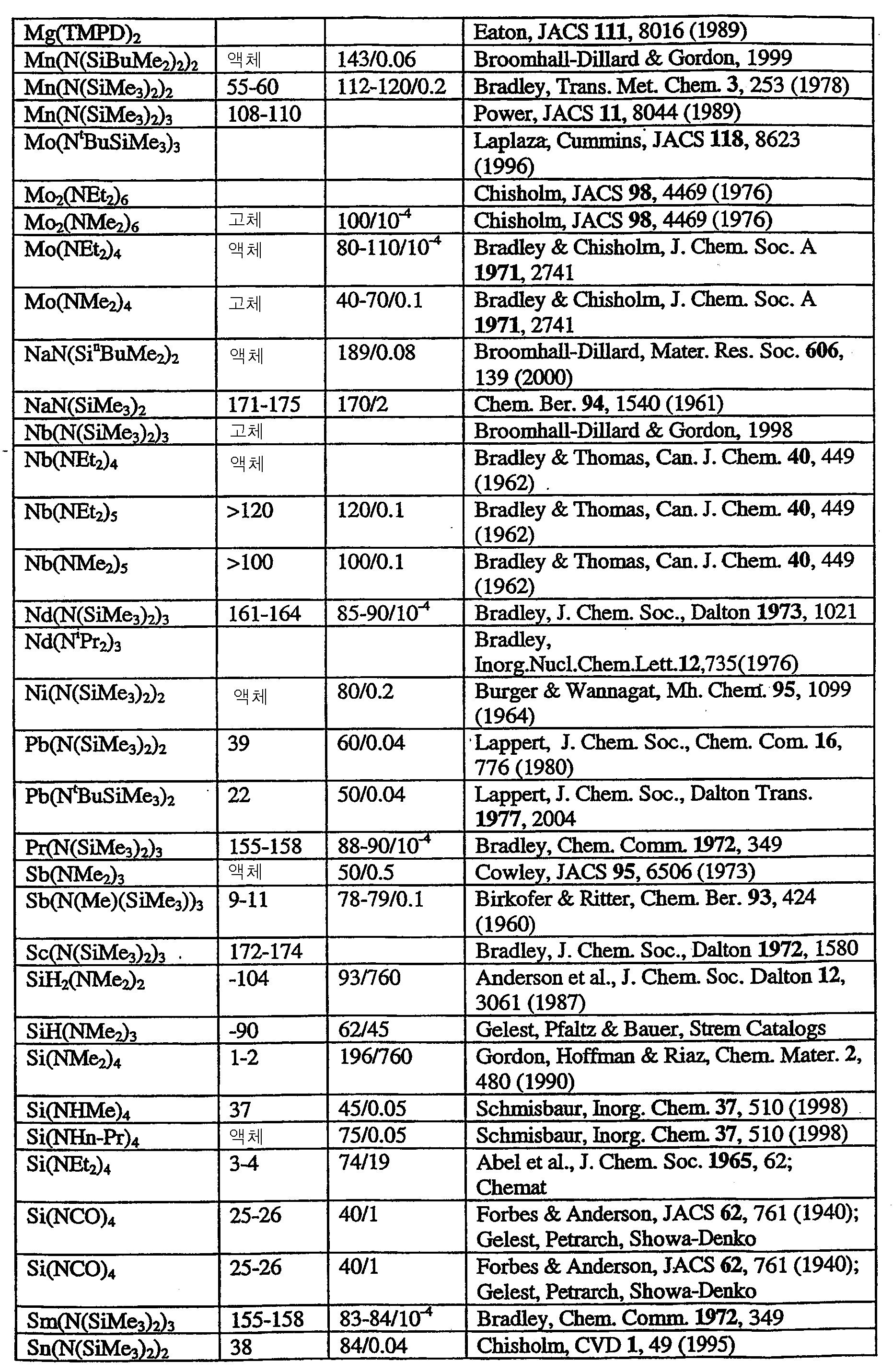
- 제 1항에 있어서, 상기 하나 이상의 금속 아마이드는 표 1로부터 선택된 것을 특징으로 하는 방법.
Applications Claiming Priority (4)
| Application Number | Priority Date | Filing Date | Title |
|---|---|---|---|
| US23628300P | 2000-09-28 | 2000-09-28 | |
| US60/236,283 | 2000-09-28 | ||
| US25391700P | 2000-11-29 | 2000-11-29 | |
| US60/253,917 | 2000-11-29 |
Related Parent Applications (1)
| Application Number | Title | Priority Date | Filing Date |
|---|---|---|---|
| KR1020037004494A Division KR100815009B1 (ko) | 2000-09-28 | 2001-09-28 | 산화물, 규산염 및 인산염의 증기를 이용한 석출 |
Publications (2)
| Publication Number | Publication Date |
|---|---|
| KR20070107813A KR20070107813A (ko) | 2007-11-07 |
| KR100814980B1 true KR100814980B1 (ko) | 2008-03-18 |
Family
ID=26929629
Family Applications (2)
| Application Number | Title | Priority Date | Filing Date |
|---|---|---|---|
| KR1020077024096A KR100814980B1 (ko) | 2000-09-28 | 2001-09-28 | 산화물, 규산염 및 인산염의 증기를 이용한 석출 |
| KR1020037004494A KR100815009B1 (ko) | 2000-09-28 | 2001-09-28 | 산화물, 규산염 및 인산염의 증기를 이용한 석출 |
Family Applications After (1)
| Application Number | Title | Priority Date | Filing Date |
|---|---|---|---|
| KR1020037004494A KR100815009B1 (ko) | 2000-09-28 | 2001-09-28 | 산화물, 규산염 및 인산염의 증기를 이용한 석출 |
Country Status (5)
| Country | Link |
|---|---|
| US (8) | US6969539B2 (ko) |
| EP (2) | EP1327010B1 (ko) |
| JP (2) | JP5290488B2 (ko) |
| KR (2) | KR100814980B1 (ko) |
| WO (1) | WO2002027063A2 (ko) |
Families Citing this family (487)
| Publication number | Priority date | Publication date | Assignee | Title |
|---|---|---|---|---|
| US7157385B2 (en) | 2003-09-05 | 2007-01-02 | Micron Technology, Inc. | Method of depositing a silicon dioxide-comprising layer in the fabrication of integrated circuitry |
| US6300219B1 (en) | 1999-08-30 | 2001-10-09 | Micron Technology, Inc. | Method of forming trench isolation regions |
| FI118804B (fi) * | 1999-12-03 | 2008-03-31 | Asm Int | Menetelmä oksidikalvojen kasvattamiseksi |
| FI117979B (fi) * | 2000-04-14 | 2007-05-15 | Asm Int | Menetelmä oksidiohutkalvojen valmistamiseksi |
| US6620723B1 (en) * | 2000-06-27 | 2003-09-16 | Applied Materials, Inc. | Formation of boride barrier layers using chemisorption techniques |
| KR100814980B1 (ko) | 2000-09-28 | 2008-03-18 | 프레지던트 앤드 펠로우즈 오브 하바드 칼리지 | 산화물, 규산염 및 인산염의 증기를 이용한 석출 |
| US20070014801A1 (en) * | 2001-01-24 | 2007-01-18 | Gish Kurt C | Methods of diagnosis of prostate cancer, compositions and methods of screening for modulators of prostate cancer |
| JP3915054B2 (ja) * | 2002-03-05 | 2007-05-16 | 株式会社トリケミカル研究所 | 膜形成材料、膜形成方法、及び素子 |
| US6730163B2 (en) | 2002-03-14 | 2004-05-04 | Micron Technology, Inc. | Aluminum-containing material and atomic layer deposition methods |
| CN100360710C (zh) | 2002-03-28 | 2008-01-09 | 哈佛学院院长等 | 二氧化硅纳米层压材料的气相沉积 |
| KR100468847B1 (ko) * | 2002-04-02 | 2005-01-29 | 삼성전자주식회사 | 알콜을 이용한 금속산화물 박막의 화학기상증착법 |
| US7439191B2 (en) * | 2002-04-05 | 2008-10-21 | Applied Materials, Inc. | Deposition of silicon layers for active matrix liquid crystal display (AMLCD) applications |
| US6846516B2 (en) * | 2002-04-08 | 2005-01-25 | Applied Materials, Inc. | Multiple precursor cyclical deposition system |
| US20030235961A1 (en) * | 2002-04-17 | 2003-12-25 | Applied Materials, Inc. | Cyclical sequential deposition of multicomponent films |
| JP3627106B2 (ja) * | 2002-05-27 | 2005-03-09 | 株式会社高純度化学研究所 | 原子層吸着堆積法によるハフニウムシリケート薄膜の製造方法 |
| US7067439B2 (en) * | 2002-06-14 | 2006-06-27 | Applied Materials, Inc. | ALD metal oxide deposition process using direct oxidation |
| US6858547B2 (en) | 2002-06-14 | 2005-02-22 | Applied Materials, Inc. | System and method for forming a gate dielectric |
| US20030232501A1 (en) * | 2002-06-14 | 2003-12-18 | Kher Shreyas S. | Surface pre-treatment for enhancement of nucleation of high dielectric constant materials |
| CN1675402A (zh) * | 2002-07-12 | 2005-09-28 | 哈佛学院院长等 | 氮化钨的汽相沉积 |
| US20040014327A1 (en) * | 2002-07-18 | 2004-01-22 | Bing Ji | Method for etching high dielectric constant materials and for cleaning deposition chambers for high dielectric constant materials |
| US6960538B2 (en) * | 2002-08-21 | 2005-11-01 | Micron Technology, Inc. | Composite dielectric forming methods and composite dielectrics |
| US6958300B2 (en) * | 2002-08-28 | 2005-10-25 | Micron Technology, Inc. | Systems and methods for forming metal oxides using metal organo-amines and metal organo-oxides |
| US7112485B2 (en) * | 2002-08-28 | 2006-09-26 | Micron Technology, Inc. | Systems and methods for forming zirconium and/or hafnium-containing layers |
| US7041609B2 (en) * | 2002-08-28 | 2006-05-09 | Micron Technology, Inc. | Systems and methods for forming metal oxides using alcohols |
| US7033560B2 (en) | 2002-08-30 | 2006-04-25 | Air Products And Chemicals, Inc. | Single source mixtures of metal siloxides |
| US6936086B2 (en) * | 2002-09-11 | 2005-08-30 | Planar Systems, Inc. | High conductivity particle filter |
| KR100473806B1 (ko) * | 2002-09-28 | 2005-03-10 | 한국전자통신연구원 | 유기물 박막 및 유기물 소자를 위한 대면적 유기물 기상증착 장치 및 제조 방법 |
| DE10248980B4 (de) * | 2002-10-21 | 2004-11-11 | Infineon Technologies Ag | Verfahren zur Herstellung strukturierter Schichten aus Siliziumdioxid auf senkrecht oder geneigt zu einer Substratoberfläche angeordneten Prozessflächen |
| JP4009550B2 (ja) * | 2003-03-27 | 2007-11-14 | エルピーダメモリ株式会社 | 金属酸化膜の形成方法 |
| US20040198069A1 (en) * | 2003-04-04 | 2004-10-07 | Applied Materials, Inc. | Method for hafnium nitride deposition |
| JP4954448B2 (ja) * | 2003-04-05 | 2012-06-13 | ローム・アンド・ハース・エレクトロニック・マテリアルズ,エル.エル.シー. | 有機金属化合物 |
| TW200506093A (en) * | 2003-04-21 | 2005-02-16 | Aviza Tech Inc | System and method for forming multi-component films |
| US7141500B2 (en) * | 2003-06-05 | 2006-11-28 | American Air Liquide, Inc. | Methods for forming aluminum containing films utilizing amino aluminum precursors |
| US6835664B1 (en) | 2003-06-26 | 2004-12-28 | Micron Technology, Inc. | Methods of forming trenched isolation regions |
| US7125815B2 (en) | 2003-07-07 | 2006-10-24 | Micron Technology, Inc. | Methods of forming a phosphorous doped silicon dioxide comprising layer |
| JP4312006B2 (ja) * | 2003-08-25 | 2009-08-12 | 株式会社Adeka | 希土類金属錯体、薄膜形成用原料及び薄膜の製造方法 |
| US20050056219A1 (en) * | 2003-09-16 | 2005-03-17 | Tokyo Electron Limited | Formation of a metal-containing film by sequential gas exposure in a batch type processing system |
| US7312163B2 (en) | 2003-09-24 | 2007-12-25 | Micron Technology, Inc. | Atomic layer deposition methods, and methods of forming materials over semiconductor substrates |
| US6867152B1 (en) | 2003-09-26 | 2005-03-15 | Novellus Systems, Inc. | Properties of a silica thin film produced by a rapid vapor deposition (RVD) process |
| US7166528B2 (en) | 2003-10-10 | 2007-01-23 | Applied Materials, Inc. | Methods of selective deposition of heavily doped epitaxial SiGe |
| US7618681B2 (en) | 2003-10-28 | 2009-11-17 | Asm International N.V. | Process for producing bismuth-containing oxide films |
| WO2009105668A1 (en) * | 2008-02-20 | 2009-08-27 | President And Fellows Of Harvard College | Bicyclic guanidines, metal complexes thereof and their use in vapor deposition |
| US7203001B2 (en) * | 2003-12-19 | 2007-04-10 | Nanoopto Corporation | Optical retarders and related devices and systems |
| KR100519800B1 (ko) * | 2004-01-13 | 2005-10-10 | 삼성전자주식회사 | 란타늄 산화막의 제조방법 및 이를 이용한 모스 전계효과트랜지스터 및 캐패시터의 제조방법 |
| US20050181128A1 (en) * | 2004-02-12 | 2005-08-18 | Nikolov Anguel N. | Films for optical use and methods of making such films |
| KR20050091488A (ko) * | 2004-03-12 | 2005-09-15 | 주식회사 유피케미칼 | 세라믹 또는 금속박막 증착용 전구체 화합물 및 그제조방법 |
| US7053010B2 (en) | 2004-03-22 | 2006-05-30 | Micron Technology, Inc. | Methods of depositing silicon dioxide comprising layers in the fabrication of integrated circuitry, methods of forming trench isolation, and methods of forming arrays of memory cells |
| DE102004015174A1 (de) * | 2004-03-27 | 2005-10-13 | Aixtron Ag | Verfahren zum Abscheiden von insbesondere Metalloxiden mittels nicht kontinuierlicher Precursorinjektion |
| US20050275944A1 (en) | 2004-06-11 | 2005-12-15 | Wang Jian J | Optical films and methods of making the same |
| US7670758B2 (en) * | 2004-04-15 | 2010-03-02 | Api Nanofabrication And Research Corporation | Optical films and methods of making the same |
| JP2005322668A (ja) * | 2004-05-06 | 2005-11-17 | Renesas Technology Corp | 成膜装置および成膜方法 |
| US20050252449A1 (en) | 2004-05-12 | 2005-11-17 | Nguyen Son T | Control of gas flow and delivery to suppress the formation of particles in an MOCVD/ALD system |
| US8323754B2 (en) * | 2004-05-21 | 2012-12-04 | Applied Materials, Inc. | Stabilization of high-k dielectric materials |
| US8119210B2 (en) | 2004-05-21 | 2012-02-21 | Applied Materials, Inc. | Formation of a silicon oxynitride layer on a high-k dielectric material |
| US20060153995A1 (en) * | 2004-05-21 | 2006-07-13 | Applied Materials, Inc. | Method for fabricating a dielectric stack |
| US20060019033A1 (en) * | 2004-05-21 | 2006-01-26 | Applied Materials, Inc. | Plasma treatment of hafnium-containing materials |
| US20060062917A1 (en) * | 2004-05-21 | 2006-03-23 | Shankar Muthukrishnan | Vapor deposition of hafnium silicate materials with tris(dimethylamino)silane |
| US7129189B1 (en) | 2004-06-22 | 2006-10-31 | Novellus Systems, Inc. | Aluminum phosphate incorporation in silica thin films produced by rapid surface catalyzed vapor deposition (RVD) |
| US7202185B1 (en) | 2004-06-22 | 2007-04-10 | Novellus Systems, Inc. | Silica thin films produced by rapid surface catalyzed vapor deposition (RVD) using a nucleation layer |
| US7297608B1 (en) | 2004-06-22 | 2007-11-20 | Novellus Systems, Inc. | Method for controlling properties of conformal silica nanolaminates formed by rapid vapor deposition |
| US7097878B1 (en) | 2004-06-22 | 2006-08-29 | Novellus Systems, Inc. | Mixed alkoxy precursors and methods of their use for rapid vapor deposition of SiO2 films |
| US20060038293A1 (en) * | 2004-08-23 | 2006-02-23 | Rueger Neal R | Inter-metal dielectric fill |
| US8158488B2 (en) * | 2004-08-31 | 2012-04-17 | Micron Technology, Inc. | Method of increasing deposition rate of silicon dioxide on a catalyst |
| US7235459B2 (en) | 2004-08-31 | 2007-06-26 | Micron Technology, Inc. | Methods of forming trench isolation in the fabrication of integrated circuitry, methods of fabricating memory circuitry, integrated circuitry and memory integrated circuitry |
| KR100652378B1 (ko) * | 2004-09-08 | 2006-12-01 | 삼성전자주식회사 | 안티몬 프리커서 및 이를 이용한 상변화 메모리 소자의 제조방법 |
| US7790633B1 (en) | 2004-10-26 | 2010-09-07 | Novellus Systems, Inc. | Sequential deposition/anneal film densification method |
| US7148155B1 (en) | 2004-10-26 | 2006-12-12 | Novellus Systems, Inc. | Sequential deposition/anneal film densification method |
| US7682940B2 (en) * | 2004-12-01 | 2010-03-23 | Applied Materials, Inc. | Use of Cl2 and/or HCl during silicon epitaxial film formation |
| US7312128B2 (en) * | 2004-12-01 | 2007-12-25 | Applied Materials, Inc. | Selective epitaxy process with alternating gas supply |
| US7560352B2 (en) * | 2004-12-01 | 2009-07-14 | Applied Materials, Inc. | Selective deposition |
| US7064227B1 (en) * | 2004-12-09 | 2006-06-20 | Air Products And Chemicals, Inc. | Precursors for silica or metal silicate films |
| JP2006169556A (ja) * | 2004-12-13 | 2006-06-29 | Horiba Ltd | 金属酸化物薄膜の成膜方法 |
| US7619816B2 (en) * | 2004-12-15 | 2009-11-17 | Api Nanofabrication And Research Corp. | Structures for polarization and beam control |
| US20060127830A1 (en) * | 2004-12-15 | 2006-06-15 | Xuegong Deng | Structures for polarization and beam control |
| US7294583B1 (en) | 2004-12-23 | 2007-11-13 | Novellus Systems, Inc. | Methods for the use of alkoxysilanol precursors for vapor deposition of SiO2 films |
| KR100640620B1 (ko) * | 2004-12-27 | 2006-11-02 | 삼성전자주식회사 | 트윈비트 셀 구조의 nor형 플래쉬 메모리 소자 및 그제조 방법 |
| KR100618879B1 (ko) * | 2004-12-27 | 2006-09-01 | 삼성전자주식회사 | 게르마늄 전구체, 이를 이용하여 형성된 gst 박막,상기 박막의 제조 방법 및 상변화 메모리 소자 |
| US7223707B1 (en) | 2004-12-30 | 2007-05-29 | Novellus Systems, Inc. | Dynamic rapid vapor deposition process for conformal silica laminates |
| US7271112B1 (en) | 2004-12-30 | 2007-09-18 | Novellus Systems, Inc. | Methods for forming high density, conformal, silica nanolaminate films via pulsed deposition layer in structures of confined geometry |
| EP1676934A1 (en) * | 2004-12-30 | 2006-07-05 | STMicroelectronics S.r.l. | Chemical vapor deposition chamber for depositing titanium silicon nitride films for forming phase change memories |
| US7482247B1 (en) | 2004-12-30 | 2009-01-27 | Novellus Systems, Inc. | Conformal nanolaminate dielectric deposition and etch bag gap fill process |
| US7235492B2 (en) * | 2005-01-31 | 2007-06-26 | Applied Materials, Inc. | Low temperature etchant for treatment of silicon-containing surfaces |
| US7064224B1 (en) * | 2005-02-04 | 2006-06-20 | Air Products And Chemicals, Inc. | Organometallic complexes and their use as precursors to deposit metal films |
| US7217634B2 (en) | 2005-02-17 | 2007-05-15 | Micron Technology, Inc. | Methods of forming integrated circuitry |
| US7135418B1 (en) * | 2005-03-09 | 2006-11-14 | Novellus Systems, Inc. | Optimal operation of conformal silica deposition reactors |
| US7109129B1 (en) | 2005-03-09 | 2006-09-19 | Novellus Systems, Inc. | Optimal operation of conformal silica deposition reactors |
| FR2883287A1 (fr) * | 2005-03-16 | 2006-09-22 | Air Liquide | Precurseurs organo-metalliques et leur procede de fabrication |
| JP2006261434A (ja) | 2005-03-17 | 2006-09-28 | L'air Liquide Sa Pour L'etude & L'exploitation Des Procede S Georges Claude | シリコン酸化膜の形成方法 |
| US20060211241A1 (en) * | 2005-03-21 | 2006-09-21 | Christine Govern | Protective layer for barrier coating for silicon-containing substrate and process for preparing same |
| US20060210800A1 (en) * | 2005-03-21 | 2006-09-21 | Irene Spitsberg | Environmental barrier layer for silcon-containing substrate and process for preparing same |
| US7485338B2 (en) * | 2005-03-31 | 2009-02-03 | Tokyo Electron Limited | Method for precursor delivery |
| US8012847B2 (en) | 2005-04-01 | 2011-09-06 | Micron Technology, Inc. | Methods of forming trench isolation in the fabrication of integrated circuitry and methods of fabricating integrated circuitry |
| US7514119B2 (en) * | 2005-04-29 | 2009-04-07 | Linde, Inc. | Method and apparatus for using solution based precursors for atomic layer deposition |
| US7354651B2 (en) * | 2005-06-13 | 2008-04-08 | General Electric Company | Bond coat for corrosion resistant EBC for silicon-containing substrate and processes for preparing same |
| US7442444B2 (en) * | 2005-06-13 | 2008-10-28 | General Electric Company | Bond coat for silicon-containing substrate for EBC and processes for preparing same |
| US20060280954A1 (en) * | 2005-06-13 | 2006-12-14 | Irene Spitsberg | Corrosion resistant sealant for outer EBL of silicon-containing substrate and processes for preparing same |
| US20060280955A1 (en) * | 2005-06-13 | 2006-12-14 | Irene Spitsberg | Corrosion resistant sealant for EBC of silicon-containing substrate and processes for preparing same |
| US20060286774A1 (en) * | 2005-06-21 | 2006-12-21 | Applied Materials. Inc. | Method for forming silicon-containing materials during a photoexcitation deposition process |
| US7648927B2 (en) | 2005-06-21 | 2010-01-19 | Applied Materials, Inc. | Method for forming silicon-containing materials during a photoexcitation deposition process |
| US7651955B2 (en) | 2005-06-21 | 2010-01-26 | Applied Materials, Inc. | Method for forming silicon-containing materials during a photoexcitation deposition process |
| US20070049043A1 (en) * | 2005-08-23 | 2007-03-01 | Applied Materials, Inc. | Nitrogen profile engineering in HI-K nitridation for device performance enhancement and reliability improvement |
| US7402534B2 (en) | 2005-08-26 | 2008-07-22 | Applied Materials, Inc. | Pretreatment processes within a batch ALD reactor |
| US7521356B2 (en) * | 2005-09-01 | 2009-04-21 | Micron Technology, Inc. | Atomic layer deposition systems and methods including silicon-containing tantalum precursor compounds |
| US20070054048A1 (en) * | 2005-09-07 | 2007-03-08 | Suvi Haukka | Extended deposition range by hot spots |
| US7495743B2 (en) * | 2005-09-30 | 2009-02-24 | International Business Machines Corporation | Immersion optical lithography system having protective optical coating |
| US7393779B2 (en) * | 2005-10-31 | 2008-07-01 | International Business Machines Corporation | Shrinking contact apertures through LPD oxide |
| US7589028B1 (en) | 2005-11-15 | 2009-09-15 | Novellus Systems, Inc. | Hydroxyl bond removal and film densification method for oxide films using microwave post treatment |
| GB2432363B (en) * | 2005-11-16 | 2010-06-23 | Epichem Ltd | Hafnocene and zirconocene precursors, and use thereof in atomic layer deposition |
| US20070139771A1 (en) * | 2005-12-15 | 2007-06-21 | Jian Wang | Optical retarders and methods of making the same |
| US20070165308A1 (en) * | 2005-12-15 | 2007-07-19 | Jian Wang | Optical retarders and methods of making the same |
| US7713584B2 (en) | 2005-12-22 | 2010-05-11 | Asm International N.V. | Process for producing oxide films |
| US7491653B1 (en) | 2005-12-23 | 2009-02-17 | Novellus Systems, Inc. | Metal-free catalysts for pulsed deposition layer process for conformal silica laminates |
| US7510939B2 (en) | 2006-01-31 | 2009-03-31 | International Business Machines Corporation | Microelectronic structure by selective deposition |
| CA2535064A1 (fr) * | 2006-02-01 | 2007-08-01 | Hydro Quebec | Materiau multi-couches, procede de fabrication et utilisation comme electrode |
| KR20080092983A (ko) | 2006-02-07 | 2008-10-16 | 프레지던트 앤드 펠로우즈 오브 하바드 칼리지 | 탄소나노튜브의 기상 기능화 |
| US7964514B2 (en) * | 2006-03-02 | 2011-06-21 | Applied Materials, Inc. | Multiple nitrogen plasma treatments for thin SiON dielectrics |
| KR20160027244A (ko) | 2006-03-10 | 2016-03-09 | 인티그리스, 인코포레이티드 | 티타네이트, 란타네이트 및 탄탈레이트 유전막의 원자층 증착 및 화학 증기 증착용 전구체 조성물 |
| US20070217008A1 (en) * | 2006-03-17 | 2007-09-20 | Wang Jian J | Polarizer films and methods of making the same |
| US7737035B1 (en) | 2006-03-31 | 2010-06-15 | Novellus Systems, Inc. | Dual seal deposition process chamber and process |
| US7674337B2 (en) * | 2006-04-07 | 2010-03-09 | Applied Materials, Inc. | Gas manifolds for use during epitaxial film formation |
| US7288463B1 (en) | 2006-04-28 | 2007-10-30 | Novellus Systems, Inc. | Pulsed deposition layer gap fill with expansion material |
| US7798096B2 (en) | 2006-05-05 | 2010-09-21 | Applied Materials, Inc. | Plasma, UV and ion/neutral assisted ALD or CVD in a batch tool |
| CA2659099A1 (en) | 2006-06-15 | 2007-12-21 | Mars, Incorporated | Use of cocoa flavanols and procyanidins to improve executive cognitive and cerebral blood flow |
| US7625820B1 (en) | 2006-06-21 | 2009-12-01 | Novellus Systems, Inc. | Method of selective coverage of high aspect ratio structures with a conformal film |
| US8318966B2 (en) | 2006-06-23 | 2012-11-27 | Praxair Technology, Inc. | Organometallic compounds |
| US7956168B2 (en) * | 2006-07-06 | 2011-06-07 | Praxair Technology, Inc. | Organometallic compounds having sterically hindered amides |
| US20080032064A1 (en) * | 2006-07-10 | 2008-02-07 | President And Fellows Of Harvard College | Selective sealing of porous dielectric materials |
| KR100780865B1 (ko) | 2006-07-19 | 2007-11-30 | 삼성전자주식회사 | 상변화막을 포함하는 반도체 소자의 형성 방법 |
| EP2049705A4 (en) * | 2006-07-20 | 2014-10-29 | Linde Inc | IMPROVED METHODS FOR DEPOSITION OF ATOMIC LAYERS |
| US7795160B2 (en) | 2006-07-21 | 2010-09-14 | Asm America Inc. | ALD of metal silicate films |
| JP5090451B2 (ja) * | 2006-07-31 | 2012-12-05 | アプライド マテリアルズ インコーポレイテッド | 炭素含有シリコンエピタキシャル層の形成方法 |
| CN101496150B (zh) * | 2006-07-31 | 2012-07-18 | 应用材料公司 | 控制外延层形成期间形态的方法 |
| US7737047B2 (en) * | 2006-08-25 | 2010-06-15 | Micron Technology, Inc. | Semiconductor constructions, and methods of forming dielectric materials |
| US7956207B2 (en) * | 2006-09-28 | 2011-06-07 | Praxair Technology, Inc. | Heteroleptic organometallic compounds |
| US20080081114A1 (en) * | 2006-10-03 | 2008-04-03 | Novellus Systems, Inc. | Apparatus and method for delivering uniform fluid flow in a chemical deposition system |
| US7776395B2 (en) * | 2006-11-14 | 2010-08-17 | Applied Materials, Inc. | Method of depositing catalyst assisted silicates of high-k materials |
| US7749574B2 (en) | 2006-11-14 | 2010-07-06 | Applied Materials, Inc. | Low temperature ALD SiO2 |
| KR100852234B1 (ko) * | 2006-11-17 | 2008-08-13 | 삼성전자주식회사 | 금속 산화막의 형성 방법, 이를 이용한 게이트 구조물의제조 방법 및 커패시터의 제조 방법 |
| US8394196B2 (en) * | 2006-12-12 | 2013-03-12 | Applied Materials, Inc. | Formation of in-situ phosphorus doped epitaxial layer containing silicon and carbon |
| US7960236B2 (en) * | 2006-12-12 | 2011-06-14 | Applied Materials, Inc. | Phosphorus containing Si epitaxial layers in N-type source/drain junctions |
| US7678422B2 (en) * | 2006-12-13 | 2010-03-16 | Air Products And Chemicals, Inc. | Cyclic chemical vapor deposition of metal-silicon containing films |
| JP4353379B2 (ja) * | 2006-12-19 | 2009-10-28 | 株式会社トリケミカル研究所 | 膜形成材料、膜形成方法、及び素子 |
| US7993457B1 (en) | 2007-01-23 | 2011-08-09 | Novellus Systems, Inc. | Deposition sub-chamber with variable flow |
| US20080217730A1 (en) * | 2007-03-07 | 2008-09-11 | Toshiharu Furukawa | Methods of forming gas dielectric and related structure |
| US8624050B2 (en) * | 2007-06-22 | 2014-01-07 | General Electric Company | Solution process for transparent conductive oxide coatings |
| US20090035946A1 (en) * | 2007-07-31 | 2009-02-05 | Asm International N.V. | In situ deposition of different metal-containing films using cyclopentadienyl metal precursors |
| WO2009039187A1 (en) | 2007-09-17 | 2009-03-26 | L'air Liquide - Societe Anonyme Pour L'etude Et L'exploitation Des Procedes Georges Claude | Tellurium precursors for gst film deposition |
| US20090087561A1 (en) * | 2007-09-28 | 2009-04-02 | Advanced Technology Materials, Inc. | Metal and metalloid silylamides, ketimates, tetraalkylguanidinates and dianionic guanidinates useful for cvd/ald of thin films |
| WO2009049020A2 (en) * | 2007-10-11 | 2009-04-16 | Valence Process Equipment, Inc. | Chemical vapor deposition reactor |
| WO2009059237A2 (en) * | 2007-10-31 | 2009-05-07 | Advanced Technology Materials, Inc. | Novel bismuth precursors for cvd/ald of thin films |
| US20090117274A1 (en) * | 2007-11-06 | 2009-05-07 | Ce Ma | Solution based lanthanum precursors for atomic layer deposition |
| US20090130414A1 (en) * | 2007-11-08 | 2009-05-21 | Air Products And Chemicals, Inc. | Preparation of A Metal-containing Film Via ALD or CVD Processes |
| US8501637B2 (en) * | 2007-12-21 | 2013-08-06 | Asm International N.V. | Silicon dioxide thin films by ALD |
| US8016945B2 (en) * | 2007-12-21 | 2011-09-13 | Applied Materials, Inc. | Hafnium oxide ALD process |
| USRE47325E1 (en) | 2007-12-28 | 2019-03-26 | Universitetet I Oslo | Formation of a lithium comprising structure on a substrate by ALD |
| US7892968B2 (en) * | 2008-01-21 | 2011-02-22 | International Business Machines Corporation | Via gouging methods and related semiconductor structure |
| WO2009108930A1 (en) | 2008-02-29 | 2009-09-03 | Albemarle Corporation | Processes for producing transition metal amido and imido compounds |
| US7816278B2 (en) * | 2008-03-28 | 2010-10-19 | Tokyo Electron Limited | In-situ hybrid deposition of high dielectric constant films using atomic layer deposition and chemical vapor deposition |
| US7659158B2 (en) | 2008-03-31 | 2010-02-09 | Applied Materials, Inc. | Atomic layer deposition processes for non-volatile memory devices |
| US8383525B2 (en) * | 2008-04-25 | 2013-02-26 | Asm America, Inc. | Plasma-enhanced deposition process for forming a metal oxide thin film and related structures |
| TWI467045B (zh) | 2008-05-23 | 2015-01-01 | Sigma Aldrich Co | 高介電常數電介質薄膜與使用鈰基前驅物製造高介電常數電介質薄膜之方法 |
| KR20110014160A (ko) | 2008-05-29 | 2011-02-10 | 레르 리키드 쏘시에떼 아노님 뿌르 레드 에렉스뿔라따시옹 데 프로세데 조르즈 클로드 | 필름 증착을 위한 텔루륨 전구체 |
| US8802194B2 (en) | 2008-05-29 | 2014-08-12 | L'Air Liquide, Société Anonyme pour l'Etude et l'Exploitation des Procédés Georges Claude | Tellurium precursors for film deposition |
| US8636845B2 (en) | 2008-06-25 | 2014-01-28 | L'Air Liquide, Société Anonyme pour l'Etude et l'Exploitation des Procédés Georges Claude | Metal heterocyclic compounds for deposition of thin films |
| JP5639055B2 (ja) | 2008-08-01 | 2014-12-10 | レール・リキード−ソシエテ・アノニム・プール・レテュード・エ・レクスプロワタシオン・デ・プロセデ・ジョルジュ・クロード | タンタル含有層を基板上に形成する方法 |
| US8236381B2 (en) | 2008-08-08 | 2012-08-07 | L'air Liquide Societe Anonyme Pour L'etude Et L'exploitation Des Procedes Georges Claude | Metal piperidinate and metal pyridinate precursors for thin film deposition |
| US8491967B2 (en) | 2008-09-08 | 2013-07-23 | Applied Materials, Inc. | In-situ chamber treatment and deposition process |
| US20100062149A1 (en) | 2008-09-08 | 2010-03-11 | Applied Materials, Inc. | Method for tuning a deposition rate during an atomic layer deposition process |
| EP2406267B1 (en) | 2009-03-10 | 2019-02-20 | L'Air Liquide Société Anonyme pour l'Etude et l'Exploitation des Procédés Georges Claude | Cyclic amino compounds for low-k silylation |
| US9394608B2 (en) | 2009-04-06 | 2016-07-19 | Asm America, Inc. | Semiconductor processing reactor and components thereof |
| FI20095630A0 (fi) | 2009-06-05 | 2009-06-05 | Beneq Oy | Suojapinnoitus, menetelmä alustan suojaamiseksi ja menetelmän käyttö |
| WO2011005653A1 (en) | 2009-07-06 | 2011-01-13 | Llinde Aktiengesellschaft | Solution based precursors |
| JP5507909B2 (ja) * | 2009-07-14 | 2014-05-28 | 東京エレクトロン株式会社 | 成膜方法 |
| US8802201B2 (en) | 2009-08-14 | 2014-08-12 | Asm America, Inc. | Systems and methods for thin-film deposition of metal oxides using excited nitrogen-oxygen species |
| JP2013503849A (ja) | 2009-09-02 | 2013-02-04 | レール・リキード−ソシエテ・アノニム・プール・レテュード・エ・レクスプロワタシオン・デ・プロセデ・ジョルジュ・クロード | ゲルマニウム含有フィルムの堆積のための二ハロゲン化ゲルマニウム(ii)先駆物質 |
| WO2011057114A2 (en) * | 2009-11-09 | 2011-05-12 | L'air Liquide, Societe Anonyme Pour L'etude Et L'exploitation Des Procedes Georges Claude | Methods of making and deposition methods using hafnium- or zirconium-containing compounds |
| FI20096262A0 (fi) | 2009-11-30 | 2009-11-30 | Beneq Oy | Menetelmä koristepinnoitteen muodostamiseksi jalokiveen, jalokiven koristepinnoite, ja sen käytöt |
| WO2011095849A1 (en) | 2010-02-03 | 2011-08-11 | L'air Liquide, Societe Anonyme Pour L'etude Et L'exploitation Des Procedes Georges Claude | Chalcogenide-containing precursors, methods of making, and methods of using the same for thin film deposition |
| JP2013530264A (ja) | 2010-04-30 | 2013-07-25 | バテル メモリアル インスティチュート | 表面の清掃を容易にする組成物 |
| US9373677B2 (en) | 2010-07-07 | 2016-06-21 | Entegris, Inc. | Doping of ZrO2 for DRAM applications |
| EP2444405A1 (en) | 2010-10-07 | 2012-04-25 | L'Air Liquide Société Anonyme pour l'Etude et l'Exploitation des Procédés Georges Claude | Metal compounds for deposition of chalcogenide films at low temperature |
| EP2444406A1 (en) | 2010-10-07 | 2012-04-25 | L'Air Liquide Société Anonyme pour l'Etude et l'Exploitation des Procédés Georges Claude | Metal compounds for deposition of chalcogenide films at low temperature |
| EP2444404A1 (en) | 2010-10-07 | 2012-04-25 | L'Air Liquide Société Anonyme pour l'Etude et l'Exploitation des Procédés Georges Claude | Metal compounds for deposition of chalcogenide films at low temperature |
| EP2444407A1 (en) | 2010-10-07 | 2012-04-25 | L'Air Liquide Société Anonyme pour l'Etude et l'Exploitation des Procédés Georges Claude | Metal compounds for deposition of chalcogenide films at low temperature |
| KR101274522B1 (ko) * | 2010-11-30 | 2013-06-13 | 한양대학교 산학협력단 | 탄소나노튜브 3차원 네트워크를 이용한 미세유체 필터 및 그 제조 방법 |
| FR2968677A1 (fr) * | 2010-12-09 | 2012-06-15 | Commissariat Energie Atomique | Procédé de fabrication de couches a base de lithium par cvd |
| US8946096B2 (en) * | 2011-03-15 | 2015-02-03 | Mecharonics Co. Ltd. | Group IV-B organometallic compound, and method for preparing same |
| US9315894B2 (en) | 2011-03-30 | 2016-04-19 | Asm Ip Holding B.V. | Atomic layer deposition of metal phosphates and lithium silicates |
| WO2013011297A1 (en) * | 2011-07-15 | 2013-01-24 | Universitetet I Oslo | Method |
| US20130023129A1 (en) | 2011-07-20 | 2013-01-24 | Asm America, Inc. | Pressure transmitter for a semiconductor processing environment |
| US20130022658A1 (en) * | 2011-07-23 | 2013-01-24 | Synos Technology, Inc. | Depositing material with antimicrobial properties on permeable substrate using atomic layer deposition |
| WO2013046157A1 (en) | 2011-09-27 | 2013-04-04 | L'air Liquide, Societe Anonyme Pour L'etude Et L'exploitation Des Procedes Georges Claude | Nickel bis diazabutadiene precursors, their synthesis, and their use for nickel containing film depositions |
| US9017481B1 (en) | 2011-10-28 | 2015-04-28 | Asm America, Inc. | Process feed management for semiconductor substrate processing |
| WO2013078110A1 (en) * | 2011-11-21 | 2013-05-30 | President And Fellows Of Harvard College | Self-aligned deposition of silica layers for dye-sensitized solar cells |
| US8901706B2 (en) | 2012-01-06 | 2014-12-02 | International Business Machines Corporation | Thermally stable high-K tetragonal HFO2 layer within high aspect ratio deep trenches |
| US9048294B2 (en) * | 2012-04-13 | 2015-06-02 | Applied Materials, Inc. | Methods for depositing manganese and manganese nitrides |
| WO2013177326A1 (en) | 2012-05-25 | 2013-11-28 | Advanced Technology Materials, Inc. | Silicon precursors for low temperature ald of silicon-based thin-films |
| US10714315B2 (en) | 2012-10-12 | 2020-07-14 | Asm Ip Holdings B.V. | Semiconductor reaction chamber showerhead |
| US20160376700A1 (en) | 2013-02-01 | 2016-12-29 | Asm Ip Holding B.V. | System for treatment of deposition reactor |
| US10186570B2 (en) | 2013-02-08 | 2019-01-22 | Entegris, Inc. | ALD processes for low leakage current and low equivalent oxide thickness BiTaO films |
| CN105027316B (zh) * | 2013-03-14 | 2018-07-17 | 应用材料公司 | 薄膜封装-用于oled应用的薄超高阻挡层 |
| US9353439B2 (en) | 2013-04-05 | 2016-05-31 | Lam Research Corporation | Cascade design showerhead for transient uniformity |
| JP2016525550A (ja) * | 2013-07-26 | 2016-08-25 | プレジデント アンド フェローズ オブ ハーバード カレッジ | 環状アミンの金属アミド |
| US10554624B2 (en) * | 2013-09-25 | 2020-02-04 | Mcafee, Llc | Proxy authentication for single sign-on |
| WO2015056944A1 (ko) * | 2013-10-14 | 2015-04-23 | 한국화학연구원 | 몰리브데넘 화합물 또는 텅스텐 화합물, 이의 제조 방법 및 이를 이용하여 박막을 형성하는 방법 |
| US9518075B2 (en) | 2013-12-13 | 2016-12-13 | L'Air Liquide, Société Anonyme pour l'Etude et l'Exploitation des Procédés Georges Claude | Group 5 cyclopentadienyl transition metal-containing precursors for deposition of group 5 transition metal-containing films |
| US11286557B2 (en) * | 2014-01-24 | 2022-03-29 | Commissariat A L'energie Atomique Et Aux Engergies Alternatives | Method of forming a crystalline thin film having the formula MY2 using an ALD-formed amorphous thin film having the formula MYx as a precursor |
| US11015245B2 (en) | 2014-03-19 | 2021-05-25 | Asm Ip Holding B.V. | Gas-phase reactor and system having exhaust plenum and components thereof |
| WO2015200758A2 (en) * | 2014-06-26 | 2015-12-30 | Tufts University | 3d graphene transistor |
| US10858737B2 (en) | 2014-07-28 | 2020-12-08 | Asm Ip Holding B.V. | Showerhead assembly and components thereof |
| US9890456B2 (en) | 2014-08-21 | 2018-02-13 | Asm Ip Holding B.V. | Method and system for in situ formation of gas-phase compounds |
| KR101590720B1 (ko) * | 2014-08-25 | 2016-02-03 | 고려대학교 산학협력단 | 원자층 증착 공정을 이용한 금속 인산화물 박막의 형성 방법 |
| US10941490B2 (en) | 2014-10-07 | 2021-03-09 | Asm Ip Holding B.V. | Multiple temperature range susceptor, assembly, reactor and system including the susceptor, and methods of using the same |
| JP5913663B2 (ja) * | 2015-02-19 | 2016-04-27 | 株式会社Adeka | モリブデンアミド化合物 |
| US10276355B2 (en) | 2015-03-12 | 2019-04-30 | Asm Ip Holding B.V. | Multi-zone reactor, system including the reactor, and method of using the same |
| US10763103B2 (en) * | 2015-03-31 | 2020-09-01 | Versum Materials Us, Llc | Boron-containing compounds, compositions, and methods for the deposition of a boron containing films |
| US10023959B2 (en) | 2015-05-26 | 2018-07-17 | Lam Research Corporation | Anti-transient showerhead |
| US10458018B2 (en) | 2015-06-26 | 2019-10-29 | Asm Ip Holding B.V. | Structures including metal carbide material, devices including the structures, and methods of forming same |
| DE102015217809A1 (de) * | 2015-09-17 | 2017-03-23 | Robert Bosch Gmbh | Vorlithiiertes, kohlenstoffbeschichtetes Anodenaktivmaterial |
| TWI740848B (zh) * | 2015-10-16 | 2021-10-01 | 荷蘭商Asm智慧財產控股公司 | 實施原子層沉積以得閘極介電質 |
| US10211308B2 (en) | 2015-10-21 | 2019-02-19 | Asm Ip Holding B.V. | NbMC layers |
| US10570514B2 (en) | 2015-11-30 | 2020-02-25 | Basf Se | Process for the generation of metallic films |
| TWI742022B (zh) * | 2015-11-30 | 2021-10-11 | 德商巴斯夫歐洲公司 | 生成金屬膜的方法 |
| US11139308B2 (en) | 2015-12-29 | 2021-10-05 | Asm Ip Holding B.V. | Atomic layer deposition of III-V compounds to form V-NAND devices |
| US9719167B2 (en) | 2015-12-31 | 2017-08-01 | L'Air Liquide, Société Anonyme pour l'Etude et l'Exploitation des Procédés Georges Claude | Cobalt-containing film forming compositions, their synthesis, and use in film deposition |
| GB201523156D0 (en) * | 2015-12-31 | 2016-02-17 | Pilkington Group Ltd | High strength glass containers |
| US9738971B2 (en) | 2015-12-31 | 2017-08-22 | L'Air Liquide, Société Anonyme pour l'Etude et l'Exploitation des Procédés Georges Claude | Vapor deposition methods to form group 8-containing films |
| US10011903B2 (en) | 2015-12-31 | 2018-07-03 | L'Air Liquide, Société Anonyme pour l'Etude et l'Exploitation des Procédés Georges Claude | Manganese-containing film forming compositions, their synthesis, and use in film deposition |
| US10529554B2 (en) | 2016-02-19 | 2020-01-07 | Asm Ip Holding B.V. | Method for forming silicon nitride film selectively on sidewalls or flat surfaces of trenches |
| US10190213B2 (en) | 2016-04-21 | 2019-01-29 | Asm Ip Holding B.V. | Deposition of metal borides |
| US10865475B2 (en) | 2016-04-21 | 2020-12-15 | Asm Ip Holding B.V. | Deposition of metal borides and silicides |
| US10651080B2 (en) | 2016-04-26 | 2020-05-12 | Lam Research Corporation | Oxidizing treatment of aluminum nitride films in semiconductor device manufacturing |
| US10367080B2 (en) | 2016-05-02 | 2019-07-30 | Asm Ip Holding B.V. | Method of forming a germanium oxynitride film |
| JP6548086B2 (ja) * | 2016-05-17 | 2019-07-24 | 株式会社フィルテック | 膜形成方法 |
| US11453943B2 (en) | 2016-05-25 | 2022-09-27 | Asm Ip Holding B.V. | Method for forming carbon-containing silicon/metal oxide or nitride film by ALD using silicon precursor and hydrocarbon precursor |
| US9859151B1 (en) | 2016-07-08 | 2018-01-02 | Asm Ip Holding B.V. | Selective film deposition method to form air gaps |
| US10612137B2 (en) | 2016-07-08 | 2020-04-07 | Asm Ip Holdings B.V. | Organic reactants for atomic layer deposition |
| US10714385B2 (en) | 2016-07-19 | 2020-07-14 | Asm Ip Holding B.V. | Selective deposition of tungsten |
| KR102532607B1 (ko) | 2016-07-28 | 2023-05-15 | 에이에스엠 아이피 홀딩 비.브이. | 기판 가공 장치 및 그 동작 방법 |
| US9812320B1 (en) | 2016-07-28 | 2017-11-07 | Asm Ip Holding B.V. | Method and apparatus for filling a gap |
| US9887082B1 (en) | 2016-07-28 | 2018-02-06 | Asm Ip Holding B.V. | Method and apparatus for filling a gap |
| US10049869B2 (en) * | 2016-09-30 | 2018-08-14 | Lam Research Corporation | Composite dielectric interface layers for interconnect structures |
| US10643826B2 (en) | 2016-10-26 | 2020-05-05 | Asm Ip Holdings B.V. | Methods for thermally calibrating reaction chambers |
| US11532757B2 (en) | 2016-10-27 | 2022-12-20 | Asm Ip Holding B.V. | Deposition of charge trapping layers |
| US10714350B2 (en) | 2016-11-01 | 2020-07-14 | ASM IP Holdings, B.V. | Methods for forming a transition metal niobium nitride film on a substrate by atomic layer deposition and related semiconductor device structures |
| US10229833B2 (en) | 2016-11-01 | 2019-03-12 | Asm Ip Holding B.V. | Methods for forming a transition metal nitride film on a substrate by atomic layer deposition and related semiconductor device structures |
| US9859153B1 (en) | 2016-11-14 | 2018-01-02 | Lam Research Corporation | Deposition of aluminum oxide etch stop layers |
| KR102546317B1 (ko) | 2016-11-15 | 2023-06-21 | 에이에스엠 아이피 홀딩 비.브이. | 기체 공급 유닛 및 이를 포함하는 기판 처리 장치 |
| KR20180068582A (ko) | 2016-12-14 | 2018-06-22 | 에이에스엠 아이피 홀딩 비.브이. | 기판 처리 장치 |
| US11447861B2 (en) | 2016-12-15 | 2022-09-20 | Asm Ip Holding B.V. | Sequential infiltration synthesis apparatus and a method of forming a patterned structure |
| US11581186B2 (en) | 2016-12-15 | 2023-02-14 | Asm Ip Holding B.V. | Sequential infiltration synthesis apparatus |
| KR20180070971A (ko) | 2016-12-19 | 2018-06-27 | 에이에스엠 아이피 홀딩 비.브이. | 기판 처리 장치 |
| US10269558B2 (en) | 2016-12-22 | 2019-04-23 | Asm Ip Holding B.V. | Method of forming a structure on a substrate |
| US10867788B2 (en) | 2016-12-28 | 2020-12-15 | Asm Ip Holding B.V. | Method of forming a structure on a substrate |
| US11390950B2 (en) | 2017-01-10 | 2022-07-19 | Asm Ip Holding B.V. | Reactor system and method to reduce residue buildup during a film deposition process |
| US10468261B2 (en) | 2017-02-15 | 2019-11-05 | Asm Ip Holding B.V. | Methods for forming a metallic film on a substrate by cyclical deposition and related semiconductor device structures |
| US10043656B1 (en) * | 2017-03-10 | 2018-08-07 | Lam Research Corporation | Selective growth of silicon oxide or silicon nitride on silicon surfaces in the presence of silicon oxide |
| CN110475901B (zh) * | 2017-03-15 | 2022-08-09 | 佳能奥普特龙株式会社 | 亲水性蒸镀膜以及蒸镀材料 |
| US10529563B2 (en) | 2017-03-29 | 2020-01-07 | Asm Ip Holdings B.V. | Method for forming doped metal oxide films on a substrate by cyclical deposition and related semiconductor device structures |
| KR102545882B1 (ko) | 2017-04-11 | 2023-06-20 | 도쿄엘렉트론가부시키가이샤 | 역행 프로파일들을 갖는 리세스된 피처들을 보이드 없이 충전하는 방법 |
| KR102457289B1 (ko) | 2017-04-25 | 2022-10-21 | 에이에스엠 아이피 홀딩 비.브이. | 박막 증착 방법 및 반도체 장치의 제조 방법 |
| EP3619323A4 (en) | 2017-05-05 | 2021-01-27 | Quantum-si Incorporated | SUBSTRATES WITH MODIFIED SURFACE REACTIVITY AND ANTIFOULING PROPERTIES IN BIOLOGICAL REACTIONS |
| US10892156B2 (en) | 2017-05-08 | 2021-01-12 | Asm Ip Holding B.V. | Methods for forming a silicon nitride film on a substrate and related semiconductor device structures |
| US10770286B2 (en) | 2017-05-08 | 2020-09-08 | Asm Ip Holdings B.V. | Methods for selectively forming a silicon nitride film on a substrate and related semiconductor device structures |
| US10886123B2 (en) | 2017-06-02 | 2021-01-05 | Asm Ip Holding B.V. | Methods for forming low temperature semiconductor layers and related semiconductor device structures |
| US11306395B2 (en) | 2017-06-28 | 2022-04-19 | Asm Ip Holding B.V. | Methods for depositing a transition metal nitride film on a substrate by atomic layer deposition and related deposition apparatus |
| US11114347B2 (en) | 2017-06-30 | 2021-09-07 | Taiwan Semiconductor Manufacturing Co., Ltd. | Self-protective layer formed on high-k dielectric layers with different materials |
| US10283417B1 (en) * | 2017-06-30 | 2019-05-07 | Taiwan Semiconductor Manufacturing Co., Ltd. | Self-protective layer formed on high-k dielectric layers with different materials |
| US10685834B2 (en) | 2017-07-05 | 2020-06-16 | Asm Ip Holdings B.V. | Methods for forming a silicon germanium tin layer and related semiconductor device structures |
| KR20190009245A (ko) | 2017-07-18 | 2019-01-28 | 에이에스엠 아이피 홀딩 비.브이. | 반도체 소자 구조물 형성 방법 및 관련된 반도체 소자 구조물 |
| US10541333B2 (en) | 2017-07-19 | 2020-01-21 | Asm Ip Holding B.V. | Method for depositing a group IV semiconductor and related semiconductor device structures |
| US11374112B2 (en) | 2017-07-19 | 2022-06-28 | Asm Ip Holding B.V. | Method for depositing a group IV semiconductor and related semiconductor device structures |
| US11018002B2 (en) | 2017-07-19 | 2021-05-25 | Asm Ip Holding B.V. | Method for selectively depositing a Group IV semiconductor and related semiconductor device structures |
| US10590535B2 (en) | 2017-07-26 | 2020-03-17 | Asm Ip Holdings B.V. | Chemical treatment, deposition and/or infiltration apparatus and method for using the same |
| US10692741B2 (en) | 2017-08-08 | 2020-06-23 | Asm Ip Holdings B.V. | Radiation shield |
| US10770336B2 (en) | 2017-08-08 | 2020-09-08 | Asm Ip Holding B.V. | Substrate lift mechanism and reactor including same |
| US11769682B2 (en) | 2017-08-09 | 2023-09-26 | Asm Ip Holding B.V. | Storage apparatus for storing cassettes for substrates and processing apparatus equipped therewith |
| US11139191B2 (en) | 2017-08-09 | 2021-10-05 | Asm Ip Holding B.V. | Storage apparatus for storing cassettes for substrates and processing apparatus equipped therewith |
| US11830730B2 (en) | 2017-08-29 | 2023-11-28 | Asm Ip Holding B.V. | Layer forming method and apparatus |
| US11056344B2 (en) | 2017-08-30 | 2021-07-06 | Asm Ip Holding B.V. | Layer forming method |
| US11295980B2 (en) | 2017-08-30 | 2022-04-05 | Asm Ip Holding B.V. | Methods for depositing a molybdenum metal film over a dielectric surface of a substrate by a cyclical deposition process and related semiconductor device structures |
| KR102491945B1 (ko) | 2017-08-30 | 2023-01-26 | 에이에스엠 아이피 홀딩 비.브이. | 기판 처리 장치 |
| KR102401446B1 (ko) | 2017-08-31 | 2022-05-24 | 에이에스엠 아이피 홀딩 비.브이. | 기판 처리 장치 |
| KR102630301B1 (ko) | 2017-09-21 | 2024-01-29 | 에이에스엠 아이피 홀딩 비.브이. | 침투성 재료의 순차 침투 합성 방법 처리 및 이를 이용하여 형성된 구조물 및 장치 |
| US10844484B2 (en) | 2017-09-22 | 2020-11-24 | Asm Ip Holding B.V. | Apparatus for dispensing a vapor phase reactant to a reaction chamber and related methods |
| US10658205B2 (en) | 2017-09-28 | 2020-05-19 | Asm Ip Holdings B.V. | Chemical dispensing apparatus and methods for dispensing a chemical to a reaction chamber |
| US10403504B2 (en) | 2017-10-05 | 2019-09-03 | Asm Ip Holding B.V. | Method for selectively depositing a metallic film on a substrate |
| US10319588B2 (en) | 2017-10-10 | 2019-06-11 | Asm Ip Holding B.V. | Method for depositing a metal chalcogenide on a substrate by cyclical deposition |
| US10923344B2 (en) | 2017-10-30 | 2021-02-16 | Asm Ip Holding B.V. | Methods for forming a semiconductor structure and related semiconductor structures |
| US10910262B2 (en) | 2017-11-16 | 2021-02-02 | Asm Ip Holding B.V. | Method of selectively depositing a capping layer structure on a semiconductor device structure |
| US11022879B2 (en) | 2017-11-24 | 2021-06-01 | Asm Ip Holding B.V. | Method of forming an enhanced unexposed photoresist layer |
| WO2019103613A1 (en) | 2017-11-27 | 2019-05-31 | Asm Ip Holding B.V. | A storage device for storing wafer cassettes for use with a batch furnace |
| KR102633318B1 (ko) | 2017-11-27 | 2024-02-05 | 에이에스엠 아이피 홀딩 비.브이. | 청정 소형 구역을 포함한 장치 |
| US10872771B2 (en) | 2018-01-16 | 2020-12-22 | Asm Ip Holding B. V. | Method for depositing a material film on a substrate within a reaction chamber by a cyclical deposition process and related device structures |
| US11482412B2 (en) | 2018-01-19 | 2022-10-25 | Asm Ip Holding B.V. | Method for depositing a gap-fill layer by plasma-assisted deposition |
| TW202325889A (zh) | 2018-01-19 | 2023-07-01 | 荷蘭商Asm 智慧財產控股公司 | 沈積方法 |
| US11018047B2 (en) | 2018-01-25 | 2021-05-25 | Asm Ip Holding B.V. | Hybrid lift pin |
| USD880437S1 (en) | 2018-02-01 | 2020-04-07 | Asm Ip Holding B.V. | Gas supply plate for semiconductor manufacturing apparatus |
| US11081345B2 (en) | 2018-02-06 | 2021-08-03 | Asm Ip Holding B.V. | Method of post-deposition treatment for silicon oxide film |
| US10896820B2 (en) | 2018-02-14 | 2021-01-19 | Asm Ip Holding B.V. | Method for depositing a ruthenium-containing film on a substrate by a cyclical deposition process |
| EP3737779A1 (en) | 2018-02-14 | 2020-11-18 | ASM IP Holding B.V. | A method for depositing a ruthenium-containing film on a substrate by a cyclical deposition process |
| US10731249B2 (en) | 2018-02-15 | 2020-08-04 | Asm Ip Holding B.V. | Method of forming a transition metal containing film on a substrate by a cyclical deposition process, a method for supplying a transition metal halide compound to a reaction chamber, and related vapor deposition apparatus |
| KR102636427B1 (ko) | 2018-02-20 | 2024-02-13 | 에이에스엠 아이피 홀딩 비.브이. | 기판 처리 방법 및 장치 |
| US10975470B2 (en) | 2018-02-23 | 2021-04-13 | Asm Ip Holding B.V. | Apparatus for detecting or monitoring for a chemical precursor in a high temperature environment |
| US11473195B2 (en) | 2018-03-01 | 2022-10-18 | Asm Ip Holding B.V. | Semiconductor processing apparatus and a method for processing a substrate |
| US11629406B2 (en) | 2018-03-09 | 2023-04-18 | Asm Ip Holding B.V. | Semiconductor processing apparatus comprising one or more pyrometers for measuring a temperature of a substrate during transfer of the substrate |
| US11114283B2 (en) | 2018-03-16 | 2021-09-07 | Asm Ip Holding B.V. | Reactor, system including the reactor, and methods of manufacturing and using same |
| KR102646467B1 (ko) | 2018-03-27 | 2024-03-11 | 에이에스엠 아이피 홀딩 비.브이. | 기판 상에 전극을 형성하는 방법 및 전극을 포함하는 반도체 소자 구조 |
| US11230766B2 (en) | 2018-03-29 | 2022-01-25 | Asm Ip Holding B.V. | Substrate processing apparatus and method |
| US11088002B2 (en) | 2018-03-29 | 2021-08-10 | Asm Ip Holding B.V. | Substrate rack and a substrate processing system and method |
| KR102501472B1 (ko) | 2018-03-30 | 2023-02-20 | 에이에스엠 아이피 홀딩 비.브이. | 기판 처리 방법 |
| US10443126B1 (en) * | 2018-04-06 | 2019-10-15 | Applied Materials, Inc. | Zone-controlled rare-earth oxide ALD and CVD coatings |
| TWI811348B (zh) | 2018-05-08 | 2023-08-11 | 荷蘭商Asm 智慧財產控股公司 | 藉由循環沉積製程於基板上沉積氧化物膜之方法及相關裝置結構 |
| TWI816783B (zh) | 2018-05-11 | 2023-10-01 | 荷蘭商Asm 智慧財產控股公司 | 用於基板上形成摻雜金屬碳化物薄膜之方法及相關半導體元件結構 |
| KR102596988B1 (ko) | 2018-05-28 | 2023-10-31 | 에이에스엠 아이피 홀딩 비.브이. | 기판 처리 방법 및 그에 의해 제조된 장치 |
| US11718913B2 (en) | 2018-06-04 | 2023-08-08 | Asm Ip Holding B.V. | Gas distribution system and reactor system including same |
| US11270899B2 (en) | 2018-06-04 | 2022-03-08 | Asm Ip Holding B.V. | Wafer handling chamber with moisture reduction |
| US11286562B2 (en) | 2018-06-08 | 2022-03-29 | Asm Ip Holding B.V. | Gas-phase chemical reactor and method of using same |
| US11401599B2 (en) | 2018-06-18 | 2022-08-02 | Applied Materials, Inc. | Erosion resistant metal silicate coatings |
| US10797133B2 (en) | 2018-06-21 | 2020-10-06 | Asm Ip Holding B.V. | Method for depositing a phosphorus doped silicon arsenide film and related semiconductor device structures |
| KR102568797B1 (ko) | 2018-06-21 | 2023-08-21 | 에이에스엠 아이피 홀딩 비.브이. | 기판 처리 시스템 |
| US11492703B2 (en) | 2018-06-27 | 2022-11-08 | Asm Ip Holding B.V. | Cyclic deposition methods for forming metal-containing material and films and structures including the metal-containing material |
| KR20210027265A (ko) | 2018-06-27 | 2021-03-10 | 에이에스엠 아이피 홀딩 비.브이. | 금속 함유 재료를 형성하기 위한 주기적 증착 방법 및 금속 함유 재료를 포함하는 막 및 구조체 |
| KR20200002519A (ko) | 2018-06-29 | 2020-01-08 | 에이에스엠 아이피 홀딩 비.브이. | 박막 증착 방법 및 반도체 장치의 제조 방법 |
| US10612136B2 (en) | 2018-06-29 | 2020-04-07 | ASM IP Holding, B.V. | Temperature-controlled flange and reactor system including same |
| US10388513B1 (en) | 2018-07-03 | 2019-08-20 | Asm Ip Holding B.V. | Method for depositing silicon-free carbon-containing film as gap-fill layer by pulse plasma-assisted deposition |
| US10755922B2 (en) | 2018-07-03 | 2020-08-25 | Asm Ip Holding B.V. | Method for depositing silicon-free carbon-containing film as gap-fill layer by pulse plasma-assisted deposition |
| US10767789B2 (en) | 2018-07-16 | 2020-09-08 | Asm Ip Holding B.V. | Diaphragm valves, valve components, and methods for forming valve components |
| WO2020027552A1 (en) * | 2018-07-30 | 2020-02-06 | Up Chemical Co., Ltd. | Aluminum compounds and methods of forming aluminum-containing film using the same |
| US11053591B2 (en) | 2018-08-06 | 2021-07-06 | Asm Ip Holding B.V. | Multi-port gas injection system and reactor system including same |
| US10883175B2 (en) | 2018-08-09 | 2021-01-05 | Asm Ip Holding B.V. | Vertical furnace for processing substrates and a liner for use therein |
| US10829852B2 (en) | 2018-08-16 | 2020-11-10 | Asm Ip Holding B.V. | Gas distribution device for a wafer processing apparatus |
| US11430674B2 (en) | 2018-08-22 | 2022-08-30 | Asm Ip Holding B.V. | Sensor array, apparatus for dispensing a vapor phase reactant to a reaction chamber and related methods |
| US11024523B2 (en) | 2018-09-11 | 2021-06-01 | Asm Ip Holding B.V. | Substrate processing apparatus and method |
| KR20200030162A (ko) | 2018-09-11 | 2020-03-20 | 에이에스엠 아이피 홀딩 비.브이. | 박막 증착 방법 |
| US11049751B2 (en) | 2018-09-14 | 2021-06-29 | Asm Ip Holding B.V. | Cassette supply system to store and handle cassettes and processing apparatus equipped therewith |
| CN110970344A (zh) | 2018-10-01 | 2020-04-07 | Asm Ip控股有限公司 | 衬底保持设备、包含所述设备的系统及其使用方法 |
| US11232963B2 (en) | 2018-10-03 | 2022-01-25 | Asm Ip Holding B.V. | Substrate processing apparatus and method |
| KR102592699B1 (ko) | 2018-10-08 | 2023-10-23 | 에이에스엠 아이피 홀딩 비.브이. | 기판 지지 유닛 및 이를 포함하는 박막 증착 장치와 기판 처리 장치 |
| US10847365B2 (en) | 2018-10-11 | 2020-11-24 | Asm Ip Holding B.V. | Method of forming conformal silicon carbide film by cyclic CVD |
| US10811256B2 (en) | 2018-10-16 | 2020-10-20 | Asm Ip Holding B.V. | Method for etching a carbon-containing feature |
| KR102546322B1 (ko) | 2018-10-19 | 2023-06-21 | 에이에스엠 아이피 홀딩 비.브이. | 기판 처리 장치 및 기판 처리 방법 |
| KR102605121B1 (ko) | 2018-10-19 | 2023-11-23 | 에이에스엠 아이피 홀딩 비.브이. | 기판 처리 장치 및 기판 처리 방법 |
| USD948463S1 (en) | 2018-10-24 | 2022-04-12 | Asm Ip Holding B.V. | Susceptor for semiconductor substrate supporting apparatus |
| US11087997B2 (en) | 2018-10-31 | 2021-08-10 | Asm Ip Holding B.V. | Substrate processing apparatus for processing substrates |
| KR20200051105A (ko) | 2018-11-02 | 2020-05-13 | 에이에스엠 아이피 홀딩 비.브이. | 기판 지지 유닛 및 이를 포함하는 기판 처리 장치 |
| US11572620B2 (en) | 2018-11-06 | 2023-02-07 | Asm Ip Holding B.V. | Methods for selectively depositing an amorphous silicon film on a substrate |
| US11031242B2 (en) | 2018-11-07 | 2021-06-08 | Asm Ip Holding B.V. | Methods for depositing a boron doped silicon germanium film |
| US10847366B2 (en) | 2018-11-16 | 2020-11-24 | Asm Ip Holding B.V. | Methods for depositing a transition metal chalcogenide film on a substrate by a cyclical deposition process |
| US10818758B2 (en) | 2018-11-16 | 2020-10-27 | Asm Ip Holding B.V. | Methods for forming a metal silicate film on a substrate in a reaction chamber and related semiconductor device structures |
| US11217444B2 (en) | 2018-11-30 | 2022-01-04 | Asm Ip Holding B.V. | Method for forming an ultraviolet radiation responsive metal oxide-containing film |
| KR102636428B1 (ko) | 2018-12-04 | 2024-02-13 | 에이에스엠 아이피 홀딩 비.브이. | 기판 처리 장치를 세정하는 방법 |
| US11158513B2 (en) | 2018-12-13 | 2021-10-26 | Asm Ip Holding B.V. | Methods for forming a rhenium-containing film on a substrate by a cyclical deposition process and related semiconductor device structures |
| TW202037745A (zh) | 2018-12-14 | 2020-10-16 | 荷蘭商Asm Ip私人控股有限公司 | 形成裝置結構之方法、其所形成之結構及施行其之系統 |
| TW202405220A (zh) | 2019-01-17 | 2024-02-01 | 荷蘭商Asm Ip 私人控股有限公司 | 藉由循環沈積製程於基板上形成含過渡金屬膜之方法 |
| KR20200091543A (ko) | 2019-01-22 | 2020-07-31 | 에이에스엠 아이피 홀딩 비.브이. | 기판 처리 장치 |
| CN111524788B (zh) | 2019-02-01 | 2023-11-24 | Asm Ip私人控股有限公司 | 氧化硅的拓扑选择性膜形成的方法 |
| CN111593319B (zh) | 2019-02-20 | 2023-05-30 | Asm Ip私人控股有限公司 | 用于填充在衬底表面内形成的凹部的循环沉积方法和设备 |
| TW202044325A (zh) | 2019-02-20 | 2020-12-01 | 荷蘭商Asm Ip私人控股有限公司 | 填充一基板之一表面內所形成的一凹槽的方法、根據其所形成之半導體結構、及半導體處理設備 |
| KR20200102357A (ko) | 2019-02-20 | 2020-08-31 | 에이에스엠 아이피 홀딩 비.브이. | 3-d nand 응용의 플러그 충진체 증착용 장치 및 방법 |
| KR102626263B1 (ko) | 2019-02-20 | 2024-01-16 | 에이에스엠 아이피 홀딩 비.브이. | 처리 단계를 포함하는 주기적 증착 방법 및 이를 위한 장치 |
| JP2020133004A (ja) | 2019-02-22 | 2020-08-31 | エーエスエム・アイピー・ホールディング・ベー・フェー | 基材を処理するための基材処理装置および方法 |
| KR20200108242A (ko) | 2019-03-08 | 2020-09-17 | 에이에스엠 아이피 홀딩 비.브이. | 실리콘 질화물 층을 선택적으로 증착하는 방법, 및 선택적으로 증착된 실리콘 질화물 층을 포함하는 구조체 |
| KR20200108248A (ko) | 2019-03-08 | 2020-09-17 | 에이에스엠 아이피 홀딩 비.브이. | SiOCN 층을 포함한 구조체 및 이의 형성 방법 |
| KR20200108243A (ko) | 2019-03-08 | 2020-09-17 | 에이에스엠 아이피 홀딩 비.브이. | SiOC 층을 포함한 구조체 및 이의 형성 방법 |
| KR20200116033A (ko) | 2019-03-28 | 2020-10-08 | 에이에스엠 아이피 홀딩 비.브이. | 도어 개방기 및 이를 구비한 기판 처리 장치 |
| KR20200116855A (ko) | 2019-04-01 | 2020-10-13 | 에이에스엠 아이피 홀딩 비.브이. | 반도체 소자를 제조하는 방법 |
| US11447864B2 (en) | 2019-04-19 | 2022-09-20 | Asm Ip Holding B.V. | Layer forming method and apparatus |
| KR20200125453A (ko) | 2019-04-24 | 2020-11-04 | 에이에스엠 아이피 홀딩 비.브이. | 기상 반응기 시스템 및 이를 사용하는 방법 |
| KR20200130121A (ko) | 2019-05-07 | 2020-11-18 | 에이에스엠 아이피 홀딩 비.브이. | 딥 튜브가 있는 화학물질 공급원 용기 |
| KR20200130118A (ko) | 2019-05-07 | 2020-11-18 | 에이에스엠 아이피 홀딩 비.브이. | 비정질 탄소 중합체 막을 개질하는 방법 |
| KR20200130652A (ko) | 2019-05-10 | 2020-11-19 | 에이에스엠 아이피 홀딩 비.브이. | 표면 상에 재료를 증착하는 방법 및 본 방법에 따라 형성된 구조 |
| JP2020188254A (ja) | 2019-05-16 | 2020-11-19 | エーエスエム アイピー ホールディング ビー.ブイ. | ウェハボートハンドリング装置、縦型バッチ炉および方法 |
| JP2020188255A (ja) | 2019-05-16 | 2020-11-19 | エーエスエム アイピー ホールディング ビー.ブイ. | ウェハボートハンドリング装置、縦型バッチ炉および方法 |
| USD947913S1 (en) | 2019-05-17 | 2022-04-05 | Asm Ip Holding B.V. | Susceptor shaft |
| USD975665S1 (en) | 2019-05-17 | 2023-01-17 | Asm Ip Holding B.V. | Susceptor shaft |
| USD935572S1 (en) | 2019-05-24 | 2021-11-09 | Asm Ip Holding B.V. | Gas channel plate |
| US11773488B2 (en) * | 2019-05-30 | 2023-10-03 | Uchicago Argonne, Llc | Methods for low-temperature p-CVD and thermal ALD of magnesium diboride |
| USD922229S1 (en) | 2019-06-05 | 2021-06-15 | Asm Ip Holding B.V. | Device for controlling a temperature of a gas supply unit |
| KR20200141002A (ko) | 2019-06-06 | 2020-12-17 | 에이에스엠 아이피 홀딩 비.브이. | 배기 가스 분석을 포함한 기상 반응기 시스템을 사용하는 방법 |
| KR20200143254A (ko) | 2019-06-11 | 2020-12-23 | 에이에스엠 아이피 홀딩 비.브이. | 개질 가스를 사용하여 전자 구조를 형성하는 방법, 상기 방법을 수행하기 위한 시스템, 및 상기 방법을 사용하여 형성되는 구조 |
| USD944946S1 (en) | 2019-06-14 | 2022-03-01 | Asm Ip Holding B.V. | Shower plate |
| USD931978S1 (en) | 2019-06-27 | 2021-09-28 | Asm Ip Holding B.V. | Showerhead vacuum transport |
| KR20210005515A (ko) | 2019-07-03 | 2021-01-14 | 에이에스엠 아이피 홀딩 비.브이. | 기판 처리 장치용 온도 제어 조립체 및 이를 사용하는 방법 |
| JP7499079B2 (ja) | 2019-07-09 | 2024-06-13 | エーエスエム・アイピー・ホールディング・ベー・フェー | 同軸導波管を用いたプラズマ装置、基板処理方法 |
| CN112216646A (zh) | 2019-07-10 | 2021-01-12 | Asm Ip私人控股有限公司 | 基板支撑组件及包括其的基板处理装置 |
| KR20210010307A (ko) | 2019-07-16 | 2021-01-27 | 에이에스엠 아이피 홀딩 비.브이. | 기판 처리 장치 |
| KR20210010820A (ko) | 2019-07-17 | 2021-01-28 | 에이에스엠 아이피 홀딩 비.브이. | 실리콘 게르마늄 구조를 형성하는 방법 |
| KR20210010816A (ko) | 2019-07-17 | 2021-01-28 | 에이에스엠 아이피 홀딩 비.브이. | 라디칼 보조 점화 플라즈마 시스템 및 방법 |
| US11643724B2 (en) | 2019-07-18 | 2023-05-09 | Asm Ip Holding B.V. | Method of forming structures using a neutral beam |
| CN112242296A (zh) | 2019-07-19 | 2021-01-19 | Asm Ip私人控股有限公司 | 形成拓扑受控的无定形碳聚合物膜的方法 |
| TW202113936A (zh) | 2019-07-29 | 2021-04-01 | 荷蘭商Asm Ip私人控股有限公司 | 用於利用n型摻雜物及/或替代摻雜物選擇性沉積以達成高摻雜物併入之方法 |
| CN112309899A (zh) | 2019-07-30 | 2021-02-02 | Asm Ip私人控股有限公司 | 基板处理设备 |
| CN112309900A (zh) | 2019-07-30 | 2021-02-02 | Asm Ip私人控股有限公司 | 基板处理设备 |
| US11587815B2 (en) | 2019-07-31 | 2023-02-21 | Asm Ip Holding B.V. | Vertical batch furnace assembly |
| US11227782B2 (en) | 2019-07-31 | 2022-01-18 | Asm Ip Holding B.V. | Vertical batch furnace assembly |
| US11587814B2 (en) | 2019-07-31 | 2023-02-21 | Asm Ip Holding B.V. | Vertical batch furnace assembly |
| CN112323048B (zh) | 2019-08-05 | 2024-02-09 | Asm Ip私人控股有限公司 | 用于化学源容器的液位传感器 |
| USD965044S1 (en) | 2019-08-19 | 2022-09-27 | Asm Ip Holding B.V. | Susceptor shaft |
| USD965524S1 (en) | 2019-08-19 | 2022-10-04 | Asm Ip Holding B.V. | Susceptor support |
| JP2021031769A (ja) | 2019-08-21 | 2021-03-01 | エーエスエム アイピー ホールディング ビー.ブイ. | 成膜原料混合ガス生成装置及び成膜装置 |
| USD949319S1 (en) | 2019-08-22 | 2022-04-19 | Asm Ip Holding B.V. | Exhaust duct |
| KR20210024423A (ko) | 2019-08-22 | 2021-03-05 | 에이에스엠 아이피 홀딩 비.브이. | 홀을 구비한 구조체를 형성하기 위한 방법 |
| USD979506S1 (en) | 2019-08-22 | 2023-02-28 | Asm Ip Holding B.V. | Insulator |
| USD930782S1 (en) | 2019-08-22 | 2021-09-14 | Asm Ip Holding B.V. | Gas distributor |
| USD940837S1 (en) | 2019-08-22 | 2022-01-11 | Asm Ip Holding B.V. | Electrode |
| US11286558B2 (en) | 2019-08-23 | 2022-03-29 | Asm Ip Holding B.V. | Methods for depositing a molybdenum nitride film on a surface of a substrate by a cyclical deposition process and related semiconductor device structures including a molybdenum nitride film |
| KR20210024420A (ko) | 2019-08-23 | 2021-03-05 | 에이에스엠 아이피 홀딩 비.브이. | 비스(디에틸아미노)실란을 사용하여 peald에 의해 개선된 품질을 갖는 실리콘 산화물 막을 증착하기 위한 방법 |
| KR20210029090A (ko) | 2019-09-04 | 2021-03-15 | 에이에스엠 아이피 홀딩 비.브이. | 희생 캡핑 층을 이용한 선택적 증착 방법 |
| KR20210029663A (ko) | 2019-09-05 | 2021-03-16 | 에이에스엠 아이피 홀딩 비.브이. | 기판 처리 장치 |
| US11562901B2 (en) | 2019-09-25 | 2023-01-24 | Asm Ip Holding B.V. | Substrate processing method |
| CN112593212B (zh) | 2019-10-02 | 2023-12-22 | Asm Ip私人控股有限公司 | 通过循环等离子体增强沉积工艺形成拓扑选择性氧化硅膜的方法 |
| CN112635282A (zh) | 2019-10-08 | 2021-04-09 | Asm Ip私人控股有限公司 | 具有连接板的基板处理装置、基板处理方法 |
| TW202120432A (zh) | 2019-10-08 | 2021-06-01 | 法商液態空氣喬治斯克勞帝方法研究開發股份有限公司 | 用於沉積含鋰層、島或簇的鋰前驅體 |
| KR20210042810A (ko) | 2019-10-08 | 2021-04-20 | 에이에스엠 아이피 홀딩 비.브이. | 활성 종을 이용하기 위한 가스 분배 어셈블리를 포함한 반응기 시스템 및 이를 사용하는 방법 |
| KR20210043460A (ko) | 2019-10-10 | 2021-04-21 | 에이에스엠 아이피 홀딩 비.브이. | 포토레지스트 하부층을 형성하기 위한 방법 및 이를 포함한 구조체 |
| KR20220079943A (ko) * | 2019-10-11 | 2022-06-14 | 퀀텀-에스아이 인코포레이티드 | 증기 상에서의 표면 개질 |
| US12009241B2 (en) | 2019-10-14 | 2024-06-11 | Asm Ip Holding B.V. | Vertical batch furnace assembly with detector to detect cassette |
| TWI834919B (zh) | 2019-10-16 | 2024-03-11 | 荷蘭商Asm Ip私人控股有限公司 | 氧化矽之拓撲選擇性膜形成之方法 |
| US11637014B2 (en) | 2019-10-17 | 2023-04-25 | Asm Ip Holding B.V. | Methods for selective deposition of doped semiconductor material |
| KR20210047808A (ko) | 2019-10-21 | 2021-04-30 | 에이에스엠 아이피 홀딩 비.브이. | 막을 선택적으로 에칭하기 위한 장치 및 방법 |
| KR20210050453A (ko) | 2019-10-25 | 2021-05-07 | 에이에스엠 아이피 홀딩 비.브이. | 기판 표면 상의 갭 피처를 충진하는 방법 및 이와 관련된 반도체 소자 구조 |
| US11646205B2 (en) | 2019-10-29 | 2023-05-09 | Asm Ip Holding B.V. | Methods of selectively forming n-type doped material on a surface, systems for selectively forming n-type doped material, and structures formed using same |
| KR20210054983A (ko) | 2019-11-05 | 2021-05-14 | 에이에스엠 아이피 홀딩 비.브이. | 도핑된 반도체 층을 갖는 구조체 및 이를 형성하기 위한 방법 및 시스템 |
| US11501968B2 (en) | 2019-11-15 | 2022-11-15 | Asm Ip Holding B.V. | Method for providing a semiconductor device with silicon filled gaps |
| CN110922897B (zh) * | 2019-11-18 | 2024-03-08 | 宁波日晟新材料有限公司 | 一种用于硅化合物的低雾值无损伤抛光液及其制备方法 |
| KR20210062561A (ko) | 2019-11-20 | 2021-05-31 | 에이에스엠 아이피 홀딩 비.브이. | 기판의 표면 상에 탄소 함유 물질을 증착하는 방법, 상기 방법을 사용하여 형성된 구조물, 및 상기 구조물을 형성하기 위한 시스템 |
| KR20210065848A (ko) | 2019-11-26 | 2021-06-04 | 에이에스엠 아이피 홀딩 비.브이. | 제1 유전체 표면과 제2 금속성 표면을 포함한 기판 상에 타겟 막을 선택적으로 형성하기 위한 방법 |
| CN112951697A (zh) | 2019-11-26 | 2021-06-11 | Asm Ip私人控股有限公司 | 基板处理设备 |
| CN112885693A (zh) | 2019-11-29 | 2021-06-01 | Asm Ip私人控股有限公司 | 基板处理设备 |
| CN112885692A (zh) | 2019-11-29 | 2021-06-01 | Asm Ip私人控股有限公司 | 基板处理设备 |
| JP2021090042A (ja) | 2019-12-02 | 2021-06-10 | エーエスエム アイピー ホールディング ビー.ブイ. | 基板処理装置、基板処理方法 |
| KR20210070898A (ko) | 2019-12-04 | 2021-06-15 | 에이에스엠 아이피 홀딩 비.브이. | 기판 처리 장치 |
| TW202125596A (zh) | 2019-12-17 | 2021-07-01 | 荷蘭商Asm Ip私人控股有限公司 | 形成氮化釩層之方法以及包括該氮化釩層之結構 |
| US11527403B2 (en) | 2019-12-19 | 2022-12-13 | Asm Ip Holding B.V. | Methods for filling a gap feature on a substrate surface and related semiconductor structures |
| TW202140135A (zh) | 2020-01-06 | 2021-11-01 | 荷蘭商Asm Ip私人控股有限公司 | 氣體供應總成以及閥板總成 |
| US11993847B2 (en) | 2020-01-08 | 2024-05-28 | Asm Ip Holding B.V. | Injector |
| US11551912B2 (en) | 2020-01-20 | 2023-01-10 | Asm Ip Holding B.V. | Method of forming thin film and method of modifying surface of thin film |
| TW202130846A (zh) | 2020-02-03 | 2021-08-16 | 荷蘭商Asm Ip私人控股有限公司 | 形成包括釩或銦層的結構之方法 |
| TW202146882A (zh) | 2020-02-04 | 2021-12-16 | 荷蘭商Asm Ip私人控股有限公司 | 驗證一物品之方法、用於驗證一物品之設備、及用於驗證一反應室之系統 |
| US11776846B2 (en) | 2020-02-07 | 2023-10-03 | Asm Ip Holding B.V. | Methods for depositing gap filling fluids and related systems and devices |
| TW202146715A (zh) | 2020-02-17 | 2021-12-16 | 荷蘭商Asm Ip私人控股有限公司 | 用於生長磷摻雜矽層之方法及其系統 |
| TW202203344A (zh) | 2020-02-28 | 2022-01-16 | 荷蘭商Asm Ip控股公司 | 專用於零件清潔的系統 |
| KR20210116240A (ko) | 2020-03-11 | 2021-09-27 | 에이에스엠 아이피 홀딩 비.브이. | 조절성 접합부를 갖는 기판 핸들링 장치 |
| US11876356B2 (en) | 2020-03-11 | 2024-01-16 | Asm Ip Holding B.V. | Lockout tagout assembly and system and method of using same |
| CN113394086A (zh) | 2020-03-12 | 2021-09-14 | Asm Ip私人控股有限公司 | 用于制造具有目标拓扑轮廓的层结构的方法 |
| KR20210124042A (ko) | 2020-04-02 | 2021-10-14 | 에이에스엠 아이피 홀딩 비.브이. | 박막 형성 방법 |
| TW202146689A (zh) | 2020-04-03 | 2021-12-16 | 荷蘭商Asm Ip控股公司 | 阻障層形成方法及半導體裝置的製造方法 |
| TW202145344A (zh) | 2020-04-08 | 2021-12-01 | 荷蘭商Asm Ip私人控股有限公司 | 用於選擇性蝕刻氧化矽膜之設備及方法 |
| US11821078B2 (en) | 2020-04-15 | 2023-11-21 | Asm Ip Holding B.V. | Method for forming precoat film and method for forming silicon-containing film |
| US11996289B2 (en) | 2020-04-16 | 2024-05-28 | Asm Ip Holding B.V. | Methods of forming structures including silicon germanium and silicon layers, devices formed using the methods, and systems for performing the methods |
| KR20210132600A (ko) | 2020-04-24 | 2021-11-04 | 에이에스엠 아이피 홀딩 비.브이. | 바나듐, 질소 및 추가 원소를 포함한 층을 증착하기 위한 방법 및 시스템 |
| KR20210132605A (ko) | 2020-04-24 | 2021-11-04 | 에이에스엠 아이피 홀딩 비.브이. | 냉각 가스 공급부를 포함한 수직형 배치 퍼니스 어셈블리 |
| US11898243B2 (en) | 2020-04-24 | 2024-02-13 | Asm Ip Holding B.V. | Method of forming vanadium nitride-containing layer |
| KR20210134226A (ko) | 2020-04-29 | 2021-11-09 | 에이에스엠 아이피 홀딩 비.브이. | 고체 소스 전구체 용기 |
| KR20210134869A (ko) | 2020-05-01 | 2021-11-11 | 에이에스엠 아이피 홀딩 비.브이. | Foup 핸들러를 이용한 foup의 빠른 교환 |
| KR20210141379A (ko) | 2020-05-13 | 2021-11-23 | 에이에스엠 아이피 홀딩 비.브이. | 반응기 시스템용 레이저 정렬 고정구 |
| TW202147383A (zh) | 2020-05-19 | 2021-12-16 | 荷蘭商Asm Ip私人控股有限公司 | 基材處理設備 |
| KR20210145078A (ko) | 2020-05-21 | 2021-12-01 | 에이에스엠 아이피 홀딩 비.브이. | 다수의 탄소 층을 포함한 구조체 및 이를 형성하고 사용하는 방법 |
| TW202200837A (zh) | 2020-05-22 | 2022-01-01 | 荷蘭商Asm Ip私人控股有限公司 | 用於在基材上形成薄膜之反應系統 |
| TW202201602A (zh) | 2020-05-29 | 2022-01-01 | 荷蘭商Asm Ip私人控股有限公司 | 基板處理方法 |
| US11404465B2 (en) * | 2020-06-15 | 2022-08-02 | Taiwan Semiconductor Manufacturing Company Limited | Epitaxial semiconductor liner for enhancing uniformity of a charged layer in a deep trench and methods of forming the same |
| TW202218133A (zh) | 2020-06-24 | 2022-05-01 | 荷蘭商Asm Ip私人控股有限公司 | 形成含矽層之方法 |
| TW202217953A (zh) | 2020-06-30 | 2022-05-01 | 荷蘭商Asm Ip私人控股有限公司 | 基板處理方法 |
| TW202202649A (zh) | 2020-07-08 | 2022-01-16 | 荷蘭商Asm Ip私人控股有限公司 | 基板處理方法 |
| TW202219628A (zh) | 2020-07-17 | 2022-05-16 | 荷蘭商Asm Ip私人控股有限公司 | 用於光微影之結構與方法 |
| TW202204662A (zh) | 2020-07-20 | 2022-02-01 | 荷蘭商Asm Ip私人控股有限公司 | 用於沉積鉬層之方法及系統 |
| US11274069B2 (en) | 2020-08-13 | 2022-03-15 | L'Air Liquide, Société Anonyme pour l'Etude et l'Exploitation des Procédés Georges Claude | Mono-substituted cyclopentadienes and metal cyclopentadienyl complexes and synthesis methods thereof |
| TW202212623A (zh) | 2020-08-26 | 2022-04-01 | 荷蘭商Asm Ip私人控股有限公司 | 形成金屬氧化矽層及金屬氮氧化矽層的方法、半導體結構、及系統 |
| USD990534S1 (en) | 2020-09-11 | 2023-06-27 | Asm Ip Holding B.V. | Weighted lift pin |
| USD1012873S1 (en) | 2020-09-24 | 2024-01-30 | Asm Ip Holding B.V. | Electrode for semiconductor processing apparatus |
| US12009224B2 (en) | 2020-09-29 | 2024-06-11 | Asm Ip Holding B.V. | Apparatus and method for etching metal nitrides |
| TW202229613A (zh) | 2020-10-14 | 2022-08-01 | 荷蘭商Asm Ip私人控股有限公司 | 於階梯式結構上沉積材料的方法 |
| KR20220053482A (ko) | 2020-10-22 | 2022-04-29 | 에이에스엠 아이피 홀딩 비.브이. | 바나듐 금속을 증착하는 방법, 구조체, 소자 및 증착 어셈블리 |
| TW202223136A (zh) | 2020-10-28 | 2022-06-16 | 荷蘭商Asm Ip私人控股有限公司 | 用於在基板上形成層之方法、及半導體處理系統 |
| KR20220076343A (ko) | 2020-11-30 | 2022-06-08 | 에이에스엠 아이피 홀딩 비.브이. | 기판 처리 장치의 반응 챔버 내에 배열되도록 구성된 인젝터 |
| CN114639631A (zh) | 2020-12-16 | 2022-06-17 | Asm Ip私人控股有限公司 | 跳动和摆动测量固定装置 |
| TW202231903A (zh) | 2020-12-22 | 2022-08-16 | 荷蘭商Asm Ip私人控股有限公司 | 過渡金屬沉積方法、過渡金屬層、用於沉積過渡金屬於基板上的沉積總成 |
| US20220238323A1 (en) * | 2021-01-28 | 2022-07-28 | Tokyo Electron Limited | Method for selective deposition of dielectric on dielectric |
| KR20230154238A (ko) * | 2021-03-08 | 2023-11-07 | 가부시키가이샤 크리에이티브 코팅즈 | 제올라이트막의 제조 방법, 가스 흡착제 및 가스 흡착 장치 |
| KR20230157481A (ko) * | 2021-03-31 | 2023-11-16 | 도쿄엘렉트론가부시키가이샤 | 막 형성 방법 및 기판 처리 장치 |
| USD981973S1 (en) | 2021-05-11 | 2023-03-28 | Asm Ip Holding B.V. | Reactor wall for substrate processing apparatus |
| USD980813S1 (en) | 2021-05-11 | 2023-03-14 | Asm Ip Holding B.V. | Gas flow control plate for substrate processing apparatus |
| USD1023959S1 (en) | 2021-05-11 | 2024-04-23 | Asm Ip Holding B.V. | Electrode for substrate processing apparatus |
| USD980814S1 (en) | 2021-05-11 | 2023-03-14 | Asm Ip Holding B.V. | Gas distributor for substrate processing apparatus |
| KR102592398B1 (ko) * | 2021-05-12 | 2023-10-25 | 한국화학연구원 | 복합형광구조체 및 이의 제조방법 |
| USD990441S1 (en) | 2021-09-07 | 2023-06-27 | Asm Ip Holding B.V. | Gas flow control plate |
Citations (3)
| Publication number | Priority date | Publication date | Assignee | Title |
|---|---|---|---|---|
| US4792463A (en) * | 1985-09-17 | 1988-12-20 | Masaru Okada | Method of producing ferroelectric thin film |
| EP0560617A2 (en) * | 1992-03-13 | 1993-09-15 | Kawasaki Steel Corporation | Method of manufacturing insulating film on semiconductor device and apparatus for carrying out the same |
| WO1997038355A1 (en) * | 1996-04-08 | 1997-10-16 | Micrion Corporation | Systems and methods for deposition of dielectric films |
Family Cites Families (165)
| Publication number | Priority date | Publication date | Assignee | Title |
|---|---|---|---|---|
| FI117944B (fi) | 1999-10-15 | 2007-04-30 | Asm Int | Menetelmä siirtymämetallinitridiohutkalvojen kasvattamiseksi |
| SE393967B (sv) | 1974-11-29 | 1977-05-31 | Sateko Oy | Forfarande och for utforande av stroleggning mellan lagren i ett virkespaket |
| CA1087041A (en) | 1975-09-15 | 1980-10-07 | Mohammad J. Hakim | Hafnium carbide and nitride coatings |
| US4042610A (en) | 1975-09-22 | 1977-08-16 | E. I. Du Pont De Nemours And Company | Process for preparing hydrocarbyl and silahydrocarbyl transition metal dihydrocarbylamides |
| CA1093395A (en) | 1977-01-13 | 1981-01-13 | Mohammad J. Hakim | Chemical vapor deposition |
| FR2511047A1 (fr) | 1981-08-07 | 1983-02-11 | Solarex Corp | Procede pour appliquer un revetement antireflechissant et/ou dielectrique pour des cellules solaires |
| US4386117A (en) * | 1981-11-20 | 1983-05-31 | Gordon Roy G | Coating process using alkoxy substituted silicon-bearing reactant |
| JPS5916978A (ja) * | 1982-07-20 | 1984-01-28 | Tokyo Denshi Kagaku Kabushiki | 金属被膜の選択的エツチング方法 |
| US4512862A (en) | 1983-08-08 | 1985-04-23 | International Business Machines Corporation | Method of making a thin film insulator |
| EP0174743A3 (en) | 1984-09-05 | 1988-06-08 | Morton Thiokol, Inc. | Process for transition metal nitrides thin film deposition |
| US4723978A (en) * | 1985-10-31 | 1988-02-09 | International Business Machines Corporation | Method for a plasma-treated polysiloxane coating |
| US4758539A (en) | 1987-02-25 | 1988-07-19 | The United States Of America As Represented By The United States Department Of Energy | Process for producing ceramic nitrides and carbonitrides and their precursors |
| JPH0660406B2 (ja) | 1987-03-24 | 1994-08-10 | 日本電気株式会社 | ハフニウム酸化膜の気相成長法 |
| US4956323A (en) * | 1987-11-30 | 1990-09-11 | The Dow Chemical Company | Catalysts prepared from tetrakis(dialkylamide or diarylamide) derivatives of titanium and polymerization of olefins therewith |
| US4864374A (en) * | 1987-11-30 | 1989-09-05 | Texas Instruments Incorporated | Two-transistor dram cell with high alpha particle immunity |
| US5139825A (en) | 1989-11-30 | 1992-08-18 | President And Fellows Of Harvard College | Process for chemical vapor deposition of transition metal nitrides |
| JPH03177560A (ja) | 1989-12-06 | 1991-08-01 | Nippon Steel Corp | 電気絶縁性板状材料の製造方法 |
| DE4120344A1 (de) | 1990-06-26 | 1992-01-02 | Kali Chemie Ag | Verfahren zur abscheidung von titan, zirkonium oder hafnium enthaltenden schichten |
| US6110529A (en) | 1990-07-06 | 2000-08-29 | Advanced Tech Materials | Method of forming metal films on a substrate by chemical vapor deposition |
| US5711816A (en) | 1990-07-06 | 1998-01-27 | Advanced Technolgy Materials, Inc. | Source reagent liquid delivery apparatus, and chemical vapor deposition system comprising same |
| US5840897A (en) | 1990-07-06 | 1998-11-24 | Advanced Technology Materials, Inc. | Metal complex source reagents for chemical vapor deposition |
| DE4122473A1 (de) | 1990-07-27 | 1992-01-30 | Kali Chemie Ag | Verfahren zur abscheidung von titan, zirkonium oder hafnium enthaltenden schichten |
| US5219464A (en) | 1990-10-09 | 1993-06-15 | Tokyo Electron Limited | Clean air apparatus |
| KR0167476B1 (ko) | 1990-09-27 | 1999-02-01 | 이노우에 다케시 | 종형 열처리 장치 |
| US5064686A (en) * | 1990-10-29 | 1991-11-12 | Olin Corporation | Sub-valent molybdenum, tungsten, and chromium amides as sources for thermal chemical vapor deposition of metal-containing films |
| US5514822A (en) | 1991-12-13 | 1996-05-07 | Symetrix Corporation | Precursors and processes for making metal oxides |
| US6110531A (en) | 1991-02-25 | 2000-08-29 | Symetrix Corporation | Method and apparatus for preparing integrated circuit thin films by chemical vapor deposition |
| JP2764472B2 (ja) | 1991-03-25 | 1998-06-11 | 東京エレクトロン株式会社 | 半導体の成膜方法 |
| JPH04357788A (ja) | 1991-06-03 | 1992-12-10 | Toshiba Corp | 動画像符号化装置及び動画像再生装置 |
| JP2771347B2 (ja) | 1991-06-06 | 1998-07-02 | 日本電気株式会社 | プラズマ化学気相成長法とその装置及び多層配線の製造方法 |
| GB9117562D0 (en) | 1991-08-14 | 1991-10-02 | Ass Octel | Group ii metal betadiketonates |
| US5192589A (en) | 1991-09-05 | 1993-03-09 | Micron Technology, Inc. | Low-pressure chemical vapor deposition process for depositing thin titanium nitride films having low and stable resistivity |
| US5252518A (en) | 1992-03-03 | 1993-10-12 | Micron Technology, Inc. | Method for forming a mixed phase TiN/TiSi film for semiconductor manufacture using metal organometallic precursors and organic silane |
| US5313089A (en) | 1992-05-26 | 1994-05-17 | Motorola, Inc. | Capacitor and a memory cell formed therefrom |
| JPH06140390A (ja) * | 1992-09-10 | 1994-05-20 | Kawasaki Steel Corp | 半導体装置の製造装置 |
| DE4231778C1 (en) | 1992-09-23 | 1993-05-27 | Fraunhofer-Gesellschaft Zur Foerderung Der Angewandten Forschung Ev, 8000 Muenchen, De | Formation of hafnium di:oxide for optical interference film system - by evaporating hafnium from melt while introducing oxygen@ of water vapour as reactive gas |
| JP3190745B2 (ja) | 1992-10-27 | 2001-07-23 | 株式会社東芝 | 気相成長方法 |
| US5356718A (en) | 1993-02-16 | 1994-10-18 | Ppg Industries, Inc. | Coating apparatus, method of coating glass, compounds and compositions for coating glasss and coated glass substrates |
| JP3265042B2 (ja) | 1993-03-18 | 2002-03-11 | 東京エレクトロン株式会社 | 成膜方法 |
| DE4316883C2 (de) | 1993-05-19 | 1996-01-25 | Michael Dr Denk | Silylen, Verfahren zur Herstellung von Silylen oder Carben sowie die Verwendung des Silylens |
| US5474955A (en) * | 1993-08-06 | 1995-12-12 | Micron Technology, Inc. | Method for optimizing thermal budgets in fabricating semconductors |
| JP2965188B2 (ja) * | 1993-11-26 | 1999-10-18 | キヤノン販売 株式会社 | 成膜方法 |
| ATE179276T1 (de) | 1993-12-22 | 1999-05-15 | Canon Kk | Herstellungsverfahren einer elektronemittierenden vorrichtung |
| US5389401A (en) | 1994-02-23 | 1995-02-14 | Gordon; Roy G. | Chemical vapor deposition of metal oxides |
| JP3177560B2 (ja) | 1994-03-31 | 2001-06-18 | 富士機工株式会社 | シートリクライニング装置 |
| US5395786A (en) | 1994-06-30 | 1995-03-07 | International Business Machines Corporation | Method of making a DRAM cell with trench capacitor |
| US5919522A (en) | 1995-03-31 | 1999-07-06 | Advanced Technology Materials, Inc. | Growth of BaSrTiO3 using polyamine-based precursors |
| KR0156980B1 (ko) | 1995-06-23 | 1998-12-01 | 신현주 | 질화금속 박막증착용 화합물 및 그를 이용한 증착방법 |
| US5908947A (en) | 1996-02-09 | 1999-06-01 | Micron Technology, Inc. | Difunctional amino precursors for the deposition of films comprising metals |
| JP3344199B2 (ja) * | 1996-03-21 | 2002-11-11 | ソニー株式会社 | 防汚膜形成用組成物および反射防止フィルター |
| US6143081A (en) | 1996-07-12 | 2000-11-07 | Tokyo Electron Limited | Film forming apparatus and method, and film modifying apparatus and method |
| JP3591218B2 (ja) | 1996-07-12 | 2004-11-17 | 東京エレクトロン株式会社 | 成膜方法及びその装置 |
| KR100226763B1 (ko) | 1996-07-31 | 1999-10-15 | 김영환 | 화학기상증착 장치를 이용한 박막 형성방법 |
| US6112695A (en) * | 1996-10-08 | 2000-09-05 | Nano Scale Surface Systems, Inc. | Apparatus for plasma deposition of a thin film onto the interior surface of a container |
| US5710075A (en) | 1996-11-06 | 1998-01-20 | Vanguard International Semiconductor Corporation | Method to increase surface area of a storage node electrode, of an STC structure, for DRAM devices |
| US6037013A (en) | 1997-03-06 | 2000-03-14 | Texas Instruments Incorporated | Barrier/liner with a SiNx-enriched surface layer on MOCVD prepared films |
| US5902639A (en) | 1997-03-31 | 1999-05-11 | Advanced Technology Materials, Inc | Method of forming bismuth-containing films by using bismuth amide compounds |
| US5889128A (en) | 1997-04-11 | 1999-03-30 | Massachusetts Institute Of Technology | Living olefin polymerization processes |
| US6090442A (en) | 1997-04-14 | 2000-07-18 | University Technology Corporation | Method of growing films on substrates at room temperatures using catalyzed binary reaction sequence chemistry |
| US5919552A (en) | 1997-05-07 | 1999-07-06 | Xerox Corporation | Coated substrates and methods |
| GB2344820B (en) | 1997-05-14 | 2002-05-08 | Secr Defence | Chemical vapour deposition precursors |
| US6013553A (en) | 1997-07-24 | 2000-01-11 | Texas Instruments Incorporated | Zirconium and/or hafnium oxynitride gate dielectric |
| US6287965B1 (en) | 1997-07-28 | 2001-09-11 | Samsung Electronics Co, Ltd. | Method of forming metal layer using atomic layer deposition and semiconductor device having the metal layer as barrier metal layer or upper or lower electrode of capacitor |
| KR100385946B1 (ko) | 1999-12-08 | 2003-06-02 | 삼성전자주식회사 | 원자층 증착법을 이용한 금속층 형성방법 및 그 금속층을장벽금속층, 커패시터의 상부전극, 또는 하부전극으로구비한 반도체 소자 |
| US6020024A (en) | 1997-08-04 | 2000-02-01 | Motorola, Inc. | Method for forming high dielectric constant metal oxides |
| DE19736449A1 (de) | 1997-08-21 | 1999-02-25 | Gfe Met & Mat Gmbh | Verbundwerkstoff |
| US6200874B1 (en) * | 1997-08-22 | 2001-03-13 | Micron Technology, Inc. | Methods for use in forming a capacitor |
| EP0905174B1 (en) | 1997-09-25 | 2001-12-19 | Mitsubishi Chemical Corporation | Deposited plastic film |
| US7157385B2 (en) | 2003-09-05 | 2007-01-02 | Micron Technology, Inc. | Method of depositing a silicon dioxide-comprising layer in the fabrication of integrated circuitry |
| US5972430A (en) | 1997-11-26 | 1999-10-26 | Advanced Technology Materials, Inc. | Digital chemical vapor deposition (CVD) method for forming a multi-component oxide layer |
| US6114242A (en) * | 1997-12-05 | 2000-09-05 | Taiwan Semiconductor Manufacturing Company | MOCVD molybdenum nitride diffusion barrier for Cu metallization |
| FI104383B (fi) * | 1997-12-09 | 2000-01-14 | Fortum Oil & Gas Oy | Menetelmä laitteistojen sisäpintojen päällystämiseksi |
| DE69822612T2 (de) | 1997-12-10 | 2005-03-17 | Infineon Technologies Ag | Verfahren zur cvd bei niedrigen temperaturen unter verwendung von bi-amiden |
| US6200866B1 (en) | 1998-02-23 | 2001-03-13 | Sharp Laboratories Of America, Inc. | Use of silicon germanium and other alloys as the replacement gate for the fabrication of MOSFET |
| US6159855A (en) * | 1998-04-28 | 2000-12-12 | Micron Technology, Inc. | Organometallic compound mixtures in chemical vapor deposition |
| TW403991B (en) | 1998-06-16 | 2000-09-01 | Samsung Electronics Co Ltd | Method of forming selective metal layer and method of forming capacitor and filling contact hole using the same |
| US6380627B1 (en) | 1998-06-26 | 2002-04-30 | The Regents Of The University Of California | Low resistance barrier layer for isolating, adhering, and passivating copper metal in semiconductor fabrication |
| GB9814048D0 (en) | 1998-06-30 | 1998-08-26 | Inorgtech Ltd | Novel precursors for the growth of heterometal oxide films by MOCVD |
| KR20000022003A (ko) * | 1998-09-10 | 2000-04-25 | 이경수 | 금속과규소를포함한3성분질화물막의형성방법 |
| US20060219157A1 (en) | 2001-06-28 | 2006-10-05 | Antti Rahtu | Oxide films containing titanium |
| FI108375B (fi) | 1998-09-11 | 2002-01-15 | Asm Microchemistry Oy | Menetelmõ eristõvien oksidiohutkalvojen valmistamiseksi |
| FR2785897B1 (fr) | 1998-11-16 | 2000-12-08 | Commissariat Energie Atomique | Couche mince d'oxyde d'hafnium et procede de depot |
| US6258707B1 (en) | 1999-01-07 | 2001-07-10 | International Business Machines Corporation | Triple damascence tungsten-copper interconnect structure |
| JP3579278B2 (ja) | 1999-01-26 | 2004-10-20 | 東京エレクトロン株式会社 | 縦型熱処理装置及びシール装置 |
| US6316797B1 (en) | 1999-02-19 | 2001-11-13 | Advanced Technology Materials, Inc. | Scalable lead zirconium titanate(PZT) thin film material and deposition method, and ferroelectric memory device structures comprising such thin film material |
| JP2003523615A (ja) | 1999-02-24 | 2003-08-05 | カンタム・セミコンダクター、エル・エル・シー | Misfet |
| US6200893B1 (en) | 1999-03-11 | 2001-03-13 | Genus, Inc | Radical-assisted sequential CVD |
| US6305314B1 (en) | 1999-03-11 | 2001-10-23 | Genvs, Inc. | Apparatus and concept for minimizing parasitic chemical vapor deposition during atomic layer deposition |
| KR100315441B1 (ko) | 1999-03-25 | 2001-11-28 | 황인길 | 반도체 소자 분리를 위한 얕은 트렌치 제조 방법 |
| JP4176236B2 (ja) | 1999-06-07 | 2008-11-05 | 東京エレクトロン株式会社 | 処理装置における紫外線ランプの光量測定方法及び装置 |
| US6503561B1 (en) | 1999-07-08 | 2003-01-07 | Air Products And Chemicals, Inc. | Liquid precursor mixtures for deposition of multicomponent metal containing materials |
| US6238734B1 (en) | 1999-07-08 | 2001-05-29 | Air Products And Chemicals, Inc. | Liquid precursor mixtures for deposition of multicomponent metal containing materials |
| US6060755A (en) | 1999-07-19 | 2000-05-09 | Sharp Laboratories Of America, Inc. | Aluminum-doped zirconium dielectric film transistor structure and deposition method for same |
| JP4359965B2 (ja) | 1999-07-27 | 2009-11-11 | 東京エレクトロン株式会社 | 成膜装置 |
| US6342432B1 (en) | 1999-08-11 | 2002-01-29 | Advanced Micro Devices, Inc. | Shallow trench isolation formation without planarization mask |
| JP2001074931A (ja) | 1999-08-31 | 2001-03-23 | Nikon Corp | 光学薄膜及び光学素子及び光学装置 |
| JP3862900B2 (ja) | 1999-10-01 | 2006-12-27 | 株式会社トリケミカル研究所 | 導電性バリア膜形成材料、導電性バリア膜形成方法、及び配線膜形成方法 |
| FI117942B (fi) * | 1999-10-14 | 2007-04-30 | Asm Int | Menetelmä oksidiohutkalvojen kasvattamiseksi |
| WO2001029280A1 (en) | 1999-10-15 | 2001-04-26 | Asm America, Inc. | Deposition of transition metal carbides |
| WO2001029893A1 (en) | 1999-10-15 | 2001-04-26 | Asm America, Inc. | Method for depositing nanolaminate thin films on sensitive surfaces |
| US6475276B1 (en) | 1999-10-15 | 2002-11-05 | Asm Microchemistry Oy | Production of elemental thin films using a boron-containing reducing agent |
| US6203613B1 (en) | 1999-10-19 | 2001-03-20 | International Business Machines Corporation | Atomic layer deposition with nitrate containing precursors |
| FI118804B (fi) | 1999-12-03 | 2008-03-31 | Asm Int | Menetelmä oksidikalvojen kasvattamiseksi |
| US6780704B1 (en) * | 1999-12-03 | 2004-08-24 | Asm International Nv | Conformal thin films over textured capacitor electrodes |
| TW514992B (en) | 1999-12-17 | 2002-12-21 | Koninkl Philips Electronics Nv | A method of manufacturing a semiconductor device |
| US6407435B1 (en) | 2000-02-11 | 2002-06-18 | Sharp Laboratories Of America, Inc. | Multilayer dielectric stack and method |
| WO2001066832A2 (en) | 2000-03-07 | 2001-09-13 | Asm America, Inc. | Graded thin films |
| US6500499B1 (en) | 2000-03-10 | 2002-12-31 | Air Products And Chemicals, Inc. | Deposition and annealing of multicomponent ZrSnTi and HfSnTi oxide thin films using solventless liquid mixture of precursors |
| US6537613B1 (en) | 2000-04-10 | 2003-03-25 | Air Products And Chemicals, Inc. | Process for metal metalloid oxides and nitrides with compositional gradients |
| US6984591B1 (en) | 2000-04-20 | 2006-01-10 | International Business Machines Corporation | Precursor source mixtures |
| US6482733B2 (en) | 2000-05-15 | 2002-11-19 | Asm Microchemistry Oy | Protective layers prior to alternating layer deposition |
| US6194310B1 (en) | 2000-06-01 | 2001-02-27 | Sharp Laboratories Of America, Inc. | Method of forming amorphous conducting diffusion barriers |
| US6444592B1 (en) | 2000-06-20 | 2002-09-03 | International Business Machines Corporation | Interfacial oxidation process for high-k gate dielectric process integration |
| US6818250B2 (en) | 2000-06-29 | 2004-11-16 | The Regents Of The University Of Colorado | Method for forming SIO2 by chemical vapor deposition at room temperature |
| KR100375229B1 (ko) | 2000-07-10 | 2003-03-08 | 삼성전자주식회사 | 트렌치 소자분리 방법 |
| US6335288B1 (en) | 2000-08-24 | 2002-01-01 | Applied Materials, Inc. | Gas chemistry cycling to achieve high aspect ratio gapfill with HDP-CVD |
| JP4693970B2 (ja) | 2000-09-14 | 2011-06-01 | 株式会社トリケミカル研究所 | ゲート酸化膜形成方法 |
| JP3409290B2 (ja) | 2000-09-18 | 2003-05-26 | 株式会社トリケミカル研究所 | ゲート酸化膜形成材料 |
| KR100814980B1 (ko) | 2000-09-28 | 2008-03-18 | 프레지던트 앤드 펠로우즈 오브 하바드 칼리지 | 산화물, 규산염 및 인산염의 증기를 이용한 석출 |
| US6660660B2 (en) | 2000-10-10 | 2003-12-09 | Asm International, Nv. | Methods for making a dielectric stack in an integrated circuit |
| FI118014B (fi) | 2000-10-23 | 2007-05-31 | Asm Int | Menetelmä alumiinioksidiohutkalvojen valmistamiseksi matalissa lämpötiloissa |
| US7476420B2 (en) | 2000-10-23 | 2009-01-13 | Asm International N.V. | Process for producing metal oxide films at low temperatures |
| US6486080B2 (en) * | 2000-11-30 | 2002-11-26 | Chartered Semiconductor Manufacturing Ltd. | Method to form zirconium oxide and hafnium oxide for high dielectric constant materials |
| US6583048B2 (en) | 2001-01-17 | 2003-06-24 | Air Products And Chemicals, Inc. | Organosilicon precursors for interlayer dielectric films with low dielectric constants |
| US7087482B2 (en) | 2001-01-19 | 2006-08-08 | Samsung Electronics Co., Ltd. | Method of forming material using atomic layer deposition and method of forming capacitor of semiconductor device using the same |
| US6653200B2 (en) | 2001-01-26 | 2003-11-25 | Applied Materials, Inc. | Trench fill process for reducing stress in shallow trench isolation |
| US7005392B2 (en) | 2001-03-30 | 2006-02-28 | Advanced Technology Materials, Inc. | Source reagent compositions for CVD formation of gate dielectric thin films using amide precursors and method of using same |
| US20030129087A1 (en) | 2001-06-13 | 2003-07-10 | The Regents Of The University Of California | Ordered adsorbed layers of nano particulate materials on structured nano-laminate templates |
| US7037862B2 (en) | 2001-06-13 | 2006-05-02 | Micron Technology, Inc. | Dielectric layer forming method and devices formed therewith |
| US6511873B2 (en) | 2001-06-15 | 2003-01-28 | International Business Machines Corporation | High-dielectric constant insulators for FEOL capacitors |
| US6861334B2 (en) | 2001-06-21 | 2005-03-01 | Asm International, N.V. | Method of fabricating trench isolation structures for integrated circuits using atomic layer deposition |
| CN100360710C (zh) | 2002-03-28 | 2008-01-09 | 哈佛学院院长等 | 二氧化硅纳米层压材料的气相沉积 |
| US7135421B2 (en) | 2002-06-05 | 2006-11-14 | Micron Technology, Inc. | Atomic layer-deposited hafnium aluminum oxide |
| KR100505668B1 (ko) | 2002-07-08 | 2005-08-03 | 삼성전자주식회사 | 원자층 증착 방법에 의한 실리콘 산화막 형성 방법 |
| KR100513719B1 (ko) | 2002-08-12 | 2005-09-07 | 삼성전자주식회사 | 하프늄 산화막 형성용 전구체 및 상기 전구체를 이용한하프늄 산화막의 형성방법 |
| KR100542736B1 (ko) | 2002-08-17 | 2006-01-11 | 삼성전자주식회사 | 원자층 증착법을 이용한 산화막의 형성방법 및 이를이용한 반도체 장치의 캐패시터 형성방법 |
| TW200408323A (en) * | 2002-08-18 | 2004-05-16 | Asml Us Inc | Atomic layer deposition of high k metal oxides |
| US6960538B2 (en) | 2002-08-21 | 2005-11-01 | Micron Technology, Inc. | Composite dielectric forming methods and composite dielectrics |
| US7199023B2 (en) | 2002-08-28 | 2007-04-03 | Micron Technology, Inc. | Atomic layer deposited HfSiON dielectric films wherein each precursor is independendently pulsed |
| US7112485B2 (en) | 2002-08-28 | 2006-09-26 | Micron Technology, Inc. | Systems and methods for forming zirconium and/or hafnium-containing layers |
| DE10248980B4 (de) | 2002-10-21 | 2004-11-11 | Infineon Technologies Ag | Verfahren zur Herstellung strukturierter Schichten aus Siliziumdioxid auf senkrecht oder geneigt zu einer Substratoberfläche angeordneten Prozessflächen |
| US7115528B2 (en) * | 2003-04-29 | 2006-10-03 | Micron Technology, Inc. | Systems and method for forming silicon oxide layers |
| US7049192B2 (en) | 2003-06-24 | 2006-05-23 | Micron Technology, Inc. | Lanthanide oxide / hafnium oxide dielectrics |
| US7192824B2 (en) | 2003-06-24 | 2007-03-20 | Micron Technology, Inc. | Lanthanide oxide / hafnium oxide dielectric layers |
| KR100995451B1 (ko) | 2003-07-03 | 2010-11-18 | 삼성전자주식회사 | 다층 구조의 게이트 절연막을 포함하는 유기 박막 트랜지스터 |
| JP3698163B1 (ja) * | 2003-09-19 | 2005-09-21 | 三菱マテリアル株式会社 | ハフニウム含有膜形成材料及び該材料から作製されたハフニウム含有薄膜の製造方法 |
| US6867152B1 (en) | 2003-09-26 | 2005-03-15 | Novellus Systems, Inc. | Properties of a silica thin film produced by a rapid vapor deposition (RVD) process |
| KR20050039421A (ko) | 2003-10-25 | 2005-04-29 | 삼성전자주식회사 | 반도체 장치의 박막 형성 방법 |
| US20060062910A1 (en) * | 2004-03-01 | 2006-03-23 | Meiere Scott H | Low zirconium, hafnium-containing compositions, processes for the preparation thereof and methods of use thereof |
| US7097878B1 (en) | 2004-06-22 | 2006-08-29 | Novellus Systems, Inc. | Mixed alkoxy precursors and methods of their use for rapid vapor deposition of SiO2 films |
| US7129189B1 (en) | 2004-06-22 | 2006-10-31 | Novellus Systems, Inc. | Aluminum phosphate incorporation in silica thin films produced by rapid surface catalyzed vapor deposition (RVD) |
| US20060038293A1 (en) | 2004-08-23 | 2006-02-23 | Rueger Neal R | Inter-metal dielectric fill |
| US7235459B2 (en) | 2004-08-31 | 2007-06-26 | Micron Technology, Inc. | Methods of forming trench isolation in the fabrication of integrated circuitry, methods of fabricating memory circuitry, integrated circuitry and memory integrated circuitry |
| US8158488B2 (en) | 2004-08-31 | 2012-04-17 | Micron Technology, Inc. | Method of increasing deposition rate of silicon dioxide on a catalyst |
| US7148155B1 (en) | 2004-10-26 | 2006-12-12 | Novellus Systems, Inc. | Sequential deposition/anneal film densification method |
| US7064227B1 (en) | 2004-12-09 | 2006-06-20 | Air Products And Chemicals, Inc. | Precursors for silica or metal silicate films |
| US7235501B2 (en) | 2004-12-13 | 2007-06-26 | Micron Technology, Inc. | Lanthanum hafnium oxide dielectrics |
| US7135418B1 (en) | 2005-03-09 | 2006-11-14 | Novellus Systems, Inc. | Optimal operation of conformal silica deposition reactors |
| US7109129B1 (en) | 2005-03-09 | 2006-09-19 | Novellus Systems, Inc. | Optimal operation of conformal silica deposition reactors |
| US7390756B2 (en) * | 2005-04-28 | 2008-06-24 | Micron Technology, Inc. | Atomic layer deposited zirconium silicon oxide films |
| US7592251B2 (en) | 2005-12-08 | 2009-09-22 | Micron Technology, Inc. | Hafnium tantalum titanium oxide films |
| DE102006000823A1 (de) * | 2006-01-05 | 2007-07-12 | H. C. Starck Gmbh & Co. Kg | Wolfram- und Molybdän-Verbindungen und ihre Verwendung für die Chemical Vapour Deposition (CVD) |
| US7790628B2 (en) | 2007-08-16 | 2010-09-07 | Tokyo Electron Limited | Method of forming high dielectric constant films using a plurality of oxidation sources |
| US7741188B2 (en) | 2008-03-24 | 2010-06-22 | International Business Machines Corporation | Deep trench (DT) metal-insulator-metal (MIM) capacitor |
| US8901706B2 (en) | 2012-01-06 | 2014-12-02 | International Business Machines Corporation | Thermally stable high-K tetragonal HFO2 layer within high aspect ratio deep trenches |
-
2001
- 2001-09-28 KR KR1020077024096A patent/KR100814980B1/ko active IP Right Grant
- 2001-09-28 JP JP2002530823A patent/JP5290488B2/ja not_active Expired - Fee Related
- 2001-09-28 EP EP01975576.8A patent/EP1327010B1/en not_active Expired - Lifetime
- 2001-09-28 US US10/381,628 patent/US6969539B2/en not_active Expired - Lifetime
- 2001-09-28 WO PCT/US2001/030507 patent/WO2002027063A2/en active Application Filing
- 2001-09-28 KR KR1020037004494A patent/KR100815009B1/ko active IP Right Grant
- 2001-09-28 EP EP20060026277 patent/EP1772534A3/en not_active Withdrawn
-
2005
- 2005-08-08 US US11/199,032 patent/US7507848B2/en not_active Expired - Lifetime
-
2008
- 2008-10-08 JP JP2008261738A patent/JP5175157B2/ja not_active Expired - Lifetime
-
2009
- 2009-03-19 US US12/407,556 patent/US8334016B2/en not_active Expired - Lifetime
-
2012
- 2012-12-18 US US13/719,110 patent/US20130122328A1/en not_active Abandoned
-
2014
- 2014-12-31 US US14/587,909 patent/US20150118395A1/en not_active Abandoned
-
2015
- 2015-12-04 US US14/959,283 patent/US20160087066A1/en not_active Abandoned
- 2015-12-18 US US14/974,399 patent/US20160111276A1/en not_active Abandoned
-
2016
- 2016-05-23 US US15/161,903 patent/US9905414B2/en not_active Expired - Lifetime
Patent Citations (3)
| Publication number | Priority date | Publication date | Assignee | Title |
|---|---|---|---|---|
| US4792463A (en) * | 1985-09-17 | 1988-12-20 | Masaru Okada | Method of producing ferroelectric thin film |
| EP0560617A2 (en) * | 1992-03-13 | 1993-09-15 | Kawasaki Steel Corporation | Method of manufacturing insulating film on semiconductor device and apparatus for carrying out the same |
| WO1997038355A1 (en) * | 1996-04-08 | 1997-10-16 | Micrion Corporation | Systems and methods for deposition of dielectric films |
Also Published As
| Publication number | Publication date |
|---|---|
| US6969539B2 (en) | 2005-11-29 |
| US20050277780A1 (en) | 2005-12-15 |
| EP1772534A3 (en) | 2007-04-25 |
| US20040043149A1 (en) | 2004-03-04 |
| US9905414B2 (en) | 2018-02-27 |
| US20160111276A1 (en) | 2016-04-21 |
| JP2009079297A (ja) | 2009-04-16 |
| EP1327010A2 (en) | 2003-07-16 |
| US20130122328A1 (en) | 2013-05-16 |
| JP2004527651A (ja) | 2004-09-09 |
| KR100815009B1 (ko) | 2008-03-18 |
| US20120028478A1 (en) | 2012-02-02 |
| US20160268121A1 (en) | 2016-09-15 |
| KR20070107813A (ko) | 2007-11-07 |
| US20160087066A1 (en) | 2016-03-24 |
| JP5175157B2 (ja) | 2013-04-03 |
| EP1772534A2 (en) | 2007-04-11 |
| JP5290488B2 (ja) | 2013-09-18 |
| WO2002027063A3 (en) | 2002-10-10 |
| US7507848B2 (en) | 2009-03-24 |
| EP1327010B1 (en) | 2013-12-04 |
| US8334016B2 (en) | 2012-12-18 |
| US20150118395A1 (en) | 2015-04-30 |
| WO2002027063A2 (en) | 2002-04-04 |
| KR20030038775A (ko) | 2003-05-16 |
Similar Documents
| Publication | Publication Date | Title |
|---|---|---|
| KR100814980B1 (ko) | 산화물, 규산염 및 인산염의 증기를 이용한 석출 | |
| EP2257561B1 (en) | Method for forming a titanium-containing layer on a substrate using an atomic layer deposition (ald) process | |
| EP2174942B1 (en) | Niobium and vanadium organometallic precursors for thin film deposition | |
| KR101560755B1 (ko) | 모노시클로펜타디에닐 티타늄계 전구체를 이용한 원자층 증착에 의한 티타늄 함유 박막의 제조 방법 | |
| US7084080B2 (en) | Silicon source reagent compositions, and method of making and using same for microelectronic device structure | |
| US20130052349A1 (en) | Organometallic compounds | |
| US9085823B2 (en) | Method of forming a tantalum-containing layer on a substrate | |
| KR102308644B1 (ko) | 실리콘 전구체 화합물, 제조 방법, 및 이를 이용하는 실리콘-함유 막 형성 방법 | |
| KR101149811B1 (ko) | 실리콘 전구체 화합물을 이용한 박막 증착 방법 | |
| US20110206863A1 (en) | Organometallic compounds having sterically hindered amides | |
| KR102491073B1 (ko) | 실리콘 전구체 화합물, 이를 포함하는 실리콘-함유 막 형성용 조성물, 및 실리콘-함유 막 형성용 조성물을 이용한 막 형성 방법 | |
| Gordon et al. | Alternating layer chemical vapor deposition (ALD) of metal silicates and oxides for gate insulators |
Legal Events
| Date | Code | Title | Description |
|---|---|---|---|
| A107 | Divisional application of patent | ||
| A201 | Request for examination | ||
| E701 | Decision to grant or registration of patent right | ||
| GRNT | Written decision to grant | ||
| FPAY | Annual fee payment |
Payment date: 20130226 Year of fee payment: 6 |
|
| FPAY | Annual fee payment |
Payment date: 20140226 Year of fee payment: 7 |
|
| FPAY | Annual fee payment |
Payment date: 20150227 Year of fee payment: 8 |
|
| FPAY | Annual fee payment |
Payment date: 20160224 Year of fee payment: 9 |
|
| FPAY | Annual fee payment |
Payment date: 20170307 Year of fee payment: 10 |
|
| FPAY | Annual fee payment |
Payment date: 20190228 Year of fee payment: 12 |