JP7555893B2 - 積層された単一光子アバランシェダイオード(spad)画素アレイとのトランジスタ統合 - Google Patents
積層された単一光子アバランシェダイオード(spad)画素アレイとのトランジスタ統合 Download PDFInfo
- Publication number
- JP7555893B2 JP7555893B2 JP2021156525A JP2021156525A JP7555893B2 JP 7555893 B2 JP7555893 B2 JP 7555893B2 JP 2021156525 A JP2021156525 A JP 2021156525A JP 2021156525 A JP2021156525 A JP 2021156525A JP 7555893 B2 JP7555893 B2 JP 7555893B2
- Authority
- JP
- Japan
- Prior art keywords
- transistor
- pixel
- spad
- well region
- wafer
- Prior art date
- Legal status (The legal status is an assumption and is not a legal conclusion. Google has not performed a legal analysis and makes no representation as to the accuracy of the status listed.)
- Active
Links
Images


Classifications
-
- H—ELECTRICITY
- H10—SEMICONDUCTOR DEVICES; ELECTRIC SOLID-STATE DEVICES NOT OTHERWISE PROVIDED FOR
- H10F—INORGANIC SEMICONDUCTOR DEVICES SENSITIVE TO INFRARED RADIATION, LIGHT, ELECTROMAGNETIC RADIATION OF SHORTER WAVELENGTH OR CORPUSCULAR RADIATION
- H10F39/00—Integrated devices, or assemblies of multiple devices, comprising at least one element covered by group H10F30/00, e.g. radiation detectors comprising photodiode arrays
- H10F39/80—Constructional details of image sensors
- H10F39/803—Pixels having integrated switching, control, storage or amplification elements
- H10F39/8033—Photosensitive area
-
- H—ELECTRICITY
- H10—SEMICONDUCTOR DEVICES; ELECTRIC SOLID-STATE DEVICES NOT OTHERWISE PROVIDED FOR
- H10F—INORGANIC SEMICONDUCTOR DEVICES SENSITIVE TO INFRARED RADIATION, LIGHT, ELECTROMAGNETIC RADIATION OF SHORTER WAVELENGTH OR CORPUSCULAR RADIATION
- H10F30/00—Individual radiation-sensitive semiconductor devices in which radiation controls the flow of current through the devices, e.g. photodetectors
- H10F30/20—Individual radiation-sensitive semiconductor devices in which radiation controls the flow of current through the devices, e.g. photodetectors the devices having potential barriers, e.g. phototransistors
- H10F30/21—Individual radiation-sensitive semiconductor devices in which radiation controls the flow of current through the devices, e.g. photodetectors the devices having potential barriers, e.g. phototransistors the devices being sensitive to infrared, visible or ultraviolet radiation
- H10F30/22—Individual radiation-sensitive semiconductor devices in which radiation controls the flow of current through the devices, e.g. photodetectors the devices having potential barriers, e.g. phototransistors the devices being sensitive to infrared, visible or ultraviolet radiation the devices having only one potential barrier, e.g. photodiodes
- H10F30/225—Individual radiation-sensitive semiconductor devices in which radiation controls the flow of current through the devices, e.g. photodetectors the devices having potential barriers, e.g. phototransistors the devices being sensitive to infrared, visible or ultraviolet radiation the devices having only one potential barrier, e.g. photodiodes the potential barrier working in avalanche mode, e.g. avalanche photodiodes
-
- H—ELECTRICITY
- H10—SEMICONDUCTOR DEVICES; ELECTRIC SOLID-STATE DEVICES NOT OTHERWISE PROVIDED FOR
- H10F—INORGANIC SEMICONDUCTOR DEVICES SENSITIVE TO INFRARED RADIATION, LIGHT, ELECTROMAGNETIC RADIATION OF SHORTER WAVELENGTH OR CORPUSCULAR RADIATION
- H10F39/00—Integrated devices, or assemblies of multiple devices, comprising at least one element covered by group H10F30/00, e.g. radiation detectors comprising photodiode arrays
- H10F39/80—Constructional details of image sensors
- H10F39/802—Geometry or disposition of elements in pixels, e.g. address-lines or gate electrodes
-
- H—ELECTRICITY
- H10—SEMICONDUCTOR DEVICES; ELECTRIC SOLID-STATE DEVICES NOT OTHERWISE PROVIDED FOR
- H10F—INORGANIC SEMICONDUCTOR DEVICES SENSITIVE TO INFRARED RADIATION, LIGHT, ELECTROMAGNETIC RADIATION OF SHORTER WAVELENGTH OR CORPUSCULAR RADIATION
- H10F39/00—Integrated devices, or assemblies of multiple devices, comprising at least one element covered by group H10F30/00, e.g. radiation detectors comprising photodiode arrays
- H10F39/80—Constructional details of image sensors
- H10F39/803—Pixels having integrated switching, control, storage or amplification elements
- H10F39/8037—Pixels having integrated switching, control, storage or amplification elements the integrated elements comprising a transistor
-
- H—ELECTRICITY
- H10—SEMICONDUCTOR DEVICES; ELECTRIC SOLID-STATE DEVICES NOT OTHERWISE PROVIDED FOR
- H10F—INORGANIC SEMICONDUCTOR DEVICES SENSITIVE TO INFRARED RADIATION, LIGHT, ELECTROMAGNETIC RADIATION OF SHORTER WAVELENGTH OR CORPUSCULAR RADIATION
- H10F39/00—Integrated devices, or assemblies of multiple devices, comprising at least one element covered by group H10F30/00, e.g. radiation detectors comprising photodiode arrays
- H10F39/80—Constructional details of image sensors
- H10F39/807—Pixel isolation structures
-
- H—ELECTRICITY
- H10—SEMICONDUCTOR DEVICES; ELECTRIC SOLID-STATE DEVICES NOT OTHERWISE PROVIDED FOR
- H10F—INORGANIC SEMICONDUCTOR DEVICES SENSITIVE TO INFRARED RADIATION, LIGHT, ELECTROMAGNETIC RADIATION OF SHORTER WAVELENGTH OR CORPUSCULAR RADIATION
- H10F39/00—Integrated devices, or assemblies of multiple devices, comprising at least one element covered by group H10F30/00, e.g. radiation detectors comprising photodiode arrays
- H10F39/80—Constructional details of image sensors
- H10F39/809—Constructional details of image sensors of hybrid image sensors
-
- H—ELECTRICITY
- H10—SEMICONDUCTOR DEVICES; ELECTRIC SOLID-STATE DEVICES NOT OTHERWISE PROVIDED FOR
- H10F—INORGANIC SEMICONDUCTOR DEVICES SENSITIVE TO INFRARED RADIATION, LIGHT, ELECTROMAGNETIC RADIATION OF SHORTER WAVELENGTH OR CORPUSCULAR RADIATION
- H10F39/00—Integrated devices, or assemblies of multiple devices, comprising at least one element covered by group H10F30/00, e.g. radiation detectors comprising photodiode arrays
- H10F39/80—Constructional details of image sensors
- H10F39/811—Interconnections
-
- H—ELECTRICITY
- H10—SEMICONDUCTOR DEVICES; ELECTRIC SOLID-STATE DEVICES NOT OTHERWISE PROVIDED FOR
- H10F—INORGANIC SEMICONDUCTOR DEVICES SENSITIVE TO INFRARED RADIATION, LIGHT, ELECTROMAGNETIC RADIATION OF SHORTER WAVELENGTH OR CORPUSCULAR RADIATION
- H10F39/00—Integrated devices, or assemblies of multiple devices, comprising at least one element covered by group H10F30/00, e.g. radiation detectors comprising photodiode arrays
- H10F39/10—Integrated devices
- H10F39/12—Image sensors
- H10F39/18—Complementary metal-oxide-semiconductor [CMOS] image sensors; Photodiode array image sensors
Landscapes
- Solid State Image Pick-Up Elements (AREA)
- Metal-Oxide And Bipolar Metal-Oxide Semiconductor Integrated Circuits (AREA)
- Light Receiving Elements (AREA)
Description
本出願は、非暫定的であり、2020年9月25日に出願された米国仮特許出願第No.63/083,262号の35 U.S.C.§119(e)の下で利益を主張するものであり、その内容は、本明細書に完全に開示されているかのように参照により本明細書に組み込まれる。
本開示は、添付の図面と併せて以下の詳細な説明によって容易に理解され、同様の参照番号は同様の構造要素を示す。
Claims (14)
- 画素アレイの画素であって、
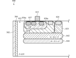
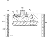
前記画素は、前記画素の側面を形成し、前記画素アレイの上面と前記上面の反対側の前記画素アレイの集光面との間で、前記画素アレイの半導体基板を少なくとも部分的に通って延在している絶縁壁と、
前記上面に隣接するカソード層、及び前記半導体基板内に埋め込まれ、前記上面の反対側の前記カソード層の側面上に隣接して堆積されたアノード層を、含む単一光子アバランシェダイオード(SPAD)と、
前記上面に隣接し、前記SPADと電気的に接続された制御トランジスタであって、前記アノード層の外側に、かつ少なくとも部分的に前記カソード層内に形成され、または少なくとも部分的に前記カソード層と前記上面との間に形成された制御トランジスタと、を備え、
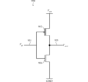
前記アノード層と前記カソード層との間の界面にアバランシェ接合領域が存在し、前記アバランシェ接合領域は、少なくとも部分的に、前記制御トランジスタの下に延長している、画素アレイの画素。 - 前記制御トランジスタが第1の制御トランジスタであり、
前記画素は、第2の制御トランジスタを更に備え、
前記第1の制御トランジスタがゲートトランジスタであり、
前記第2の制御トランジスタは、前記SPADに電気的に接続されているクエンチングトランジスタである、請求項1に記載の画素。 - p-ウェル領域と、前記p-ウェル領域から分離された深いp-ウェル領域と、を更に備え、
前記深いp-ウェル領域は、内部n-ウェル領域を含み、
前記クエンチングトランジスタが、前記内部n-ウェル領域内に形成されたpMOSトランジスタであり、
前記ゲートトランジスタは、前記p-ウェル領域内に形成されたnMOSトランジスタである、請求項2に記載の画素。 - 第1のp-ウェル領域と、第2のp-ウェル領域と、を更に備え、
前記クエンチングトランジスタは、前記第1のp-ウェル領域内に形成された第1のnMOSトランジスタであり、
前記ゲートトランジスタは、前記第2のp-ウェル領域内に形成された第2のnMOSトランジスタである、請求項2に記載の画素。 - 第1のp-ウェル領域を含む第1の深いn-ウェル領域と、第2のp-ウェル領域を含む第2の深いn-ウェル領域と、を更に備え、
前記半導体基板は、n型であり、
前記クエンチングトランジスタが、前記第1のp-ウェル領域内に形成された第1のnMOSトランジスタであり、
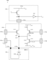
前記ゲートトランジスタは、前記第2のp-ウェル領域に形成された第2のnMOSトランジスタである、請求項2に記載の画素。 - 前記制御トランジスタは、第1の制御トランジスタであり、
前記画素は、第2の制御トランジスタを更に含み、
前記画素は、第3の制御トランジスタを更に含み、
前記第1の制御トランジスタは、前記SPADの第1の電圧ソースとカソードとの間に電気的に接続されたクエンチングトランジスタであり、
前記第2の制御トランジスタは再充電トランジスタであり、
前記第3の制御トランジスタはゲートトランジスタであり、
前記再充電トランジスタは、共通ノードにおいて、第2の電圧ソースと第3の電圧ソースとの間の前記ゲートトランジスタと直列に接続されており、
前記SPADの前記カソードが、前記共通ノードに接続されている、請求項1に記載の画素。 - 第1のn-ウェル領域と、前記第1のn-ウェル領域から分離された第2のn-ウェル領域と、p-ウェル領域と、を含む深いp-ウェル領域を更に備え、
前記ゲートトランジスタは、前記p-ウェル領域に形成されたnMOSトランジスタであり、
前記再充電トランジスタは、前記第1のn-ウェル領域内に形成された第1のpMOSトランジスタであり、
前記クエンチングトランジスタは、前記第2のn-ウェル領域に形成された第2のpMOSトランジスタである、請求項6に記載の画素。 - 第1のn-ウェル領域を含む第1の深いp-ウェル領域と、第2のn-ウェル領域を含む第2の深いp-ウェル領域と、第3のn-ウェル領域を含む第3の深いp-ウェル領域と、を更に備え、
前記ゲートトランジスタは、前記第1のn-ウェル領域に形成された第1のpMOSトランジスタであり、
前記再充電トランジスタは、前記第2のn-ウェル領域内に形成された第2のpMOSトランジスタであり、
前記クエンチングトランジスタは、前記第3のn-ウェル領域に形成された第3のpMOSトランジスタである、請求項6に記載の画素。 - 前記上面から前記半導体基板内に少なくとも部分的に延在している浅いトレンチ絶縁材料を更に備え、
前記浅いトレンチ絶縁材料は、前記画素の第1の領域と、前記画素の第2の領域と、前記画素の第3の領域とを分離しており、
前記クエンチングトランジスタが、前記第1の領域内に形成されており、
前記SPADの前記アノード層及び前記カソード層は、少なくとも部分的に前記第2の領域内に形成されており、
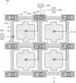
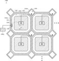
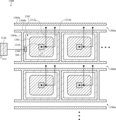
前記ゲートトランジスタ及び前記再充電トランジスタは、前記第3の領域内に形成されている、請求項6に記載の画素。 - 上面及び前記上面の反対側の裏面を有する画素ウエハであって、
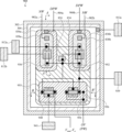
半導体基板と、
画素セルの長方形アレイと、
複数のトランジスタ領域と、
前記画素ウエハの前記上面から前記裏面に近接して前記半導体基板内に延在している深いトレンチ絶縁材料と、を備え、
画素セルの前記長方形アレイの各画素セルが、単一光子アバランシェダイオード(SPAD)を含み、
各トランジスタ領域は、対応する画素セルと関連付けられており、
各トランジスタ領域は、前記トランジスタ領域が関連付けられている前記対応する画素セルの前記SPADと電気的に接続された制御トランジスタを含み、
前記深いトレンチ絶縁材料は、画素セルの前記長方形アレイの各画素セルの周囲の側面を形成し、
各トランジスタ領域は、前記深いトレンチ絶縁材料によって、画素セルの前記長方形アレイの各画素セルから分離されており、
各トランジスタ領域は、画素セルの前記長方形アレイの格子点位置に位置し、かつ画素セルの前記長方形アレイに対して斜めに配向された長方形領域であり、
画素セルの前記長方形アレイの各画素セルの前記SPADは、前記上面に近接するn型カソードと、前記上面の反対側の前記n型カソードの下に形成されたp型アノードとを備えて形成されており、
前記半導体基板は、ドーピング勾配を有するp型であり、
各トランジスタ領域の前記制御トランジスタは、前記トランジスタ領域が関連付けられている前記対応する画素セルの前記SPADの集光動作を制御する、画素ウエハ。 - 前記制御トランジスタが、前記SPADの前記n型カソードと電圧ソースとの間に接続されたpMOSトランジスタである、請求項10に記載の画素ウエハ。
- 複数のトランジスタ領域の第1のトランジスタ領域の前記制御トランジスタは、前記対応する画素セルの前記SPADの前記n型カソードと第1の電圧源との間に接続されたnMOSゲートトランジスタであり、
前記第1のトランジスタ領域が、前記対応する画素セルの前記SPADの前記n型カソードと第2の電圧源との間に接続された、pMOSクエンチングトランジスタを含む、請求項10に記載の画素ウエハ。 - 前記対応する画素セルの前記SPADの前記n型カソードと第3の電圧源との間に接続されたpMOS高速再充電トランジスタを含む第2のトランジスタ領域をさらに含む、請求項12に記載の画素ウエハ。
- 上面及び前記上面の反対側の裏面を有する画素ウエハであって、
半導体基板と、画素セルの長方形アレイとを備え、
少なくとも1つの画素セルは、
前記半導体基板の隣接する異なる層内に形成されたカソード及び埋め込まれたアノードを含む単一光子アバランシェダイオード(SPAD)と、
前記上面に近接して、前記アノードの外側に、かつ少なくとも部分的に前記カソード内に、または少なくとも部分的に前記カソードと前記上面との間に形成された制御トランジスタのグループとを含み、
前記制御トランジスタのグループが、前記SPADの再充電トランジスタと、前記SPADのゲートトランジスタと、前記SPADの前記カソードに接続された入力を有するインバータ回路を形成している第1のトランジスタ及び第2のトランジスタとを含み、
前記アノードと前記カソードとの間の界面にアバランシェ接合領域が存在し、前記アバランシェ接合領域は、少なくとも部分的に、前記制御トランジスタのグループのトランジスタの下に延長している、画素ウエハ。
Priority Applications (2)
| Application Number | Priority Date | Filing Date | Title |
|---|---|---|---|
| JP2024061394A JP7738123B2 (ja) | 2020-09-25 | 2024-04-05 | 積層された単一光子アバランシェダイオード(spad)画素アレイとのトランジスタ統合 |
| JP2025144471A JP2025178258A (ja) | 2020-09-25 | 2025-09-01 | 積層された単一光子アバランシェダイオード(spad)画素アレイとのトランジスタ統合 |
Applications Claiming Priority (4)
| Application Number | Priority Date | Filing Date | Title |
|---|---|---|---|
| US202063083262P | 2020-09-25 | 2020-09-25 | |
| US63/083,262 | 2020-09-25 | ||
| US17/473,855 US12356740B2 (en) | 2020-09-25 | 2021-09-13 | Transistor integration with stacked single-photon avalanche diode (SPAD) pixel arrays |
| US17/473,855 | 2021-09-13 |
Related Child Applications (1)
| Application Number | Title | Priority Date | Filing Date |
|---|---|---|---|
| JP2024061394A Division JP7738123B2 (ja) | 2020-09-25 | 2024-04-05 | 積層された単一光子アバランシェダイオード(spad)画素アレイとのトランジスタ統合 |
Publications (2)
| Publication Number | Publication Date |
|---|---|
| JP2022054459A JP2022054459A (ja) | 2022-04-06 |
| JP7555893B2 true JP7555893B2 (ja) | 2024-09-25 |
Family
ID=80791627
Family Applications (3)
| Application Number | Title | Priority Date | Filing Date |
|---|---|---|---|
| JP2021156525A Active JP7555893B2 (ja) | 2020-09-25 | 2021-09-27 | 積層された単一光子アバランシェダイオード(spad)画素アレイとのトランジスタ統合 |
| JP2024061394A Active JP7738123B2 (ja) | 2020-09-25 | 2024-04-05 | 積層された単一光子アバランシェダイオード(spad)画素アレイとのトランジスタ統合 |
| JP2025144471A Pending JP2025178258A (ja) | 2020-09-25 | 2025-09-01 | 積層された単一光子アバランシェダイオード(spad)画素アレイとのトランジスタ統合 |
Family Applications After (2)
| Application Number | Title | Priority Date | Filing Date |
|---|---|---|---|
| JP2024061394A Active JP7738123B2 (ja) | 2020-09-25 | 2024-04-05 | 積層された単一光子アバランシェダイオード(spad)画素アレイとのトランジスタ統合 |
| JP2025144471A Pending JP2025178258A (ja) | 2020-09-25 | 2025-09-01 | 積層された単一光子アバランシェダイオード(spad)画素アレイとのトランジスタ統合 |
Country Status (4)
| Country | Link |
|---|---|
| US (2) | US12356740B2 (ja) |
| JP (3) | JP7555893B2 (ja) |
| KR (1) | KR102688418B1 (ja) |
| CN (1) | CN114256276A (ja) |
Families Citing this family (7)
| Publication number | Priority date | Publication date | Assignee | Title |
|---|---|---|---|---|
| JP7685533B2 (ja) * | 2021-02-02 | 2025-05-29 | ソニーセミコンダクタソリューションズ株式会社 | 光検出装置、および、測距システム |
| CN114068512A (zh) * | 2021-11-18 | 2022-02-18 | 武汉新芯集成电路制造有限公司 | 半导体器件及半导体芯片 |
| US20230299109A1 (en) * | 2022-03-18 | 2023-09-21 | Taiwan Semiconductor Manufacturing Company, Ltd. | Stacked image sensors and methods of manufacturing thereof |
| US12408466B2 (en) * | 2022-07-11 | 2025-09-02 | Taiwan Semiconductor Manufacturing Company, Ltd. | High-speed readout image sensor |
| WO2024150531A1 (ja) | 2023-01-13 | 2024-07-18 | ソニーセミコンダクタソリューションズ株式会社 | 光検出装置 |
| KR102735202B1 (ko) * | 2023-02-13 | 2024-11-28 | 주식회사 솔리드뷰 | 수광센서를 위한 afe 소자 및 그 제어방법 |
| JP2025009160A (ja) * | 2023-07-07 | 2025-01-20 | ソニーセミコンダクタソリューションズ株式会社 | 光電変換装置 |
Citations (8)
| Publication number | Priority date | Publication date | Assignee | Title |
|---|---|---|---|---|
| US20100127314A1 (en) | 2007-04-24 | 2010-05-27 | Koninklijke Philips Electronics N.V. | Photodiodes and fabrication thereof |
| JP2014225647A (ja) | 2013-04-01 | 2014-12-04 | オムニヴィジョン テクノロジーズ インコーポレイテッド | バイアス深溝分離部を有する高度光子検出装置 |
| JP2016511539A (ja) | 2013-01-31 | 2016-04-14 | アップル インコーポレイテッド | 垂直積層型画像センサ |
| JP2019169643A (ja) | 2018-03-23 | 2019-10-03 | パナソニックIpマネジメント株式会社 | 固体撮像素子 |
| JP2020039017A (ja) | 2018-08-31 | 2020-03-12 | ソニーセミコンダクタソリューションズ株式会社 | 固体撮像装置およびその駆動方法、並びに電子機器 |
| JP2020510308A (ja) | 2017-03-01 | 2020-04-02 | ジーレイ スイッツァーランド エスアー | ウェハ接合に基づく電磁吸収放射線検出器 |
| JP2020143959A (ja) | 2019-03-05 | 2020-09-10 | ソニーセミコンダクタソリューションズ株式会社 | 制御回路および測距システム |
| JP2020155783A (ja) | 2016-09-23 | 2020-09-24 | アップル インコーポレイテッドApple Inc. | 積層背面照射型spadアレイ |
Family Cites Families (263)
| Publication number | Priority date | Publication date | Assignee | Title |
|---|---|---|---|---|
| JPH0668526B2 (ja) | 1986-11-21 | 1994-08-31 | 日産自動車株式会社 | 周波数測定装置 |
| US5056914A (en) | 1990-07-12 | 1991-10-15 | Ball Corporation | Charge integration range detector |
| US5179286A (en) | 1990-10-05 | 1993-01-12 | Mitsubishi Denki K.K. | Distance measuring apparatus receiving echo light pulses |
| JPH04363264A (ja) | 1991-05-27 | 1992-12-16 | Toshiba Corp | 光プリンタ装置 |
| US5610416A (en) | 1995-02-16 | 1997-03-11 | Hewlett-Packard Company | Avalanche photodiode with epitaxially regrown guard rings |
| US6714239B2 (en) | 1997-10-29 | 2004-03-30 | Eastman Kodak Company | Active pixel sensor with programmable color balance |
| US6522395B1 (en) | 1999-04-30 | 2003-02-18 | Canesta, Inc. | Noise reduction techniques suitable for three-dimensional information acquirable with CMOS-compatible image sensor ICS |
| US6323942B1 (en) | 1999-04-30 | 2001-11-27 | Canesta, Inc. | CMOS-compatible three-dimensional image sensor IC |
| JP2001285717A (ja) | 2000-03-29 | 2001-10-12 | Toshiba Corp | 固体撮像装置 |
| TW516184B (en) | 2000-06-20 | 2003-01-01 | Pixelplus Co Ltd | CMOS active pixel for improving sensitivity |
| JP4515617B2 (ja) | 2000-10-23 | 2010-08-04 | 富士フイルム株式会社 | 固体撮像素子およびその駆動方法 |
| US7554067B2 (en) | 2001-05-07 | 2009-06-30 | Panavision Imaging Llc | Scanning imager employing multiple chips with staggered pixels |
| US6791596B2 (en) | 2001-06-28 | 2004-09-14 | Ricoh Company, Ltd. | Method and apparatus for image forming capable of effectively generating pixel clock pulses |
| US7084914B2 (en) | 2001-07-20 | 2006-08-01 | Micron Technology, Inc. | Variable pixel clock electronic shutter control |
| KR100455286B1 (ko) | 2002-01-11 | 2004-11-06 | 삼성전자주식회사 | 생리신호획득 및 해석을 이용한 동물의 상태 파악 방법 및장치 |
| US7906826B2 (en) | 2002-02-05 | 2011-03-15 | E-Phocus | Many million pixel image sensor |
| CN1145245C (zh) | 2002-03-22 | 2004-04-07 | 中国科学院上海光学精密机械研究所 | 激光脉冲时间宽度调节的装置 |
| KR100462182B1 (ko) | 2002-04-15 | 2004-12-16 | 삼성전자주식회사 | Ppg 기반의 심박 검출 장치 및 방법 |
| JP2004048345A (ja) | 2002-07-11 | 2004-02-12 | Niles Co Ltd | 撮像システム |
| GB0216075D0 (en) | 2002-07-11 | 2002-08-21 | Qinetiq Ltd | Photodetector circuits |
| US7525168B2 (en) | 2002-08-27 | 2009-04-28 | E-Phocus, Inc. | CMOS sensor with electrodes across photodetectors at approximately equal potential |
| US7786543B2 (en) | 2002-08-27 | 2010-08-31 | E-Phocus | CDS capable sensor with photon sensing layer on active pixel circuit |
| US7471315B2 (en) | 2003-03-14 | 2008-12-30 | Aptina Imaging Corporation | Apparatus and method for detecting and compensating for illuminant intensity changes within an image |
| JP4131191B2 (ja) | 2003-04-11 | 2008-08-13 | 日本ビクター株式会社 | アバランシェ・フォトダイオード |
| US7075049B2 (en) | 2003-06-11 | 2006-07-11 | Micron Technology, Inc. | Dual conversion gain imagers |
| WO2005020798A2 (en) | 2003-08-27 | 2005-03-10 | Datex-Ohmeda, Inc. | Multi-domain motion estimation and plethysmographic recognition using fuzzy neural-nets |
| US7115855B2 (en) | 2003-09-05 | 2006-10-03 | Micron Technology, Inc. | Image sensor having pinned floating diffusion diode |
| US7154075B2 (en) | 2003-11-13 | 2006-12-26 | Micron Technology, Inc. | Method and apparatus for pixel signal binning and interpolation in column circuits of a sensor circuit |
| US7332786B2 (en) | 2003-11-26 | 2008-02-19 | Micron Technology, Inc. | Anti-blooming storage pixel |
| US7091466B2 (en) | 2003-12-19 | 2006-08-15 | Micron Technology, Inc. | Apparatus and method for pixel binning in an image sensor |
| US7437013B2 (en) | 2003-12-23 | 2008-10-14 | General Instrument Corporation | Directional spatial video noise reduction |
| US7446812B2 (en) | 2004-01-13 | 2008-11-04 | Micron Technology, Inc. | Wide dynamic range operations for imaging |
| US7102117B2 (en) | 2004-06-08 | 2006-09-05 | Eastman Kodak Company | Active pixel sensor cell with integrating varactor and method for using such cell |
| US7825973B2 (en) | 2004-07-16 | 2010-11-02 | Micron Technology, Inc. | Exposure control for image sensors |
| US7880785B2 (en) | 2004-07-21 | 2011-02-01 | Aptina Imaging Corporation | Rod and cone response sensor |
| JP4455215B2 (ja) | 2004-08-06 | 2010-04-21 | キヤノン株式会社 | 撮像装置 |
| US7259413B2 (en) | 2004-09-28 | 2007-08-21 | Micron Technology, Inc. | High dynamic range image sensor |
| US7555158B2 (en) | 2004-12-07 | 2009-06-30 | Electronics And Telecommunications Research Institute | Apparatus for recovering background in image sequence and method thereof |
| US7502054B2 (en) | 2004-12-20 | 2009-03-10 | Pixim, Inc. | Automatic detection of fluorescent flicker in video images |
| US7190039B2 (en) | 2005-02-18 | 2007-03-13 | Micron Technology, Inc. | Microelectronic imagers with shaped image sensors and methods for manufacturing microelectronic imagers |
| JP4855704B2 (ja) | 2005-03-31 | 2012-01-18 | 株式会社東芝 | 固体撮像装置 |
| JP4377840B2 (ja) | 2005-03-31 | 2009-12-02 | イーストマン コダック カンパニー | デジタルカメラ |
| US7443421B2 (en) | 2005-04-05 | 2008-10-28 | Hewlett-Packard Development Company, L.P. | Camera sensor |
| JP4207926B2 (ja) | 2005-05-13 | 2009-01-14 | ソニー株式会社 | フリッカ補正方法、フリッカ補正装置及び撮像装置 |
| TWI429066B (zh) | 2005-06-02 | 2014-03-01 | 新力股份有限公司 | Semiconductor image sensor module and manufacturing method thereof |
| US7415096B2 (en) | 2005-07-26 | 2008-08-19 | Jordan Valley Semiconductors Ltd. | Curved X-ray reflector |
| JP4227152B2 (ja) | 2005-08-02 | 2009-02-18 | 三星電機株式会社 | Cmosイメージセンサの能動ピクセルアレイ |
| KR100775058B1 (ko) | 2005-09-29 | 2007-11-08 | 삼성전자주식회사 | 픽셀 및 이를 이용한 이미지 센서, 그리고 상기 이미지센서를 포함하는 이미지 처리 시스템 |
| US8355117B2 (en) | 2005-12-21 | 2013-01-15 | Ecole Polytechnique Federale De Lausanne | Method and arrangement for measuring the distance to an object |
| US7626626B2 (en) | 2006-01-13 | 2009-12-01 | Micron Technology, Inc. | Method and apparatus providing pixel storage gate charge sensing for electronic stabilization in imagers |
| US7714292B2 (en) | 2006-02-01 | 2010-05-11 | Koninklijke Philips Electronics N.V. | Geiger mode avalanche photodiode |
| JP4796408B2 (ja) | 2006-03-03 | 2011-10-19 | 株式会社リコー | 画像形成装置 |
| US7667400B1 (en) | 2006-06-09 | 2010-02-23 | Array Optronix, Inc. | Back-illuminated Si photomultipliers: structure and fabrication methods |
| US8026966B2 (en) | 2006-08-29 | 2011-09-27 | Micron Technology, Inc. | Method, apparatus and system providing a storage gate pixel with high dynamic range |
| US7773138B2 (en) | 2006-09-13 | 2010-08-10 | Tower Semiconductor Ltd. | Color pattern and pixel level binning for APS image sensor using 2×2 photodiode sharing scheme |
| US8194148B2 (en) | 2006-09-14 | 2012-06-05 | Nikon Corporation | Image processing device, electronic camera and image processing program |
| KR100828943B1 (ko) | 2006-12-19 | 2008-05-13 | (주)실리콘화일 | 3t-4s 스텝 & 리피트 단위 셀 및 상기 단위 셀을 구비한 이미지센서, 데이터 저장 장치, 반도체 공정 마스크, 반도체 웨이퍼 |
| US7742090B2 (en) | 2006-12-22 | 2010-06-22 | Palo Alto Research Center Incorporated | Flexible segmented image sensor |
| US7589316B2 (en) | 2007-01-18 | 2009-09-15 | Ethicon Endo-Surgery, Inc. | Scanning beam imaging with adjustable detector sensitivity or gain |
| US7796171B2 (en) | 2007-02-16 | 2010-09-14 | Flir Advanced Imaging Systems, Inc. | Sensor-based gamma correction of a digital camera |
| KR100835892B1 (ko) | 2007-03-26 | 2008-06-09 | (주)실리콘화일 | 칩 적층 이미지센서 |
| JP4935486B2 (ja) | 2007-04-23 | 2012-05-23 | ソニー株式会社 | 固体撮像装置、固体撮像装置の駆動方法、固体撮像装置の信号処理方法および撮像装置 |
| JP5163935B2 (ja) | 2007-05-17 | 2013-03-13 | ソニー株式会社 | イメージセンサ |
| KR100872991B1 (ko) | 2007-06-25 | 2008-12-08 | 주식회사 동부하이텍 | 이미지센서 및 그 제조방법 |
| JP2009021809A (ja) | 2007-07-11 | 2009-01-29 | Canon Inc | 撮像装置の駆動方法、撮像装置、及び撮像システム |
| JP2009075068A (ja) | 2007-08-08 | 2009-04-09 | Nuflare Technology Inc | パターン検査装置及びパターン検査方法 |
| US7696483B2 (en) | 2007-08-10 | 2010-04-13 | General Electric Company | High DQE photon counting detector using statistical recovery of pile-up events |
| JP2009054870A (ja) | 2007-08-28 | 2009-03-12 | Sanyo Electric Co Ltd | 撮像装置 |
| US7873236B2 (en) | 2007-08-28 | 2011-01-18 | General Electric Company | Systems, methods and apparatus for consistency-constrained filtered backprojection for out-of-focus artifacts in digital tomosythesis |
| KR100887887B1 (ko) | 2007-11-06 | 2009-03-06 | 주식회사 동부하이텍 | 이미지센서 |
| JP5163068B2 (ja) | 2007-11-16 | 2013-03-13 | 株式会社ニコン | 撮像装置 |
| JP4971956B2 (ja) | 2007-11-27 | 2012-07-11 | キヤノン株式会社 | フリッカ補正装置、フリッカ補正方法並びに撮像装置 |
| US8259228B2 (en) | 2007-12-10 | 2012-09-04 | Ati Technologies Ulc | Method and apparatus for high quality video motion adaptive edge-directional deinterlacing |
| US7952635B2 (en) | 2007-12-19 | 2011-05-31 | Teledyne Licensing, Llc | Low noise readout apparatus and method with snapshot shutter and correlated double sampling |
| JP5026951B2 (ja) | 2007-12-26 | 2012-09-19 | オリンパスイメージング株式会社 | 撮像素子の駆動装置、撮像素子の駆動方法、撮像装置、及び撮像素子 |
| US9017748B2 (en) | 2007-12-28 | 2015-04-28 | Kraft Foods Group Brands Llc | Potassium fortification in foodstuffs |
| EP2398055B1 (en) | 2008-01-10 | 2012-12-12 | Stmicroelectronics Sa | Pixel circuit for global electronic shutter |
| US8891790B2 (en) | 2008-01-14 | 2014-11-18 | Apple Inc. | Methods for using an accessory to communicate with an electronic device |
| US8227844B2 (en) | 2008-01-14 | 2012-07-24 | International Business Machines Corporation | Low lag transfer gate device |
| US8874377B1 (en) | 2008-02-29 | 2014-10-28 | The United States Of America As Represented By The Secretary Of The Army | Photon counting based particles detection method and apparatus |
| US8116540B2 (en) | 2008-04-04 | 2012-02-14 | Validity Sensors, Inc. | Apparatus and method for reducing noise in fingerprint sensing circuits |
| JP4494492B2 (ja) | 2008-04-09 | 2010-06-30 | キヤノン株式会社 | 固体撮像装置及び固体撮像装置の駆動方法 |
| BRPI0912721B8 (pt) | 2008-05-14 | 2021-06-22 | Espenusa Holding Llc | unidade de coleta de dados de atividade física com dois ou mais sensores infravermelhos, pelo menos um sensor de temperatura e pelo menos um acelerômetro |
| JP5188275B2 (ja) | 2008-06-06 | 2013-04-24 | キヤノン株式会社 | 固体撮像装置、その駆動方法及び撮像システム |
| US8637875B2 (en) | 2008-07-11 | 2014-01-28 | The Regents Of The University Of California | Single photon IR detectors and their integration with silicon detectors |
| JP5300356B2 (ja) | 2008-07-18 | 2013-09-25 | キヤノン株式会社 | 撮像装置、及び撮像装置の制御方法 |
| KR101467509B1 (ko) | 2008-07-25 | 2014-12-01 | 삼성전자주식회사 | 이미지 센서 및 이미지 센서 동작 방법 |
| US8388346B2 (en) | 2008-08-30 | 2013-03-05 | Nokia Corporation | Tactile feedback |
| US7838956B2 (en) | 2008-12-17 | 2010-11-23 | Eastman Kodak Company | Back illuminated sensor with low crosstalk |
| US8164669B2 (en) | 2008-12-19 | 2012-04-24 | Truesense Imaging, Inc. | Charge-coupled device image sensor with efficient binning of same-color pixels |
| US8686952B2 (en) | 2008-12-23 | 2014-04-01 | Apple Inc. | Multi touch with multi haptics |
| US20100159632A1 (en) | 2008-12-23 | 2010-06-24 | Omnivision Technologies, Inc. | Technique for fabrication of backside illuminated image sensor |
| US8760413B2 (en) | 2009-01-08 | 2014-06-24 | Synaptics Incorporated | Tactile surface |
| US8340407B2 (en) | 2009-01-14 | 2012-12-25 | Cisco Technology, Inc. | System and method for image demosaicing |
| EP2211430A3 (en) | 2009-01-23 | 2015-05-27 | Board of Trustees of Michigan State University | Laser autocorrelation system |
| US8378310B2 (en) | 2009-02-11 | 2013-02-19 | Prismatic Sensors Ab | Image quality in photon counting-mode detector systems |
| US20120159996A1 (en) | 2010-12-28 | 2012-06-28 | Gary Edwin Sutton | Curved sensor formed from silicon fibers |
| US8184188B2 (en) | 2009-03-12 | 2012-05-22 | Micron Technology, Inc. | Methods and apparatus for high dynamic operation of a pixel cell |
| US8140143B2 (en) | 2009-04-16 | 2012-03-20 | Massachusetts Institute Of Technology | Washable wearable biosensor |
| US8089036B2 (en) | 2009-04-30 | 2012-01-03 | Omnivision Technologies, Inc. | Image sensor with global shutter and in pixel storage transistor |
| JP2011004390A (ja) | 2009-05-18 | 2011-01-06 | Canon Inc | 撮像装置、撮像システム、及び撮像装置の駆動方法 |
| US8350940B2 (en) | 2009-06-08 | 2013-01-08 | Aptina Imaging Corporation | Image sensors and color filter arrays for charge summing and interlaced readout modes |
| JP5681176B2 (ja) | 2009-06-22 | 2015-03-04 | トヨタ モーター ヨーロッパ ナームロゼ フェンノートシャップ/ソシエテ アノニム | パルス光による光学式距離計 |
| KR101597785B1 (ko) | 2009-07-14 | 2016-02-25 | 삼성전자주식회사 | 이미지 센서 및 영상 처리 방법 |
| US8755854B2 (en) | 2009-07-31 | 2014-06-17 | Nellcor Puritan Bennett Ireland | Methods and apparatus for producing and using lightly filtered photoplethysmograph signals |
| JP5625284B2 (ja) | 2009-08-10 | 2014-11-19 | ソニー株式会社 | 固体撮像装置、固体撮像装置の駆動方法および電子機器 |
| TWI423246B (zh) | 2009-08-21 | 2014-01-11 | Primax Electronics Ltd | 圖像處理方法及其相關裝置 |
| US8619163B2 (en) | 2009-09-18 | 2013-12-31 | Canon Kabushiki Kaisha | Solid state imaging using a correction parameter for correcting a cross talk between adjacent pixels |
| US9066660B2 (en) | 2009-09-29 | 2015-06-30 | Nellcor Puritan Bennett Ireland | Systems and methods for high-pass filtering a photoplethysmograph signal |
| US8194165B2 (en) | 2009-09-30 | 2012-06-05 | Truesense Imaging, Inc. | Methods for capturing and reading out images from an image sensor |
| JP2011091775A (ja) | 2009-10-26 | 2011-05-06 | Toshiba Corp | 固体撮像装置 |
| US8546737B2 (en) | 2009-10-30 | 2013-10-01 | Invisage Technologies, Inc. | Systems and methods for color binning |
| FI20096232A0 (sv) | 2009-11-23 | 2009-11-23 | Valtion Teknillinen | Fysisk aktivitetsbaserad styrning för en anordning |
| JP2011123149A (ja) | 2009-12-09 | 2011-06-23 | Ricoh Co Ltd | 光走査装置及び画像形成装置 |
| TWI515885B (zh) | 2009-12-25 | 2016-01-01 | 新力股份有限公司 | 半導體元件及其製造方法,及電子裝置 |
| US9870053B2 (en) | 2010-02-08 | 2018-01-16 | Immersion Corporation | Systems and methods for haptic feedback using laterally driven piezoelectric actuators |
| US9451887B2 (en) | 2010-03-31 | 2016-09-27 | Nellcor Puritan Bennett Ireland | Systems and methods for measuring electromechanical delay of the heart |
| JP5641287B2 (ja) | 2010-03-31 | 2014-12-17 | ソニー株式会社 | 固体撮像装置、固体撮像装置の駆動方法、および、電子機器 |
| JP2011216673A (ja) | 2010-03-31 | 2011-10-27 | Sony Corp | 固体撮像装置、固体撮像装置の製造方法、および電子機器 |
| JP5516960B2 (ja) | 2010-04-02 | 2014-06-11 | ソニー株式会社 | 固体撮像装置、固体撮像装置の駆動方法、および、電子機器 |
| WO2011127343A2 (en) | 2010-04-08 | 2011-10-13 | Bae Systems Information And Electronic Systems Integration Inc. | Avalanche photodiode operating voltage selection algorithm |
| JP5602225B2 (ja) | 2010-05-07 | 2014-10-08 | 三菱電機株式会社 | レーザレーダ装置 |
| EP2387229B1 (en) | 2010-05-14 | 2016-04-06 | Casio Computer Co., Ltd. | Image capturing apparatus and camera shake correction method, and computer-readable medium |
| KR101473424B1 (ko) | 2010-06-01 | 2014-12-24 | 볼리 미디어 커뮤니케이션스 (센젠) 캄파니 리미티드 | 다중 스펙트럼 감광소자 및 그 샘플링 방법 |
| KR101198249B1 (ko) | 2010-07-07 | 2012-11-07 | 에스케이하이닉스 주식회사 | 이미지센서의 컬럼 회로 및 픽셀 비닝 회로 |
| WO2012011095A1 (en) | 2010-07-19 | 2012-01-26 | Yeda Research And Development Co. Ltd. | Linear optical characterization of ultrashort optical pulses |
| JP5682174B2 (ja) | 2010-08-09 | 2015-03-11 | ソニー株式会社 | 固体撮像装置とその製造方法、並びに電子機器 |
| US8338856B2 (en) | 2010-08-10 | 2012-12-25 | Omnivision Technologies, Inc. | Backside illuminated image sensor with stressed film |
| JP2012048080A (ja) | 2010-08-30 | 2012-03-08 | Ricoh Co Ltd | 光源装置、光走査装置及び画像形成装置 |
| GB201014843D0 (en) | 2010-09-08 | 2010-10-20 | Univ Edinburgh | Single photon avalanche diode for CMOS circuits |
| US9857469B2 (en) | 2010-10-22 | 2018-01-02 | Heptagon Micro Optics Pte. Ltd. | System and method for multi TOF camera operation using phase hopping |
| JP5589760B2 (ja) | 2010-10-27 | 2014-09-17 | ソニー株式会社 | 画像処理装置、撮像装置、画像処理方法およびプログラム。 |
| DE102010060527B3 (de) | 2010-11-12 | 2012-04-19 | Picoquant Gmbh | Schaltungsanordnung zum Nachweis einzelner Photonen |
| US10120446B2 (en) | 2010-11-19 | 2018-11-06 | Apple Inc. | Haptic input device |
| JP5721405B2 (ja) | 2010-11-22 | 2015-05-20 | キヤノン株式会社 | 撮像システム、その制御方法及びプログラム |
| JP5724322B2 (ja) | 2010-11-24 | 2015-05-27 | ソニー株式会社 | 固体撮像装置の製造方法 |
| GB2485994A (en) | 2010-11-30 | 2012-06-06 | St Microelectronics Res & Dev | Navigation device using a Single Photon Avalanche Diode (SPAD) detector |
| JP5673063B2 (ja) | 2010-12-15 | 2015-02-18 | ソニー株式会社 | 固体撮像素子および駆動方法、並びに電子機器 |
| DE102010061382B4 (de) | 2010-12-21 | 2019-02-14 | Sick Ag | Optoelektronischer Sensor und Verfahren zur Erfassung und Abstandsbestimmung von Objekten |
| GB2486668A (en) | 2010-12-22 | 2012-06-27 | St Microelectronics Res & Dev | Real-time processing method and system for an optical range finder |
| EP2469301A1 (en) | 2010-12-23 | 2012-06-27 | André Borowski | Methods and devices for generating a representation of a 3D scene at very high speed |
| EP2469295A1 (en) | 2010-12-23 | 2012-06-27 | André Borowski | 3D landscape real-time imager and corresponding imaging methods |
| US8723975B2 (en) | 2011-01-24 | 2014-05-13 | Aptina Imaging Corporation | High-dynamic-range imaging devices |
| US8803990B2 (en) | 2011-01-25 | 2014-08-12 | Aptina Imaging Corporation | Imaging system with multiple sensors for producing high-dynamic-range images |
| JP2012169530A (ja) | 2011-02-16 | 2012-09-06 | Sony Corp | 固体撮像装置、および、その製造方法、電子機器 |
| JP5708025B2 (ja) | 2011-02-24 | 2015-04-30 | ソニー株式会社 | 固体撮像装置、および、その製造方法、電子機器 |
| RU2589468C2 (ru) | 2011-04-05 | 2016-07-10 | Конинклейке Филипс Н.В. | Матрица детекторов с аналого-цифровым преобразованием времени, имеющая повышенную временную точность |
| US9088727B2 (en) | 2011-04-06 | 2015-07-21 | Pelco, Inc. | Spatially-varying flicker detection |
| KR101294386B1 (ko) | 2011-04-13 | 2013-08-08 | 엘지이노텍 주식회사 | 픽셀, 픽셀 어레이 및 픽셀 어레이를 포함하는 이미지센서 |
| US8575531B2 (en) | 2011-04-26 | 2013-11-05 | Aptina Imaging Corporation | Image sensor array for back side illumination with global shutter using a junction gate photodiode |
| JP6059722B2 (ja) | 2011-08-03 | 2017-01-11 | コーニンクレッカ フィリップス エヌ ヴェKoninklijke Philips N.V. | デジタルシリコン光電子増倍管アレイに関する位置敏感な読み出しモード |
| JP2013055500A (ja) | 2011-09-02 | 2013-03-21 | Sony Corp | 固体撮像素子およびカメラシステム |
| US8797512B2 (en) | 2011-09-15 | 2014-08-05 | Advanced Scientific Concepts, Inc. | Automatic range corrected flash ladar camera |
| JP5935274B2 (ja) | 2011-09-22 | 2016-06-15 | ソニー株式会社 | 固体撮像装置、固体撮像装置の制御方法および固体撮像装置の制御プログラム |
| GB2494479A (en) | 2011-10-19 | 2013-03-13 | St Microelectronics Res & Dev | A proximity sensor with a cover for directing radiation from a radiation source to a reference radiation detector |
| US8594170B2 (en) | 2011-10-24 | 2013-11-26 | Sigear Europe Sarl | Clock masking scheme in a mixed-signal system |
| WO2013066959A1 (en) | 2011-10-31 | 2013-05-10 | The Trustees Of Columbia University In The City Of New York | Systems and methods for imaging using single photon avalanche diodes |
| JP5764466B2 (ja) | 2011-11-04 | 2015-08-19 | ルネサスエレクトロニクス株式会社 | 固体撮像装置 |
| US8982237B2 (en) | 2011-12-09 | 2015-03-17 | Htc Corporation | Portable electronic device with auto-exposure control adaptive to environment brightness and image capturing method using the same |
| JP6239820B2 (ja) | 2011-12-19 | 2017-11-29 | キヤノン株式会社 | 撮像装置及びその制御方法 |
| JP5497874B2 (ja) | 2011-12-22 | 2014-05-21 | 富士フイルム株式会社 | 放射線画像検出器、放射線画像撮像装置、及び放射線画像撮像システム |
| JP5903894B2 (ja) | 2012-01-06 | 2016-04-13 | 株式会社リコー | 光走査装置及び画像形成装置 |
| FR2985570A1 (fr) | 2012-01-09 | 2013-07-12 | St Microelectronics Grenoble 2 | Dispositif de detection de la proximite d'un objet, comprenant des photodiodes spad |
| EP2624569B1 (en) | 2012-02-06 | 2016-09-28 | Harvest Imaging bvba | Method for correcting image data from an image sensor having image pixels and non-image pixels, and image sensor implementing the same |
| WO2013118111A1 (en) | 2012-02-12 | 2013-08-15 | El-Mul Technologies Ltd. | Position sensitive stem detector |
| JP6151530B2 (ja) | 2012-02-29 | 2017-06-21 | 株式会社半導体エネルギー研究所 | イメージセンサ、カメラ、及び監視システム |
| FR2989518A1 (fr) | 2012-04-13 | 2013-10-18 | St Microelectronics Crolles 2 | Procede de fabrication d'un capteur d'image a surface courbe |
| US9270906B2 (en) | 2012-05-02 | 2016-02-23 | Semiconductor Components Industries, Llc | Exposure time selection using stacked-chip image sensors |
| US10334181B2 (en) | 2012-08-20 | 2019-06-25 | Microsoft Technology Licensing, Llc | Dynamically curved sensor for optical zoom lens |
| US8817154B2 (en) | 2012-08-30 | 2014-08-26 | Omnivision Technologies, Inc. | Image sensor with fixed potential output transistor |
| US9448110B2 (en) | 2012-09-27 | 2016-09-20 | Northrop Grumman Systems Corporation | Three-dimensional hyperspectral imaging systems and methods using a light detection and ranging (LIDAR) focal plane array |
| JP6012375B2 (ja) | 2012-09-28 | 2016-10-25 | 株式会社メガチップス | 画素補間処理装置、撮像装置、プログラムおよび集積回路 |
| JP6017916B2 (ja) | 2012-10-16 | 2016-11-02 | 株式会社豊田中央研究所 | 光検出器 |
| JP6225411B2 (ja) | 2012-10-16 | 2017-11-08 | 株式会社豊田中央研究所 | 光学的測距装置 |
| GB201219781D0 (en) | 2012-11-02 | 2012-12-19 | St Microelectronics Res & Dev | Improvements in time of flight pixel circuits |
| FR2998666B1 (fr) | 2012-11-27 | 2022-01-07 | E2V Semiconductors | Procede de production d'images avec information de profondeur et capteur d'image |
| US9700240B2 (en) | 2012-12-14 | 2017-07-11 | Microsoft Technology Licensing, Llc | Physical activity inference from environmental metrics |
| CN103064076B (zh) | 2012-12-26 | 2014-06-25 | 南京理工大学 | 光子计数三维成像激光雷达距离行走误差校正系统及方法 |
| US9164144B2 (en) | 2012-12-27 | 2015-10-20 | General Electric Company | Characterization and calibration of large area solid state photomultiplier breakdown voltage and/or capacitance |
| GB2510890A (en) | 2013-02-18 | 2014-08-20 | St Microelectronics Res & Dev | Method and apparatus |
| US8934030B2 (en) | 2013-02-20 | 2015-01-13 | Hewlett-Packard Development Company, L.P. | Suppressing flicker in digital images |
| JP6087674B2 (ja) | 2013-02-27 | 2017-03-01 | キヤノン株式会社 | 撮像装置 |
| US9293500B2 (en) | 2013-03-01 | 2016-03-22 | Apple Inc. | Exposure control for image sensors |
| US9276031B2 (en) | 2013-03-04 | 2016-03-01 | Apple Inc. | Photodiode with different electric potential regions for image sensors |
| US9041837B2 (en) | 2013-03-05 | 2015-05-26 | Apple Inc. | Image sensor with reduced blooming |
| KR20140109668A (ko) | 2013-03-06 | 2014-09-16 | 삼성전자주식회사 | 플리커를 검출하기 위한 방법 및 시스템 |
| US9741754B2 (en) | 2013-03-06 | 2017-08-22 | Apple Inc. | Charge transfer circuit with storage nodes in image sensors |
| KR102009189B1 (ko) | 2013-03-12 | 2019-08-09 | 삼성전자주식회사 | 이미지 센서 및 2행 동시 독출 방법 |
| US9549099B2 (en) | 2013-03-12 | 2017-01-17 | Apple Inc. | Hybrid image sensor |
| US9319611B2 (en) | 2013-03-14 | 2016-04-19 | Apple Inc. | Image sensor with flexible pixel summing |
| US9066017B2 (en) | 2013-03-25 | 2015-06-23 | Google Inc. | Viewfinder display based on metering images |
| JP6104049B2 (ja) | 2013-05-21 | 2017-03-29 | オリンパス株式会社 | 画像処理装置、画像処理方法、および画像処理用プログラム |
| US9154750B2 (en) | 2013-05-28 | 2015-10-06 | Omnivision Technologies, Inc. | Correction of image sensor fixed-pattern noise (FPN) due to color filter pattern |
| JP2015012127A (ja) | 2013-06-28 | 2015-01-19 | ソニー株式会社 | 固体撮像素子および電子機器 |
| GB2520232A (en) | 2013-08-06 | 2015-05-20 | Univ Edinburgh | Multiple Event Time to Digital Converter |
| JP6090060B2 (ja) | 2013-08-23 | 2017-03-08 | 株式会社豊田中央研究所 | シングルフォトンアバランシェダイオード |
| US9344649B2 (en) | 2013-08-23 | 2016-05-17 | Semiconductor Components Industries, Llc | Floating point image sensors with different integration times |
| CN103472458B (zh) | 2013-09-16 | 2015-04-15 | 中国科学院上海光学精密机械研究所 | 基于声光扫描的三维视频激光雷达系统 |
| US9596420B2 (en) | 2013-12-05 | 2017-03-14 | Apple Inc. | Image sensor having pixels with different integration periods |
| US9473706B2 (en) | 2013-12-09 | 2016-10-18 | Apple Inc. | Image sensor flicker detection |
| US9312401B2 (en) | 2014-01-15 | 2016-04-12 | Omnivision Technologies, Inc. | Single photon avalanche diode imaging sensor for complementary metal oxide semiconductor stacked chip applications |
| US9331116B2 (en) * | 2014-01-15 | 2016-05-03 | Omnivision Technologies, Inc. | Back side illuminated single photon avalanche diode imaging sensor with high short wavelength detection efficiency |
| KR102135586B1 (ko) | 2014-01-24 | 2020-07-20 | 엘지전자 주식회사 | 이동 단말기 및 이의 제어방법 |
| JP6693880B2 (ja) | 2014-01-29 | 2020-05-13 | エルジー イノテック カンパニー リミテッド | 深さ情報抽出装置および方法 |
| CN103779437A (zh) | 2014-02-17 | 2014-05-07 | 苏州超锐微电子有限公司 | 一种基于标准cmos工艺的单光子级分辨率传感器单元结构 |
| US10276620B2 (en) | 2014-02-27 | 2019-04-30 | Taiwan Semiconductor Manufacturing Co., Ltd. | Image sensor device and method for forming the same |
| US9277144B2 (en) | 2014-03-12 | 2016-03-01 | Apple Inc. | System and method for estimating an ambient light condition using an image sensor and field-of-view compensation |
| US9232150B2 (en) | 2014-03-12 | 2016-01-05 | Apple Inc. | System and method for estimating an ambient light condition using an image sensor |
| US9478030B1 (en) | 2014-03-19 | 2016-10-25 | Amazon Technologies, Inc. | Automatic visual fact extraction |
| CN106165399B (zh) | 2014-04-07 | 2019-08-20 | 三星电子株式会社 | 高分辨率、高帧率、低功率的图像传感器 |
| US9538106B2 (en) | 2014-04-25 | 2017-01-03 | Apple Inc. | Image sensor having a uniform digital power signature |
| US9445018B2 (en) | 2014-05-01 | 2016-09-13 | Semiconductor Components Industries, Llc | Imaging systems with phase detection pixels |
| US9686485B2 (en) | 2014-05-30 | 2017-06-20 | Apple Inc. | Pixel binning in an image sensor |
| US9888198B2 (en) | 2014-06-03 | 2018-02-06 | Semiconductor Components Industries, Llc | Imaging systems having image sensor pixel arrays with sub-pixel resolution capabilities |
| US9209320B1 (en) | 2014-08-07 | 2015-12-08 | Omnivision Technologies, Inc. | Method of fabricating a single photon avalanche diode imaging sensor |
| WO2016033036A2 (en) | 2014-08-26 | 2016-03-03 | Massachusetts Institute Of Technology | Methods and apparatus for three-dimensional (3d) imaging |
| US9685576B2 (en) | 2014-10-03 | 2017-06-20 | Omnivision Technologies, Inc. | Back side illuminated image sensor with guard ring region reflecting structure |
| CN107533210A (zh) | 2015-01-14 | 2018-01-02 | 因维萨热技术公司 | 相位检测自动聚焦 |
| US10217889B2 (en) * | 2015-01-27 | 2019-02-26 | Ladarsystems, Inc. | Clamped avalanche photodiode |
| JP6333189B2 (ja) | 2015-02-09 | 2018-05-30 | 三菱電機株式会社 | レーザ受信装置 |
| CN105991933B (zh) | 2015-02-15 | 2019-11-08 | 比亚迪股份有限公司 | 图像传感器 |
| US9921299B2 (en) | 2015-02-20 | 2018-03-20 | Apple Inc. | Dynamic beam spot size for light beam scanning device |
| US10107914B2 (en) | 2015-02-20 | 2018-10-23 | Apple Inc. | Actuated optical element for light beam scanning device |
| KR20160103302A (ko) | 2015-02-24 | 2016-09-01 | 에스케이하이닉스 주식회사 | 램프전압 제너레이터 및 그를 포함하는 이미지 센싱 장치 |
| CN104810377B (zh) | 2015-03-04 | 2018-03-06 | 南京邮电大学 | 一种高集成度的单光子雪崩二极管探测器阵列单元 |
| KR20160109002A (ko) | 2015-03-09 | 2016-09-21 | 에스케이하이닉스 주식회사 | 출력 극성 변환을 이용한 전치 증폭기 및 그를 이용한 비교기와 아날로그-디지털 변환 장치 |
| EP3070494B1 (de) | 2015-03-18 | 2021-04-28 | Leica Geosystems AG | Elektrooptisches distanzmessverfahren und ebensolcher distanzmesser |
| US9749556B2 (en) | 2015-03-24 | 2017-08-29 | Semiconductor Components Industries, Llc | Imaging systems having image sensor pixel arrays with phase detection capabilities |
| US10145678B2 (en) | 2015-04-20 | 2018-12-04 | Samsung Electronics Co., Ltd. | CMOS image sensor for depth measurement using triangulation with point scan |
| US9661308B1 (en) | 2015-04-20 | 2017-05-23 | Samsung Electronics Co., Ltd. | Increasing tolerance of sensor-scanner misalignment of the 3D camera with epipolar line laser point scanning |
| US9450007B1 (en) | 2015-05-28 | 2016-09-20 | Stmicroelectronics S.R.L. | Integrated circuit with reflective material in trenches and related methods |
| US10620300B2 (en) | 2015-08-20 | 2020-04-14 | Apple Inc. | SPAD array with gated histogram construction |
| US10613225B2 (en) | 2015-09-21 | 2020-04-07 | Kabushiki Kaisha Toshiba | Distance measuring device |
| GB2542811A (en) | 2015-09-30 | 2017-04-05 | Stmicroelectronics (Research & Development) Ltd | Sensing apparatus having a light sensitive detector |
| CN105185796B (zh) | 2015-09-30 | 2018-06-29 | 南京邮电大学 | 一种高探测效率的单光子雪崩二极管探测器阵列单元 |
| US10067224B2 (en) | 2015-10-22 | 2018-09-04 | Stmicroelectronics (Research & Development) Limited | Time to digital converter (TDC) with synchronous output and related methods |
| EP3159711A1 (en) | 2015-10-23 | 2017-04-26 | Xenomatix NV | System and method for determining a distance to an object |
| FR3043797A1 (ja) | 2015-11-16 | 2017-05-19 | Stmicroelectronics (Grenoble 2) Sas | |
| US10078183B2 (en) | 2015-12-11 | 2018-09-18 | Globalfoundries Inc. | Waveguide structures used in phonotics chip packaging |
| CN111239708B (zh) | 2015-12-20 | 2024-01-09 | 苹果公司 | 光检测和测距传感器 |
| US10324171B2 (en) | 2015-12-20 | 2019-06-18 | Apple Inc. | Light detection and ranging sensor |
| EP3206234B1 (en) | 2016-02-09 | 2023-08-09 | ams AG | Semiconductor element with a single photon avalanche diode and method for manufacturing such semiconductor element |
| JP6789653B2 (ja) * | 2016-03-31 | 2020-11-25 | キヤノン株式会社 | 光電変換装置およびカメラ |
| US9985163B2 (en) | 2016-04-13 | 2018-05-29 | Stmicroelectronics (Research & Development) Limited | Single photon avalanche diode having pulse shaping filter |
| US20180341009A1 (en) | 2016-06-23 | 2018-11-29 | Apple Inc. | Multi-range time of flight sensing |
| US10153310B2 (en) | 2016-07-18 | 2018-12-11 | Omnivision Technologies, Inc. | Stacked-chip backside-illuminated SPAD sensor with high fill-factor |
| US10495736B2 (en) | 2016-08-04 | 2019-12-03 | Stmicroelectronics (Research & Development) Limited | Single SPAD array ranging system |
| US10305247B2 (en) | 2016-08-30 | 2019-05-28 | Apple Inc. | Radiation source with a small-angle scanning array |
| FR3056019B1 (fr) | 2016-09-13 | 2018-10-12 | Commissariat A L'energie Atomique Et Aux Energies Alternatives | Photodiode de type spad |
| US10416293B2 (en) | 2016-12-12 | 2019-09-17 | Sensl Technologies Ltd. | Histogram readout method and circuit for determining the time of flight of a photon |
| CN106526612A (zh) | 2016-12-15 | 2017-03-22 | 哈尔滨工业大学 | 一种扫描式光子计数非视域三维成像装置及方法 |
| US10801886B2 (en) | 2017-01-25 | 2020-10-13 | Apple Inc. | SPAD detector having modulated sensitivity |
| US10656251B1 (en) | 2017-01-25 | 2020-05-19 | Apple Inc. | Signal acquisition in a SPAD detector |
| US10962628B1 (en) | 2017-01-26 | 2021-03-30 | Apple Inc. | Spatial temporal weighting in a SPAD detector |
| US10139478B2 (en) | 2017-03-28 | 2018-11-27 | Luminar Technologies, Inc. | Time varying gain in an optical detector operating in a lidar system |
| US11002853B2 (en) | 2017-03-29 | 2021-05-11 | Luminar, Llc | Ultrasonic vibrations on a window in a lidar system |
| US10663595B2 (en) | 2017-03-29 | 2020-05-26 | Luminar Technologies, Inc. | Synchronized multiple sensor head system for a vehicle |
| DE102017207317B4 (de) | 2017-05-02 | 2022-03-03 | Fraunhofer-Gesellschaft zur Förderung der angewandten Forschung e.V. | Vorrichtung zur Ermittlung eines Abstands zu einem Objekt sowie entsprechendes Verfahren |
| CN110869804B (zh) | 2017-07-13 | 2023-11-28 | 苹果公司 | 用于光发射深度传感器的提前-滞后脉冲计数 |
| JP2020034521A (ja) | 2018-08-31 | 2020-03-05 | ソニーセミコンダクタソリューションズ株式会社 | 受光素子および測距システム |
| US11233966B1 (en) | 2018-11-29 | 2022-01-25 | Apple Inc. | Breakdown voltage monitoring for avalanche diodes |
| US11081611B2 (en) * | 2019-05-21 | 2021-08-03 | Hi Llc | Photodetector architectures for efficient fast-gating comprising a control system controlling a current drawn by an array of photodetectors with a single photon avalanche diode |
| JP7638664B2 (ja) * | 2020-01-31 | 2025-03-04 | キヤノン株式会社 | 光電変換装置、光電変換システム、および移動体 |
-
2021
- 2021-09-13 US US17/473,855 patent/US12356740B2/en active Active
- 2021-09-18 CN CN202111097688.6A patent/CN114256276A/zh active Pending
- 2021-09-24 KR KR1020210126248A patent/KR102688418B1/ko active Active
- 2021-09-27 JP JP2021156525A patent/JP7555893B2/ja active Active
-
2024
- 2024-04-05 JP JP2024061394A patent/JP7738123B2/ja active Active
-
2025
- 2025-07-03 US US19/259,835 patent/US20250331322A1/en active Pending
- 2025-09-01 JP JP2025144471A patent/JP2025178258A/ja active Pending
Patent Citations (8)
| Publication number | Priority date | Publication date | Assignee | Title |
|---|---|---|---|---|
| US20100127314A1 (en) | 2007-04-24 | 2010-05-27 | Koninklijke Philips Electronics N.V. | Photodiodes and fabrication thereof |
| JP2016511539A (ja) | 2013-01-31 | 2016-04-14 | アップル インコーポレイテッド | 垂直積層型画像センサ |
| JP2014225647A (ja) | 2013-04-01 | 2014-12-04 | オムニヴィジョン テクノロジーズ インコーポレイテッド | バイアス深溝分離部を有する高度光子検出装置 |
| JP2020155783A (ja) | 2016-09-23 | 2020-09-24 | アップル インコーポレイテッドApple Inc. | 積層背面照射型spadアレイ |
| JP2020510308A (ja) | 2017-03-01 | 2020-04-02 | ジーレイ スイッツァーランド エスアー | ウェハ接合に基づく電磁吸収放射線検出器 |
| JP2019169643A (ja) | 2018-03-23 | 2019-10-03 | パナソニックIpマネジメント株式会社 | 固体撮像素子 |
| JP2020039017A (ja) | 2018-08-31 | 2020-03-12 | ソニーセミコンダクタソリューションズ株式会社 | 固体撮像装置およびその駆動方法、並びに電子機器 |
| JP2020143959A (ja) | 2019-03-05 | 2020-09-10 | ソニーセミコンダクタソリューションズ株式会社 | 制御回路および測距システム |
Also Published As
| Publication number | Publication date |
|---|---|
| CN114256276A (zh) | 2022-03-29 |
| KR20220041761A (ko) | 2022-04-01 |
| KR102688418B1 (ko) | 2024-07-26 |
| US20220102404A1 (en) | 2022-03-31 |
| JP2022054459A (ja) | 2022-04-06 |
| JP2024106992A (ja) | 2024-08-08 |
| JP2025178258A (ja) | 2025-12-05 |
| US12356740B2 (en) | 2025-07-08 |
| JP7738123B2 (ja) | 2025-09-11 |
| US20250331322A1 (en) | 2025-10-23 |
Similar Documents
| Publication | Publication Date | Title |
|---|---|---|
| JP7555893B2 (ja) | 積層された単一光子アバランシェダイオード(spad)画素アレイとのトランジスタ統合 | |
| CN113614932B (zh) | 光检测器 | |
| JP7174932B2 (ja) | 固体撮像素子 | |
| US10985291B2 (en) | Radiation-hard high-speed photodiode device | |
| US11222911B2 (en) | Photoelectric conversion element and solid-state imaging device | |
| EP3355082B1 (en) | Radiation detector panel assembly structure | |
| US20230268372A1 (en) | Stacked cmos image sensor | |
| JP7411916B2 (ja) | 撮像装置 | |
| CN100565892C (zh) | 具有图像传感器的半导体器件和这种器件的制造方法 | |
| CN109564920B (zh) | 半导体集成电路 | |
| KR20210117702A (ko) | 이미지 장치 | |
| KR20210122526A (ko) | 이미지 센서 장치 | |
| JP7199013B2 (ja) | 光検出器 | |
| US20240282788A1 (en) | Integrated circuit and image sensor including the same | |
| Miyoshi | Recent progress in development of SOI pixel detectors | |
| JP2020161775A (ja) | 光検出器 | |
| RU2362237C1 (ru) | Фотоприемная ячейка с вертикальным разделением цветов | |
| CN119923003A (zh) | 图像传感器及其形成方法 | |
| Ratti et al. | CMOS monolithic sensors in a homogeneous 3D process for low energy particle imaging |
Legal Events
| Date | Code | Title | Description |
|---|---|---|---|
| A621 | Written request for application examination |
Free format text: JAPANESE INTERMEDIATE CODE: A621 Effective date: 20211006 |
|
| A977 | Report on retrieval |
Free format text: JAPANESE INTERMEDIATE CODE: A971007 Effective date: 20221028 |
|
| A131 | Notification of reasons for refusal |
Free format text: JAPANESE INTERMEDIATE CODE: A131 Effective date: 20221102 |
|
| A521 | Request for written amendment filed |
Free format text: JAPANESE INTERMEDIATE CODE: A523 Effective date: 20230201 |
|
| A131 | Notification of reasons for refusal |
Free format text: JAPANESE INTERMEDIATE CODE: A131 Effective date: 20230601 |
|
| A521 | Request for written amendment filed |
Free format text: JAPANESE INTERMEDIATE CODE: A523 Effective date: 20230831 |
|
| A02 | Decision of refusal |
Free format text: JAPANESE INTERMEDIATE CODE: A02 Effective date: 20231207 |
|
| A521 | Request for written amendment filed |
Free format text: JAPANESE INTERMEDIATE CODE: A523 Effective date: 20240405 |
|
| A911 | Transfer to examiner for re-examination before appeal (zenchi) |
Free format text: JAPANESE INTERMEDIATE CODE: A911 Effective date: 20240520 |
|
| TRDD | Decision of grant or rejection written | ||
| A01 | Written decision to grant a patent or to grant a registration (utility model) |
Free format text: JAPANESE INTERMEDIATE CODE: A01 Effective date: 20240822 |
|
| A61 | First payment of annual fees (during grant procedure) |
Free format text: JAPANESE INTERMEDIATE CODE: A61 Effective date: 20240911 |
|
| R150 | Certificate of patent or registration of utility model |
Ref document number: 7555893 Country of ref document: JP Free format text: JAPANESE INTERMEDIATE CODE: R150 |