JP4935486B2 - 固体撮像装置、固体撮像装置の駆動方法、固体撮像装置の信号処理方法および撮像装置 - Google Patents
固体撮像装置、固体撮像装置の駆動方法、固体撮像装置の信号処理方法および撮像装置 Download PDFInfo
- Publication number
- JP4935486B2 JP4935486B2 JP2007112652A JP2007112652A JP4935486B2 JP 4935486 B2 JP4935486 B2 JP 4935486B2 JP 2007112652 A JP2007112652 A JP 2007112652A JP 2007112652 A JP2007112652 A JP 2007112652A JP 4935486 B2 JP4935486 B2 JP 4935486B2
- Authority
- JP
- Japan
- Prior art keywords
- pixel
- voltage
- floating diffusion
- signal
- reset
- Prior art date
- Legal status (The legal status is an assumption and is not a legal conclusion. Google has not performed a legal analysis and makes no representation as to the accuracy of the status listed.)
- Expired - Fee Related
Links
Images


Classifications
-
- G—PHYSICS
- G01—MEASURING; TESTING
- G01J—MEASUREMENT OF INTENSITY, VELOCITY, SPECTRAL CONTENT, POLARISATION, PHASE OR PULSE CHARACTERISTICS OF INFRARED, VISIBLE OR ULTRAVIOLET LIGHT; COLORIMETRY; RADIATION PYROMETRY
- G01J1/00—Photometry, e.g. photographic exposure meter
- G01J1/42—Photometry, e.g. photographic exposure meter using electric radiation detectors
- G01J1/44—Electric circuits
-
- H—ELECTRICITY
- H04—ELECTRIC COMMUNICATION TECHNIQUE
- H04N—PICTORIAL COMMUNICATION, e.g. TELEVISION
- H04N25/00—Circuitry of solid-state image sensors [SSIS]; Control thereof
-
- H—ELECTRICITY
- H04—ELECTRIC COMMUNICATION TECHNIQUE
- H04N—PICTORIAL COMMUNICATION, e.g. TELEVISION
- H04N25/00—Circuitry of solid-state image sensors [SSIS]; Control thereof
- H04N25/50—Control of the SSIS exposure
- H04N25/57—Control of the dynamic range
- H04N25/58—Control of the dynamic range involving two or more exposures
- H04N25/581—Control of the dynamic range involving two or more exposures acquired simultaneously
- H04N25/583—Control of the dynamic range involving two or more exposures acquired simultaneously with different integration times
-
- H—ELECTRICITY
- H04—ELECTRIC COMMUNICATION TECHNIQUE
- H04N—PICTORIAL COMMUNICATION, e.g. TELEVISION
- H04N25/00—Circuitry of solid-state image sensors [SSIS]; Control thereof
- H04N25/60—Noise processing, e.g. detecting, correcting, reducing or removing noise
- H04N25/616—Noise processing, e.g. detecting, correcting, reducing or removing noise involving a correlated sampling function, e.g. correlated double sampling [CDS] or triple sampling
-
- H—ELECTRICITY
- H04—ELECTRIC COMMUNICATION TECHNIQUE
- H04N—PICTORIAL COMMUNICATION, e.g. TELEVISION
- H04N25/00—Circuitry of solid-state image sensors [SSIS]; Control thereof
- H04N25/60—Noise processing, e.g. detecting, correcting, reducing or removing noise
- H04N25/63—Noise processing, e.g. detecting, correcting, reducing or removing noise applied to dark current
- H04N25/633—Noise processing, e.g. detecting, correcting, reducing or removing noise applied to dark current by using optical black pixels
-
- H—ELECTRICITY
- H04—ELECTRIC COMMUNICATION TECHNIQUE
- H04N—PICTORIAL COMMUNICATION, e.g. TELEVISION
- H04N25/00—Circuitry of solid-state image sensors [SSIS]; Control thereof
- H04N25/60—Noise processing, e.g. detecting, correcting, reducing or removing noise
- H04N25/65—Noise processing, e.g. detecting, correcting, reducing or removing noise applied to reset noise, e.g. KTC noise related to CMOS structures by techniques other than CDS
-
- H—ELECTRICITY
- H04—ELECTRIC COMMUNICATION TECHNIQUE
- H04N—PICTORIAL COMMUNICATION, e.g. TELEVISION
- H04N25/00—Circuitry of solid-state image sensors [SSIS]; Control thereof
- H04N25/60—Noise processing, e.g. detecting, correcting, reducing or removing noise
- H04N25/67—Noise processing, e.g. detecting, correcting, reducing or removing noise applied to fixed-pattern noise, e.g. non-uniformity of response
- H04N25/671—Noise processing, e.g. detecting, correcting, reducing or removing noise applied to fixed-pattern noise, e.g. non-uniformity of response for non-uniformity detection or correction
- H04N25/673—Noise processing, e.g. detecting, correcting, reducing or removing noise applied to fixed-pattern noise, e.g. non-uniformity of response for non-uniformity detection or correction by using reference sources
-
- H—ELECTRICITY
- H04—ELECTRIC COMMUNICATION TECHNIQUE
- H04N—PICTORIAL COMMUNICATION, e.g. TELEVISION
- H04N25/00—Circuitry of solid-state image sensors [SSIS]; Control thereof
- H04N25/70—SSIS architectures; Circuits associated therewith
- H04N25/76—Addressed sensors, e.g. MOS or CMOS sensors
- H04N25/77—Pixel circuitry, e.g. memories, A/D converters, pixel amplifiers, shared circuits or shared components
- H04N25/771—Pixel circuitry, e.g. memories, A/D converters, pixel amplifiers, shared circuits or shared components comprising storage means other than floating diffusion
-
- H—ELECTRICITY
- H04—ELECTRIC COMMUNICATION TECHNIQUE
- H04N—PICTORIAL COMMUNICATION, e.g. TELEVISION
- H04N25/00—Circuitry of solid-state image sensors [SSIS]; Control thereof
- H04N25/70—SSIS architectures; Circuits associated therewith
- H04N25/76—Addressed sensors, e.g. MOS or CMOS sensors
- H04N25/77—Pixel circuitry, e.g. memories, A/D converters, pixel amplifiers, shared circuits or shared components
- H04N25/778—Pixel circuitry, e.g. memories, A/D converters, pixel amplifiers, shared circuits or shared components comprising amplifiers shared between a plurality of pixels, i.e. at least one part of the amplifier must be on the sensor array itself
-
- H—ELECTRICITY
- H04—ELECTRIC COMMUNICATION TECHNIQUE
- H04N—PICTORIAL COMMUNICATION, e.g. TELEVISION
- H04N25/00—Circuitry of solid-state image sensors [SSIS]; Control thereof
- H04N25/70—SSIS architectures; Circuits associated therewith
- H04N25/76—Addressed sensors, e.g. MOS or CMOS sensors
-
- H—ELECTRICITY
- H10—SEMICONDUCTOR DEVICES; ELECTRIC SOLID-STATE DEVICES NOT OTHERWISE PROVIDED FOR
- H10F—INORGANIC SEMICONDUCTOR DEVICES SENSITIVE TO INFRARED RADIATION, LIGHT, ELECTROMAGNETIC RADIATION OF SHORTER WAVELENGTH OR CORPUSCULAR RADIATION
- H10F39/00—Integrated devices, or assemblies of multiple devices, comprising at least one element covered by group H10F30/00, e.g. radiation detectors comprising photodiode arrays
- H10F39/80—Constructional details of image sensors
- H10F39/802—Geometry or disposition of elements in pixels, e.g. address-lines or gate electrodes
Landscapes
- Engineering & Computer Science (AREA)
- Multimedia (AREA)
- Signal Processing (AREA)
- Physics & Mathematics (AREA)
- General Physics & Mathematics (AREA)
- Spectroscopy & Molecular Physics (AREA)
- Transforming Light Signals Into Electric Signals (AREA)
- Solid State Image Pick-Up Elements (AREA)
Description
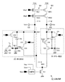
図2は、単位画素20およびダミー画素30の構成の一例を示す回路図である。
単位画素20とダミー画素30は差動回路50を形成している。この差動回路50の具体的な構成について以下に説明する。
図5は、同相帰還回路40の構成の一例を示す回路図である。同相帰還回路40は、その出力端が電流源トランジスタ51のゲート電極に接続されており、差動回路50の差動出力Vom,Vopと外部の電圧源でコントロールされた制御電圧Vcomに基づいて電流源トランジスタ51のゲートバイアスを制御することにより、差動出力Vom,Vopの差分の中心(振幅の中心)が制御電圧Vcomになるように制御を行なう。
続いて、画素アレイ部11における単位画素20、ダミー画素30および同相帰還回路40の動作について、図6のタイミング波形図を用いて説明する。
このように、ソース接地型の増幅トランジスタ24と微小容量の容量素子26を用いて信号の読み出しを行うことによって信号検出感度を高めた単位画素20において、光電変換素子21で光電変換された信号電荷を浮遊拡散容量Cfdに転送する転送トランジスタ22を設けたことにより、先に画素20をリセットしてそのリセットレベルを読み出し、その後に光電変換素子21から信号電荷を転送して信号レベルとして読み出すことで、例えばカラム回路13において相関二重サンプリングによるノイズ除去を実行することができるため、リセットノイズと画素の固定パターンノイズの両方を抑制することができる。
ここで、本実施形態に係る単位画素20では、信号の読み出しに微小容量の容量素子26を用いていることで、差動回路50の単位画素20側とダミー画素30側に、サイズのミスマッチなどによって特性ばらつきがあると、当該特性ばらつきによって出力信号の出力特性に影響が及ぶ懸念がある。
幅範囲を広くすることができる。
また、同様に、信号を検出する容量素子26の容量Cioが微小であるために単位画素20ごとに感度のばらつきが生じる。この感度ばらつきを補正する補正係数は、各画素20に同じ入力を与えたときの各出力の逆数で求めることができる。
ここで、感度ばらつきの補正係数を求めるための第2の方法について、図8のタイミング波形図および図9のポテンシャル図を用いて具体的に説明する。
本実施形態に係る単位画素20、即ち微小容量の容量素子26とソース接地型の増幅トランジスタ24を用いて信号の読み出しを行なう単位画素20は、従来のソースフォロワ読み出しの場合に比べて感度が1桁程度高くなる。そのため、わずかな電荷で画素20からの出力信号が飽和してしまう懸念がある。
以上説明した本実施形態に係る単位画素20については、感度低下が少ないことから、図11に示すように、単位画素20′を光電変換素子21と転送トランジスタ22で構成し、当該単位画素20′を並列に複数配置するとともに、リセットトランジスタ23、増幅トランジスタ24、選択トランジスタ25および容量素子26からなる信号検出回路200を複数の単位画素20′で共有する構成を採ることができる。画素共有化により、読み出し線の寄生容量が減るため、信号の読み出し速度を高速化できる。
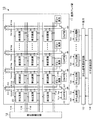
なお、上記実施形態では、可視光の光量に応じた信号電荷を物理量として検知する単位画素が行列状に配置されてなるCMOSイメージセンサに適用した場合を例に挙げて説明したが、本発明はCMOSイメージセンサへの適用に限られるものではなく、画素アレイ部の画素列ごとにカラム回路を配置してなるカラム方式の固体撮像装置全般に対して適用可能である。
図12は、本発明に係る撮像装置の構成の一例を示すブロック図である。図12に示すように、本発明に係る撮像装置60は、レンズ群61を含む光学系、固体撮像装置62、カメラ信号処理回路であるDSP回路63、フレームメモリ64、表示装置65、記録装置66、操作系67および電源系68等を有し、DSP回路63、フレームメモリ64、表示装置65、記録装置66、操作系67および電源系68がバスライン69を介して相互に接続された構成となっている。
Claims (10)
- 光電変換素子と、この光電変換素子で光電変換された信号電荷を浮遊拡散容量に転送する転送トランジスタと、前記浮遊拡散容量と出力ノードの間に接続されたリセットトランジスタと、前記浮遊拡散容量と前記出力ノードの間に接続され、前記浮遊拡散容量と比較して微小な容量の容量素子と、前記容量素子で電圧に変換された信号を読み出す増幅トランジスタとを含む単位画素が配置されてなる画素アレイ部と、
前記画素アレイ部の画素列ごとに設けられ、前記単位画素と同等の特性を有するダミー画素と、
前記単位画素と前記ダミー画素によって形成される差動回路と、
前記リセットトランジスタに対して前記出力ノードを通してリセット電圧を供給するとともに、当該リセット電圧の電圧値が調整可能なリセット電圧供給手段と、
前記リセットトランジスタによるリセット動作が終了した後、前記差動回路の差動出力の差分の中心が、外部の電圧源で調整された制御電圧になるように前記差動回路の電流源の制御を行なう同相帰還回路と
を備えたことを特徴とする固体撮像装置。 - 前記同相帰還回路は、前記リセット電圧供給手段の機能を持っている
ことを特徴とする請求項1記載の固体撮像装置。 - 前記ダミー画素は、前記単位画素に比べてサイズが大きく設計されている
ことを特徴とする請求項1記載の固体撮像装置。 - 光電変換素子と、この光電変換素子で光電変換された信号電荷を浮遊拡散容量に転送する転送トランジスタと、前記浮遊拡散容量と出力ノードの間に接続されたリセットトランジスタと、前記浮遊拡散容量と前記出力ノードの間に接続され、前記浮遊拡散容量と比較して微小な容量の容量素子と、前記容量素子で電圧に変換された信号を読み出す増幅トランジスタとを含む単位画素が配置されてなる画素アレイ部と、
前記画素アレイ部の画素列ごとに設けられ、前記単位画素と同等の特性を有するダミー画素と、
前記単位画素と前記ダミー画素によって形成される差動回路とを備えた固体撮像装置の駆動方法であって、
前記リセットトランジスタに対して前記出力ノードを通して供給するリセット電圧の電圧値を可変とし、
前記リセットトランジスタによるリセット動作の終了後、前記差動回路の差動出力の差分の中心が、外部の電圧源で調整された制御電圧になるように前記差動回路の電流源の制御を行なう
ことを特徴とする固体撮像装置の駆動方法。 - 光電変換素子と、この光電変換素子で光電変換された信号電荷を浮遊拡散容量に転送する転送トランジスタと、前記浮遊拡散容量と出力ノードの間に接続されたリセットトランジスタと、前記浮遊拡散容量と前記出力ノードの間に接続され、前記浮遊拡散容量と比較して微小な容量の容量素子と、前記容量素子で電圧に変換された信号を読み出す増幅トランジスタとを含む単位画素が配置されてなる画素アレイ部と、
前記画素アレイ部の画素列ごとに設けられ、前記単位画素と同等の特性を有するダミー画素と、
前記単位画素と前記ダミー画素によって形成される差動回路とを備えた固体撮像装置の信号処理方法であって、
前記画素アレイ部の各単位画素に同じ入力を与えたときの前記単位画素の各々の出力の逆数を補正係数として求め、
前記補正係数を用いて画素間の感度ばらつきを補正する
ことを特徴とする固体撮像装置の信号処理方法。 - 前記補正係数を求めるに当たって、前記画素アレイ部の各単位画素に対して均一に光を照射し、このときの前記単位画素の各々の出力の逆数を前記補正係数とする
ことを特徴とする請求項5記載の固体撮像装置の信号処理方法。 - 前記補正係数を求めるに当たって、前記転送トランジスタを駆動する転送制御信号の電圧値を徐々に高くして前記光電変換素子で発生した信号電荷を複数回に分けて転送し、初回以外の電荷転送での前記単位画素の各々の出力の逆数を前記補正係数とする
ことを特徴とする請求項5記載の固体撮像装置の信号処理方法。 - 前記初回以外の電荷転送での前記単位画素の各々の出力の平均値の逆数を前記補正係数とする
ことを特徴とする請求項7記載の固体撮像装置の信号処理方法。 - 光電変換素子と、この光電変換素子で光電変換された信号電荷を浮遊拡散容量に転送する転送トランジスタと、前記浮遊拡散容量と出力ノードの間に接続されたリセットトランジスタと、前記浮遊拡散容量と前記出力ノードの間に接続され、前記浮遊拡散容量と比較して微小な容量の容量素子と、前記容量素子で電圧に変換された信号を読み出す増幅トランジスタとを含む単位画素が配置されてなる画素アレイ部と、
前記画素アレイ部の画素列ごとに設けられ、前記単位画素と同等の特性を有するダミー画素と、
前記単位画素と前記ダミー画素によって形成される差動回路とを備えた固体撮像装置の信号処理方法であって、
前記転送トランジスタを駆動する転送制御信号の電圧値を徐々に高くして一単位の蓄積期間に前記光電変換素子で発生した信号電荷を複数回に分けて転送し、
前記複数回の転送によって前記単位画素から出力される各信号を加算処理する
ことを特徴とする固体撮像装置の信号処理方法。 - 光電変換素子と、この光電変換素子で光電変換された信号電荷を浮遊拡散容量に転送する転送トランジスタと、前記浮遊拡散容量と出力ノードの間に接続されたリセットトランジスタと、前記浮遊拡散容量と前記出力ノードの間に接続され、前記浮遊拡散容量と比較して微小な容量の容量素子と、前記容量素子で電圧に変換された信号を読み出す増幅トランジスタとを含む単位画素が配置されてなる固体撮像装置と、
入射光を前記固体撮像装置の撮像面上に結像する光学系とを具備し、
前記固体撮像装置は、
前記画素アレイ部の画素列ごとに設けられ、前記単位画素と同等の特性を有するダミー画素と、
前記単位画素と前記ダミー画素によって形成される差動回路と、
前記リセットトランジスタに対して前記出力ノードを通してリセット電圧を供給するとともに、当該リセット電圧の電圧値が調整可能なリセット電圧供給手段と、
前記リセットトランジスタによるリセット動作が終了した後、前記差動回路の差動出力の差分の中心が、外部の電圧源で調整された制御電圧になるように前記差動回路の電流源の制御を行なう同相帰還回路とを備えた
ことを特徴とする撮像装置。
Priority Applications (7)
| Application Number | Priority Date | Filing Date | Title |
|---|---|---|---|
| JP2007112652A JP4935486B2 (ja) | 2007-04-23 | 2007-04-23 | 固体撮像装置、固体撮像装置の駆動方法、固体撮像装置の信号処理方法および撮像装置 |
| TW097109674A TWI478578B (zh) | 2007-04-23 | 2008-03-19 | 固態影像拾取器件、驅動其之方法、用於其之信號處理方法、以及影像拾取裝置 |
| KR1020080032516A KR101398539B1 (ko) | 2007-04-23 | 2008-04-08 | 고체촬상장치, 고체촬상장치의 구동방법, 고체촬상장치의신호처리방법 및 촬상장치 |
| US12/107,208 US7622699B2 (en) | 2007-04-23 | 2008-04-22 | Solid-state image pickup device, a method of driving the same, a signal processing method for the same, and image pickup apparatus |
| CN2008100954300A CN101296330B (zh) | 2007-04-23 | 2008-04-23 | 固态图像拾取设备及其驱动方法和信号处理方法 |
| US12/565,473 US7897909B2 (en) | 2007-04-23 | 2009-09-23 | Solid-state image pickup device, a method of driving the same, a signal processing method for the same, and image pickup apparatus |
| US13/021,837 US8115159B2 (en) | 2007-04-23 | 2011-02-07 | Solid-state image pickup device including a common phase feedback circuit, a method of driving the same, a signal processing method for the same, and image pickup apparatus |
Applications Claiming Priority (1)
| Application Number | Priority Date | Filing Date | Title |
|---|---|---|---|
| JP2007112652A JP4935486B2 (ja) | 2007-04-23 | 2007-04-23 | 固体撮像装置、固体撮像装置の駆動方法、固体撮像装置の信号処理方法および撮像装置 |
Publications (3)
| Publication Number | Publication Date |
|---|---|
| JP2008271280A JP2008271280A (ja) | 2008-11-06 |
| JP2008271280A5 JP2008271280A5 (ja) | 2010-04-30 |
| JP4935486B2 true JP4935486B2 (ja) | 2012-05-23 |
Family
ID=39871266
Family Applications (1)
| Application Number | Title | Priority Date | Filing Date |
|---|---|---|---|
| JP2007112652A Expired - Fee Related JP4935486B2 (ja) | 2007-04-23 | 2007-04-23 | 固体撮像装置、固体撮像装置の駆動方法、固体撮像装置の信号処理方法および撮像装置 |
Country Status (5)
| Country | Link |
|---|---|
| US (3) | US7622699B2 (ja) |
| JP (1) | JP4935486B2 (ja) |
| KR (1) | KR101398539B1 (ja) |
| CN (1) | CN101296330B (ja) |
| TW (1) | TWI478578B (ja) |
Cited By (1)
| Publication number | Priority date | Publication date | Assignee | Title |
|---|---|---|---|---|
| TWI765481B (zh) * | 2020-06-30 | 2022-05-21 | 敦泰電子股份有限公司 | 指紋畫素單元、指紋顯示裝置及驅動其之積體電路及方法 |
Families Citing this family (92)
| Publication number | Priority date | Publication date | Assignee | Title |
|---|---|---|---|---|
| US8310569B2 (en) * | 2007-05-21 | 2012-11-13 | Aptina Imaging Corporation | Suppression of row-wise noise in CMOS image sensors |
| JP4325703B2 (ja) * | 2007-05-24 | 2009-09-02 | ソニー株式会社 | 固体撮像装置、固体撮像装置の信号処理装置および信号処理方法、ならびに撮像装置 |
| JP5266884B2 (ja) * | 2008-05-30 | 2013-08-21 | ソニー株式会社 | 固体撮像装置、撮像装置、画素駆動方法 |
| JP5359315B2 (ja) * | 2009-01-28 | 2013-12-04 | ソニー株式会社 | 固体撮像装置、固体撮像装置の駆動方法および撮像装置 |
| JP5257134B2 (ja) * | 2009-02-25 | 2013-08-07 | コニカミノルタビジネステクノロジーズ株式会社 | 固体撮像素子およびそれを備えた撮像装置 |
| TWI520030B (zh) * | 2009-05-21 | 2016-02-01 | 原相科技股份有限公司 | 互補式金氧半導體影像感測器及其操作方法 |
| KR101696410B1 (ko) * | 2009-11-11 | 2017-01-16 | 삼성전자주식회사 | 이미지 센서 및 그 동작 방법 |
| US8928644B2 (en) * | 2010-02-19 | 2015-01-06 | Semiconductor Energy Laboratory Co., Ltd. | Display device and method for driving display device |
| CN102214663B (zh) * | 2010-04-09 | 2013-05-01 | 中国科学院微电子研究所 | 一种光学成像器件结构 |
| JP2011238856A (ja) * | 2010-05-12 | 2011-11-24 | Canon Inc | 光電変換装置 |
| JP5672776B2 (ja) * | 2010-06-02 | 2015-02-18 | ソニー株式会社 | 画像処理装置、および画像処理方法、並びにプログラム |
| KR101139477B1 (ko) | 2010-06-25 | 2012-04-30 | 에스케이하이닉스 주식회사 | 이미지 센서 |
| JP5163708B2 (ja) * | 2010-08-16 | 2013-03-13 | 株式会社ニコン | 撮像装置 |
| US20120049047A1 (en) * | 2010-09-01 | 2012-03-01 | Himax Imaging, Inc. | Sensing Devices |
| JP5275312B2 (ja) * | 2010-09-22 | 2013-08-28 | 株式会社東芝 | イメージセンサモジュール及びイメージセンサ |
| CN102610620B (zh) * | 2011-01-20 | 2014-09-10 | 中国科学院微电子研究所 | 一种光学传感器及其内部的成像器件 |
| KR101294445B1 (ko) * | 2011-04-13 | 2013-08-07 | 엘지이노텍 주식회사 | 픽셀, 픽셀 어레이, 픽셀 어레이를 포함하는 이미지센서 및 픽셀 어레이의 구동방법 |
| WO2012144181A1 (ja) * | 2011-04-22 | 2012-10-26 | パナソニック株式会社 | 固体撮像装置及びその駆動方法 |
| JP6021344B2 (ja) | 2011-05-12 | 2016-11-09 | キヤノン株式会社 | 固体撮像装置、固体撮像装置の駆動方法、固体撮像システム |
| JP6150457B2 (ja) * | 2011-05-12 | 2017-06-21 | キヤノン株式会社 | 固体撮像装置、固体撮像装置の駆動方法、固体撮像システム |
| KR101162719B1 (ko) | 2011-05-25 | 2012-07-05 | 서강대학교산학협력단 | 증폭회로 및 그를 구비한 아날로그 디지털 변환회로 |
| JP6021360B2 (ja) | 2012-03-07 | 2016-11-09 | キヤノン株式会社 | 撮像装置、撮像システム、および撮像装置の駆動方法。 |
| WO2013157423A1 (ja) * | 2012-04-19 | 2013-10-24 | 国立大学法人東北大学 | 固体撮像装置 |
| CN102811321B (zh) * | 2012-07-12 | 2014-09-24 | 天津大学 | 低噪声3t像素cmos图像传感器 |
| JP6174902B2 (ja) * | 2012-09-14 | 2017-08-02 | キヤノン株式会社 | 固体撮像装置及びカメラ |
| JP5990080B2 (ja) * | 2012-10-05 | 2016-09-07 | キヤノン株式会社 | 撮像システム、および撮像システムの駆動方法 |
| JP2014099693A (ja) * | 2012-11-13 | 2014-05-29 | Sony Corp | 撮像素子、撮像装置、半導体素子、および読み出し方法 |
| US9276031B2 (en) | 2013-03-04 | 2016-03-01 | Apple Inc. | Photodiode with different electric potential regions for image sensors |
| US9741754B2 (en) * | 2013-03-06 | 2017-08-22 | Apple Inc. | Charge transfer circuit with storage nodes in image sensors |
| US8994867B2 (en) * | 2013-03-15 | 2015-03-31 | Samsung Electronics Co., Ltd. | Image sensor, operating method thereof, and device including the image sensor |
| JP6108936B2 (ja) * | 2013-04-24 | 2017-04-05 | キヤノン株式会社 | 撮像装置、撮像システム、撮像装置の駆動方法 |
| JP5886793B2 (ja) * | 2013-06-11 | 2016-03-16 | 浜松ホトニクス株式会社 | 固体撮像装置 |
| US10285626B1 (en) | 2014-02-14 | 2019-05-14 | Apple Inc. | Activity identification using an optical heart rate monitor |
| JP6274904B2 (ja) | 2014-02-25 | 2018-02-07 | キヤノン株式会社 | 固体撮像装置及び撮像システム |
| JP6418775B2 (ja) * | 2014-04-18 | 2018-11-07 | キヤノン株式会社 | 光電変換装置、撮像システム、および光電変換装置の駆動方法 |
| JP6338440B2 (ja) * | 2014-05-02 | 2018-06-06 | キヤノン株式会社 | 撮像装置の駆動方法、撮像装置、撮像システム |
| US9686485B2 (en) | 2014-05-30 | 2017-06-20 | Apple Inc. | Pixel binning in an image sensor |
| KR102292097B1 (ko) * | 2014-10-01 | 2021-08-24 | 삼성디스플레이 주식회사 | 유기전계발광 표시장치 |
| JP6536788B2 (ja) * | 2015-03-05 | 2019-07-03 | セイコーエプソン株式会社 | 画像読取装置および半導体装置 |
| JP2016201649A (ja) * | 2015-04-09 | 2016-12-01 | キヤノン株式会社 | 撮像装置、撮像システム、および撮像装置の駆動方法 |
| JP6708381B2 (ja) | 2015-08-25 | 2020-06-10 | キヤノン株式会社 | 光電変換装置、および、光電変換システム |
| US9521351B1 (en) | 2015-09-21 | 2016-12-13 | Rambus Inc. | Fractional-readout oversampled image sensor |
| WO2017169484A1 (ja) * | 2016-03-30 | 2017-10-05 | 株式会社ニコン | 撮像素子、撮像装置および半導体メモリ |
| CN107683603B (zh) | 2016-04-15 | 2021-05-14 | 索尼公司 | 固态摄像元件、电子设备和固态摄像元件的控制方法 |
| US9912883B1 (en) | 2016-05-10 | 2018-03-06 | Apple Inc. | Image sensor with calibrated column analog-to-digital converters |
| KR102559953B1 (ko) * | 2016-06-13 | 2023-07-28 | 에스케이하이닉스 주식회사 | 플로팅 확산 영역의 전압 변동 리드아웃 장치 및 그 방법과 그를 이용한 씨모스 이미지 센서 |
| CN106206619B (zh) * | 2016-08-31 | 2019-10-11 | 厦门天马微电子有限公司 | 阵列基板及其驱动方法和显示装置 |
| US9979912B2 (en) * | 2016-09-12 | 2018-05-22 | Semiconductor Components Industries, Llc | Image sensors with power supply noise rejection capabilities |
| EP3516692B1 (en) | 2016-09-23 | 2022-02-16 | Apple Inc. | Stacked backside illuminated spad array |
| JP6886267B2 (ja) * | 2016-10-13 | 2021-06-16 | ソニーセミコンダクタソリューションズ株式会社 | 撮像素子および撮像装置 |
| JP6991704B2 (ja) | 2016-10-26 | 2022-01-12 | ソニーセミコンダクタソリューションズ株式会社 | 固体撮像素子およびその制御方法、並びに電子機器 |
| CN108063905B (zh) * | 2016-11-09 | 2020-04-14 | 京东方科技集团股份有限公司 | 像素感应电路及其驱动方法、图像传感器、电子设备 |
| EP3574344B1 (en) | 2017-01-25 | 2024-06-26 | Apple Inc. | Spad detector having modulated sensitivity |
| US10656251B1 (en) | 2017-01-25 | 2020-05-19 | Apple Inc. | Signal acquisition in a SPAD detector |
| US10962628B1 (en) | 2017-01-26 | 2021-03-30 | Apple Inc. | Spatial temporal weighting in a SPAD detector |
| JP6887856B2 (ja) | 2017-04-11 | 2021-06-16 | ソニーセミコンダクタソリューションズ株式会社 | 固体撮像装置 |
| JP2018182020A (ja) * | 2017-04-11 | 2018-11-15 | ソニーセミコンダクタソリューションズ株式会社 | 固体撮像装置、及び電子機器 |
| JP7055603B2 (ja) * | 2017-04-11 | 2022-04-18 | ソニーセミコンダクタソリューションズ株式会社 | 固体撮像装置、及び、電子機器 |
| WO2018190166A1 (en) * | 2017-04-11 | 2018-10-18 | Sony Semiconductor Solutions Corporation | Solid-state imaging device and electronic apparatus |
| US11343458B2 (en) * | 2017-05-28 | 2022-05-24 | Tohoku University | Light-receiving device and method for reading out signal of light-receiving device |
| US10622538B2 (en) | 2017-07-18 | 2020-04-14 | Apple Inc. | Techniques for providing a haptic output and sensing a haptic input using a piezoelectric body |
| WO2019026429A1 (ja) * | 2017-08-01 | 2019-02-07 | ソニーセミコンダクタソリューションズ株式会社 | 固体撮像素子、撮像装置、および、固体撮像素子の制御方法 |
| WO2019026632A1 (ja) * | 2017-08-02 | 2019-02-07 | ソニーセミコンダクタソリューションズ株式会社 | 固体撮像素子および撮像装置 |
| JP2019041200A (ja) * | 2017-08-24 | 2019-03-14 | ソニーセミコンダクタソリューションズ株式会社 | 固体撮像装置および固体撮像装置の撮像方法、撮像装置、並びに、電子機器 |
| US10440301B2 (en) | 2017-09-08 | 2019-10-08 | Apple Inc. | Image capture device, pixel, and method providing improved phase detection auto-focus performance |
| DE112019001793T5 (de) | 2018-04-04 | 2020-12-31 | Sony Semiconductor Solutions Corporation | 158festkörper-bildgebungsvorrichtung |
| WO2019193801A1 (ja) * | 2018-04-04 | 2019-10-10 | ソニーセミコンダクタソリューションズ株式会社 | 固体撮像素子、電子機器および固体撮像素子の制御方法 |
| JP2019186804A (ja) * | 2018-04-13 | 2019-10-24 | ソニーセミコンダクタソリューションズ株式会社 | 固体撮像素子、撮像装置および固体撮像素子の制御方法 |
| US11451725B2 (en) | 2018-06-27 | 2022-09-20 | Sony Semiconductor Solutions Corporation | Solid-state imaging element, imaging apparatus, and method for controlling solid-state imaging element |
| US10623728B2 (en) * | 2018-07-06 | 2020-04-14 | Stmicroelectronics (Grenoble 2) Sas | Image sensors for advanced driver assistance systems utilizing safety pixels to detect malfunctions |
| US10848693B2 (en) | 2018-07-18 | 2020-11-24 | Apple Inc. | Image flare detection using asymmetric pixels |
| US11019294B2 (en) | 2018-07-18 | 2021-05-25 | Apple Inc. | Seamless readout mode transitions in image sensors |
| JP2020031402A (ja) | 2018-08-24 | 2020-02-27 | ソニーセミコンダクタソリューションズ株式会社 | 固体撮像装置及び電子機器 |
| JP2021182657A (ja) | 2018-08-24 | 2021-11-25 | ソニーセミコンダクタソリューションズ株式会社 | 固体撮像装置及び電子機器 |
| JP2021192395A (ja) | 2018-08-29 | 2021-12-16 | ソニーセミコンダクタソリューションズ株式会社 | 固体撮像素子 |
| JP2022002350A (ja) | 2018-09-19 | 2022-01-06 | ソニーセミコンダクタソリューションズ株式会社 | 固体撮像装置及び電子機器 |
| US11233966B1 (en) | 2018-11-29 | 2022-01-25 | Apple Inc. | Breakdown voltage monitoring for avalanche diodes |
| JP6643656B2 (ja) * | 2018-12-13 | 2020-02-12 | パナソニックIpマネジメント株式会社 | 固体撮像装置 |
| US20200334437A1 (en) * | 2019-04-22 | 2020-10-22 | Himax Technologies Limited | Optical fingerprint detecting system |
| CN111209889A (zh) | 2019-05-16 | 2020-05-29 | 神盾股份有限公司 | 指纹传感器 |
| JP7329963B2 (ja) | 2019-05-17 | 2023-08-21 | ソニーセミコンダクタソリューションズ株式会社 | 固体撮像装置及び電子機器 |
| JP2021125732A (ja) * | 2020-02-03 | 2021-08-30 | ソニーセミコンダクタソリューションズ株式会社 | 固体撮像素子、撮像装置、および、固体撮像素子の制御方法 |
| US11462188B2 (en) | 2020-06-30 | 2022-10-04 | Focal Tech Systems Co., Ltd. | Fingerprint display device and integration integrated circuit and method for driving the same |
| US11563910B2 (en) | 2020-08-04 | 2023-01-24 | Apple Inc. | Image capture devices having phase detection auto-focus pixels |
| EP3985555B1 (en) * | 2020-08-21 | 2023-10-11 | Shenzhen Goodix Technology Co., Ltd. | Image sensor, fingerprint detection apparatus, and electronic device |
| US12356740B2 (en) | 2020-09-25 | 2025-07-08 | Apple Inc. | Transistor integration with stacked single-photon avalanche diode (SPAD) pixel arrays |
| JP7741810B2 (ja) * | 2020-10-08 | 2025-09-18 | ソニーセミコンダクタソリューションズ株式会社 | 固体撮像装置 |
| US11546532B1 (en) | 2021-03-16 | 2023-01-03 | Apple Inc. | Dynamic correlated double sampling for noise rejection in image sensors |
| EP4080874B1 (en) | 2021-04-23 | 2024-12-04 | STMicroelectronics (Research & Development) Limited | Light sensor |
| US12192644B2 (en) | 2021-07-29 | 2025-01-07 | Apple Inc. | Pulse-width modulation pixel sensor |
| US12069384B2 (en) | 2021-09-23 | 2024-08-20 | Apple Inc. | Image capture devices having phase detection auto-focus pixels |
| KR20240060240A (ko) * | 2022-10-28 | 2024-05-08 | 삼성전자주식회사 | 적층형 이미지 센서 |
Family Cites Families (19)
| Publication number | Priority date | Publication date | Assignee | Title |
|---|---|---|---|---|
| US5122881A (en) * | 1988-08-10 | 1992-06-16 | Hitachi, Ltd. | Solid-state imaging device with an amplifying FET in each pixel and an output capacitor in each row |
| US5172249A (en) * | 1989-05-31 | 1992-12-15 | Canon Kabushiki Kaisha | Photoelectric converting apparatus with improved switching to reduce sensor noises |
| JP2545471B2 (ja) * | 1989-11-22 | 1996-10-16 | キヤノン株式会社 | 光電変換装置 |
| JP2884205B2 (ja) * | 1992-01-29 | 1999-04-19 | オリンパス光学工業株式会社 | 固体撮像装置 |
| EP0898419B1 (en) * | 1997-08-15 | 2010-10-27 | Sony Corporation | Solid-state image sensor and method of driving same |
| US6850278B1 (en) * | 1998-11-27 | 2005-02-01 | Canon Kabushiki Kaisha | Solid-state image pickup apparatus |
| JP3592106B2 (ja) * | 1998-11-27 | 2004-11-24 | キヤノン株式会社 | 固体撮像装置およびカメラ |
| JP3667220B2 (ja) * | 1999-10-05 | 2005-07-06 | キヤノン株式会社 | 固体撮像装置、撮像システム及び固体撮像装置の駆動方法 |
| JP2004037382A (ja) * | 2002-07-05 | 2004-02-05 | Toshiba Corp | 放射線検出器及び放射線診断装置 |
| JP3562649B1 (ja) * | 2003-03-20 | 2004-09-08 | 松下電器産業株式会社 | 固体撮像装置およびその駆動方法 |
| US7075049B2 (en) * | 2003-06-11 | 2006-07-11 | Micron Technology, Inc. | Dual conversion gain imagers |
| JP2007506145A (ja) * | 2003-09-23 | 2007-03-15 | イグニス イノベーション インコーポレーテッド | 発光ピクセルのアレイを駆動する回路及び方法 |
| JP4615912B2 (ja) * | 2004-06-30 | 2011-01-19 | オリンパス株式会社 | カメラの焦点演算装置 |
| JP4403045B2 (ja) * | 2004-09-30 | 2010-01-20 | 富士フイルム株式会社 | 放射線画像検出器 |
| JP5019705B2 (ja) * | 2004-11-17 | 2012-09-05 | ソニー株式会社 | 固体撮像装置及び固体撮像装置の駆動方法 |
| JP4561330B2 (ja) * | 2004-11-18 | 2010-10-13 | コニカミノルタホールディングス株式会社 | 固体撮像装置 |
| JP2006352341A (ja) * | 2005-06-14 | 2006-12-28 | Micron Technol Inc | アンチエクリプス回路及びその動作方法 |
| JP4807014B2 (ja) * | 2005-09-02 | 2011-11-02 | ソニー株式会社 | 固体撮像装置、固体撮像装置の駆動方法および撮像装置 |
| JP5167677B2 (ja) * | 2007-04-12 | 2013-03-21 | ソニー株式会社 | 固体撮像装置、固体撮像装置の駆動方法、固体撮像装置の信号処理方法および撮像装置 |
-
2007
- 2007-04-23 JP JP2007112652A patent/JP4935486B2/ja not_active Expired - Fee Related
-
2008
- 2008-03-19 TW TW097109674A patent/TWI478578B/zh not_active IP Right Cessation
- 2008-04-08 KR KR1020080032516A patent/KR101398539B1/ko not_active Expired - Fee Related
- 2008-04-22 US US12/107,208 patent/US7622699B2/en active Active
- 2008-04-23 CN CN2008100954300A patent/CN101296330B/zh active Active
-
2009
- 2009-09-23 US US12/565,473 patent/US7897909B2/en active Active
-
2011
- 2011-02-07 US US13/021,837 patent/US8115159B2/en active Active
Cited By (1)
| Publication number | Priority date | Publication date | Assignee | Title |
|---|---|---|---|---|
| TWI765481B (zh) * | 2020-06-30 | 2022-05-21 | 敦泰電子股份有限公司 | 指紋畫素單元、指紋顯示裝置及驅動其之積體電路及方法 |
Also Published As
| Publication number | Publication date |
|---|---|
| US7897909B2 (en) | 2011-03-01 |
| CN101296330B (zh) | 2010-06-02 |
| US20100013976A1 (en) | 2010-01-21 |
| CN101296330A (zh) | 2008-10-29 |
| US20080258047A1 (en) | 2008-10-23 |
| TW200849987A (en) | 2008-12-16 |
| KR101398539B1 (ko) | 2014-05-26 |
| US7622699B2 (en) | 2009-11-24 |
| TWI478578B (zh) | 2015-03-21 |
| US8115159B2 (en) | 2012-02-14 |
| JP2008271280A (ja) | 2008-11-06 |
| KR20080095175A (ko) | 2008-10-28 |
| US20110127409A1 (en) | 2011-06-02 |
Similar Documents
| Publication | Publication Date | Title |
|---|---|---|
| JP4935486B2 (ja) | 固体撮像装置、固体撮像装置の駆動方法、固体撮像装置の信号処理方法および撮像装置 | |
| JP5167677B2 (ja) | 固体撮像装置、固体撮像装置の駆動方法、固体撮像装置の信号処理方法および撮像装置 | |
| US8089530B2 (en) | Solid-state image pickup apparatus, drive method for the solid-state image pickup apparatus, and image pickup apparatus | |
| JP4529834B2 (ja) | 固体撮像装置、固体撮像装置の駆動方法および撮像装置 | |
| JP5552858B2 (ja) | 固体撮像装置、固体撮像装置の駆動方法、及び、電子機器 | |
| US7616146B2 (en) | A/D conversion circuit, control method thereof, solid-state imaging device, and imaging apparatus | |
| JP5034610B2 (ja) | 固体撮像装置、固体撮像装置の信号処理方法および撮像装置 | |
| US20210092317A1 (en) | Solid-state imaging device, control method thereof, and electronic apparatus | |
| JP6083611B2 (ja) | 固体撮像装置及び撮像装置 | |
| JP6164797B2 (ja) | 信号受信部テスト回路、撮像装置、信号受信部テスト方法、撮像装置のテスト方法 | |
| US20160065871A1 (en) | Solid-state image pickup apparatus, signal processing method for a solid-state image pickup apparatus, and electronic apparatus | |
| US20120008177A1 (en) | Solid-state imaging apparatus and imaging system | |
| WO2012144181A1 (ja) | 固体撮像装置及びその駆動方法 | |
| JP2013051527A (ja) | 固体撮像装置及び撮像装置 | |
| JP2014216794A (ja) | 放射線撮像装置及び放射線検査装置 | |
| CN113728620B (zh) | 差量视觉传感器 | |
| WO2019026632A1 (ja) | 固体撮像素子および撮像装置 | |
| JP4956750B2 (ja) | イメージセンサのための画素及びイメージセンサデバイス | |
| JP2013143636A (ja) | 固体撮像装置、固体撮像装置の信号処理方法、及び、電子機器 | |
| JP2012109888A (ja) | 固体撮像装置 | |
| JP6422319B2 (ja) | 撮像装置、及びそれを用いた撮像システム | |
| WO2015111370A1 (ja) | 固体撮像装置及び撮像装置 | |
| CN115811668A (zh) | 有源像素传感器、显示面板、显示装置和平板探测装置 |
Legal Events
| Date | Code | Title | Description |
|---|---|---|---|
| RD02 | Notification of acceptance of power of attorney |
Free format text: JAPANESE INTERMEDIATE CODE: A7422 Effective date: 20091007 |
|
| RD04 | Notification of resignation of power of attorney |
Free format text: JAPANESE INTERMEDIATE CODE: A7424 Effective date: 20091016 |
|
| A521 | Request for written amendment filed |
Free format text: JAPANESE INTERMEDIATE CODE: A523 Effective date: 20100315 |
|
| A621 | Written request for application examination |
Free format text: JAPANESE INTERMEDIATE CODE: A621 Effective date: 20100315 |
|
| A977 | Report on retrieval |
Free format text: JAPANESE INTERMEDIATE CODE: A971007 Effective date: 20120119 |
|
| TRDD | Decision of grant or rejection written | ||
| A01 | Written decision to grant a patent or to grant a registration (utility model) |
Free format text: JAPANESE INTERMEDIATE CODE: A01 Effective date: 20120124 |
|
| A01 | Written decision to grant a patent or to grant a registration (utility model) |
Free format text: JAPANESE INTERMEDIATE CODE: A01 |
|
| A61 | First payment of annual fees (during grant procedure) |
Free format text: JAPANESE INTERMEDIATE CODE: A61 Effective date: 20120206 |
|
| FPAY | Renewal fee payment (event date is renewal date of database) |
Free format text: PAYMENT UNTIL: 20150302 Year of fee payment: 3 |
|
| FPAY | Renewal fee payment (event date is renewal date of database) |
Free format text: PAYMENT UNTIL: 20150302 Year of fee payment: 3 |
|
| R250 | Receipt of annual fees |
Free format text: JAPANESE INTERMEDIATE CODE: R250 |
|
| LAPS | Cancellation because of no payment of annual fees |