JP7555893B2 - Transistor integration with stacked single-photon avalanche diode (SPAD) pixel arrays - Google Patents
Transistor integration with stacked single-photon avalanche diode (SPAD) pixel arrays Download PDFInfo
- Publication number
- JP7555893B2 JP7555893B2 JP2021156525A JP2021156525A JP7555893B2 JP 7555893 B2 JP7555893 B2 JP 7555893B2 JP 2021156525 A JP2021156525 A JP 2021156525A JP 2021156525 A JP2021156525 A JP 2021156525A JP 7555893 B2 JP7555893 B2 JP 7555893B2
- Authority
- JP
- Japan
- Prior art keywords
- transistor
- pixel
- spad
- well region
- wafer
- Prior art date
- Legal status (The legal status is an assumption and is not a legal conclusion. Google has not performed a legal analysis and makes no representation as to the accuracy of the status listed.)
- Active
Links
Images


Classifications
-
- H—ELECTRICITY
- H10—SEMICONDUCTOR DEVICES; ELECTRIC SOLID-STATE DEVICES NOT OTHERWISE PROVIDED FOR
- H10F—INORGANIC SEMICONDUCTOR DEVICES SENSITIVE TO INFRARED RADIATION, LIGHT, ELECTROMAGNETIC RADIATION OF SHORTER WAVELENGTH OR CORPUSCULAR RADIATION
- H10F39/00—Integrated devices, or assemblies of multiple devices, comprising at least one element covered by group H10F30/00, e.g. radiation detectors comprising photodiode arrays
- H10F39/80—Constructional details of image sensors
- H10F39/803—Pixels having integrated switching, control, storage or amplification elements
- H10F39/8033—Photosensitive area
-
- H—ELECTRICITY
- H10—SEMICONDUCTOR DEVICES; ELECTRIC SOLID-STATE DEVICES NOT OTHERWISE PROVIDED FOR
- H10F—INORGANIC SEMICONDUCTOR DEVICES SENSITIVE TO INFRARED RADIATION, LIGHT, ELECTROMAGNETIC RADIATION OF SHORTER WAVELENGTH OR CORPUSCULAR RADIATION
- H10F30/00—Individual radiation-sensitive semiconductor devices in which radiation controls the flow of current through the devices, e.g. photodetectors
- H10F30/20—Individual radiation-sensitive semiconductor devices in which radiation controls the flow of current through the devices, e.g. photodetectors the devices having potential barriers, e.g. phototransistors
- H10F30/21—Individual radiation-sensitive semiconductor devices in which radiation controls the flow of current through the devices, e.g. photodetectors the devices having potential barriers, e.g. phototransistors the devices being sensitive to infrared, visible or ultraviolet radiation
- H10F30/22—Individual radiation-sensitive semiconductor devices in which radiation controls the flow of current through the devices, e.g. photodetectors the devices having potential barriers, e.g. phototransistors the devices being sensitive to infrared, visible or ultraviolet radiation the devices having only one potential barrier, e.g. photodiodes
- H10F30/225—Individual radiation-sensitive semiconductor devices in which radiation controls the flow of current through the devices, e.g. photodetectors the devices having potential barriers, e.g. phototransistors the devices being sensitive to infrared, visible or ultraviolet radiation the devices having only one potential barrier, e.g. photodiodes the potential barrier working in avalanche mode, e.g. avalanche photodiodes
-
- H—ELECTRICITY
- H10—SEMICONDUCTOR DEVICES; ELECTRIC SOLID-STATE DEVICES NOT OTHERWISE PROVIDED FOR
- H10F—INORGANIC SEMICONDUCTOR DEVICES SENSITIVE TO INFRARED RADIATION, LIGHT, ELECTROMAGNETIC RADIATION OF SHORTER WAVELENGTH OR CORPUSCULAR RADIATION
- H10F39/00—Integrated devices, or assemblies of multiple devices, comprising at least one element covered by group H10F30/00, e.g. radiation detectors comprising photodiode arrays
- H10F39/80—Constructional details of image sensors
- H10F39/802—Geometry or disposition of elements in pixels, e.g. address-lines or gate electrodes
-
- H—ELECTRICITY
- H10—SEMICONDUCTOR DEVICES; ELECTRIC SOLID-STATE DEVICES NOT OTHERWISE PROVIDED FOR
- H10F—INORGANIC SEMICONDUCTOR DEVICES SENSITIVE TO INFRARED RADIATION, LIGHT, ELECTROMAGNETIC RADIATION OF SHORTER WAVELENGTH OR CORPUSCULAR RADIATION
- H10F39/00—Integrated devices, or assemblies of multiple devices, comprising at least one element covered by group H10F30/00, e.g. radiation detectors comprising photodiode arrays
- H10F39/80—Constructional details of image sensors
- H10F39/803—Pixels having integrated switching, control, storage or amplification elements
- H10F39/8037—Pixels having integrated switching, control, storage or amplification elements the integrated elements comprising a transistor
-
- H—ELECTRICITY
- H10—SEMICONDUCTOR DEVICES; ELECTRIC SOLID-STATE DEVICES NOT OTHERWISE PROVIDED FOR
- H10F—INORGANIC SEMICONDUCTOR DEVICES SENSITIVE TO INFRARED RADIATION, LIGHT, ELECTROMAGNETIC RADIATION OF SHORTER WAVELENGTH OR CORPUSCULAR RADIATION
- H10F39/00—Integrated devices, or assemblies of multiple devices, comprising at least one element covered by group H10F30/00, e.g. radiation detectors comprising photodiode arrays
- H10F39/80—Constructional details of image sensors
- H10F39/807—Pixel isolation structures
-
- H—ELECTRICITY
- H10—SEMICONDUCTOR DEVICES; ELECTRIC SOLID-STATE DEVICES NOT OTHERWISE PROVIDED FOR
- H10F—INORGANIC SEMICONDUCTOR DEVICES SENSITIVE TO INFRARED RADIATION, LIGHT, ELECTROMAGNETIC RADIATION OF SHORTER WAVELENGTH OR CORPUSCULAR RADIATION
- H10F39/00—Integrated devices, or assemblies of multiple devices, comprising at least one element covered by group H10F30/00, e.g. radiation detectors comprising photodiode arrays
- H10F39/80—Constructional details of image sensors
- H10F39/809—Constructional details of image sensors of hybrid image sensors
-
- H—ELECTRICITY
- H10—SEMICONDUCTOR DEVICES; ELECTRIC SOLID-STATE DEVICES NOT OTHERWISE PROVIDED FOR
- H10F—INORGANIC SEMICONDUCTOR DEVICES SENSITIVE TO INFRARED RADIATION, LIGHT, ELECTROMAGNETIC RADIATION OF SHORTER WAVELENGTH OR CORPUSCULAR RADIATION
- H10F39/00—Integrated devices, or assemblies of multiple devices, comprising at least one element covered by group H10F30/00, e.g. radiation detectors comprising photodiode arrays
- H10F39/80—Constructional details of image sensors
- H10F39/811—Interconnections
-
- H—ELECTRICITY
- H10—SEMICONDUCTOR DEVICES; ELECTRIC SOLID-STATE DEVICES NOT OTHERWISE PROVIDED FOR
- H10F—INORGANIC SEMICONDUCTOR DEVICES SENSITIVE TO INFRARED RADIATION, LIGHT, ELECTROMAGNETIC RADIATION OF SHORTER WAVELENGTH OR CORPUSCULAR RADIATION
- H10F39/00—Integrated devices, or assemblies of multiple devices, comprising at least one element covered by group H10F30/00, e.g. radiation detectors comprising photodiode arrays
- H10F39/10—Integrated devices
- H10F39/12—Image sensors
- H10F39/18—Complementary metal-oxide-semiconductor [CMOS] image sensors; Photodiode array image sensors
Landscapes
- Solid State Image Pick-Up Elements (AREA)
- Metal-Oxide And Bipolar Metal-Oxide Semiconductor Integrated Circuits (AREA)
- Light Receiving Elements (AREA)
Description
本開示は、概して、光検出器、集光エレメント、又は光検出エレメントとして単一光子アバランシェダイオード(SPAD)を有する画素アレイを含む画像センサに関する。 The present disclosure generally relates to image sensors that include pixel arrays having single photon avalanche diodes (SPADs) as photodetectors, light collecting elements, or light detecting elements.
(関連出願の相互参照)
本出願は、非暫定的であり、2020年9月25日に出願された米国仮特許出願第No.63/083,262号の35 U.S.C.§119(e)の下で利益を主張するものであり、その内容は、本明細書に完全に開示されているかのように参照により本明細書に組み込まれる。
CROSS-REFERENCE TO RELATED APPLICATIONS
This application is non-provisional and claims the benefit under 35 U.S.C. §119(e) of U.S. Provisional Patent Application No. 63/083,262, filed September 25, 2020, the contents of which are incorporated by reference herein as if fully disclosed herein.
電子イメージング又はカメラデバイスは、現在、セル式電話、タブレット又はデスクトップコンピュータ、携帯情報端末などの様々な種類の電子デバイス上で一般的である。これらのイメージングデバイスは、個々の集光センサのアレイ、又は画素のみを使用する場合がある。画素は、多くの場合、半導体ベースであり、受信した光を、電気信号に変換し全画像のそれぞれの部分を生成するように処理される。 Electronic imaging or camera devices are now common on many types of electronic devices, such as cell phones, tablet or desktop computers, personal digital assistants, etc. These imaging devices may only use an array of individual light-gathering sensors, or pixels. The pixels are often semiconductor-based and are processed to convert the light they receive into electrical signals that generate their respective portions of the overall image.
個々の画素はそれぞれ、画素の光感知又はイメージング動作を制御する付随回路(例えば、電源ライン、クエンチング又はゲートトランジスタなどの制御エレクトロニクス、及びその他の構成要素又は回路)と接続され得る。画素の付随回路及び集光半導体部分の配置方法は、画素の集光能力に影響を及ぼし得る。画素の付随回路及び集光半導体部分をどのように配置するかは、電子イメージングデバイス又はカメラデバイスに含まれるウエハの数をより良く使用又は決定することができる。いくつかの実施形態では、画素アレイは、第1のウエハが接合される第2のウエハ上に実装される付随回路と共に、第1のウエハの一部として実装され得る。他の実施形態では、画素アレイは、第1のウエハの一部として実装され、画素の制御又は他の回路構成要素を含む第2のウエハと接合又は結合されてもよく、第2のウエハは、供給及び論理構成要素並びに回路を含む第3のウエハと接合又は結合され得る。 Each individual pixel may be connected with associated circuitry (e.g., power lines, control electronics such as quenching or gate transistors, and other components or circuits) that control the light sensing or imaging operation of the pixel. The manner in which the pixel's associated circuitry and light-collecting semiconductor portion are arranged may affect the light-collecting ability of the pixel. How the pixel's associated circuitry and light-collecting semiconductor portion are arranged may better use or determine the number of wafers included in the electronic imaging or camera device. In some embodiments, the pixel array may be implemented as part of a first wafer, with associated circuitry implemented on a second wafer to which the first wafer is bonded. In other embodiments, the pixel array may be implemented as part of the first wafer and bonded or joined with a second wafer containing pixel control or other circuit components, and the second wafer may be bonded or joined with a third wafer containing supply and logic components and circuits.
この概要は、以下の「発明を実施するための形態」のセクションにおいて更に説明される、選択された概念を、単純化した形で紹介するために提供される。この概要は、クレームされている主題の主要な特徴又は本質的な特徴を特定することを意図されておらず、また、クレームされている主題の範囲の決定を支援するものとして使用されることも意図されていない。 This Summary is provided to introduce selected concepts in a simplified form that are further described in the Detailed Description section below. This Summary is not intended to identify key features or essential features of the claimed subject matter, nor is it intended to be used as an aid in determining the scope of the claimed subject matter.
光検出器、光センサ若しくは画像センサ、それらの内部構成要素、及びそれらの内部構成要素の配置についてデバイス、システム、及び構造体が本明細書に開示される。画像センサは、光検出器が単一光子アバランシェダイオード(SPAD)を含む画素アレイを含み得る。画像センサは、画素ウエハ及び論理及び/又は制御回路ウエハなど、1つ以上の別個に作製されたウエハ又はチップを接続又は結合することによって形成されてもよい。 Disclosed herein are devices, systems, and structures for photodetectors, photosensors, or image sensors, their internal components, and arrangements of their internal components. The image sensor may include a pixel array in which the photodetectors include single photon avalanche diodes (SPADs). The image sensor may be formed by connecting or bonding one or more separately fabricated wafers or chips, such as a pixel wafer and a logic and/or control circuit wafer.
様々な実装及び実施形態は、SPADの内部構造化、並びにSPADの様々な供給及び/又は制御トランジスタの位置決めを対象とする。特定の供給及び制御トランジスタは、それぞれのSPADに近接して画素ウエハ上に配置されてもよく、又はいくつかの実施形態では、専用ウエハ上に別々に配置され得る。 Various implementations and embodiments are directed to the internal structuring of the SPADs and the positioning of the various supply and/or control transistors of the SPADs. The particular supply and control transistors may be located on the pixel wafer in close proximity to the respective SPADs, or in some embodiments may be located separately on a dedicated wafer.
より具体的には、実施形態の第1のセットには、画素アレイの構造が開示される。1つ以上の画素は、SPAD、並びに画素内に形成され、SPADと動作可能に接続された1つ以上の制御トランジスタを含むことができる。制御トランジスタは、画素アレイの半導体基板内に形成され、画素は画素の集光面とは反対側の画素の上面に隣接し得る。画素は、画素の上面から画素の集光面まで少なくとも部分的に延在している絶縁壁の間に配置され得る。SPADのアノード層は、半導体基板内に形成され得、基板はドーピング勾配で形成され得る。第1のファミリー内の特定の実施形態は、1つ、2つ、又は3つの制御トランジスタを有する実施形態を説明する。 More specifically, in a first set of embodiments, pixel array structures are disclosed. One or more pixels may include a SPAD and one or more control transistors formed in the pixel and operatively connected to the SPAD. The control transistors may be formed in a semiconductor substrate of the pixel array, and the pixels may be adjacent to a top surface of the pixel opposite the light collecting surface of the pixel. The pixels may be disposed between insulating walls that extend at least partially from the top surface of the pixel to the light collecting surface of the pixel. An anode layer of the SPAD may be formed in the semiconductor substrate, and the substrate may be formed with a doping gradient. Particular embodiments in the first family describe embodiments having one, two, or three control transistors.
別の実施形態のセットは、長方形アレイとして配置された複数の画素セル及び複数のトランジスタ領域を有する、半導体基板内に形成された画素ウエハを説明する。画素アレイの各画素は、SPADを含み、少なくとも1つの制御トランジスタが各トランジスタ領域内に形成される。深いトレンチ絶縁壁は、画素ウエハの上面から半導体基板の中に、又は上面と反対側の画素ウエハの裏面の近くまで延在し得る。深いトレンチ絶縁壁は、トランジスタ領域を画素セルから分離している。各画素セルのSPADは、上面に近接するn型カソード、及び上面と反対側のn型カソードの下に形成されたp型アノードによって形成される。半導体基板は、ドーピング勾配を有するp型半導体であり得る。 Another set of embodiments describes a pixel wafer formed in a semiconductor substrate having a plurality of pixel cells and a plurality of transistor regions arranged in a rectangular array. Each pixel of the pixel array includes a SPAD, and at least one control transistor is formed in each transistor region. Deep trench isolation walls may extend from a top surface of the pixel wafer into the semiconductor substrate or near a back surface of the pixel wafer opposite the top surface. The deep trench isolation walls separate the transistor regions from the pixel cells. The SPAD of each pixel cell is formed by an n-type cathode adjacent the top surface and a p-type anode formed below the n-type cathode opposite the top surface. The semiconductor substrate may be a p-type semiconductor with a doping gradient.
別の一組の実施形態は、画素セルのアレイを含む画素ウエハと、画素ウエハに接合された第1の側面を有する制御トランジスタウエハと、第1の側面とは反対側の制御トランジスタウエハの第2の側面に接合された論理ウエハと、を含む、光検出器デバイスを説明する。画素ウエハ内の画素セルのアレイの各画素セルは、SPADを含む。制御トランジスタウエハは、各画素セルに対して、それぞれの制御トランジスタ用の、少なくとも再充電トランジスタ、ゲートトランジスタ、及びクエンチングトランジスタを含む制御トランジスタを含む。制御トランジスタは、対応する画素のSPADの光検出動作を制御することができる。論理ウエハは、光検出動作に基づいて、制御トランジスタウエハからの相互接続パッドを介して電気信号を受信し得る回路構成要素を含み得る。
本開示は、添付の図面と併せて以下の詳細な説明によって容易に理解され、同様の参照番号は同様の構造要素を示す。
Another set of embodiments describes a photodetector device including a pixel wafer including an array of pixel cells, a control transistor wafer having a first side bonded to the pixel wafer, and a logic wafer bonded to a second side of the control transistor wafer opposite the first side. Each pixel cell of the array of pixel cells in the pixel wafer includes a SPAD. The control transistor wafer includes, for each pixel cell, a control transistor including at least a recharge transistor, a gating transistor, and a quenching transistor for the respective control transistor. The control transistor can control a photodetection operation of the SPAD of the corresponding pixel. The logic wafer can include circuitry that can receive an electrical signal via an interconnect pad from the control transistor wafer based on the photodetection operation.
The present disclosure will be readily understood by the following detailed description in conjunction with the accompanying drawings, in which like reference numerals indicate like structural elements, and in which:
添付の図でのクロスハッチング又はシェーディングの使用は、概して、隣り合う要素間の境界を明らかにし、図の視認性も促進するためにも提供される。したがって、クロスハッチング又はシェーディングの存在も不在も、添付の図に示される任意の要素に関する特定の材料、材料特性、要素の割合、要素の寸法、同様に図示されている要素の共通点、又は任意の他の特質、属性、若しくは特性についてのいかなる選好又は要件も伝達又は指示するものではない。 The use of cross-hatching or shading in the accompanying figures is generally provided to clarify boundaries between adjacent elements and also to facilitate visibility of the figures. Thus, neither the presence nor absence of cross-hatching or shading is intended to convey or indicate any preference or requirement regarding the particular materials, material properties, element proportions, element dimensions, commonalities of similarly illustrated elements, or any other characteristics, attributes, or properties with respect to any element shown in the accompanying figures.
追加的に、種々の特徴及び要素(並びにそれらの集合及び群)の(相対的であれ絶対的であれ)割合及び寸法、並びにそれらの間に提示される境界、分離点及び位置関係は、単に本明細書に述べられる種々の実施形態の理解を容易にするために添付の図に提供されるものであり、したがって必ずしも一定の縮尺で提示又は図示されていない場合があり、図示される実施形態についての任意の選好又は要件を、それを参照して述べられる実施形態を除外して示す意図はないことを理解されたい。 Additionally, it will be understood that the proportions and dimensions (whether relative or absolute) of the various features and elements (and collections and groups thereof), as well as the boundaries, separations and relationships presented therebetween, are provided in the accompanying figures merely to facilitate an understanding of the various embodiments described herein, and therefore may not necessarily be presented or illustrated to scale, and are not intended to imply any preferences or requirements for the illustrated embodiments to the exclusion of the embodiments described with reference thereto.
ここで、添付図面に図示される代表的な実施形態が詳細に説明される。以下の説明は、これらの実施形態を1つの好ましい実施形態に限定することを意図するものではないことを理解されたい。反対に、以下の説明は、添付の特許請求の範囲により定義される記載された実施形態の趣旨及び範囲に含むことができるような、代替形態、修正形態及び同等物を包含することを意図している。 Representative embodiments as illustrated in the accompanying drawings will now be described in detail. It should be understood that the following description is not intended to limit these embodiments to one preferred embodiment. On the contrary, the following description is intended to cover alternatives, modifications, and equivalents as may be included within the spirit and scope of the described embodiments as defined by the appended claims.
本明細書に記載される実施形態は、概して、光検出センサ、光検出器(又は「光受容体」)の構造体、並びにそれらを使用するデバイス及びシステムを対象とする。このようなデバイスの例としては、デジタルカメラ、光検出と測距(LIDAR)システム及びデバイスなどが挙げられる。このようなデバイスは、単一の半導体ウエハ上に形成された光検出器のアレイを用いることが多い。個々の光検出器及び付随回路の構成要素は、画素又は画素セルと呼ばれ、半導体ウエハは画素ウエハと呼ばれる。 The embodiments described herein are generally directed to light detection sensors, photodetector (or "photoreceptor") structures, and devices and systems that use them. Examples of such devices include digital cameras, light detection and ranging (LIDAR) systems and devices, and the like. Such devices often use an array of photodetectors formed on a single semiconductor wafer. The individual photodetector and associated circuitry components are referred to as pixels or pixel cells, and the semiconductor wafer is referred to as a pixel wafer.
画素は、光検出構成要素として、ダイオード接合部がアバランシェ領域に逆バイアスされる単一光子アバランシェダイオード(SPAD)を含むことができる。SPADのカソードは、多くの場合、カソードにあたる光子がSPADに接続された回路構成要素によって検出される電荷キャリアの拡張カスケードを引き起こすように、画素の表面付近に位置されることが多い。画素ウエハは、画素ウエハの「裏側」とも呼ばれる第1の側に集光表面を有するアレイとして配置された複数のSPAD画素で形成され得る。画素ウエハは、集光裏面と反対側の「フロント側」と呼ばれる、第2の側に検出回路構成要素の少なくとも一部を用いて形成又は製造され得る。 The pixel may include, as a light-detecting component, a single-photon avalanche diode (SPAD) in which the diode junction is reverse-biased into the avalanche region. The cathode of the SPAD is often located near the surface of the pixel such that photons striking the cathode cause an extended cascade of charge carriers that are detected by circuitry connected to the SPAD. A pixel wafer may be formed with a plurality of SPAD pixels arranged in an array with a light-collecting surface on a first side, also referred to as the "backside" of the pixel wafer. The pixel wafer may be formed or fabricated with at least some of the detection circuitry on a second side, also referred to as the "front side", opposite the light-collecting backside.
正味の集光表面を増やすために、いくつかの実施態様では、画素ウエハは、SPADをバイアスする場合などの、画素ウエハ上の限られた追加の回路構成要素のみを有するSPAD画素セルを主に含むように製造又は形成されることができる。「論理」及び/又は「制御」ウエハと呼ばれる1つ以上の追加のウエハは、次いで、SPAD画素によって生成された信号を検出、調整、及び/又は処理するための回路構成要素を含むように形成され得る。次いで、画素ウエハ及び他のウエハを、整合する電気的相互接続を有するスタック構成に接合又は結合することができる。 To increase the net light collecting surface, in some implementations, a pixel wafer can be fabricated or formed to contain primarily SPAD pixel cells with only limited additional circuitry on the pixel wafer, such as for biasing the SPAD. One or more additional wafers, called "logic" and/or "control" wafers, can then be formed to contain circuitry for detecting, conditioning, and/or processing signals generated by the SPAD pixels. The pixel wafer and other wafers can then be bonded or joined into a stacked configuration with matching electrical interconnects.
この実装では、SPADの制御トランジスタなどの特定の回路素子は、論理ウエハ上に形成され得る。このような制御トランジスタは、クエンチングトランジスタ、ゲートトランジスタ、及び再充電トランジスタなどの、より高い電圧源、又は二重電圧源を使用することができる。これにより、論理ウエハ内の回路レイアウト及びスペース制約の課題が生じる場合がある。例えば、論理ウエハ(時間サンプリング回路、カウンタ、画像プロセッサ、グラフィックプロセッサ、又は他の構成要素など)の様々な他の回路構成要素は、低電圧電源で動作し得る。 In this implementation, certain circuit elements, such as the control transistors of the SPADs, may be formed on the logic wafer. Such control transistors may use higher voltage supplies or dual voltage supplies, such as quenching, gating, and recharge transistors. This may create challenges in circuit layout and space constraints within the logic wafer. For example, various other circuit components of the logic wafer (such as time sampling circuits, counters, image processors, graphics processors, or other components) may operate from a lower voltage supply.
本明細書に開示される実施形態の一群は一般に、SPAD画素及びそれらの関連する制御トランジスタが、SPADに大きな集光面を依然として提供しながら、画素ウエハ上に形成又は製造され得る構造又は構成に関する。一般に、各SPADは、広いアバランシェ領域を形成しているカソード/アノード接合部を用いて実装され得る。SPADの集光面は、SPAD内にドーピング勾配が形成される画素ウエハの片側に形成され得る。ドーピング勾配により、光子誘起電荷キャリアがSPADのアバランシェ領域に誘導されることが可能となる。制御トランジスタ(及び場合によっては他の回路構成要素)は、画素ウエハの集光面とは反対側の画素ウエハの側に形成され得る。SPADのカソード/アノード接合部は、少なくとも部分的に、接合領域を増やせるように、制御トランジスタの下の画素ウエハ内に位置付けることができる。各画素の制御トランジスタは、浅いトレンチ絶縁壁若しくは構造体を用いることにより、又は深いトレンチ絶縁壁若しくは構造体によって、半導体ウェル内の形成によって電気的に又は別の方法で分離されてもよい。 A group of embodiments disclosed herein generally relates to a structure or configuration in which SPAD pixels and their associated control transistors may be formed or fabricated on a pixel wafer while still providing a large light collection surface for the SPAD. In general, each SPAD may be implemented with a cathode/anode junction forming a large avalanche region. The light collection surface of the SPAD may be formed on one side of the pixel wafer where a doping gradient is formed in the SPAD. The doping gradient allows photon-induced charge carriers to be guided to the avalanche region of the SPAD. The control transistor (and possibly other circuit components) may be formed on a side of the pixel wafer opposite the light collection surface of the pixel wafer. The cathode/anode junction of the SPAD may be located, at least in part, in the pixel wafer below the control transistor to increase the junction area. The control transistor of each pixel may be electrically or otherwise isolated by formation in a semiconductor well, by using shallow trench isolation walls or structures, or by deep trench isolation walls or structures.
第1のファミリーの実施形態では、SPAD用の2つの制御トランジスタは、それぞれの画素上に形成され得る。第2のファミリーの実施形態では、SPAD用の3つ以上の制御又は論理トランジスタは、それぞれの画素上に形成され得る。第3のファミリーの実施形態では、SPAD用の単一の制御トランジスタは、それぞれの画素上に形成され得る。第4のファミリーの実施形態では、制御トランジスタは、画素ウエハ上に形成されるが、SPADを含む対応する画素の外部にある。制御トランジスタは、深いトレンチ絶縁壁によってSPAD画素から分離された領域内に形成される。第5のファミリーの実施形態では、制御ウエハは、画素ウエハ又は論理回路ウエハのいずれかとは別個の専用ウエハ上に形成される。専用ウエハは、画素ウエハと論理回路ウエハとの間に位置され、接合又は結合されている。 In a first family of embodiments, two control transistors for the SPAD may be formed on each pixel. In a second family of embodiments, three or more control or logic transistors for the SPAD may be formed on each pixel. In a third family of embodiments, a single control transistor for the SPAD may be formed on each pixel. In a fourth family of embodiments, the control transistor is formed on the pixel wafer, but external to the corresponding pixel that contains the SPAD. The control transistor is formed in a region separated from the SPAD pixel by a deep trench isolation wall. In a fifth family of embodiments, the control wafer is formed on a dedicated wafer that is separate from either the pixel wafer or the logic wafer. The dedicated wafer is positioned and bonded or joined between the pixel wafer and the logic wafer.
これらの実施形態及び他の実施形態について、図2~15Cを参照して以下に説明する。図1A~1Eは、画素ウエハ及び論理及び/又は制御回路ウエハを含むデュアルウエハ画像センサに関する一般的な考慮事項及び実装を説明し、概説する。しかしながら、当業者であれば、これらの図2~15Cに関して本明細書により与えられた詳細な記述は説明目的のものに過ぎず、限定するものとして解釈されるべきではないことを容易に理解するであろう。 These and other embodiments are described below with reference to FIGS. 2-15C. FIGS. 1A-1E describe and outline general considerations and implementations for a dual wafer image sensor including a pixel wafer and a logic and/or control circuit wafer. However, those skilled in the art will readily appreciate that the detailed description provided herein with respect to these FIGS. 2-15C is for illustrative purposes only and should not be construed as limiting.
更に、画像センサを有する特定の電子デバイスが、以下に記載又は説明されているが、本明細書に記載された実施形態は、携帯電話、パーソナルデジタルアシスタント、計時デバイス、健康監視デバイス、ウェアラブル電子デバイス、入力デバイス(スタイラスなど)、デスクトップコンピュータ、ウェアラブル電子メガネ等を含む様々な電子デバイスと共に使用され得るが、これらに限定されるものではない。 Furthermore, although specific electronic devices having image sensors are described or illustrated below, the embodiments described herein may be used with a variety of electronic devices including, but not limited to, mobile phones, personal digital assistants, timing devices, health monitoring devices, wearable electronic devices, input devices (such as a stylus), desktop computers, wearable electronic glasses, and the like.
他の実施形態及び実装は、本開示及び添付の請求項の範囲及び趣旨内にある。例えば、機能を実装する機構は、機能の一部が異なる物理的位置に実装されるように分散されることを含めて、様々な位置に物理的に配置されてもよい。また、請求項を含めて、本明細書で使用される場合、「少なくとも1つの」で始められる項目のリストで使用される「又は」は、分離的なリストを示し、例えば、「A、B、又はCの少なくとも1つ」のリストはA又はB又はC又はAB又はAC又はBC又はABC(すなわち、A及びB及びC)を示す。更に、用語「例示的」は、記載された例が他の例よりも好ましいか又はより良好であることを意味するものではない。 Other embodiments and implementations are within the scope and spirit of this disclosure and the appended claims. For example, mechanisms for implementing functionality may be physically located in various locations, including being distributed such that some of the functionality is implemented in different physical locations. Also, as used herein, including in the claims, "or" used in a list of items preceded by "at least one" indicates a disjunctive list, e.g., a list of "at least one of A, B, or C" indicates A or B or C or AB or AC or BC or ABC (i.e., A and B and C). Furthermore, the term "exemplary" does not imply that the described example is preferred or better than other examples.
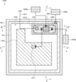
図1A~1Eは、光検出器又は画像感知デバイスを作製するために、光検出器のアレイを論理ウエハと共に含む画素ウエハなどの複数のウエハを使用する一般的な説明を提供する。図2~15Cに記載された実施形態の記載のコンテクスト及びコントラストを提供する説明を行う。 FIGS. 1A-1E provide a general illustration of using multiple wafers, such as a pixel wafer containing an array of photodetectors along with a logic wafer, to fabricate a photodetector or image sensing device. This illustration provides context and contrast for the description of the embodiments described in FIGS. 2-15C.
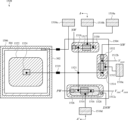
図1Aは、単一の画素ウエハ108上に形成された画素アレイ100を示す。画素アレイ100は、裏面106と反対側の上面102と共に示されている。画素104a及び104bなどの個々の画素は、単一光子アバランシェダイオード(SPAD)、及び場合によっては付随回路などの光受容体を含む。画素アレイは、様々な半導体製造プロセスのいずれかによって画素ウエハ108内に形成され得る。例えば、画素ウエハ108は、光受容体と、エッチング及び蒸着、イオン注入、及び/又は他の製造方法によって形成される任意の付随回路を有するp型半導体であってもよい。光受容体のアノード又はカソードへの付随回路構成要素又は接続構成要素は、裏面106が画像キャプチャのために光に露出した側であり得るように、製造プロセスによって上面102上に形成されてもよい。画素アレイ100は、相互接続パッド107.などの様々な相互接続パッドで作製され得る。
1A shows a
画素アレイ100は、本明細書では「論理ウエハ」と称される第2のウエハに結合され得るように作製され得、第2のウエハは、光受容体の電源電圧ライン又は接続のいずれか、光受容体の様々な制御トランジスタ(さらに後述されるような)、処理回路(例えば、バッファ、時間デジタルカウンタ、画像プロセッサ、フィルタなど)、又は他の構成要素を含み得る。
The
図1Bは、論理(又は制御回路)ウエハ112に接合又は結合された画素アレイ100の斜視図110を示す。画素ウエハ108は、裏面106が最上部に示されるように反転されており、ここで上面102が論理ウエハ112とインタフェース又は接合される。論理ウエハ112はまた、回路又は電気的接続をするように、画素アレイ100上に製作された相互接続パッド107と一致及び/又は接合する相互接続パッドを用いて製造される。
FIG. 1B shows a
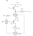
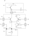
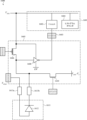
図1Cは、図1A~1Bに示されるような画像センサを形成しているデュアルウエハプロセスにおいて使用され得る回路120及び回路140の第1及び第2の回路図を示す。第2の回路140は、その内容全体が参照により本明細書に含まれる米国特許出願第15/879,350号の開示に基づく。回路120及び140では、光受容体は、それぞれの画素ウエハ、122及び142上に実装されたSPAD、124及び144であり、これらは図示の制御トランジスタ及び電圧源を含む論理ウエハに結合又は接合されている。
FIG. 1C shows first and second circuit diagrams of
第1の回路120において、高電圧VDDH134a、アノード電源電圧VSPAD134b、及びゼロ電圧源134c等の様々な電源電圧が存在し得る。SPAD124は、画素ウエハ122と論理ウエハとの間の相互接続パッド123aを介して、及び相互接続パッド123bを介して、アノード電源電圧VSPAD134bに電気的に連結される。
There may be various power supply voltages in the first circuit 120, such as a
本明細書において「論理回路」又は「制御回路」とも称される論理及び/又は制御回路は、少なくとも3つのトランジスタ:電圧VQを印加するpMOSクエンチングトランジスタ126、電圧VFRCHを印加するpMOS高速再充電トランジスタ128、及び電圧VGATEを印加するpMOSゲートトランジスタ、を含む。pMOSクエンチングトランジスタ126により、光子誘起アバランシェ電流の検出後に、SPAD124のバイアスをブレークダウン未満に減らすことが可能となる。pMOS高速再充電トランジスタ128は、SPAD124内の電荷キャリアの急速な復元を可能にするようにゲートされ得る。pMOSゲートトランジスタ130は、SPAD124からの出力シグナリングを制御することができる。出力信号は、レベルダウンシフタ(高電圧トランジスタ(単数又は複数)を有し得る)132a及びインバータ(場合によっては低電圧トランジスタ(単数又は複数)を有する)132bを介して送信され、そのいずれかはまた、出力接続リンク134dを介して後続の処理回路に増幅を提供し得る。当業者であれば、SPAD光受容体の第1の回路120の代替又は変形が可能であることを認識するであろう。
The logic and/or control circuit, also referred to herein as "logic circuit" or "control circuit", includes at least three transistors: a
第2の回路140は、そのような1つの変形を示す。第2の回路140では、SPAD144が画素ウエハ142に含まれている。第2の回路140は、第1の電源電圧152a及び第2の電源電圧152bを有する。画素ウエハ142は、相互接続パッド141a,141bを介して別個の論理ウエハ内の論理回路及び制御回路に、及びSPAD144のアノードに接続された第2の電源電圧152bに、電気的に接続され得る。第2の回路140は、電圧信号VRCHを印加するpMOS再充電トランジスタ148と、電圧信号VQCHを印加するpMOSクエンチングトランジスタ146と、電圧信号VGATEによって制御されるpMOS選択トランジスタ150a及びnMOSゲートトランジスタ150bの組み合わせと、を含む。nMOSゲートトランジスタ150bのソースは、回路グランドに接続されている。
A
図1Dは、画素ウエハ170が制御回路ウエハ112に接合又は結合され得る方法の一例の組み合わせ断面図及び回路図を示す。画素ウエハ170は、絶縁壁168などの絶縁壁によって分離されたSPAD画素162などのSPAD画素のアレイ100を含む。SPAD画素162は、アノード166及びカソード164を含む。画素ウエハ170はまた、制御回路ウエハ112へのビア174などのビア及び相互接続リンクを含む接合層172を含むことができる。画素ウエハ170は、インタフェース171に沿って制御回路ウエハ112と接合又は結合され得る。画素ウエハ170と制御回路ウエハ112との間の電気的接続は、相互接続パッド123a及び123bなどの相互接続パッドで提供されることができる。図示されるように、画素ウエハ170の上面は、図1A~1Bに関連して上述した裏面106であり得、ここで光感知又は画像キャプチャのために光に曝露される表面となっている。
1D shows a combined cross-sectional view and circuit diagram of one example of how the
制御回路ウエハ112は、1つ以上の電圧レベルを画素ウエハ170に提供することができ、また場合によっては上記の回路120及び140などのクエンチ/再充電回路182にも提供することができる電圧源180を含むことができる。
The
図1Eは、画素ウエハ170内のSPAD画素162のSPADなどのSPAD190の様々な詳細の断面図を示す。SPAD190は、p型アノード192及びn型カソード194が作製されたp型ボディ191を含む。p型アノード192とn型カソード194との接合部には、アバランシェ領域193が存在し得る。SPAD画素162は、絶縁壁168によって画素ウエハ170の隣接するSPADから電気的に遮蔽され得る。
1E shows a cross-sectional view of various details of a SPAD 190, such as the SPAD of a
SPAD画素162は、p型本体191がドーピング勾配を有するようにドープされ得、このドーピング勾配では、ドーパントの濃度は、勾配インジケータ196aによって示されるように、表面102から集光裏面106まで垂直方向と、勾配インジケータ196bによって示されるように、p型本体の中心から絶縁壁168まで横方向との両方向に増加する。SPAD画素162のドーピング勾配は、米国特許出願第15/713,477号、現在は米国特許第10,438,987号の開示に記載されるドーピング勾配に基づくことができ、その内容は参照によりその全体が本明細書に含まれる。
The
ドーピング勾配により、光子誘起電荷キャリアを、n型カソード194とp型アノード192との接合部へ誘導することが可能となり得る。例えば、中央到達光子198aは、次いで垂直勾配によって接合部へと誘導される電荷キャリア199a(この場合、電子)を生成することができる。あるいは、側壁付近のSPAD画素162に入射する光子198bは、横方向ドーピング勾配によって中心に向かって誘導され得る電荷キャリア199bを生成することができ、したがって、接合部でアバランシェ電流を誘導する可能性がより大きくなり得る。
The doping gradient may allow photon-induced charge carriers to be guided to the junction of the n-type cathode 194 and the p-
実施形態のファミリーの概要及び背景 Overview and background of the family of embodiments
以下に説明するのは、制御回路及び画素ウエハ、光受容体画素及びそれらに含まれるSPAD、並びに画像センサの一部を形成し得る他の構成要素の回路、構成、及びレイアウトの実施形態の少なくとも4つのファミリーである。この分類は限定的又は制限的であるとして解釈されるべきではないことを理解されたい。実施形態の様々な特徴、構成要素、及び構成は、2つ以上のファミリーで生じ得る。更に、これらのファミリーの実施形態に記載される特徴、構成要素、及び構成は、更に別の実施形態で組み合わされてもよい。 Described below are at least four families of circuit, configuration, and layout embodiments of control circuits and pixel wafers, photoreceptor pixels and their included SPADs, and other components that may form part of an image sensor. It is understood that this classification should not be construed as limiting or restrictive. Various features, components, and configurations of the embodiments may occur in more than one family. Additionally, features, components, and configurations described in embodiments of these families may be combined in yet other embodiments.
第1の実施形態について記載された特定の特徴、構成要素、及び下位構成要素の記載は、第2の実施形態の類似の特徴、構成要素、及び下位構成要素に関して参照されるか、又は適用されるものとして記載され得るが、第2の実施形態のそれらの類似の特徴、構成要素、及び下位構成要素は、それらの記載の範囲と一致する変形で実施され得ることを理解されたい。 Descriptions of certain features, components, and subcomponents described with respect to the first embodiment may be referenced or described as applying to analogous features, components, and subcomponents of the second embodiment, but it should be understood that those analogous features, components, and subcomponents of the second embodiment may be implemented in variations consistent with the scope of those descriptions.
これらの実施形態では、二重レベルの電源電圧:高レベルの電源電圧VDDH、及び低レベルの電源電圧VDDLが存在し得る。更に、実施形態は、SPAD電圧源及びグランド供給を有し得る。記載されたいくつかの実施形態では、特定の制御トランジスタ、例えばゲートトランジスタを画素アレイ上に配置することができる。いくつかの実施形態では、これらは、高電圧源で作動する必要があり得る制御トランジスタであってもよい。 In these embodiments, there may be a dual level power supply voltage: a high level power supply voltage V DDH and a low level power supply voltage V DDL . Additionally, the embodiments may have a SPAD voltage supply and a ground supply. In some embodiments described, certain control transistors, e.g. gating transistors, may be located on the pixel array. In some embodiments, these may be control transistors that may need to operate from a high voltage supply.
画素の様々な構成要素は、イオン注入、エッチング及び蒸着、又は他の製造技術などの様々な製造技術のいずれかによって形成されてもよい。様々な構成要素は、半導体ウエハ、例えば、p型基板又はn型基板に形成又は製造されてもよい。 The various components of the pixel may be formed by any of a variety of manufacturing techniques, such as ion implantation, etching and deposition, or other manufacturing techniques. The various components may be formed or fabricated in a semiconductor wafer, e.g., a p-type substrate or an n-type substrate.
第1のファミリー:SPAD画素セル内の2つのトランジスタ First family: two transistors in a SPAD pixel cell
実施形態の第1のファミリーは、光又は画像センサ、並びに論理又は制御回路ウエハに接合又は結合された画素ウエハ上に形成された画素のアレイを含む、それらの内部構成要素及び特徴を対象とする。画素は、光検出器としてSPADを含むことができる。実施形態の第1のファミリーでは、制御回路のトランジスタのうちの2つが、画素毎に画素ウエハ上に形成されている。画素は、本明細書では、「画素セル」とも称される。 The first family of embodiments is directed to light or image sensors and their internal components and features, including an array of pixels formed on a pixel wafer bonded or coupled to a logic or control circuit wafer. The pixels may include a SPAD as a photodetector. In the first family of embodiments, two of the transistors of the control circuit are formed on the pixel wafer for each pixel. The pixels are also referred to herein as "pixel cells."
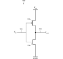
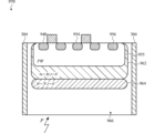
図2は、画素セル210及び関連する制御及び供給回路の一実施形態の一般化された図200を示す。画素セル210は、画素ウエハ上の画素アレイの部分であってもよい。画素セル210は、一般に、SPAD、ゲートトランジスタ、クエンチングトランジスタなどの高電圧回路素子を含んでいる。画素セル210は、上述したように、別個の制御ウエハ上に配置され得る外部回路構成要素との電気的接続を提供する、相互接続パッド212a~212dを有する。相互接続パッド212a~212dは、銅であり得、論理ウエハ上の一致する銅の相互接続パッドと接合され得る。
Figure 2 shows a generalized diagram 200 of one embodiment of a
対照的に、低電圧回路セグメント224は、クエンチングトランジスタ、バッファ/インバータなどの低電圧素子を含んでいる。一般に、低電圧回路セグメント224は、画素セル210の外部の回路を含み、VDDLソース202から電圧を引き出すことができる。出力信号は、接続208を介して、信号調整及び画像処理構成要素などの更なる構成要素に送信されてもよい。
In contrast, the low voltage circuit segment 224 includes low voltage elements such as quenching transistors, buffers/inverters, etc. In general, the low voltage circuit segment 224 includes circuitry external to the
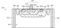
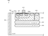
図3Aは、画素セル210の構成要素の第1の構成を提供する画素セル300の平面図を示す。図示された画素セル300の表面は、図1Aの表面102に対応することができ、画素セル300の集光面は、画素セル300の図示された表面とは反対側にある。画素セル300は、画素セル300を画素ウエハ内の他の画素セルから分離した絶縁層302でリングされた長方形のウェルで構成されている。絶縁層は、二酸化ケイ素であり得る。画素セル300は、絶縁層302に内部的に隣接するアノード層304を有している。アノード層304は、p型であり得、相互接続パッド212dに電気的に接続され得る。
FIG. 3A shows a plan view of a
画素セル300は、アノード層304の内部に浅いトレンチ分離(STI)層306を備え、少なくとも3つの領域:分離されたウェル内にある、第1のトランジスタ領域315a、中央のSPAD領域315b、及び第2のトランジスタ領域315c、を形成しているように構成されている。示された実施形態の特定のバージョンでは、第1のトランジスタ領域315aは、中央SPAD領域315bの第1の側に配置されており、第2のトランジスタ領域315cは、第1の側とは反対側の中央SPAD領域315bの第2の側に配置されている。示された実施形態の特定のバージョンでは、STI層306は、第1のトランジスタ領域315a、中央SPAD領域315b、及び第2のトランジスタ領域315cの周りに周囲リングを形成している。本実施形態の他の変形例は、3つの領域の代替的な配置を有し得る。
The
この構成のSPAD214は、以下に更に図示及び記載されるように、(図示の配向に対して)p型アノード層の上に配置されたn型カソード層320として実装され得る。SPAD214は、n型カソード層320に接続されたカソード電極322を有し得る。カソード電極は、n型カソード層の一部又は全部の上に延在していることができる。カソード電極322は、金属又は他のトレースであり得る相互接続線324と電気的に接続され得る。
The
(図2の画素セル210の一部であり得る)pMOS HVクエンチングトランジスタは、第1のトランジスタ領域315a内に位置し得る。pMOS HVクエンチングトランジスタ216は、n型半導体ウェル(NW)310a内に位置し得る。NW310aは、NW接続線310cにリンクされた、NWバイアス区分310bを有し得る。バイアス電圧は、NW接続線310cに印加することができる。いくつかの変形例では、バイアス電圧は0.8Vであり得、他のバイアス電圧を使用することもできる。pMOS HVクエンチングトランジスタ216のソースは、上述のように、相互接続パッド212aに接続されている。pMOS HVクエンチングトランジスタ216のドレインは、相互接続線324と連結されて、画素セル210内にノード220を形成している。pMOS HVクエンチングトランジスタ216のゲート217は、上述のように、相互接続パッド212bと連結されている。
The pMOS HV quenching transistor (which may be part of the
nMOSゲートトランジスタ218は、第2のトランジスタ領域315c内に位置し得る。nMOSゲートトランジスタ218は、p型半導体ウェル(PW)344内に位置し得る。PW344は、PWバイアス電圧が印加され得るPW接続リンク346bと連結されたPWバイアス区分346aを有することができる。いくつかの変形例では、PWバイアス印加電圧はVDDL~VDDHであり得る。次いで、PW344は、深いn型半導体ウェル(DNW)340内に位置する。DNW340は、DNW接続線342bに連結されたDNWバイアス区分342aを有し得る。バイアス電圧は、NW接続線310cに印加することができる。いくつかの変形例では、バイアス電圧は0.8Vであり得、他のバイアス電圧を使用することもできる。上記のように、nMOSゲートトランジスタ218のソースは、電圧供給リンク222に沿って電源電圧VDDL~VDDHに接続されている。nMOSゲートトランジスタ218のドレインは、相互接続線324と連結されて、ノード220を形成している。nMOSゲートトランジスタ218のゲート219は、上述したように、相互接続パッド212cと連結されている。
The nMOS
相互接続パッド212a~212dは、図示の上面の平面内ではなく、画素セル300の表面の上方に(すなわち、ページの外に)位置付けられ得る。相互接続パッド212a~212dのそのような構成又は位置決めは、図1Dに基づくことができる。このような構成、又は同様の構成により、画素セル300を収容するウエハは、図2に示す外部回路構成要素(例えば、高電圧回路セグメント224)を含む制御ウエハに接合されることが可能となる。
The
図3Bは、図3Aの水平切断線A-A’に沿った水平(「X軸」)断面図350を示す。断面図350の左縁部及び右縁部は、絶縁層302及びアノード層304が、イメージングで受光される裏面106まで延在し得ることを示しているが、これは必須ではない。断面図350は、画素セル300がp型基板354(P-EPI)を含み、その中にpMOS HVクエンチングトランジスタ216が形成されていることを示す。STI層306は、裏面106まで延在していることなく形成され得るが、pMOS HVクエンチングトランジスタ216を電気的に絶縁するのに十分に延在してもよく、NW310aよりも深く延在してもよいが、これは必須ではない。NW310aは、STI層306に接触するように延在し得るか、又は、NW310aとSTI層306との間のp型基板354の延長部を含む間隙が存在し得る。断面図350に示される実施形態の特定のバージョンでは、NWバイアス区分310bは、ドレイン352a及びpMOS HVクエンチングトランジスタ216のソース352bから離れて配置されている。
3B shows a horizontal ("X-axis") cross-section 350 taken along horizontal cut line A-A' in FIG. 3A. The left and right edges of cross-section 350 show that the insulating
図3Cは、図3Aの水平切断線B-B’に沿った画素セル300の水平(「X軸」)断面図360を示す。絶縁層302のアノード層304及びSTI層306は、図3Bに関して説明したとおりであり得る。この実施形態の画素セル300は、p型アノード層362の上方に配置されたn型カソード層320を有する。STI層306は、p型アノード層362よりも深く延在し得るが、これは必須ではない。p型基板354は、図1Eに関してなされた説明に基づき得るドーピング勾配輪郭レベル364a及び364bと共に示されている。n型カソード層320は、上述のように、ノード220に電気的接続を提供するカソード電極322を有する。
Figure 3C shows a horizontal ("X-axis")
図3Dは、図3Aの水平切断線C-C’に沿った画素セル300の水平(「X軸」)断面図370を示す。絶縁層302、アノード層304及びSTI層306は、図3Bに関して説明したとおりであり得る。PW344は、DNW340に含まれていることが示されている。PWバイアス区分346aは、DNWバイアス区分342aの位置と対向するnMOSゲートトランジスタ218の側のPW344内に配置されているが、これは必須ではない。上記のように、nMOSゲートトランジスタ218のドレイン343a及びソース343bを通る導通は、ゲート219に印加される電圧信号によって制御される。
Figure 3D shows a horizontal ("X-axis") cross-section 370 of
図3Eは、図3Aの垂直切断線D-D’に沿った画素セル300の垂直(「y軸」)断面図380を示す。断面図380は、勾配レベル線386a及び386bによって示されるp型基板354内のドーピング勾配が、pMOS HVクエンチングトランジスタ216及びnMOSゲートトランジスタ218の下に延在し得ることを示す。このようなドーピング勾配により、画素セル300の裏面の中心で受容した光子によって誘起される光子誘起電荷キャリア388aは、偏向することなくp型アノード層362とn型カソード層320との境界面のアバランシェ接合領域に向かって導かれ得る。しかし、画素セル300の裏面の縁部に向かって受容される光子は、ドーピング勾配により、アバランシェ接合領域に向かって偏向され得る。
Figure 3E shows a vertical ("y-axis")
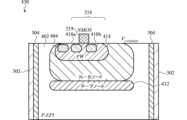
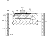
図4Aは、2つの制御トランジスタが画素ウエハの各画素セルに含まれ得る、第2の実施形態の平面図を示す。画素セル400は、図2に関して説明した回路を実装することができる。画素セル400は、図3に関連して説明及び示された、pMOS HVクエンチングトランジスタ216及びnMOSゲートトランジスタ218のレイアウト又は構成を実装する。図3A~3Eに記載されている実施形態とは異なり、画素セル400は、構成要素のための分離された領域を形成している浅いトレンチ分離を使用しない。その代わりに、画素セル400は、アバランシェ接合部を形成しているn型カソード層とp型アノード層の両方が画素セル400の表面の下に少なくとも部分的に形成されるSPADを実装する。
Figure 4A shows a plan view of a second embodiment in which two control transistors may be included in each pixel cell of a pixel wafer. The
図4Aは、図3A~3Eに関連して上述したように、周囲の絶縁層302及びアノード層304を有する長方形ウェルとして形成された画素セル400を示す。アノード層304は、前述のように、相互接続パッド212dを介してバイアス電圧ソースVSPADに電気的に接続され得る。画素セル400の構成要素は、図4B~4Cにより詳細に示されるように、p型基板402内又は上に形成され得る。p型基板402内で、ノード220への電気的接続としてカソード電極420を有するn型ウェル(NW)404内に形成され得る。
Figure 4A shows a
図4Aに示す構成では、pMOS HVクエンチングトランジスタ216は、内部NW408内に配置され得、それ自体は深いp型ウェル(DPW)406内に配置されている。DPWには、DPWバイアス区分412にバイアス電源電圧が設けられてもよく、内部NW408は、NWバイアス区分411bに設けられたNWバイアス電圧411aと連結されてもよい。図3A~3Eの実施形態について説明したように、pMOS HVクエンチングトランジスタ216は、相互接続パッド212aに接続されたソースと、相互接続パッド212bに接続されたそのゲート217と、ノード220に接続されたそのドレインとを有することができる。
In the configuration shown in FIG. 4A, the pMOS
nMOSゲートトランジスタ218は、PWバイアス電圧419bによってバイアス区分419aに供給され得るPW414内に配置されてもよい。nMOSゲートトランジスタ218は、図3A~3Eの実施形態について説明したように接続されたドレイン及びソースと、相互接続パッド212cに接続されたそのゲート219とを有することができる。pMOS HVクエンチングトランジスタ216は、そのソース/ゲート/ドレイン軸が、nMOSゲートトランジスタ218のソース/ゲート/ドレイン軸に直角となって示されているが、これは必須ではない。
The nMOS
図4Bは、nMOSゲートトランジスタ218を通る、図4Aの切断線B-B’に沿った画素セル400の水平断面(「X軸」)図430を示す。図430は、画素セル400のSPADのカソードを形成しているn型カソード層404内のPW414の配置を示す。p型アノード層432は、p型基板402内でn型カソード層404の下に埋設層として配置されている。nMOSゲートトランジスタは、ゲート219に関して示されるように、PW414内に配置されたそのドレイン418aと、ソース418bとを有する。
Figure 4B shows a horizontal cross-sectional ("X-axis") view 430 of
図4Cは、図4Aに示される二重及びシフトされた切断線A-A’及びC-C’に沿った、シフトされた(「ジグザグ」)垂直断面図(「y軸」)440を示す。図4Cは、n型カソード層404が、pMOS HVクエンチングトランジスタ216及びnMOSゲートトランジスタ218の下の埋設層として延在してもよく、また、それぞれ、pMOS HVクエンチングトランジスタ216及びnMOSゲートトランジスタ218の絶縁を提供するDPW416及びPW414から離れて画素セル400の表面に延在し得ることを示す。前述したように、p型基板402は、光子誘導電荷キャリアを画素セル400の中心に導くように動作し得るドーピング勾配輪郭線444a及び444bによって示されるような、ドーピング勾配を有し得る。
Figure 4C shows a shifted ("zig-zag") vertical cross-section ("y-axis") 440 along the double and shifted cut lines A-A' and C-C' shown in Figure 4A. Figure 4C shows that the n-
図5Aは、特定の詳細部を有するが、図2の回路図200と概念的に類似している回路図500を示す。回路図500では、図3のnMOSゲートトランジスタ218の代わりに、pMOSゲートトランジスタ518が使用されている。図5Aに示される他の構成要素は、図2及び3に関連して説明されたとおりである。
FIG. 5A shows a circuit diagram 500 that is conceptually similar to the circuit diagram 200 of FIG. 2, but with certain details. In circuit diagram 500, a pMOS
図5Bは、2つの制御トランジスタが画素ウエハの各画素に含まれ得る第3の実施形態の構成の平面図を示す。画素510は、図3A~3Eに関連して説明される画素セル300と類似している。具体的には、画素510は、STI層306を使用して、図5Aに示す構成要素の分離領域を形成している。領域512は、画素セル300について説明したとおりであり得る。画素510は、画素セル300のnMOSゲートトランジスタ218の代わりにpMOSゲートトランジスタ518が存在するという点で、画素セル300とは異なる。pMOSゲートトランジスタ518は、図示のように、相互接続パッド212cに接続されたゲート519を有する、NW516内に形成される。NW516は、NWバイアス電圧514bが印加されるバイアス区分514aを有し得る。図5Bの水平切断線C-C’に沿って、断面図は、図3Bに示される断面図と類似しており、同様の対応する記載を含んでいる。
Figure 5B shows a plan view of a third embodiment configuration in which two control transistors may be included in each pixel of a pixel wafer.
図6Aは、SPAD614及び2つの制御トランジスタ、並びに関連する供給及び制御回路要素を含むSPAD画素セルを示す回路図600である。これは、SPAD光検出器のアレイを有する画素ウエハは、そうでなければ画素ウエハが接合又は結合される論理ウエハ上に配置され得る、2つの制御トランジスタを含むことができる、第4の実施形態を示す。図6Aの実施形態は、各画素セル602内に2つのnMOSトランジスタを含み、そのため、バイアスは、前述の実施形態とは異なる方式で実装され得る。
Figure 6A is a circuit diagram 600 showing a SPAD pixel cell including a
画素セル602の外部にある関連する供給及び制御回路要素は、そのソースが回路グランド606に接続されており。そのドレインが画素セル602の相互接続パッド612dにリンクされたnMOSクエンチングトランジスタ604を含み得る。nMOSクエンチングトランジスタ604は、ゲート605に印加された電圧信号VBNなどのゲート605で受信された信号によって制御される。画素セル602の出力は、nMOSクエンチングトランジスタ604のドレインで受信され、バッファ608によって送信され、バッファ608はまた、出力ライン609上に信号の増幅も与え得る。
Associated supplies and control circuitry external to the
画素セル602は、少なくともSPAD614、nMOSバイアストランジスタ616、及びnMOSゲートトランジスタ618を含む。nMOSバイアストランジスタ616は、光子検出のためにSPAD614を逆バイアス状態にするように動作することができる。nMOSゲートトランジスタ618のドレインはVDDHでバイアスされ、そのゲートは、相互接続パッド612bを介してゲート信号を受信するように連結されている。SPAD614のカソードは、相互接続パッド612aを介して電源電圧VSPADに接続することができる、この電源電圧VSPADは、この実施形態のいくつかの実装では、VSPAD=VBD+VDDHであり得、VBDはSPAD614のブレークダウン電圧である。
The
図6Bは、画素セル602内の回路図600の回路構成要素のレイアウト又は構成の平面図610を示す。先の実施形態について説明したように、画素セル602は、内部がアノード層304となっている長方形の絶縁層302内に収容され得る。画素セル602内の構成要素は、p型基板622上に実装され得る。n型カソード層624は、以下に示すように、nMOSバイアストランジスタ616及びnMOSゲートトランジスタ618の下に延在しているように埋設層内に存在することができ、大きなアバランシェ接合領域を提供する。n型カソード層はまた、以下に示すように、上面まで延在していることができ、相互接続パッド612aに接続されたカソード電極620を有する。
Figure 6B shows a
nMOSバイアストランジスタ616及びnMOSゲートトランジスタ618は、それぞれ、PW613及び617内に形成されている。PW613及び617は、簡略化のために示されていないが、バイアス区分419aに類似したバイアス区分を有することができ、バイアス区分419aにおいてそれぞれのバイアス電圧が印加され得る。nMOSバイアストランジスタ616及びnMOSゲートトランジスタ618は、ドレイン/ゲート/ソース軸が直交するように配置されているが、この実施形態の他の変形例では、nMOSバイアストランジスタ616及びnMOSゲートトランジスタ618は、画素セル602内では異なって配置されてもよい。nMOSバイアストランジスタ616のゲート615は、相互接続パッド612cと連結され、nMOSゲートトランジスタ618のゲート619は、相互接続パッド612bと連結されている。
The
図6Cは、図6Bに示す切断線B-B’に沿った水平断面図630を示す。nMOSゲートトランジスタ618は、PW617内に形成されている。PW617自体は、n型カソード層624内に形成され、これは、PW617の下及びそれを超えて延在し得る。p-アノード層632は、n型カソード層624の下に形成されて、p-アノード層632とn型カソード層624との接合部における大きなアバランシェ領域を可能にする。p型基板622は、前述したように、ドーピング勾配で実装され得る。図6Cもまた、図6Bの切断線A-A’に沿った垂直断面図を示しているため、説明は繰り返さない。
Figure 6C shows a
図7Aは、画素ウエハの各画素セルに2つの制御トランジスタが含まれた、第5の実施形態の画素セル700の構成の平面図を示す。この構成は、図6Aの画素セル602に関連して説明された回路素子に基づくものである。この違いは、ここでは、画素セル700はn型基板上に形成され、制御トランジスタは、nMOSであり、それぞれの深いn-ウェル(DNWs)に形成されていることである。
Figure 7A shows a plan view of a
先の実施形態について説明したように、画素セル700は、長方形の絶縁層302内に収容され得る。しかしながら、ここでは、絶縁層302に内部で隣接するn型カソード層705が存在する。この実施形態では、n型カソード層705は、相互接続パッド612aを介してカソード電圧VSPADにバイアスをかけるカソードに連結されている。VSPADは、VSPAD=VBD+VDDH、VBDについてはブレークダウン電圧として設定され得るが、これは必須ではない。
As described in the previous embodiment, the
画素セル700は、以下に更に示すように、nMOSバイアストランジスタ616及びnMOSゲートトランジスタ618の下に延在し、n型基板に形成されたn型カソード層の上方に配置されたp型アノード層704を含むことができる。p型アノード層704はアノード電極720と接続する。
The
nMOSゲートトランジスタ618は、相互接続パッド612bを介して画素セル700の外部の制御回路に連結されたゲート716に印加される信号によって制御される。nMOSゲートトランジスタ618は、PW714内に配置されている。PW714は、バイアス電圧が印加されるバイアス区分719を有してもよい。PW714は、DNW712内に形成され、これは、DNWバイアス電圧が印加されるバイアス区分717を有し得る。ゲート716は、相互接続パッド612bに接続し、そこから外部信号を受信する。nMOSゲートトランジスタ618のソースは、VDDHであり得るVDDHソースに接続することができる。
The
nMOSバイアストランジスタ616は、nMOSゲートトランジスタ618と同様に構成又は形成されてもよい。nMOSバイアストランジスタ616は、DNW706内に形成され得るPW708内に形成されてもよい。PW708及びDNW706は、上述のようにそれぞれのバイアス区分で実装され得るが、簡潔にするために図示されていない。nMOSバイアストランジスタ616のゲート710は、相互接続パッド612cに連結され、相互接続パッド612cを介して外部信号を受信することができる。nMOSバイアストランジスタ616のドレインは、一般に、nMOSゲートトランジスタ618のドレインと共に相互接続パッド612dを介して、外部回路構成要素に連結されている。
The
図7Bは、図7Aの切断線A-A’に沿った水平断面図730を示す。nMOSゲートトランジスタ618は、PW714の断面図に示されており、これは次にDNW712内にある。DNW712の下に延在しているp-アノード層732の一部が存在し、これはまた、画素セル700の上面に延在している延長部704を有し得る。n型カソード層734は、p-アノード層732の全て又は大部分の下に形成されて、n型カソード層734及びp-アノード層732によって形成されるアバランシェ領域のサイズを増大させることができる。n型カソード層734の下のn型基板702の領域は、ドーピング勾配輪郭レベル738aび738bによって示されるように、ドーピング勾配で形成され得る。
Figure 7B shows a
図7A~7Bに関連して説明された第5の実施形態と同様に、図6A~6Cに関連して説明される第4の実施形態を実装するが、半導体の原子価タイプ(n型及びp型)が基板に対して反転されており、SPADのアノード及びカソードに関しては、当業者であれば、他の前述の実施形態を同様に逆の半導体タイプで実装する方法を理解するであろう。同様に、以下の実施形態のそれぞれに関して、同様に反転された半導体タイプを有する類似の対応する実施形態が存在することが理解されるであろう。 Similar to the fifth embodiment described in connection with Figures 7A-7B, the fourth embodiment described in connection with Figures 6A-6C is implemented, but with the semiconductor valence types (n-type and p-type) reversed with respect to the substrate, with respect to the anode and cathode of the SPAD, and one of ordinary skill in the art would understand how to similarly implement the other aforementioned embodiments with reversed semiconductor types. Similarly, it will be understood that for each of the following embodiments, there are similar corresponding embodiments having similarly reversed semiconductor types.
第2のファミリー:SPAD画素セル内の少なくとも3つのトランジスタ Second family: at least three transistors in a SPAD pixel cell
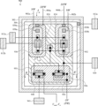
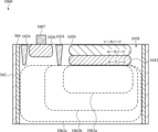
このセクションの以下の実施形態では、SPAD画素のアレイを含む画素ウエハが、各画素セル内に3つの制御トランジスタを含み得る回路及び構成を説明する。そのような制御トランジスタは、他の実装形態では、画素ウエハが接合される論理ウエハ上に配置され得る。画素ウエハ上に3つの制御トランジスタを含むことにより、論理ウエハ上の回路構成要素により多くのスペースを提供することができる。これらの実施形態で説明される回路及び構成は、各SPAD内で大きなアバランシェ領域を維持することができる。以下の実施形態の特徴、構成要素、及び下位構成要素の多くは、前述の実施形態の特徴、構成要素、及び下位構成要素と類似又は類似し得るため、そのような特徴、構成要素、及び下位構成要素は、同じ詳細には記載されない。当業者であれば、有用であるか又は必要であり得るような、可能な変形及び適応を認識するであろう。 The following embodiments in this section describe circuits and configurations in which a pixel wafer containing an array of SPAD pixels may include three control transistors in each pixel cell. Such control transistors may be located on a logic wafer to which the pixel wafer is bonded in other implementations. Including three control transistors on the pixel wafer may provide more space for circuit components on the logic wafer. The circuits and configurations described in these embodiments may maintain a large avalanche area within each SPAD. Many of the features, components, and subcomponents of the following embodiments may be similar or similar to the features, components, and subcomponents of the previous embodiments, and therefore such features, components, and subcomponents will not be described in the same detail. Those skilled in the art will recognize possible variations and adaptations that may be useful or necessary.
図8Aは、画素セル802内に3つのトランジスタが存在する第6の実施形態の回路図800である。画素セル802及びSPAD810は、そのアノードで、電圧ソースVSPADへの相互接続パッド812eに接続されている。SPAD810のカソードは、高電圧クエンチングトランジスタである、第1の内部pMOSトランジスタ814のドレインに接続されており。そのゲート815は、制御信号が受信され得る相互接続パッド812bに接続されている。第1の内部pMOSトランジスタ814のソースは、相互接続パッド812aに接続されており。それを介して電源電圧VDDL805が受信される。外部pMOSトランジスタ804は、低電圧クエンチングトランジスタである。外部制御回路は、相互接続808上のSPADの出力信号を論理又は制御ウエハの更なる構成要素に適用する反転バッファ806を含むことができる。
8A is a circuit diagram 800 of a sixth embodiment in which there are three transistors in the
画素セル802は、pMOS再充電トランジスタ818を含んでおり、そのゲート817は相互接続パッド812cに接続されており。それを介して更なる制御信号が印加され得る。pMOS再充電トランジスタ818は、VDDHレベルの電源電圧よってそのソースに供給される。これらの実施形態では、提供される2つの高電圧:VDDL及びVDDH、並びにそのオフセット及びアノード電圧VSPADが存在する。pMOS再充電トランジスタ818のドレインは、相互接続パッド812dに接続されたゲート821を有するnMOSゲートトランジスタ820のドレインと直列に接続されており。相互接続パッド812dを介してゲート信号(例えば、「オン/オフ」信号)は、外部制御回路から受信され得る。pMOS再充電トランジスタ818及びnMOSゲートトランジスタ820のドレインを接続しているノードは、SPAD810のカソードに接続する。nMOSゲートトランジスタ820のソースは、低くした電源電圧822に接続されており、この電圧はVDDL~VDDHの値、又は別の値を有し得る。
The
図8Bは、図8Aの画素セル802の特定素子の構成の平面図830を示す。画素セル802は、前述のように、その内部では境界アノード層304である絶縁層302によって囲まれている。画素セル802は、それぞれp型及びn型であり得る半導体基板832内に形成されたn型カソード層834を有する。カソード電極824は、n型カソード層834の表面に形成され得る。正方形として示されているが、カソード電極824は、多かれ少なかれカソード電極824の上に延在してもよい。
Figure 8B shows a
第1の内部pMOSトランジスタ814及びpMOS再充電トランジスタ818の両方は、それぞれのNW838a及び838b内に形成され、これは次に、それぞれの深いp-ウェル(DPWs)836a及び836b内に形成されている。第1の内部pMOSトランジスタ814及びpMOS再充電トランジスタ818は、それらのソース/ゲート/ドレイン軸と並列に配置されているが、他の配置及び構成が使用されてもよい。nMOSゲートトランジスタ820は、PW823内に形成されている。
Both the first
図8Cは、切断線A-A’に沿った、図8Bに関連して説明される構成を有する画素セル802の断面図840を示す。n型層842は、n型カソード層の一部であってもよく、SPAD810のカソードの一部を形成している。図示のように、SPAD810のp型アノード層844は、n型層842の下の半導体基板832内に形成されている。n型層842は、図示のように、DNW836a及び836bの下に延在して、n型層842及びp型アノード層844の境界面におけるアバランシェ接合領域を増加させることができる。DNW836a及び836bから離れて、n型層842は、画素セル802の上面に近接して延在し得るn型カソード層842に接合する。
Figure 8C shows a
図8Dは、切断線B-B’に沿って図8Bに関連して説明される構成を有する画素セル802の断面図850を示す。nMOSゲートトランジスタ820は、n型カソード層834内に順に形成される、PW823内に形成されて示されている。p型アノード層844は、n型カソード層834の下に延在している。n型カソード層834及びn型カソード層834の下のp型アノード層844の拡張は、それらの境界面でのアバランシェ接合領域の増加を提供する。
Figure 8D shows a
図9Aは、図8A~8Dに関連して説明された実施形態の第1の変形例の平面図900を示す。図9Aに示される実施形態は、図8Aに示す回路図800を修正して、nMOSゲートトランジスタ820を、ゲート921を有するpMOSゲートトランジスタ920に置き換える。回路図800の他の構成要素は、説明されたとおりである。平面図900は、上記の平面図830について説明した通りであるが、ただし、pMOSゲートトランジスタ920は、NW912内に形成され、これは次に、DPW910内に形成されている。制御トランジスタにpMOSのみを使用することにより、本実施形態のより単純な製造が可能となり得る。図9Aの切断線B-B’に沿った断面図は、図8Cの断面図と類似している。
Figure 9A shows a
図9B~9Eは、図8A~8Dに関連して説明された実施形態の第2の変形例を示す。この第2の変形例では、インバータ806の構成トランジスタは、ゲートトランジスタ及び再充電トランジスタと共に、SPADを含む画素セルの一方の側に配置される。そのような実施形態は、画素セル上に実装されるインバータが高電圧トランジスタを使用するのに対して論理回路ウエハ上に配置されたインバータは低電圧トランジスタで実装され得るため、速度の改善が可能となり、したがって画素セル802の出力間の電圧レベルシフタの必要性がなくなる。図9B~9Eの実施形態において、画素セルのSPADは、以下に記載されるように、SPAD接合部用の大部分が埋められたアノード及びカソードで形成され、トランジスタは画素ウエハのフロント側で形成されている。SPADのカソードは、フロント側を通って延在し得、例えば、その上のトランジスタへの電気的接続を行う。
9B-9E show a second variation of the embodiment described in connection with FIGS. 8A-8D. In this second variation, the constituent transistors of the
図9Bは、画素ウエハの画素セル932が、SPAD934、インバータ938、pMOS再充電トランジスタ936、及びnMOSゲートトランジスタ940を含む構成930を示す。画素セル932は、電圧供給線VDDL931と、接点933を介して供給された電圧VSPADとによって供給される。画素セル932を含む画素ウエハは、論理回路ウエハ945と接合又は結合されてもよい。再充電トランジスタ936のゲートは、接点937を介して印加される信号によって制御され、ゲートトランジスタ940のゲートは、接点941を介して印加される信号によって制御される。
9B shows a
図9Bはまた、金属-金属接続部939を介して画素セル932に接続され得る論理回路ウエハ945の区分を示す。代替的に、論理回路ウエハ945は、図15Cに関連して以下に記載されるように、貫通シリコンビア(TSV)によって、画素セル932を含む画素ウエハと接合又は接続され得る。論理回路ウエハ945は、画素セル932の出力に基づいて標準パルスを生成する1ショット942を含むことができる。次いで、1ショットの出力は、ヒストグラムカウンタ944によって受信され得る。論理回路ウエハ945は、ヒストグラムカウンタのデータを使用して画像情報又は他の情報を生成し得る、マイクロコントローラ、マイクロプロセッサ、信号プロセッサ、メモリ、又は他の構成要素を含むことができる。
9B also shows a section of
図9Cは、インバータ938を実装するために使用され得る2つのトランジスタの構成950を示す。上部pMOSトランジスタ952は、そのドレインが下部nMOSトランジスタ954のソースと接続するように積層されている。上部pMOSトランジスタ952のソースは、電圧VDDによって供給され、下部nMOSトランジスタ954のドレインはグランドに接続されている。入力信号VIN951が、図示された両方のトランジスタのゲートに印加されると、出力信号VOUT953は、入力信号VIN951に対して極性が反転される。画素セル932内のインバータ938のこの実装を使用すると、2つのnMOSトランジスタ、ゲートトランジスタ940及びインバータ938の下部nMOSトランジスタ、並びに2つのpMOSトランジスタ:再充電トランジスタ936及びインバータ938の上部pMOSトランジスタが存在する。
9C shows a two
図9Dは、画素セル932のフロント側(集光裏面の反対側)に実装された、ゲートトランジスタ940、再充電トランジスタ936、上部pMOSトランジスタ952、及び下部nMOSトランジスタ954の構成960を示す。この構成は、図8B及び9Aに示された構成の変形である。図8B及び9Aにも示され、図9Dに示される特徴は、上記のとおりであり得る。pMOSトランジスタ936及び952は、それぞれ、分離されたn型ウェル(NW)838a及び838bに形成されている。次に、2つのNW838a及び838bは、深いp型ウェル(DPW)836a及び836b内に形成されている。この実施形態では、DPWは単一のDPWとして形成され得るが、これは必須ではない。
Figure 9D shows a
図9Dの構成では、2つのnMOSトランジスタ940及び954は、共通のp型ウェル(PW)955内に形成されている。PW955は、接続パッド956などの1つ以上の場所でグランド(0V)にバイアスされ得る。インバータ938の出力は、金属-金属接続、又は別の種類であり得る接続939を介して論理回路ウエハ945に接続されてもよい。
In the configuration of FIG. 9D, two
図9Dの示された切断線A-A’に沿った断面図は、図8Cの対応する特徴について示されているとおりであり、説明は繰り返さない。 The cross-sectional view along the indicated section line A-A' in FIG. 9D is as shown for the corresponding features in FIG. 8C and will not be repeated.
図9Eは、図9Dの切断線B-B’に沿った断面図970を示す。図9Eは、SPAD934の接合部を形成しているn型カソード962及びp型アノード964の区分が、インバータ938、pMOS再充電トランジスタ936、及びnMOSゲートトランジスタ940の4つのトランジスタを形成している半導体構造の下に形成されていることを示す。n型カソード962及びp型アノード964は、図1Eに関して上述したように、p型本体966内に形成され得、これはドーピング勾配によって実装され得る。n型カソード962の区分は、カソード電極824(などのフロント側(図9Eの上部に示される)まで延在してもよい。
9E shows a
第3のファミリー:SPAD画素セル内の単一トランジスタ Third family: single transistor in SPAD pixel cell
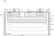
このファミリーの実施形態では、画素セルは、SPAD及び単一の制御トランジスタで形成されている。これらの実施形態は、対応する画素アレイの製作を容易にすることができる。例えば、実施形態は、関連する制御回路ウエハと接合する相互接続パッドをより少なくすることができる。 In embodiments of this family, the pixel cell is formed with a SPAD and a single control transistor. These embodiments can facilitate fabrication of the corresponding pixel array. For example, the embodiments can require fewer interconnect pads to bond with the associated control circuit wafer.
図10Aは、画素セル1002の画素アレイ区分、及び関連する外部制御回路を有する回路図1000である。画素セル1002は、SPAD1004及びpMOS高電圧(HV)クエンチングトランジスタ1006を含んでいる。前述のように、制御回路は、画素セル1002を含む画素ウエハに接合された別個のウエハ上に配置され得る。制御回路は、そのソースが電圧ソース1014に接続された低電圧クエンチングトランジスタ1010を含み、この電圧ソース1014は、レベルVDDLであり得る。低電圧クエンチングトランジスタ1010のドレインは、相互接続パッド1008aにおいて画素セル1002に接続し、相互接続パッドを介して画素セル1002からの信号が取得される。画素セル1002からの信号は、反転バッファ1012によって調整(例えば、増幅又は緩衝)されて、更なる論理回路に送信され得るVOUTを生成することができる。
10A is a circuit diagram 1000 having a pixel array section of a
SPAD1004のアノードは、バイアス電圧VSPADが印加される相互接続パッド1008cに接続されている。SPAD1004のカソードは、そのゲート1007において相互接続パッド1008bを介して制御信号を受信する、pMOS HVクエンチングトランジスタ1006のドレインに接続している。
The anode of
図10Bは、図10Aの回路図を実装する構成における画素セル1002の上面の平面図1020を示す。pMOS HVクエンチングトランジスタ1006は、SPAD1004内のアバランシェ領域を増大できるように、画素セル1002のコーナーに配置されている。画素セル1002は、前述の実施形態に記載されているように、周囲の絶縁層302及びその境界アノード層304で形成され得る。画素セル1002は、p型半導体基板1028内に形成されたn型カソード層1030を含むことができる。n型カソード層1030は、pMOS HVクエンチングトランジスタ1006のドレインに接続されたカソード電極1032を有することができる。pMOS HVクエンチングトランジスタ1006は、浅いトレンチ分離(STI)ウェル1024によって、n型カソード層1030から分離され得る。STIウェル1024内で、pMOS HVクエンチングトランジスタ1006は、NW1026内に形成されている。NW1026は、先の実施形態で説明したように、電圧ソースによって供給されるバイアス区分(簡潔にするために図示されていない)を有し得る。
10B shows a
図10Cは、図10Bの切断線B-B’に沿った画素セル1002の断面図1040である。pMOS HVクエンチングトランジスタ1006は、NW1026内に形成されSTI壁1024a及び1024bによって、アノード層304から分離され、且つpアノード領域1042の上に形成されたn型カソード層1030の区分から分離されている。アノード層304は、VSPADに接続する電極1044を有する。
Figure 10C is a
図10Dは、図10Bの切断線C-C’に沿った画素セル1002の断面図1050である。SPAD1004のn型カソード層1030及びPアノード領域1042は、画素セル1002内の大きなエリアにわたって延在していることができ、光検出効率の向上を可能にする。p型半導体基板1028は、図10Eに示すように、ドーピング勾配を有し得る。
FIG. 10D is a cross-sectional view 1050 of the
図10Eは、図10Bの切断線A-A’に沿った画素セル1002の断面図1060である。p型半導体基板1028は、ドーピングレベルの輪郭1062a~1062cによって示されるように、ドーピング勾配を有し、n型カソード層1030とPアノード領域1042との接合部に形成されたアバランシェ領域に光誘起電荷キャリアを誘導することができる。
FIG. 10E is a
第4のファミリー:画素セルの外部のトランジスタ Fourth family: Transistors outside the pixel cell
前述の実施形態のファミリーでは、1つ以上の制御トランジスタは、画素アレイ内の個々の画素セルを分離し得る絶縁層302内など、画素セル内に形成されている。これらの実施形態では、制御トランジスタは、浅いトレンチ分離ウェル内での形成、又は深いn型若しくはp型ウェル内での形成、のいずれかによって、画素セルのSPADから動作的に又は電気的に分離されている。
In the family of embodiments described above, one or more control transistors are formed within the pixel cell, such as in an insulating
第4のファミリーでは、画素セル及びそれらの1つ以上のそれぞれの制御トランジスタの両方を含む画素ウエハについて実施形態が記載される。これらの実施形態は、深いトレンチ分離(DTI)を利用して、画素セルとその関連する制御トランジスタとの間の分離を提供することができる。DTIは、画素領域及びDTIによって分離されたトランジスタ領域への画素ウエハの分離を提供する。DTIを使用して、画素ウエハの上面から、画素ウエハの裏側(照明される)側又はその近くまでの垂直壁として、酸化物などの絶縁材料が形成されている。 In a fourth family, embodiments are described for pixel wafers that include both pixel cells and their one or more respective control transistors. These embodiments may utilize deep trench isolation (DTI) to provide isolation between the pixel cells and their associated control transistors. The DTI provides isolation of the pixel wafer into pixel regions and transistor regions that are separated by the DTI. Using DTI, an insulating material, such as oxide, is formed as a vertical wall from the top surface of the pixel wafer to or near the back (illuminated) side of the pixel wafer.
図11は、画素ウエハ1100の一部の平面図を示す。画素ウエハ1100は、DTI壁1104aなどのDTI壁によって分離された、画素セル1102などの画素セルの長方形アレイとして形成されている。画素セル1102内には、前述したように、境界アノード層304が存在する。アノード層304は、電極1108を介して相互接続パッド1008cに接続されており。相互接続パッドを介してバイアス電圧VSPADが印加され得る。画素セル1102は、SPADを含み、画素セル1102内のSPADと、単一の関連するpMOSクエンチングトランジスタ1006との組み合わせにより、図10Aの画素セル1002内の回路が実装される。
11 shows a plan view of a portion of a pixel wafer 1100. The pixel wafer 1100 is formed as a rectangular array of pixel cells, such as
画素セル1102内で、SPADは、p型アノード層の上に配置されたn型カソード層1105として形成されている。n型カソード層1105は、前述のように、カソード電極1106からpMOS HVクエンチングトランジスタ1006のドレインへ接続することによって、pMOS HVクエンチトランジスタ1006に接続されている。画素セル1102の中心を通る垂直断面は、図10Dの断面図1050と同様である。
Within
pMOS HVクエンチングトランジスタ1006は、DTI壁1104bによって画素セルのアレイから分離された長方形のトランジスタ内に形成されている。画素ウエハ1100に示される構成は、画素セル1102とpMOS HVクエンチングトランジスタ1006との間のノイズ及び信号分離をより良好にすることができる。
The pMOS
図12Aは、図11の実施形態の変形例を実装する画素アレイ1200の区分の平面図を示す。画素ウエハ1200は、DTI壁1204aなどのDTI壁によって分離された、画素セル1202などの画素セルの長方形アレイとして形成されている。画素セル1202内には、前述のとおり、境界アノード層304が存在する。アノード層304は、電極1208を介して相互接続パッド1008cに接続されており。相互接続パッドを介してバイアス電圧VSPADが印加され得る。画素セル1202はSPADを含んでいる。SPADは、画素セル1202の上面の近くに配置されたn型カソード層1205を有する。カソード電極1206は、図12Bに更に詳細に示されるトランジスタ領域1209内に位置する制御トランジスタへの接続1207を有する。画素セル1202内のSPADとトランジスタ領域1209内の単一の制御トランジスタとの組み合わせにより、図10Aの画素セル1002内の回路が実装されている。
Figure 12A shows a plan view of a section of a
DTI壁1204bは、トランジスタ領域1209を包囲する。DTI壁1204bは、画素の長方形アレイを画定する水平軸及び垂直軸に対して対角線に配向されている。トランジスタ領域1209のそのような対角線又は菱形形状の構成は、画素セル1202内の増大したエリアを提供し得る。
The
図12Bは、画素セル1202に関連付けられたpMOS HVクエンチングトランジスタ1006を含むトランジスタ領域1209の拡大平面図を示す。pMOS HVクエンチングトランジスタ1006は、NW1212内に形成され、記載のとおり、接続部1207に接続されたドレインを有する。
FIG. 12B shows an expanded plan view of
図13Aは、画素ウエハ1300の一部の平面図を示す。画素ウエハ1300は、画素セル1302などの画素セルの長方形アレイを含んでいる。水平方向に配向されたトランジスタ領域1306a~1306cは、画素セルの長方形アレイの列と交互になっている。水平DTI壁1304a及び1304bなどの水平DTI壁は、トランジスタ領域1306a~1306cと画素セルの長方形アレイの列との間に分離を形成している。垂直DTI壁1304cなどの垂直DTI壁は、画素セルの長方形アレイの各列内の画素セル間の分離を形成している。以下に詳細に示されるように、各画素セルに対して、トランジスタ領域1306a~nMOS1306c内は、画素セル内に回路を形成しているように構成されたそれぞれのpMOS再充電トランジスタ及びゲートトランジスタ用である。
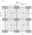
Figure 13A shows a plan view of a portion of a
画素セル1302は、n型カソード層1305の下に形成されたp-アノード層上に、n型カソード層1305で形成されたSPADを含んでいる。画素セル1302は、DTI壁を境界とする、先に記載したようなアノード層304を有する。アノード層304は、前述したように、アノード電極1308から相互接続パッド212dに連結されている。画素セル1302の中心を通る垂直断面は、図10Dの断面図1050と同様である。カソード電極1310は、トランジスタ領域1306a内の対応するpMOS再充電トランジスタ及びnMOSゲートトランジスタへの接続1312a及び1312bを有する。
The
図13Bは、画素ウエハ1300のトランジスタ区分1306aの拡大平面図1320を示す。トランジスタ区分1306a内には、nMOSゲートトランジスタ218と直列に配置されており、図2の画素セル210内に配置され得る回路を形成しているように接続された、pMOS HVクエンチングトランジスタ216が存在する。pMOS HVクエンチングトランジスタ216は、DNW1322内に形成されたNW1324内に形成されている。nMOSゲートトランジスタ218は、NW1326内に形成される。
FIG. 13B shows an
更に、pMOS再充電トランジスタ及びnMOSゲートトランジスタは、トランジスタ領域1306a内に順次配置されており、画素セルで示される最上列内の他の画素セルと関連付けられる。同様に、更なるpMOS再充電トランジスタ及びnMOSゲートトランジスタは、トランジスタ領域1306a内に順次配置され得、図13Aに示される画素セルの第2の列内の他の画素セルと関連付けられる。
Further, a pMOS recharge transistor and an nMOS gate transistor are sequentially arranged in
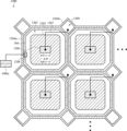
図14Aは、画素アレイ1400の平面図を示す。画素アレイ1400は、図13A~13Bに関連して説明された実施形態の変形形態として構成される。各画素セルのSPADがトランジスタ領域内に位置する3つの制御トランジスタと接続して、画素セル802内に図8Aに示す回路を形成しているように適応されている。画素アレイ1400は、画素セル1402などの画素セルの長方形アレイを含んでいる。水平方向に配向されたトランジスタ領域1406a~1406bは、画素セルの長方形アレイの列と交互になっている。水平DTI壁1404a及び1404bなどの水平DTI壁は、トランジスタ領域1406a~1406bと、画素セルの長方形アレイの列との間の分離を形成している。垂直DTI壁1404c~1404dなどの垂直DTI壁は、画素セルの長方形アレイの各列内に画素セル間の分離を形成し、画素セルの長方形アレイの列の画素セル間のトランジスタ領域1406cなどのトランジスタ領域を形成している。
Figure 14A shows a plan view of a
画素セル1402は、画素セル1402を取り囲むDTI壁に隣接する、上述したようなアノード層を含むことができる。画素セル1402は、図14Bに詳細に示されるように、カソード電極1410を介して、トランジスタ領域1406a及び1406c内に配置された3つの制御トランジスタに接続されたn型カソード層1408を有するSPADを含んでいる。図示の実施形態では、画素セル1402に関連付けられたnMOSゲートトランジスタ820及びpMOS再充電トランジスタ818は、水平方向に延在しているトランジスタ領域1406a内に配置されており、画素セル1402に関連する内部pMOSトランジスタ814は、トランジスタ領域1406c内に配置されている。
図14Bは、画素アレイ1400の画素セル1402と、トランジスタ領域1406a及び1406cとの拡大平面図1420を示す。平面図1420に示される構成及び接続は、図8Aの画素セル802内の回路を実装する。画素セル1402のSPADのn型カソード層1408は、接続部1412aによってカソード電極1410から、nMOSゲートトランジスタ820のドレインに接続する。nMOSゲートトランジスタ820は、DNW1422に形成されたPW1424内に形成されている。画素セル1402のSPADのn型カソード層1408は、接続部1412bによってカソード電極1410から、pMOS再充電トランジスタ818のドレインに接続する。pMOS再充電トランジスタ818は、NW1426内に形成されている。内部pMOSトランジスタ814は、NW1428内のトランジスタ領域1406c内に形成され、接続線1412bによってカソード電極1410に接続されている。他の態様では、図14Bに示された残りの構成要素の接続は、図8Aに示す回路図に記載されているとおりである。
14B shows an
第5のファミリー:別個のウエハ上の制御トランジスタ 5th family: control transistors on separate wafers
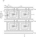
別の実施形態のセットは、3つの異なるウエハ;画素セルのアレイを含む画素アレイウエハ、制御トランジスタなどのバイアス及び制御回路素子を含み得る制御回路ウエハ、及び処理構成要素を含み得る論理回路ウエハ、を接合することによって形成される光感知及びイメージングデバイスを対象とする。このような処理構成要素としては、フィルタ、ヒストグラムカウンタ、画像若しくは他のデジタルプロセッサ、マイクロプロセッサ、又は更に他の構成要素を挙げることができるが、これらに限定されない。制御回路ウエハは、高電圧ソースから動作し得る画素セル内のSPAD用のゲートトランジスタ又は制御トランジスタなどの回路素子を含むことができる。特定の制御トランジスタを使用して、出力が論理回路ウエハに接続されたインバータ回路を実装することができる。 Another set of embodiments is directed to a light sensing and imaging device formed by bonding three different wafers; a pixel array wafer containing an array of pixel cells, a control circuit wafer that may contain bias and control circuit elements such as control transistors, and a logic wafer that may contain processing components. Such processing components may include, but are not limited to, filters, histogram counters, image or other digital processors, microprocessors, or even other components. The control circuit wafer may contain circuit elements such as gate or control transistors for SPADs in pixel cells that may operate from a high voltage source. Certain control transistors may be used to implement inverter circuits whose outputs are connected to the logic wafer.
図15Aは、SPAD1508に対応する論理回路ウエハ1502と画素アレイウエハ1506との間に配置された制御回路ウエハ1504の特定の構成要素の構成1500の回路図である。ウエハは、n型又はp型のいずれかであり得る、個別の半導体基板内に形成され得る。論理回路ウエハ1502は、電圧信号VBPによって制御されるゲートを有する、pMOSクエンチングトランジスタ1509を含むことができる。pMOSクエンチングトランジスタ1509は、電源ライン1512a上の低レベル電源電圧VDDLに接続されたソースを有し得る。pMOSクエンチングトランジスタのドレインは、相互接続パッド1510aを介して制御回路ウエハに接続する。論理回路ウエハ1502は、更なる回路素子を含むことができる。
15A is a circuit diagram of an
画素アレイウエハ1506は、画素セルのアレイを含んでもよく、画素セルのうちの少なくとも一部は、光検出用のSPAD1508などのSPADを含み得る。画素セル1506は、貫通シリコンビア(TSV)1519aにおいて、相互接続パッド1510eを介して、制御回路ウエハ1504に供給される、バイアス電圧源VSPADに接続され得る。SPAD1508のアノードは、別のTSV1519bによって制御回路ウエハ1504に接続することができる。SPAD1508のカソードは、TSV1519aにおいて受信されるバイアス電圧源VSPADに接続することができる。
The
制御回路ウエハ1504は、画素アレイウエハ1506のそれぞれのSPADの集光又は検出動作を制御する制御トランジスタを含むことができる。図示の実施形態では、制御回路ウエハ1504は、図8Aに示す制御回路を実装する3つの制御トランジスタを含んでいる。相互接続パッド1510cに連結されたゲート1513を有し外部制御回路から入力を受信するpMOS再充電トランジスタ1514と、相互接続パッド1510bに接続されたゲート1517を有するpMOS高電圧クエンチングトランジスタ1518と、相互接続パッド1510dに接続されたゲート1515を有するnMOSゲートトランジスタ1516と、が存在する。これらのトランジスタ及びそれらの相互接続の説明は、図8Aに関する説明と類似しており、ここでは繰り返さない。
The
図15Bは、SPAD1508を含む画素セルの構成と、pMOS再充電トランジスタ1514、pMOS高電圧クエンチングトランジスタ1518、及びnMOSゲートトランジスタ1516の構成又はレイアウトと、を示す拡大平面図1520である。nMOSゲートトランジスタ1516は、DNW1526内に形成されたPW1528内に形成されている。pMOS高電圧クエンチングトランジスタ1518は、NW1530内に形成されている。pMOS再充電トランジスタ1514は、NW1532内に形成されている。
FIG. 15B is an expanded
図15Cは、図15Bの切断線A-A’に沿った、画素アレイウエハ1506と接合又は結合された制御回路ウエハ1504の断面図1540である。SPAD1508は、n型カソード層1508aとp-アノード層1508bとの接合部として形成され得る。SPAD1508の画素セルは、前述されたような絶縁層302によって画素アレイウエハ1506の他の画素セルから絶縁され得る。絶縁層302の内部は、前述されたようなアノード層304であり得る。画素セル内の半導体基板は、p型であってもよく、ドーピング輪郭線1507a~1507cによって示されるような、ドーピング勾配を有し得る。
Figure 15C is a
画素アレイウエハ1506は、中間層1541と接合又は結合されて、制御回路ウエハ1544に接合又は結合される第1の組み合わせ層1542を形成していることができる。TSV1519は、SPAD1508と制御回路ウエハ1544の制御トランジスタとの間に電気的接続を提供し得る。論理回路ウエハ1502は、制御回路ウエハ1544の上面1546に接合又は結合され得る。
The
制御回路ウエハ1544内で、pMOS高電圧クエンチングトランジスタ1518は絶縁構造体1548a上に配置され得、nMOSゲートトランジスタ1516は絶縁構造体1548b上に配置され得る。ノード1521は、制御回路ウエハ1504の半導体基板に埋設された導体として実装することができる。
In the
図16は、図15A~15Cに関連して説明した実施形態の変形例を示す。図16の実施形態は、3つの接合又は結合されたウエハ:制御トランジスタを有さないSPAD画素セルのアレイを含む画素ウエハと、高電圧であり得る制御トランジスタを含む中間ウエハと、論理回路ウエハと、を使用する。図16の実施形態は、インバータ用のトランジスタが中間ウエハ上に位置している点で、図15A~15Cとは異なる。後述するように、SPAD画素は、図15Bに関連して開示されるように実装され得、ゲートトランジスタ、再充電トランジスタ及びインバータトランジスタの構成は、図9Dに関連して開示されるように実装され得る。 Figure 16 shows a variation of the embodiment described in connection with Figures 15A-15C. The embodiment of Figure 16 uses three bonded or joined wafers: a pixel wafer containing an array of SPAD pixel cells without control transistors, an intermediate wafer containing control transistors that may be high voltage, and a logic wafer. The embodiment of Figure 16 differs from Figures 15A-15C in that the transistors for the inverter are located on the intermediate wafer. As described below, the SPAD pixel may be implemented as disclosed in connection with Figure 15B, and the configuration of the gate transistors, recharge transistors, and inverter transistors may be implemented as disclosed in connection with Figure 9D.
図16は、論理回路ウエハ1601、中間ウエハ1605、及び画素ウエハ1611の構成要素の構成1600を示す。中間ウエハ1605は、画素ウエハ1611上に位置する1つ以上のSPADの制御トランジスタを含んでいる。この実施形態では、画素ウエハ1611は、SPAD1612などのSPADをそれぞれ含む画素セルのアレイを含んでいる。この実施形態では、中間ウエハ1605は、少なくとも再充電トランジスタ1606、ゲートトランジスタ1610、及びインバータ1608を含んでいる。インバータ1608は、図9Cに示すように、積層されたpMOSトランジスタ及びnMOSトランジスタとして形成されてもよく、又はトランジスタの別の構成で実装されてもよい。画素ウエハ1611は、貫通シリコンビア1613a及び1613bによるか、論理回路ウエハ1601を中間ウエハ1605に接続する1603などの金属ー金属接続によるか、又は別の構造によって、中間ウエハ1605と接合され得る。論理回路ウエハ1601は、少なくとも1ショット1602を含み、インバータ1608から受信した信号に基づいて標準パルスを生成する。標準パルスは、ヒストグラムカウンタ1604によって受信される。ヒストグラムカウンタ1604に加えて、論理回路ウエハ1601は、画像データを生成するように動作し得るマイクロプロセッサ、マイクロコントローラ、シグナルプロセッサ、メモリユニットなどの他の関連する論理回路を含むことができる。
16 shows a
構成1600の実施形態では、画素アレイ1611の画素セルのうちの少なくとも一部は、関連する制御トランジスタを含んでいない。この実施形態では、このような画素セルは、図15Bに示され、前述された構造を有し得る。
In an embodiment of
構成1600の中間ウエハ1605では、再充電トランジスタ1606、ゲートトランジスタ1610、及びインバータ1608の2つのトランジスタは、図9Dに示され、前述された半導体構成で配置及び実装され得る。中間ウエハ1605では、4つのトランジスタのそのような実装は、SPAD1612に関連する4つのトランジスタの各セットを分離するために、同じ構造又は代替の構造を使用することができる。
In
前述の記載では、説明のために、記載された実施形態の完全な理解をもたらすために特定の専門用語を用いた。しかし、記述される実施形態を実施するために、具体的な詳細は必要とされないことは、当業者には明らかであろう。従って、本明細書に述べられる特定の実施形態の前述の説明は、図示及び説明の目的で提示されている。これらの説明は、網羅的であること、又は開示されるまさにその形態に実施形態を限定することをターゲットとしたものではない。上記の教示を考慮すれば、多くの変更及び変形が可能であることが、当業者には明らかであろう。 In the foregoing description, for purposes of explanation, specific terminology was used to provide a thorough understanding of the described embodiments. However, it will be apparent to one skilled in the art that specific details are not required to practice the described embodiments. Thus, the foregoing description of the specific embodiments described herein has been presented for purposes of illustration and description. These descriptions are not intended to be exhaustive or to limit the embodiments to the precise forms disclosed. It will be apparent to one skilled in the art that many modifications and variations are possible in light of the above teachings.
Claims (14)
前記画素は、前記画素の側面を形成し、前記画素アレイの上面と前記上面の反対側の前記画素アレイの集光面との間で、前記画素アレイの半導体基板を少なくとも部分的に通って延在している絶縁壁と、
前記上面に隣接するカソード層、及び前記半導体基板内に埋め込まれ、前記上面の反対側の前記カソード層の側面上に隣接して堆積されたアノード層を、含む単一光子アバランシェダイオード(SPAD)と、
前記上面に隣接し、前記SPADと電気的に接続された制御トランジスタであって、前記アノード層の外側に、かつ少なくとも部分的に前記カソード層内に形成され、または少なくとも部分的に前記カソード層と前記上面との間に形成された制御トランジスタと、を備え、
前記アノード層と前記カソード層との間の界面にアバランシェ接合領域が存在し、前記アバランシェ接合領域は、少なくとも部分的に、前記制御トランジスタの下に延長している、画素アレイの画素。 A pixel of a pixel array, comprising:
the pixels each include an insulating wall forming a side of the pixel and extending at least partially through a semiconductor substrate of the pixel array between a top surface of the pixel array and a light collecting surface of the pixel array opposite the top surface;
a single photon avalanche diode (SPAD) including a cathode layer adjacent the top surface and an anode layer embedded within the semiconductor substrate and deposited adjacent on a side of the cathode layer opposite the top surface;
a control transistor adjacent to the top surface and electrically connected to the SPAD , the control transistor being formed outside the anode layer and at least partially within the cathode layer or at least partially between the cathode layer and the top surface ;
A pixel of a pixel array , wherein an avalanche junction region exists at an interface between the anode layer and the cathode layer, the avalanche junction region extending at least partially beneath the control transistor.
前記画素は、第2の制御トランジスタを更に備え、
前記第1の制御トランジスタがゲートトランジスタであり、
前記第2の制御トランジスタは、前記SPADに電気的に接続されているクエンチングトランジスタである、請求項1に記載の画素。 the control transistor is a first control transistor,
The pixel further comprises a second control transistor;
the first control transistor is a gating transistor;
The pixel of claim 1 , wherein the second control transistor is a quenching transistor electrically connected to the SPAD.
前記深いp-ウェル領域は、内部n-ウェル領域を含み、
前記クエンチングトランジスタが、前記内部n-ウェル領域内に形成されたpMOSトランジスタであり、
前記ゲートトランジスタは、前記p-ウェル領域内に形成されたnMOSトランジスタである、請求項2に記載の画素。 a p-well region; and a deep p-well region separated from the p-well region;
the deep p-well region includes an interior n-well region;
the quenching transistor is a pMOS transistor formed in the internal n-well region;
The pixel of claim 2 , wherein the gating transistor is an nMOS transistor formed in the p-well region.
前記クエンチングトランジスタは、前記第1のp-ウェル領域内に形成された第1のnMOSトランジスタであり、
前記ゲートトランジスタは、前記第2のp-ウェル領域内に形成された第2のnMOSトランジスタである、請求項2に記載の画素。 a first p-well region and a second p-well region;
the quenching transistor is a first nMOS transistor formed in the first p-well region;
The pixel of claim 2 , wherein the gating transistor is a second nMOS transistor formed in the second p-well region.
前記半導体基板は、n型であり、
前記クエンチングトランジスタが、前記第1のp-ウェル領域内に形成された第1のnMOSトランジスタであり、
前記ゲートトランジスタは、前記第2のp-ウェル領域に形成された第2のnMOSトランジスタである、請求項2に記載の画素。 a first deep n-well region including a first p-well region and a second deep n-well region including a second p-well region;
the semiconductor substrate is n-type;
the quenching transistor is a first nMOS transistor formed in the first p-well region;
The pixel of claim 2 , wherein the gating transistor is a second nMOS transistor formed in the second p-well region.
前記画素は、第2の制御トランジスタを更に含み、
前記画素は、第3の制御トランジスタを更に含み、
前記第1の制御トランジスタは、前記SPADの第1の電圧ソースとカソードとの間に電気的に接続されたクエンチングトランジスタであり、
前記第2の制御トランジスタは再充電トランジスタであり、
前記第3の制御トランジスタはゲートトランジスタであり、
前記再充電トランジスタは、共通ノードにおいて、第2の電圧ソースと第3の電圧ソースとの間の前記ゲートトランジスタと直列に接続されており、
前記SPADの前記カソードが、前記共通ノードに接続されている、請求項1に記載の画素。 the control transistor is a first control transistor,
the pixel further includes a second control transistor;
the pixel further includes a third control transistor;
the first control transistor is a quenching transistor electrically connected between a first voltage source and a cathode of the SPAD;
the second control transistor is a recharge transistor;
the third control transistor is a gating transistor;
the recharge transistor is connected in series with the gating transistor between a second voltage source and a third voltage source at a common node;
The pixel of claim 1 , wherein the cathode of the SPAD is connected to the common node.
前記ゲートトランジスタは、前記p-ウェル領域に形成されたnMOSトランジスタであり、
前記再充電トランジスタは、前記第1のn-ウェル領域内に形成された第1のpMOSトランジスタであり、
前記クエンチングトランジスタは、前記第2のn-ウェル領域に形成された第2のpMOSトランジスタである、請求項6に記載の画素。 a deep p-well region including a first n-well region, a second n-well region separated from the first n-well region, and a p-well region;
the gate transistor is an nMOS transistor formed in the p-well region,
the recharge transistor is a first pMOS transistor formed in the first n-well region;
The pixel of claim 6 , wherein the quenching transistor is a second pMOS transistor formed in the second n-well region.
前記ゲートトランジスタは、前記第1のn-ウェル領域に形成された第1のpMOSトランジスタであり、
前記再充電トランジスタは、前記第2のn-ウェル領域内に形成された第2のpMOSトランジスタであり、
前記クエンチングトランジスタは、前記第3のn-ウェル領域に形成された第3のpMOSトランジスタである、請求項6に記載の画素。 a first deep p-well region including the first n-well region, a second deep p-well region including the second n-well region, and a third deep p-well region including the third n-well region;
the gating transistor is a first pMOS transistor formed in the first n-well region;
the recharge transistor is a second pMOS transistor formed in the second n-well region;
The pixel of claim 6 , wherein the quenching transistor is a third pMOS transistor formed in the third n-well region.
前記浅いトレンチ絶縁材料は、前記画素の第1の領域と、前記画素の第2の領域と、前記画素の第3の領域とを分離しており、
前記クエンチングトランジスタが、前記第1の領域内に形成されており、
前記SPADの前記アノード層及び前記カソード層は、少なくとも部分的に前記第2の領域内に形成されており、
前記ゲートトランジスタ及び前記再充電トランジスタは、前記第3の領域内に形成されている、請求項6に記載の画素。 a shallow trench isolation material extending at least partially into the semiconductor substrate from the top surface;
the shallow trench isolation material separates the pixel first region, the pixel second region, and the pixel third region;
the quenching transistor is formed in the first region;
the anode layer and the cathode layer of the SPAD are formed at least partially within the second region;
The pixel of claim 6 , wherein the gating transistor and the recharge transistor are formed in the third region.
半導体基板と、
画素セルの長方形アレイと、
複数のトランジスタ領域と、
前記画素ウエハの前記上面から前記裏面に近接して前記半導体基板内に延在している深いトレンチ絶縁材料と、を備え、
画素セルの前記長方形アレイの各画素セルが、単一光子アバランシェダイオード(SPAD)を含み、
各トランジスタ領域は、対応する画素セルと関連付けられており、
各トランジスタ領域は、前記トランジスタ領域が関連付けられている前記対応する画素セルの前記SPADと電気的に接続された制御トランジスタを含み、
前記深いトレンチ絶縁材料は、画素セルの前記長方形アレイの各画素セルの周囲の側面を形成し、
各トランジスタ領域は、前記深いトレンチ絶縁材料によって、画素セルの前記長方形アレイの各画素セルから分離されており、
各トランジスタ領域は、画素セルの前記長方形アレイの格子点位置に位置し、かつ画素セルの前記長方形アレイに対して斜めに配向された長方形領域であり、
画素セルの前記長方形アレイの各画素セルの前記SPADは、前記上面に近接するn型カソードと、前記上面の反対側の前記n型カソードの下に形成されたp型アノードとを備えて形成されており、
前記半導体基板は、ドーピング勾配を有するp型であり、
各トランジスタ領域の前記制御トランジスタは、前記トランジスタ領域が関連付けられている前記対応する画素セルの前記SPADの集光動作を制御する、画素ウエハ。 A pixel wafer having a top surface and a back surface opposite the top surface,
A semiconductor substrate;
a rectangular array of pixel cells;
a plurality of transistor regions;
a deep trench isolation material extending into the semiconductor substrate from the top surface of the pixel wafer proximate the back surface;
each pixel cell of the rectangular array of pixel cells includes a single photon avalanche diode (SPAD);
Each transistor region is associated with a corresponding pixel cell;
each transistor region includes a control transistor electrically connected to the SPAD of the corresponding pixel cell with which the transistor region is associated;
the deep trench isolation material forms a peripheral sidewall of each pixel cell of the rectangular array of pixel cells;
each transistor region is separated from each pixel cell of the rectangular array of pixel cells by the deep trench isolation material;
each transistor region is a rectangular region located at a lattice point location of the rectangular array of pixel cells and oriented obliquely with respect to the rectangular array of pixel cells;
the SPAD of each pixel cell of the rectangular array of pixel cells is formed with an n-type cathode adjacent to the top surface and a p-type anode formed below the n-type cathode on an opposite side of the top surface;
the semiconductor substrate is p-type with a doping gradient;
A pixel wafer, wherein the control transistor of each transistor region controls the light collecting operation of the SPAD of the corresponding pixel cell with which the transistor region is associated.
前記第1のトランジスタ領域が、前記対応する画素セルの前記SPADの前記n型カソードと第2の電圧源との間に接続された、pMOSクエンチングトランジスタを含む、請求項10に記載の画素ウエハ。 the control transistor of a first transistor region of the plurality of transistor regions is an nMOS gate transistor connected between the n-type cathode of the SPAD of the corresponding pixel cell and a first voltage source;
The pixel wafer of claim 10 , wherein the first transistor region includes a pMOS quenching transistor connected between the n-type cathode of the SPAD of the corresponding pixel cell and a second voltage source.
半導体基板と、画素セルの長方形アレイとを備え、
少なくとも1つの画素セルは、
前記半導体基板の隣接する異なる層内に形成されたカソード及び埋め込まれたアノードを含む単一光子アバランシェダイオード(SPAD)と、
前記上面に近接して、前記アノードの外側に、かつ少なくとも部分的に前記カソード内に、または少なくとも部分的に前記カソードと前記上面との間に形成された制御トランジスタのグループとを含み、
前記制御トランジスタのグループが、前記SPADの再充電トランジスタと、前記SPADのゲートトランジスタと、前記SPADの前記カソードに接続された入力を有するインバータ回路を形成している第1のトランジスタ及び第2のトランジスタとを含み、
前記アノードと前記カソードとの間の界面にアバランシェ接合領域が存在し、前記アバランシェ接合領域は、少なくとも部分的に、前記制御トランジスタのグループのトランジスタの下に延長している、画素ウエハ。 A pixel wafer having a top surface and a back surface opposite the top surface,
a semiconductor substrate and a rectangular array of pixel cells;
At least one pixel cell comprises:
a single photon avalanche diode (SPAD) including a cathode and a buried anode formed in different adjacent layers of the semiconductor substrate;
a group of control transistors formed adjacent said top surface , outside said anode, and at least partially within said cathode, or at least partially between said cathode and said top surface ;
the group of control transistors includes a recharge transistor of the SPAD, a gating transistor of the SPAD, and first and second transistors forming an inverter circuit having an input connected to the cathode of the SPAD;
a pixel wafer , wherein an avalanche junction region exists at an interface between said anode and said cathode, said avalanche junction region extending at least partially under a transistor of said group of control transistors.
Priority Applications (2)
| Application Number | Priority Date | Filing Date | Title |
|---|---|---|---|
| JP2024061394A JP7738123B2 (en) | 2020-09-25 | 2024-04-05 | Transistor integration with stacked single-photon avalanche diode (SPAD) pixel arrays |
| JP2025144471A JP2025178258A (en) | 2020-09-25 | 2025-09-01 | Transistor integration with stacked single-photon avalanche diode (SPAD) pixel arrays |
Applications Claiming Priority (4)
| Application Number | Priority Date | Filing Date | Title |
|---|---|---|---|
| US202063083262P | 2020-09-25 | 2020-09-25 | |
| US63/083,262 | 2020-09-25 | ||
| US17/473,855 US12356740B2 (en) | 2020-09-25 | 2021-09-13 | Transistor integration with stacked single-photon avalanche diode (SPAD) pixel arrays |
| US17/473,855 | 2021-09-13 |
Related Child Applications (1)
| Application Number | Title | Priority Date | Filing Date |
|---|---|---|---|
| JP2024061394A Division JP7738123B2 (en) | 2020-09-25 | 2024-04-05 | Transistor integration with stacked single-photon avalanche diode (SPAD) pixel arrays |
Publications (2)
| Publication Number | Publication Date |
|---|---|
| JP2022054459A JP2022054459A (en) | 2022-04-06 |
| JP7555893B2 true JP7555893B2 (en) | 2024-09-25 |
Family
ID=80791627
Family Applications (3)
| Application Number | Title | Priority Date | Filing Date |
|---|---|---|---|
| JP2021156525A Active JP7555893B2 (en) | 2020-09-25 | 2021-09-27 | Transistor integration with stacked single-photon avalanche diode (SPAD) pixel arrays |
| JP2024061394A Active JP7738123B2 (en) | 2020-09-25 | 2024-04-05 | Transistor integration with stacked single-photon avalanche diode (SPAD) pixel arrays |
| JP2025144471A Pending JP2025178258A (en) | 2020-09-25 | 2025-09-01 | Transistor integration with stacked single-photon avalanche diode (SPAD) pixel arrays |
Family Applications After (2)
| Application Number | Title | Priority Date | Filing Date |
|---|---|---|---|
| JP2024061394A Active JP7738123B2 (en) | 2020-09-25 | 2024-04-05 | Transistor integration with stacked single-photon avalanche diode (SPAD) pixel arrays |
| JP2025144471A Pending JP2025178258A (en) | 2020-09-25 | 2025-09-01 | Transistor integration with stacked single-photon avalanche diode (SPAD) pixel arrays |
Country Status (4)
| Country | Link |
|---|---|
| US (2) | US12356740B2 (en) |
| JP (3) | JP7555893B2 (en) |
| KR (1) | KR102688418B1 (en) |
| CN (1) | CN114256276A (en) |
Families Citing this family (7)
| Publication number | Priority date | Publication date | Assignee | Title |
|---|---|---|---|---|
| JP7685533B2 (en) * | 2021-02-02 | 2025-05-29 | ソニーセミコンダクタソリューションズ株式会社 | Optical detection device and ranging system |
| CN114068512A (en) * | 2021-11-18 | 2022-02-18 | 武汉新芯集成电路制造有限公司 | Semiconductor device and semiconductor chip |
| US20230299109A1 (en) * | 2022-03-18 | 2023-09-21 | Taiwan Semiconductor Manufacturing Company, Ltd. | Stacked image sensors and methods of manufacturing thereof |
| US12408466B2 (en) * | 2022-07-11 | 2025-09-02 | Taiwan Semiconductor Manufacturing Company, Ltd. | High-speed readout image sensor |
| WO2024150531A1 (en) | 2023-01-13 | 2024-07-18 | ソニーセミコンダクタソリューションズ株式会社 | Light detection device |
| KR102735202B1 (en) * | 2023-02-13 | 2024-11-28 | 주식회사 솔리드뷰 | Analog Front End(AFE) device and control method for the same |
| JP2025009160A (en) * | 2023-07-07 | 2025-01-20 | ソニーセミコンダクタソリューションズ株式会社 | Photoelectric conversion device |
Citations (8)
| Publication number | Priority date | Publication date | Assignee | Title |
|---|---|---|---|---|
| US20100127314A1 (en) | 2007-04-24 | 2010-05-27 | Koninklijke Philips Electronics N.V. | Photodiodes and fabrication thereof |
| JP2014225647A (en) | 2013-04-01 | 2014-12-04 | オムニヴィジョン テクノロジーズ インコーポレイテッド | Enhanced photon detection device with biased deep trench isolation |
| JP2016511539A (en) | 2013-01-31 | 2016-04-14 | アップル インコーポレイテッド | Vertical stacked image sensor |
| JP2019169643A (en) | 2018-03-23 | 2019-10-03 | パナソニックIpマネジメント株式会社 | Solid state image sensor |
| JP2020039017A (en) | 2018-08-31 | 2020-03-12 | ソニーセミコンダクタソリューションズ株式会社 | Solid-state imaging device and method of driving the same, and electronic equipment |
| JP2020510308A (en) | 2017-03-01 | 2020-04-02 | ジーレイ スイッツァーランド エスアー | Electromagnetic absorption radiation detector based on wafer bonding |
| JP2020143959A (en) | 2019-03-05 | 2020-09-10 | ソニーセミコンダクタソリューションズ株式会社 | Control circuit and ranging system |
| JP2020155783A (en) | 2016-09-23 | 2020-09-24 | アップル インコーポレイテッドApple Inc. | Laminated back-illuminated SPAD array |
Family Cites Families (263)
| Publication number | Priority date | Publication date | Assignee | Title |
|---|---|---|---|---|
| JPH0668526B2 (en) | 1986-11-21 | 1994-08-31 | 日産自動車株式会社 | Frequency measuring device |
| US5056914A (en) | 1990-07-12 | 1991-10-15 | Ball Corporation | Charge integration range detector |
| US5179286A (en) | 1990-10-05 | 1993-01-12 | Mitsubishi Denki K.K. | Distance measuring apparatus receiving echo light pulses |
| JPH04363264A (en) | 1991-05-27 | 1992-12-16 | Toshiba Corp | Optical printer |
| US5610416A (en) | 1995-02-16 | 1997-03-11 | Hewlett-Packard Company | Avalanche photodiode with epitaxially regrown guard rings |
| US6714239B2 (en) | 1997-10-29 | 2004-03-30 | Eastman Kodak Company | Active pixel sensor with programmable color balance |
| US6522395B1 (en) | 1999-04-30 | 2003-02-18 | Canesta, Inc. | Noise reduction techniques suitable for three-dimensional information acquirable with CMOS-compatible image sensor ICS |
| US6323942B1 (en) | 1999-04-30 | 2001-11-27 | Canesta, Inc. | CMOS-compatible three-dimensional image sensor IC |
| JP2001285717A (en) | 2000-03-29 | 2001-10-12 | Toshiba Corp | Solid-state imaging device |
| TW516184B (en) | 2000-06-20 | 2003-01-01 | Pixelplus Co Ltd | CMOS active pixel for improving sensitivity |
| JP4515617B2 (en) | 2000-10-23 | 2010-08-04 | 富士フイルム株式会社 | Solid-state imaging device and driving method thereof |
| US7554067B2 (en) | 2001-05-07 | 2009-06-30 | Panavision Imaging Llc | Scanning imager employing multiple chips with staggered pixels |
| US6791596B2 (en) | 2001-06-28 | 2004-09-14 | Ricoh Company, Ltd. | Method and apparatus for image forming capable of effectively generating pixel clock pulses |
| US7084914B2 (en) | 2001-07-20 | 2006-08-01 | Micron Technology, Inc. | Variable pixel clock electronic shutter control |
| KR100455286B1 (en) | 2002-01-11 | 2004-11-06 | 삼성전자주식회사 | Method and apparatus for understanding the condition of animal using acquisition and analysis of physiological signal of the animal |
| US7906826B2 (en) | 2002-02-05 | 2011-03-15 | E-Phocus | Many million pixel image sensor |
| CN1145245C (en) | 2002-03-22 | 2004-04-07 | 中国科学院上海光学精密机械研究所 | Device for adjusting laser pulse time width |
| KR100462182B1 (en) | 2002-04-15 | 2004-12-16 | 삼성전자주식회사 | Apparatus and method for detecting heart beat using ppg |
| JP2004048345A (en) | 2002-07-11 | 2004-02-12 | Niles Co Ltd | Imaging system |
| GB0216075D0 (en) | 2002-07-11 | 2002-08-21 | Qinetiq Ltd | Photodetector circuits |
| US7525168B2 (en) | 2002-08-27 | 2009-04-28 | E-Phocus, Inc. | CMOS sensor with electrodes across photodetectors at approximately equal potential |
| US7786543B2 (en) | 2002-08-27 | 2010-08-31 | E-Phocus | CDS capable sensor with photon sensing layer on active pixel circuit |
| US7471315B2 (en) | 2003-03-14 | 2008-12-30 | Aptina Imaging Corporation | Apparatus and method for detecting and compensating for illuminant intensity changes within an image |
| JP4131191B2 (en) | 2003-04-11 | 2008-08-13 | 日本ビクター株式会社 | Avalanche photodiode |
| US7075049B2 (en) | 2003-06-11 | 2006-07-11 | Micron Technology, Inc. | Dual conversion gain imagers |
| WO2005020798A2 (en) | 2003-08-27 | 2005-03-10 | Datex-Ohmeda, Inc. | Multi-domain motion estimation and plethysmographic recognition using fuzzy neural-nets |
| US7115855B2 (en) | 2003-09-05 | 2006-10-03 | Micron Technology, Inc. | Image sensor having pinned floating diffusion diode |
| US7154075B2 (en) | 2003-11-13 | 2006-12-26 | Micron Technology, Inc. | Method and apparatus for pixel signal binning and interpolation in column circuits of a sensor circuit |
| US7332786B2 (en) | 2003-11-26 | 2008-02-19 | Micron Technology, Inc. | Anti-blooming storage pixel |
| US7091466B2 (en) | 2003-12-19 | 2006-08-15 | Micron Technology, Inc. | Apparatus and method for pixel binning in an image sensor |
| US7437013B2 (en) | 2003-12-23 | 2008-10-14 | General Instrument Corporation | Directional spatial video noise reduction |
| US7446812B2 (en) | 2004-01-13 | 2008-11-04 | Micron Technology, Inc. | Wide dynamic range operations for imaging |
| US7102117B2 (en) | 2004-06-08 | 2006-09-05 | Eastman Kodak Company | Active pixel sensor cell with integrating varactor and method for using such cell |
| US7825973B2 (en) | 2004-07-16 | 2010-11-02 | Micron Technology, Inc. | Exposure control for image sensors |
| US7880785B2 (en) | 2004-07-21 | 2011-02-01 | Aptina Imaging Corporation | Rod and cone response sensor |
| JP4455215B2 (en) | 2004-08-06 | 2010-04-21 | キヤノン株式会社 | Imaging device |
| US7259413B2 (en) | 2004-09-28 | 2007-08-21 | Micron Technology, Inc. | High dynamic range image sensor |
| US7555158B2 (en) | 2004-12-07 | 2009-06-30 | Electronics And Telecommunications Research Institute | Apparatus for recovering background in image sequence and method thereof |
| US7502054B2 (en) | 2004-12-20 | 2009-03-10 | Pixim, Inc. | Automatic detection of fluorescent flicker in video images |
| US7190039B2 (en) | 2005-02-18 | 2007-03-13 | Micron Technology, Inc. | Microelectronic imagers with shaped image sensors and methods for manufacturing microelectronic imagers |
| JP4855704B2 (en) | 2005-03-31 | 2012-01-18 | 株式会社東芝 | Solid-state imaging device |
| JP4377840B2 (en) | 2005-03-31 | 2009-12-02 | イーストマン コダック カンパニー | Digital camera |
| US7443421B2 (en) | 2005-04-05 | 2008-10-28 | Hewlett-Packard Development Company, L.P. | Camera sensor |
| JP4207926B2 (en) | 2005-05-13 | 2009-01-14 | ソニー株式会社 | Flicker correction method, flicker correction apparatus, and imaging apparatus |
| TWI429066B (en) | 2005-06-02 | 2014-03-01 | 新力股份有限公司 | Semiconductor image sensor module and manufacturing method thereof |
| US7415096B2 (en) | 2005-07-26 | 2008-08-19 | Jordan Valley Semiconductors Ltd. | Curved X-ray reflector |
| JP4227152B2 (en) | 2005-08-02 | 2009-02-18 | 三星電機株式会社 | Active pixel array of CMOS image sensor |
| KR100775058B1 (en) | 2005-09-29 | 2007-11-08 | 삼성전자주식회사 | An image processing system including a pixel, an image sensor using the same, and the image sensor |
| US8355117B2 (en) | 2005-12-21 | 2013-01-15 | Ecole Polytechnique Federale De Lausanne | Method and arrangement for measuring the distance to an object |
| US7626626B2 (en) | 2006-01-13 | 2009-12-01 | Micron Technology, Inc. | Method and apparatus providing pixel storage gate charge sensing for electronic stabilization in imagers |
| US7714292B2 (en) | 2006-02-01 | 2010-05-11 | Koninklijke Philips Electronics N.V. | Geiger mode avalanche photodiode |
| JP4796408B2 (en) | 2006-03-03 | 2011-10-19 | 株式会社リコー | Image forming apparatus |
| US7667400B1 (en) | 2006-06-09 | 2010-02-23 | Array Optronix, Inc. | Back-illuminated Si photomultipliers: structure and fabrication methods |
| US8026966B2 (en) | 2006-08-29 | 2011-09-27 | Micron Technology, Inc. | Method, apparatus and system providing a storage gate pixel with high dynamic range |
| US7773138B2 (en) | 2006-09-13 | 2010-08-10 | Tower Semiconductor Ltd. | Color pattern and pixel level binning for APS image sensor using 2×2 photodiode sharing scheme |
| US8194148B2 (en) | 2006-09-14 | 2012-06-05 | Nikon Corporation | Image processing device, electronic camera and image processing program |
| KR100828943B1 (en) | 2006-12-19 | 2008-05-13 | (주)실리콘화일 | A 3T-4S step & repeat unit cell and an image sensor having the unit cell, a data storage device, a semiconductor process mask, a semiconductor wafer |
| US7742090B2 (en) | 2006-12-22 | 2010-06-22 | Palo Alto Research Center Incorporated | Flexible segmented image sensor |
| US7589316B2 (en) | 2007-01-18 | 2009-09-15 | Ethicon Endo-Surgery, Inc. | Scanning beam imaging with adjustable detector sensitivity or gain |
| US7796171B2 (en) | 2007-02-16 | 2010-09-14 | Flir Advanced Imaging Systems, Inc. | Sensor-based gamma correction of a digital camera |
| KR100835892B1 (en) | 2007-03-26 | 2008-06-09 | (주)실리콘화일 | Chip Stacked Image Sensor |
| JP4935486B2 (en) | 2007-04-23 | 2012-05-23 | ソニー株式会社 | Solid-state imaging device, driving method for solid-state imaging device, signal processing method for solid-state imaging device, and imaging device |
| JP5163935B2 (en) | 2007-05-17 | 2013-03-13 | ソニー株式会社 | Image sensor |
| KR100872991B1 (en) | 2007-06-25 | 2008-12-08 | 주식회사 동부하이텍 | Image sensor and manufacturing method |
| JP2009021809A (en) | 2007-07-11 | 2009-01-29 | Canon Inc | Imaging device driving method, imaging device, and imaging system |
| JP2009075068A (en) | 2007-08-08 | 2009-04-09 | Nuflare Technology Inc | Pattern inspection apparatus and pattern inspection method |
| US7696483B2 (en) | 2007-08-10 | 2010-04-13 | General Electric Company | High DQE photon counting detector using statistical recovery of pile-up events |
| JP2009054870A (en) | 2007-08-28 | 2009-03-12 | Sanyo Electric Co Ltd | Imaging device |
| US7873236B2 (en) | 2007-08-28 | 2011-01-18 | General Electric Company | Systems, methods and apparatus for consistency-constrained filtered backprojection for out-of-focus artifacts in digital tomosythesis |
| KR100887887B1 (en) | 2007-11-06 | 2009-03-06 | 주식회사 동부하이텍 | Image sensor |
| JP5163068B2 (en) | 2007-11-16 | 2013-03-13 | 株式会社ニコン | Imaging device |
| JP4971956B2 (en) | 2007-11-27 | 2012-07-11 | キヤノン株式会社 | Flicker correction apparatus, flicker correction method, and imaging apparatus |
| US8259228B2 (en) | 2007-12-10 | 2012-09-04 | Ati Technologies Ulc | Method and apparatus for high quality video motion adaptive edge-directional deinterlacing |
| US7952635B2 (en) | 2007-12-19 | 2011-05-31 | Teledyne Licensing, Llc | Low noise readout apparatus and method with snapshot shutter and correlated double sampling |
| JP5026951B2 (en) | 2007-12-26 | 2012-09-19 | オリンパスイメージング株式会社 | Imaging device driving device, imaging device driving method, imaging device, and imaging device |
| US9017748B2 (en) | 2007-12-28 | 2015-04-28 | Kraft Foods Group Brands Llc | Potassium fortification in foodstuffs |
| EP2398055B1 (en) | 2008-01-10 | 2012-12-12 | Stmicroelectronics Sa | Pixel circuit for global electronic shutter |
| US8891790B2 (en) | 2008-01-14 | 2014-11-18 | Apple Inc. | Methods for using an accessory to communicate with an electronic device |
| US8227844B2 (en) | 2008-01-14 | 2012-07-24 | International Business Machines Corporation | Low lag transfer gate device |
| US8874377B1 (en) | 2008-02-29 | 2014-10-28 | The United States Of America As Represented By The Secretary Of The Army | Photon counting based particles detection method and apparatus |
| US8116540B2 (en) | 2008-04-04 | 2012-02-14 | Validity Sensors, Inc. | Apparatus and method for reducing noise in fingerprint sensing circuits |
| JP4494492B2 (en) | 2008-04-09 | 2010-06-30 | キヤノン株式会社 | Solid-state imaging device and driving method of solid-state imaging device |
| BRPI0912721B8 (en) | 2008-05-14 | 2021-06-22 | Espenusa Holding Llc | physical activity data collection unit with two or more infrared sensors, at least one temperature sensor and at least one accelerometer |
| JP5188275B2 (en) | 2008-06-06 | 2013-04-24 | キヤノン株式会社 | Solid-state imaging device, driving method thereof, and imaging system |
| US8637875B2 (en) | 2008-07-11 | 2014-01-28 | The Regents Of The University Of California | Single photon IR detectors and their integration with silicon detectors |
| JP5300356B2 (en) | 2008-07-18 | 2013-09-25 | キヤノン株式会社 | IMAGING DEVICE AND IMAGING DEVICE CONTROL METHOD |
| KR101467509B1 (en) | 2008-07-25 | 2014-12-01 | 삼성전자주식회사 | Image sensor and operating method for image sensor |
| US8388346B2 (en) | 2008-08-30 | 2013-03-05 | Nokia Corporation | Tactile feedback |
| US7838956B2 (en) | 2008-12-17 | 2010-11-23 | Eastman Kodak Company | Back illuminated sensor with low crosstalk |
| US8164669B2 (en) | 2008-12-19 | 2012-04-24 | Truesense Imaging, Inc. | Charge-coupled device image sensor with efficient binning of same-color pixels |
| US8686952B2 (en) | 2008-12-23 | 2014-04-01 | Apple Inc. | Multi touch with multi haptics |
| US20100159632A1 (en) | 2008-12-23 | 2010-06-24 | Omnivision Technologies, Inc. | Technique for fabrication of backside illuminated image sensor |
| US8760413B2 (en) | 2009-01-08 | 2014-06-24 | Synaptics Incorporated | Tactile surface |
| US8340407B2 (en) | 2009-01-14 | 2012-12-25 | Cisco Technology, Inc. | System and method for image demosaicing |
| EP2211430A3 (en) | 2009-01-23 | 2015-05-27 | Board of Trustees of Michigan State University | Laser autocorrelation system |
| US8378310B2 (en) | 2009-02-11 | 2013-02-19 | Prismatic Sensors Ab | Image quality in photon counting-mode detector systems |
| US20120159996A1 (en) | 2010-12-28 | 2012-06-28 | Gary Edwin Sutton | Curved sensor formed from silicon fibers |
| US8184188B2 (en) | 2009-03-12 | 2012-05-22 | Micron Technology, Inc. | Methods and apparatus for high dynamic operation of a pixel cell |
| US8140143B2 (en) | 2009-04-16 | 2012-03-20 | Massachusetts Institute Of Technology | Washable wearable biosensor |
| US8089036B2 (en) | 2009-04-30 | 2012-01-03 | Omnivision Technologies, Inc. | Image sensor with global shutter and in pixel storage transistor |
| JP2011004390A (en) | 2009-05-18 | 2011-01-06 | Canon Inc | Imaging device, imaging system, and method for driving imaging device |
| US8350940B2 (en) | 2009-06-08 | 2013-01-08 | Aptina Imaging Corporation | Image sensors and color filter arrays for charge summing and interlaced readout modes |
| JP5681176B2 (en) | 2009-06-22 | 2015-03-04 | トヨタ モーター ヨーロッパ ナームロゼ フェンノートシャップ/ソシエテ アノニム | Optical distance meter using pulsed light |
| KR101597785B1 (en) | 2009-07-14 | 2016-02-25 | 삼성전자주식회사 | Image sensor and image processing method |
| US8755854B2 (en) | 2009-07-31 | 2014-06-17 | Nellcor Puritan Bennett Ireland | Methods and apparatus for producing and using lightly filtered photoplethysmograph signals |
| JP5625284B2 (en) | 2009-08-10 | 2014-11-19 | ソニー株式会社 | Solid-state imaging device, driving method of solid-state imaging device, and electronic apparatus |
| TWI423246B (en) | 2009-08-21 | 2014-01-11 | Primax Electronics Ltd | Image processing method and apparatus thereof |
| US8619163B2 (en) | 2009-09-18 | 2013-12-31 | Canon Kabushiki Kaisha | Solid state imaging using a correction parameter for correcting a cross talk between adjacent pixels |
| US9066660B2 (en) | 2009-09-29 | 2015-06-30 | Nellcor Puritan Bennett Ireland | Systems and methods for high-pass filtering a photoplethysmograph signal |
| US8194165B2 (en) | 2009-09-30 | 2012-06-05 | Truesense Imaging, Inc. | Methods for capturing and reading out images from an image sensor |
| JP2011091775A (en) | 2009-10-26 | 2011-05-06 | Toshiba Corp | Solid-state image pickup device |
| US8546737B2 (en) | 2009-10-30 | 2013-10-01 | Invisage Technologies, Inc. | Systems and methods for color binning |
| FI20096232A0 (en) | 2009-11-23 | 2009-11-23 | Valtion Teknillinen | Physical activity-based control for a device |
| JP2011123149A (en) | 2009-12-09 | 2011-06-23 | Ricoh Co Ltd | Optical scanning apparatus and image forming apparatus |
| TWI515885B (en) | 2009-12-25 | 2016-01-01 | 新力股份有限公司 | Semiconductor component, method of manufacturing the same, and electronic device |
| US9870053B2 (en) | 2010-02-08 | 2018-01-16 | Immersion Corporation | Systems and methods for haptic feedback using laterally driven piezoelectric actuators |
| US9451887B2 (en) | 2010-03-31 | 2016-09-27 | Nellcor Puritan Bennett Ireland | Systems and methods for measuring electromechanical delay of the heart |
| JP5641287B2 (en) | 2010-03-31 | 2014-12-17 | ソニー株式会社 | Solid-state imaging device, driving method of solid-state imaging device, and electronic apparatus |
| JP2011216673A (en) | 2010-03-31 | 2011-10-27 | Sony Corp | Solid-state imaging device, method for manufacturing of solid-state imaging device, and electronic apparatus |
| JP5516960B2 (en) | 2010-04-02 | 2014-06-11 | ソニー株式会社 | Solid-state imaging device, driving method of solid-state imaging device, and electronic apparatus |
| WO2011127343A2 (en) | 2010-04-08 | 2011-10-13 | Bae Systems Information And Electronic Systems Integration Inc. | Avalanche photodiode operating voltage selection algorithm |
| JP5602225B2 (en) | 2010-05-07 | 2014-10-08 | 三菱電機株式会社 | Laser radar equipment |
| EP2387229B1 (en) | 2010-05-14 | 2016-04-06 | Casio Computer Co., Ltd. | Image capturing apparatus and camera shake correction method, and computer-readable medium |
| KR101473424B1 (en) | 2010-06-01 | 2014-12-24 | 볼리 미디어 커뮤니케이션스 (센젠) 캄파니 리미티드 | Multispectral photoreceptive device and sampling method thereof |
| KR101198249B1 (en) | 2010-07-07 | 2012-11-07 | 에스케이하이닉스 주식회사 | Column circuit and pixel binning circuit of image sensor |
| WO2012011095A1 (en) | 2010-07-19 | 2012-01-26 | Yeda Research And Development Co. Ltd. | Linear optical characterization of ultrashort optical pulses |
| JP5682174B2 (en) | 2010-08-09 | 2015-03-11 | ソニー株式会社 | Solid-state imaging device, manufacturing method thereof, and electronic apparatus |
| US8338856B2 (en) | 2010-08-10 | 2012-12-25 | Omnivision Technologies, Inc. | Backside illuminated image sensor with stressed film |
| JP2012048080A (en) | 2010-08-30 | 2012-03-08 | Ricoh Co Ltd | Light source device, optical scanner and image forming device |
| GB201014843D0 (en) | 2010-09-08 | 2010-10-20 | Univ Edinburgh | Single photon avalanche diode for CMOS circuits |
| US9857469B2 (en) | 2010-10-22 | 2018-01-02 | Heptagon Micro Optics Pte. Ltd. | System and method for multi TOF camera operation using phase hopping |
| JP5589760B2 (en) | 2010-10-27 | 2014-09-17 | ソニー株式会社 | Image processing apparatus, imaging apparatus, image processing method, and program. |
| DE102010060527B3 (en) | 2010-11-12 | 2012-04-19 | Picoquant Gmbh | Switching arrangement for detecting single photon, has capacitive component and switching device connected to current path, and electrical component formed as electrical diode device that is aligned opposite to alignment of photodiode |
| US10120446B2 (en) | 2010-11-19 | 2018-11-06 | Apple Inc. | Haptic input device |
| JP5721405B2 (en) | 2010-11-22 | 2015-05-20 | キヤノン株式会社 | Imaging system, control method thereof, and program |
| JP5724322B2 (en) | 2010-11-24 | 2015-05-27 | ソニー株式会社 | Method for manufacturing solid-state imaging device |
| GB2485994A (en) | 2010-11-30 | 2012-06-06 | St Microelectronics Res & Dev | Navigation device using a Single Photon Avalanche Diode (SPAD) detector |
| JP5673063B2 (en) | 2010-12-15 | 2015-02-18 | ソニー株式会社 | Solid-state imaging device, driving method, and electronic apparatus |
| DE102010061382B4 (en) | 2010-12-21 | 2019-02-14 | Sick Ag | Opto-electronic sensor and method for detection and distance determination of objects |
| GB2486668A (en) | 2010-12-22 | 2012-06-27 | St Microelectronics Res & Dev | Real-time processing method and system for an optical range finder |
| EP2469301A1 (en) | 2010-12-23 | 2012-06-27 | André Borowski | Methods and devices for generating a representation of a 3D scene at very high speed |
| EP2469295A1 (en) | 2010-12-23 | 2012-06-27 | André Borowski | 3D landscape real-time imager and corresponding imaging methods |
| US8723975B2 (en) | 2011-01-24 | 2014-05-13 | Aptina Imaging Corporation | High-dynamic-range imaging devices |
| US8803990B2 (en) | 2011-01-25 | 2014-08-12 | Aptina Imaging Corporation | Imaging system with multiple sensors for producing high-dynamic-range images |
| JP2012169530A (en) | 2011-02-16 | 2012-09-06 | Sony Corp | Solid state image sensor, manufacturing method therefor, and electronic apparatus |
| JP5708025B2 (en) | 2011-02-24 | 2015-04-30 | ソニー株式会社 | Solid-state imaging device, manufacturing method thereof, and electronic apparatus |
| RU2589468C2 (en) | 2011-04-05 | 2016-07-10 | Конинклейке Филипс Н.В. | Matrix of detectors with analogue-to-digital conversion of time with higher time accuracy |
| US9088727B2 (en) | 2011-04-06 | 2015-07-21 | Pelco, Inc. | Spatially-varying flicker detection |
| KR101294386B1 (en) | 2011-04-13 | 2013-08-08 | 엘지이노텍 주식회사 | Pixel, pixel arrary, image sensor including the pixel arrary |
| US8575531B2 (en) | 2011-04-26 | 2013-11-05 | Aptina Imaging Corporation | Image sensor array for back side illumination with global shutter using a junction gate photodiode |
| JP6059722B2 (en) | 2011-08-03 | 2017-01-11 | コーニンクレッカ フィリップス エヌ ヴェKoninklijke Philips N.V. | Position sensitive readout mode for digital silicon photomultiplier tube arrays |
| JP2013055500A (en) | 2011-09-02 | 2013-03-21 | Sony Corp | Solid state imaging device and camera system |
| US8797512B2 (en) | 2011-09-15 | 2014-08-05 | Advanced Scientific Concepts, Inc. | Automatic range corrected flash ladar camera |
| JP5935274B2 (en) | 2011-09-22 | 2016-06-15 | ソニー株式会社 | Solid-state imaging device, control method for solid-state imaging device, and control program for solid-state imaging device |
| GB2494479A (en) | 2011-10-19 | 2013-03-13 | St Microelectronics Res & Dev | A proximity sensor with a cover for directing radiation from a radiation source to a reference radiation detector |
| US8594170B2 (en) | 2011-10-24 | 2013-11-26 | Sigear Europe Sarl | Clock masking scheme in a mixed-signal system |
| WO2013066959A1 (en) | 2011-10-31 | 2013-05-10 | The Trustees Of Columbia University In The City Of New York | Systems and methods for imaging using single photon avalanche diodes |
| JP5764466B2 (en) | 2011-11-04 | 2015-08-19 | ルネサスエレクトロニクス株式会社 | Solid-state imaging device |
| US8982237B2 (en) | 2011-12-09 | 2015-03-17 | Htc Corporation | Portable electronic device with auto-exposure control adaptive to environment brightness and image capturing method using the same |
| JP6239820B2 (en) | 2011-12-19 | 2017-11-29 | キヤノン株式会社 | Imaging apparatus and control method thereof |
| JP5497874B2 (en) | 2011-12-22 | 2014-05-21 | 富士フイルム株式会社 | Radiation image detector, radiation image capturing apparatus, and radiation image capturing system |
| JP5903894B2 (en) | 2012-01-06 | 2016-04-13 | 株式会社リコー | Optical scanning apparatus and image forming apparatus |
| FR2985570A1 (en) | 2012-01-09 | 2013-07-12 | St Microelectronics Grenoble 2 | DEVICE FOR DETECTING THE PROXIMITY OF AN OBJECT, COMPRISING SPAD PHOTODIODS |
| EP2624569B1 (en) | 2012-02-06 | 2016-09-28 | Harvest Imaging bvba | Method for correcting image data from an image sensor having image pixels and non-image pixels, and image sensor implementing the same |
| WO2013118111A1 (en) | 2012-02-12 | 2013-08-15 | El-Mul Technologies Ltd. | Position sensitive stem detector |
| JP6151530B2 (en) | 2012-02-29 | 2017-06-21 | 株式会社半導体エネルギー研究所 | Image sensor, camera, and surveillance system |
| FR2989518A1 (en) | 2012-04-13 | 2013-10-18 | St Microelectronics Crolles 2 | Method for manufacturing integrated image sensor, involves forming pixels at end of columns, and deforming structure such that another end of each of columns is brought closer or separated to form surface in shape of polyhedral cap |
| US9270906B2 (en) | 2012-05-02 | 2016-02-23 | Semiconductor Components Industries, Llc | Exposure time selection using stacked-chip image sensors |
| US10334181B2 (en) | 2012-08-20 | 2019-06-25 | Microsoft Technology Licensing, Llc | Dynamically curved sensor for optical zoom lens |
| US8817154B2 (en) | 2012-08-30 | 2014-08-26 | Omnivision Technologies, Inc. | Image sensor with fixed potential output transistor |
| US9448110B2 (en) | 2012-09-27 | 2016-09-20 | Northrop Grumman Systems Corporation | Three-dimensional hyperspectral imaging systems and methods using a light detection and ranging (LIDAR) focal plane array |
| JP6012375B2 (en) | 2012-09-28 | 2016-10-25 | 株式会社メガチップス | Pixel interpolation processing device, imaging device, program, and integrated circuit |
| JP6017916B2 (en) | 2012-10-16 | 2016-11-02 | 株式会社豊田中央研究所 | Photodetector |
| JP6225411B2 (en) | 2012-10-16 | 2017-11-08 | 株式会社豊田中央研究所 | Optical distance measuring device |
| GB201219781D0 (en) | 2012-11-02 | 2012-12-19 | St Microelectronics Res & Dev | Improvements in time of flight pixel circuits |
| FR2998666B1 (en) | 2012-11-27 | 2022-01-07 | E2V Semiconductors | METHOD FOR PRODUCING IMAGES WITH DEPTH INFORMATION AND IMAGE SENSOR |
| US9700240B2 (en) | 2012-12-14 | 2017-07-11 | Microsoft Technology Licensing, Llc | Physical activity inference from environmental metrics |
| CN103064076B (en) | 2012-12-26 | 2014-06-25 | 南京理工大学 | System and method for correction of distance walking error of photon counting three-dimensional imaging laser radar |
| US9164144B2 (en) | 2012-12-27 | 2015-10-20 | General Electric Company | Characterization and calibration of large area solid state photomultiplier breakdown voltage and/or capacitance |
| GB2510890A (en) | 2013-02-18 | 2014-08-20 | St Microelectronics Res & Dev | Method and apparatus |
| US8934030B2 (en) | 2013-02-20 | 2015-01-13 | Hewlett-Packard Development Company, L.P. | Suppressing flicker in digital images |
| JP6087674B2 (en) | 2013-02-27 | 2017-03-01 | キヤノン株式会社 | Imaging device |
| US9293500B2 (en) | 2013-03-01 | 2016-03-22 | Apple Inc. | Exposure control for image sensors |
| US9276031B2 (en) | 2013-03-04 | 2016-03-01 | Apple Inc. | Photodiode with different electric potential regions for image sensors |
| US9041837B2 (en) | 2013-03-05 | 2015-05-26 | Apple Inc. | Image sensor with reduced blooming |
| KR20140109668A (en) | 2013-03-06 | 2014-09-16 | 삼성전자주식회사 | Method and system for detecting flicker |
| US9741754B2 (en) | 2013-03-06 | 2017-08-22 | Apple Inc. | Charge transfer circuit with storage nodes in image sensors |
| KR102009189B1 (en) | 2013-03-12 | 2019-08-09 | 삼성전자주식회사 | Image Sensor and Method of simultaneously Reading out Two - Row Pixels thereof |
| US9549099B2 (en) | 2013-03-12 | 2017-01-17 | Apple Inc. | Hybrid image sensor |
| US9319611B2 (en) | 2013-03-14 | 2016-04-19 | Apple Inc. | Image sensor with flexible pixel summing |
| US9066017B2 (en) | 2013-03-25 | 2015-06-23 | Google Inc. | Viewfinder display based on metering images |
| JP6104049B2 (en) | 2013-05-21 | 2017-03-29 | オリンパス株式会社 | Image processing apparatus, image processing method, and image processing program |
| US9154750B2 (en) | 2013-05-28 | 2015-10-06 | Omnivision Technologies, Inc. | Correction of image sensor fixed-pattern noise (FPN) due to color filter pattern |
| JP2015012127A (en) | 2013-06-28 | 2015-01-19 | ソニー株式会社 | Solid-state imaging device and electronic device |
| GB2520232A (en) | 2013-08-06 | 2015-05-20 | Univ Edinburgh | Multiple Event Time to Digital Converter |
| JP6090060B2 (en) | 2013-08-23 | 2017-03-08 | 株式会社豊田中央研究所 | Single photon avalanche diode |
| US9344649B2 (en) | 2013-08-23 | 2016-05-17 | Semiconductor Components Industries, Llc | Floating point image sensors with different integration times |
| CN103472458B (en) | 2013-09-16 | 2015-04-15 | 中国科学院上海光学精密机械研究所 | Three-dimensional video laser radar system based on acousto-optic scanning |
| US9596420B2 (en) | 2013-12-05 | 2017-03-14 | Apple Inc. | Image sensor having pixels with different integration periods |
| US9473706B2 (en) | 2013-12-09 | 2016-10-18 | Apple Inc. | Image sensor flicker detection |
| US9312401B2 (en) | 2014-01-15 | 2016-04-12 | Omnivision Technologies, Inc. | Single photon avalanche diode imaging sensor for complementary metal oxide semiconductor stacked chip applications |
| US9331116B2 (en) * | 2014-01-15 | 2016-05-03 | Omnivision Technologies, Inc. | Back side illuminated single photon avalanche diode imaging sensor with high short wavelength detection efficiency |
| KR102135586B1 (en) | 2014-01-24 | 2020-07-20 | 엘지전자 주식회사 | Mobile terminal and method for controlling the same |
| JP6693880B2 (en) | 2014-01-29 | 2020-05-13 | エルジー イノテック カンパニー リミテッド | Depth information extraction device and method |
| CN103779437A (en) | 2014-02-17 | 2014-05-07 | 苏州超锐微电子有限公司 | Single-photon-level resolution ratio sensor unit structure based on standard CMOS technology |
| US10276620B2 (en) | 2014-02-27 | 2019-04-30 | Taiwan Semiconductor Manufacturing Co., Ltd. | Image sensor device and method for forming the same |
| US9277144B2 (en) | 2014-03-12 | 2016-03-01 | Apple Inc. | System and method for estimating an ambient light condition using an image sensor and field-of-view compensation |
| US9232150B2 (en) | 2014-03-12 | 2016-01-05 | Apple Inc. | System and method for estimating an ambient light condition using an image sensor |
| US9478030B1 (en) | 2014-03-19 | 2016-10-25 | Amazon Technologies, Inc. | Automatic visual fact extraction |
| CN106165399B (en) | 2014-04-07 | 2019-08-20 | 三星电子株式会社 | High resolution, high frame rate, low power image sensor |
| US9538106B2 (en) | 2014-04-25 | 2017-01-03 | Apple Inc. | Image sensor having a uniform digital power signature |
| US9445018B2 (en) | 2014-05-01 | 2016-09-13 | Semiconductor Components Industries, Llc | Imaging systems with phase detection pixels |
| US9686485B2 (en) | 2014-05-30 | 2017-06-20 | Apple Inc. | Pixel binning in an image sensor |
| US9888198B2 (en) | 2014-06-03 | 2018-02-06 | Semiconductor Components Industries, Llc | Imaging systems having image sensor pixel arrays with sub-pixel resolution capabilities |
| US9209320B1 (en) | 2014-08-07 | 2015-12-08 | Omnivision Technologies, Inc. | Method of fabricating a single photon avalanche diode imaging sensor |
| WO2016033036A2 (en) | 2014-08-26 | 2016-03-03 | Massachusetts Institute Of Technology | Methods and apparatus for three-dimensional (3d) imaging |
| US9685576B2 (en) | 2014-10-03 | 2017-06-20 | Omnivision Technologies, Inc. | Back side illuminated image sensor with guard ring region reflecting structure |
| CN107533210A (en) | 2015-01-14 | 2018-01-02 | 因维萨热技术公司 | Phase-detection focuses on automatically |
| US10217889B2 (en) * | 2015-01-27 | 2019-02-26 | Ladarsystems, Inc. | Clamped avalanche photodiode |
| JP6333189B2 (en) | 2015-02-09 | 2018-05-30 | 三菱電機株式会社 | Laser receiver |
| CN105991933B (en) | 2015-02-15 | 2019-11-08 | 比亚迪股份有限公司 | Image Sensor |
| US9921299B2 (en) | 2015-02-20 | 2018-03-20 | Apple Inc. | Dynamic beam spot size for light beam scanning device |
| US10107914B2 (en) | 2015-02-20 | 2018-10-23 | Apple Inc. | Actuated optical element for light beam scanning device |
| KR20160103302A (en) | 2015-02-24 | 2016-09-01 | 에스케이하이닉스 주식회사 | Ramp voltage generator and image sensing device with the same |
| CN104810377B (en) | 2015-03-04 | 2018-03-06 | 南京邮电大学 | A kind of single photon avalanche diode detector array element of high integration |
| KR20160109002A (en) | 2015-03-09 | 2016-09-21 | 에스케이하이닉스 주식회사 | Preamplifier using output polarity changing, and comparator and analog-digital converting apparatus using that |
| EP3070494B1 (en) | 2015-03-18 | 2021-04-28 | Leica Geosystems AG | Electro-optical distance measuring method and electro-optical distance meter |
| US9749556B2 (en) | 2015-03-24 | 2017-08-29 | Semiconductor Components Industries, Llc | Imaging systems having image sensor pixel arrays with phase detection capabilities |
| US10145678B2 (en) | 2015-04-20 | 2018-12-04 | Samsung Electronics Co., Ltd. | CMOS image sensor for depth measurement using triangulation with point scan |
| US9661308B1 (en) | 2015-04-20 | 2017-05-23 | Samsung Electronics Co., Ltd. | Increasing tolerance of sensor-scanner misalignment of the 3D camera with epipolar line laser point scanning |
| US9450007B1 (en) | 2015-05-28 | 2016-09-20 | Stmicroelectronics S.R.L. | Integrated circuit with reflective material in trenches and related methods |
| US10620300B2 (en) | 2015-08-20 | 2020-04-14 | Apple Inc. | SPAD array with gated histogram construction |
| US10613225B2 (en) | 2015-09-21 | 2020-04-07 | Kabushiki Kaisha Toshiba | Distance measuring device |
| GB2542811A (en) | 2015-09-30 | 2017-04-05 | Stmicroelectronics (Research & Development) Ltd | Sensing apparatus having a light sensitive detector |
| CN105185796B (en) | 2015-09-30 | 2018-06-29 | 南京邮电大学 | A kind of single photon avalanche diode detector array element of high detection efficient |
| US10067224B2 (en) | 2015-10-22 | 2018-09-04 | Stmicroelectronics (Research & Development) Limited | Time to digital converter (TDC) with synchronous output and related methods |
| EP3159711A1 (en) | 2015-10-23 | 2017-04-26 | Xenomatix NV | System and method for determining a distance to an object |
| FR3043797A1 (en) | 2015-11-16 | 2017-05-19 | Stmicroelectronics (Grenoble 2) Sas | |
| US10078183B2 (en) | 2015-12-11 | 2018-09-18 | Globalfoundries Inc. | Waveguide structures used in phonotics chip packaging |
| CN111239708B (en) | 2015-12-20 | 2024-01-09 | 苹果公司 | Light detection and ranging sensor |
| US10324171B2 (en) | 2015-12-20 | 2019-06-18 | Apple Inc. | Light detection and ranging sensor |
| EP3206234B1 (en) | 2016-02-09 | 2023-08-09 | ams AG | Semiconductor element with a single photon avalanche diode and method for manufacturing such semiconductor element |
| JP6789653B2 (en) * | 2016-03-31 | 2020-11-25 | キヤノン株式会社 | Photoelectric converter and camera |
| US9985163B2 (en) | 2016-04-13 | 2018-05-29 | Stmicroelectronics (Research & Development) Limited | Single photon avalanche diode having pulse shaping filter |
| US20180341009A1 (en) | 2016-06-23 | 2018-11-29 | Apple Inc. | Multi-range time of flight sensing |
| US10153310B2 (en) | 2016-07-18 | 2018-12-11 | Omnivision Technologies, Inc. | Stacked-chip backside-illuminated SPAD sensor with high fill-factor |
| US10495736B2 (en) | 2016-08-04 | 2019-12-03 | Stmicroelectronics (Research & Development) Limited | Single SPAD array ranging system |
| US10305247B2 (en) | 2016-08-30 | 2019-05-28 | Apple Inc. | Radiation source with a small-angle scanning array |
| FR3056019B1 (en) | 2016-09-13 | 2018-10-12 | Commissariat A L'energie Atomique Et Aux Energies Alternatives | PHOTODIODE OF SPAD TYPE |
| US10416293B2 (en) | 2016-12-12 | 2019-09-17 | Sensl Technologies Ltd. | Histogram readout method and circuit for determining the time of flight of a photon |
| CN106526612A (en) | 2016-12-15 | 2017-03-22 | 哈尔滨工业大学 | A scanning photon counting non-line-of-sight three-dimensional imaging device and method |
| US10801886B2 (en) | 2017-01-25 | 2020-10-13 | Apple Inc. | SPAD detector having modulated sensitivity |
| US10656251B1 (en) | 2017-01-25 | 2020-05-19 | Apple Inc. | Signal acquisition in a SPAD detector |
| US10962628B1 (en) | 2017-01-26 | 2021-03-30 | Apple Inc. | Spatial temporal weighting in a SPAD detector |
| US10139478B2 (en) | 2017-03-28 | 2018-11-27 | Luminar Technologies, Inc. | Time varying gain in an optical detector operating in a lidar system |
| US11002853B2 (en) | 2017-03-29 | 2021-05-11 | Luminar, Llc | Ultrasonic vibrations on a window in a lidar system |
| US10663595B2 (en) | 2017-03-29 | 2020-05-26 | Luminar Technologies, Inc. | Synchronized multiple sensor head system for a vehicle |
| DE102017207317B4 (en) | 2017-05-02 | 2022-03-03 | Fraunhofer-Gesellschaft zur Förderung der angewandten Forschung e.V. | Device for determining a distance to an object and a corresponding method |
| CN110869804B (en) | 2017-07-13 | 2023-11-28 | 苹果公司 | Lead-lag pulse counting for light emission depth sensors |
| JP2020034521A (en) | 2018-08-31 | 2020-03-05 | ソニーセミコンダクタソリューションズ株式会社 | Light receiving element and ranging system |
| US11233966B1 (en) | 2018-11-29 | 2022-01-25 | Apple Inc. | Breakdown voltage monitoring for avalanche diodes |
| US11081611B2 (en) * | 2019-05-21 | 2021-08-03 | Hi Llc | Photodetector architectures for efficient fast-gating comprising a control system controlling a current drawn by an array of photodetectors with a single photon avalanche diode |
| JP7638664B2 (en) * | 2020-01-31 | 2025-03-04 | キヤノン株式会社 | Photoelectric conversion device, photoelectric conversion system, and mobile body |
-
2021
- 2021-09-13 US US17/473,855 patent/US12356740B2/en active Active
- 2021-09-18 CN CN202111097688.6A patent/CN114256276A/en active Pending
- 2021-09-24 KR KR1020210126248A patent/KR102688418B1/en active Active
- 2021-09-27 JP JP2021156525A patent/JP7555893B2/en active Active
-
2024
- 2024-04-05 JP JP2024061394A patent/JP7738123B2/en active Active
-
2025
- 2025-07-03 US US19/259,835 patent/US20250331322A1/en active Pending
- 2025-09-01 JP JP2025144471A patent/JP2025178258A/en active Pending
Patent Citations (8)
| Publication number | Priority date | Publication date | Assignee | Title |
|---|---|---|---|---|
| US20100127314A1 (en) | 2007-04-24 | 2010-05-27 | Koninklijke Philips Electronics N.V. | Photodiodes and fabrication thereof |
| JP2016511539A (en) | 2013-01-31 | 2016-04-14 | アップル インコーポレイテッド | Vertical stacked image sensor |
| JP2014225647A (en) | 2013-04-01 | 2014-12-04 | オムニヴィジョン テクノロジーズ インコーポレイテッド | Enhanced photon detection device with biased deep trench isolation |
| JP2020155783A (en) | 2016-09-23 | 2020-09-24 | アップル インコーポレイテッドApple Inc. | Laminated back-illuminated SPAD array |
| JP2020510308A (en) | 2017-03-01 | 2020-04-02 | ジーレイ スイッツァーランド エスアー | Electromagnetic absorption radiation detector based on wafer bonding |
| JP2019169643A (en) | 2018-03-23 | 2019-10-03 | パナソニックIpマネジメント株式会社 | Solid state image sensor |
| JP2020039017A (en) | 2018-08-31 | 2020-03-12 | ソニーセミコンダクタソリューションズ株式会社 | Solid-state imaging device and method of driving the same, and electronic equipment |
| JP2020143959A (en) | 2019-03-05 | 2020-09-10 | ソニーセミコンダクタソリューションズ株式会社 | Control circuit and ranging system |
Also Published As
| Publication number | Publication date |
|---|---|
| CN114256276A (en) | 2022-03-29 |
| KR20220041761A (en) | 2022-04-01 |
| KR102688418B1 (en) | 2024-07-26 |
| US20220102404A1 (en) | 2022-03-31 |
| JP2022054459A (en) | 2022-04-06 |
| JP2024106992A (en) | 2024-08-08 |
| JP2025178258A (en) | 2025-12-05 |
| US12356740B2 (en) | 2025-07-08 |
| JP7738123B2 (en) | 2025-09-11 |
| US20250331322A1 (en) | 2025-10-23 |
Similar Documents
| Publication | Publication Date | Title |
|---|---|---|
| JP7555893B2 (en) | Transistor integration with stacked single-photon avalanche diode (SPAD) pixel arrays | |
| CN113614932B (en) | light detector | |
| JP7174932B2 (en) | Solid-state image sensor | |
| US10985291B2 (en) | Radiation-hard high-speed photodiode device | |
| US11222911B2 (en) | Photoelectric conversion element and solid-state imaging device | |
| EP3355082B1 (en) | Radiation detector panel assembly structure | |
| US20230268372A1 (en) | Stacked cmos image sensor | |
| JP7411916B2 (en) | Imaging device | |
| CN100565892C (en) | Semiconductor device with image sensor and method for manufacturing such a device | |
| CN109564920B (en) | semiconductor integrated circuit | |
| KR20210117702A (en) | Image device | |
| KR20210122526A (en) | Image sensor device | |
| JP7199013B2 (en) | photodetector | |
| US20240282788A1 (en) | Integrated circuit and image sensor including the same | |
| Miyoshi | Recent progress in development of SOI pixel detectors | |
| JP2020161775A (en) | Photodetector | |
| RU2362237C1 (en) | Photodetector cell with vertical colour separation | |
| CN119923003A (en) | Image sensor and method of forming the same | |
| Ratti et al. | CMOS monolithic sensors in a homogeneous 3D process for low energy particle imaging |
Legal Events
| Date | Code | Title | Description |
|---|---|---|---|
| A621 | Written request for application examination |
Free format text: JAPANESE INTERMEDIATE CODE: A621 Effective date: 20211006 |
|
| A977 | Report on retrieval |
Free format text: JAPANESE INTERMEDIATE CODE: A971007 Effective date: 20221028 |
|
| A131 | Notification of reasons for refusal |
Free format text: JAPANESE INTERMEDIATE CODE: A131 Effective date: 20221102 |
|
| A521 | Request for written amendment filed |
Free format text: JAPANESE INTERMEDIATE CODE: A523 Effective date: 20230201 |
|
| A131 | Notification of reasons for refusal |
Free format text: JAPANESE INTERMEDIATE CODE: A131 Effective date: 20230601 |
|
| A521 | Request for written amendment filed |
Free format text: JAPANESE INTERMEDIATE CODE: A523 Effective date: 20230831 |
|
| A02 | Decision of refusal |
Free format text: JAPANESE INTERMEDIATE CODE: A02 Effective date: 20231207 |
|
| A521 | Request for written amendment filed |
Free format text: JAPANESE INTERMEDIATE CODE: A523 Effective date: 20240405 |
|
| A911 | Transfer to examiner for re-examination before appeal (zenchi) |
Free format text: JAPANESE INTERMEDIATE CODE: A911 Effective date: 20240520 |
|
| TRDD | Decision of grant or rejection written | ||
| A01 | Written decision to grant a patent or to grant a registration (utility model) |
Free format text: JAPANESE INTERMEDIATE CODE: A01 Effective date: 20240822 |
|
| A61 | First payment of annual fees (during grant procedure) |
Free format text: JAPANESE INTERMEDIATE CODE: A61 Effective date: 20240911 |
|
| R150 | Certificate of patent or registration of utility model |
Ref document number: 7555893 Country of ref document: JP Free format text: JAPANESE INTERMEDIATE CODE: R150 |