JP2011216673A - Solid-state imaging device, method for manufacturing of solid-state imaging device, and electronic apparatus - Google Patents
Solid-state imaging device, method for manufacturing of solid-state imaging device, and electronic apparatus Download PDFInfo
- Publication number
- JP2011216673A JP2011216673A JP2010083600A JP2010083600A JP2011216673A JP 2011216673 A JP2011216673 A JP 2011216673A JP 2010083600 A JP2010083600 A JP 2010083600A JP 2010083600 A JP2010083600 A JP 2010083600A JP 2011216673 A JP2011216673 A JP 2011216673A
- Authority
- JP
- Japan
- Prior art keywords
- region
- impurity
- conductivity type
- charge
- photoelectric conversion
- Prior art date
- Legal status (The legal status is an assumption and is not a legal conclusion. Google has not performed a legal analysis and makes no representation as to the accuracy of the status listed.)
- Ceased
Links
- 238000003384 imaging method Methods 0.000 title claims abstract description 67
- 238000004519 manufacturing process Methods 0.000 title claims description 16
- 238000000034 method Methods 0.000 title claims description 13
- 239000012535 impurity Substances 0.000 claims abstract description 137
- 238000012546 transfer Methods 0.000 claims description 99
- 238000006243 chemical reaction Methods 0.000 claims description 49
- 239000004065 semiconductor Substances 0.000 claims description 23
- 239000000758 substrate Substances 0.000 claims description 22
- 239000011159 matrix material Substances 0.000 claims description 5
- 230000014759 maintenance of location Effects 0.000 claims description 4
- 238000009792 diffusion process Methods 0.000 abstract description 85
- 230000015556 catabolic process Effects 0.000 abstract 1
- 238000006731 degradation reaction Methods 0.000 abstract 1
- 238000012545 processing Methods 0.000 description 33
- 238000005036 potential barrier Methods 0.000 description 14
- 230000000875 corresponding effect Effects 0.000 description 11
- 230000006870 function Effects 0.000 description 10
- 238000010586 diagram Methods 0.000 description 9
- 230000000694 effects Effects 0.000 description 9
- 238000005468 ion implantation Methods 0.000 description 9
- 230000003321 amplification Effects 0.000 description 8
- 238000003199 nucleic acid amplification method Methods 0.000 description 8
- 238000007599 discharging Methods 0.000 description 7
- 238000009826 distribution Methods 0.000 description 6
- 230000003287 optical effect Effects 0.000 description 5
- 230000008859 change Effects 0.000 description 4
- 238000009825 accumulation Methods 0.000 description 3
- 239000000969 carrier Substances 0.000 description 3
- 238000013500 data storage Methods 0.000 description 3
- XUIMIQQOPSSXEZ-UHFFFAOYSA-N Silicon Chemical compound [Si] XUIMIQQOPSSXEZ-UHFFFAOYSA-N 0.000 description 2
- 230000007423 decrease Effects 0.000 description 2
- 238000001514 detection method Methods 0.000 description 2
- 238000005401 electroluminescence Methods 0.000 description 2
- 230000006872 improvement Effects 0.000 description 2
- 239000000463 material Substances 0.000 description 2
- 230000003647 oxidation Effects 0.000 description 2
- 238000007254 oxidation reaction Methods 0.000 description 2
- 229910021420 polycrystalline silicon Inorganic materials 0.000 description 2
- 229920005591 polysilicon Polymers 0.000 description 2
- 230000008569 process Effects 0.000 description 2
- 229910052710 silicon Inorganic materials 0.000 description 2
- 239000010703 silicon Substances 0.000 description 2
- 230000001629 suppression Effects 0.000 description 2
- 238000010408 sweeping Methods 0.000 description 2
- WFKWXMTUELFFGS-UHFFFAOYSA-N tungsten Chemical compound [W] WFKWXMTUELFFGS-UHFFFAOYSA-N 0.000 description 2
- 229910052721 tungsten Inorganic materials 0.000 description 2
- 239000010937 tungsten Substances 0.000 description 2
- 102100022102 Histone-lysine N-methyltransferase 2B Human genes 0.000 description 1
- 101001045848 Homo sapiens Histone-lysine N-methyltransferase 2B Proteins 0.000 description 1
- 230000015572 biosynthetic process Effects 0.000 description 1
- 238000005229 chemical vapour deposition Methods 0.000 description 1
- 230000000295 complement effect Effects 0.000 description 1
- 230000002596 correlated effect Effects 0.000 description 1
- 239000013078 crystal Substances 0.000 description 1
- 230000007547 defect Effects 0.000 description 1
- 230000000593 degrading effect Effects 0.000 description 1
- 238000013461 design Methods 0.000 description 1
- 230000006866 deterioration Effects 0.000 description 1
- 230000031700 light absorption Effects 0.000 description 1
- 239000004973 liquid crystal related substance Substances 0.000 description 1
- 229910052751 metal Inorganic materials 0.000 description 1
- 239000002184 metal Substances 0.000 description 1
- 229910044991 metal oxide Inorganic materials 0.000 description 1
- 150000004706 metal oxides Chemical class 0.000 description 1
- 238000012986 modification Methods 0.000 description 1
- 230000004048 modification Effects 0.000 description 1
- 239000002245 particle Substances 0.000 description 1
- 230000035515 penetration Effects 0.000 description 1
- 230000009467 reduction Effects 0.000 description 1
- 238000005070 sampling Methods 0.000 description 1
- 238000009738 saturating Methods 0.000 description 1
- 238000004335 scaling law Methods 0.000 description 1
- 230000035945 sensitivity Effects 0.000 description 1
- 239000007787 solid Substances 0.000 description 1
- 230000003595 spectral effect Effects 0.000 description 1
Images


Classifications
-
- H—ELECTRICITY
- H01—ELECTRIC ELEMENTS
- H01L—SEMICONDUCTOR DEVICES NOT COVERED BY CLASS H10
- H01L27/00—Devices consisting of a plurality of semiconductor or other solid-state components formed in or on a common substrate
- H01L27/14—Devices consisting of a plurality of semiconductor or other solid-state components formed in or on a common substrate including semiconductor components sensitive to infrared radiation, light, electromagnetic radiation of shorter wavelength or corpuscular radiation and specially adapted either for the conversion of the energy of such radiation into electrical energy or for the control of electrical energy by such radiation
- H01L27/144—Devices controlled by radiation
- H01L27/146—Imager structures
- H01L27/14601—Structural or functional details thereof
- H01L27/14603—Special geometry or disposition of pixel-elements, address-lines or gate-electrodes
- H01L27/14607—Geometry of the photosensitive area
-
- H—ELECTRICITY
- H01—ELECTRIC ELEMENTS
- H01L—SEMICONDUCTOR DEVICES NOT COVERED BY CLASS H10
- H01L27/00—Devices consisting of a plurality of semiconductor or other solid-state components formed in or on a common substrate
- H01L27/14—Devices consisting of a plurality of semiconductor or other solid-state components formed in or on a common substrate including semiconductor components sensitive to infrared radiation, light, electromagnetic radiation of shorter wavelength or corpuscular radiation and specially adapted either for the conversion of the energy of such radiation into electrical energy or for the control of electrical energy by such radiation
- H01L27/144—Devices controlled by radiation
- H01L27/146—Imager structures
- H01L27/14601—Structural or functional details thereof
- H01L27/14609—Pixel-elements with integrated switching, control, storage or amplification elements
- H01L27/1461—Pixel-elements with integrated switching, control, storage or amplification elements characterised by the photosensitive area
-
- H—ELECTRICITY
- H01—ELECTRIC ELEMENTS
- H01L—SEMICONDUCTOR DEVICES NOT COVERED BY CLASS H10
- H01L27/00—Devices consisting of a plurality of semiconductor or other solid-state components formed in or on a common substrate
- H01L27/14—Devices consisting of a plurality of semiconductor or other solid-state components formed in or on a common substrate including semiconductor components sensitive to infrared radiation, light, electromagnetic radiation of shorter wavelength or corpuscular radiation and specially adapted either for the conversion of the energy of such radiation into electrical energy or for the control of electrical energy by such radiation
- H01L27/144—Devices controlled by radiation
- H01L27/146—Imager structures
- H01L27/14643—Photodiode arrays; MOS imagers
- H01L27/14654—Blooming suppression
- H01L27/14656—Overflow drain structures
-
- H—ELECTRICITY
- H04—ELECTRIC COMMUNICATION TECHNIQUE
- H04N—PICTORIAL COMMUNICATION, e.g. TELEVISION
- H04N25/00—Circuitry of solid-state image sensors [SSIS]; Control thereof
- H04N25/70—SSIS architectures; Circuits associated therewith
- H04N25/76—Addressed sensors, e.g. MOS or CMOS sensors
- H04N25/77—Pixel circuitry, e.g. memories, A/D converters, pixel amplifiers, shared circuits or shared components
- H04N25/771—Pixel circuitry, e.g. memories, A/D converters, pixel amplifiers, shared circuits or shared components comprising storage means other than floating diffusion
-
- H—ELECTRICITY
- H01—ELECTRIC ELEMENTS
- H01L—SEMICONDUCTOR DEVICES NOT COVERED BY CLASS H10
- H01L27/00—Devices consisting of a plurality of semiconductor or other solid-state components formed in or on a common substrate
- H01L27/14—Devices consisting of a plurality of semiconductor or other solid-state components formed in or on a common substrate including semiconductor components sensitive to infrared radiation, light, electromagnetic radiation of shorter wavelength or corpuscular radiation and specially adapted either for the conversion of the energy of such radiation into electrical energy or for the control of electrical energy by such radiation
- H01L27/144—Devices controlled by radiation
- H01L27/146—Imager structures
- H01L27/14601—Structural or functional details thereof
- H01L27/14609—Pixel-elements with integrated switching, control, storage or amplification elements
- H01L27/14612—Pixel-elements with integrated switching, control, storage or amplification elements involving a transistor
- H01L27/14616—Pixel-elements with integrated switching, control, storage or amplification elements involving a transistor characterised by the channel of the transistor, e.g. channel having a doping gradient
Abstract
Description
本発明は、固体撮像装置、固体撮像装置の製造方法、および電子機器に関し、特に、高画質な画像を取得することができるようにした固体撮像装置、固体撮像装置の製造方法、および電子機器に関する。 The present invention relates to a solid-state imaging device, a method for manufacturing a solid-state imaging device, and an electronic device, and more particularly, to a solid-state imaging device, a method for manufacturing a solid-state imaging device, and an electronic device that can acquire a high-quality image. .
従来、固体撮像装置は、例えば、デジタルスチルカメラやビデオカメラ等の撮像装置や、撮像機能を有する携帯端末装置などの電子機器において、様々な用途に供されている。固体撮像装置には、画素ごとに増幅素子を備えたAPS(Active Pixel Sensor)があり、光電変換素子であるフォトダイオードに蓄積された信号電荷を、MOS(Metal Oxide Semiconductor)トランジスタを介して読み出すCMOS(complementary MOS)イメージセンサが広く利用されている。 2. Description of the Related Art Conventionally, solid-state imaging devices are used for various applications in, for example, imaging devices such as digital still cameras and video cameras, and electronic devices such as portable terminal devices having an imaging function. The solid-state imaging device has an active pixel sensor (APS) that includes an amplifying element for each pixel, and reads out signal charges accumulated in a photodiode, which is a photoelectric conversion element, through a MOS (Metal Oxide Semiconductor) transistor. (Complementary MOS) Image sensors are widely used.
従来のCMOSイメージセンサの単位画素は、例えば、HAD(Hole Accumulated Diode)構造からなるフォトダイオードと、フォトダイオードに対し転送ゲートを挟んだ位置に配置される浮遊拡散領域(FD:Floating Diffusion)とを備えて構成される。これらに加えて、単位画素は、リセットトランジスタ、セレクトトランジスタ、およびアンプトランジスタを備えている。 A unit pixel of a conventional CMOS image sensor includes, for example, a photodiode having a HAD (Hole Accumulated Diode) structure, and a floating diffusion region (FD: Floating Diffusion) arranged at a position sandwiching a transfer gate with respect to the photodiode. It is prepared for. In addition to these, the unit pixel includes a reset transistor, a select transistor, and an amplifier transistor.
CMOSイメージセンサでは、一般的に、フォトダイオードに蓄積された信号電荷を読み出す読み出し動作が画素アレイの行ごとに実行され、読み出し動作が終了した画素は、その終了時点から、再度、信号電荷の蓄積を開始する。このように画素アレイの行ごとに読み出し動作を行うことにより、CMOSイメージセンサにおいては、全ての画素において信号電荷の蓄積期間を一致させることができず、被写体が動いている場合などに撮像画像に歪が生じる。例えば、上下方向にまっすぐな物が横方向に動いているのを撮影した場合に、それが傾いているように写ることになる。 In a CMOS image sensor, generally, a readout operation for reading out signal charges accumulated in a photodiode is performed for each row of the pixel array, and a pixel for which readout operation has been completed accumulates signal charges again from the end point. To start. By performing the readout operation for each row of the pixel array in this manner, in the CMOS image sensor, the signal charge accumulation period cannot be made consistent in all pixels, and the captured image is displayed when the subject is moving. Distortion occurs. For example, when an image of a vertical object moving in the horizontal direction is taken, it appears as if it is tilted.
このような像に歪みが生じることを回避するために、各画素の露光期間が同一となるようなCMOSイメージセンサの全画素同時電子シャッタが開発されている。全画素同時電子シャッタとは、撮像に有効な全ての画素について同時に露光を開始し、同時に露光を終了する動作を行うものであり、グローバルシャッタ(グローバル露光)とも呼ばれる。 In order to avoid such distortion in an image, an all-pixel simultaneous electronic shutter of a CMOS image sensor has been developed in which the exposure period of each pixel is the same. The all-pixel simultaneous electronic shutter is an operation in which exposure is started simultaneously for all pixels effective for imaging and the exposure is simultaneously ended, and is also called a global shutter (global exposure).
CMOSイメージセンサにおけるグローバルシャッタを実現させる方法として、例えば、各画素におけるフォトダイオードと浮遊拡散領域との間に、電荷保持領域を設ける方法がある。ところが、各画素に電荷保持領域を設けた場合、フォトダイオードの面積が制限されてしまい、電荷保持領域を設けない構造の画素よりも、飽和電荷量が減少することになる。 As a method of realizing a global shutter in a CMOS image sensor, for example, there is a method of providing a charge holding region between a photodiode and a floating diffusion region in each pixel. However, when the charge holding region is provided in each pixel, the area of the photodiode is limited, and the saturation charge amount is reduced as compared with a pixel having a structure without the charge holding region.
そこで、本願出願人は、フォトダイオードの最大電荷量が減少することを回避するために、フォトダイオードと電荷保持領域とがオーバーフローパスで一体化した画素構造を提案している(例えば、特許文献1参照)。 Accordingly, the applicant of the present application has proposed a pixel structure in which the photodiode and the charge holding region are integrated by an overflow path in order to avoid a decrease in the maximum charge amount of the photodiode (for example, Patent Document 1). reference).
しかしながら、特許文献1に記載されている構造のCMOSイメージセンサでは、フォトダイオードと電荷保持領域とに挟まれたオーバーフローパスのポテンシャル障壁が、製造ばらつきなどによる不純物濃度の変化によって、容易に変動することがあった。特に、画素サイズが縮小されて画素構造が微細になるに従い、不純物濃度の変化を制御することは困難になる。
However, in the CMOS image sensor having the structure described in
具体的には、特許文献1のオーバーフローパスの構造では、オーバーフローパスのポテンシャル障壁が、単一の不純物層によって決定されており、所定のポテンシャル障壁を実現する際に、オーバーフローパスの下方の領域(深さ方向に離れた領域)では、ポテンシャルを制御することが難しい。従って、そのオーバーフローパスの下方の領域では、その両側に存在するフォトダイオードおよび電荷保持領域の影響を受けることで、ポテンシャルが変動してしまう。
Specifically, in the structure of the overflow path of
特に、CMOSイメージセンサのチップサイズの小型化に伴い、単位画素の面積が縮小された場合、そのオーバーフローパスの下方の領域では、フォトダイオードおよび電荷保持領域の影響を受けやすくなり、ポテンシャルがより変動することになる。このように、オーバーフローパスの下方の領域が、フォトダイオードおよび電荷保持領域の影響を受ける結果、短チャネル効果によるパンチスルー現象が生じやすくなり、フォトダイオードにおいて安定して所定の信号電荷を蓄積することが困難となる。 In particular, when the area of a unit pixel is reduced with the reduction in the chip size of a CMOS image sensor, the potential below the overflow path is more likely to be affected by the photodiode and charge holding region in the region below the overflow path. Will do. As described above, the region below the overflow path is affected by the photodiode and the charge holding region, so that a punch-through phenomenon due to the short channel effect is likely to occur, and a predetermined signal charge is stably accumulated in the photodiode. It becomes difficult.
このように、フォトダイオードにおいて安定して所定の信号電荷を蓄積することができない場合、撮像画像の画質が低下することになる。従って、固体撮像素子が有する各画素のオーバーフローパスの下方の領域におけるポテンシャルの変動を抑制し、撮像画像の画質を向上させることが求められている。 As described above, when a predetermined signal charge cannot be stably accumulated in the photodiode, the image quality of the captured image is deteriorated. Therefore, it is required to improve the image quality of the captured image by suppressing the potential fluctuation in the region below the overflow path of each pixel included in the solid-state imaging device.
本発明は、このような状況に鑑みてなされたものであり、高画質な画像を取得することができるようにするものである。 The present invention has been made in view of such a situation, and makes it possible to acquire a high-quality image.
本発明の第1の側面の固体撮像素子は、半導体基板の表面側に形成される第2の導電型による半導体領域と、第1の導電型の不純物領域からなり、入射光量に応じた電荷を発生して内部に蓄積する光電変換素子と、前記第1の導電型の不純物領域からなり、前記光電変換素子によって変換された電荷を読み出されるまで保持する電荷保持領域と、前記光電変換素子と前記電荷保持領域との間の領域に配置される第1の導電型の不純物領域からなり、露光期間中において前記光電変換素子で発生した所定電荷量を超える電荷だけを前記電荷保持領域に転送する中間転送経路と、前記光電変換素子と前記電荷保持領域との間の領域であって、かつ、前記中間転送経路の下部の領域に配置され、前記第2の導電型による半導体領域よりも不純物濃度が高い第2の導電型の不純物領域からなる不純物層とを備える。 The solid-state imaging device according to the first aspect of the present invention comprises a semiconductor region of the second conductivity type formed on the surface side of the semiconductor substrate and an impurity region of the first conductivity type, and has a charge corresponding to the amount of incident light. A photoelectric conversion element that is generated and accumulated therein, an impurity region of the first conductivity type, a charge holding region that holds the charge converted by the photoelectric conversion element until it is read, the photoelectric conversion element, An intermediate region consisting of an impurity region of a first conductivity type arranged in a region between the charge holding region and transferring only charges exceeding a predetermined charge amount generated in the photoelectric conversion element during the exposure period to the charge holding region Impurity concentration is higher than that of the semiconductor region of the second conductivity type, which is disposed in a transfer path, a region between the photoelectric conversion element and the charge holding region, and in a lower region of the intermediate transfer path And a impurity layer composed of a high impurity region of the second conductivity type.
本発明の第2の側面の固体撮像素子の製造方法は、第1の導電型の不純物領域からなり、入射光量に応じた電荷を発生して内部に蓄積する光電変換素子を形成し、前記第1の導電型の不純物領域からなり、前記光電変換素子によって変換された電荷を読み出されるまで保持する電荷保持領域を形成し、前記光電変換素子と前記電荷保持領域との間の領域に配置される第1の導電型の不純物領域からなり、露光期間中において前記光電変換素子で発生した所定電荷量を超える電荷だけを前記電荷保持領域に転送する中間転送経路を形成し、前記光電変換素子と前記電荷保持領域との間の領域であって、かつ、前記中間転送経路の下部の領域に配置され、半導体基板の表面側に形成される前記第2の導電型による半導体領域よりも不純物濃度が高い第2の導電型の不純物領域からなる不純物層を形成するステップを含む。 According to a second aspect of the present invention, there is provided a method for manufacturing a solid-state imaging device, comprising: forming a photoelectric conversion element that includes an impurity region of a first conductivity type, generates a charge corresponding to an incident light amount, and accumulates the charge therein; A charge holding region that is formed of an impurity region of one conductivity type and holds charge converted by the photoelectric conversion element until it is read out, and is disposed in a region between the photoelectric conversion element and the charge holding region; Forming an intermediate transfer path that consists of an impurity region of a first conductivity type and transfers only charges exceeding a predetermined charge amount generated in the photoelectric conversion element during an exposure period to the charge holding region; Impurity concentration is higher than that of the semiconductor region of the second conductivity type, which is located between the charge holding region and in the region below the intermediate transfer path, and is formed on the surface side of the semiconductor substrate. Comprising the step of forming an impurity layer formed of impurity regions of a second conductivity type.
本発明の第3の側面の電子機器は、半導体基板の表面側に形成される第2の導電型による半導体領域と、第1の導電型の不純物領域からなり、入射光量に応じた電荷を発生して内部に蓄積する光電変換素子と、前記第1の導電型の不純物領域からなり、前記光電変換素子によって変換された電荷を読み出されるまで保持する電荷保持領域と、前記光電変換素子と前記電荷保持領域との間の領域に配置される第1の導電型の不純物領域からなり、露光期間中において前記光電変換素子で発生した所定電荷量を超える電荷だけを前記電荷保持領域に転送する中間転送経路と、前記光電変換素子と前記電荷保持領域との間の領域であって、かつ、前記中間転送経路の下部の領域に配置され、前記第2の導電型による半導体領域よりも不純物濃度が高い第2の導電型の不純物領域からなる不純物層とを備える固体撮像素子を有し、行列状に配置された複数行の単位画素が同時に前記電荷の蓄積を行い、前記光電変換素子から前記電荷保持領域に転送された前記電荷を順次読み出す。 The electronic device according to the third aspect of the present invention includes a semiconductor region of the second conductivity type formed on the surface side of the semiconductor substrate and an impurity region of the first conductivity type, and generates a charge corresponding to the amount of incident light. A photoelectric conversion element that accumulates therein, an impurity region of the first conductivity type, a charge holding region that holds the charge converted by the photoelectric conversion element until it is read, the photoelectric conversion element and the charge Intermediate transfer comprising an impurity region of a first conductivity type arranged in a region between the holding region and transferring only charges exceeding a predetermined charge amount generated in the photoelectric conversion element during the exposure period to the charge holding region An impurity concentration higher than that of the semiconductor region of the second conductivity type, which is disposed in the region between the path and the photoelectric conversion element and the charge holding region, and in the lower region of the intermediate transfer path. A solid-state imaging device having an impurity layer made of an impurity region of a second conductivity type, and a plurality of rows of unit pixels arranged in a matrix simultaneously accumulate the charge, and the charge holding from the photoelectric conversion device The charges transferred to the area are sequentially read out.
本発明の第1乃至第3の側面においては、光電変換素子と電荷保持領域との間の領域であって、かつ、中間転送経路の下部の領域に配置され、半導体基板の表面側に形成される第2の導電型による半導体領域よりも不純物濃度が高い第2の導電型の不純物領域からなる不純物層が設けられる。 In the first to third aspects of the present invention, the semiconductor substrate is disposed in a region between the photoelectric conversion element and the charge holding region and below the intermediate transfer path, and is formed on the surface side of the semiconductor substrate. An impurity layer including an impurity region of the second conductivity type having an impurity concentration higher than that of the semiconductor region of the second conductivity type is provided.
本発明の第1および第3の側面によれば、高画質な画像を取得することができる。また、本発明の第2の側面によれば、高画質な画像を取得する固体撮像素子を製造することができる。 According to the first and third aspects of the present invention, a high-quality image can be acquired. In addition, according to the second aspect of the present invention, it is possible to manufacture a solid-state imaging device that acquires a high-quality image.
以下、本発明を適用した具体的な実施の形態について、図面を参照しながら詳細に説明する。 Hereinafter, specific embodiments to which the present invention is applied will be described in detail with reference to the drawings.
図1は、本発明を適用した固体撮像素子の一実施の形態の構成例を示すブロック図である。 FIG. 1 is a block diagram showing a configuration example of an embodiment of a solid-state imaging device to which the present invention is applied.
[固体撮像素子の構成例]
図1は、本発明が適用される固体撮像素子としてのCMOSイメージセンサの構成例を示すブロック図である。
[Configuration example of solid-state image sensor]
FIG. 1 is a block diagram showing a configuration example of a CMOS image sensor as a solid-state imaging device to which the present invention is applied.
CMOSイメージセンサ100は、画素アレイ部111、垂直駆動部112、カラム処理部113、水平駆動部114、およびシステム制御部115を含んで構成される。画素アレイ部111、垂直駆動部112、カラム処理部113、水平駆動部114、およびシステム制御部115は、図示せぬ半導体基板(チップ)上に形成されている。
The CMOS image sensor 100 includes a pixel array unit 111, a
画素アレイ部111には、入射光量に応じた電荷量の光電荷を発生して内部に蓄積する光電変換素子を有する単位画素(例えば、図2の単位画素120A)が行列状に2次元配置されている。なお、以下では、入射光量に応じた電荷量の光電荷を、単に「電荷」と記述し、単位画素を、単に「画素」と記述する場合もある。
In the pixel array unit 111, unit pixels (for example, the
画素アレイ部111にはさらに、行列状の画素配列に対して行ごとに画素駆動線116が図の左右方向(画素行の画素の配列方向)に沿って形成され、列ごとに垂直信号線117が図の上下方向(画素列の画素の配列方向)に沿って形成されている。図1では、画素駆動線116について1本として示しているが、1本に限られるものではない。画素駆動線116の一端は、垂直駆動部112の各行に対応した出力端に接続されている。
In the pixel array unit 111, pixel drive lines 116 are further formed in the horizontal direction of the drawing (pixel arrangement direction of the pixel rows) for each row with respect to the matrix-like pixel arrangement, and the
CMOSイメージセンサ100はさらに、信号処理部118およびデータ格納部119を備えている。信号処理部118およびデータ格納部119については、CMOSイメージセンサ100とは別の基板に設けられる外部信号処理部、例えばDSP(Digital Signal Processor)やソフトウェアによる処理でも構わないし、CMOSイメージセンサ100と同じ基板上に搭載しても構わない。
The CMOS image sensor 100 further includes a
垂直駆動部112は、シフトレジスタやアドレスデコーダなどによって構成され、画素アレイ部111の各画素を、全画素同時あるいは行単位等で駆動する画素駆動部である。この垂直駆動部112は、その具体的な構成については図示を省略するが、一般的に、読出し走査系と掃出し走査系の2つの走査系を有する構成となっている。
The
読出し走査系は、単位画素から信号を読み出すために、画素アレイ部111の単位画素を行単位で順に選択走査する。掃出し走査系は、読出し走査系によって読出し走査が行われる読出し行に対して、その読出し走査よりもシャッタスピードの時間分だけ先行して掃出し走査を行う。 The readout scanning system selectively scans the unit pixels of the pixel array unit 111 sequentially in units of rows in order to read out signals from the unit pixels. The sweep-out scanning system performs sweep-out scanning with respect to the readout row on which readout scanning is performed by the readout scanning system, preceding the readout scanning by a time corresponding to the shutter speed.
この掃出し走査系による掃出し走査により、読出し行の単位画素の光電変換素子から不要な電荷が掃き出される(リセットされる)。そして、掃出し走査系による不要電荷の掃き出し(リセット)により、いわゆる電子シャッタ動作が行われる。ここで、電子シャッタ動作とは、光電変換素子の光電荷を捨てて、新たに露光を開始する(光電荷の蓄積を開始する)動作のことを言う。 By the sweep scanning by the sweep scanning system, unnecessary charges are swept (reset) from the photoelectric conversion elements of the unit pixels in the readout row. A so-called electronic shutter operation is performed by sweeping (reset) unnecessary charges by the sweep scanning system. Here, the electronic shutter operation refers to an operation in which the photoelectric charge of the photoelectric conversion element is discarded and a new exposure is started (photocharge accumulation is started).
読出し走査系による読出し動作によって読み出される信号は、その直前の読出し動作または電子シャッタ動作以降に入射した光量に対応するものである。そして、直前の読出し動作による読出しタイミングまたは電子シャッタ動作による掃出しタイミングから、今回の読出し動作による読出しタイミングまでの期間が、単位画素における光電荷の蓄積時間(露光時間)となる。 The signal read by the reading operation by the reading scanning system corresponds to the amount of light incident after the immediately preceding reading operation or electronic shutter operation. The period from the read timing by the previous read operation or the sweep timing by the electronic shutter operation to the read timing by the current read operation is the photocharge accumulation time (exposure time) in the unit pixel.
垂直駆動部112によって選択走査された画素行の各単位画素から出力される画素信号は、垂直信号線117の各々を通してカラム処理部113に供給される。カラム処理部113は、画素アレイ部111の画素列ごとに、選択行の各単位画素から垂直信号線117を通して出力される画素信号に対して所定の信号処理を行うとともに、信号処理後の画素信号を一時的に保持する。
Pixel signals output from each unit pixel in the pixel row selectively scanned by the
具体的には、カラム処理部113は、信号処理として少なくとも、ノイズ除去処理、例えばCDS(Correlated Double Sampling;相関二重サンプリング)処理を行う。このカラム処理部113によるCDS処理により、リセットノイズや増幅トランジスタの閾値ばらつき等の画素固有の固定パターンノイズが除去される。カラム処理部113にノイズ除去処理以外に、例えば、AD(アナログ−デジタル)変換機能を持たせ、信号レベルをデジタル信号で出力することも可能である。
Specifically, the
水平駆動部114は、シフトレジスタやアドレスデコーダなどによって構成され、カラム処理部113の画素列に対応する単位回路を順番に選択する。この水平駆動部114による選択走査により、カラム処理部113で信号処理された画素信号が順番に信号処理部118に出力される。
The
システム制御部115は、各種のタイミング信号を生成するタイミングジェネレータ等によって構成され、タイミングジェネレータで生成された各種のタイミング信号を基に垂直駆動部112、カラム処理部113および水平駆動部114などの駆動制御を行う。
The
信号処理部118は、少なくとも加算処理機能を有し、カラム処理部113から出力される画素信号に対して加算処理等の種々の信号処理を行う。データ格納部119は、信号処理部118での信号処理に当たって、その処理に必要なデータを一時的に格納する。
The
[単位画素の構造]
次に、画素アレイ部111に行列状に配置されている単位画素120Aの具体的な構造について説明する。単位画素120Aは、浮遊拡散領域(容量)とは別に、光電変換素子から転送される光電荷を保持する電荷保持領域(以下、「メモリ部」と記述する)を有している。
[Unit pixel structure]
Next, a specific structure of the
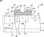
図2は、単位画素120Aの構成を示す図である。
FIG. 2 is a diagram illustrating a configuration of the
単位画素120Aは、光電変換素子として例えばフォトダイオード(PD)121を有している。フォトダイオード121は、例えば、N型基板131に形成されたP型ウェル層132に対して、P型層133(P+)を基板表面側に形成してN型埋め込み層134(N)を埋め込むことによって形成される埋め込み型フォトダイオードである。本実施の形態では、N型を第1の導電型、P型を第2の導電型とする。
The
単位画素120Aは、フォトダイオード121に加えて、第1転送ゲート122、メモリ部(MEM)123、第2転送ゲート124および浮遊拡散領域(FD:Floating Diffusion)125を有する。なお、単位画素120Aは、フォトダイオード121に光を導入する開口部や、各トランジスタのコンタクト部など以外の部分を遮光する遮光膜(図示せず)により遮光されている。
The unit pixel 120 </ b> A includes a
第1転送ゲート122は、フォトダイオード121で光電変換され、その内部に蓄積された電荷を、ゲート電極122Aに転送パルスTRXが印加されることによって転送する。また、第1転送ゲート122には、即ち、ゲート電極122Aの下で、かつ、フォトダイオード121とメモリ部123との境界部分には、N−の不純物拡散領域137を設けることによりオーバーフローパス130が形成される。さらに、不純物拡散領域137の直下には、不純物拡散領域137とは逆の導電型からなる濃いP+の不純物拡散領域138(P型ウェル層132よりも不純物濃度が高いP型の不純物層)が設けられている。なお、不純物拡散領域137および138については、図3および4を参照して後述する。
The
メモリ部123は、ゲート電極122Aの下に形成されたN型の埋め込みチャネル135(N)によって形成され、第1転送ゲート122によってフォトダイオード121から転送された電荷を保持する。メモリ部123が埋め込みチャネル135によって形成されていることで、基板界面での暗電流の発生を抑えることができるため画質の向上に寄与できる。
The
このメモリ部123において、その上部にゲート電極122Aを配置し、そのゲート電極122Aに転送パルスTRXを印加することでメモリ部123に変調をかけることができる。すなわち、ゲート電極122Aに転送パルスTRXが印加されることで、メモリ部123のポテンシャルが深くなる。これにより、メモリ部123の飽和電荷量を、変調を掛けない場合よりも増やすことができる。
In the
第2転送ゲート124は、メモリ部123に保持された電荷を、ゲート電極124Aに転送パルスTRGが印加されることによって転送する。浮遊拡散領域125は、N型層(N++)からなる電荷電圧変換部であり、第2転送ゲート124によってメモリ部123から転送された電荷を電圧に変換する。
The
単位画素120Aはさらに、リセットトランジスタ126、増幅トランジスタ127および選択トランジスタ128を有している。リセットトランジスタ126、増幅トランジスタ127および選択トランジスタ128は、図2の例では、NチャネルのMOSトランジスタを用いている。しかし、図2で例示したリセットトランジスタ126、増幅トランジスタ127および選択トランジスタ128の導電型の組み合わせは一例に過ぎず、これらの組み合わせに限られるものではない。
The
リセットトランジスタ126は、電源VDBと浮遊拡散領域125との間に接続されており、ゲート電極にリセットパルスRSTが印加されることによって浮遊拡散領域125をリセットする。増幅トランジスタ127は、ドレイン電極が電源VDOに接続され、ゲート電極が浮遊拡散領域125に接続されており、浮遊拡散領域125の電圧を読み出す。
The
選択トランジスタ128は、例えば、ドレイン電極が増幅トランジスタ127のソース電極に、ソース電極が垂直信号線117にそれぞれ接続されており、ゲート電極に選択パルスSELが印加されることで、画素信号を読み出すべき単位画素120Aを選択する。なお、選択トランジスタ128については、電源VDOと増幅トランジスタ127のドレイン電極との間に接続した構成を採ることも可能である。
In the
リセットトランジスタ126、増幅トランジスタ127および選択トランジスタ128については、その一つあるいは複数を画素信号の読み出し方法によって省略したり、複数の画素間で共有したりすることも可能である。
One or a plurality of the
単位画素120Aはさらに、フォトダイオード121の蓄積電荷を排出するための電荷排出部129を有している。この電荷排出部129は、露光開始時にゲート電極129Aに制御パルスABGが印加されることで、フォトダイオード121の電荷をN型層のドレイン部136(N++)に排出する。電荷排出部129はさらに、露光終了後の読み出し期間中にフォトダイオード121が飽和して電荷が溢れるのを防ぐ作用をなす。ドレイン部136には、所定の電圧VDAが印加されている。
The
[メモリ部123のゲート電極の電位]
ここで、電荷保持領域としてのメモリ部123のゲート電極、即ち、第1転送ゲート122のゲート電極122Aの電位について説明する。
[The potential of the gate electrode of the memory unit 123]
Here, the potential of the gate electrode of the
本実施形態においては、電荷保持領域としてのメモリ部123のゲート電極の電位が、第1転送ゲート122および第2転送ゲート124のうち少なくともいずれか、たとえば第1転送ゲート122を非導通状態とする期間に、ピニング状態とする電位に設定される。
より具体的には、第1転送ゲート122若しくは第2転送ゲート124のいずれか一方、または両方を非導通状態とする際に、ゲート電極122A,124Aに印加する電圧が、ゲート電極直下のSi表面に光電荷とは逆の極性のキャリアを蓄積できるピニング状態となるように設定される。
In the present embodiment, the potential of the gate electrode of the
More specifically, when one or both of the
本実施形態のように、転送ゲートを形成するトランジスタがN型の場合、第1転送ゲート122を非導通状態とする際に、ゲート電極122Aに印加する電圧がP型ウェル層132に対しグランドGNDよりも負電位となる電圧に設定される。なお、図示しないが、転送ゲートを形成するトランジスタがP型である場合、P型ウェル層がN型ウェル層となり、このN型ウェル層に対して電源電圧VDDよりも高い電圧に設定される。
As in this embodiment, when the transistor forming the transfer gate is N-type, when the
第1転送ゲート122を非導通状態とする際に、ゲート電極122Aに印加する電圧を、ゲート電極直下のSi表面に光電荷とは逆の極性のキャリアを蓄積できるピニング状態となるような電圧に設定する理由は以下の通りである。
When the
第1転送ゲート122のゲート電極122Aの電位を、P型ウェル層132に対して同電位(例えば0V)とすると、Si表面の結晶欠陥から発生するキャリアがメモリ部123に蓄積され、暗電流となり画質を劣化させるおそれがある。このため、本実施形態においては、メモリ部123上に形成されるゲート電極122Aのオフ(OFF)電位を、P型ウェル層132に対して負電位、例えば−2.0Vとする。これにより、本実施形態においては、電荷保持期間中はメモリ部123のSi表面に正孔(ホール:Hole)を発生させ、Si表面で発生した電子(エレクトロン:Electron)を再結合させることが可能で、その結果、暗電流を低減することが可能である。
When the potential of the
なお、図2の構成においては、メモリ部123の端部に、第2転送ゲート124のゲート電極124Aが存在することから、このゲート電極124Aも負電位とすることで、メモリ部123の端部で発生する暗電流を同様に抑えることが可能である。また、以下で説明する各実施の形態においては、N型基板を用いた構成例について説明しているが、P型基板を用いることも可能である。その場合、例えば図2に示した構成例では、N型基板131およびP型ウェル層132のいずれもP型半導体領域で形成される。
In the configuration of FIG. 2, since the
CMOSイメージセンサ100は、全画素同時に露光を開始し、全画素同時に露光を終了し、フォトダイオード121に蓄積された電荷を、遮光されたメモリ部123および浮遊拡散領域125へ順次転送することで、グローバル露光を実現する。このグローバル露光により、全画素一致した露光期間による歪みのない撮像が可能となる。
The CMOS image sensor 100 starts exposure of all pixels simultaneously, ends exposure of all pixels simultaneously, and sequentially transfers the charges accumulated in the
なお、本実施の形態での全画素とは、画像に現れる部分の画素の全てということであり、ダミー画素などは除外される。また、時間差や画像の歪みが問題にならない程度に十分小さければ、全画素同時の動作の代わりに複数行(例えば、数十行)ずつに高速に走査するものも含まれる。また、画像に表れる部分の画素の全てでなく、所定領域の複数行の画素に対してグローバル露光を行う場合でも本発明は適用可能である。 In addition, all the pixels in this Embodiment are all the pixels of the part which appears in an image, and a dummy pixel etc. are excluded. In addition, if the time difference and the distortion of the image are sufficiently small so as not to cause a problem, a method of scanning at a high speed for each of a plurality of lines (for example, several tens of lines) instead of the simultaneous operation of all the pixels is included. In addition, the present invention can be applied even when global exposure is performed on a plurality of rows of pixels in a predetermined area instead of all the pixels in the portion appearing in the image.
[第1の実施の形態]
次に、図3および図4を参照して、第1の実施の形態における単位画素120Aの構成について説明する。なお、図3および図4、並びに以下の図面では、図2の単位画素と共通する構成要素には同一の符号を付し、その詳細な説明は省略する。
[First Embodiment]
Next, the configuration of the
図3Aは、単位画素120Aの構成を示す平面図であり、図3Bは、図3Aの平面図に示されている矢印A−A’に沿った単位画素120Aの断面図である。
3A is a plan view showing the configuration of the
図3に示すように、単位画素120Aには、フォトダイオード121、メモリ部123、および浮遊拡散領域125が配置されている。フォトダイオード121およびメモリ部123は、電荷排出時に空乏状態となる不純物濃度で形成され、浮遊拡散領域125は、電圧を取り出すための配線コンタクトが電気的に接続できる不純物濃度で形成される。
As shown in FIG. 3, a
また、単位画素120Aでは、フォトダイオード121とメモリ部123との間に第1転送ゲート122が設けられ、メモリ部123と浮遊拡散領域125との間に第2転送ゲート124が設けられている。また、第1転送ゲート122およびメモリ部123を覆うようにゲート電極122Aが設けられ、第2転送ゲート124を覆うようにゲート電極124Aが設けられている。
In the unit pixel 120 </ b> A, a
そして、単位画素120Aでは、フォトダイオード121とメモリ部123との境界部分に形成されている第1転送ゲート122が設けられた領域に、所定量以上の信号電荷をフォトダイオード121からメモリ部123に自動的に排出するオーバーフローパス130が形成されている。ここで、第1転送ゲート122のゲート電極122Aには、ゲート電極122A下部のシリコン表面にホール(Hole)が蓄積するために必要な十分な負の電圧が印加されているものとする。
In the
図3Bに示すように、単位画素120Aでは、ゲート電極122Aの直下のフォトダイオード121とメモリ部123との境界部分の表面側に、フォトダイオード121およびメモリ部123を形成する不純物(N)と同一の導電型からなるN−の不純物拡散領域137を設けることによりオーバーフローパス130が形成されている。さらに、単位画素120Aでは、不純物拡散領域137の直下に、不純物拡散領域137とは逆の導電型からなる濃いP+の不純物拡散領域138が設けられている。
As shown in FIG. 3B, in the
より具体的には、N型基板131上にP型ウェル層132が形成され、フォトダイオード121は、HAD(Hole Accumulated Diode)構造からなるものとする。フォトダイオード121を構成するN型埋め込み層134の不純物濃度は、例えば、1016〜1018cm−3程度とし、フォトダイオード121の表面に形成されるP型層133の不純物濃度は、例えば、1017〜1018cm−3程度とする。また、メモリ部123を形成するN型の埋め込みチャネル135の不純物濃度は、フォトダイオード121のN型埋め込み層134と同様に、1016〜1018cm−3程度で形成される。
More specifically, a P-
そして、オーバーフローパス130を形成する不純物拡散領域137は、メモリ部123を形成するN型の埋め込みチャネル135よりも、接合深さは浅く、かつ、不純物濃度は低く設定される。また、オーバーフローパス130の下方に設けられる不純物拡散領域138は、フォトダイオード121およびメモリ部123が信号電荷を蓄積した状態において、フォトダイオード121およびメモリ部123のポテンシャルの侵入によって空乏状態とならない不純物濃度で形成される。例えば、不純物拡散領域138は、1017〜1018cm−3程度の不純物濃度で形成される。また、不純物拡散領域138の深さは、不純物拡散領域137の直下から、少なくともメモリ部123を形成するN型の埋め込みチャネル135の下端の深さまでとされる。
The
このように構成されているオーバーフローパス130のポテンシャル状態について、図4を参照して説明する。図4A乃至図4Cには、図3Bに示されている矢印Z1−Z1’に沿ったポテンシャル状態、矢印Z2−Z2’に沿ったポテンシャル状態、矢印C1−C1’に沿ったポテンシャル状態がそれぞれ示されている。
The potential state of the
図4Aに示すように、不純物拡散領域137が設けられた領域(フォトダイオード(PD)とメモリ部(MEM)の間の領域)ではポテンシャル障壁が低下している。また、図4Bに示すように、不純物拡散領域137の直下に設けられた不純物拡散領域138の領域では、非導通状態となるポテンシャル障壁となっている。
As shown in FIG. 4A, the potential barrier is lowered in the region where the
そして、オーバーフローパス130の深さ方向に沿った断面におけるポテンシャル状態は、図4Cに示すように、不純物拡散領域137において、電子に対してポテンシャル障壁の低い極小点が形成され、不純物拡散領域138において、電子に対してポテンシャル障壁の高い極大点が形成されている。
As shown in FIG. 4C, the potential state in the cross section along the depth direction of the
このように、不純物拡散領域138を設ける構成とすることでポテンシャルを高めることができるので、単位画素120Aのサイズを微細化することに伴ってオーバーフローパス130の転送経路が縮小されたとしても、フォトダイオード121からメモリ部123への所定量を超えた電荷のオーバーフローに必要なポテンシャル障壁を安定して形成することができるとともに、フォトダイオード121とメモリ部123との間のオーバーフローパス130下部の空乏層のつながりから発生するパンチスルー現象を防止することができる。
Since the potential can be increased by providing the
ここで、一般的にCMOSイメージセンサに代表される固体撮像素子では、光の吸収長というスケーリングされない物理定数が存在し、シリコン中の分光感度特性を維持させるためにはフォトダイオードのN型層の接合深さを浅くすることができないために、通常のMOSFETで用いられる定電界スケーリング則に従って、短チャネル効果を抑制しつつデザインルールを変更することは困難であった。これは、上述の特許文献1に開示されている構造でも同様であり、特に、メモリ部に保持可能な飽和電荷量を向上するために、浮遊拡散領域よりメモリ部のN型層の深さが深い場合には、微細化時において短チャネル効果によるパンチスルー現象が発生しやすい。また、フォトダイオードとメモリ部との間の水平方向の実効的な距離を延ばすことによって、短チャネル効果を回避することができると考えられるが、フォトダイオードおよびメモリ部における飽和電荷量を最大化するためには、その距離は狭く設計する必要がある。
Here, in a solid-state imaging device typically represented by a CMOS image sensor, there is an unscaled physical constant called light absorption length. In order to maintain the spectral sensitivity characteristics in silicon, the N-type layer of the photodiode Since the junction depth cannot be reduced, it is difficult to change the design rule while suppressing the short channel effect according to the constant field scaling law used in normal MOSFETs. This also applies to the structure disclosed in the above-mentioned
これに対し、単位画素120Aでは、フォトダイオード121とメモリ部123との間の水平方向の実効的な距離を増大させることなく、安定してオーバーフローパス130を形成することができる。これにより、フォトダイオード121において安定して所定の信号電荷を蓄積することができるので、撮像画像の画質が低下することが回避され、高画質な画像を取得することができる。
In contrast, in the
なお、図3の例では、N−の不純物拡散領域137を設けることによりオーバーフローパス130を形成した構造が採用されている。しかし、N−の不純物拡散領域137を設ける代わりに、P−の不純物拡散領域137を設けることによりオーバーフローパス130を形成した構造をとることも可能である。
In the example of FIG. 3, a structure in which an
[単位画素120Aの製造方法]
次に、図5を参照して、単位画素120Aの製造方法について説明する。
[Method of
Next, a manufacturing method of the
第1の工程において、P型ウェル層132が形成された基板表面に、第1転送ゲート122に対応する領域が開口するようなレジスト160−1が形成され、レジスト160−1を使用してP型のイオン注入が行われ、所定の深さとなる位置に不純物拡散領域138が形成される。
In the first step, a resist 160-1 having an opening corresponding to the
第2の工程において、レジスト160−1を使用してN型のイオン注入が行われ、不純物拡散領域138の上面から基板表面までの深さの領域に不純物拡散領域137が形成される。
In the second step, N-type ion implantation is performed using the resist 160-1 to form an
次に、レジスト160−1が除去された後、第3の工程において、メモリ部123に対応する領域が開口するようなレジスト160−2が形成され、レジスト160−2を使用してN型のイオン注入が行われ、埋め込みチャネル135が形成される。これにより、メモリ部123が形成される。
Next, after the resist 160-1 is removed, in a third step, a resist 160-2 is formed so as to open a region corresponding to the
次に、レジスト160−2が除去された後、第4の工程において、フォトダイオード121に対応する領域が開口するようなレジスト160−3が形成され、レジスト160−3を使用してN型のイオン注入が行われ、N型埋め込み層134が形成される。
Next, after the resist 160-2 is removed, in a fourth step, a resist 160-3 is formed so that a region corresponding to the
第5の工程において、レジスト160−3を使用してP型のイオン注入が行われ、N型埋め込み層134の表面にP型層133が形成され、これによりHAD型のフォトダイオード121が形成される。
In the fifth step, P-type ion implantation is performed using the resist 160-3, and a P-
第6の工程において、レジスト160−3を除去し、例えば、熱酸化法などによりゲート酸化膜を形成した後、ポリシリコンをCVD法によって堆積してゲート電極122Aが形成される。
In the sixth step, after removing the resist 160-3 and forming a gate oxide film by, eg, thermal oxidation, polysilicon is deposited by CVD to form the
以上のような工程を含むことで、単位画素120Aが製造される。なお、第4の工程において、N型埋め込み層134を形成する処理が行われる前に、ゲート電極122Aを形成する処理が行われてもよい。即ち、第6の工程を行ってゲート電極122Aが形成された後に、第4および第5の工程を行ってフォトダイオード121を形成することができる。
By including the steps as described above, the
[第2の実施の形態]
次に、図6は、第2の実施の形態における単位画素120Bの断面図である。
[Second Embodiment]
Next, FIG. 6 is a cross-sectional view of a
図6に示すように、単位画素120Bでは、オーバーフローパス130となる不純物拡散領域137の下部に形成される不純物拡散領域138Bが、メモリ部123を形成する埋め込みチャネル135の一部または全部の下側(基板の深い側)に延長するように形成されている。即ち、不純物拡散領域138Bは、図6に示す断面においてL字形状に形成されている。
As shown in FIG. 6, in the unit pixel 120 </ b> B, the
このように、不純物拡散領域138Bが埋め込みチャネル135の下側に延在することにより、メモリ部123の下部にも、N型埋め込み層134と埋め込みチャネル135との間と同様のポテンシャル障壁が形成される。これにより、単位画素120Bでは、N型埋め込み層134と埋め込みチャネル135との間で発生するパンチスルー現象を防止することができるとともに、メモリ部123の底部からフォトダイオード121に空乏層がつながってしまうことにより意図しない転送経路が形成されることを防止することができる。
As described above, the
さらに、単位画素120Bでは、メモリ部123よりも深い領域のP型ウェル層132に入射した光によって光電変換が行われることにより発生する電荷が、オーバーフローパス130を通過せずにメモリ部123に混入することを防止することができる。
Further, in the unit pixel 120 </ b> B, charges generated by photoelectric conversion by light incident on the P-
ここで、図7および図8を参照して、単位画素120Bにおける効果について、従来の構造の単位画素と比較して説明する。
Here, with reference to FIG. 7 and FIG. 8, the effect in the
図7Aには、第1転送ゲート122に不純物拡散領域137を設ける一方、不純物拡散領域138が設けられていない従来の構造(例えば、上述の特許文献1の図20と同様の構造)の単位画素のポテンシャル分布が示されている。図7Bには、図6の単位画素120Bのポテンシャル分布が示されている。また、フォトダイオード121およびメモリ部123は正の電位に設定され、第1転送ゲート122は負の電位に設定されているものとする。
FIG. 7A shows a unit pixel having a conventional structure (for example, a structure similar to FIG. 20 of
従来の構造の単位画素では、P型の不純物拡散領域137で構成されているオーバーフローパス130の下方の領域はP型ウェル層132のままであるため、その領域のポテンシャル障壁は、フォトダイオード121およびメモリ部123の影響を受けやすい構造となっている。即ち、図7Aのポテンシャル状態に示すように、フォトダイオード121とメモリ部123との境界にある0の等高線で囲まれた領域(オーバーフローパス130)の下部は、電子に対するポテンシャル障壁が低い。この結果、フォトダイオード121とメモリ部123との空乏層がつながりやすく、フォトダイオード121とメモリ部123との間の領域においてパンチスルー現象が発生しやすい。なお、オーバーフローパス130が、N型の不純物拡散領域で構成されていても同様である。
In the unit pixel having the conventional structure, since the region below the
これに対し、単位画素120Bでは、図7Bに示すように、オーバーフローパス130下部のポテンシャル障壁は、電子に対して高い値に固定されている。従って、単位画素120Bでは、フォトダイオード121およびメモリ部123からのポテンシャルの侵入を防止することができる。
On the other hand, in the
次に、図8には、図7Aに示した従来の構造の単位画素と、図7Bに示した単位画素120B(本発明の構造)とにおいて、オーバーフローパス130の転送経路長(Leff)を変化させた場合における閾値電圧(Vt)の変化をシミュレーションした結果が示されている。
Next, in FIG. 8, the transfer path length (Leff) of the
ここで、オーバーフローパス130の転送経路長は、図8の下側に示すように、フォトダイオード121とメモリ部123との間のオーバーフローパス130の長さである。また、閾値電圧は、フォトダイオード121とメモリ部123との間の閾値電圧を示す。図8において、y軸は、正方向に向かうに従い電子に対するポテンシャル障壁が低くなることを示し、負方向に向かうに従い電子に対するポテンシャル障壁が高くなることを示している。
Here, the transfer path length of the
図8に示すように、単位画素120B(本発明の構造)では、オーバーフローパス130下部のポテンシャルが変動し難く、短チャネル効果に強い構造になっている。また、転送経路長の変動(Δleff)に対する閾値変動(ΔVt)が抑制されていることが分かる。従って、単位画素120Bは、製造バラツキなどに起因した転送経路長の変動に対して頑健な構造である。
As shown in FIG. 8, the
[第3の実施の形態]
次に、図9は、第3の実施の形態における単位画素120Cの断面図である。
[Third Embodiment]
Next, FIG. 9 is a cross-sectional view of a unit pixel 120C in the third embodiment.
図9に示すように、単位画素120Cでは、オーバーフローパス130となる不純物拡散領域137の下部に形成される不純物拡散領域138Cは、図6の不純物拡散領域138Bと同様に、メモリ部123を形成する埋め込みチャネル135の下側に延在している。さらに、単位画素120Cでは、不純物拡散領域138Cの下側に、フォトダイオード121を形成するN型埋め込み層134Cが、不純物拡散領域138Cの下側に延長するように形成されている。即ち、不純物拡散領域138CおよびN型埋め込み層134Cが、図9に示す断面においてL字形状に形成されている。
As shown in FIG. 9, in the unit pixel 120C, the impurity diffusion region 138C formed below the
このように、N型埋め込み層134Cが埋め込みチャネル135の下側に延在することにより、オーバーフローパス130の形成を安定化することができる。さらに、メモリ部123よりも深い領域のP型ウェル層132に入射した光によって光電変換が行われることにより発生する電荷が、全てフォトダイオード121に集められるため、そのような電荷が、埋め込みチャネル135などのフォトダイオード121以外の領域に混入することを防止することができる。
Thus, the N-type buried layer 134C extends below the buried
[第4の実施の形態]
次に、図10は、第4の実施の形態における単位画素120Dの断面図である。
[Fourth Embodiment]
Next, FIG. 10 is a cross-sectional view of a
図10に示すように、単位画素120Dでは、フォトダイオード121を形成するN型埋め込み層134Dの一部が、第1転送ゲート122の下部に直接にオーバーラップする(平面的に見て重なり合う)ように形成されている。
As shown in FIG. 10, in the unit pixel 120 </ b> D, a part of the N-type buried
このようにN型埋め込み層134Dを形成することにより、フォトダイオード121に蓄積した信号電荷をメモリ部123に完全に転送する際に、その転送の動作に必要な第1転送ゲート122のゲート電極122Aに印加する電圧を低減させることができる。即ち、N型埋め込み層134Dは、第1転送ゲート122に対し、MOSトランジスタのソース領域に相当するので、N型埋め込み層134Dの一部が第1転送ゲート122にオーバーラップすることで、完全転送動作時における完全転送経路が形成されやすくなる。この結果、完全転送経路の形成に必要な電圧の低電圧化を図ることができる。
By forming the N-type buried layer 134D in this way, when the signal charge accumulated in the
[第5の実施の形態]
次に、図11は、第5の実施の形態における単位画素120Eの断面図である。
[Fifth Embodiment]
Next, FIG. 11 is a cross-sectional view of a
図11に示すように、単位画素120Eでは、メモリ部123を覆うゲート電極123Aが、オーバーフローパス130を覆うゲート電極122Aとは別に形成されている。ゲート電極123Aに転送パルスTRYが印加されることで、メモリ部123のポテンシャルが深くなる。さらに、ゲート電極123Aは、メモリ部123の遮光を担う材料として、例えば、タングステンなどの遮光性の高い金属によって形成されている。即ち、ゲート電極123Aは、メモリ部123に電荷を転送するための転送ゲートとしての機能と、メモリ部123を遮光するという機能とを兼ね備えている。
As shown in FIG. 11, in the
[第6の実施の形態]
次に、図12は、第6の実施の形態における単位画素120Fの断面図である。
[Sixth Embodiment]
Next, FIG. 12 is a sectional view of a
図12に示すように、単位画素120Fでは、メモリ部123の上部にゲート電極が設けられておらず、メモリ部123の不純物構造が、フォトダイオード121と同様にHAD構造となっている。即ち、単位画素120Fでは、メモリ部123が、P型ウェル層132中に形成されたN型の埋め込みチャネル135Aと、埋め込みチャネル135Aの表面側に形成されたP+のP型層135Bとにより構成されている。また、第1転送ゲート122のゲート電極122Aは、フォトダイオード121とメモリ部123との間の領域の表面に形成されている。
As shown in FIG. 12, in the unit pixel 120 </ b> F, the gate electrode is not provided on the upper portion of the
このように構成されている単位画素120Fでは、フォトダイオード121を形成するP型層133およびN型埋め込み層134、並びに、メモリ部123を構成する埋め込みチャネル135AおよびP型層135Bを、第1転送ゲート122のゲート電極122Aに対して自己整合的に形成することができる。
In the
[単位画素120Fの製造方法]
次に、図13を参照して、単位画素120Fの製造方法について説明する。
[Method of
Next, a manufacturing method of the
第1および第2の工程において、図5の製造方法と同様に、不純物拡散領域137および138が形成される。そして、第3の工程において、例えば、熱酸化法などによりゲート酸化膜を形成した後、ポリシリコンをCVD法によって堆積することにより、不純物拡散領域137の表面にゲート電極122Aが形成され、第1転送ゲート122が設けられる。
In the first and second steps,
第4の工程において、フォトダイオード121およびメモリ部123が形成される領域並びにゲート電極122A以外にレジスト160−2が形成され、レジスト160−2を使用してN型のイオン注入が行われる。これにより、埋め込みチャネル135Aと、N型埋め込み層134の一部となるN型埋め込み層134’が形成される。その後、レジスト160−2を使用してP型のイオン注入が行われることにより、P型層133およびP型層135Bが形成される。
In the fourth step, a resist 160-2 is formed in addition to the region where the
第5の工程において、P型層135Bを覆うようなレジスト160−3が形成され、レジスト160−3を使用してN型のイオン注入が行われる。これにより、N型埋め込み層134’の下部にN型の層が形成されて、N型埋め込み層134が形成される。なお、フォトダイオード121の深さをメモリ部123より深くする必要がなければ、第5の工程は省略することができる。
In the fifth step, a resist 160-3 that covers the P-
その後、第6の工程において、レジスト160−3が除去される。 Thereafter, in a sixth step, the resist 160-3 is removed.
以上のような工程を含むことで、単位画素120Fが製造される。この製造方法において、フォトダイオード121およびメモリ部123とゲート電極122Aとの境界は、フォトダイオード121およびメモリ部123を形成するためのイオン注入にゲート電極122Aがマスクとして使用されるため、ゲート電極122Aの端部に確実に一致する。即ち、フォトダイオード121およびメモリ部123は、ゲート電極122Aの端部に対して自己整合的に形成することができる。
By including the steps as described above, the
[第7の実施の形態]
次に、図14および図15を参照して、第7の実施の形態における単位画素120Gについて説明する。図14には、単位画素120Gの平面図が示されており、図15Aには、図14の平面図に示されている矢印A−A’に沿った断面図およびポテンシャル状態が示されており、図15Bには、図14の平面図に示されている矢印B−B’に沿った断面図およびポテンシャル状態が示されている。
[Seventh Embodiment]
Next, the
図14に示すように、単位画素120Gでは、オーバーフローパス130が、平面的に見て第1転送ゲート122の一部の領域に形成されている。即ち、単位画素120Gでは、フォトダイオード121に蓄積された所定電荷量を超える電荷をメモリ部123に転送する転送経路(オーバーフローパス130)と、フォトダイオード121に蓄積された全電荷をメモリ部123に完全に転送するための転送経路とが異なる領域に形成されている。
As shown in FIG. 14, in the
このようにオーバーフローパス130を第1転送ゲート122の一部の領域に形成する構成により、フォトダイオード121からメモリ部123にオーバーフローさせる電荷量を、オーバーフローパス130が形成される領域の幅(図14に示されている幅w)の設定によって調整することができる。
In this way, by forming the
なお、本実施の形態においては図示していないが、入射光のメモリ部123および浮遊拡散領域125への侵入を防止するために基板表面には遮光膜が配置されている。この遮光膜は、タングステンなどの材料により形成され、少なくともメモリ部123および浮遊拡散領域125の上部を覆うように設けられることが好ましい。
Although not shown in the present embodiment, a light-shielding film is disposed on the substrate surface in order to prevent incident light from entering the
なお、本実施の形態においては、電子を信号電荷とするイメージセンサを例に説明したが、正孔を信号電荷とするタイプのイメージセンサにも本発明を適用することができる。即ち、上述の各不純物層の導電型についてN型層とP型層とが反転して構成され、N型半導体層内にフォトダイオードおよびメモリ部がP型の不純物層で形成された場合であっても、上述の各構成においてオーバーフローパス130を形成する不純物拡散領域137の導電型としてN−またはP+をそれぞれ、P−またはN+と読み換えることによって、同様の効果を得ることができる。
In this embodiment, an image sensor using electrons as signal charges has been described as an example. However, the present invention can also be applied to an image sensor using holes as signal charges. That is, the N-type layer and the P-type layer are inverted with respect to the conductivity type of each impurity layer described above, and the photodiode and the memory portion are formed of the P-type impurity layer in the N-type semiconductor layer. However, the same effect can be obtained by replacing N− or P + with P− or N + as the conductivity type of the
また、上述したように不純物層の不純物濃度などについて数値を用いて説明したが、これらの数値は絶対的なものではなく、本発明の技術的思想について理解を助けるために設定したものに過ぎない。即ち、本発明の範疇は、上述の説明で用いた数値に限定されず設定することができるものである。 Further, as described above, the impurity concentration of the impurity layer has been described using numerical values, but these numerical values are not absolute values, and are merely set to help understanding the technical idea of the present invention. . That is, the category of the present invention can be set without being limited to the numerical values used in the above description.
なお、各実施の形態においては、電子を信号電荷とするイメージセンサを例に説明したが、正孔を信号電荷とするタイプのイメージセンサにも本発明を適用することができる。 In each embodiment, the image sensor using electrons as signal charges has been described as an example. However, the present invention can also be applied to an image sensor using holes as signal charges.
[単位画素のその他の第1構成例]
図16は、単位画素120のその他の第1構成例である単位画素120H−1の構造を示す図である。
[Other First Configuration Example of Unit Pixel]
FIG. 16 is a diagram illustrating a structure of a unit pixel 120H-1, which is another first configuration example of the unit pixel 120.
単位画素120H−1では、図2の単位画素120Aにおける第1転送ゲート122とメモリ部123が省略され、P型ウェル層132を挟んで、フォトダイオード121と浮遊拡散領域125が隣接する配置となっている。フォトダイオード121と浮遊拡散領域125の間のP型ウェル層132の上側には、第2転送ゲート124が配置されている。
In the unit pixel 120H-1, the
単位画素120H−1におけるグローバル露光動作について説明する。まず、全画素同時に埋め込みフォトダイオード121の蓄積電荷を空にする電荷排出動作が実行された後、露光が開始される。これにより、フォトダイオード121のPN接合容量に光電荷が蓄積される。露光期間終了時点で、第2転送ゲート124が全画素同時にONされ、蓄積された光電荷が全て浮遊拡散領域125へと転送される。第2転送ゲート124を閉じることで、全画素同一の露光期間で蓄積された光電荷が浮遊拡散領域125で保持される。その後、浮遊拡散領域125で保持された光電荷が、順次、画素信号として垂直信号線117を通して読み出される。最後に、浮遊拡散領域125がリセットされ、しかる後、リセットレベルが読み出される。
A global exposure operation in the unit pixel 120H-1 will be described. First, after a charge discharging operation for emptying the charge stored in the embedded
従って、単位画素120H−1では、浮遊拡散領域125がグローバル露光動作を行う場合の電荷保持領域となる。単位画素120H−1では、フォトダイオード121と浮遊拡散領域125との境界部分の第2転送ゲート124に、不純物拡散領域137を形成することによりオーバーフローパス130を設けるとともに、不純物拡散領域137の直下に不純物拡散領域138を設けることで、本発明を適用できる。
Therefore, in the unit pixel 120H-1, the floating
[単位画素のその他の第2構成例]
図17は、単位画素120のその他の第2構成例である単位画素120H−2の構造を示す図である。
[Other Second Configuration Example of Unit Pixel]
FIG. 17 is a diagram illustrating a structure of a unit pixel 120H-2 that is another second configuration example of the unit pixel 120. As illustrated in FIG.
単位画素120H−2は、図2の単位画素120Aの構成に、浮遊拡散領域125と同様のメモリ部123が設けられた構成となっている。即ち、単位画素120H−2では、第1転送ゲート122のゲート電極122Aがフォトダイオード121とメモリ部123の境界のP型ウェル層132の上部に設けられている。また、単位画素120H−2では、メモリ部123が浮遊拡散領域125と同様のN型層138によって形成される。
The unit pixel 120H-2 has a configuration in which a
単位画素120H−2におけるグローバル露光動作は、次の手順で実行される。まず、電荷排出動作が全画素同時に実行され、同時露光が開始される。発生した光電荷がフォトダイオード121に蓄積される。露光終了時点で、第1転送ゲート122が全画素同時にONされ、蓄積された光電荷がメモリ部123へ転送され、保持される。露光終了後、順次動作にてリセットレベルと信号レベルが読み出される。即ち、浮遊拡散領域125がリセットされ、次にリセットレベルが読み出される。続いて、メモリ部123の保持電荷が浮遊拡散領域125へ転送され、信号レベルが読み出される。
The global exposure operation in the unit pixel 120H-2 is executed according to the following procedure. First, the charge discharging operation is executed simultaneously for all pixels, and simultaneous exposure is started. The generated photocharge is accumulated in the
単位画素120H−2では、メモリ部123のN型層138がグローバル露光動作を行う場合の電荷保持領域となる。単位画素120H−2では、第1転送ゲート122に、不純物拡散領域137を形成することによりオーバーフローパス130を設けるとともに、不純物拡散領域137の直下に不純物拡散領域138を設けることで、本発明を適用できる。
In the unit pixel 120H-2, the N-
[単位画素のその他の第3構成例]
図18は、単位画素120のその他の第3構成例である単位画素120H−3の構造を示す図である。
[Other Third Configuration Example of Unit Pixel]
FIG. 18 is a diagram illustrating a structure of a unit pixel 120H-3 as another third configuration example of the unit pixel 120.
図2の単位画素120Aでは、フォトダイオード121と浮遊拡散領域125の間に1つのメモリ部(MEM)123が配置されていたが、図18の単位画素120H−3では、さらにもう1つのメモリ部(MEM2)142が配置されている。即ち、メモリ部が2段構成となっている。
In the
第3転送ゲート141は、メモリ部123に蓄積された電荷を、ゲート電極141Aに転送パルスTRX2が印加されることによって転送する。メモリ部142は、ゲート電極141Aの下に形成されたN型の埋め込みチャネル143によって形成され、第3転送ゲート141によってメモリ部123から転送された電荷を蓄積する。メモリ部142が埋め込みチャネル143によって形成されていることで、界面での暗電流の発生を抑えることができるため画質の向上に寄与できる。
The
メモリ部142は、メモリ部123と同様の構成とされているので、メモリ部123と同様、変調を掛けた場合には、メモリ部142の飽和電荷量を変調を掛けない場合よりも増やすことができる。
Since the
単位画素120H−3におけるグローバル露光動作では、全画素同時に蓄積された光電荷はフォトダイオード121またはメモリ部123で保持される。メモリ部142は、画素信号が読み出されるまでの間、光電荷を保持するために使用される。
In the global exposure operation in the unit pixel 120 </ b> H- 3, the photocharge accumulated simultaneously in all the pixels is held in the
単位画素120H−3では、メモリ部123の埋め込みチャネル135およびメモリ部142の埋め込みチャネル143がグローバル露光動作を行う場合の電荷保持領域となる。単位画素120H−3では、第1転送ゲート122に、不純物拡散領域137を形成することによりオーバーフローパス130を設けるとともに、不純物拡散領域137の直下に不純物拡散領域138を設けることで、本発明を適用できる。
In the unit pixel 120H-3, the embedded
以上のように、本発明は、単位画素120A以外のその他の構造にも採用することができる。また、単位画素120A乃至120H−3において、導電型の極性(N型、P型)を反対にしたものでも同様に適用可能である。
As described above, the present invention can be applied to other structures other than the
[本発明を適用した電子機器の構成例]
さらに本発明は、固体撮像素子への適用に限られるものではない。即ち、本発明は、デジタルスチルカメラやビデオカメラ等の撮像装置や、撮像機能を有する携帯端末装置や、画像読取部に固体撮像素子を用いる複写機など、画像取込部(光電変換部)に固体撮像素子を用いる電子機器全般に対して適用可能である。固体撮像素子は、ワンチップとして形成された形態であってもよいし、撮像部と信号処理部または光学系とがまとめてパッケージングされた撮像機能を有するモジュール状の形態であってもよい。
[Configuration Example of Electronic Device to which the Present Invention is Applied]
Furthermore, the present invention is not limited to application to a solid-state imaging device. That is, the present invention is applied to an image capturing unit (photoelectric conversion unit) such as an imaging device such as a digital still camera or a video camera, a portable terminal device having an imaging function, or a copying machine using a solid-state imaging device as an image reading unit. The present invention can be applied to all electronic devices using a solid-state image sensor. The solid-state imaging device may be formed as a one-chip, or may be in a module shape having an imaging function in which an imaging unit and a signal processing unit or an optical system are packaged together.
図19は、本発明を適用した電子機器としての、撮像装置の構成例を示すブロック図である。 FIG. 19 is a block diagram illustrating a configuration example of an imaging apparatus as an electronic apparatus to which the present invention is applied.
図19の撮像装置300は、レンズ群などからなる光学部301、上述した単位画素120の各構成が採用される固体撮像素子(撮像デバイス)302、およびカメラ信号処理回路であるDSP(Digital Signal Processor)回路303を備える。また、撮像装置300は、フレームメモリ304、表示部305、記録部306、操作部307、および電源部308も備える。DSP回路303、フレームメモリ304、表示部305、記録部306、操作部307および電源部308は、バスライン309を介して相互に接続されている。
An imaging apparatus 300 in FIG. 19 includes an
光学部301は、被写体からの入射光(像光)を取り込んで固体撮像素子302の撮像面上に結像する。固体撮像素子302は、光学部301によって撮像面上に結像された入射光の光量を画素単位で電気信号に変換して画素信号として出力する。この固体撮像素子302として、CMOSイメージセンサ100の固体撮像素子、即ちグローバル露光によって歪みのない撮像を実現できるとともに、RGBの画素ごとの漏れ込み信号抑圧比を抑制することができる固体撮像素子を用いることができる。
The
表示部305は、例えば、液晶パネルや有機EL(Electro Luminescence)パネル等のパネル型表示装置からなり、固体撮像素子302で撮像された動画または静止画を表示する。記録部306は、固体撮像素子302で撮像された動画または静止画を、ビデオテープやDVD(Digital Versatile Disk)等の記録媒体に記録する。
The
操作部307は、ユーザによる操作の下に、撮像装置300が持つ様々な機能について操作指令を発する。電源部308は、DSP回路303、フレームメモリ304、表示部305、記録部306および操作部307の動作電源となる各種の電源を、これら供給対象に対して適宜供給する。
The
上述したように、固体撮像素子302として、上述した実施の形態に係るCMOSイメージセンサ100を用いることで、グローバル露光によって歪みのない撮像を実現できるとともに、RGBの画素ごとの漏れ込み信号抑圧比を抑制することができる。従って、ビデオカメラやデジタルスチルカメラ、さらには携帯電話機等のモバイル機器向けカメラモジュールなどの撮像装置300においても、撮像画像の高画質化を図ることができる。
As described above, by using the CMOS image sensor 100 according to the above-described embodiment as the solid-
また、上述した実施形態においては、可視光の光量に応じた信号電荷を物理量として検知する単位画素が行列状に配置されてなるCMOSイメージセンサに適用した場合を例に挙げて説明した。しかしながら、本発明はCMOSイメージセンサへの適用に限られるものではなく、画素アレイ部の画素列ごとにカラム処理部を配置してなるカラム方式の固体撮像素子全般に対して適用可能である。 In the above-described embodiment, the case where the present invention is applied to a CMOS image sensor in which unit pixels that detect signal charges corresponding to the amount of visible light as physical quantities are arranged in a matrix has been described as an example. However, the present invention is not limited to application to a CMOS image sensor, and can be applied to all column-type solid-state imaging devices in which a column processing unit is arranged for each pixel column of a pixel array unit.
また、本発明は、可視光の入射光量の分布を検知して画像として撮像する固体撮像素子への適用に限らず、赤外線やX線、あるいは粒子等の入射量の分布を画像として撮像する固体撮像素子や、広義の意味として、圧力や静電容量など、他の物理量の分布を検知して画像として撮像する指紋検出センサ等の固体撮像素子(物理量分布検知装置)全般に対して適用可能である。 Further, the present invention is not limited to application to a solid-state imaging device that detects the distribution of the amount of incident light of visible light and captures it as an image, but a solid that captures the distribution of the incident amount of infrared rays, X-rays, or particles as an image Applicable to imaging devices and, in a broad sense, solid-state imaging devices (physical quantity distribution detection devices) such as fingerprint detection sensors that detect the distribution of other physical quantities such as pressure and capacitance and capture images as images. is there.
なお、固体撮像装置はワンチップとして形成された形態であってもよいし、撮像部と、信号処理部または光学系とがまとめてパッケージングされた撮像機能を有するモジュール状の形態であってもよい。 The solid-state imaging device may be formed as a single chip, or may be in a module-like form having an imaging function in which an imaging unit and a signal processing unit or an optical system are packaged together. Good.
本発明の実施の形態は、上述した実施の形態に限定されるものではなく、本発明の要旨を逸脱しない範囲において種々の変更が可能である。 The embodiments of the present invention are not limited to the above-described embodiments, and various modifications can be made without departing from the scope of the present invention.
100 CMOSイメージセンサ, 111 画素アレイ部, 120 単位画素, 121 フォトダイオード, 123 メモリ部, 132 P型ウェル層, 134 N型埋め込み層, 122 第1転送ゲート, 135 埋め込みチャネル, 300 撮像装置 100 CMOS image sensor, 111 pixel array unit, 120 unit pixel, 121 photodiode, 123 memory unit, 132 P-type well layer, 134 N-type buried layer, 122 first transfer gate, 135 buried channel, 300 imaging device
Claims (12)
第1の導電型の不純物領域からなり、入射光量に応じた電荷を発生して内部に蓄積する光電変換素子と、
前記第1の導電型の不純物領域からなり、前記光電変換素子によって変換された電荷を読み出されるまで保持する電荷保持領域と、
前記光電変換素子と前記電荷保持領域との間の領域に配置される第1の導電型の不純物領域からなり、露光期間中において前記光電変換素子で発生した所定電荷量を超える電荷だけを前記電荷保持領域に転送する中間転送経路と、
前記光電変換素子と前記電荷保持領域との間の領域であって、かつ、前記中間転送経路の下部の領域に配置され、前記第2の導電型による半導体領域よりも不純物濃度が高い第2の導電型の不純物領域からなる不純物層と
を備える固体撮像素子。 A semiconductor region of a second conductivity type formed on the surface side of the semiconductor substrate;
A photoelectric conversion element comprising an impurity region of a first conductivity type, generating a charge corresponding to the amount of incident light and storing it inside;
A charge holding region comprising the impurity region of the first conductivity type and holding the charge converted by the photoelectric conversion element until it is read;
The first conductive type impurity region is disposed in a region between the photoelectric conversion element and the charge holding region, and only charges exceeding a predetermined charge amount generated in the photoelectric conversion element during an exposure period are included in the charge. An intermediate transfer path to transfer to the holding area;
A second region having a higher impurity concentration than the semiconductor region of the second conductivity type, which is disposed between the photoelectric conversion element and the charge holding region and in a lower region of the intermediate transfer path. A solid-state imaging device comprising: an impurity layer comprising a conductive impurity region.
請求項1に記載の固体撮像素子。 The junction depth of the impurity region of the first conductivity type forming the intermediate transfer path is shallower than the junction depth of the impurity region of the first conductivity type forming the charge holding region, and the intermediate transfer The impurity concentration of the impurity region of the first conductivity type that forms a path is set lower than the impurity concentration of the impurity region of the first conductivity type that forms the charge retention region. Solid-state image sensor.
請求項1に記載の固体撮像素子。 The solid-state imaging device according to claim 1, wherein the impurity layer including the impurity region of the second conductivity type is formed with a predetermined impurity concentration that is not depleted by a potential of the photoelectric conversion element and the charge holding region.
請求項1に記載の固体撮像素子。 The potential state along the depth direction passing through the intermediate transfer path is at least a potential minimum point and a potential maximum point at a position shallower than the lower end of the impurity region of the first conductivity type forming the charge retention region. The solid-state imaging device according to claim 1, wherein one or more are formed, and the potential maximum point is formed at a position deeper than the potential minimum point.
請求項1に記載の固体撮像素子。 The solid-state imaging device according to claim 1, wherein the impurity layer including the impurity region of the second conductivity type is formed to a depth at a lower end of the impurity region of the first conductivity type that forms the charge holding region.
請求項1に記載の固体撮像素子。 The impurity layer including the impurity region of the second conductivity type has the first conductivity type of the first conductivity type that forms the charge holding region from directly below the impurity region of the first conductivity type that forms the intermediate transfer path. The solid-state imaging element according to claim 1, wherein the solid-state imaging element is formed in a shape extending toward a lower portion of the impurity region.
請求項6に記載の固体撮像素子。 The impurity region of the first conductivity type that forms the photoelectric conversion element is located immediately below the impurity layer formed on the surface of the impurity region, from the impurity region of the first conductivity type that forms the charge holding region. The solid-state imaging element according to claim 6, wherein the solid-state imaging element is formed in a shape extending toward a lower portion of the impurity layer including the impurity region of the second conductivity type extending toward a lower portion.
前記光電変換素子を形成する第1の導電型の前記不純物領域が形成された領域と、前記転送ゲートとが、平面的に見て互いに重なり合うように配置される
請求項1に記載の固体撮像素子。 Provided above the intermediate transfer path and the charge holding region, further comprising a transfer gate for transferring charges from the photoelectric conversion region to the charge holding region;
2. The solid-state imaging device according to claim 1, wherein a region in which the impurity region of the first conductivity type forming the photoelectric conversion device is formed and the transfer gate are arranged so as to overlap each other when seen in a plan view. .
請求項1に記載の固体撮像素子。 The solid-state imaging device according to claim 1, wherein the photoelectric conversion element and the charge holding region are configured by a HAD (Hole Accumulated Diode) structure.
前記電荷保持領域の上部を覆う第2の電極と
をさらに備え、
前記第1の電極と前記第2の電極とが分離して形成されている
請求項1に記載の固体撮像素子。 A first electrode covering an upper portion of the intermediate transfer path;
A second electrode covering an upper portion of the charge retention region;
The solid-state imaging device according to claim 1, wherein the first electrode and the second electrode are formed separately.
前記第1の導電型の不純物領域からなり、前記光電変換素子によって変換された電荷を読み出されるまで保持する電荷保持領域を形成し、
前記光電変換素子と前記電荷保持領域との間の領域に配置される第1の導電型の不純物領域からなり、露光期間中において前記光電変換素子で発生した所定電荷量を超える電荷だけを前記電荷保持領域に転送する中間転送経路を形成し、
前記光電変換素子と前記電荷保持領域との間の領域であって、かつ、前記中間転送経路の下部の領域に配置され、半導体基板の表面側に形成される前記第2の導電型による半導体領域よりも不純物濃度が高い第2の導電型の不純物領域からなる不純物層を形成する
ステップを含む固体撮像素子の製造方法。 Forming a photoelectric conversion element comprising an impurity region of the first conductivity type, generating a charge corresponding to the amount of incident light and storing it inside;
Forming a charge holding region comprising the impurity region of the first conductivity type and holding the charge converted by the photoelectric conversion element until it is read;
The first conductive type impurity region is disposed in a region between the photoelectric conversion element and the charge holding region, and only charges exceeding a predetermined charge amount generated in the photoelectric conversion element during an exposure period are included in the charge. Form an intermediate transfer path to transfer to the holding area,
A semiconductor region of the second conductivity type, which is located between the photoelectric conversion element and the charge holding region, and is disposed in a lower region of the intermediate transfer path and formed on the surface side of the semiconductor substrate A method for manufacturing a solid-state imaging device, including the step of forming an impurity layer made of an impurity region of a second conductivity type having a higher impurity concentration.
第1の導電型の不純物領域からなり、入射光量に応じた電荷を発生して内部に蓄積する光電変換素子と、
前記第1の導電型の不純物領域からなり、前記光電変換素子によって変換された電荷を読み出されるまで保持する電荷保持領域と、
前記光電変換素子と前記電荷保持領域との間の領域に配置される第1の導電型の不純物領域からなり、露光期間中において前記光電変換素子で発生した所定電荷量を超える電荷だけを前記電荷保持領域に転送する中間転送経路と、
前記光電変換素子と前記電荷保持領域との間の領域であって、かつ、前記中間転送経路の下部の領域に配置され、前記第2の導電型による半導体領域よりも不純物濃度が高い第2の導電型の不純物領域からなる不純物層と
を備える固体撮像素子を有し、
行列状に配置された複数行の単位画素が同時に前記電荷の蓄積を行い、
前記光電変換素子から前記電荷保持領域に転送された前記電荷を順次読み出す
電子機器。 A semiconductor region of a second conductivity type formed on the surface side of the semiconductor substrate;
A photoelectric conversion element comprising an impurity region of a first conductivity type, generating a charge corresponding to the amount of incident light and storing it inside;
A charge holding region comprising the impurity region of the first conductivity type and holding the charge converted by the photoelectric conversion element until it is read;
The first conductive type impurity region is disposed in a region between the photoelectric conversion element and the charge holding region, and only charges exceeding a predetermined charge amount generated in the photoelectric conversion element during an exposure period are included in the charge. An intermediate transfer path to transfer to the holding area;
A second region having a higher impurity concentration than the semiconductor region of the second conductivity type, which is disposed between the photoelectric conversion element and the charge holding region and in a lower region of the intermediate transfer path. And a solid-state imaging device including an impurity layer made of a conductive impurity region,
A plurality of rows of unit pixels arranged in a matrix simultaneously accumulate the charges,
An electronic device that sequentially reads out the charges transferred from the photoelectric conversion element to the charge holding region.
Priority Applications (3)
| Application Number | Priority Date | Filing Date | Title |
|---|---|---|---|
| JP2010083600A JP2011216673A (en) | 2010-03-31 | 2010-03-31 | Solid-state imaging device, method for manufacturing of solid-state imaging device, and electronic apparatus |
| US13/053,455 US8629484B2 (en) | 2010-03-31 | 2011-03-22 | Solid-state imaging device, method of manufacturing solid-state imaging device, and electronic apparatus |
| CN201110075913.6A CN102208423B (en) | 2010-03-31 | 2011-03-24 | Solid camera head, the method manufacturing solid camera head and electronic equipment |
Applications Claiming Priority (1)
| Application Number | Priority Date | Filing Date | Title |
|---|---|---|---|
| JP2010083600A JP2011216673A (en) | 2010-03-31 | 2010-03-31 | Solid-state imaging device, method for manufacturing of solid-state imaging device, and electronic apparatus |
Publications (2)
| Publication Number | Publication Date |
|---|---|
| JP2011216673A true JP2011216673A (en) | 2011-10-27 |
| JP2011216673A5 JP2011216673A5 (en) | 2013-05-09 |
Family
ID=44697173
Family Applications (1)
| Application Number | Title | Priority Date | Filing Date |
|---|---|---|---|
| JP2010083600A Ceased JP2011216673A (en) | 2010-03-31 | 2010-03-31 | Solid-state imaging device, method for manufacturing of solid-state imaging device, and electronic apparatus |
Country Status (3)
| Country | Link |
|---|---|
| US (1) | US8629484B2 (en) |
| JP (1) | JP2011216673A (en) |
| CN (1) | CN102208423B (en) |
Cited By (12)
| Publication number | Priority date | Publication date | Assignee | Title |
|---|---|---|---|---|
| JP2011249406A (en) * | 2010-05-24 | 2011-12-08 | Brookman Technology Inc | Solid-state imaging apparatus |
| JP2015026696A (en) * | 2013-07-25 | 2015-02-05 | キヤノン株式会社 | Photoelectric conversion device and imaging system |
| JP2015065271A (en) * | 2013-09-25 | 2015-04-09 | ソニー株式会社 | Solid state imaging device and an operating method thereof, electronic apparatus and operating method thereof |
| JP2015220279A (en) * | 2014-05-15 | 2015-12-07 | キヤノン株式会社 | Imaging device |
| JP2016516294A (en) * | 2013-03-06 | 2016-06-02 | アップル インコーポレイテッド | Charge transfer in image sensors |
| JP2016111224A (en) * | 2014-12-08 | 2016-06-20 | 株式会社ブルックマンテクノロジ | Photodetector and solid state image sensor |
| WO2016152184A1 (en) * | 2015-03-25 | 2016-09-29 | ソニー株式会社 | Solid-state imaging device and method for driving solid-state imaging device |
| JP2018120981A (en) * | 2017-01-26 | 2018-08-02 | キヤノン株式会社 | Solid state image sensor, imaging system, and manufacturing method of solid state image sensor |
| JP2019009155A (en) * | 2017-06-20 | 2019-01-17 | キヤノン株式会社 | Imaging device, imaging system, mobile body, and method of manufacturing imaging device |
| JP2019117949A (en) * | 2019-04-08 | 2019-07-18 | 浜松ホトニクス株式会社 | Solid-state imaging apparatus |
| KR20190086660A (en) * | 2016-12-01 | 2019-07-23 | 소니 세미컨덕터 솔루션즈 가부시키가이샤 | Solid-state imaging device, method of manufacturing solid-state imaging device, and imaging device |
| WO2020050007A1 (en) * | 2018-09-07 | 2020-03-12 | ソニーセミコンダクタソリューションズ株式会社 | Solid state imaging device and electronic apparatus |
Families Citing this family (42)
| Publication number | Priority date | Publication date | Assignee | Title |
|---|---|---|---|---|
| JP5671830B2 (en) * | 2010-03-31 | 2015-02-18 | ソニー株式会社 | Solid-state imaging device, manufacturing method of solid-state imaging device, and electronic apparatus |
| JP5637384B2 (en) * | 2010-12-15 | 2014-12-10 | ソニー株式会社 | Solid-state imaging device, driving method, and electronic apparatus |
| JP6004665B2 (en) * | 2012-02-17 | 2016-10-12 | キヤノン株式会社 | Imaging device and imaging system. |
| JP6012197B2 (en) * | 2012-02-17 | 2016-10-25 | キヤノン株式会社 | Imaging device and driving method of imaging device |
| KR20130106978A (en) * | 2012-03-21 | 2013-10-01 | 삼성전자주식회사 | Unit pixel of image sensor and image sensor including the same |
| JP2014011253A (en) * | 2012-06-28 | 2014-01-20 | Sony Corp | Solid state image pickup device and electronic apparatus |
| US9293500B2 (en) | 2013-03-01 | 2016-03-22 | Apple Inc. | Exposure control for image sensors |
| US9276031B2 (en) | 2013-03-04 | 2016-03-01 | Apple Inc. | Photodiode with different electric potential regions for image sensors |
| US9041837B2 (en) | 2013-03-05 | 2015-05-26 | Apple Inc. | Image sensor with reduced blooming |
| US9549099B2 (en) | 2013-03-12 | 2017-01-17 | Apple Inc. | Hybrid image sensor |
| US9319611B2 (en) | 2013-03-14 | 2016-04-19 | Apple Inc. | Image sensor with flexible pixel summing |
| JP2015095468A (en) * | 2013-11-08 | 2015-05-18 | ソニー株式会社 | Solid state imaging element, method for manufacturing solid state imaging element, and electronic apparatus |
| US9596423B1 (en) | 2013-11-21 | 2017-03-14 | Apple Inc. | Charge summing in an image sensor |
| US9596420B2 (en) | 2013-12-05 | 2017-03-14 | Apple Inc. | Image sensor having pixels with different integration periods |
| US9473706B2 (en) | 2013-12-09 | 2016-10-18 | Apple Inc. | Image sensor flicker detection |
| US10285626B1 (en) | 2014-02-14 | 2019-05-14 | Apple Inc. | Activity identification using an optical heart rate monitor |
| US9232150B2 (en) | 2014-03-12 | 2016-01-05 | Apple Inc. | System and method for estimating an ambient light condition using an image sensor |
| US9277144B2 (en) | 2014-03-12 | 2016-03-01 | Apple Inc. | System and method for estimating an ambient light condition using an image sensor and field-of-view compensation |
| US9584743B1 (en) | 2014-03-13 | 2017-02-28 | Apple Inc. | Image sensor with auto-focus and pixel cross-talk compensation |
| US9497397B1 (en) | 2014-04-08 | 2016-11-15 | Apple Inc. | Image sensor with auto-focus and color ratio cross-talk comparison |
| US9538106B2 (en) | 2014-04-25 | 2017-01-03 | Apple Inc. | Image sensor having a uniform digital power signature |
| US9686485B2 (en) | 2014-05-30 | 2017-06-20 | Apple Inc. | Pixel binning in an image sensor |
| JP2017054947A (en) * | 2015-09-10 | 2017-03-16 | セイコーエプソン株式会社 | Solid-state image sensor and method for manufacturing the same, and electronic apparatus |
| JP2017143189A (en) * | 2016-02-10 | 2017-08-17 | ルネサスエレクトロニクス株式会社 | Solid-state imaging device |
| US9912883B1 (en) | 2016-05-10 | 2018-03-06 | Apple Inc. | Image sensor with calibrated column analog-to-digital converters |
| US10438987B2 (en) | 2016-09-23 | 2019-10-08 | Apple Inc. | Stacked backside illuminated SPAD array |
| WO2018140522A2 (en) | 2017-01-25 | 2018-08-02 | Apple Inc. | Spad detector having modulated sensitivity |
| US10656251B1 (en) | 2017-01-25 | 2020-05-19 | Apple Inc. | Signal acquisition in a SPAD detector |
| US10962628B1 (en) | 2017-01-26 | 2021-03-30 | Apple Inc. | Spatial temporal weighting in a SPAD detector |
| WO2018193747A1 (en) * | 2017-04-19 | 2018-10-25 | Sony Semiconductor Solutions Corporation | Semiconductor device, method of manufacturing the same, and electronic apparatus |
| US10622538B2 (en) | 2017-07-18 | 2020-04-14 | Apple Inc. | Techniques for providing a haptic output and sensing a haptic input using a piezoelectric body |
| US10440301B2 (en) | 2017-09-08 | 2019-10-08 | Apple Inc. | Image capture device, pixel, and method providing improved phase detection auto-focus performance |
| CN110098203A (en) * | 2018-01-30 | 2019-08-06 | 维深半导体公司 | Back side illumination image sensor and its preparation |
| US10559614B2 (en) * | 2018-03-09 | 2020-02-11 | Semiconductor Components Industries, Llc | Dual conversion gain circuitry with buried channels |
| US11019294B2 (en) | 2018-07-18 | 2021-05-25 | Apple Inc. | Seamless readout mode transitions in image sensors |
| US10848693B2 (en) | 2018-07-18 | 2020-11-24 | Apple Inc. | Image flare detection using asymmetric pixels |
| US11233966B1 (en) | 2018-11-29 | 2022-01-25 | Apple Inc. | Breakdown voltage monitoring for avalanche diodes |
| TWI685959B (en) * | 2019-01-07 | 2020-02-21 | 力晶積成電子製造股份有限公司 | Image sensor and manufacturing method therefore |
| US11503234B2 (en) * | 2019-02-27 | 2022-11-15 | Canon Kabushiki Kaisha | Photoelectric conversion device, imaging system, radioactive ray imaging system, and movable object |
| KR20210133739A (en) * | 2020-04-29 | 2021-11-08 | 에스케이하이닉스 주식회사 | Image Sensor |
| US11563910B2 (en) | 2020-08-04 | 2023-01-24 | Apple Inc. | Image capture devices having phase detection auto-focus pixels |
| US11546532B1 (en) | 2021-03-16 | 2023-01-03 | Apple Inc. | Dynamic correlated double sampling for noise rejection in image sensors |
Citations (6)
| Publication number | Priority date | Publication date | Assignee | Title |
|---|---|---|---|---|
| JP2005347758A (en) * | 2004-06-04 | 2005-12-15 | Samsung Electronics Co Ltd | Cmos image sensor and manufacturing method therefor |
| JP2008004692A (en) * | 2006-06-21 | 2008-01-10 | Nikon Corp | Solid-state imaging device |
| JP2008103647A (en) * | 2006-10-20 | 2008-05-01 | National Univ Corp Shizuoka Univ | Semiconductor element and solid state imaging device |
| JP2009253149A (en) * | 2008-04-09 | 2009-10-29 | Canon Inc | Photoelectric conversion device and imaging system using same |
| JP2009253150A (en) * | 2008-04-09 | 2009-10-29 | Canon Inc | Solid-state imaging apparatus |
| JP2009268083A (en) * | 2008-04-03 | 2009-11-12 | Sony Corp | Solid-state imaging device, driving method of solid-state imaging device, and electronic equipment |
Family Cites Families (2)
| Publication number | Priority date | Publication date | Assignee | Title |
|---|---|---|---|---|
| KR100761824B1 (en) * | 2004-06-04 | 2007-09-28 | 삼성전자주식회사 | Image sensor and method for manufacturing the same |
| JP5671830B2 (en) * | 2010-03-31 | 2015-02-18 | ソニー株式会社 | Solid-state imaging device, manufacturing method of solid-state imaging device, and electronic apparatus |
-
2010
- 2010-03-31 JP JP2010083600A patent/JP2011216673A/en not_active Ceased
-
2011
- 2011-03-22 US US13/053,455 patent/US8629484B2/en not_active Expired - Fee Related
- 2011-03-24 CN CN201110075913.6A patent/CN102208423B/en not_active Expired - Fee Related
Patent Citations (6)
| Publication number | Priority date | Publication date | Assignee | Title |
|---|---|---|---|---|
| JP2005347758A (en) * | 2004-06-04 | 2005-12-15 | Samsung Electronics Co Ltd | Cmos image sensor and manufacturing method therefor |
| JP2008004692A (en) * | 2006-06-21 | 2008-01-10 | Nikon Corp | Solid-state imaging device |
| JP2008103647A (en) * | 2006-10-20 | 2008-05-01 | National Univ Corp Shizuoka Univ | Semiconductor element and solid state imaging device |
| JP2009268083A (en) * | 2008-04-03 | 2009-11-12 | Sony Corp | Solid-state imaging device, driving method of solid-state imaging device, and electronic equipment |
| JP2009253149A (en) * | 2008-04-09 | 2009-10-29 | Canon Inc | Photoelectric conversion device and imaging system using same |
| JP2009253150A (en) * | 2008-04-09 | 2009-10-29 | Canon Inc | Solid-state imaging apparatus |
Cited By (22)
| Publication number | Priority date | Publication date | Assignee | Title |
|---|---|---|---|---|
| JP2011249406A (en) * | 2010-05-24 | 2011-12-08 | Brookman Technology Inc | Solid-state imaging apparatus |
| JP2016516294A (en) * | 2013-03-06 | 2016-06-02 | アップル インコーポレイテッド | Charge transfer in image sensors |
| JP2015026696A (en) * | 2013-07-25 | 2015-02-05 | キヤノン株式会社 | Photoelectric conversion device and imaging system |
| US11070760B2 (en) | 2013-09-25 | 2021-07-20 | Sony Semiconductor Solutions Corporation | Solid-state imaging device and method of operating the same, and electronic apparatus and method of operating the same |
| JP2015065271A (en) * | 2013-09-25 | 2015-04-09 | ソニー株式会社 | Solid state imaging device and an operating method thereof, electronic apparatus and operating method thereof |
| US9571776B2 (en) | 2013-09-25 | 2017-02-14 | Sony Semiconductor Solutions Corporation | Solid-state imaging device and method of operating the same, and electronic apparatus and method of operating the same |
| US9832410B2 (en) | 2013-09-25 | 2017-11-28 | Sony Semiconductor Solutions Corporation | Solid-state imaging device and electronic apparatus including plurality of charge holding electrodes, and method of operating the same |
| US10574924B2 (en) | 2013-09-25 | 2020-02-25 | Sony Semiconductor Solutions Corporation | Solid-state imaging device and method of operating the same, and electronic apparatus and method of operating the same |
| US11627275B2 (en) | 2013-09-25 | 2023-04-11 | Sony Semiconductor Solutions Corporation | Solid-state imaging device and method of operating the same, and electronic apparatus and method of operating the same |
| US10104327B2 (en) | 2013-09-25 | 2018-10-16 | Sony Semiconductor Solutions Corporation | Solid-State imaging device and electronic apparatus including plurality of charge holding electrodes and method of operating the same |
| JP2015220279A (en) * | 2014-05-15 | 2015-12-07 | キヤノン株式会社 | Imaging device |
| JP2016111224A (en) * | 2014-12-08 | 2016-06-20 | 株式会社ブルックマンテクノロジ | Photodetector and solid state image sensor |
| WO2016152184A1 (en) * | 2015-03-25 | 2016-09-29 | ソニー株式会社 | Solid-state imaging device and method for driving solid-state imaging device |
| US10205893B2 (en) | 2015-03-25 | 2019-02-12 | Sony Corporation | Solid-state imaging device and driving method of solid-state imaging device |
| JPWO2016152184A1 (en) * | 2015-03-25 | 2018-01-18 | ソニー株式会社 | Solid-state imaging device and driving method of solid-state imaging device |
| KR20190086660A (en) * | 2016-12-01 | 2019-07-23 | 소니 세미컨덕터 솔루션즈 가부시키가이샤 | Solid-state imaging device, method of manufacturing solid-state imaging device, and imaging device |
| KR102476411B1 (en) * | 2016-12-01 | 2022-12-12 | 소니 세미컨덕터 솔루션즈 가부시키가이샤 | Solid-state imaging device, manufacturing method of solid-state imaging device, and imaging device |
| JP2018120981A (en) * | 2017-01-26 | 2018-08-02 | キヤノン株式会社 | Solid state image sensor, imaging system, and manufacturing method of solid state image sensor |
| JP2019009155A (en) * | 2017-06-20 | 2019-01-17 | キヤノン株式会社 | Imaging device, imaging system, mobile body, and method of manufacturing imaging device |
| WO2020050007A1 (en) * | 2018-09-07 | 2020-03-12 | ソニーセミコンダクタソリューションズ株式会社 | Solid state imaging device and electronic apparatus |
| US11438534B2 (en) | 2018-09-07 | 2022-09-06 | Sony Semiconductor Solutions Corporation | Solid-state imaging device and electronic apparatus |
| JP2019117949A (en) * | 2019-04-08 | 2019-07-18 | 浜松ホトニクス株式会社 | Solid-state imaging apparatus |
Also Published As
| Publication number | Publication date |
|---|---|
| CN102208423A (en) | 2011-10-05 |
| CN102208423B (en) | 2015-08-19 |
| US8629484B2 (en) | 2014-01-14 |
| US20110241089A1 (en) | 2011-10-06 |
Similar Documents
| Publication | Publication Date | Title |
|---|---|---|
| JP2011216673A (en) | Solid-state imaging device, method for manufacturing of solid-state imaging device, and electronic apparatus | |
| JP5671830B2 (en) | Solid-state imaging device, manufacturing method of solid-state imaging device, and electronic apparatus | |
| US10229941B2 (en) | Solid-state imaging element, driving method, and electronic apparatus | |
| US8810703B2 (en) | Solid-state image pickup device, driving method of solid-state image pickup device, and electronic device | |
| JP5651976B2 (en) | Solid-state imaging device, manufacturing method thereof, and electronic device | |
| US8716719B2 (en) | Solid-state imaging device, method of manufacturing solid-state imaging device, and electronic apparatus | |
| JP5282543B2 (en) | Solid-state imaging device, driving method of solid-state imaging device, and imaging device | |
| JP4752926B2 (en) | Solid-state imaging device, manufacturing method of solid-state imaging device, driving method of solid-state imaging device, electronic apparatus | |
| US20130037900A1 (en) | Solid-state imaging element, manufacturing method, and electronic device | |
| JP2011204878A (en) | Solid-state image pickup device and electronic equipment | |
| JP2015023250A (en) | Solid-state imaging element, method for driving the same, and electronic device | |
| JP2014060519A (en) | Solid-state image sensor, control method thereof and electronic apparatus | |
| JP5407761B2 (en) | Solid-state imaging device, electronic equipment | |
| JP2013145779A (en) | Solid-state imaging device and electronic apparatus | |
| US20110241080A1 (en) | Solid-state imaging device, method for manufacturing the same, and electronic apparatus | |
| JP2013254805A (en) | Solid state image sensor and control method thereof, and electronic apparatus | |
| JP2010114275A (en) | Solid-state imaging device, drive method of solid-state imaging device, and electronic apparatus | |
| US9406816B2 (en) | Solid-state imaging apparatus, method of manufacturing solid-state imaging apparatus and electronic device | |
| JP2013033885A (en) | Solid-state imaging device, method for manufacturing the same, method for driving the same, and electronic device | |
| JP2022017616A (en) | Solid-state imaging apparatus, manufacturing method for solid-state imaging device, and electronic device | |
| JP2011216961A (en) | Solid-state imaging apparatus, method of driving the same and electronic device | |
| JP2011204991A (en) | Solid-state imaging element and method of manufacturing the same, and electronic apparatus | |
| JP2021103793A (en) | Light receiving element and electronic apparatus | |
| JP2006165006A (en) | Solid-state imaging element | |
| JP2011003737A (en) | Solid-state imaging element and imaging device |
Legal Events
| Date | Code | Title | Description |
|---|---|---|---|
| A521 | Request for written amendment filed |
Free format text: JAPANESE INTERMEDIATE CODE: A523 Effective date: 20130322 |
|
| A621 | Written request for application examination |
Free format text: JAPANESE INTERMEDIATE CODE: A621 Effective date: 20130322 |
|
| A977 | Report on retrieval |
Free format text: JAPANESE INTERMEDIATE CODE: A971007 Effective date: 20140205 |
|
| A131 | Notification of reasons for refusal |
Free format text: JAPANESE INTERMEDIATE CODE: A131 Effective date: 20140213 |
|
| A521 | Request for written amendment filed |
Free format text: JAPANESE INTERMEDIATE CODE: A523 Effective date: 20140411 |
|
| A131 | Notification of reasons for refusal |
Free format text: JAPANESE INTERMEDIATE CODE: A131 Effective date: 20141113 |
|
| A521 | Request for written amendment filed |
Free format text: JAPANESE INTERMEDIATE CODE: A523 Effective date: 20150107 |
|
| A01 | Written decision to grant a patent or to grant a registration (utility model) |
Free format text: JAPANESE INTERMEDIATE CODE: A01 Effective date: 20150127 |
|
| A045 | Written measure of dismissal of application [lapsed due to lack of payment] |
Free format text: JAPANESE INTERMEDIATE CODE: A045 Effective date: 20150526 |