JP6789653B2 - Photoelectric converter and camera - Google Patents
Photoelectric converter and camera Download PDFInfo
- Publication number
- JP6789653B2 JP6789653B2 JP2016072989A JP2016072989A JP6789653B2 JP 6789653 B2 JP6789653 B2 JP 6789653B2 JP 2016072989 A JP2016072989 A JP 2016072989A JP 2016072989 A JP2016072989 A JP 2016072989A JP 6789653 B2 JP6789653 B2 JP 6789653B2
- Authority
- JP
- Japan
- Prior art keywords
- photoelectric conversion
- region
- separation unit
- conversion element
- transistor
- Prior art date
- Legal status (The legal status is an assumption and is not a legal conclusion. Google has not performed a legal analysis and makes no representation as to the accuracy of the status listed.)
- Active
Links
- 239000004065 semiconductor Substances 0.000 claims description 204
- 238000000926 separation method Methods 0.000 claims description 199
- 238000006243 chemical reaction Methods 0.000 claims description 131
- 239000012535 impurity Substances 0.000 claims description 44
- 238000000034 method Methods 0.000 claims description 19
- 238000009792 diffusion process Methods 0.000 claims description 18
- 239000012212 insulator Substances 0.000 claims description 14
- 238000003860 storage Methods 0.000 claims description 8
- 239000000969 carrier Substances 0.000 claims description 3
- 239000010410 layer Substances 0.000 description 45
- 239000000758 substrate Substances 0.000 description 26
- 230000035945 sensitivity Effects 0.000 description 12
- 239000007787 solid Substances 0.000 description 11
- 238000002156 mixing Methods 0.000 description 9
- 238000000231 atomic layer deposition Methods 0.000 description 8
- 238000001514 detection method Methods 0.000 description 8
- 238000010586 diagram Methods 0.000 description 8
- 230000003321 amplification Effects 0.000 description 7
- 238000005229 chemical vapour deposition Methods 0.000 description 7
- 238000003199 nucleic acid amplification method Methods 0.000 description 7
- VYPSYNLAJGMNEJ-UHFFFAOYSA-N Silicium dioxide Chemical compound O=[Si]=O VYPSYNLAJGMNEJ-UHFFFAOYSA-N 0.000 description 6
- 229910052814 silicon oxide Inorganic materials 0.000 description 6
- 239000000463 material Substances 0.000 description 5
- 230000003287 optical effect Effects 0.000 description 5
- WFKWXMTUELFFGS-UHFFFAOYSA-N tungsten Chemical compound [W] WFKWXMTUELFFGS-UHFFFAOYSA-N 0.000 description 4
- 229910052721 tungsten Inorganic materials 0.000 description 4
- 239000010937 tungsten Substances 0.000 description 4
- RYGMFSIKBFXOCR-UHFFFAOYSA-N Copper Chemical compound [Cu] RYGMFSIKBFXOCR-UHFFFAOYSA-N 0.000 description 3
- 239000004020 conductor Substances 0.000 description 3
- 229910052802 copper Inorganic materials 0.000 description 3
- 239000010949 copper Substances 0.000 description 3
- 238000001312 dry etching Methods 0.000 description 3
- 238000005530 etching Methods 0.000 description 3
- 238000004519 manufacturing process Methods 0.000 description 3
- 229910021421 monocrystalline silicon Inorganic materials 0.000 description 3
- 238000005036 potential barrier Methods 0.000 description 3
- GNFTZDOKVXKIBK-UHFFFAOYSA-N 3-(2-methoxyethoxy)benzohydrazide Chemical compound COCCOC1=CC=CC(C(=O)NN)=C1 GNFTZDOKVXKIBK-UHFFFAOYSA-N 0.000 description 2
- 101001072191 Homo sapiens Protein disulfide-isomerase A2 Proteins 0.000 description 2
- 101000644537 Homo sapiens Sequestosome-1 Proteins 0.000 description 2
- 102100036351 Protein disulfide-isomerase A2 Human genes 0.000 description 2
- 102100020814 Sequestosome-1 Human genes 0.000 description 2
- XUIMIQQOPSSXEZ-UHFFFAOYSA-N Silicon Chemical compound [Si] XUIMIQQOPSSXEZ-UHFFFAOYSA-N 0.000 description 2
- GWEVSGVZZGPLCZ-UHFFFAOYSA-N Titan oxide Chemical compound O=[Ti]=O GWEVSGVZZGPLCZ-UHFFFAOYSA-N 0.000 description 2
- RTAQQCXQSZGOHL-UHFFFAOYSA-N Titanium Chemical compound [Ti] RTAQQCXQSZGOHL-UHFFFAOYSA-N 0.000 description 2
- NRTOMJZYCJJWKI-UHFFFAOYSA-N Titanium nitride Chemical compound [Ti]#N NRTOMJZYCJJWKI-UHFFFAOYSA-N 0.000 description 2
- 229910052782 aluminium Inorganic materials 0.000 description 2
- XAGFODPZIPBFFR-UHFFFAOYSA-N aluminium Chemical compound [Al] XAGFODPZIPBFFR-UHFFFAOYSA-N 0.000 description 2
- 229910021417 amorphous silicon Inorganic materials 0.000 description 2
- 238000009826 distribution Methods 0.000 description 2
- 229910000449 hafnium oxide Inorganic materials 0.000 description 2
- WIHZLLGSGQNAGK-UHFFFAOYSA-N hafnium(4+);oxygen(2-) Chemical compound [O-2].[O-2].[Hf+4] WIHZLLGSGQNAGK-UHFFFAOYSA-N 0.000 description 2
- 238000003384 imaging method Methods 0.000 description 2
- 239000011229 interlayer Substances 0.000 description 2
- 238000005468 ion implantation Methods 0.000 description 2
- 238000005259 measurement Methods 0.000 description 2
- 229910052751 metal Inorganic materials 0.000 description 2
- 239000002184 metal Substances 0.000 description 2
- 238000005192 partition Methods 0.000 description 2
- 238000002161 passivation Methods 0.000 description 2
- 208000030825 patent ductus arteriosus 2 Diseases 0.000 description 2
- 230000001681 protective effect Effects 0.000 description 2
- 210000001747 pupil Anatomy 0.000 description 2
- 229910052710 silicon Inorganic materials 0.000 description 2
- 239000010703 silicon Substances 0.000 description 2
- 230000002194 synthesizing effect Effects 0.000 description 2
- 239000010936 titanium Substances 0.000 description 2
- 229910052719 titanium Inorganic materials 0.000 description 2
- OGIDPMRJRNCKJF-UHFFFAOYSA-N titanium oxide Inorganic materials [Ti]=O OGIDPMRJRNCKJF-UHFFFAOYSA-N 0.000 description 2
- FGUUSXIOTUKUDN-IBGZPJMESA-N C1(=CC=CC=C1)N1C2=C(NC([C@H](C1)NC=1OC(=NN=1)C1=CC=CC=C1)=O)C=CC=C2 Chemical compound C1(=CC=CC=C1)N1C2=C(NC([C@H](C1)NC=1OC(=NN=1)C1=CC=CC=C1)=O)C=CC=C2 FGUUSXIOTUKUDN-IBGZPJMESA-N 0.000 description 1
- -1 FDA1 Proteins 0.000 description 1
- 101150008840 FDB3 gene Proteins 0.000 description 1
- 101100243945 Fusarium vanettenii PDAT9 gene Proteins 0.000 description 1
- 101000648503 Homo sapiens Tumor necrosis factor receptor superfamily member 11A Proteins 0.000 description 1
- 208000012204 PDA1 Diseases 0.000 description 1
- 208000026678 Paget disease of bone 6 Diseases 0.000 description 1
- 229910052581 Si3N4 Inorganic materials 0.000 description 1
- 102100028787 Tumor necrosis factor receptor superfamily member 11A Human genes 0.000 description 1
- 239000000853 adhesive Substances 0.000 description 1
- 230000001070 adhesive effect Effects 0.000 description 1
- 238000009413 insulation Methods 0.000 description 1
- 238000002955 isolation Methods 0.000 description 1
- 238000010030 laminating Methods 0.000 description 1
- 239000012528 membrane Substances 0.000 description 1
- 239000007769 metal material Substances 0.000 description 1
- BPUBBGLMJRNUCC-UHFFFAOYSA-N oxygen(2-);tantalum(5+) Chemical compound [O-2].[O-2].[O-2].[O-2].[O-2].[Ta+5].[Ta+5] BPUBBGLMJRNUCC-UHFFFAOYSA-N 0.000 description 1
- 208000009932 paget disease of bone 4 Diseases 0.000 description 1
- 208000030770 patent ductus arteriosus 3 Diseases 0.000 description 1
- 101150102492 pda1 gene Proteins 0.000 description 1
- 238000005498 polishing Methods 0.000 description 1
- 229910021420 polycrystalline silicon Inorganic materials 0.000 description 1
- 229920005591 polysilicon Polymers 0.000 description 1
- 229910021332 silicide Inorganic materials 0.000 description 1
- FVBUAEGBCNSCDD-UHFFFAOYSA-N silicide(4-) Chemical compound [Si-4] FVBUAEGBCNSCDD-UHFFFAOYSA-N 0.000 description 1
- HQVNEWCFYHHQES-UHFFFAOYSA-N silicon nitride Chemical compound N12[Si]34N5[Si]62N3[Si]51N64 HQVNEWCFYHHQES-UHFFFAOYSA-N 0.000 description 1
- 238000004544 sputter deposition Methods 0.000 description 1
- 239000000126 substance Substances 0.000 description 1
- 229910052715 tantalum Inorganic materials 0.000 description 1
- GUVRBAGPIYLISA-UHFFFAOYSA-N tantalum atom Chemical compound [Ta] GUVRBAGPIYLISA-UHFFFAOYSA-N 0.000 description 1
- MZLGASXMSKOWSE-UHFFFAOYSA-N tantalum nitride Chemical compound [Ta]#N MZLGASXMSKOWSE-UHFFFAOYSA-N 0.000 description 1
- 229910001936 tantalum oxide Inorganic materials 0.000 description 1
- 238000001039 wet etching Methods 0.000 description 1
Images


Classifications
-
- H—ELECTRICITY
- H01—ELECTRIC ELEMENTS
- H01L—SEMICONDUCTOR DEVICES NOT COVERED BY CLASS H10
- H01L27/00—Devices consisting of a plurality of semiconductor or other solid-state components formed in or on a common substrate
- H01L27/14—Devices consisting of a plurality of semiconductor or other solid-state components formed in or on a common substrate including semiconductor components sensitive to infrared radiation, light, electromagnetic radiation of shorter wavelength or corpuscular radiation and specially adapted either for the conversion of the energy of such radiation into electrical energy or for the control of electrical energy by such radiation
- H01L27/144—Devices controlled by radiation
- H01L27/146—Imager structures
- H01L27/14601—Structural or functional details thereof
- H01L27/1463—Pixel isolation structures
-
- H—ELECTRICITY
- H01—ELECTRIC ELEMENTS
- H01L—SEMICONDUCTOR DEVICES NOT COVERED BY CLASS H10
- H01L27/00—Devices consisting of a plurality of semiconductor or other solid-state components formed in or on a common substrate
- H01L27/14—Devices consisting of a plurality of semiconductor or other solid-state components formed in or on a common substrate including semiconductor components sensitive to infrared radiation, light, electromagnetic radiation of shorter wavelength or corpuscular radiation and specially adapted either for the conversion of the energy of such radiation into electrical energy or for the control of electrical energy by such radiation
- H01L27/144—Devices controlled by radiation
- H01L27/146—Imager structures
- H01L27/14601—Structural or functional details thereof
- H01L27/1464—Back illuminated imager structures
-
- H—ELECTRICITY
- H01—ELECTRIC ELEMENTS
- H01L—SEMICONDUCTOR DEVICES NOT COVERED BY CLASS H10
- H01L27/00—Devices consisting of a plurality of semiconductor or other solid-state components formed in or on a common substrate
- H01L27/14—Devices consisting of a plurality of semiconductor or other solid-state components formed in or on a common substrate including semiconductor components sensitive to infrared radiation, light, electromagnetic radiation of shorter wavelength or corpuscular radiation and specially adapted either for the conversion of the energy of such radiation into electrical energy or for the control of electrical energy by such radiation
- H01L27/144—Devices controlled by radiation
- H01L27/146—Imager structures
- H01L27/14683—Processes or apparatus peculiar to the manufacture or treatment of these devices or parts thereof
- H01L27/14689—MOS based technologies
-
- H—ELECTRICITY
- H04—ELECTRIC COMMUNICATION TECHNIQUE
- H04N—PICTORIAL COMMUNICATION, e.g. TELEVISION
- H04N23/00—Cameras or camera modules comprising electronic image sensors; Control thereof
- H04N23/50—Constructional details
- H04N23/54—Mounting of pick-up tubes, electronic image sensors, deviation or focusing coils
-
- H—ELECTRICITY
- H04—ELECTRIC COMMUNICATION TECHNIQUE
- H04N—PICTORIAL COMMUNICATION, e.g. TELEVISION
- H04N25/00—Circuitry of solid-state image sensors [SSIS]; Control thereof
- H04N25/70—SSIS architectures; Circuits associated therewith
- H04N25/71—Charge-coupled device [CCD] sensors; Charge-transfer registers specially adapted for CCD sensors
- H04N25/75—Circuitry for providing, modifying or processing image signals from the pixel array
-
- H—ELECTRICITY
- H01—ELECTRIC ELEMENTS
- H01L—SEMICONDUCTOR DEVICES NOT COVERED BY CLASS H10
- H01L27/00—Devices consisting of a plurality of semiconductor or other solid-state components formed in or on a common substrate
- H01L27/14—Devices consisting of a plurality of semiconductor or other solid-state components formed in or on a common substrate including semiconductor components sensitive to infrared radiation, light, electromagnetic radiation of shorter wavelength or corpuscular radiation and specially adapted either for the conversion of the energy of such radiation into electrical energy or for the control of electrical energy by such radiation
- H01L27/144—Devices controlled by radiation
- H01L27/146—Imager structures
- H01L27/14601—Structural or functional details thereof
- H01L27/14609—Pixel-elements with integrated switching, control, storage or amplification elements
- H01L27/14612—Pixel-elements with integrated switching, control, storage or amplification elements involving a transistor
-
- H—ELECTRICITY
- H01—ELECTRIC ELEMENTS
- H01L—SEMICONDUCTOR DEVICES NOT COVERED BY CLASS H10
- H01L27/00—Devices consisting of a plurality of semiconductor or other solid-state components formed in or on a common substrate
- H01L27/14—Devices consisting of a plurality of semiconductor or other solid-state components formed in or on a common substrate including semiconductor components sensitive to infrared radiation, light, electromagnetic radiation of shorter wavelength or corpuscular radiation and specially adapted either for the conversion of the energy of such radiation into electrical energy or for the control of electrical energy by such radiation
- H01L27/144—Devices controlled by radiation
- H01L27/146—Imager structures
- H01L27/14601—Structural or functional details thereof
- H01L27/1462—Coatings
- H01L27/14621—Colour filter arrangements
-
- H—ELECTRICITY
- H01—ELECTRIC ELEMENTS
- H01L—SEMICONDUCTOR DEVICES NOT COVERED BY CLASS H10
- H01L27/00—Devices consisting of a plurality of semiconductor or other solid-state components formed in or on a common substrate
- H01L27/14—Devices consisting of a plurality of semiconductor or other solid-state components formed in or on a common substrate including semiconductor components sensitive to infrared radiation, light, electromagnetic radiation of shorter wavelength or corpuscular radiation and specially adapted either for the conversion of the energy of such radiation into electrical energy or for the control of electrical energy by such radiation
- H01L27/144—Devices controlled by radiation
- H01L27/146—Imager structures
- H01L27/14601—Structural or functional details thereof
- H01L27/14625—Optical elements or arrangements associated with the device
- H01L27/14627—Microlenses
-
- H—ELECTRICITY
- H01—ELECTRIC ELEMENTS
- H01L—SEMICONDUCTOR DEVICES NOT COVERED BY CLASS H10
- H01L27/00—Devices consisting of a plurality of semiconductor or other solid-state components formed in or on a common substrate
- H01L27/14—Devices consisting of a plurality of semiconductor or other solid-state components formed in or on a common substrate including semiconductor components sensitive to infrared radiation, light, electromagnetic radiation of shorter wavelength or corpuscular radiation and specially adapted either for the conversion of the energy of such radiation into electrical energy or for the control of electrical energy by such radiation
- H01L27/144—Devices controlled by radiation
- H01L27/146—Imager structures
- H01L27/14601—Structural or functional details thereof
- H01L27/14641—Electronic components shared by two or more pixel-elements, e.g. one amplifier shared by two pixel elements
-
- H—ELECTRICITY
- H01—ELECTRIC ELEMENTS
- H01L—SEMICONDUCTOR DEVICES NOT COVERED BY CLASS H10
- H01L27/00—Devices consisting of a plurality of semiconductor or other solid-state components formed in or on a common substrate
- H01L27/14—Devices consisting of a plurality of semiconductor or other solid-state components formed in or on a common substrate including semiconductor components sensitive to infrared radiation, light, electromagnetic radiation of shorter wavelength or corpuscular radiation and specially adapted either for the conversion of the energy of such radiation into electrical energy or for the control of electrical energy by such radiation
- H01L27/144—Devices controlled by radiation
- H01L27/146—Imager structures
- H01L27/14643—Photodiode arrays; MOS imagers
- H01L27/14645—Colour imagers
-
- H—ELECTRICITY
- H04—ELECTRIC COMMUNICATION TECHNIQUE
- H04N—PICTORIAL COMMUNICATION, e.g. TELEVISION
- H04N23/00—Cameras or camera modules comprising electronic image sensors; Control thereof
- H04N23/60—Control of cameras or camera modules
- H04N23/63—Control of cameras or camera modules by using electronic viewfinders
-
- H—ELECTRICITY
- H04—ELECTRIC COMMUNICATION TECHNIQUE
- H04N—PICTORIAL COMMUNICATION, e.g. TELEVISION
- H04N5/00—Details of television systems
- H04N5/76—Television signal recording
Description
本発明は、光電変換装置に関する。 The present invention relates to a photoelectric conversion device.
カメラに用いられるCMOSイメージセンサーなどの光電変換装置において半導体層に溝を設けることが検討されている。溝によって構成された分離部が光や電荷に対する隔壁として作用することで、感度が向上したり、混色が抑制されたりして、光電変換の性能を向上することができる。 Grooves are being studied in the semiconductor layer in photoelectric conversion devices such as CMOS image sensors used in cameras. By acting as a partition wall against light and electric charge, the separation portion formed by the groove can improve the sensitivity, suppress the color mixing, and improve the photoelectric conversion performance.
特許文献1には、空間および絶縁体で構成された素子分離が開示されている。空間および絶縁体は溝の中に配されている。
特許文献1の溝について検討したところ、溝の配置によっては光電変換部の感度が低下してしまう場合があることが分かった。
As a result of examining the grooves of
本発明は、光電変換の性能を向上した光電変換装置を提供することを目的とする。 An object of the present invention is to provide a photoelectric conversion device having improved photoelectric conversion performance.
上記課題を解決するための手段は、第1面と、前記第1面とは反対側の第2面とを有する半導体層と、前記第1面の側に配され、絶縁体によって構成された第1分離部と、前記第1分離部よりも前記第2面の側に位置する前記第2面に沿った平面を通って配され、前記半導体層に設けられた溝によって構成された第2分離部と、を備える光電変換装置であって、前記半導体層は、前記第1分離部によって画定された素子領域として、第1光電変換素子が設けられた第1素子領域と、第2光電変換素子が設けられた第2素子領域と、前記第1素子領域と前記第2素子領域との間に配され、前記第1素子領域および前記第2素子領域とは異なる形状を有する第3素子領域と、を含み、前記第1分離部は、前記第1素子領域と前記第3素子領域との間に位置する第1分離領域と、前記第2素子領域と前記第3素子領域との間に位置する第2分離領域と、を含み、前記半導体層は、前記第1面に対する法線方向において前記第1素子領域と前記第2面との間に位置する第1半導体領域と、前記法線方向において前記第2素子領域と前記第2面との間に位置する第2半導体領域と、前記法線方向において前記第3素子領域と前記第2面との間に位置する第3半導体領域と、前記法線方向おいて前記第1分離領域と前記第2面との間に位置する第4半導体領域と、を含み、前記第2分離部は、前記法線方向において前記第2分離領域に重なる部分を有し、前記平面では、前記第1半導体領域と前記第3半導体領域が前記第4半導体領域を介して連続しており、かつ、前記部分が前記第2半導体領域と前記第3半導体領域との間に位置することを特徴とする。 The means for solving the above-mentioned problems is composed of a semiconductor layer having a first surface, a second surface opposite to the first surface, and an insulator arranged on the side of the first surface. A second separation portion is arranged through a plane along the second surface located on the side of the second surface with respect to the first separation portion, and is formed by a groove provided in the semiconductor layer. A photoelectric conversion device including a separation unit, wherein the semiconductor layer includes a first element region provided with a first photoelectric conversion element and a second photoelectric conversion as element regions defined by the first separation unit. A third element region arranged between the second element region provided with an element and the first element region and the second element region and having a shape different from that of the first element region and the second element region. The first separation unit includes, between the first separation region located between the first element region and the third element region, and between the second element region and the third element region. The semiconductor layer includes a second separation region located, and the semiconductor layer includes a first semiconductor region located between the first element region and the second surface in a normal direction with respect to the first surface, and the normal line. A second semiconductor region located between the second element region and the second surface in the direction, and a third semiconductor region located between the third element region and the second surface in the normal direction. A fourth semiconductor region located between the first separation region and the second surface in the normal direction is included, and the second separation portion is formed in the second separation region in the normal direction. It has an overlapping portion, and on the plane, the first semiconductor region and the third semiconductor region are continuous via the fourth semiconductor region, and the portion is the second semiconductor region and the third semiconductor. It is characterized by being located between the area.
本発明によれば、光電変換の性能を向上した光電変換装置を提供することができる。 According to the present invention, it is possible to provide a photoelectric conversion device having improved photoelectric conversion performance.
以下、図面を参照して、本発明を実施するための形態を説明する。なお、以下の説明および図面において、複数の図面に渡って共通の構成については共通の符号を付している。そのため、複数の図面を相互に参照して共通する構成を説明し、共通の符号を付した構成については適宜説明を省略する。 Hereinafter, embodiments for carrying out the present invention will be described with reference to the drawings. In the following description and drawings, common reference numerals are given to common configurations across a plurality of drawings. Therefore, a plurality of drawings will be referred to each other to explain a common configuration, and a configuration with a common reference numeral will be omitted as appropriate.
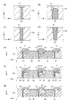
図1(a)は光電変換装置の一例として、裏面照射型の撮像装置の実施形態を示す断面図である。図1(b)は光電変換装置の一例として、表面照射型の撮像装置の実施形態を示す断面図である。まず、裏面照射型と裏面照射型に共通の事項を説明する。 FIG. 1A is a cross-sectional view showing an embodiment of a back-illuminated imaging device as an example of a photoelectric conversion device. FIG. 1B is a cross-sectional view showing an embodiment of a surface irradiation type imaging device as an example of a photoelectric conversion device. First, items common to the back-illuminated type and the back-illuminated type will be described.
光電変換装置1000は表面1と、表面1とは反対側の裏面2とを有する半導体層100を備える。半導体層100は例えば単結晶シリコン層であるが、光電変換が可能な半導体層であれば単結晶シリコン層に限らない。また、光電変換装置1000は、表面1の側に配され、半導体層100の溝11と溝11の中の絶縁体12によって構成された素子分離部10を備える。素子分離部10はSTI構造あるいはLOCOS構造を有し得る。素子分離部10を構成する絶縁体12は例えば酸化シリコンからなる。また、光電変換装置1000は、半導体層100に設けられた溝21によって構成された画素分離部20を備える。画素分離部20は、中間面3を通って配されている。中間面3は素子分離部10よりも裏面2の側に位置し、表面1および/または裏面2に沿った仮想的な平面である。中間面3は裏面2に平行でありうる。中間面3に垂直な方向を法線方向Nと称し、中間面3に平行な方向を面内方向Pと称する。法線方向Nにおいては、画素分離部20は中間面3に対して表面1側と裏面2側に両方に渡って延在している。中間面3の面内においては、画素分離部20を挟んで半導体層100が不連続になっている。画素分離部20の溝21の中には、固体22が存在していてもよいし、真空の空間あるいは気体が存在していてもよいし、気体と固体22の両方が配置されていてもよい。溝21の中に存在する固体22としては、絶縁体、導電体、半導体のいずれでもよい。溝21の中に存在する固体22としての絶縁体は酸化シリコンが典型的であるが、窒化シリコン、酸窒化シリコン、酸化タンタル、酸化ハフニウム、酸化チタンなどを用いることもできる。溝21の中に存在する固体22としての導電体は金属やポリシリコンが典型的であるが、アルミニウム、銅、タングステン、チタン、窒化チタン、タンタル、窒化タンタル、金属シリサイド等を用いることもできる。溝21の中に存在する固体22としての半導体は単結晶シリコンが典型的であるが、アモルファスシリコンであってもよい。溝21の中に存在する固体22としての半導体の導電型は、後述する光電変換素子で蓄積される信号電荷とは反対の導電型であることが好ましい。
The
半導体層100の表面1と裏面2との間には光電変換素子30が設けられている。光電変換素子30はフォトダイオードである。フォトダイオードとしての光電変換素子30は信号電荷(電子)を蓄積するための蓄積領域として機能するn型の不純物領域40と、不純物領域40とpn接合を成すp型の不純物領域50とを含む。p型の不純物領域50で光電変換により発生した電子は不純物領域40に蓄積される。中間面3内には不純物領域40が位置していることが好ましい。中間面3と裏面2との間には不純物領域50が位置している。ここでは電子蓄積型のフォトダイオードを例示したが、正孔蓄積型のフォトダイオードを採用することもできる。その場合には、不純物領域の導電型を電子蓄積型の場合の逆にすればよい。信号電荷が多数キャリアである導電型を第1導電型、信号電荷が少数キャリアである導電型を第2導電型とする。信号電荷が電子であれば、電子が多数キャリアであるn型が第1導電型である。なお、半導体層100内において光電変換素子30としてみなされる部分は、信号電荷として読み出される電荷を光電変換によって生じる部分である。厳密には、光電変換素子30としてみなされる部分は、半導体層100内の不純物濃度分布と印加される電圧に基づくポテンシャルプロファイルによって定まる。
A
半導体層100の表面1側には画素トランジスタ90が設けられている。図1では画素トランジスタ90のチャネル領域70とゲート電極80を記載している。画素トランジスタ90には、転送トランジスタや増幅トランジスタ、リセットトランジスタや選択トランジスタが含まれる。転送トランジスタは光電変換素子30の信号電荷を電荷検出領域に転送する。電荷検出領域は浮遊拡散領域(フローティングディフュージョン)で構成される。増幅トランジスタは電荷に基づく信号をソースフォロワ回路によって生成するもので、電荷検出領域に接続されたゲートを有する。リセットトランジスタは電荷検出領域に接続されたドレインを有し、光電変換素子30の電荷をリセットする。選択トランジスタは増幅トランジスタと出力線との接続/非接続を選択する。
A
半導体層100のうち、光電変換素子30の外側はp型の不純物領域60で構成される。このp型の不純物領域60は、同じくp型の不純物領域50に比べて不純物濃度が高くなっている。不純物領域60の一部は、画素間の電荷の混合を抑制するポテンシャル障壁として機能し得る。また、不純物領域60の一部は、半導体層100と絶縁体との界面で生じたノイズ電荷が光電変換素子30に取り込まれることを抑制するポテンシャル障壁として機能し得る。また、不純物領域60は接地電位などの固定電位を供給する導電部材が接続された、濃いp型のウェルコンタクトを含む。ウェルコンタクトから、不純物領域60を介して、光電変換素子30の不純物領域40に電位が供給される。
Of the
画素分離部20は光電変換素子30の周囲に配置される。画素分離部20は隣接する画素間での混色を抑制することが可能な構成を有する。光電変換素子30の周囲に配置された画素分離部20で囲まれた半導体領域上には、不純物領域40以外に、素子分離部10にて分離して配置される画素トランジスタが含まれるようにする。すなわち、中間面3内において隣接して向かい合う画素分離部20の間には光電変換素子30だけでなく、素子分離部10の下の半導体領域が含まれている。また、中間面3内において隣接して向かい合う画素分離部20の間には素子分離部10によって光電変換素子30から分離された画素トランジスタ90の下の半導体領域も含まれている。図1の例では、これら素子分離部10や画素トランジスタ90の下の半導体領域にまで光電変換素子30が配されている。
The
表面1側には複数の配線層310、320、330とそれらの周囲の複数の層間絶縁層からなる絶縁膜300が設けられている。なお、配線層で構成された出力線は光電変換素子30で生成された信号電荷を画素トランジスタ90を介して電気信号として後段に出力するように設けられている。
On the
図1(a)に示した裏面照射型の撮像装置では、裏面2側に誘電体膜410、遮光部材420、カラーフィルタアレイ430、マイクロレンズアレイ440が設けられている。誘電体膜410は保護膜(パッシベーション膜)、平坦化膜および/または反射防止膜として機能する。表面1側であって絶縁膜300の上には支持基板400が設けられている。支持基板400には信号処理回路等の集積回路を設けることもできる。半導体層100の厚さは1〜10μm程度である。支持基板の厚さは50〜800μm程度である。
In the back-illuminated image pickup apparatus shown in FIG. 1A, a
図1(b)に示した表面照射型の撮像装置では、表面1側であって絶縁膜200の上に、誘電体膜410、カラーフィルタアレイ430、マイクロレンズアレイ440が設けられている。誘電体膜410は保護膜(パッシベーション膜)、平坦化膜および/または反射防止膜として機能する。半導体層100の厚さは50〜800μm程度である。
In the surface-illuminated image pickup apparatus shown in FIG. 1B, a
カラーフィルタアレイ430は特定の波長の光のみを選択的に透過させるように設けられる。たとえば赤、緑、青の波長を透過するカラーフィルターを配列させても良い。また、白色光を透過させる画素を混在させても良い。なお各画素に対応して配置されたマイクロレンズアレイ440の各マイクロレンズは、入射光を光電変換素子30に集光させるように設けられている。
The
次に、図2を用いて、半導体層100およびその近傍の構造について詳細に説明する。
Next, the structure of the
半導体層100は、素子分離部10によって画定された素子領域を有する。素子領域は素子分離部10に対する位置によって区分される。素子領域の深さ方向の下端は素子分離部10の底面の深さに一致する。図2には半導体層100に含まれる素子領域として素子領域111、112、113、114を示している。素子領域111には光電変換素子41が設けられており、素子領域112には光電変換素子42が設けられている。素子領域113は、素子領域111と素子領域112との間に配されており、素子領域113にはトランジスタや容量素子、抵抗素子などの半導体素子が設けられている。素子領域113の形状は素子領域111や素子領域112の形状とは異なっている。素子領域113には光電変換素子30以外のトランジスタなどの半導体素子が設けられるからである。典型的には、素子領域113の面積は素子領域111や素子領域112の面積よりも小さくなっている。
The
本例では上述した素子領域113の半導体素子として画素トランジスタが設けられている。図2には画素トランジスタの不純物領域としてチャネル領域71を記載しているが、素子領域113にはソース領域やドレイン領域(不図示)も設けられている。チャネル領域71の上には画素トランジスタのゲート電極81が設けられている。素子領域114には光電変換素子43が設けられている。なお、図2において光電変換素子41、42、43として示した範囲は、図1において光電変換素子30の蓄積領域であるn型の不純物領域40に対応する。図2において光電変換素子41、42、43として示した範囲の外には光電変換素子41、42、43を成すp型の不純物領域50に対応する不純物領域が存在している。
In this example, a pixel transistor is provided as the semiconductor element in the
素子分離部10は、分離領域101、102、103を含む。分離領域101は素子領域111と素子領域113との間に位置する。分離領域102は素子領域112と素子領域113との間に位置する。分離領域103は素子領域111と素子領域114との間に位置する。
The
半導体層100は表面1側における素子領域と分離領域の分布に対応した半導体領域を素子分離部10よりも裏面2側に有する。裏面2側の半導体領域は、素子分離部10の分離領域あるいは素子領域に対する位置によって区分される。各半導体領域は、法線方向Nにおいて素子分離部10のいずれかの分離領域あるいは半導体層100のいずれかの素子領域と、裏面2との間に位置することになる。このような半導体領域として、半導体層100は、半導体領域121、122、123、124、125、126、127を含む。半導体領域121は素子領域111と裏面2との間に位置し、半導体領域122は素子領域112と裏面2との間に位置し、半導体領域123は素子領域113と裏面2との間に位置する。半導体領域127は素子領域114と裏面2との間に位置する。半導体領域124は分離領域101と裏面2との間に位置し、半導体領域125は分離領域102と裏面2との間に位置し、半導体領域126は分離領域103と裏面2との間に位置する。
The
画素分離部20は法線方向Nにおいて分離領域102に重なる第1部分201を有する。第1部分201は溝211により構成されている。面内方向Pにおいて、第1部分201は半導体領域122と半導体領域123との間に位置する。第1部分201によって半導体領域125は複数の部分に分割されている。その結果、半導体領域125は、第1部分201と半導体領域123との間に位置する部分1251と、第1部分201と半導体領域122との間に位置する部分1252と、を含んでいる。本例では、第1部分201が分離領域102に接続している。また、本例では、第1部分201が裏面2に達している。つまり、第1部分201を構成する溝21が裏面2に連続している。第1部分201と分離領域102とを離間させる場合には、第1部分201と分離領域102との間に半導体領域125の一部が位置することになる。第1部分201と裏面2とを離間させる場合には、第1部分201と裏面2との間に半導体領域125の一部が位置することになる。
The
画素分離部20は法線方向Nにおいて分離領域103に重なる第2部分202を有する。第2部分202は溝212により構成されている。面内方向Pにおいて、第2部分202は半導体領域121と半導体領域127との間に位置する。第2部分202によって半導体領域126は複数の部分に分割されている。その結果、第2部分202と半導体領域121との間に位置する部分1261と、第2部分202と半導体領域127との間に位置する部分1262と、を含んでいる。本例では、第2部分202が分離領域103に接続している。また、本例では、第2部分202が裏面2に達している。つまり、第2部分202を構成する溝212が裏面2に連続している。第2部分202と分離領域103とを離間させる場合には、第2部分202と分離領域103との間に半導体領域126の一部が位置することになる。第2部分202と裏面2とを離間させる場合には、第2部分202と裏面2との間に半導体領域126の一部が位置することになる。
The
このように、半導体領域122と半導体領域123は第1部分201によって不連続になっている。また、半導体領域121と半導体領域127は第2部分202によって不連続になっている。これにより、画素間の光の混合が低減され、光電変換装置の光学的特性が向上する。また、画素間の電荷の混合が低減され、光電変換装置の電気的特性が向上する。
As described above, the
一方、分離領域101と裏面2との間には画素分離部20が設けられていない。そのため、中間面3内において半導体領域121と半導体領域123が半導体領域124を介して連続している。つまり、中間面3において、素子領域111と素子領域113と分離領域101の下では半導体層100が連続している。このように、分離領域101の下で画素分離部20が設けられずに半導体層100が連続しているため、画素分離部20の溝21による光の散乱が抑制さる。このため、光電変換素子30に入射する光の量を増加させることができ、感度が向上する。また、ノイズ源となる画素分離部20を、光電変換素子30の蓄積領域としての不純物領域40から遠ざけることにより、画素分離部20の近傍で発生したノイズが光電変換素子30に取り込まれることを抑制できる。さらに、素子領域111や半導体領域121だけでなく、半導体領域124を光電変換素子30として利用することも可能となる。仮に半導体領域124に画素分離部20が配されていると、画素分離部20の分だけ光電変換素子30の体積が小さくなり、感度が低下する。
On the other hand, the
さらに、半導体領域124に隣接する半導体領域123をも光電変換素子として利用することが可能となる。仮に半導体領域124に画素分離部20が配されていると画素分離部20が半導体領域123と半導体領域121との間の電荷の移動を妨げてしまう。そのため、半導体領域123を光電変換素子として有効に利用することが困難になる。このように画素分離部20を設けないことで、光電変換素子を半導体領域121から半導体領域124、さらに半導体領域123まで延在させることで、感度を向上することができる。
Further, the
図1に示した例では、光電変換素子30を図2における半導体領域123、124に相当する領域まで配置している。これにより、光電変換素子30の中心とマイクロレンズの集光位置(典型的にはマイクロレンズの光軸)を一致させるあるいは近づけることが容易になる。マイクロレンズの集光位置とフォトダイオードの中心を近づけるには、マイクロレンズの光軸と分離領域101との距離を、マイクロレンズの光軸と分離領域103との距離よりも小さくすればよい。そうすれば、第1部分125と第2部分126から概ね等しい距離の位置にマイクロレンズで集光することができる。
In the example shown in FIG. 1, the
以上説明したように、画素分離部20を、半導体領域124から離して配置することで、光学的や電気的な面から光電変換性能を向上することができる。
As described above, by arranging the
図3(a)〜(d)は、素子分離部10と画素分離部20の形状および/または位置関係に関する変形例である。図3(a)に示すように、素子分離部10は裏面2側に向かって幅が狭くなるテーパー形状を有していてもよい。また、図3(a)に示すように、画素分離部20は表面1側に向かって幅が狭くなるテーパー形状を有していてもよい。なお素子分離部10の周囲にはチャネルストップとして機能する、光電変換素子30のp型の不純物領域50よりも濃いp型の不純物領域を配置することができる。画素分離部20の底部(表面1側)はチャネルストップ用の不純物領域に接するように設けるのが望ましい。これにより画素分離部20の底部と同様に暗電流を抑制することができる。
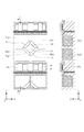
3 (a) to 3 (d) are modified examples relating to the shape and / or positional relationship between the
図3(b)に示す例では、画素分離部20は素子分離部10の離間した複数の分離領域に跨って配されている。複数の分離領域の間は素子領域である。このように、画素分離部20は素子領域に対向する部分を有していてもよい。
In the example shown in FIG. 3B, the
図3(c)に示すように、画素分離部20の一部は素子分離部10の最下面(裏面2側)よりも表面1側に位置していてもよい。図3(c)では、画素分離部20の側面が素子分離部10の側面よりも内側に位置していて、画素分離部20の表面1側の端部は素子分離部10に挟まれるようになっている。換言すると、画素分離部20が素子分離部10に食い込むように設けられているとも云える。このようにすることで画素分離部20の底部の周囲で発生するノイズを低減することが可能となる。素子分離部10の側面が画素分離部20に重なるように配置されていてもよい。
As shown in FIG. 3C, a part of the
図3(d)に示すように、画素分離部20は裏面2側に向かって幅が狭くなるテーパー形状を有していてもよい。また、画素分離部20は表面1側に露出していてもよい。また、図3(d)に示すように、素子分離部10の側面が画素分離部20の側面よりも内側に位置していて、素子分離部10が画素分離部20の表面1側の端部に挟まれるようになっていてもよい。
As shown in FIG. 3D, the
図3(e)〜(g)は不純物領域40、50、60の構成に関する変形例である。
3 (e) to 3 (g) are modified examples relating to the configuration of the
図3(e)の例では、不純物領域60は画素トランジスタ90のウェル61を含む。ウェル61を画素トランジスタの中心に対して非対称にしている。具体的には、ウェル61のうち、素子分離部10の分離領域101に重なる領域を、素子分離部10の分離領域102に重なる領域よりも小さくしている。これにより、分離領域101の下に配置する光電変換素子30の体積を増大して、感度を向上できる。
In the example of FIG. 3E, the
図3(f)の例では、ポテンシャル障壁として機能する濃いp型領域である不純物領域62、63の表面1に対する深さを異ならせている。不純物領域62は図2にて説明した、画素分離部20の周囲の半導体領域124に相当する半導体領域に配されている。不純物領域63は図2にて説明した、半導体領域125に相当する半導体領域に配されている。不純物領域63は不純物領域62よりも表面1に対して深くまで配されている。不純物領域63を深く配することで、画素分離部20と半導体層100との界面で発生するノイズが光電変換素子30に取り込まれ難くなっている。図2で説明した半導体領域125に配された不純物領域63を表面1に対して深く形成することで、画素分離部20からのノイズの発生を抑制することができる。
In the example of FIG. 3 (f), the depths of the
図3(g)の例では、光電変換素子30のn型の不純物領域40を図2で説明した半導体領域124、さらには半導体領域123にまで延在して設けている。このように、半導体領域124、123を有効に活用して不純物領域40の体積を大きくすることで、光電変換素子30の感度や飽和を向上することができる。
In the example of FIG. 3 (g), the n-
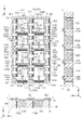
以下、図4〜7を用いて、画素のレイアウトの例を示す。なお、以下の例では上述した面内方向Pを互いに交差する(直交する)X方向とY方向に分けて記載する。また、法線方向Pについては、X方向およびY方向に交差する(直交する)Z方向として記載する。 Hereinafter, an example of pixel layout is shown with reference to FIGS. 4 to 7. In the following example, the above-mentioned in-plane direction P is described separately in the X direction and the Y direction that intersect (orthogonally) each other. Further, the normal direction P is described as the Z direction that intersects (orthogonally) the X direction and the Y direction.
図4を用いて、画素のレイアウトの第1例を示す。図4の例では、中間面3において、画素分離部20によって複数の半導体領域群に分離されている。画素分離部20で囲まれた半導体領域群の各々は、画素分離部20で分離されることなく連続した複数の半導体領域を含む。互いに分離された複数の半導体領域群は第1種類の半導体領域群Gsと第2種類の半導体領域群Gtに分類される。
FIG. 4 shows a first example of pixel layout. In the example of FIG. 4, the
第1種類の1つの半導体領域群Gsの上には3つの素子領域が配されている。 Three element regions are arranged on one semiconductor region group Gs of the first type.
半導体領域群Gsの上の3つの素子領域のうち、1つ目の素子領域には光電変換素子であるフォトダイオードPDmおよびフローティングディフュージョンFDmが配されている。 Of the three element regions above the semiconductor region group Gs, a photodiode PDm and a floating diffusion FDm, which are photoelectric conversion elements, are arranged in the first element region.
半導体領域群Gsの上の3つの素子領域のうち、2つ目の素子領域にはリセットトランジスタRSmが配されている。 A reset transistor RSm is arranged in the second element region of the three element regions above the semiconductor region group Gs.
半導体領域群Gsの上の3つの素子領域のうち、3つ目の素子領域にはウェルコンタクトWCmが配されている。ここで、mは半導体領域群毎に定められる1または3の数字であり、図4では半導体領域群ごとにPD1、PD3、RS1、RS3のように付して示している。なお、フォトダイオードPD3が配された素子領域が図2で説明した素子領域114に対応する。
Well contact WCm is arranged in the third element region among the three element regions above the semiconductor region group Gs. Here, m is a number of 1 or 3 determined for each semiconductor region group, and is shown in FIG. 4 as PD1, PD3, RS1, RS3 for each semiconductor region group. The element region in which the photodiode PD3 is arranged corresponds to the
第2種類の1つの半導体領域群Gtの上には3つの素子領域が配されている。半導体領域群Gtの上の3つの素子領域のうち、1つ目の素子領域には光電変換素子であるフォトダイオードPDnおよびフローティングディフュージョンFDnが配されている。半導体領域群Gtの上の3つの素子領域のうち、2つ目の素子領域には増幅トランジスタSFmおよび選択トランジスタSLmが配されている。半導体領域群Gsの上の3つの素子領域のうち、3つ目の素子領域にはウェルコンタクトWCnが配されている。ここで、nは半導体領域群毎に定められる2または4の数字であり、図4では、半導体領域群ごとにPD2、PD4、SF2、RS4のように付して示している。なお、フォトダイオードPD2が配された素子領域が図2で説明した素子領域112に対応し、フォトダイオードPD4が配された素子領域が図2で説明した素子領域111に対応する。また、増幅トランジスタSF2が配された素子領域が図2で説明した素子領域113に対応する。ウェルコンタクトWCn、WCmが配された素子領域の下の半導体領域も、図2で説明した素子領域113と同様に、フォトダイオードPD1が配された素子領域の下の半導体領域と連続している。
Three element regions are arranged on one semiconductor region group Gt of the second type. Of the three element regions above the semiconductor region group Gt, a photodiode PDn and a floating diffusion FDn, which are photoelectric conversion elements, are arranged in the first element region. Of the three element regions above the semiconductor region group Gt, the amplification transistor SFm and the selection transistor SLm are arranged in the second element region. Well contact WCn is arranged in the third element region among the three element regions above the semiconductor region group Gs. Here, n is a number of 2 or 4 determined for each semiconductor region group, and in FIG. 4, it is attached as PD2, PD4, SF2, RS4 for each semiconductor region group. The element region in which the photodiode PD2 is arranged corresponds to the
ウェルコンタクトWCm、WCnは光電変換素子30の不純物領域40に不純物領域60を介して電位を供給するための導電部材が接続されている。本例のように、半導体領域群Gs、Gt毎にウェルコンタクトWCn、WCmを配置することにより半導体領域群Gs、Gtに含まれる半導体領域やその上の素子領域の電位の制御性を高めることができ、安定した画像を得ることができる。
Well contacts WCm and WCn are connected to the
次に、図5を用いて、画素のレイアウトの第2例を示す。図5の例では、中間面3において、画素分離部20によって複数の半導体領域群に分離されている。画素分離部20で囲まれた半導体領域群の各々は、画素分離部20で分離されることなく連続した複数の半導体領域を含む。半導体領域群Grの上には4つの素子領域が配されている。
Next, a second example of the pixel layout is shown with reference to FIG. In the example of FIG. 5, the
半導体領域群Grの上の4つの素子領域のうち、1つ目の素子領域には光電変換素子であるフォトダイオードPDAp、PDBp、転送ゲートTXAp、TXBpおよびフローティングディフュージョンFDAp、FDBpが配されている。フォトダイオードPDApの信号電荷は転送ゲートTXApを介してフローティングディフュージョンFDApに転送される。フォトダイオードPDBpの信号電荷は転送ゲートTXBpを介してフローティングディフュージョンFDBpに転送される。フォトダイオードPDAp、PDBpにはそれぞれ共通のマイクロレンズが設けられる。つまり、1つのマイクロレンズに対してフォトダイオードPDAp、PDBpを別々に設けている。フォトダイオードPDAp、PDBpによって瞳分割された光線を別々に検出し、位相差検出方式による測距あるいは焦点検出が可能となる。また、フォトダイオードPDApとフォトダイオードPDBpの感度を異ならせて信号を合成することで、ダイナミックレンジの拡大を図ることもできる。本例ではフォトダイオードPDBpを画素トランジスタの下にまで延在させることで、フォトダイオードPDBpの感度をフォトダイオードPDApの感度よりも高めることもできる。 Of the four element regions above the semiconductor region group Gr, the photodiodes PDAp, PDBp, transfer gate TXAp, TXBp, and floating diffusion FDAp, FDBp, which are photoelectric conversion elements, are arranged in the first element region. The signal charge of the photodiode PDAp is transferred to the floating diffusion FDAp via the transfer gate TXAp. The signal charge of the photodiode PDBp is transferred to the floating diffusion FDBp via the transfer gate TXBp. A common microlens is provided for each of the photodiodes PDAp and PDBp. That is, the photodiodes PDAp and PDBp are separately provided for one microlens. The light rays divided into pupils by the photodiodes PDAp and PDBp are detected separately, and distance measurement or focus detection by a phase difference detection method becomes possible. Further, the dynamic range can be expanded by synthesizing signals with different sensitivities of the photodiode PDAp and the photodiode PDBp. In this example, by extending the photodiode PDBp below the pixel transistor, the sensitivity of the photodiode PDBp can be made higher than that of the photodiode PDAp.
半導体領域群Grの上の4つの素子領域のうち、2つ目の素子領域には光電変換素子であるフォトダイオードPDAq、PDBq、転送ゲートTXAq、TXBqおよびフローティングディフュージョンFDAq、FDBqが配されている。フォトダイオードPDAqの信号電荷は転送ゲートTXAqを介してフローティングディフュージョンFDAqに転送される。フォトダイオードPDBqの信号電荷は転送ゲートTXBqを介してフローティングディフュージョンFDBqに転送される。フォトダイオードPDAp、PDBpにはそれぞれ共通のマイクロレンズが設けられる。1つのマイクロレンズに対してフォトダイオードPDAq、PDBqを別々に設けている。フォトダイオードPDAp、PDBpによって瞳分割された光線を別々に検出し、位相差検出方式による測距あるいは焦点検出が可能となる。また、フォトダイオードPDAqとフォトダイオードPDBqの感度を異ならせて信号を合成することで、ダイナミックレンジの拡大を図ることもできる。本例ではフォトダイオードPDBqを画素トランジスタの下にまで延在させることで、フォトダイオードPDBqの感度をフォトダイオードPDAqの感度よりも高めることもできる。 Of the four element regions above the semiconductor region group Gr, the photodiodes PDAq, PDBq, transfer gate TXAq, TXBq, and floating diffusion FDAq, FDBq, which are photoelectric conversion elements, are arranged in the second element region. The signal charge of the photodiode PDAq is transferred to the floating diffusion FDAq via the transfer gate TXAq. The signal charge of the photodiode PDBq is transferred to the floating diffusion FDBq via the transfer gate TXBq. A common microlens is provided for each of the photodiodes PDAp and PDBp. Photodiodes PDAq and PDBq are separately provided for one microlens. The light rays divided into pupils by the photodiodes PDAp and PDBp are detected separately, and distance measurement or focus detection by a phase difference detection method becomes possible. Further, the dynamic range can be expanded by synthesizing signals with different sensitivities of the photodiode PDAq and the photodiode PDBq. In this example, by extending the photodiode PDBq below the pixel transistor, the sensitivity of the photodiode PDBq can be made higher than that of the photodiode PDAq.
ここで、pは半導体領域群Gr毎に定められる1、3、5および7から選ばれた数字である。図4では半導体領域Gr群ごとにPDA1、PDB3、FDA1、FDB3のように付して示している。なお、フォトダイオードPDA3、PDB3が配された素子領域が図2で説明した素子領域114に対応する。
Here, p is a number selected from 1, 3, 5 and 7 defined for each semiconductor region group Gr. In FIG. 4, PDA1, PDB3, FDA1, and FDB3 are attached to each semiconductor region Gr group. The element region in which the photodiodes PDA3 and PDB3 are arranged corresponds to the
ここで、qは半導体領域群Gr毎に定められる2、4、6および8から選ばれた数字である。図4では半導体領域群GrごとにPDA2、PDB4、FDA2、FDB4のように付して示している。なお、フォトダイオードPDA2、PDB2が配された素子領域が図2で説明した素子領域111に対応する。また、フォトダイオードPDA6、PDB6が配された素子領域が図2で説明した素子領域112に対応する。
Here, q is a number selected from 2, 4, 6 and 8 determined for each semiconductor region group Gr. In FIG. 4, PDA2, PDB4, FDA2, and FDB4 are attached to each semiconductor region group Gr. The element region in which the photodiodes PDA2 and PDB2 are arranged corresponds to the
半導体領域群Grの上の4つの素子領域のうち、3つ目の素子領域にはリセットトランジスタRSm、増幅トランジスタSFm、選択トランジスタSLmが配されている。半導体領域群Grの上の4つの素子領域のうち、4つ目の素子領域にはウェルコンタクトWCmが配されている。 A reset transistor RSm, an amplification transistor SFm, and a selection transistor SLm are arranged in the third element region among the four element regions above the semiconductor region group Gr. A well contact WCm is arranged in the fourth element region among the four element regions above the semiconductor region group Gr.
ここで、mは半導体領域群Gr毎に定められる1、2、3、4から選ばれた数字である。図4では半導体領域Gr群ごとにRS1、RS3、WC2、WC4のように付して示している。ここで、p=2×m−1およびq=2×mの関係になっている。なお、選択トランジスタSL1が配された素子領域が図2で説明した素子領域113に対応する。
Here, m is a number selected from 1, 2, 3, and 4 defined for each semiconductor region group Gr. In FIG. 4, RS1, RS3, WC2, and WC4 are attached to each semiconductor region Gr group. Here, the relationship is p = 2 × m-1 and q = 2 × m. The element region in which the selection transistor SL1 is arranged corresponds to the
本例でも第1例と同様に、半導体領域群Gr毎にウェルコンタクトWCn、WCmを配置することにより半導体領域群Grに含まれる半導体領域その上の素子領域の電位の制御性を高めることができ、安定した画像を得ることができる。 In this example as well, as in the first example, by arranging well contacts WCn and WCm for each semiconductor region group Gr, the controllability of the potential of the semiconductor region included in the semiconductor region group Gr and the element region above it can be enhanced. , A stable image can be obtained.
また、本例では、1つ目の素子領域に配されたフォトダイオードPDAp、PDBpと、2つ目の素子領域に配されたフォトダイオードPDAq、PDBqとが3つ目の素子領域に配されたトランジスタRSm、SFm、SLmを共有している。このようにトランジスタを共有するフォトダイードが配された素子領域の下の半導体領域を、画素分離部20で分離せずに1つの半導体領域群に含めている。このようにすることで、1つ目の素子領域に配されたフォトダイオードPDAp、PDBpと、2つ目の素子領域に配されたフォトダイオードPDAq、PDBqと、の信号の差を低減できる。
Further, in this example, the photodiodes PDAp and PDBp arranged in the first element region and the photodiodes PDAq and PDBq arranged in the second element region are arranged in the third element region. The transistors RSm, SFm, and SLm are shared. The semiconductor region below the element region in which the photodiode sharing the transistor is arranged is included in one semiconductor region group without being separated by the
また、隣接する複数のフォトダイオードを画素分離部20が囲むように配置されている。また、各画素を区画する領域の交差部には画素トランジスタが設けられている。そのような交差部に画素分離部20を設けていない。そして、リセットトランジスタRS、増幅トランジスタSF、選択トランジスタSL、あるいはウェルコンタクトWCを互いに共有するフォトダイオードを画素分離部20が囲んでいる。本例によれば、混色を抑制するとともに、画素分離部20によるトランジスタへの影響を低減することが可能となる。
Further, a plurality of adjacent photodiodes are arranged so as to be surrounded by the
次に、図6を用いて、画素のレイアウトの第3例を示す。図6の例では、中間面3のX方向において画素分離部20の第1部分201と第2部分202によって複数の半導体領域群に分離されている。X方向において画素分離部20に挟まれた半導体領域群の各々は、X方向において画素分離部20で分離されることなく連続した複数の半導体領域を含む。この点については第2例と同様である。なお、画素分離部20の同一の部分であっても、注目する光電変換素子に対する位置関係により図2で説明した第1部分201となるか第2部分202となるかは変わるので、図2では画素分離部20のある部分を部分201/202として示している。
Next, a third example of the pixel layout is shown with reference to FIG. In the example of FIG. 6, in the X direction of the
一方、本例では、X方向において画素分離部20で挟まれた半導体領域群の各々は、Y方向において画素分離部20の第3部分203で分離されている。このようにすることでY方向における画素間での分離性能を高めることができる。ただし、第3部分203は第1部分201や第2部分202からは不連続である。そのため、X方向において画素分離部20に挟まれた半導体領域群の各々は、Y方向において半導体領域群間で連続した半導体領域を含む。
On the other hand, in this example, each of the semiconductor region groups sandwiched by the
半導体領域群の1つ目の半導体領域の上の素子領域にはフォトダイオードPDAp、PDBpが配されている。別の半導体領域群の1つ目の半導体領域の上の素子領域にはフォトダイオードPDAq、PDBqが配されている。トランジスタRSm、SFm、SLmはフォトダイオードPDAp、PDBpとフォトダイオードPDAq、PDBqとで共有されている。 Photodiodes PDAp and PDBp are arranged in the element region above the first semiconductor region of the semiconductor region group. Photodiodes PDAq and PDBq are arranged in the element region above the first semiconductor region of another semiconductor region group. The transistors RSm, SFm, and SLm are shared by the photodiodes PDAp and PDBp and the photodiodes PDAq and PDBq.
そして、トランジスタRSm、SFm、SLmの下の半導体領域は画素分離部20で分離されずに、半導体領域群間で半導体領域が連続している。他にも半導体領域群の交差部など、画素分離部20で分離されずに、半導体領域群間で半導体領域が連続している部分を設けている。これは、画素分離部20のうち、隣接するフォトダイオードの間に配置された第3部分203が、第1部分201および第2部分202とは不連続になっているためである。
The semiconductor regions under the transistors RSm, SFm, and SLm are not separated by the
半導体領域群の間において、画素分離部20が設けられていない部分を設けることで、1つのウェルコタクトによる電位供給の範囲が広くなる。つまり、画素分離部20を不連続にすることにより隣接する画素のウェルを連通することでウェルの電位を揃えることができる。また、第1例や第2例に比べてウェルコンタクトの数を減らすことができる。その結果、ウェルコンタクトに起因するノイズの発生を抑制できる。
By providing a portion between the semiconductor region groups in which the
図7を用いて、画素のレイアウトの第4例を示す。図6の例では、素子分離部10はフォトダイオードのその周囲に設けられているトランジスタとの間に配されている。一方、隣接するフォトダイオード間には設けられていない。図示はしないが隣接するフォトダイオード間にはpn接合分離による拡散分離部が成されている。このために拡散分離部を挟んで配列されたフォトダイオードに沿って延在する素子分離部10に対応して画素分離部20が形成されている。
A fourth example of the pixel layout is shown with reference to FIG. In the example of FIG. 6, the
本例によれば、画素領域において列、あるいは行方向の混色を抑制するとともに、画素分離部20によるフォトダイオードへの影響を低減することが可能となる。
According to this example, it is possible to suppress color mixing in the column or row direction in the pixel region and reduce the influence of the
次に図8を用いて、本実施例に係る固体撮像装置の製造方法を説明する。 Next, a method of manufacturing the solid-state image sensor according to the present embodiment will be described with reference to FIG.
まず図8(a)に示す工程aでは、半導体基板SUBの表面F側に素子分離部10用の溝11が形成される。溝11の周囲にはイオン注入によりチャネルストップ層(不図示)が形成される。
First, in the step a shown in FIG. 8A, a
次に、図8(b)に示す工程bでは、溝11に素子分離部10のための絶縁体12を埋める。絶縁体12は酸化シリコンが好適である。溝11の外の余分な絶縁体はCMP法等により除去される。これにより、STI(Shallow Trench Isolation)構造を有する、素子分離部10が形成される。
Next, in the step b shown in FIG. 8B, the
次に、図8(c)に示す工程cでは、半導体基板SUBの表面F上にゲート絶縁膜(不図示)及びゲート電極80が積層されて画素トランジスタが形成(不図示)される。さらに、半導体基板SUBの表面F側から行われるイオン注入によって光電変換素子30や画素トランジスタのソース・ドレイン領域を形成する。
Next, in the step c shown in FIG. 8C, a gate insulating film (not shown) and a
次に、図8(d)に示す工程dでは、ゲート電極80を覆う絶縁層が積層された後に、絶縁層にコンタクトホールが形成される。さらにコンタクトホールが形成された絶縁層上に配線層および層間絶縁層を積層することで多層配線構造が形成される。本例では3層の配線層310、320、330を形成している。配線構造には、例えば銅配線やアルミニウム配線を用いることが可能である。
Next, in the step d shown in FIG. 8D, a contact hole is formed in the insulating layer after the insulating layer covering the
次に、図8(e)に示す工程eでは、絶縁膜300の上方から支持基板400が貼り合わされる。貼り合わせは接着剤による接合でも良いし、その他公知の方法を適宜用いることができる。ただし配線構造などに影響を与えないように400℃以下のプロセスで処理するのが好ましい。
Next, in the step e shown in FIG. 8E, the
次に、図8(f)に示す工程fでは、半導体基板SUBが所望の厚さになるまで、半導体基板SUBの裏面B1側から薄化処理が施される。この半導体基板SUBの薄化は裏面B1に代わって新たな裏面B2が現れる。裏面B2には光電変換素子30が臨むように行われてもよい。例えば、化学機械研磨法(CMP)や、ドライエッチング、ウェットエッチングなどを用いることができる。またこれら手法を組合せることも可能である。例えば薄化された半導体基板SUBの膜厚は1〜10μmの範囲とし、またフォトダイオードの受光感度の向上、あるいは半導体基板の機械的な強度の観点から、2〜5μmの範囲とすることが好ましい。
Next, in the step f shown in FIG. 8 (f), thinning treatment is performed from the back surface B1 side of the semiconductor substrate SUB until the semiconductor substrate SUB has a desired thickness. This thinning of the semiconductor substrate SUB causes a new back surface B2 to appear in place of the back surface B1. The
次に図8(g)に示す工程gでは、半導体基板の表面F側に形成された素子分離部10に対向する位置において、半導体基板の裏面B2側から画素分離部20の溝21が形成される。このとき画素分離部20の溝21の裏面B2に対する深さは、画素分離部20の底部が素子分離部10に達する深さとするのがよい。例えば薄化処理された半導体基板SUBの厚さが約2μmの場合に素子分離部10の深さが約0.3μmとすると、対向して配置される溝21の深さが約1.7μmとなるように形成される。このような画素分離部20は以下の手順で形成される。なお画素分離部20の底部の幅は、素子分離部10の底部の幅に対して相対的に狭くすると良い。これによりアライメントズレが生じた場合においても、画素分離部20の底部を素子分離部10の底部に接することが容易になる。
Next, in the step g shown in FIG. 8 (g), a
画素分離部20の溝21は光電変換素子30に隣接する素子分離部10の一部の分離領域101の下には設けない。これにより、上述した光電変換性能の向上が可能となる。
The
画素分離部20の形成方法について、より詳細に説明する。まず画素分離部20の溝21を半導体基板SUBに形成するため、例えば異方性のドライエッチング法を用いることで、所望の幅を有する溝21を形成する。なお画素分離部20の溝21をドライエッチングにより加工する際には、半導体基板SUBのエッチングの終端検出として素子分離部10を利用しても良い。あるいは半導体基板SUBの膜厚に応じてエッチング時間を指定してエッチングしても良い。また素子分離膜10の底部の一部をエッチングするようにしても良い。
The method of forming the
次に、次に図8(g)に示す工程gでは、溝21の中に固体22を形成する。まず、半導体層100の裏面2で発生する暗電流を抑制するための固定電荷膜(不図示)を形成する。このために半導体基板SUBの裏面B2の形状に沿って固定電荷膜(不図示)が形成される。この固定電荷膜は、少なくとも半導体基板SUBの裏面B2上に形成され、さらに画素分離部20の溝21の側壁や底面を被覆するように形成しても良い。このように画素分離部20の側壁や底面を固定電荷膜で被覆することで、例えば溝21の表面で発生しうる暗電流も抑制することが可能となる。なお固定電荷膜としては、たとえば原子層堆積法(ALD)により酸化ハフニウム膜を用いることができる。
Next, in the step g shown in FIG. 8 (g), the solid 22 is formed in the
次に、半導体基板SUBの画素分離部20の内部に誘電体、金属材料、その他の遮光性を備えた材料、あるいはそれらを組み合わせた材料からなる固体22を形成する。例えば、酸化シリコン膜や酸化チタン膜などの半導体基板SUBを成すシリコンよりも低い屈折率を有する材料を固定電荷膜上に形成する。続いて化学気相成長法(CVD)や原子層堆積法(ALD)を用いて導電材料を埋設させて画素分離部20を形成することができる。あるいは原子層堆積法(ALD)を用いて酸化シリコン膜を固定電荷膜上に形成した後に、HDP(High Density Plasma)CVD法を用いて酸化シリコン膜を堆積する。このように2層構造の絶縁膜で埋設させて画素分離部20を形成しても良い。特に400℃以下の低温で形成できる材料が好ましく、例えばP型不純物をドープしたアモルファスシリコン、銅、タングステンなどを化学気相成長法(CVD)や原子層堆積法(ALD)などで形成するのが望ましい。なお、上述した固定電荷膜を固体22として用いてもよい。
Next, a solid 22 made of a dielectric, a metal material, another material having a light-shielding property, or a material obtained by combining them is formed inside the
なお上記で画素分離部20の内部に固体22を埋設する事例について説明しているが、溝21内の構成はこれらに限定されるものではなく、混色を抑制可能な構造であれば良く、公知の構成及び製法を適用することが可能である。また例えば画素分離部20は溝21の一部または全部が空洞であっても構わない。
Although the case where the solid 22 is embedded inside the
なお本例では、画素分離部20を半導体基板の裏面B2側から形成する場合について説明したが、画素分離部20の形成方法はここで説明する方法に限定されるものではない。例えば、工程a、bで説明した素子分離部10を形成する前に、半導体基板SUBの表面F側から溝21を形成しても良い。
In this example, the case where the
この後は図1(a)に示す構造を形成する。半導体基板SUBの裏面B2側に誘電体膜410が形成され、誘電体膜410上の画素間に遮光部材420がパターニングされる。遮光部材420はスパッタ法や化学気相成長法(CVD)により成膜された後、画素間を含む遮光構造を必要とする部分以外を除去するように加工が行われることにより形成される。遮光部材420の材料としては、例えば、チタンとタングステンの積層膜、あるいは窒化チタンとタングステンの積層膜などを用いることができる。
After that, the structure shown in FIG. 1A is formed. A
次に平坦化膜(不図示)を形成し、平坦化膜上に各画素に対応して例えば赤、緑、青のカラーフィルタアレイ410を形成し、その上にマイクロレンズアレイ440を形成する。各カラーフィルター及びマイクロレンズは、画素アレイの各単位画素に対応して形成される。以上により、光電変換装置を完成させる。半導体基板SUBは上述した半導体層100として用いられる。
Next, a flattening film (not shown) is formed, a red, green, and blue
上述した例によれば、また画素分離部20を素子分離部10にまで深さ方向に伸ばすことで、隣接する画素間での混色を効果的に抑制することが可能である。画素分離部20を光電変換素子だけでなく、トランジスタ等が設けられた素子領域の下の半導体領域をも囲むように配置することができる。これにより、光電変換素子によって光電変換を行う範囲を広くすることが可能となる。
According to the above-mentioned example, by extending the
以上説明した光電変換装置はカメラの撮像装置(イメージセンサ)に適用できる。カメラは撮像装置以外に、撮像装置から得られた信号を処理する信号処理装置、撮像装置から得られた信号を記憶する記憶装置、および、撮像装置で得られた情報を表示する表示装置の少なくとも1つを備えることができる。ここでいうカメラとはスチルカメラやビデオカメラ、監視カメラ等のカメラ専用機器以外に、撮影機能を有する情報端末や撮影機能を有する移動体(車両や飛行体)も包含する。 The photoelectric conversion device described above can be applied to an image pickup device (image sensor) of a camera. In addition to the image pickup device, the camera is at least a signal processing device that processes a signal obtained from the image pickup device, a storage device that stores a signal obtained from the image pickup device, and a display device that displays information obtained by the image pickup device. One can be provided. The term "camera" as used herein includes not only camera-dedicated devices such as still cameras, video cameras, and surveillance cameras, but also information terminals having a shooting function and moving objects (vehicles and flying bodies) having a shooting function.
また、本明細書に明確な記載がなくとも、添付の図面や技術常識から把握できる事項も本開示の一部を構成する。本発明は、本開示の技術思想の範囲を逸脱しない限り、適宜な変更が可能である。 In addition, even if there is no clear description in this specification, matters that can be grasped from the attached drawings and common general technical knowledge also form a part of this disclosure. The present invention can be appropriately modified as long as it does not deviate from the scope of the technical idea of the present disclosure.
1 表面
2 裏面
3 中間面
100 半導体層
10 素子分離部
12 絶縁体
20 画素分離部
21 溝
111、112、113 素子領域
101、102、103 分離領域
121、122、123、124 半導体領域
1
Claims (12)
前記半導体層は、
少なくとも4つの光電変換素子が配された第1領域と、
前記第2面に沿って設けられ、且つ前記第1面よりも前記第2面の近くに位置する仮想面をとったときに、
前記半導体層内に設けられ、且つ仮想面を通る溝によって構成された第1分離部と、
前記半導体層内に設けられ、且つ前記仮想面を通る溝によって構成された第2分離部と、
前記半導体層内に設けられ、第1絶縁体を含み、前記第1面側に配された第3分離部と、
前記第1面の上に配されたゲート電極を有し、前記少なくとも4つの光電変換素子からの信号を読み出すための第1トランジスタと、を有し、
前記第1面における平面視において、前記第1分離部と、前記第1領域と、前記第3分離部と、前記第1トランジスタと、前記第2分離部とがこの順に設けられ、
前記仮想面の前記第1分離部の前記溝と前記第2分離部の溝との間の部分において、前記第1分離部と、前記第1領域と、前記第3分離部と、前記第1トランジスタと、前記第2分離部がこの順に配された方向に沿って、前記半導体層は連続した半導体領域を有することを特徴とする光電変換装置。 A photoelectric conversion device having a semiconductor layer having a first surface and a second surface opposite to the first surface.
The semiconductor layer is
In the first region where at least four photoelectric conversion elements are arranged,
When a virtual surface provided along the second surface and located closer to the second surface than the first surface is taken.
A first separation portion provided in the semiconductor layer and formed by a groove passing through a virtual surface,
A second separation portion provided in the semiconductor layer and formed by a groove passing through the virtual surface,
A third separation portion provided in the semiconductor layer, including a first insulator, and arranged on the first surface side.
It has a gate electrode arranged on the first surface, and has a first transistor for reading signals from the at least four photoelectric conversion elements.
In a plan view on the first surface, the first separation portion, the first region, the third separation portion, the first transistor, and the second separation portion are provided in this order.
In the portion of the virtual surface between the groove of the first separation portion and the groove of the second separation portion, the first separation portion, the first region, the third separation portion, and the first A photoelectric conversion device characterized in that the semiconductor layer has a continuous semiconductor region along a direction in which a transistor and a second separation portion are arranged in this order .
前記第1素子領域と前記第2素子領域は、前記第3分離部によって画定されていることを特徴とする請求項1に記載の光電変換装置。 The at least four photoelectric conversion elements are arranged in the first element region, and the first transistor is arranged in the second element region.
The photoelectric conversion device according to claim 1 , wherein the first element region and the second element region are defined by the third separation unit.
前記第1分離部と、前記第1領域と、前記第3分離部と、前記第1トランジスタと、前記第2分離部と、前記別の光電変換素子とがこの順に配され、
前記第1面に対する平面視において、前記第2分離部は前記第4分離部に重畳することを特徴とする請求項1または2に記載の光電変換装置。 The semiconductor layer has yet another photoelectric conversion element and a fourth separation portion including a second insulator and arranged on the first surface side.
The first separation unit, the first region, the third separation unit, the first transistor, the second separation unit, and the other photoelectric conversion element are arranged in this order.
The photoelectric conversion device according to claim 1 or 2 , wherein the second separation portion is superimposed on the fourth separation portion in a plan view with respect to the first surface.
前記第2トランジスタと、前記第1分離部と、前記第1領域と、前記第3分離部と、前記第1トランジスタと、前記第2分離部と、前記別の光電変換素子とがこの順に配され、前記第1面に対する平面視において、前記第2分離部は前記第4分離部に重畳し、前記第1分離部は前記第5分離部に重畳することを特徴とする請求項3に記載の光電変換装置。 The semiconductor layer further includes a second transistor and a fifth separation portion including an insulator and arranged on the first surface side.
The second transistor, the first separation unit, the first region, the third separation unit, the first transistor, the second separation unit, and the other photoelectric conversion element are arranged in this order. It is, in a plan view with respect to the first surface, according to claim 3, wherein the second separation unit is superimposed on the fourth separation unit, wherein the first separation unit is characterized in that superimposed on the fifth separation unit Photoelectric conversion device.
前記半導体層は、信号電荷が少数キャリアである第2導電型の第2不純物領域を有し、前記第2不純物領域は、2つの前記第1導電型の半導体領域の間に設けられていることを特徴とする請求項1乃至4のいずれか1項に記載の光電変換装置。 Each of the at least four photoelectric conversion elements has a first conductive type impurity region in which the signal charge is a large number of carriers.
The semiconductor layer has a second conductive type second impurity region in which the signal charge is a minority carrier, and the second impurity region is provided between the two first conductive type semiconductor regions. The photoelectric conversion device according to any one of claims 1 to 4 , wherein the photoelectric conversion device is characterized.
前記第1面に対する平面視において、前記第1光電変換素子と前記第4光電変換素子は第1方向に沿って配され、前記第2光電変換素子と前記第3光電変換素子は、前記第1方向と交わる第2方向に沿って配されていることを特徴とする請求項1乃至5のいずれか1項に記載の光電変換装置。 The at least four photoelectric conversion elements include a first photoelectric conversion element, a second photoelectric conversion element, a third photoelectric conversion element, and a fourth photoelectric conversion element.
In a plan view with respect to the first surface, the first photoelectric conversion element and the fourth photoelectric conversion element are arranged along the first direction, and the second photoelectric conversion element and the third photoelectric conversion element are the first. The photoelectric conversion device according to any one of claims 1 to 5 , wherein the photoelectric conversion device is arranged along a second direction intersecting the directions.
前記第1面に対する平面視において、前記フローティングディフュージョン領域は、前記第1光電変換素子と前記第4光電変換素子との間に位置し、前記第2光電変換素子と前記第3光電変換素子との間に位置することを特徴津する請求項6に記載の光電変換装置。 The semiconductor layer includes a floating diffusion region in which charges generated by at least four photoelectric conversion elements are transferred, and a first transfer transistor that controls conduction between the first photoelectric conversion element and the floating diffusion region. A second transfer transistor that controls the conduction between the second photoelectric conversion element and the floating diffusion region, and a third transfer transistor that controls the continuity between the third photoelectric conversion element and the floating diffusion region. A fourth transfer transistor that controls continuity between the fourth photoelectric conversion element and the floating diffusion region.
In a plan view with respect to the first surface, the floating diffusion region is located between the first photoelectric conversion element and the fourth photoelectric conversion element, and the second photoelectric conversion element and the third photoelectric conversion element are associated with each other. The photoelectric conversion device according to claim 6 , characterized in that it is located between them.
前記第1面に対する平面視において、前記第1トランジスタのソースとドレインを結ぶ第1仮想線は、前記第2光電変換素子と前記第4光電変換素子とを結ぶ第2仮想線と平行になることを特徴とする請求項7に記載の光電変換装置。 The semiconductor layer has a gate electrode arranged on the first surface, and has a first transistor for reading signals from the at least four photoelectric conversion elements.
In a plan view of the first surface, the first virtual line connecting the source and drain of the first transistor is parallel to the second virtual line connecting the second photoelectric conversion element and the fourth photoelectric conversion element. 7. The photoelectric conversion device according to claim 7 .
前記光電変換装置から得られた信号を処理する信号処理装置、前記光電変換装置から得られた信号を記憶する記憶装置、および、前記光電変換装置で得られた情報を表示する表示装置の少なくともいずれかを備えるカメラ。 The photoelectric conversion device according to any one of claims 1 to 11 .
At least one of a signal processing device that processes a signal obtained from the photoelectric conversion device, a storage device that stores a signal obtained from the photoelectric conversion device, and a display device that displays information obtained by the photoelectric conversion device. A camera equipped with a signal.
Priority Applications (7)
| Application Number | Priority Date | Filing Date | Title |
|---|---|---|---|
| JP2016072989A JP6789653B2 (en) | 2016-03-31 | 2016-03-31 | Photoelectric converter and camera |
| US15/468,865 US10553634B2 (en) | 2016-03-31 | 2017-03-24 | Photoelectric conversion apparatus and camera |
| CN202210517086.XA CN114914260A (en) | 2016-03-31 | 2017-03-29 | Photoelectric conversion device and camera |
| CN201710197850.9A CN107275352B (en) | 2016-03-31 | 2017-03-29 | Photoelectric conversion device and camera |
| US16/717,252 US11430822B2 (en) | 2016-03-31 | 2019-12-17 | Photoelectric conversion apparatus and camera |
| US17/813,510 US11791360B2 (en) | 2016-03-31 | 2022-07-19 | Photoelectric conversion apparatus and camera |
| US18/465,072 US20230420474A1 (en) | 2016-03-31 | 2023-09-11 | Photoelectric conversion apparatus and camera |
Applications Claiming Priority (1)
| Application Number | Priority Date | Filing Date | Title |
|---|---|---|---|
| JP2016072989A JP6789653B2 (en) | 2016-03-31 | 2016-03-31 | Photoelectric converter and camera |
Related Child Applications (1)
| Application Number | Title | Priority Date | Filing Date |
|---|---|---|---|
| JP2020184153A Division JP7059336B2 (en) | 2020-11-04 | 2020-11-04 | Photoelectric converters and cameras |
Publications (3)
| Publication Number | Publication Date |
|---|---|
| JP2017183661A JP2017183661A (en) | 2017-10-05 |
| JP2017183661A5 JP2017183661A5 (en) | 2019-12-26 |
| JP6789653B2 true JP6789653B2 (en) | 2020-11-25 |
Family
ID=59961975
Family Applications (1)
| Application Number | Title | Priority Date | Filing Date |
|---|---|---|---|
| JP2016072989A Active JP6789653B2 (en) | 2016-03-31 | 2016-03-31 | Photoelectric converter and camera |
Country Status (3)
| Country | Link |
|---|---|
| US (4) | US10553634B2 (en) |
| JP (1) | JP6789653B2 (en) |
| CN (2) | CN107275352B (en) |
Families Citing this family (12)
| Publication number | Priority date | Publication date | Assignee | Title |
|---|---|---|---|---|
| JP6789653B2 (en) * | 2016-03-31 | 2020-11-25 | キヤノン株式会社 | Photoelectric converter and camera |
| KR102498582B1 (en) * | 2018-02-26 | 2023-02-14 | 에스케이하이닉스 주식회사 | Image Sensor Including Partition Patterns |
| JP2019165066A (en) * | 2018-03-19 | 2019-09-26 | ソニーセミコンダクタソリューションズ株式会社 | Imaging element and electronic device |
| US10893222B2 (en) * | 2018-03-29 | 2021-01-12 | Panasonic Intellectual Property Management Co., Ltd. | Imaging device and camera system, and driving method of imaging device |
| JP2019212900A (en) * | 2018-05-31 | 2019-12-12 | パナソニックIpマネジメント株式会社 | Imaging apparatus |
| KR20200040131A (en) | 2018-10-08 | 2020-04-17 | 삼성전자주식회사 | Image sensor and method of fabricating the same |
| TW202032773A (en) * | 2019-02-01 | 2020-09-01 | 日商索尼半導體解決方案公司 | Light-receiving element, solid-state imaging device, and ranging device |
| JP2020162100A (en) * | 2019-03-28 | 2020-10-01 | ソニーセミコンダクタソリューションズ株式会社 | Light receiving device and range finding module |
| JP2020161779A (en) * | 2019-03-28 | 2020-10-01 | ソニーセミコンダクタソリューションズ株式会社 | Light receiving device and range finding module |
| KR102358599B1 (en) * | 2019-09-30 | 2022-02-08 | 선전 구딕스 테크놀로지 컴퍼니, 리미티드 | Semiconductor structures, chips and electronic devices of image sensors |
| JP7433863B2 (en) * | 2019-11-27 | 2024-02-20 | キヤノン株式会社 | Photoelectric conversion devices, imaging systems, and mobile objects |
| JP2022112240A (en) * | 2021-01-21 | 2022-08-02 | ソニーセミコンダクタソリューションズ株式会社 | Light detection device and electronic apparatus |
Family Cites Families (71)
| Publication number | Priority date | Publication date | Assignee | Title |
|---|---|---|---|---|
| JPS61263266A (en) | 1985-05-17 | 1986-11-21 | Olympus Optical Co Ltd | Solid state image sensor |
| US6388305B1 (en) * | 1999-12-17 | 2002-05-14 | International Business Machines Corporation | Electrically programmable antifuses and methods for forming the same |
| KR20040031119A (en) * | 2002-10-04 | 2004-04-13 | (주)그래픽테크노재팬 | Image Sensor Having Isolator |
| JP4539176B2 (en) * | 2004-05-31 | 2010-09-08 | ソニー株式会社 | Solid-state imaging device and manufacturing method thereof |
| US7605415B2 (en) * | 2004-06-07 | 2009-10-20 | Canon Kabushiki Kaisha | Image pickup device comprising photoelectric conversation unit, floating diffusion region and guard ring |
| JP4742523B2 (en) | 2004-06-14 | 2011-08-10 | ソニー株式会社 | Solid-state imaging device and driving method thereof |
| JP4756839B2 (en) * | 2004-09-01 | 2011-08-24 | キヤノン株式会社 | Solid-state imaging device and camera |
| US8049293B2 (en) * | 2005-03-07 | 2011-11-01 | Sony Corporation | Solid-state image pickup device, electronic apparatus using such solid-state image pickup device and method of manufacturing solid-state image pickup device |
| JP4578329B2 (en) * | 2005-06-03 | 2010-11-10 | ルネサスエレクトロニクス株式会社 | Semiconductor memory device |
| JP2007095917A (en) * | 2005-09-28 | 2007-04-12 | Matsushita Electric Ind Co Ltd | Solid-state imaging device |
| US7586139B2 (en) | 2006-02-17 | 2009-09-08 | International Business Machines Corporation | Photo-sensor and pixel array with backside illumination and method of forming the photo-sensor |
| JP5328207B2 (en) * | 2008-04-01 | 2013-10-30 | キヤノン株式会社 | Solid-state imaging device |
| JP5314914B2 (en) | 2008-04-04 | 2013-10-16 | キヤノン株式会社 | Photoelectric conversion device, imaging system, design method, and photoelectric conversion device manufacturing method |
| EP2109143B1 (en) | 2008-04-09 | 2013-05-29 | Sony Corporation | Solid-state imaging device, production method thereof, and electronic device |
| JP2009272596A (en) | 2008-04-09 | 2009-11-19 | Sony Corp | Solid-state imaging device, method of manufacturing the same, and electronic instrument |
| JP4759590B2 (en) * | 2008-05-09 | 2011-08-31 | キヤノン株式会社 | Photoelectric conversion device and imaging system using the same |
| JP5353201B2 (en) | 2008-11-21 | 2013-11-27 | ソニー株式会社 | Method for manufacturing solid-state imaging device |
| JP5558857B2 (en) * | 2009-03-09 | 2014-07-23 | キヤノン株式会社 | Photoelectric conversion device and imaging system using the same |
| JP5470928B2 (en) | 2009-03-11 | 2014-04-16 | ソニー株式会社 | Method for manufacturing solid-state imaging device |
| JP2010225818A (en) * | 2009-03-23 | 2010-10-07 | Toshiba Corp | Solid-state image pickup device and method for manufacturing the same |
| JP5539105B2 (en) | 2009-09-24 | 2014-07-02 | キヤノン株式会社 | Photoelectric conversion device and imaging system using the same |
| JP5564874B2 (en) * | 2009-09-25 | 2014-08-06 | ソニー株式会社 | Solid-state imaging device and electronic apparatus |
| JP5564909B2 (en) | 2009-11-30 | 2014-08-06 | ソニー株式会社 | SOLID-STATE IMAGING DEVICE, ITS MANUFACTURING METHOD, AND ELECTRONIC DEVICE |
| JP5679653B2 (en) * | 2009-12-09 | 2015-03-04 | キヤノン株式会社 | Photoelectric conversion device and imaging system using the same |
| CN102668081B (en) * | 2009-12-26 | 2016-02-03 | 佳能株式会社 | Solid-state image pickup apparatus and image picking system |
| FR2955701A1 (en) * | 2010-01-28 | 2011-07-29 | St Microelectronics Sa | COMPACT IMAGE SENSOR STRUCTURE |
| JP2011159757A (en) * | 2010-01-29 | 2011-08-18 | Sony Corp | Solid-state imaging device and manufacturing method thereof, driving method of solid-state imaging device, and electronic device |
| KR101738532B1 (en) * | 2010-05-25 | 2017-05-22 | 삼성전자 주식회사 | A Backside Illumination Image Sensor Including an Upper High-doped Region and a Method of Fabricating the Same |
| JP2012015274A (en) * | 2010-06-30 | 2012-01-19 | Canon Inc | Solid-state imaging apparatus, and method of manufacturing the same |
| US8378398B2 (en) * | 2010-09-30 | 2013-02-19 | Omnivision Technologies, Inc. | Photodetector isolation in image sensors |
| US8101450B1 (en) * | 2010-12-13 | 2012-01-24 | Omnivision Technologies, Inc. | Photodetector isolation in image sensors |
| JP2012164768A (en) * | 2011-02-04 | 2012-08-30 | Toshiba Corp | Solid state image pickup device |
| JP6299058B2 (en) * | 2011-03-02 | 2018-03-28 | ソニー株式会社 | Solid-state imaging device, method for manufacturing solid-state imaging device, and electronic apparatus |
| JP5999402B2 (en) * | 2011-08-12 | 2016-09-28 | ソニー株式会社 | Solid-state imaging device, manufacturing method, and electronic apparatus |
| JP6003291B2 (en) * | 2011-08-22 | 2016-10-05 | ソニー株式会社 | Solid-state imaging device and electronic apparatus |
| JP5743837B2 (en) * | 2011-10-07 | 2015-07-01 | キヤノン株式会社 | Photoelectric conversion device, imaging device, and imaging system |
| US8686342B2 (en) * | 2012-04-09 | 2014-04-01 | Omnivision Technologies, Inc. | Double-sided image sensor formed on a single semiconductor wafer die |
| KR20140006370A (en) * | 2012-07-04 | 2014-01-16 | 삼성전자주식회사 | Semiconductor devices |
| JP2014022561A (en) * | 2012-07-18 | 2014-02-03 | Sony Corp | Solid-state imaging device and electronic apparatus |
| US9142580B2 (en) * | 2012-08-10 | 2015-09-22 | Canon Kabushiki Kaisha | Image pickup apparatus and image pickup system |
| US9659991B2 (en) * | 2012-10-22 | 2017-05-23 | Canon Kabushiki Kaisha | Image capturing apparatus, manufacturing method thereof, and camera |
| JP2014086514A (en) * | 2012-10-22 | 2014-05-12 | Canon Inc | Solid state imaging device, method for manufacturing the same, and camera |
| US9165959B2 (en) * | 2013-02-25 | 2015-10-20 | Omnivision Technologies, Inc. | Image sensor with pixel units having mirrored transistor layout |
| JP6278608B2 (en) * | 2013-04-08 | 2018-02-14 | キヤノン株式会社 | Semiconductor device and manufacturing method thereof |
| JP2014225536A (en) * | 2013-05-15 | 2014-12-04 | キヤノン株式会社 | Solid-state imaging device and camera |
| US20150054997A1 (en) * | 2013-08-23 | 2015-02-26 | Aptina Imaging Corporation | Image sensors having pixel arrays with non-uniform pixel sizes |
| JP6305030B2 (en) | 2013-11-22 | 2018-04-04 | キヤノン株式会社 | Method for manufacturing photoelectric conversion device |
| JP6305028B2 (en) * | 2013-11-22 | 2018-04-04 | キヤノン株式会社 | Method for manufacturing photoelectric conversion device and photoelectric conversion device |
| JP6282109B2 (en) * | 2013-12-26 | 2018-02-21 | キヤノン株式会社 | Imaging device manufacturing method and imaging device |
| JP6152060B2 (en) | 2014-02-14 | 2017-06-21 | キヤノン株式会社 | Solid-state imaging device and camera |
| KR102209097B1 (en) | 2014-02-27 | 2021-01-28 | 삼성전자주식회사 | Image sensor and method of fabricating the same |
| CN103824869B (en) * | 2014-03-17 | 2017-02-15 | 北京思比科微电子技术股份有限公司 | Image sensor pixel structure for preventing image diffusion and manufacturing method thereof |
| KR102212138B1 (en) * | 2014-08-19 | 2021-02-04 | 삼성전자주식회사 | Unit pixel for image sensor and pixel array comprising the same |
| US9711558B2 (en) * | 2014-09-12 | 2017-07-18 | Panasonic Intellectual Property Management Co., Ltd. | Imaging device with photoelectric converter |
| JP2016187018A (en) * | 2015-03-27 | 2016-10-27 | キヤノン株式会社 | Photoelectric conversion device and camera |
| US9768213B2 (en) * | 2015-06-03 | 2017-09-19 | Canon Kabushiki Kaisha | Solid-state image sensor and camera |
| US9653511B2 (en) * | 2015-08-11 | 2017-05-16 | Omnivision Technologies, Inc. | CMOS image sensor with peninsular ground contracts and method of manufacturing the same |
| KR102481481B1 (en) * | 2015-12-15 | 2022-12-26 | 삼성전자 주식회사 | Image sensor and method of manufacturing the same |
| JP6789653B2 (en) * | 2016-03-31 | 2020-11-25 | キヤノン株式会社 | Photoelectric converter and camera |
| JP6808348B2 (en) * | 2016-04-28 | 2021-01-06 | キヤノン株式会社 | Photoelectric converter and camera |
| JP7013119B2 (en) * | 2016-07-21 | 2022-01-31 | キヤノン株式会社 | Solid-state image sensor, manufacturing method of solid-state image sensor, and image pickup system |
| KR102589016B1 (en) * | 2016-08-25 | 2023-10-16 | 삼성전자주식회사 | Semiconductor devices |
| KR20180076054A (en) * | 2016-12-27 | 2018-07-05 | 삼성전자주식회사 | Image sensor comprising shared pixel, and electronic apparatus comprising the image sensor |
| KR20180076845A (en) * | 2016-12-28 | 2018-07-06 | 삼성전자주식회사 | Image sensor |
| US10079261B1 (en) * | 2017-08-17 | 2018-09-18 | Omnivision Technologies, Inc. | Raised electrode to reduce dark current |
| US10566380B2 (en) * | 2017-10-18 | 2020-02-18 | Omnivision Technologies, Inc. | Image sensor with dual trench isolation structures at different isolation structure depths |
| KR102542614B1 (en) * | 2017-10-30 | 2023-06-15 | 삼성전자주식회사 | Image sensor |
| US11329089B1 (en) * | 2019-06-07 | 2022-05-10 | Gigajot Technology, Inc. | Image sensor with multi-patterned isolation well |
| US11355537B2 (en) * | 2019-10-16 | 2022-06-07 | Omnivision Technologies, Inc. | Vertical gate structure and layout in a CMOS image sensor |
| KR20220087678A (en) * | 2020-12-18 | 2022-06-27 | 삼성전자주식회사 | Image sensor and image sensing circuit |
| FR3122057A1 (en) * | 2021-04-15 | 2022-10-21 | Pyxalis | Global Shutter Analog Sum Pixel Matrix |
-
2016
- 2016-03-31 JP JP2016072989A patent/JP6789653B2/en active Active
-
2017
- 2017-03-24 US US15/468,865 patent/US10553634B2/en active Active
- 2017-03-29 CN CN201710197850.9A patent/CN107275352B/en active Active
- 2017-03-29 CN CN202210517086.XA patent/CN114914260A/en active Pending
-
2019
- 2019-12-17 US US16/717,252 patent/US11430822B2/en active Active
-
2022
- 2022-07-19 US US17/813,510 patent/US11791360B2/en active Active
-
2023
- 2023-09-11 US US18/465,072 patent/US20230420474A1/en active Pending
Also Published As
| Publication number | Publication date |
|---|---|
| CN107275352A (en) | 2017-10-20 |
| US11430822B2 (en) | 2022-08-30 |
| US20200127026A1 (en) | 2020-04-23 |
| US20170287955A1 (en) | 2017-10-05 |
| US20220352217A1 (en) | 2022-11-03 |
| US20230420474A1 (en) | 2023-12-28 |
| US10553634B2 (en) | 2020-02-04 |
| JP2017183661A (en) | 2017-10-05 |
| US11791360B2 (en) | 2023-10-17 |
| CN114914260A (en) | 2022-08-16 |
| CN107275352B (en) | 2022-05-10 |
Similar Documents
| Publication | Publication Date | Title |
|---|---|---|
| JP6789653B2 (en) | Photoelectric converter and camera | |
| US11756976B2 (en) | Photoelectric conversion apparatus, camera, and moving body | |
| TWI524512B (en) | Solid state image sensing device and solid state image sensing device | |
| KR101422995B1 (en) | Solid-state imaging device and camera | |
| US9160953B2 (en) | Solid state imaging device that includes a color filter and an interlayer dielectric layer on opposite sides of a semiconductor substrate | |
| US8669135B2 (en) | System and method for fabricating a 3D image sensor structure | |
| JP2014011304A (en) | Solid-state imaging device | |
| US20160056196A1 (en) | Conduction layer for stacked cis charging prevention | |
| JP2010258157A (en) | Solid-state imaging device and method of manufacturing the same | |
| TWI757433B (en) | Solid state image sensor, method of manufacturing solid state image sensor, and electronic device | |
| TW201133810A (en) | Solid-state image sensor and method of manufacturing the same | |
| JP2017108109A (en) | Semiconductor image sensor device and method of forming structure | |
| US11658192B2 (en) | Image sensor and image-capturing device | |
| JP7059336B2 (en) | Photoelectric converters and cameras | |
| JP2014053431A (en) | Manufacturing method of solid-state imaging apparatus | |
| JP2021040166A (en) | Photoelectric conversion device and camera | |
| JP7236692B2 (en) | Photodetector and method for manufacturing photodetector |
Legal Events
| Date | Code | Title | Description |
|---|---|---|---|
| A621 | Written request for application examination |
Free format text: JAPANESE INTERMEDIATE CODE: A621 Effective date: 20190323 |
|
| A521 | Request for written amendment filed |
Free format text: JAPANESE INTERMEDIATE CODE: A523 Effective date: 20191108 |
|
| A977 | Report on retrieval |
Free format text: JAPANESE INTERMEDIATE CODE: A971007 Effective date: 20200122 |
|
| A131 | Notification of reasons for refusal |
Free format text: JAPANESE INTERMEDIATE CODE: A131 Effective date: 20200303 |
|
| A521 | Request for written amendment filed |
Free format text: JAPANESE INTERMEDIATE CODE: A523 Effective date: 20200501 |
|
| TRDD | Decision of grant or rejection written | ||
| A01 | Written decision to grant a patent or to grant a registration (utility model) |
Free format text: JAPANESE INTERMEDIATE CODE: A01 Effective date: 20201006 |
|
| A61 | First payment of annual fees (during grant procedure) |
Free format text: JAPANESE INTERMEDIATE CODE: A61 Effective date: 20201104 |
|
| R151 | Written notification of patent or utility model registration |
Ref document number: 6789653 Country of ref document: JP Free format text: JAPANESE INTERMEDIATE CODE: R151 |