JP6305030B2 - Method for manufacturing photoelectric conversion device - Google Patents
Method for manufacturing photoelectric conversion device Download PDFInfo
- Publication number
- JP6305030B2 JP6305030B2 JP2013242363A JP2013242363A JP6305030B2 JP 6305030 B2 JP6305030 B2 JP 6305030B2 JP 2013242363 A JP2013242363 A JP 2013242363A JP 2013242363 A JP2013242363 A JP 2013242363A JP 6305030 B2 JP6305030 B2 JP 6305030B2
- Authority
- JP
- Japan
- Prior art keywords
- photoelectric conversion
- forming
- impurity
- manufacturing
- impurity region
- Prior art date
- Legal status (The legal status is an assumption and is not a legal conclusion. Google has not performed a legal analysis and makes no representation as to the accuracy of the status listed.)
- Active
Links
- 238000006243 chemical reaction Methods 0.000 title claims description 89
- 238000004519 manufacturing process Methods 0.000 title claims description 30
- 238000000034 method Methods 0.000 title claims description 30
- 239000012535 impurity Substances 0.000 claims description 133
- 230000002093 peripheral effect Effects 0.000 claims description 62
- 229910052581 Si3N4 Inorganic materials 0.000 claims description 22
- HQVNEWCFYHHQES-UHFFFAOYSA-N silicon nitride Chemical compound N12[Si]34N5[Si]62N3[Si]51N64 HQVNEWCFYHHQES-UHFFFAOYSA-N 0.000 claims description 22
- VYPSYNLAJGMNEJ-UHFFFAOYSA-N Silicium dioxide Chemical compound O=[Si]=O VYPSYNLAJGMNEJ-UHFFFAOYSA-N 0.000 claims description 21
- 229910052814 silicon oxide Inorganic materials 0.000 claims description 21
- 238000005530 etching Methods 0.000 claims description 18
- 125000006850 spacer group Chemical group 0.000 claims description 15
- 239000012212 insulator Substances 0.000 claims description 12
- 238000002513 implantation Methods 0.000 claims description 11
- 230000003321 amplification Effects 0.000 claims description 10
- 238000003199 nucleic acid amplification method Methods 0.000 claims description 10
- 238000002955 isolation Methods 0.000 claims description 8
- 150000002500 ions Chemical class 0.000 claims description 6
- UFHFLCQGNIYNRP-UHFFFAOYSA-N Hydrogen Chemical compound [H][H] UFHFLCQGNIYNRP-UHFFFAOYSA-N 0.000 claims description 3
- 230000015572 biosynthetic process Effects 0.000 claims description 3
- 239000001257 hydrogen Substances 0.000 claims description 3
- 229910052739 hydrogen Inorganic materials 0.000 claims description 3
- 239000012528 membrane Substances 0.000 claims description 2
- 239000010410 layer Substances 0.000 description 49
- 239000004065 semiconductor Substances 0.000 description 13
- 239000000758 substrate Substances 0.000 description 11
- 229910021332 silicide Inorganic materials 0.000 description 9
- FVBUAEGBCNSCDD-UHFFFAOYSA-N silicide(4-) Chemical compound [Si-4] FVBUAEGBCNSCDD-UHFFFAOYSA-N 0.000 description 9
- 230000005669 field effect Effects 0.000 description 7
- 238000000137 annealing Methods 0.000 description 6
- 230000006866 deterioration Effects 0.000 description 5
- 238000009792 diffusion process Methods 0.000 description 5
- 238000003384 imaging method Methods 0.000 description 5
- 239000002356 single layer Substances 0.000 description 5
- 229910017052 cobalt Inorganic materials 0.000 description 4
- 239000010941 cobalt Substances 0.000 description 4
- GUTLYIVDDKVIGB-UHFFFAOYSA-N cobalt atom Chemical compound [Co] GUTLYIVDDKVIGB-UHFFFAOYSA-N 0.000 description 4
- 239000004020 conductor Substances 0.000 description 4
- 229910052751 metal Inorganic materials 0.000 description 4
- 239000002184 metal Substances 0.000 description 4
- 239000005380 borophosphosilicate glass Substances 0.000 description 3
- 239000003990 capacitor Substances 0.000 description 3
- 238000001312 dry etching Methods 0.000 description 3
- 238000005268 plasma chemical vapour deposition Methods 0.000 description 3
- 230000004913 activation Effects 0.000 description 2
- 239000000969 carrier Substances 0.000 description 2
- 238000011109 contamination Methods 0.000 description 2
- 238000001514 detection method Methods 0.000 description 2
- 239000011229 interlayer Substances 0.000 description 2
- 230000003647 oxidation Effects 0.000 description 2
- 238000007254 oxidation reaction Methods 0.000 description 2
- 229910052710 silicon Inorganic materials 0.000 description 2
- 239000010703 silicon Substances 0.000 description 2
- 238000005229 chemical vapour deposition Methods 0.000 description 1
- 238000010586 diagram Methods 0.000 description 1
- 230000000694 effects Effects 0.000 description 1
- 230000005684 electric field Effects 0.000 description 1
- -1 for example Chemical compound 0.000 description 1
- 238000010438 heat treatment Methods 0.000 description 1
- 230000001771 impaired effect Effects 0.000 description 1
- 238000000059 patterning Methods 0.000 description 1
- 239000005368 silicate glass Substances 0.000 description 1
- 238000002230 thermal chemical vapour deposition Methods 0.000 description 1
- WFKWXMTUELFFGS-UHFFFAOYSA-N tungsten Chemical compound [W] WFKWXMTUELFFGS-UHFFFAOYSA-N 0.000 description 1
- 229910052721 tungsten Inorganic materials 0.000 description 1
- 239000010937 tungsten Substances 0.000 description 1
Images


Classifications
-
- H—ELECTRICITY
- H01—ELECTRIC ELEMENTS
- H01L—SEMICONDUCTOR DEVICES NOT COVERED BY CLASS H10
- H01L27/00—Devices consisting of a plurality of semiconductor or other solid-state components formed in or on a common substrate
- H01L27/14—Devices consisting of a plurality of semiconductor or other solid-state components formed in or on a common substrate including semiconductor components sensitive to infrared radiation, light, electromagnetic radiation of shorter wavelength or corpuscular radiation and specially adapted either for the conversion of the energy of such radiation into electrical energy or for the control of electrical energy by such radiation
- H01L27/144—Devices controlled by radiation
- H01L27/146—Imager structures
- H01L27/14683—Processes or apparatus peculiar to the manufacture or treatment of these devices or parts thereof
- H01L27/14689—MOS based technologies
-
- H—ELECTRICITY
- H01—ELECTRIC ELEMENTS
- H01L—SEMICONDUCTOR DEVICES NOT COVERED BY CLASS H10
- H01L21/00—Processes or apparatus adapted for the manufacture or treatment of semiconductor or solid state devices or of parts thereof
- H01L21/02—Manufacture or treatment of semiconductor devices or of parts thereof
- H01L21/04—Manufacture or treatment of semiconductor devices or of parts thereof the devices having potential barriers, e.g. a PN junction, depletion layer or carrier concentration layer
- H01L21/18—Manufacture or treatment of semiconductor devices or of parts thereof the devices having potential barriers, e.g. a PN junction, depletion layer or carrier concentration layer the devices having semiconductor bodies comprising elements of Group IV of the Periodic Table or AIIIBV compounds with or without impurities, e.g. doping materials
- H01L21/26—Bombardment with radiation
- H01L21/263—Bombardment with radiation with high-energy radiation
- H01L21/265—Bombardment with radiation with high-energy radiation producing ion implantation
- H01L21/26506—Bombardment with radiation with high-energy radiation producing ion implantation in group IV semiconductors
- H01L21/26513—Bombardment with radiation with high-energy radiation producing ion implantation in group IV semiconductors of electrically active species
-
- H—ELECTRICITY
- H01—ELECTRIC ELEMENTS
- H01L—SEMICONDUCTOR DEVICES NOT COVERED BY CLASS H10
- H01L27/00—Devices consisting of a plurality of semiconductor or other solid-state components formed in or on a common substrate
- H01L27/14—Devices consisting of a plurality of semiconductor or other solid-state components formed in or on a common substrate including semiconductor components sensitive to infrared radiation, light, electromagnetic radiation of shorter wavelength or corpuscular radiation and specially adapted either for the conversion of the energy of such radiation into electrical energy or for the control of electrical energy by such radiation
- H01L27/144—Devices controlled by radiation
- H01L27/146—Imager structures
- H01L27/14643—Photodiode arrays; MOS imagers
-
- H—ELECTRICITY
- H01—ELECTRIC ELEMENTS
- H01L—SEMICONDUCTOR DEVICES NOT COVERED BY CLASS H10
- H01L29/00—Semiconductor devices specially adapted for rectifying, amplifying, oscillating or switching and having potential barriers; Capacitors or resistors having potential barriers, e.g. a PN-junction depletion layer or carrier concentration layer; Details of semiconductor bodies or of electrodes thereof ; Multistep manufacturing processes therefor
- H01L29/66—Types of semiconductor device ; Multistep manufacturing processes therefor
- H01L29/66007—Multistep manufacturing processes
- H01L29/66075—Multistep manufacturing processes of devices having semiconductor bodies comprising group 14 or group 13/15 materials
- H01L29/66227—Multistep manufacturing processes of devices having semiconductor bodies comprising group 14 or group 13/15 materials the devices being controllable only by the electric current supplied or the electric potential applied, to an electrode which does not carry the current to be rectified, amplified or switched, e.g. three-terminal devices
- H01L29/66409—Unipolar field-effect transistors
- H01L29/66477—Unipolar field-effect transistors with an insulated gate, i.e. MISFET
- H01L29/66568—Lateral single gate silicon transistors
- H01L29/66575—Lateral single gate silicon transistors where the source and drain or source and drain extensions are self-aligned to the sides of the gate
- H01L29/6659—Lateral single gate silicon transistors where the source and drain or source and drain extensions are self-aligned to the sides of the gate with both lightly doped source and drain extensions and source and drain self-aligned to the sides of the gate, e.g. lightly doped drain [LDD] MOSFET, double diffused drain [DDD] MOSFET
Landscapes
- Physics & Mathematics (AREA)
- Engineering & Computer Science (AREA)
- Power Engineering (AREA)
- Microelectronics & Electronic Packaging (AREA)
- Condensed Matter Physics & Semiconductors (AREA)
- General Physics & Mathematics (AREA)
- Computer Hardware Design (AREA)
- High Energy & Nuclear Physics (AREA)
- Electromagnetism (AREA)
- Manufacturing & Machinery (AREA)
- Health & Medical Sciences (AREA)
- Toxicology (AREA)
- Solid State Image Pick-Up Elements (AREA)
- Light Receiving Elements (AREA)
- Chemical & Material Sciences (AREA)
- Chemical Kinetics & Catalysis (AREA)
- General Chemical & Material Sciences (AREA)
- Inorganic Chemistry (AREA)
Description
本発明はMOSトランジスタを含む光電変換装置の製造方法に関する。 The present invention relates to a method for manufacturing a photoelectric conversion device including a MOS transistor.
光電変換装置はデジタルスチルカメラ、ビデオカムコーダーを中心とする撮像装置に用いられ、需要が広がっている。特に近年、デジタルスチルカメラで用いられる光電変換装置は、APS−Cサイズや35mmフィルムサイズというような大きなサイズが広く用いられるようになっている。これらの光電変換装置としてMOS型光電変換装置が用いられている。このような光電変換装置では、画素回路部において発生されるノイズを低減することが必要となっている。 Photoelectric conversion devices are used in imaging devices such as digital still cameras and video camcorders, and the demand is growing. Particularly in recent years, photoelectric conversion devices used in digital still cameras have come to be widely used in large sizes such as APS-C size and 35 mm film size. As these photoelectric conversion devices, MOS type photoelectric conversion devices are used. In such a photoelectric conversion device, it is necessary to reduce noise generated in the pixel circuit unit.
光電変換装置の出力信号にシェーディングと呼ばれる濃淡が生じることがある。光電変換素子に光が入射して生じた光電荷は、電圧に変換されて電気信号となる。電圧としての電気信号は、半導体の持つ基準電位に対して電気信号分を上乗せされている。このために、撮像面内の位置によって半導体の基準電位が異なる値をとると、それに応じて光電変換装置に入射される光の強度が一定でも光電変換装置の出力信号が異なる値をとることになる。この結果、光電変換装置の出力の画像に現れる濃淡をシェーディングと呼ぶ。前述のように近年需要を伸ばしている大きなサイズの撮像面を有するセンサにおいては、シェーディングにより画像性能が大きく損なわれる問題がある。このシェーディングを低減する方法として、画素部の共通ウェルに基準電圧を供給するためのウェルコンタクトを設ける方法がある(特許文献1)。 Light and shade called shading may occur in the output signal of the photoelectric conversion device. Photoelectric charges generated by the incidence of light on the photoelectric conversion element are converted into voltage and become electric signals. An electric signal as a voltage is added to the reference potential of the semiconductor. For this reason, if the semiconductor reference potential has a different value depending on the position in the imaging surface, the output signal of the photoelectric conversion device will have a different value even if the intensity of light incident on the photoelectric conversion device is constant. Become. As a result, the shading that appears in the output image of the photoelectric conversion device is called shading. As described above, in a sensor having a large-size imaging surface that has been increasing in demand in recent years, there is a problem that image performance is greatly impaired by shading. As a method of reducing this shading, there is a method of providing a well contact for supplying a reference voltage to a common well of a pixel portion (Patent Document 1).
ウェルコンタクトの形成方法としては、BPSG等の層間絶縁膜形成後にコンタクトホールを形成した後にコンタクトホールを介して不純物を注入する方法が考えられる。しかしこの方法では不純物注入後に高温のアニール処理を行うことができないため、ウェルコンタクトに注入した不純物の熱拡散および活性化が十分に行われず、ウェルコンタクトの抵抗が高くなる問題があげられる。 As a method of forming the well contact, a method of injecting impurities through the contact hole after forming a contact hole after forming an interlayer insulating film such as BPSG can be considered. However, this method cannot perform high-temperature annealing after the impurity implantation, so that the thermal diffusion and activation of the impurity implanted into the well contact are not sufficiently performed, and the resistance of the well contact becomes high.
本発明の目的は、画素回路部のウェルコンタクトを形成する上で有利な光電変換装置の製造方法を提供する。 An object of the present invention is to provide a method for manufacturing a photoelectric conversion device that is advantageous in forming well contacts in a pixel circuit portion.
本発明の光電変換装置の製造方法は、MOSトランジスタを含む周辺回路部と、光電変換素子及び前記光電変換素子で生じた信号を増幅する増幅素子が配されたウェル、及び前記ウェルに所定の電圧を供給するためのコンタクトを有する画素回路部と、を備える光電変換装置の製造方法であって、前記光電変換素子、前記増幅素子、前記コンタクトが配される部分、及び前記MOSトランジスタのゲート電極を覆う誘電体膜を形成する工程と、前記誘電体膜における前記光電変換素子を覆う部分と前記増幅素子を覆う部分とを覆い、前記周辺回路部分と前記コンタクトが配される部分とを露出させるレジストを形成する工程と、前記誘電体膜における前記光電変換素子を覆う部分及び前記増幅素子を覆う部分をレジストによって保護して残存させつつ、前記ゲート電極の側面に前記誘電体膜の残存物によりサイドスペーサが形成され且つ前記コンタクトが配される部分の前記誘電体膜に開口が形成されるように、前記誘電体膜をエッチングする工程とを有し、前記コンタクトを前記開口に形成することを特徴とする。 According to a method for manufacturing a photoelectric conversion device of the present invention, a peripheral circuit unit including a MOS transistor, a well in which a photoelectric conversion element and an amplification element for amplifying a signal generated in the photoelectric conversion element are disposed, and a predetermined voltage is applied to the well a manufacturing method of a photoelectric conversion device comprising: a pixel circuit section, a having a contact for supplying the photoelectric conversion element, said amplifying element, said portion of the contact is disposed, and a gate of said MOS transistor A step of forming a dielectric film covering the electrodes; and a portion of the dielectric film covering the photoelectric conversion element and a portion covering the amplifying element, and exposing the peripheral circuit portion and the contact. A step of forming a resist, and a portion of the dielectric film covering the photoelectric conversion element and a portion covering the amplifying element are protected by the resist and remain. While, in so that an opening is formed in the dielectric layer of the portion and the contact side spacers are formed by remnants of the dielectric film is disposed on a side surface of the gate electrode, etching the dielectric layer and a step of, and forming the contactor bets on the opening.
本発明によれば、ノイズが抑制された光電変換装置を製造することができる。 According to the present invention, it is possible to manufacture a photoelectric conversion device in which noise is suppressed.
以下、本発明の実施の形態について実施例を挙げ、図面を用いて詳細に説明する。本発明は各実施例に限定されるものではなく、発明の趣旨を超えない範囲で、組み合わせ、変更可能である。なお、以下の説明および図面において、複数の図面に渡って共通の構成については共通の符号を付している。そのため、複数の図面を相互に参照して共通する構成を説明し、共通の符号を付した構成については適宜説明を省略する。 Hereinafter, embodiments of the present invention will be described in detail with reference to the drawings. The present invention is not limited to each embodiment, and can be combined and changed without departing from the spirit of the invention. Note that, in the following description and drawings, common reference numerals are given to common configurations over a plurality of drawings. Therefore, a common configuration is described with reference to a plurality of drawings, and a description of a configuration with a common reference numeral is omitted as appropriate.
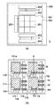
図1(a)に光電変換装置の平面配置図の一例を示す。光電変換装置1は画素回路201が配された画素回路部101と周辺回路(202〜204)が配された周辺回路部102とを含む。これら画素回路部101と周辺回路部102は単一の半導体基板100の上に設けられている。
FIG. 1A illustrates an example of a planar layout of the photoelectric conversion device. The
図1(b)に画素回路部101の4つの画素回路201に関する平面配置図の一例を示す。画素回路201は、光電変換素子PDと光電変換素子PDから信号を読み出す読み出し回路とからなる一つの単位である。このような画素回路201が複数配置されている領域が画素回路部101である。画素は、フォトダイオードなどの光電変換素子PD及びこの光電変換素子PDから出力線へ画像信号を読み出すための素子の集合の最小単位である。画素回路201は、光電変換素子PDで生じた電荷の量に基づく信号を生成する増幅素子SFを有する。このような光電変換装置1は、画素増幅型の撮像装置を構成できる。この素子集合に含まれるのは、例えば、転送素子TX、容量素子FD、増幅素子SF、リセット素子RSである。本例では、さらに、選択素子SLも素子集合に含まれる。隣接する光電変換素子PDにおいて、上記素子を共有することも可能であるが、この場合にも光電変換素子PDの信号を読み出すための素子集合の最小単位により画素を定義づけることができる。なお、位相差検出方式の焦点検出を実現するために、1つの画素に複数の光電変換素子PDを設け、画素からの信号を、複数の光電変換素子PDからの信号を合算したものとして扱うこともできる。
FIG. 1B shows an example of a plan layout diagram regarding the four
図1(a)に示すように、周辺回路部102には信号処理回路202、垂直シフトレジスタ203、水平シフトレジスタ204が含まれる。信号処理回路202は、画素回路201から読み出された信号の増幅や画素のノイズをCDS処理により除去する回路である。また2次元に配置された画素から行単位で複数並列に読み出された信号を、外部に出力するためにシリアルな信号に変換するための回路であっても良い。垂直シフトレジスタ203は画素回路部101に配された画素回路201を行単位で選択して、駆動するための駆動回路である。水平シフトレジスタ204は信号処理回路202を駆動して信号処理回路202から信号を外部に転送するための回路である。光電変換装置1においてAD変換を行なう場合には、AD変換回路が周辺回路に含まれても良い。
As shown in FIG. 1A, the
まず、本発明に係る光電変換装置1について図2により説明する。図2は図1(b)のA−B線における模式的断面図である。本実施例においては、画素回路部に配される素子としてフォトダイオードである光電変換素子PDとMOS型ゲートである転送素子TX、MOS型電界効果トランジスタ(MOSFET)である増幅素子を例に説明する。また各実施例においては特定の素子のみを例にあげて説明するが、画素回路201に配される他の素子に実施例の構造を適用することも可能である。画素回路201を構成するトランジスタを画素トランジスタと総称する。画素トランジスタは、MOS型電界効果トランジスタ(MOSFET)に限らず接合型電界効果トランジスタ(JFET)であってもよいし、バイポーラトランジスタであってもよい。一方、周辺回路を構成するトランジスタを周辺トランジスタと総称する。周辺トランジスタはMOS型電界効果トランジスタ(MOSFET、MOSトランジスタ)を含む。周辺回路部102には抵抗素子や容量素子など、MOSFET以外の素子を配することもできる。以下、MOS型電界効果トランジスタのことをMOSトランジスタと称する。なお、MOS型電界効果トランジスタは絶縁ゲート型電界効果トランジスタと同義であり、ゲート絶縁膜の種類は酸化膜に限定されることはない。
First, the
光電変換装置1は画素回路部101と周辺回路部102を含む。ここでは、画素回路部101のうち、光電変換素子PD、転送素子TX、増幅素子SFの断面構造を示している。そして、周辺回路部102に示されている周辺トランジスタは、信号処理回路202、垂直シフトレジスタ203、水平シフトレジスタ204、AD変換回路などのいずれかの回路を構成するものを示している。
The
シリコンなどの半導体基板100にSTIまたは選択酸化法(LOCOS)などにより形成された素子分離領域103が配置されている。画素回路部101には、転送MOSゲートのゲート電極111、増幅素子SFのゲート電極112が形成されている。第1導電型の不純物領域113は光電変換素子PDの蓄積領域として機能する。第1導電型は、光電変換素子PDが信号として取り扱う光電荷(信号電荷)を多数キャリアとする導電型に一致する導電型であり、信号電荷として電子を用いる場合にはN型となる。半導体基板100の表面と不純物領域113の間には光電変換素子PDを埋め込み構造とするための第2導電型の不純物領域118が形成されている。第2導電型は、第1導電型とは反対の導電型であり、信号電荷として電子を用いる場合にはP型となる。第1導電型の不純物領域114は容量素子FDの浮遊拡散領域として機能する。転送MOSゲートをゲート、不純物領域113をトランジスタのソース、不純物領域114をトランジスタのドレインとみなして、このトランジスタを転送トランジスタと称することもできる。第1導電型の不純物領域115は、シングルドレイン構造を有する増幅素子SFのドレインやソースを構成する。増幅素子のドレインには電源電位が与えられる。増幅素子SFのソースには選択素子SLを介して電流源が接続されており、増幅素子SFはソースフォロワ回路を構成している。不純物領域114はリセット素子RSのドレインに接続されている。また、不純物領域114は、増幅素子SFのゲート電極112に接続されている。リセット素子RSのソースにはリセット電位が与えられ、リセット素子RSのゲートをONにすることで、不純物領域114およびゲート電極112の電位がリセットされる。選択素子SLを用いずに増幅素子SFの電源電位を画素選択用の電位としてもよい。また、リセット電位と電源電位を共用してもよい。
An
第2導電型の不純物領域116には、第2導電型のウェル117の電位(ウェル電位)を規定するために基準となる電位が与えられる。ウェル電位は例えば接地電位である。不純物領域116はウェル電位を規定するためのウェルコンタクトの少なくとも一部を構成する。不純物領域116は、光電変換素子PDの信号電荷として電子を用いる場合にはウェル117と同じP型の不純物領域である。不純物領域116は素子分離領域103を構成する素子分離用の絶縁物で囲まれて形成されており、光電変換素子PDの活性領域や増幅素子SFの活性領域とは別の活性領域に形成されている。しかし、不純物領域116を光電変換素子PDの活性領域や増幅素子SFの活性領域と同じ活性領域に設けることもできる。1つの画素回路201につき1つのウェルコンタクトを設けることができるが、複数の画素回路201につき1つウェルコンタクトを設けることもできる。
The second conductivity
画素回路部101には、光電変換素子PDと増幅素子SFを覆う誘電体膜131aが設けられている。誘電体膜131aはさらに転送素子TX、容量素子FD(不純物領域114)、リセット素子RSおよび選択素子SLを覆っている。詳細には、誘電体膜131aは転送素子TXのゲート電極111の上面、増幅素子SFのゲート電極112の上面を覆っている。同様に誘電体膜131aは、リセット素子RSのゲート電極および選択素子SLのゲート電極を覆っている。酸化シリコン層および窒化シリコン層を含む複層膜から構成される誘電体膜131aは、両者で光電変換素子PDの表面での入射光の反射を低減する反射防止膜として機能することができる。なお、誘電体膜131aは窒化シリコン層と酸化シリコン層の組み合わせ以外の組み合わせの複層膜であってもよいし、単層膜であってもよい。誘電体膜131aは、不純物領域116の上に位置する開口130を有している。画素回路部101を覆う酸化シリコン層の単層膜である絶縁体膜132は、周辺回路部102においてシリサイド電極を形成する際にシリサイド、例えばコバルトシリサイドなどによる金属汚染から画素回路部101を保護する役割を果たす。絶縁体膜132は窒化シリコン層の単層膜であってもよいし、複層膜であってもよい。
The
周辺回路部102には、第1導電型のMOSトランジスタと第2導電型のMOSトランジスタを含む複数の周辺トランジスタが配されている。周辺回路部102において、第1導電型のMOSトランジスタ(NT)と第2導電型のMOSトランジスタ(PT)がCMOS回路を構成する場合もある。ゲート電極121は第1導電型の周辺トランジスタのゲート電極、ゲート電極122は第2導電型の周辺トランジスタのゲート電極である。周辺トランジスタはLDD構造を有する。すなわち、第1導電型の周辺トランジスタのソースとドレインは、第1導電型の不純物領域123と、不純物領域123よりも不純物濃度が低い第1導電型の不純物領域124とを含んで構成される。同様に、第2導電型の周辺トランジスタのソースとドレインは、第2導電型の不純物領域125と、不純物領域125よりも不純物濃度が低い第2導電型の不純物領域126とを含んで構成される。
The
ゲート電極121、122の側面には、酸化シリコン層と窒化シリコン層の積層体であるサイドスペーサ131bが形成されている。サイドスペーサ131bは酸化シリコン層と窒化シリコン層の積層膜をエッチングして残った残存物で形成されている。周辺トランジスタのゲート電極の表面とソースおよびドレインの表面はシリサイド化されている。シリサイド化には、たとえばコバルトシリサイドが用いられる。周辺回路部102を覆う酸化シリコン層と窒化シリコン層の積層膜である絶縁体膜135は窒化シリコン層、酸化シリコン層の組み合わせの複層膜に限らず、他の組み合わせの複層膜もしくは単層膜であってもよい。
絶縁膜133は、画素回路部101および周辺回路部102を覆う。絶縁膜133の上面は平坦である。絶縁膜133の上には不図示の配線層が設けられており、絶縁膜133はこの配線層に対する層間絶縁膜として機能する。画素回路部101には画素回路201の各素子の不純物領域やゲート電極に接続されたコンタクトプラグ141a等の導電体が設けられている。コンタクトプラグ141aは絶縁膜133、絶縁体膜132および誘電体膜131aを貫通して設けられている。誘電体膜131aは、コンタクトプラグ141aのためのコンタクトホールを形成する時のエッチングストッパとして機能する。周辺回路部102には周辺トランジスタの不純物領域やゲート電極に接続されたコンタクトプラグ141b等の導電体が設けられている。コンタクトプラグ141bは絶縁膜133および絶縁体膜135を貫通して設けられている。絶縁体膜135は、コンタクトプラグ141bのためのコンタクトホールを形成する時のエッチングストッパとして機能する。コンタクトプラグ141a、141bは、絶縁膜133のエッチングにより形成されたコンタクトホールにタングステンなどの導電体を充填して形成されている。画素回路部101の誘電体膜131aと、周辺回路部102のサイドスペーサ131bを形成する誘電体膜とを同じ構成とした場合には、誘電体膜を光電変換装置1の表面に一度に形成することができるので、製造コストを低く抑えることができる。
The insulating
画素回路部101のウェル117には第2導電型の不純物領域116が設けられている。ウェル117にはコンタクトプラグ141aを介して不純物領域116に基準電位(接地電位)が与えられる。画素回路部101にて基準電位を供給することで、画素回路201毎の基準電位のばらつきが低減され、シェーディングの発生を抑制することができる。また、MOSトランジスタのソースとドレインは低不純物濃度の不純物領域で構成されるシングルドレイン構造とする。このため、ソース、ドレインに高不純物濃度の不純物領域を含むLDD構造と比べ、ホットキャリアによるトランジスタ特性の劣化を低く抑えることができる。これは特に、MOSトランジスタが微細化された場合には顕著となる。ホットキャリアによるトランジスタ特性の劣化はゲート長と電源電圧に強く依存し、短いゲート長や高い電源電圧で劣化が大きくなる特性を持つ。本実施例による画素回路部のシングルドレイン構造のMOSトランジスタは、ゲート長が短い微細なMOSトランジスタであっても高い電源電圧で特性の劣化を抑えることができる。
A second conductivity
一方、周辺回路部102において、周辺トランジスタは高不純物濃度の不純物領域及び低不純物濃度の不純物領域からなるLDD構造のソース、ドレインを有するMOSトランジスタである。そのため、高駆動能力とホットキャリア耐性を両立させることができる。特に画素回路部と比べて周辺回路部においては、画素回路部よりも高速での動作が要求されるため、周辺トランジスタが高駆動能力を有することが重要となる。そのため、本実施例のように画素回路部のMOSトランジスタと周辺回路部のMOSトランジスタの電界緩和領域の構造を異ならせることが重要となる。
On the other hand, in the
また、画素回路部101の誘電体膜131aはコンタクトホールを開口する異方性ドライエッチングの際のエッチングストッパとして用いてもよい。これによりコンタクトが位置合わせずれにより素子分離領域上へ乗り上げた場合でも、コンタクトが素子分離領域や側面のウェル117と接触することが無い。このため低不純物濃度の不純物領域114、115とウェル117間のリーク電流を抑制できる。したがってコンタクトと素子分離領域との距離を短くすることができ、素子の微細化が可能となる。
In addition, the
次に、実施例に係る光電変換装置1の製造方法に関して説明する。図3(a)〜図5(i)に製造方法のフローを示す。尚、説明のため図3(a)〜図5(i)では画素回路部101と周辺回路部102を隣接させて描いている。
Next, a method for manufacturing the
まず、図3(a)の工程について説明する。シリコンなどの半導体基板100に、STIまたは選択酸化法(LOCOS)などにより素子分離領域103を形成する。また、半導体基板100に素子を形成するための第1導電型(N型)のウェル128、第2導電型(P型)のウェル117および127を形成する。画素を形成する画素回路部101には光電変換素子PDの第1導電型(N型)の不純物領域113を形成する。また、光電変換素子PDを埋め込み構造とするために、光電変換素子PDの表面に第2導電型(P型)の不純物領域118を形成する。また、半導体基板100の上にゲート電極111、112を形成する。さらに、容量素子FDを成す浮遊拡散領域(フローティング・ディフュージョン)としての不純物領域114、画素回路部101のシングルドレイン構造の増幅素子SFのソースやドレインとなる不純物領域115を形成する。このとき、ゲート電極111、112をマスクとして用いることができる。これにより増幅素子SFの第1導電型(N型)の低不純物濃度の不純物領域115が形成される。周辺回路部102には、周辺トランジスタとなるMOSトランジスタのゲート電極121、ゲート電極122を形成する。LDD構造となる領域に不純物を注入して、第1導電型の低不純物濃度の不純物領域124及び第2導電型の低不純物濃度の不純物領域126を形成する。このときもゲート電極121、122をマスクとして用いることができる。不純物領域114や不純物領域115、不純物領域124、不純物領域126の形成のためのドーズ量の適当な範囲は、5×1012〜5×1014[ions/cm2]であり、好ましくは1×1013〜1×1014[ions/cm2]である。ともに第1導電型である不純物領域114、115の形成のための不純物の注入と、不純物領域124、126の形成のための不純物の注入とを並行して行うことができる。
First, the process of FIG. 3A will be described. An
図3(a)に示す工程の次に、図3(b)に示すように、画素回路部101と周辺回路部102を覆う酸化シリコン層および窒化シリコン層の誘電体膜131を形成する。誘電体膜131は光電変換素子PD、増幅素子SF及び周辺トランジスタのゲート電極を覆う。誘電体膜131はさらに、リセット素子RS、選択素子SLなどの他の画素トランジスタや、転送素子TXのゲート電極111、容量素子FDの不純物領域114を覆う。積層膜としての誘電体膜131は、上層の窒化シリコン層を下層の酸化シリコン層よりも厚くした積層膜を用いることができる。例えば、先に厚みが5〜20nmの酸化シリコン層を熱CVD法で形成してから、厚みが20〜100nmの窒化シリコン層をプラズマCVD法で形成することができる。プラズマCVD法で形成した窒化シリコン層は水素を多量に含むことができるの。そのため、窒化シリコン層を形成した後に350°C以上の熱処理を施すことにより、上層の窒化シリコン層から放出され、下層の酸化シリコン層を透過した水素が、半導体基板100に拡散してダングリングボンドの終端化効果が得られる。これによりノイズを低減することができる。また、酸化シリコン層は窒化シリコン層の応力を緩和する層としても機能する。また、酸化シリコン層を形成することで、窒化シリコン層をプラズマCVD法で形成する際の半導体基板100へのプラズマダメージを低減することができる。
After the step shown in FIG. 3A, as shown in FIG. 3B, a
次に図3(c)に示すように、画素回路部101のウェル電位を規定する不純物領域116の上方に位置する部分を除く画素回路部上にレジスト150を形成し、酸化シリコン層および窒化シリコン層からなる誘電体膜131をエッチングする。レジスト150によって保護された、誘電体膜131の光電変換素子PD、増幅素子SFを覆う部分が、誘電体膜131aとして残存する。また、誘電体膜131のリセット素子RS、選択素子SLなどの他の画素トランジスタや、転送ゲートのゲート電極111、不純物領域114を覆う部分も誘電体膜131aとして残存する。一方、レジスト150で保護されない周辺回路部102では、ゲート電極121、122の側面に誘電体膜131の一部を残してエッチバックすることにより、誘電体膜131の残存物によりサイドスペーサ131bが形成される。サイドスペーサ131bとなる残存物は酸化シリコン層および窒化シリコン層の積層構造を維持している。このときにエッチングに伴って、画素回路部101において、誘電体膜131の一部をエッチングして開口130を形成する。この開口130の形成のために除去されるのは、誘電体膜131のウェルコンタクトの不純物領域116が形成される予定の区域の上方に位置する部分である。この後、ウェルコンタクトがこの開口130を介して形成される。サイドスペーサ131bの形成のためのエッチングと開口130の形成のためのエッチングとを並行して行うことで、半導体基板100へのダメージが抑制される。さらにこの時、光電変換素子PDや増幅素子SFなどの画素回路部101の素子の上で誘電体膜131をエッチングしないことで、これらの素子にエッチングダメージが加わることを避け、ノイズを低減することができる。特に光電変換素子PDや増幅素子SFへのエッチングダメージは暗電流や固定パターンノイズの原因となり得るため、このようにすることでノイズ特性に優れた光電変換装置を得ることができる。
Next, as shown in FIG. 3C, a resist 150 is formed on the pixel circuit portion excluding a portion located above the
次に図4(d)に示すように、レジスト160を画素回路部101と周辺回路部102に形成する。このとき、レジスト160は周辺回路部102の第1導電型(N型、NT)のMOSトランジスタの部分に開口を有するように形成する。そして、レジスト160及び、周辺回路部102の第1導電型(N型)のMOSトランジスタのゲート電極121とサイドスペーサ131bをマスクとして用い、第1導電型(N型)不純物を注入する。これによりサイドスペーサ131bの側面に自己整合した高不純物濃度のソース、ドレインの第1導電型の不純物領域123が形成される。
Next, as shown in FIG. 4D, a resist 160 is formed in the
同様に、図4(e)に示すように、画素回路部101の不純物領域116と周辺回路部102の第2導電型(P型、PT)のMOSトランジスタの部分に開口を有するようにレジスト170を形成する。次に、レジスト170及び、ゲート電極122とサイドスペーサ131bをマスクとして用い、第2導電型(P型)の不純物を注入する。この不純物の注入により、サイドスペーサ側面に自己整合したソース、ドレインの高不純物濃度の不純物領域125が形成される。このとき、並行して画素回路部101の不純物領域116にも第2導電型(P型)の不純物を、開口130を介してウェル117に注入することにより、ウェルコンタクトの不純物領域116を高不純物濃度の第2導電型の不純物領域として形成することができる。不純物領域123や不純物領域125、不純物領域116の形成のためのドーズ量の適当な範囲は、5×10¹⁴〜5×10¹⁶[ions/cm2]であり、好ましくは1×1015〜1×1016[ions/cm2]である。
Similarly, as shown in FIG. 4E, a resist 170 is formed so that an opening is formed in the
以上の工程により周辺回路部102のMOSトランジスタの構造をLDD構造にすると共に、ウェルコンタクトの不純物領域116の第2導電型の不純物濃度を高くすることができるので、不純物領域116のコンタクト抵抗を低くできる。ウェルコンタクトの不純物領域の形成のための不純物の注入と周辺回路部の第2導電型のMOSトランジスタのソースとドレインへの形成のための不純物の注入を同時に行っている。この後にアニール処理を行うこともできる。
Through the above steps, the structure of the MOS transistor in the
次に図4(f)に示すように、サリサイドプロセスにおいて画素回路部101を保護するための酸化シリコン層の単層膜である絶縁体膜132を画素回路部101に形成する。絶縁体膜132は開口130を覆うように形成されている。その後、周辺回路部102におけるMOSトランジスタのゲート電極上面にサリサイドにプロセスによるゲート電極のシリサイド化によって、コバルトシリサイド等のシリサイド層134を形成する。サリサイドプロセスによってシリサイド層134が画素回路部101に形成されるとシリサイド層134と半導体基板100の界面がノイズ源となり得る。しかし、開口130が絶縁体膜132で覆われた状態でサリサイドプロセスを行うことで、開口130の下に位置する半導体基板100の表面(不純物領域116の表面)がシリサイド化されることを回避できる。また周辺回路部102のMOSトランジスタのソース及びドレインの表面もコバルトなどによりシリサイド化する。次に、コンタクトホール形成時のエッチングストッパとして機能する酸化シリコン層および窒化シリコン層の積層膜である絶縁体膜135を周辺回路部102に形成する。絶縁体膜135はパターニングを経て周辺回路部102に形成され画素回路部101には形成されない。さらに、画素回路部101および周辺回路部102に渡ってBPSGなどのケイ酸塩ガラスやHDP−CVD法などで形成された酸化シリコンからなる絶縁膜133を全面に形成する。絶縁膜133の上面は、リフロー法、エッチバック法、CMP法などにより平坦化される。この段階までに、800℃を超えるアニール処理によりウェルコンタクトの不純物領域116に注入した不純物の熱拡散、活性化を行って、コンタクト抵抗をより低くできる。後述するコンタクトホールを形成した後では、このような高温のアニール処理を行うことが困難であるため、コンタクトホールを形成する前に高温のアニール処理を行うのがよい。
Next, as illustrated in FIG. 4F, an
次に図5(g)に示すように、画素回路部101と周辺回路部102を画素回路部101上に開口を有するレジスト180で覆う。画素回路部101の酸化シリコン層および窒化シリコン層からなる誘電体膜131aをエッチングストッパに用いて、コンタクトホール140aを異方性ドライエッチングにより開口する。画素回路部101にて形成された複数のコンタクトホール140aの一部は、絶縁膜133の不純物領域116の上に位置する部分に形成される。コンタクトホール140aの一部は開口130内に誘電体膜131aに囲まれた状態で形成されることになる。コンタクトホール140aの幅(径)は開口130の幅(径)よりも小さくすることができる。そして画素回路部101のコンタクトホール底部が接触する部分が各不純物領域に自己整合したコンタクトホールを形成する。またこのときコンタクトホール底部に露出する部分は金属配線による電気的な接続が可能な不純物濃度を確保することが望ましい。そのため、コンタクトホールを介して不純物領域116、114、115などに不純物を注入してもよい。コンタクトホール140aを介して不純物領域114、115に注入される不純物は不純物領域114、115と同じ第1導電型であることが好ましい。コンタクトホール140aを介して不純物領域116に注入される不純物は不純物領域116の導電型とは反対の第1導電型であってもよいし、第2導電型であってもよいし、この両方であってもよい。
Next, as illustrated in FIG. 5G, the
次に図5(h)に示すように、レジスト180を除去して、画素回路部101と周辺回路部102を周辺回路部102上に開口を有するレジスト190で覆う。レジスト190はコンタクトホール140aを覆う。次に、周辺回路部102の酸化シリコン層および窒化シリコン層からなる絶縁体膜135をエッチングストッパに用いて、周辺回路部102に異方性ドライエッチングによりコンタクトホール140bを開口する。続いてレジスト190を除去して、コンタクトホール140a、140bの中に導電体を充填してコンタクトプラグ141a、141bを形成する。こうして図5(i)に示すような光電変換装置1が得られる。ここでは、周辺回路部102のコンタクトホール140bを画素回路部101のコンタクトホール140aを形成した後に形成したが、コンタクトホール140bをコンタクトホール140aの前に形成してもよい。このようにコンタクトール140a、140bを別々に形成することで、シリサイド層134の金属による画素回路部101の不純物領域の金属汚染を低減できる。しかし、コンタクトホール140bとコンタクトホール140aを並行して形成してもよい。
Next, as shown in FIG. 5H, the resist 180 is removed, and the
周辺回路部102のサイドスペーサ131bをエッチバックにて形成する工程において、並行して、画素回路部101の不純物領域116の上方に位置する部分の誘電体膜131aをエッチバックして開口130を形成する。不純物領域116の上方に開口130を形成する工程をサイドスペーサ131bの形成と一緒に行っている。また、周辺回路部102の第2導電型のMOSトランジスタのソース、ドレインとすべき領域への不純物の注入と並行して、不純物領域116にも不純物を注入する。不純物領域116に不純物を注入する工程を他の注入工程と一緒に行うことができる。これにより、不純物領域116の形成を、BPSG等の絶縁膜133を形成してからコンタクトホールを開口して行う場合と比較して、工程を削減して製造コストを低く抑えることができる。さらには、不純物領域116に不純物を注入した後にアニール処理を加えることで不純物領域116は十分に活性化され、ウェル117と十分に接続され、コンタクトプラグ141aとの接触抵抗をより低くすることができる。ウェルコンタクトの抵抗を低くできるので、撮像面内での基準電位の一定化をさらに図ることが可能となり、シェーディングによる画像性能の低下を抑制することができる。
In the step of forming the
Claims (16)
前記光電変換素子、前記増幅素子、前記コンタクトが配される部分、及び前記MOSトランジスタのゲート電極を覆う誘電体膜を形成する工程と、
前記誘電体膜における前記光電変換素子を覆う部分と前記増幅素子を覆う部分とを覆い、前記周辺回路部分と前記コンタクトが配される部分とを露出させるレジストを形成する工程と、
前記誘電体膜における前記光電変換素子を覆う部分及び前記増幅素子を覆う部分をレジストによって保護して残存させつつ、前記ゲート電極の側面に前記誘電体膜の残存物によりサイドスペーサが形成され且つ前記コンタクトが配される部分の前記誘電体膜に開口が形成されるように、前記誘電体膜をエッチングする工程と、
を有し、
前記コンタクトを前記開口に形成することを特徴とする光電変換装置の製造方法。 A pixel circuit unit having a peripheral circuit unit including a MOS transistor, a well in which a photoelectric conversion element and an amplification element for amplifying a signal generated in the photoelectric conversion element are arranged, and a contact for supplying a predetermined voltage to the well A method of manufacturing a photoelectric conversion device comprising:
The photoelectric conversion element, said amplifying element, said portion of the contact is disposed, and forming a dielectric film covering the gate electrode of the MOS transistor,
Forming a resist covering a portion covering the photoelectric conversion element and a portion covering the amplifying element in the dielectric film, and exposing the peripheral circuit portion and the portion where the contact is disposed;
Said dielectric while remaining protected by the resist portion covering the portion and the amplifying element covering said photoelectric conversion elements in the membrane, the side spacer by remnants of the dielectric film is formed and the on the side surface of the gate electrode in so that an opening is formed on the dielectric film in a portion where the contact is disposed, a step of etching the dielectric film,
Have,
Method of manufacturing a photoelectric conversion device characterized by forming the contactor bets on the opening.
前記絶縁膜の前記不純物領域となる領域の上に位置する部分にコンタクトホールを形成し、前記コンタクトホールを介して前記領域に不純物を注入する段階を含むことを特徴とする請求項4に記載の光電変換装置の製造方法。 The contact is formed by forming an insulating film over the pixel circuit portion and the peripheral circuit portion on the dielectric film after the opening is formed,
5. The method according to claim 4, further comprising: forming a contact hole in a portion of the insulating film located on the region to be the impurity region, and implanting the impurity into the region through the contact hole. A method for manufacturing a photoelectric conversion device.
前記コンタクトは、平面視において、前記複数の光電変換素子の少なくとも2つの間にあることを特徴とする請求項1乃至15のいずれか1項に記載の光電変換装置の製造方法。 The method for manufacturing a photoelectric conversion device according to claim 1, wherein the contact is between at least two of the plurality of photoelectric conversion elements in a plan view.
Priority Applications (2)
| Application Number | Priority Date | Filing Date | Title |
|---|---|---|---|
| JP2013242363A JP6305030B2 (en) | 2013-11-22 | 2013-11-22 | Method for manufacturing photoelectric conversion device |
| US14/532,160 US9331121B2 (en) | 2013-11-22 | 2014-11-04 | Method of manufacturing photoelectric conversion apparatus including pixel well contact |
Applications Claiming Priority (1)
| Application Number | Priority Date | Filing Date | Title |
|---|---|---|---|
| JP2013242363A JP6305030B2 (en) | 2013-11-22 | 2013-11-22 | Method for manufacturing photoelectric conversion device |
Publications (3)
| Publication Number | Publication Date |
|---|---|
| JP2015103629A JP2015103629A (en) | 2015-06-04 |
| JP2015103629A5 JP2015103629A5 (en) | 2017-01-05 |
| JP6305030B2 true JP6305030B2 (en) | 2018-04-04 |
Family
ID=53183005
Family Applications (1)
| Application Number | Title | Priority Date | Filing Date |
|---|---|---|---|
| JP2013242363A Active JP6305030B2 (en) | 2013-11-22 | 2013-11-22 | Method for manufacturing photoelectric conversion device |
Country Status (2)
| Country | Link |
|---|---|
| US (1) | US9331121B2 (en) |
| JP (1) | JP6305030B2 (en) |
Families Citing this family (8)
| Publication number | Priority date | Publication date | Assignee | Title |
|---|---|---|---|---|
| JP6282109B2 (en) * | 2013-12-26 | 2018-02-21 | キヤノン株式会社 | Imaging device manufacturing method and imaging device |
| US9473719B2 (en) * | 2013-12-30 | 2016-10-18 | Taiwan Semiconductor Manufacturing Company, Ltd. | Protection layer in CMOS image sensor array region |
| US9608033B2 (en) | 2014-05-12 | 2017-03-28 | Canon Kabushiki Kaisha | Solid-state image sensor, method of manufacturing the same, and camera |
| JP6529221B2 (en) * | 2014-05-14 | 2019-06-12 | キヤノン株式会社 | Photoelectric conversion device and method of manufacturing the same |
| JP2016001709A (en) | 2014-06-12 | 2016-01-07 | キヤノン株式会社 | Solid state image pickup device manufacturing method |
| JP6789653B2 (en) | 2016-03-31 | 2020-11-25 | キヤノン株式会社 | Photoelectric converter and camera |
| JP6991739B2 (en) * | 2017-05-12 | 2022-01-13 | キヤノン株式会社 | Manufacturing method of semiconductor device |
| JP7059336B2 (en) * | 2020-11-04 | 2022-04-25 | キヤノン株式会社 | Photoelectric converters and cameras |
Family Cites Families (11)
| Publication number | Priority date | Publication date | Assignee | Title |
|---|---|---|---|---|
| JP3664968B2 (en) | 1999-12-01 | 2005-06-29 | イノテック株式会社 | Solid-state imaging device, manufacturing method thereof, and solid-state imaging device |
| US6504194B1 (en) | 1999-12-01 | 2003-01-07 | Innotech Corporation | Solid state imaging device, method of manufacturing the same, and solid state imaging system |
| JP3467013B2 (en) | 1999-12-06 | 2003-11-17 | キヤノン株式会社 | Solid-state imaging device |
| JP2005302836A (en) * | 2004-04-07 | 2005-10-27 | Matsushita Electric Ind Co Ltd | Method for manufacturing solid-state imaging device |
| JP2006041080A (en) | 2004-07-26 | 2006-02-09 | Sony Corp | Solid-state imaging apparatus |
| JP4424120B2 (en) * | 2004-08-31 | 2010-03-03 | ソニー株式会社 | Solid-state imaging device and method for manufacturing solid-state imaging device |
| JP4756839B2 (en) | 2004-09-01 | 2011-08-24 | キヤノン株式会社 | Solid-state imaging device and camera |
| JP5110820B2 (en) * | 2006-08-02 | 2012-12-26 | キヤノン株式会社 | Photoelectric conversion device, photoelectric conversion device manufacturing method, and imaging system |
| JP5558916B2 (en) * | 2009-06-26 | 2014-07-23 | キヤノン株式会社 | Method for manufacturing photoelectric conversion device |
| JP5564874B2 (en) | 2009-09-25 | 2014-08-06 | ソニー株式会社 | Solid-state imaging device and electronic apparatus |
| US8878264B2 (en) * | 2011-04-26 | 2014-11-04 | Aptina Imaging Corporation | Global shutter pixel with improved efficiency |
-
2013
- 2013-11-22 JP JP2013242363A patent/JP6305030B2/en active Active
-
2014
- 2014-11-04 US US14/532,160 patent/US9331121B2/en not_active Expired - Fee Related
Also Published As
| Publication number | Publication date |
|---|---|
| US9331121B2 (en) | 2016-05-03 |
| US20150147843A1 (en) | 2015-05-28 |
| JP2015103629A (en) | 2015-06-04 |
Similar Documents
| Publication | Publication Date | Title |
|---|---|---|
| JP6282109B2 (en) | Imaging device manufacturing method and imaging device | |
| JP6305030B2 (en) | Method for manufacturing photoelectric conversion device | |
| JP5110820B2 (en) | Photoelectric conversion device, photoelectric conversion device manufacturing method, and imaging system | |
| US8952433B2 (en) | Solid-state image sensor, method of manufacturing the same, and imaging system | |
| JP6179865B2 (en) | Solid-state imaging device and manufacturing method thereof | |
| JP6529221B2 (en) | Photoelectric conversion device and method of manufacturing the same | |
| JP2015109343A (en) | Method of manufacturing semiconductor device | |
| JP2008060356A (en) | Photoelectric conversion device, and imaging system | |
| WO2014002362A1 (en) | Solid-state image pickup apparatus and method for manufacturing same | |
| KR20070007666A (en) | Image sensor and methods of fabricating the same | |
| TWI648841B (en) | Semiconductor device manufacturing method | |
| JP2018041836A (en) | Solid-state imaging device, method of manufacturing the same, and camera | |
| JP6346488B2 (en) | Semiconductor device, solid-state imaging device, manufacturing method thereof, and camera | |
| JP6681150B2 (en) | Solid-state imaging device, manufacturing method thereof, and camera | |
| US20160126284A1 (en) | Solid-state imaging device and method of manufacturing solid-state imaging device | |
| US20160156817A1 (en) | Manufacturing method of imaging apparatus, imaging apparatus, and imaging system | |
| JP2019067826A (en) | Imaging apparatus, method of manufacturing the same, and apparatus | |
| JP6341796B2 (en) | Manufacturing method of semiconductor device | |
| JP5355740B2 (en) | Method for manufacturing photoelectric conversion device | |
| JP2012146989A (en) | Photoelectric conversion device and imaging system | |
| JP2009176950A (en) | Solid-state image sensor and method of manufacturing the same process | |
| KR101024825B1 (en) | Image sensor and Manufacturing method of image sensor | |
| JP4115446B2 (en) | Manufacturing method of CMOS image sensor | |
| JP2015046505A (en) | Semiconductor device and manufacturing method of the same | |
| WO2013018308A1 (en) | Method for manufacturing solid-state imaging device |
Legal Events
| Date | Code | Title | Description |
|---|---|---|---|
| A521 | Request for written amendment filed |
Free format text: JAPANESE INTERMEDIATE CODE: A523 Effective date: 20161117 |
|
| A621 | Written request for application examination |
Free format text: JAPANESE INTERMEDIATE CODE: A621 Effective date: 20161117 |
|
| A131 | Notification of reasons for refusal |
Free format text: JAPANESE INTERMEDIATE CODE: A131 Effective date: 20170721 |
|
| A977 | Report on retrieval |
Free format text: JAPANESE INTERMEDIATE CODE: A971007 Effective date: 20170720 |
|
| A521 | Request for written amendment filed |
Free format text: JAPANESE INTERMEDIATE CODE: A523 Effective date: 20170919 |
|
| TRDD | Decision of grant or rejection written | ||
| A01 | Written decision to grant a patent or to grant a registration (utility model) |
Free format text: JAPANESE INTERMEDIATE CODE: A01 Effective date: 20180205 |
|
| A61 | First payment of annual fees (during grant procedure) |
Free format text: JAPANESE INTERMEDIATE CODE: A61 Effective date: 20180306 |
|
| R151 | Written notification of patent or utility model registration |
Ref document number: 6305030 Country of ref document: JP Free format text: JAPANESE INTERMEDIATE CODE: R151 |