JP7433863B2 - Photoelectric conversion devices, imaging systems, and mobile objects - Google Patents
Photoelectric conversion devices, imaging systems, and mobile objects Download PDFInfo
- Publication number
- JP7433863B2 JP7433863B2 JP2019214776A JP2019214776A JP7433863B2 JP 7433863 B2 JP7433863 B2 JP 7433863B2 JP 2019214776 A JP2019214776 A JP 2019214776A JP 2019214776 A JP2019214776 A JP 2019214776A JP 7433863 B2 JP7433863 B2 JP 7433863B2
- Authority
- JP
- Japan
- Prior art keywords
- photoelectric conversion
- well
- signal
- pixel
- transistor
- Prior art date
- Legal status (The legal status is an assumption and is not a legal conclusion. Google has not performed a legal analysis and makes no representation as to the accuracy of the status listed.)
- Active
Links
- 238000006243 chemical reaction Methods 0.000 title claims description 65
- 238000003384 imaging method Methods 0.000 title claims description 37
- 239000004065 semiconductor Substances 0.000 claims description 34
- 239000000758 substrate Substances 0.000 claims description 31
- 230000003321 amplification Effects 0.000 claims description 30
- 238000003199 nucleic acid amplification method Methods 0.000 claims description 30
- 239000012212 insulator Substances 0.000 claims description 26
- 238000000926 separation method Methods 0.000 claims description 19
- 238000012545 processing Methods 0.000 claims description 11
- 238000009792 diffusion process Methods 0.000 claims description 8
- 238000000034 method Methods 0.000 claims description 2
- 230000000149 penetrating effect Effects 0.000 claims description 2
- 239000000969 carrier Substances 0.000 claims 1
- 238000010586 diagram Methods 0.000 description 32
- 238000002955 isolation Methods 0.000 description 30
- 230000000694 effects Effects 0.000 description 10
- 230000006866 deterioration Effects 0.000 description 9
- 102100036285 25-hydroxyvitamin D-1 alpha hydroxylase, mitochondrial Human genes 0.000 description 4
- 101000875403 Homo sapiens 25-hydroxyvitamin D-1 alpha hydroxylase, mitochondrial Proteins 0.000 description 4
- 230000006870 function Effects 0.000 description 4
- 238000005259 measurement Methods 0.000 description 4
- 238000012546 transfer Methods 0.000 description 4
- 125000003345 AMP group Chemical group 0.000 description 3
- 230000000052 comparative effect Effects 0.000 description 3
- 238000001514 detection method Methods 0.000 description 3
- 229920006227 ethylene-grafted-maleic anhydride Polymers 0.000 description 3
- 230000003287 optical effect Effects 0.000 description 3
- XUIMIQQOPSSXEZ-UHFFFAOYSA-N Silicon Chemical compound [Si] XUIMIQQOPSSXEZ-UHFFFAOYSA-N 0.000 description 2
- 230000004888 barrier function Effects 0.000 description 2
- 230000008859 change Effects 0.000 description 2
- 239000000470 constituent Substances 0.000 description 2
- 239000012535 impurity Substances 0.000 description 2
- 230000009467 reduction Effects 0.000 description 2
- 229910052710 silicon Inorganic materials 0.000 description 2
- 239000010703 silicon Substances 0.000 description 2
- 230000000295 complement effect Effects 0.000 description 1
- 238000012937 correction Methods 0.000 description 1
- 238000009413 insulation Methods 0.000 description 1
- 239000000463 material Substances 0.000 description 1
- 230000007246 mechanism Effects 0.000 description 1
- 229910044991 metal oxide Inorganic materials 0.000 description 1
- 150000004706 metal oxides Chemical class 0.000 description 1
- 238000012986 modification Methods 0.000 description 1
- 230000004048 modification Effects 0.000 description 1
Images


Classifications
-
- H—ELECTRICITY
- H01—ELECTRIC ELEMENTS
- H01L—SEMICONDUCTOR DEVICES NOT COVERED BY CLASS H10
- H01L27/00—Devices consisting of a plurality of semiconductor or other solid-state components formed in or on a common substrate
- H01L27/14—Devices consisting of a plurality of semiconductor or other solid-state components formed in or on a common substrate including semiconductor components sensitive to infrared radiation, light, electromagnetic radiation of shorter wavelength or corpuscular radiation and specially adapted either for the conversion of the energy of such radiation into electrical energy or for the control of electrical energy by such radiation
- H01L27/144—Devices controlled by radiation
- H01L27/146—Imager structures
- H01L27/14601—Structural or functional details thereof
- H01L27/14609—Pixel-elements with integrated switching, control, storage or amplification elements
- H01L27/14612—Pixel-elements with integrated switching, control, storage or amplification elements involving a transistor
-
- H—ELECTRICITY
- H01—ELECTRIC ELEMENTS
- H01L—SEMICONDUCTOR DEVICES NOT COVERED BY CLASS H10
- H01L27/00—Devices consisting of a plurality of semiconductor or other solid-state components formed in or on a common substrate
- H01L27/14—Devices consisting of a plurality of semiconductor or other solid-state components formed in or on a common substrate including semiconductor components sensitive to infrared radiation, light, electromagnetic radiation of shorter wavelength or corpuscular radiation and specially adapted either for the conversion of the energy of such radiation into electrical energy or for the control of electrical energy by such radiation
- H01L27/144—Devices controlled by radiation
- H01L27/146—Imager structures
- H01L27/14601—Structural or functional details thereof
- H01L27/14609—Pixel-elements with integrated switching, control, storage or amplification elements
-
- H—ELECTRICITY
- H01—ELECTRIC ELEMENTS
- H01L—SEMICONDUCTOR DEVICES NOT COVERED BY CLASS H10
- H01L31/00—Semiconductor devices sensitive to infrared radiation, light, electromagnetic radiation of shorter wavelength or corpuscular radiation and specially adapted either for the conversion of the energy of such radiation into electrical energy or for the control of electrical energy by such radiation; Processes or apparatus specially adapted for the manufacture or treatment thereof or of parts thereof; Details thereof
- H01L31/02—Details
- H01L31/02016—Circuit arrangements of general character for the devices
- H01L31/02019—Circuit arrangements of general character for the devices for devices characterised by at least one potential jump barrier or surface barrier
-
- H—ELECTRICITY
- H01—ELECTRIC ELEMENTS
- H01L—SEMICONDUCTOR DEVICES NOT COVERED BY CLASS H10
- H01L31/00—Semiconductor devices sensitive to infrared radiation, light, electromagnetic radiation of shorter wavelength or corpuscular radiation and specially adapted either for the conversion of the energy of such radiation into electrical energy or for the control of electrical energy by such radiation; Processes or apparatus specially adapted for the manufacture or treatment thereof or of parts thereof; Details thereof
- H01L31/08—Semiconductor devices sensitive to infrared radiation, light, electromagnetic radiation of shorter wavelength or corpuscular radiation and specially adapted either for the conversion of the energy of such radiation into electrical energy or for the control of electrical energy by such radiation; Processes or apparatus specially adapted for the manufacture or treatment thereof or of parts thereof; Details thereof in which radiation controls flow of current through the device, e.g. photoresistors
- H01L31/10—Semiconductor devices sensitive to infrared radiation, light, electromagnetic radiation of shorter wavelength or corpuscular radiation and specially adapted either for the conversion of the energy of such radiation into electrical energy or for the control of electrical energy by such radiation; Processes or apparatus specially adapted for the manufacture or treatment thereof or of parts thereof; Details thereof in which radiation controls flow of current through the device, e.g. photoresistors characterised by at least one potential-jump barrier or surface barrier, e.g. phototransistors
- H01L31/101—Devices sensitive to infrared, visible or ultraviolet radiation
-
- B—PERFORMING OPERATIONS; TRANSPORTING
- B60—VEHICLES IN GENERAL
- B60R—VEHICLES, VEHICLE FITTINGS, OR VEHICLE PARTS, NOT OTHERWISE PROVIDED FOR
- B60R11/00—Arrangements for holding or mounting articles, not otherwise provided for
- B60R11/04—Mounting of cameras operative during drive; Arrangement of controls thereof relative to the vehicle
Description
本発明は、光電変換装置、撮像システム、及び移動体に関する。 The present invention relates to a photoelectric conversion device, an imaging system, and a moving object.
増幅トランジスタ(以下、AMP)を含む画素を備える光電変換装置が知られている。AMPの基板バイアス効果による信号の線形性の劣化を抑制するためには、AMPを含むウェル(第1ウェル)とAMPのソースを接続する必要がある。また、第1ウェルを光電変換部から分離する必要がある。特許文献1には、AMPが配されるP型の第1ウェルと光電変換部が配されるP型の第2ウェルとの分離部として、トレンチとN型の分離層とを用いることが開示されている。具体的には、第1ウェルと第2ウェルとの間にトレンチが配され、第1ウェルの下部にN型の分離層が配されることが開示され、トレンチとN型の分離層とで第1ウェルと第2ウェルとが分離されている。
2. Description of the Related Art A photoelectric conversion device including a pixel including an amplification transistor (hereinafter referred to as AMP) is known. In order to suppress deterioration in signal linearity due to the substrate bias effect of the AMP, it is necessary to connect the well containing the AMP (first well) to the source of the AMP. Furthermore, it is necessary to separate the first well from the photoelectric conversion section.
特許文献1において、第1ウェルと第2ウェルとを分離し、AMPからの信号の線形性の劣化を抑制するためには、N型の分離層に所定の電圧を印加する必要がある。しかしながら、特許文献1では、分離層への電圧の印加ができず、第1ウェルと第2ウェルとの分離が不十分になる可能性がある。分離層に電圧を印加しようとするとトレンチが形成されている側の面までN型半導体領域が配置されている必要がある。しかしながら、N型半導体領域が配されると、画素に対する第1ウェルと第2ウェルとの分離部の面積が大きくなり、光電変換部の面積を確保しにくくなる可能性がある。
In
本発明の目的は、小さい面積で増幅トランジスタが配されたウェルと光電変換部とを分離しつつ、増幅トランジスタ効果の基板バイアス効果による信号の線形性の劣化を抑制することである。 An object of the present invention is to suppress deterioration of signal linearity due to the substrate bias effect of the amplification transistor effect while separating a well in which an amplification transistor is arranged and a photoelectric conversion section in a small area.
本発明の一形態に係る光電変換装置は、半導体基板と、前記半導体基板内に設けられた光電変換部と、前記光電変換部からの信号を出力する増幅トランジスタと、平面視で、前記増幅トランジスタを取り囲んで、前記光電変換部と前記増幅トランジスタとの間に配され、前記半導体基板を貫通する絶縁体分離部と、を備え、前記増幅トランジスタが配される第1ウェルと、前記増幅トランジスタのソースまたはドレインと、が接続されている。 A photoelectric conversion device according to one embodiment of the present invention includes a semiconductor substrate, a photoelectric conversion section provided in the semiconductor substrate, an amplification transistor that outputs a signal from the photoelectric conversion section, and, in a plan view, the amplification transistor an insulating isolation part surrounding the photoelectric conversion part and the amplification transistor and penetrating the semiconductor substrate, a first well in which the amplification transistor is arranged; The source or drain is connected.
本発明の光電変換装置によれば、小さい面積で増幅トランジスタが配されたウェルと光電変換部とを分離しつつ、増幅トランジスタの基板バイアス効果による信号の線形性の劣化を抑制することができる。 According to the photoelectric conversion device of the present invention, deterioration in signal linearity due to the substrate bias effect of the amplification transistor can be suppressed while separating the photoelectric conversion section from the well in which the amplification transistor is arranged in a small area.
以下、図面を参照しながら本発明の実施形態について説明する。なお以下の実施形態は、いずれも本発明の一例を示すのであり、数値、形状、材料、構成要素、構成要素の配置および接続形態などは、本発明を限定するものではない。また、以下で説明する図面において、同じ機能を有するものは同一の符号を付し、その説明を省略、又は簡潔にすることがある。 Embodiments of the present invention will be described below with reference to the drawings. Note that the following embodiments are all examples of the present invention, and the numerical values, shapes, materials, constituent elements, arrangement of constituent elements, connection forms, etc. do not limit the present invention. Furthermore, in the drawings described below, parts having the same functions are denoted by the same reference numerals, and the description thereof may be omitted or simplified.
本発明は、以下の実施の形態に限らず種々の変形が可能である。例えば、いずれかの実施の形態の一部の構成を他の実施の形態に追加した例や、他の実施の形態の一部の構成と置換した例も、本発明の実施の形態である。すなわち、本発明はその技術思想、又はその主要な特徴から逸脱することなく、様々な態様で実施することができる。 The present invention is not limited to the following embodiments, and various modifications are possible. For example, an example in which a part of the configuration of any embodiment is added to another embodiment, or an example in which a part of the configuration in another embodiment is replaced are also embodiments of the present invention. That is, the present invention can be implemented in various embodiments without departing from its technical idea or its main features.
以下の説明では、信号キャリアと同じキャリアを多数キャリアとする第1導電型の半導体領域がN型半導体領域であり、第2導電型の半導体領域がP型半導体領域である。つまり、信号キャリアが電子である。なお、導電型が全て逆であってもよい。つまり、信号キャリアが正孔であり、第1導電型の半導体領域がP型半導体領域、第2導電型の半導体領域がN型半導体領域であってもよい。 In the following description, a semiconductor region of a first conductivity type whose majority carrier is the same carrier as a signal carrier is an N-type semiconductor region, and a semiconductor region of a second conductivity type is a P-type semiconductor region. In other words, the signal carrier is an electron. Note that the conductivity types may all be reversed. That is, the signal carrier may be a hole, the first conductivity type semiconductor region may be a P type semiconductor region, and the second conductivity type semiconductor region may be an N type semiconductor region.
(実施形態1)
図1~図5を用いて、本発明の実施形態1に係る光電変換装置について説明する。
(Embodiment 1)
A photoelectric conversion device according to
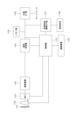
図1は光電変換装置の構成例を概略的に示すブロック図である。光電変換装置100は、画素アレイ部101、定電流源部111、アナログデジタル(AD)変換部121、垂直走査回路131、水平走査回路141、出力部151からなる。
FIG. 1 is a block diagram schematically showing a configuration example of a photoelectric conversion device. The
画素アレイ部101は、複数の画素102が2次元アレイ状に配置されている。垂直走査回路131に選択された所定の画素行に位置する画素の信号電圧が出力線104に読み出される。図1では、出力線104は、画素列毎に1つ設けられている。これに限らず、出力線は、画素列毎に複数設けられていてもよいし、複数の画素列毎に1つ設けられていてもよい。
In the
定電流源部111は、出力線104毎に配置された定電流源回路112からなる。定電流源回路112は、画素102に含まれる増幅トランジスタと電気的に接続されている。
The constant
AD変換部121は、複数のAD変換回路122からなる。複数のAD変換回路122は、出力線104毎に配置されている。出力線104に出力された信号電圧を、AD変換部121でデジタル変換してデジタル信号を保持する。その後、水平走査回路141により、順次、デジタル信号を、出力部151を介して光電変換装置100の外部へと出力する。この動作を垂直走査回路131で選択行を走査しながら繰り返し行うことで、2次元の画像データが生成される。
The
図2は、本実施形態における画素102の等価回路図である。
FIG. 2 is an equivalent circuit diagram of the
画素102は、光電変換部を構成するフォトダイオード(PD)201、浮遊拡散部(FD)202、転送トランジスタ(TX)203、リセットトランジスタ(RES)204、選択トランジスタ(SEL)205、増幅トランジスタ(AMP)206により構成される。AMP206が配されたウェルWAMPは、他のトランジスタが配されたウェルと電気的に分離され、AMP206のソースと電気的に接続されている。以下では、AMP206としてソースフォロワトランジスタを用いる場合について説明するが、AMP206の構成はこれに限定されない。例えばAMP206はソース接地の増幅トランジスタであってもよい。なお、画素102において、SEL205およびRES204は必須ではない。画素102は、複数のPD201を含み、複数のPD201がAMPを共有してもよい。また、画素102は、複数のPD201、および複数のAMP206を含んでいてもよい。
The
図3を用いて、本実施形態の画素のレイアウトを示す。図3は、図2の等価回路図に対応した画素を含むレイアウトであり、平面視で2行×2列の計4つの画素を示している。図3の横方向がXまたはY方向であり、紙面に対して奥行に向かう方向がZ方向である。本明細書において「平面視」とは、半導体基板のトランジスタのゲートが配されている側の面と平行な面を該平行な面に対して垂直方向から視ることを指す。つまり、「平面視」とは、図3において、半導体基板の第1面に平行な面に対してZ方向又は-Z方向から視ることを指す。図3において、紙面左上の画素を画素1、左下の画素を画素2、右上の画素を画素3、右下の画素を画素4とする。本明細書中では、画素1のPD201を201-1、画素2のPD201を201-2のように、画素mのPD201を201-mと示す。他の素子も同様である。また、各画素において素子の構成が共通である場合は、mを省略して説明する。例えば、各画素のPD201が共通の構成を備える場合は、201―mのmを省略して201と記載して説明する。
The pixel layout of this embodiment is shown using FIG. 3. FIG. 3 is a layout including pixels corresponding to the equivalent circuit diagram of FIG. 2, and shows a total of four pixels in two rows and two columns in plan view. The horizontal direction in FIG. 3 is the X or Y direction, and the direction toward the depth of the page is the Z direction. In this specification, "planar view" refers to a surface parallel to a surface of a semiconductor substrate on which a gate of a transistor is disposed, as viewed from a direction perpendicular to the parallel surface. In other words, "planar view" refers to viewing from the Z direction or -Z direction with respect to a plane parallel to the first surface of the semiconductor substrate in FIG. In FIG. 3, the pixel at the top left of the page is
画素は、平面視で、絶縁体分離部DTIにより少なくとも2つの領域に分離されている。一方の領域にAMP206が配され、他方の領域にPD201が配される。平面視で、AMP206とPD201との間には絶縁体分離部DTIが配されている。絶縁体分離部DTIは、AMP206を取り囲むように配されている。絶縁体分離部DTIは、AMP206のチャネルとなる領域を含むウェルWAMPと、PD201が配されたウェルWPDとを分離する機能をもつ。図3では、絶縁体分離部DTIは、画素間のPD201が配されたウェルWPD間も分離しているが、画素間におけるウェルWPD間は分離されていなくてもよい。
The pixel is separated into at least two regions by the insulator isolation portion DTI in plan view. The AMP 206 is placed in one area, and the
ウェルWAMPは、ウェルWAMPに配されたAMPウェルコンタクトWCAMPを介してAMP206のソースと電気的に接続されている。ウェルWPDは、ウェルWPDに配されたPDウェルコンタクトWCPDを介して接地電圧と電気的に接続されている。TX203、RES204、SEL205はそれぞれウェルWPDに配されている。つまり、AMP206と、RES204およびSEL205と、の間には、絶縁体分離部DTIが配されている。
The well W AMP is electrically connected to the source of the
図4は、図3のA-A’の概略断面図である。半導体基板301において、AMP206のゲートとなる電極206Gが配されている側の面を第1面S1といい、第1面S1に対向する面を第2面S2という。第1面S1から第2面S2に向かう方向がZ方向である。図4では、第2面S2から光が入射する。第2面S2を裏面と呼び、第1面S1を表面と呼ぶこともある。半導体基板としては、例えば、シリコン基板や、SOI(Silicon on Insulator)基板を用いることができる。
FIG. 4 is a schematic cross-sectional view taken along line A-A' in FIG. In the
FD202、TX203、RES204、AMP206等の画素トランジスタのソース、ドレインはN型の不純物が拡散されたN型半導体領域により構成される。AMP206のゲートとなる電極206G、TX203のゲートとなる電極203Gは、第1面S1に配される。ウェルWAMPのウェルコンタクトWCAMPと、ウェルWPDのウェルコンタクトWCPDと、は、半導体基板301内に配され、それぞれP型の不純物が拡散されたP型半導体領域により構成される。ウェルコンタクトWCAMPとウェルコンタクトWCPDとは、半導体基板301の第1面S1の一部を構成する。各トランジスタの間には、素子分離部305が配される。素子分離部305はSTI構造あるいはLOCOS構造により構成されている。図4に示すように、Z方向において、絶縁体分離部DTIは、半導体基板301を貫通している。半導体基板301内において、AMP206のチャネルとなる領域を含むウェルWAMPとPD201を含むウェルWPDとが絶縁体分離部DTIで電気的に分離されている。
The sources and drains of pixel transistors such as the
絶縁体分離部DTIは、図4に示すように、幅が変わっていてもよい。例えば、Z方向に絶縁体分離部DTIの幅が狭くなっていてもよい。また、第1面S1と第2面S2とを結ぶ線の中点における幅よりも、第1面S1を通る仮想平面における絶縁体分離部DTIの幅や第2面S2を通る仮想平面における絶縁体分離部DTIにおける幅が広くてもよい。言い換えると、絶縁体分離部DTIはZ方向に向かって、第1の幅の部分と、第1の幅よりも幅の狭い第2の幅の部分と、第2の幅よりも幅の広い第3の部分と、を順に有していてもよい。第1面S1と第2面S2の双方から貫通孔を形成する場合は、後者のように、中点における幅と仮想平面における幅とで幅が変わることがある。 The width of the insulator isolation portion DTI may vary as shown in FIG. 4. For example, the width of the insulator isolation portion DTI may be narrowed in the Z direction. Furthermore, the width of the insulator separation portion DTI in the virtual plane passing through the first surface S1 and the insulation in the virtual plane passing through the second surface S2 are larger than the width at the midpoint of the line connecting the first surface S1 and the second surface S2. The width at the body separation portion DTI may be wide. In other words, the insulator isolation part DTI has a first width part, a second width part narrower than the first width, and a second width part wider than the second width in the Z direction. 3, and 3 in this order. When a through hole is formed from both the first surface S1 and the second surface S2, as in the latter case, the width may vary between the width at the midpoint and the width at the virtual plane.
絶縁体分離部DTIのXまたはY方向の幅は、0.5μm程度である。ウェルWAMPとウェルWPDとの電気的な分離を行う方法として、PN接合による分離も可能であるが、その場合、ウェルWAMPとウェルWPDの分離部に4.0μm程度の幅が必要となる。また、特許文献1のように、絶縁体分離部とPN接合分離とにより、ウェルWAMPとウェルWPDとを分離すると、PN分離のように幅が必要となる、あるいは、ウェル同士が電気的に分離されなくなる可能性がある。
The width of the insulator isolation portion DTI in the X or Y direction is approximately 0.5 μm. As a method for electrically isolating well W AMP and well W PD , separation using a PN junction is also possible, but in that case, a width of about 4.0 μm is required for the separation part between well W AMP and well W PD . becomes. Furthermore, as in
本実施形態によれば、半導体基板301を貫通する絶縁体分離部DTIによりウェルWAMPとPDとは物理的に分離されている。つまり、ウェルWAMPとウェルWPDとは絶縁体分離部DTIにより物理的に分離される。これにより、特許文献1やPN接合分離を用いる場合に比べて、ウェルWAMPとウェルWPDとの分離部に必要な面積を小さくしながら、ウェルWAMPとウェルWPDとを電気的に分離することができる。
According to this embodiment, the wells WAMP and PD are physically separated by the insulator isolation portion DTI that penetrates the
図5は、本実施形態における画素の信号読み出しを説明する駆動タイミング図である。本明細書中では、図5の時刻t401~時刻t405のように、各タイミングを時刻t401のように示す。φTXはTX203のオン/オフを示しており、φRESはRES204のオン/オフを示しており、φSELはSEL205のオン/オフを示している。各トランジスタにおいて、オン時はHighレベルで示し、オフ時はLowレベルで示す。VFDはFD202の電圧の変化の様子を示しており、VOUTは、出力線104の電圧の変化の様子を示している。以下、図5のタイミング図に沿って画素の信号読み出しの動作を説明する。
FIG. 5 is a drive timing diagram illustrating pixel signal readout in this embodiment. In this specification, each timing is indicated as time t 401 , such as time t 401 to time t 405 in FIG. φTX indicates on/off of
まず、時刻t401にSEL205をオンにして、AMP206のソースと出力線104を接続し、定電流源回路112によりAMP206に一定の電流を流す。AMP206のゲート-ソース間電圧VGSは、定電流源回路112で決められた一定の電流に対応した電圧となる。ソースと接続されているVOUTはゲートに接続されているVFDに対応した電圧となる。
First, at time t401 , the
時刻t402にRES204をオフにして、FD202をフローティングにする。その後、時刻t402から時刻t403の間に、VOUTをAD変換回路122でデジタル信号に変換する。ここで得られた信号をN信号と呼称する。
At time t402 , the
時刻t403にTX203をオンし、時刻t404にTX203をオフする。時刻t403から時刻t404に、PD201に蓄積した信号電荷をFD202に転送する。その後、SEL205をオフにするまでの時刻t404から時刻t405の間に、VOUTの電圧をAD変換回路122でデジタル信号に変換する。ここで得られた信号をN+S信号と呼称する。
At time t 403 ,
このようにして得られたN信号とN+S信号の差分を計算することで、PD201で生成された信号電荷の電荷量に対応した信号が得られる。
By calculating the difference between the N signal and the N+S signal obtained in this way, a signal corresponding to the amount of signal charges generated by the
ここで、AMP206のウェル電圧が信号の線形性に与える影響について、図15(A)、図15(B)、図16(A)、および図16(B)を参照しながら説明する。図15(A)および図15(B)は比較の実施形態を説明するための図であり、図16(A)および図16(B)は本実施形態を説明するための図である。AD変換時におけるAMP206のVGSは、概ね以下に示す(式1)から求めることができる。
Here, the influence of the well voltage of the

ここで、Iconstは定電流源回路112により決まる一定電流、WはAMP206のゲート幅、LはAMP206のゲート長、μはAMP206のチャネル電子の移動度、COXはAMP206の単位面積当たりの容量、VTHは閾値電圧である。
Here, I const is a constant current determined by the constant
また、閾値電圧VTHは、概ね以下に示す(式2)から求めることができる。 Further, the threshold voltage V TH can be approximately determined from (Equation 2) shown below.

VBSはバックバイアス(ウェル-ソース間電圧)、VTH0はVBSが0V時の閾値電圧、2φFは表面ポテンシャル、γは基板効果パラメータである。 V BS is a back bias (well-source voltage), V TH0 is a threshold voltage when V BS is 0 V, 2φ F is a surface potential, and γ is a substrate effect parameter.
図15(A)および図15(B)に示すように、比較の実施形態では、ウェルWAMPとウェルWPDとが分離されておらず、ウェルWAMPが接地されている。比較の実施形態では、VBSが変化するため、閾値電圧VTHが非線形に変化し、AMP206に一定電流Iconstが流れていても、ゲート-ソース間電圧VGSが一定とならない。そのため、FD202の電圧変化に対する出力線104の電圧変化が非線形となってしまう。このように、ウェルWAMPとウェルWPDとが分離されておらず、ウェルWAMPが接地されている場合は、出力信号電圧によりVBSが変化するため、信号の線形性が劣化する。
As shown in FIGS. 15(A) and 15(B), in the comparative embodiment, well W AMP and well W PD are not separated, and well W AMP is grounded. In the comparative embodiment, as V BS changes, the threshold voltage V TH changes non-linearly, and the gate-source voltage V GS is not constant even though a constant current I const is flowing through the
図16(A)および図16(B)に示すように、本実施形態では、ウェルWAMPを、ウェルWPDと物理的に分離し、AMP206のソースとウェルWPDを電気的に接続しているためVBSは0Vで固定される。そのため、AMP206のVTHを一定にすることができる。したがって、信号の線形性が非線形とならない。
As shown in FIGS. 16(A) and 16(B), in this embodiment, the well W AMP is physically separated from the well W PD , and the source of the
以上の説明の通り、本実施形態では、基板バイアス効果による信号の線形性の劣化を抑制することができる。 As described above, in this embodiment, deterioration in signal linearity due to the substrate bias effect can be suppressed.
上述の通り、本実施形態によれば、PN接合分離と比較して小さい体積でウェルWAMPとウェルWPDとを分離し、基板バイアス効果による信号の線形性の劣化を抑制することができる。 As described above, according to this embodiment, the well W AMP and the well W PD can be separated with a smaller volume than PN junction separation, and deterioration of signal linearity due to the substrate bias effect can be suppressed.
(実施形態2)
図6、図7を用いて、本発明の実施形態2に係る画素について説明する。本実施形態は、画素が、複数のPD201と複数のTX203を含み、複数のPD201がFD202を共有している点が実施形態1とは異なる。以下、実施形態1と同様の構成は説明を省略し、異なる構成を中心に説明する。
(Embodiment 2)
A pixel according to
図6は、本実施形態における画素の等価回路図である。PD201とTX203がそれぞれ2つずつ配置されている。以下では、1つの画素に含まれる複数の構成にはそれぞれA、B…と付する。例えば、1つの画素が複数のPD201を含む場合は、あるPDをPD201Aといい、あるPDとは異なるPDをPD201Bという。
FIG. 6 is an equivalent circuit diagram of a pixel in this embodiment. Two
本実施形態は、図6に示すように、PD201AとTX203A、PD201BとTX203Bで、FD202、RES204、SEL205、AMP206からなる読み出し回路を共有している。
In this embodiment, as shown in FIG. 6, the
図7は、図6に示す画素が1行2列に配されたレイアウト図である。図7に示すように、1つの画素が、2行×1列に配されたPD201を含む。紙面左側の垂直2つのPDを有する画素を画素1、右側の縦2つのPDを有する画素を画素2とする。画素2は画素1と同様の素子を有する。
FIG. 7 is a layout diagram in which the pixels shown in FIG. 6 are arranged in one row and two columns. As shown in FIG. 7, one pixel includes
本実施形態によれば、実施形態1よりもPDあたりの絶縁体分離部DTIの数を減らし、より小さい体積でウェルWAMPとウェルWPDとを分離し、基板バイアス効果による信号の線形性の劣化を抑制することができる。 According to the present embodiment, the number of insulator isolation parts DTI per PD is reduced compared to the first embodiment, the well W AMP and the well W PD are separated with a smaller volume, and the linearity of the signal due to the substrate bias effect is improved. Deterioration can be suppressed.
(実施形態3)
図8~図10を用いて、本発明の実施形態3に係る画素について説明する。本実施形態は、複数のAMPがSELを共有している点が実施形態2とは異なる。以下、実施形態2と同様の構成は説明を省略し、異なる構成を中心に説明する。
(Embodiment 3)
A pixel according to Embodiment 3 of the present invention will be explained using FIGS. 8 to 10. This embodiment differs from the second embodiment in that a plurality of AMPs share an SEL. Hereinafter, explanations of configurations similar to those in
図8は、本実施形態における画素102の等価回路図である。図8では2つの画素102を示している。各画素には、光電変換部PD201と転送トランジスタTX203が2つずつ配置されている。また、浮遊拡散部FD、リセットトランジスタRES、および増幅トランジスタAMPが1つずつ配置されている。画素1のAMP206-1と画素2のAMP206-2とにより選択トランジスタSEL205が共有されている。AMP206-1のドレイン電圧VDD1とAMP206-2のドレイン電圧VDD2は、それぞれ独立に電圧制御が可能になっている。
FIG. 8 is an equivalent circuit diagram of the
図9は、画素のレイアウト図である。図9は2つの画素を示しており、2行×2列の光電変換部PDの範囲で示している。図9に示すように、半導体基板を貫通する絶縁体分離部DTIに囲まれた領域に、画素1のAMP206-1と画素2のAMP206-2とが配されている。つまり、AMP206-1のソースとAMP206-2のソースはウェルWPDから分離された同一のウェルWAMPに接続されている。
FIG. 9 is a pixel layout diagram. FIG. 9 shows two pixels, which are shown in the range of the photoelectric conversion unit PD of 2 rows and 2 columns. As shown in FIG. 9, the AMP 206-1 of the
本実施形態では、同一のウェルWAMPに複数のAMPを配置し、シリアルに駆動することで、ウェル分離の数を少なくしつつ、電荷電圧変換係数の縮小を抑制している。 In this embodiment, by arranging a plurality of AMPs in the same well W AMP and driving them serially, reduction in the charge-voltage conversion coefficient is suppressed while reducing the number of well separations.
図10は、本実施形態における画素の信号読み出しを説明する駆動タイミング図である。以下、図10のタイミング図に沿って画素の信号読み出しの動作を説明する。 FIG. 10 is a drive timing diagram illustrating pixel signal readout in this embodiment. The pixel signal readout operation will be described below with reference to the timing diagram of FIG. 10.
まず、時刻t901でSEL205をオンにして、AMP206-1とAMP206-2のソースと出力線104を接続する。このとき、VDD1を高い電圧とし、VDD2を低い電圧とする。AMP206-2のゲートにはVDD2の低い電圧が印加されるため、電流は、AMP206-1から定電流源回路112へと流れ、VOUTはFD202-1に対応した電圧となる。
First, at time t 901 , the
時刻t902に、RES204-1をオフにして、FD202-1をフローティングにする。時刻t902から時刻t903の間に、VOUTをAD変換回路122でデジタル信号に変換する。ここで得られた信号をN1信号と呼称する。
At time t 902 , the RES 204-1 is turned off and the FD 202-1 is made floating. Between time t 902 and time t 903 , V OUT is converted into a digital signal by the
時刻t903にTX203A-1をオンし、時刻t904にオフする。時刻t903から時刻t904の期間にPD201A-1に保持された電荷をFD202-1に転送する。時刻t904から時刻t905の間にFD202-1から出力線104に出力された信号電圧VOUTをAD変換回路122でデジタル信号に変換する。ここで得られた信号をN1+S1信号と呼称する。
The TX203A-1 is turned on at time t903 and turned off at time t904 . The charges held in the
時刻t905にTX203B-1をオンし、時刻t906にオフする。時刻t907から時刻t908の期間にPD201B-1に保持された電荷をFD202-1に転送する。時刻t906から時刻t907の間にFD202-1から出力線104に出力された信号電圧VOUTをAD変換回路122でデジタル信号に変換する。ここで得られた信号をN1+S1+S2信号と呼称する。
The TX203B-1 is turned on at time t905 and turned off at time t906 . The charges held in the
時刻t907に、RES204-1をオンにする。このとき、VDD1を低い電圧とし、VDD2を高い電圧とする。AMP206-1のゲートにはVDD1の低い電圧が印加されるため、電流は、AMP206-2から定電流源回路112へと流れ、VOUTはFD202-2に対応した電圧となる。
At time t 907 , RES 204-1 is turned on. At this time, VDD1 is set to a low voltage and VDD2 is set to a high voltage. Since a low voltage of VDD1 is applied to the gate of the AMP 206-1, current flows from the AMP 206-2 to the constant
時刻t908に、RES204-2をオフにして、FD202-2をフローティングにする。時刻t908から時刻t909の間に、FD202-2から出力線104に出力された信号電圧VOUTをAD変換回路122でデジタル信号に変換する。ここで得られた信号をN2信号と呼称する。
At time t 908 , the RES 204-2 is turned off and the FD 202-2 is made floating. Between time t 908 and time t 909 , the signal voltage V OUT output from the FD 202-2 to the
時刻t909にTX203A-2をオンし、時刻t910にTX203A-2をオフする。時刻t909から時刻t910の期間にPD201A-2に保持された電荷をFD202-2に転送する。時刻t910から時刻t911の間にFD202-2から出力線104に出力された信号電圧VOUTをAD変換回路122でデジタル信号に変換する。ここで得られた信号をN2+S3信号と呼称する。
The TX203A-2 is turned on at time t909 , and the TX203A-2 is turned off at time t910 . The charges held in the
時刻t911にTX203B-2をオンし、時刻t912にTX203B-2をオフする。時刻t911から時刻t912の期間にPD201B-2に保持された電荷をFD202-Bに転送する。時刻t912から時刻t913の間にFD202-Bから出力線104に出力された信号電圧VOUTをAD変換回路122でデジタル信号に変換する。ここで得られた信号をN2+S3+S4信号と呼称する。
The TX203B-2 is turned on at time t911 , and the TX203B-2 is turned off at time t912 . The charges held in the
このようにして得られたN1信号とN1+S1信号の差分からPD201A-1で光電変換された信号電荷の電荷量に対応したS1信号が得られる。また、N1+S1信号とN1+S1+S2信号の差分からPD201B-1で光電変換された信号電荷の電荷量に対応したS2信号が得られる。また、N2信号とN2+S3信号の差分からPD201A-2で光電変換された信号電荷の電荷量に対応したS3信号が得られる。また、N2+S3信号とN2+S3+S4信号の差分からPD201B-2で光電変換された信号電荷の電荷量に対応したS4信号が得られる。
From the difference between the N1 signal and the N1+S1 signal thus obtained, an S1 signal corresponding to the amount of signal charge photoelectrically converted by the
本実施形態によれば、実施形態2よりもPDあたりのウェル分離の数を減らし、より小さい体積で基板バイアス効果による信号の線形性の劣化を抑制するとともに、電荷電圧変換係数の縮小を抑制することができる。
According to this embodiment, the number of well separations per PD is reduced compared to
(実施形態4)
図11、図12を用いて、本発明の実施形態4に係る画素について説明する。本実施形態は、1つの画素が2つの光電変換部PDを含む点が実施形態1とは異なる。以下、実施形態1と同様の構成は説明を省略し、異なる構成を中心に説明する。
(Embodiment 4)
A pixel according to Embodiment 4 of the present invention will be described using FIGS. 11 and 12. This embodiment differs from
図11は、本実施形態における画素102の等価回路図である。図11は、2つの画素102の等価回路図を示す。各画素102が2つの光電変換部PDと、2つの転送トランジスタとを含む。また、2つの画素が、浮遊拡散部FD202、リセットトランジスタRES204、増幅トランジスタAMP206、選択トランジスタSEL205を共有する。
FIG. 11 is an equivalent circuit diagram of the
図11は、画素の平面レイアウト図であり、2行×2列の画素を示す。前述の通り、各画素は2つの光電変換部PDを含む。紙面左上の画素を画素1、右上の画素を画素2、左下の画素を画素3、右下の画素を画素4とする。
FIG. 11 is a plan layout diagram of pixels, showing pixels arranged in two rows and two columns. As described above, each pixel includes two photoelectric conversion units PD. The pixel at the top left of the page is
各画素の光電変換部PD201AとPD201Bの間は、絶縁体からなる素子分離部305を介さずにPN接合分離で分離されている。画素内に含まれる複数の光電変換部PDによりマイクロレンズMLが共有されている。つまり、1つのマイクロレンズMLを通った光が、画素内の一方の光電変換部PDAと他方の光電変換部PDBとに入射するようにマイクロレンズMLは配される。PDAの出力信号群からなるA像、PDBの出力信号群からなるB像を元に、位相差検出方式による測距あるいは焦点検出が可能となる。
The photoelectric conversion units PD201A and PD201B of each pixel are separated by PN junction isolation without intervening an
本実施形態によれば、位相差検出画素において、基板バイアス効果による信号の線形性の劣化を抑制することができる。 According to this embodiment, it is possible to suppress deterioration of signal linearity due to the substrate bias effect in the phase difference detection pixel.
(実施形態5)
図13は本実施形態における撮像システムのブロック図である。撮像システムは、デジタルスチルカメラ、デジタルカムコーダ、カメラヘッド、監視用カメラ、複写機、ファックス、携帯端末、スマートフォン、車載カメラ、観測衛星、人口知能ロボットなどであり得る。本実施形態における撮像装置1100は、実施形態1から実施形態4の光電変換装置である。
(Embodiment 5)
FIG. 13 is a block diagram of the imaging system in this embodiment. The imaging system may be a digital still camera, a digital camcorder, a camera head, a surveillance camera, a copier, a fax machine, a mobile terminal, a smartphone, a vehicle-mounted camera, an observation satellite, an artificially intelligent robot, or the like. The
図13に示す撮像システムは、バリア1101、レンズ1102、絞り1103、撮像装置1100、信号処理部1104を有する。更に、撮像システムは、メモリ部1105、外部I/F部1106、記録媒体制御I/F部1107、記録媒体1108、機械装置1109、制御部1110を備える。バリア1101はレンズ1102を保護し、レンズ1102は被写体の光学像を撮像装置1100に結像させる。絞り1103はレンズ1102を通った光量を可変する。撮像装置1100はCMOS(Complementary Metal Oxide Semiconductor)型の光電変換装置であって、レンズ1102により結像された光学像を画像データに変換する。撮像装置1100は、画素回路、信号処理回路などが形成された半導体基板、半導体基板を格納するパッケージ、外部回路との接続端子などを含み得る。信号処理部1104は撮像装置1100より出力された画像データにおいて階調補正、ノイズ除去などの画像処理を行う。
The imaging system shown in FIG. 13 includes a
メモリ部1105はダイナミックメモリなどの揮発性メモリ、またはフラッシュメモリなどの不揮発性メモリを備え、画像データを格納するフレームメモリとして機能する。外部I/F部1106は外部コンピュータ、ネットワーク、サーバ等と通信するための有線または無線のインターフェースである。記録媒体制御I/F部1107は記録媒体1108に画像データの記録または読み出しを行うためのインターフェースであり、記録媒体1108は画像データを格納するための半導体メモリを有するメモリカード等の着脱可能な記録媒体である。機械装置1109はレンズ1102、絞り1103などの光学機構の駆動装置、カメラヘッドの姿勢制御などを行う機構装置などを含み得る。制御部1110はCPU、ROM、RAMなどを備え、予め定められたプログラムに従い、撮像システム全体の制御を行う。また、制御部1110は、画像データにおける被写体の動きを検出し、所定の処理を実行することが可能である。図10において、信号処理部1104、メモリ部1105、制御部1110は撮像装置1100とは別に設けられているが、撮像装置1100と同一の半導体基板に形成されてもよい。
The
(実施形態6)
図14(A)、図14(B)は、実施形態1~実施形態4における光電変換装置を車戴カメラに関する撮像システムに適用した例を示している。本実施形態において、撮像装置2010は実施形態1~実施形態4の光電変換装置に相当する。
(Embodiment 6)
14(A) and 14(B) show an example in which the photoelectric conversion device according to
撮像システム2000は、撮像装置2010により取得された複数の画像データに対し、画像処理を行う画像処理部2030と、撮像システム2000により取得された複数の画像データから視差(視差画像の位相差)の算出を行う視差算出部2040を有する。また、撮像システム2000は、算出された視差に基づいて対象物までの距離を算出する距離計測部2050と、算出された距離に基づいて衝突可能性があるか否かを判定する衝突判定部2060とを有する。ここで、視差算出部2040、距離計測部2050は、対象物までの距離情報を取得する距離情報取得手段の一例である。すなわち、距離情報とは、視差、デフォーカス量、対象物までの距離等に関する情報である。衝突判定部2060はこれらの距離情報のいずれかを用いて、衝突可能性を判定してもよい。距離情報取得手段は、専用に設計されたハードウェアによって実現されてもよいし、ソフトウェアモジュールによって実現されてもよい。また、FPGA(Field Programmable Gate Array)、ASIC(Application Specific Integrated Circuit)によって実現されてもよいし、これらの組合せによって実現されてもよい。
The
撮像システム2000は車両情報取得装置2310と接続されており、車速、ヨーレート、舵角などの車両情報を取得することができる。また、撮像システム2000は、衝突判定部2060での判定結果に基づいて、車両に対して制動力を発生させる制御信号を出力する制御装置である制御ECU2410が接続されている。また、撮像システム2000は、衝突判定部2060での判定結果に基づいて、ドライバーへ警報を発する警報装置2420とも接続されている。例えば、衝突判定部2060の判定結果として衝突可能性が高い場合、制御ECU2410はブレーキをかける、アクセルを戻す、エンジン出力を抑制するなどして衝突を回避、被害を軽減する車両制御を行う。警報装置2420は音等の警報を鳴らす、カーナビゲーションシステムなどの画面に警報情報を表示する、シートベルトまたはステアリングに振動を与えるなどしてユーザに警告を行う。撮像システム2000は上述のように車両を制御する動作の制御を行う制御手段として機能する。
The
本実施形態では車両の周囲、例えば前方または後方を撮像システム2000で撮像する。図11(B)に、車両前方(撮像範囲2510)を撮像する場合の撮像システムを示す。撮像制御手段としての車両情報取得装置2310が、撮像システム2000ないしは撮像装置2010に指示を送る。このような構成により、測距の精度をより向上させることができる。
In this embodiment, the
上述では、他の車両と衝突しないように制御する例を説明したが、他の車両に追従して自動運転する制御、車線からはみ出さないように自動運転する制御などにも適用可能である。さらに、撮像システムは、自車両等の車両に限らず、例えば、船舶、航空機あるいは産業用ロボットなどの移動体(移動装置)に適用することができる。加えて、移動体に限らず、高度道路交通システム(ITS)等、広く物体認識を利用する機器に適用することができる。 In the above, an example of control to avoid collision with other vehicles has been described, but it is also applicable to control to automatically drive while following other vehicles, control to automatically drive to avoid running out of the lane, etc. Furthermore, the imaging system can be applied not only to vehicles such as own vehicle, but also to mobile objects (mobile devices) such as ships, aircraft, and industrial robots. In addition, the present invention can be applied not only to mobile objects but also to a wide range of devices that use object recognition, such as intelligent transportation systems (ITS).
100 光電変換装置
102 画素
201 光電変換部(PD)
202 浮遊拡散部(FD)
203 転送トランジスタ(TX)
204 リセットトランジスタ(RES)
205 選択トランジスタ(SEL)
206 増幅トランジスタ(AMP)
301 半導体基板
DTI 絶縁体分離部
WAMP AMPが配されるウェル
WPD PDが配されるウェル
100
202 Floating diffusion section (FD)
203 Transfer transistor (TX)
204 Reset transistor (RES)
205 Selection transistor (SEL)
206 Amplification transistor (AMP)
301 Semiconductor substrate DTI Insulator isolation part W AMP Well where AMP is placed W PD Well where PD is placed
Claims (9)
前記半導体基板内に設けられた光電変換部と、前記光電変換部で生成された信号キャリアが転送される浮遊拡散部と、前記光電変換部からの信号を出力する増幅トランジスタと、前記浮遊拡散部に接続されるリセットトランジスタと、前記増幅トランジスタと出力線とに接続される選択トランジスタと、
平面視で、前記増幅トランジスタを取り囲んで、前記光電変換部と前記増幅トランジスタとの間に配され、前記半導体基板を貫通する絶縁体分離部と、を備え、
前記増幅トランジスタが配される第1ウェルと、前記リセットトランジスタと前記選択トランジスタとが配される第2ウェルと、を有し、
前記第1ウェルと、前記増幅トランジスタのソースまたはドレインと、が接続されており、
前記絶縁体分離部は、前記増幅トランジスタと前記リセットトランジスタとの間に配されていることを特徴とする光電変換装置。 a semiconductor substrate;
A photoelectric conversion section provided in the semiconductor substrate, a floating diffusion section to which signal carriers generated in the photoelectric conversion section are transferred, an amplification transistor that outputs a signal from the photoelectric conversion section, and the floating diffusion section . a reset transistor connected to the amplification transistor and a selection transistor connected to the output line;
an insulator separation part surrounding the amplification transistor, disposed between the photoelectric conversion part and the amplification transistor, and penetrating the semiconductor substrate in a plan view;
a first well in which the amplification transistor is disposed, and a second well in which the reset transistor and the selection transistor are disposed;
The first well and the source or drain of the amplification transistor are connected,
The photoelectric conversion device is characterized in that the insulator separation section is disposed between the amplification transistor and the reset transistor .
前記第1ウェルと前記増幅トランジスタのソースとが接続されていることを特徴とする請求項1に記載の光電変換装置。 The amplification transistor is a source follower transistor,
The photoelectric conversion device according to claim 1, wherein the first well and the source of the amplification transistor are connected.
前記第2ウェルと前記第1ウェルとの間に前記絶縁体分離部が配されていることを特徴とする請求項1または2に記載の光電変換装置。 The photoelectric conversion section is arranged in the second well,
3. The photoelectric conversion device according to claim 1, wherein the insulator separation section is arranged between the second well and the first well.
前記増幅トランジスタと前記浮遊拡散部との間に前記絶縁体分離部が配されることを特徴とする請求項1乃至3のいずれか1項に記載の光電変換装置。 the floating diffusion section is arranged in the second well,
4. The photoelectric conversion device according to claim 1 , wherein the insulator separation section is arranged between the amplification transistor and the floating diffusion section.
前記光電変換装置から出力される信号を処理する信号処理部と、を有することを特徴とする撮像システム。 A photoelectric conversion device according to any one of claims 1 to 7,
An imaging system comprising: a signal processing unit that processes a signal output from the photoelectric conversion device.
請求項1乃至7のいずれか1項に記載の光電変換装置と、
前記光電変換装置からの信号に基づく視差画像から、対象物までの距離情報を取得する距離情報取得手段と、
前記距離情報に基づいて前記移動体を制御する制御手段と、を有することを特徴とする移動体。 A mobile object,
A photoelectric conversion device according to any one of claims 1 to 7,
distance information acquisition means for acquiring distance information to a target object from a parallax image based on a signal from the photoelectric conversion device;
A moving object, comprising: a control means for controlling the moving object based on the distance information.
Priority Applications (2)
| Application Number | Priority Date | Filing Date | Title |
|---|---|---|---|
| JP2019214776A JP7433863B2 (en) | 2019-11-27 | 2019-11-27 | Photoelectric conversion devices, imaging systems, and mobile objects |
| US17/103,160 US20210159258A1 (en) | 2019-11-27 | 2020-11-24 | Photoelectric conversion device, imaging system, and movable body |
Applications Claiming Priority (1)
| Application Number | Priority Date | Filing Date | Title |
|---|---|---|---|
| JP2019214776A JP7433863B2 (en) | 2019-11-27 | 2019-11-27 | Photoelectric conversion devices, imaging systems, and mobile objects |
Publications (2)
| Publication Number | Publication Date |
|---|---|
| JP2021086919A JP2021086919A (en) | 2021-06-03 |
| JP7433863B2 true JP7433863B2 (en) | 2024-02-20 |
Family
ID=75975062
Family Applications (1)
| Application Number | Title | Priority Date | Filing Date |
|---|---|---|---|
| JP2019214776A Active JP7433863B2 (en) | 2019-11-27 | 2019-11-27 | Photoelectric conversion devices, imaging systems, and mobile objects |
Country Status (2)
| Country | Link |
|---|---|
| US (1) | US20210159258A1 (en) |
| JP (1) | JP7433863B2 (en) |
Families Citing this family (1)
| Publication number | Priority date | Publication date | Assignee | Title |
|---|---|---|---|---|
| JP7336320B2 (en) * | 2019-09-04 | 2023-08-31 | キヤノン株式会社 | IMAGING DEVICE AND CONTROL METHOD THEREOF, PROGRAM, STORAGE MEDIUM |
Citations (7)
| Publication number | Priority date | Publication date | Assignee | Title |
|---|---|---|---|---|
| JP2001160619A (en) | 1999-12-01 | 2001-06-12 | Victor Co Of Japan Ltd | Cmos image sensor and method of manufacturing the same |
| JP2010028423A (en) | 2008-07-18 | 2010-02-04 | Sony Corp | Solid-state imaging element and camera system |
| JP2011119441A (en) | 2009-12-03 | 2011-06-16 | Sony Corp | Imaging element and camera system |
| JP2013118273A (en) | 2011-12-02 | 2013-06-13 | Sony Corp | Amplifying circuit and manufacturing method, solid-state imaging element, and electronic device |
| JP2016005068A (en) | 2014-06-16 | 2016-01-12 | ソニー株式会社 | Solid-state imaging device and electronic apparatus |
| JP2017183661A (en) | 2016-03-31 | 2017-10-05 | キヤノン株式会社 | Photoelectric converter and camera |
| JP2019165136A (en) | 2018-03-20 | 2019-09-26 | ソニーセミコンダクタソリューションズ株式会社 | Solid state imaging device, manufacturing method therefor, and electronic apparatus |
Family Cites Families (28)
| Publication number | Priority date | Publication date | Assignee | Title |
|---|---|---|---|---|
| US6657665B1 (en) * | 1998-12-31 | 2003-12-02 | Eastman Kodak Company | Active Pixel Sensor with wired floating diffusions and shared amplifier |
| DE602004021974D1 (en) * | 2004-07-20 | 2009-08-20 | Fujitsu Microelectronics Ltd | CMOS IMAGE SENSOR ELEMENT |
| US7964929B2 (en) * | 2007-08-23 | 2011-06-21 | Aptina Imaging Corporation | Method and apparatus providing imager pixels with shared pixel components |
| US8115154B2 (en) * | 2008-08-01 | 2012-02-14 | Sony Corporation | Solid-state imaging device, method of producing the same, and imaging device |
| FR2950504B1 (en) * | 2009-09-24 | 2012-06-22 | St Microelectronics Sa | PICTURE SENSOR PIXEL CIRCUIT |
| FR2955701A1 (en) * | 2010-01-28 | 2011-07-29 | St Microelectronics Sa | COMPACT IMAGE SENSOR STRUCTURE |
| US9355888B2 (en) * | 2012-10-01 | 2016-05-31 | Taiwan Semiconductor Manufacturing Company, Ltd. | Implant isolated devices and method for forming the same |
| KR102366416B1 (en) * | 2014-08-11 | 2022-02-23 | 삼성전자주식회사 | CMOS image sensor |
| WO2017056346A1 (en) * | 2015-09-29 | 2017-04-06 | パナソニック・タワージャズセミコンダクター株式会社 | Solid-state imaging device |
| KR102466904B1 (en) * | 2016-01-12 | 2022-11-15 | 삼성전자주식회사 | CMOS image sensor |
| KR102541701B1 (en) * | 2016-01-15 | 2023-06-13 | 삼성전자주식회사 | CMOS Image Sensor |
| JP6612139B2 (en) * | 2016-01-22 | 2019-11-27 | ルネサスエレクトロニクス株式会社 | Semiconductor device |
| TW202310384A (en) * | 2016-01-27 | 2023-03-01 | 日商新力股份有限公司 | Solid-state image pickup device and electronic apparatus |
| JP6808348B2 (en) * | 2016-04-28 | 2021-01-06 | キヤノン株式会社 | Photoelectric converter and camera |
| KR20180078418A (en) * | 2016-12-29 | 2018-07-10 | 삼성전자주식회사 | Image sensor |
| KR102638779B1 (en) * | 2017-01-03 | 2024-02-22 | 삼성전자주식회사 | Image sensor |
| JP7193907B2 (en) * | 2017-01-23 | 2022-12-21 | キヤノン株式会社 | Solid-state imaging device |
| JP6929671B2 (en) * | 2017-03-17 | 2021-09-01 | キヤノン株式会社 | Imaging device and imaging system |
| US11044387B2 (en) * | 2017-03-24 | 2021-06-22 | Sony Semiconductor Solutions Corporation | Stacked imaging device and solid-state imaging apparatus |
| JP2018170543A (en) * | 2017-03-29 | 2018-11-01 | ソニーセミコンダクタソリューションズ株式会社 | Solid-state image capture device, electronic apparatus, and drive method |
| WO2019111373A1 (en) * | 2017-12-07 | 2019-06-13 | オリンパス株式会社 | Solid state imaging device and solid state imaging device production method |
| US10790326B2 (en) * | 2018-09-26 | 2020-09-29 | Taiwan Semiconductor Manufacturing Company, Ltd. | Pixel device on deep trench isolation (DTI) structure for image sensor |
| JP2020068289A (en) * | 2018-10-24 | 2020-04-30 | キヤノン株式会社 | Photoelectric conversion device, imaging system, mobile body, and semiconductor chip for lamination |
| KR102637626B1 (en) * | 2019-01-08 | 2024-02-20 | 삼성전자주식회사 | Image sensor |
| KR20200105138A (en) * | 2019-02-28 | 2020-09-07 | 삼성전자주식회사 | Semiconductor device including support region and method of forming the same |
| KR20200126477A (en) * | 2019-04-29 | 2020-11-09 | 삼성전자주식회사 | Image sensor |
| JP7286445B2 (en) * | 2019-06-28 | 2023-06-05 | キヤノン株式会社 | Imaging devices and equipment |
| US11437416B2 (en) * | 2019-09-10 | 2022-09-06 | Taiwan Semiconductor Manufacturing Company, Ltd. | Pixel device layout to reduce pixel noise |
-
2019
- 2019-11-27 JP JP2019214776A patent/JP7433863B2/en active Active
-
2020
- 2020-11-24 US US17/103,160 patent/US20210159258A1/en active Pending
Patent Citations (7)
| Publication number | Priority date | Publication date | Assignee | Title |
|---|---|---|---|---|
| JP2001160619A (en) | 1999-12-01 | 2001-06-12 | Victor Co Of Japan Ltd | Cmos image sensor and method of manufacturing the same |
| JP2010028423A (en) | 2008-07-18 | 2010-02-04 | Sony Corp | Solid-state imaging element and camera system |
| JP2011119441A (en) | 2009-12-03 | 2011-06-16 | Sony Corp | Imaging element and camera system |
| JP2013118273A (en) | 2011-12-02 | 2013-06-13 | Sony Corp | Amplifying circuit and manufacturing method, solid-state imaging element, and electronic device |
| JP2016005068A (en) | 2014-06-16 | 2016-01-12 | ソニー株式会社 | Solid-state imaging device and electronic apparatus |
| JP2017183661A (en) | 2016-03-31 | 2017-10-05 | キヤノン株式会社 | Photoelectric converter and camera |
| JP2019165136A (en) | 2018-03-20 | 2019-09-26 | ソニーセミコンダクタソリューションズ株式会社 | Solid state imaging device, manufacturing method therefor, and electronic apparatus |
Also Published As
| Publication number | Publication date |
|---|---|
| US20210159258A1 (en) | 2021-05-27 |
| JP2021086919A (en) | 2021-06-03 |
Similar Documents
| Publication | Publication Date | Title |
|---|---|---|
| KR102262794B1 (en) | Solid-state imaging device, imaging system, and movable object | |
| US10645316B2 (en) | Imaging device and method of driving imaging device | |
| JP6987562B2 (en) | Solid-state image sensor | |
| JP7108421B2 (en) | Imaging device and imaging system | |
| US10764520B2 (en) | Solid state imaging device | |
| US11800253B2 (en) | Imaging device and imaging system | |
| US10381388B2 (en) | Solid-state imaging device and imaging system | |
| US10868069B2 (en) | Solid state imaging device, imaging system, and mobile apparatus | |
| US10818708B2 (en) | Solid-state imaging device and imaging system | |
| JP6976744B2 (en) | Imaging devices, imaging systems, and moving objects | |
| JP7362285B2 (en) | Photoelectric conversion devices, photoelectric conversion systems, and mobile objects | |
| US10504954B2 (en) | Imaging device, imaging system, and moving body | |
| JP7433863B2 (en) | Photoelectric conversion devices, imaging systems, and mobile objects | |
| JP2024012454A (en) | Photoelectric conversion devise, photoelectric conversion system, and mobile body | |
| US11450701B2 (en) | Photoelectric conversion apparatus, photoelectric conversion system, and movable body | |
| JP7341724B2 (en) | Photoelectric conversion device and photoelectric conversion system | |
| US11140348B2 (en) | AD conversion device, imaging device, imaging system, and mobile apparatus | |
| JP7019743B2 (en) | Solid-state image sensor and image sensor | |
| JP7439011B2 (en) | Photoelectric conversion device, photoelectric conversion system, mobile object | |
| US20230282672A1 (en) | Photoelectric conversion device | |
| JP6946379B2 (en) | Solid-state image sensor and image sensor | |
| JP2023174479A (en) | Photoelectric conversion device | |
| JP2022158522A (en) | Photoelectric conversion apparatus, photoelectric conversion system, and moving body | |
| JP2022006880A (en) | Photoelectric conversion device, imaging system, and moving body | |
| CN116130500A (en) | Photoelectric conversion device and light emitting device |
Legal Events
| Date | Code | Title | Description |
|---|---|---|---|
| A621 | Written request for application examination |
Free format text: JAPANESE INTERMEDIATE CODE: A621 Effective date: 20221117 |
|
| A977 | Report on retrieval |
Free format text: JAPANESE INTERMEDIATE CODE: A971007 Effective date: 20230914 |
|
| A131 | Notification of reasons for refusal |
Free format text: JAPANESE INTERMEDIATE CODE: A131 Effective date: 20230919 |
|
| A521 | Request for written amendment filed |
Free format text: JAPANESE INTERMEDIATE CODE: A523 Effective date: 20231113 |
|
| RD01 | Notification of change of attorney |
Free format text: JAPANESE INTERMEDIATE CODE: A7421 Effective date: 20231213 |
|
| TRDD | Decision of grant or rejection written | ||
| A01 | Written decision to grant a patent or to grant a registration (utility model) |
Free format text: JAPANESE INTERMEDIATE CODE: A01 Effective date: 20240109 |
|
| A61 | First payment of annual fees (during grant procedure) |
Free format text: JAPANESE INTERMEDIATE CODE: A61 Effective date: 20240207 |
|
| R151 | Written notification of patent or utility model registration |
Ref document number: 7433863 Country of ref document: JP Free format text: JAPANESE INTERMEDIATE CODE: R151 |