JP2011216673A - 固体撮像装置、固体撮像装置の製造方法、および電子機器 - Google Patents
固体撮像装置、固体撮像装置の製造方法、および電子機器 Download PDFInfo
- Publication number
- JP2011216673A JP2011216673A JP2010083600A JP2010083600A JP2011216673A JP 2011216673 A JP2011216673 A JP 2011216673A JP 2010083600 A JP2010083600 A JP 2010083600A JP 2010083600 A JP2010083600 A JP 2010083600A JP 2011216673 A JP2011216673 A JP 2011216673A
- Authority
- JP
- Japan
- Prior art keywords
- region
- impurity
- conductivity type
- charge
- photoelectric conversion
- Prior art date
- Legal status (The legal status is an assumption and is not a legal conclusion. Google has not performed a legal analysis and makes no representation as to the accuracy of the status listed.)
- Ceased
Links
- 238000003384 imaging method Methods 0.000 title claims abstract description 67
- 238000004519 manufacturing process Methods 0.000 title claims description 16
- 238000000034 method Methods 0.000 title claims description 13
- 239000012535 impurity Substances 0.000 claims abstract description 137
- 238000012546 transfer Methods 0.000 claims description 99
- 238000006243 chemical reaction Methods 0.000 claims description 49
- 239000004065 semiconductor Substances 0.000 claims description 23
- 239000000758 substrate Substances 0.000 claims description 22
- 239000011159 matrix material Substances 0.000 claims description 5
- 230000014759 maintenance of location Effects 0.000 claims description 4
- 238000009792 diffusion process Methods 0.000 abstract description 85
- 230000015556 catabolic process Effects 0.000 abstract 1
- 238000006731 degradation reaction Methods 0.000 abstract 1
- 238000012545 processing Methods 0.000 description 33
- 238000005036 potential barrier Methods 0.000 description 14
- 230000000875 corresponding effect Effects 0.000 description 11
- 230000006870 function Effects 0.000 description 10
- 238000010586 diagram Methods 0.000 description 9
- 230000000694 effects Effects 0.000 description 9
- 238000005468 ion implantation Methods 0.000 description 9
- 230000003321 amplification Effects 0.000 description 8
- 238000003199 nucleic acid amplification method Methods 0.000 description 8
- 238000007599 discharging Methods 0.000 description 7
- 238000009826 distribution Methods 0.000 description 6
- 230000003287 optical effect Effects 0.000 description 5
- 230000008859 change Effects 0.000 description 4
- 238000009825 accumulation Methods 0.000 description 3
- 239000000969 carrier Substances 0.000 description 3
- 238000013500 data storage Methods 0.000 description 3
- XUIMIQQOPSSXEZ-UHFFFAOYSA-N Silicon Chemical compound [Si] XUIMIQQOPSSXEZ-UHFFFAOYSA-N 0.000 description 2
- 230000007423 decrease Effects 0.000 description 2
- 238000001514 detection method Methods 0.000 description 2
- 238000005401 electroluminescence Methods 0.000 description 2
- 230000006872 improvement Effects 0.000 description 2
- 239000000463 material Substances 0.000 description 2
- 230000003647 oxidation Effects 0.000 description 2
- 238000007254 oxidation reaction Methods 0.000 description 2
- 229910021420 polycrystalline silicon Inorganic materials 0.000 description 2
- 229920005591 polysilicon Polymers 0.000 description 2
- 230000008569 process Effects 0.000 description 2
- 229910052710 silicon Inorganic materials 0.000 description 2
- 239000010703 silicon Substances 0.000 description 2
- 230000001629 suppression Effects 0.000 description 2
- 238000010408 sweeping Methods 0.000 description 2
- WFKWXMTUELFFGS-UHFFFAOYSA-N tungsten Chemical compound [W] WFKWXMTUELFFGS-UHFFFAOYSA-N 0.000 description 2
- 229910052721 tungsten Inorganic materials 0.000 description 2
- 239000010937 tungsten Substances 0.000 description 2
- 102100022102 Histone-lysine N-methyltransferase 2B Human genes 0.000 description 1
- 101001045848 Homo sapiens Histone-lysine N-methyltransferase 2B Proteins 0.000 description 1
- 230000015572 biosynthetic process Effects 0.000 description 1
- 238000005229 chemical vapour deposition Methods 0.000 description 1
- 230000000295 complement effect Effects 0.000 description 1
- 230000002596 correlated effect Effects 0.000 description 1
- 239000013078 crystal Substances 0.000 description 1
- 230000007547 defect Effects 0.000 description 1
- 230000000593 degrading effect Effects 0.000 description 1
- 238000013461 design Methods 0.000 description 1
- 230000006866 deterioration Effects 0.000 description 1
- 230000031700 light absorption Effects 0.000 description 1
- 239000004973 liquid crystal related substance Substances 0.000 description 1
- 229910052751 metal Inorganic materials 0.000 description 1
- 239000002184 metal Substances 0.000 description 1
- 229910044991 metal oxide Inorganic materials 0.000 description 1
- 150000004706 metal oxides Chemical class 0.000 description 1
- 238000012986 modification Methods 0.000 description 1
- 230000004048 modification Effects 0.000 description 1
- 239000002245 particle Substances 0.000 description 1
- 230000035515 penetration Effects 0.000 description 1
- 230000009467 reduction Effects 0.000 description 1
- 238000005070 sampling Methods 0.000 description 1
- 238000009738 saturating Methods 0.000 description 1
- 238000004335 scaling law Methods 0.000 description 1
- 230000035945 sensitivity Effects 0.000 description 1
- 239000007787 solid Substances 0.000 description 1
- 230000003595 spectral effect Effects 0.000 description 1
Images


Classifications
-
- H—ELECTRICITY
- H01—ELECTRIC ELEMENTS
- H01L—SEMICONDUCTOR DEVICES NOT COVERED BY CLASS H10
- H01L27/00—Devices consisting of a plurality of semiconductor or other solid-state components formed in or on a common substrate
- H01L27/14—Devices consisting of a plurality of semiconductor or other solid-state components formed in or on a common substrate including semiconductor components sensitive to infrared radiation, light, electromagnetic radiation of shorter wavelength or corpuscular radiation and specially adapted either for the conversion of the energy of such radiation into electrical energy or for the control of electrical energy by such radiation
- H01L27/144—Devices controlled by radiation
- H01L27/146—Imager structures
- H01L27/14601—Structural or functional details thereof
- H01L27/14603—Special geometry or disposition of pixel-elements, address-lines or gate-electrodes
- H01L27/14607—Geometry of the photosensitive area
-
- H—ELECTRICITY
- H01—ELECTRIC ELEMENTS
- H01L—SEMICONDUCTOR DEVICES NOT COVERED BY CLASS H10
- H01L27/00—Devices consisting of a plurality of semiconductor or other solid-state components formed in or on a common substrate
- H01L27/14—Devices consisting of a plurality of semiconductor or other solid-state components formed in or on a common substrate including semiconductor components sensitive to infrared radiation, light, electromagnetic radiation of shorter wavelength or corpuscular radiation and specially adapted either for the conversion of the energy of such radiation into electrical energy or for the control of electrical energy by such radiation
- H01L27/144—Devices controlled by radiation
- H01L27/146—Imager structures
- H01L27/14601—Structural or functional details thereof
- H01L27/14609—Pixel-elements with integrated switching, control, storage or amplification elements
- H01L27/1461—Pixel-elements with integrated switching, control, storage or amplification elements characterised by the photosensitive area
-
- H—ELECTRICITY
- H01—ELECTRIC ELEMENTS
- H01L—SEMICONDUCTOR DEVICES NOT COVERED BY CLASS H10
- H01L27/00—Devices consisting of a plurality of semiconductor or other solid-state components formed in or on a common substrate
- H01L27/14—Devices consisting of a plurality of semiconductor or other solid-state components formed in or on a common substrate including semiconductor components sensitive to infrared radiation, light, electromagnetic radiation of shorter wavelength or corpuscular radiation and specially adapted either for the conversion of the energy of such radiation into electrical energy or for the control of electrical energy by such radiation
- H01L27/144—Devices controlled by radiation
- H01L27/146—Imager structures
- H01L27/14643—Photodiode arrays; MOS imagers
- H01L27/14654—Blooming suppression
- H01L27/14656—Overflow drain structures
-
- H—ELECTRICITY
- H04—ELECTRIC COMMUNICATION TECHNIQUE
- H04N—PICTORIAL COMMUNICATION, e.g. TELEVISION
- H04N25/00—Circuitry of solid-state image sensors [SSIS]; Control thereof
- H04N25/70—SSIS architectures; Circuits associated therewith
- H04N25/76—Addressed sensors, e.g. MOS or CMOS sensors
- H04N25/77—Pixel circuitry, e.g. memories, A/D converters, pixel amplifiers, shared circuits or shared components
- H04N25/771—Pixel circuitry, e.g. memories, A/D converters, pixel amplifiers, shared circuits or shared components comprising storage means other than floating diffusion
-
- H—ELECTRICITY
- H01—ELECTRIC ELEMENTS
- H01L—SEMICONDUCTOR DEVICES NOT COVERED BY CLASS H10
- H01L27/00—Devices consisting of a plurality of semiconductor or other solid-state components formed in or on a common substrate
- H01L27/14—Devices consisting of a plurality of semiconductor or other solid-state components formed in or on a common substrate including semiconductor components sensitive to infrared radiation, light, electromagnetic radiation of shorter wavelength or corpuscular radiation and specially adapted either for the conversion of the energy of such radiation into electrical energy or for the control of electrical energy by such radiation
- H01L27/144—Devices controlled by radiation
- H01L27/146—Imager structures
- H01L27/14601—Structural or functional details thereof
- H01L27/14609—Pixel-elements with integrated switching, control, storage or amplification elements
- H01L27/14612—Pixel-elements with integrated switching, control, storage or amplification elements involving a transistor
- H01L27/14616—Pixel-elements with integrated switching, control, storage or amplification elements involving a transistor characterised by the channel of the transistor, e.g. channel having a doping gradient
Abstract
【解決手段】単位画素120Aは、入射光量に応じた電荷を発生して内部に蓄積するフォトダイオード121と、フォトダイオード121によって変換された電荷を読み出されるまで保持するメモリ部123と、フォトダイオード121とメモリ部123との間の領域に配置されるN−の不純物拡散領域137からなり、露光期間中においてフォトダイオード121で発生した所定電荷量を超える電荷だけをメモリ部123に転送するオーバーフローパス130と、オーバーフローパス130の下部の領域に配置され、P型ウェル層132よりも不純物濃度が高いP+の不純物拡散領域138とを備える。本発明は、例えば、固体撮像素子に適用できる。
【選択図】図3
Description
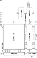
図1は、本発明が適用される固体撮像素子としてのCMOSイメージセンサの構成例を示すブロック図である。
次に、画素アレイ部111に行列状に配置されている単位画素120Aの具体的な構造について説明する。単位画素120Aは、浮遊拡散領域(容量)とは別に、光電変換素子から転送される光電荷を保持する電荷保持領域(以下、「メモリ部」と記述する)を有している。
ここで、電荷保持領域としてのメモリ部123のゲート電極、即ち、第1転送ゲート122のゲート電極122Aの電位について説明する。
より具体的には、第1転送ゲート122若しくは第2転送ゲート124のいずれか一方、または両方を非導通状態とする際に、ゲート電極122A,124Aに印加する電圧が、ゲート電極直下のSi表面に光電荷とは逆の極性のキャリアを蓄積できるピニング状態となるように設定される。
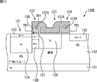
次に、図3および図4を参照して、第1の実施の形態における単位画素120Aの構成について説明する。なお、図3および図4、並びに以下の図面では、図2の単位画素と共通する構成要素には同一の符号を付し、その詳細な説明は省略する。
次に、図5を参照して、単位画素120Aの製造方法について説明する。
次に、図6は、第2の実施の形態における単位画素120Bの断面図である。
次に、図9は、第3の実施の形態における単位画素120Cの断面図である。
次に、図10は、第4の実施の形態における単位画素120Dの断面図である。
次に、図11は、第5の実施の形態における単位画素120Eの断面図である。
次に、図12は、第6の実施の形態における単位画素120Fの断面図である。
次に、図13を参照して、単位画素120Fの製造方法について説明する。
次に、図14および図15を参照して、第7の実施の形態における単位画素120Gについて説明する。図14には、単位画素120Gの平面図が示されており、図15Aには、図14の平面図に示されている矢印A−A’に沿った断面図およびポテンシャル状態が示されており、図15Bには、図14の平面図に示されている矢印B−B’に沿った断面図およびポテンシャル状態が示されている。
図16は、単位画素120のその他の第1構成例である単位画素120H−1の構造を示す図である。
図17は、単位画素120のその他の第2構成例である単位画素120H−2の構造を示す図である。
図18は、単位画素120のその他の第3構成例である単位画素120H−3の構造を示す図である。
さらに本発明は、固体撮像素子への適用に限られるものではない。即ち、本発明は、デジタルスチルカメラやビデオカメラ等の撮像装置や、撮像機能を有する携帯端末装置や、画像読取部に固体撮像素子を用いる複写機など、画像取込部(光電変換部)に固体撮像素子を用いる電子機器全般に対して適用可能である。固体撮像素子は、ワンチップとして形成された形態であってもよいし、撮像部と信号処理部または光学系とがまとめてパッケージングされた撮像機能を有するモジュール状の形態であってもよい。
Claims (12)
- 半導体基板の表面側に形成される第2の導電型による半導体領域と、
第1の導電型の不純物領域からなり、入射光量に応じた電荷を発生して内部に蓄積する光電変換素子と、
前記第1の導電型の不純物領域からなり、前記光電変換素子によって変換された電荷を読み出されるまで保持する電荷保持領域と、
前記光電変換素子と前記電荷保持領域との間の領域に配置される第1の導電型の不純物領域からなり、露光期間中において前記光電変換素子で発生した所定電荷量を超える電荷だけを前記電荷保持領域に転送する中間転送経路と、
前記光電変換素子と前記電荷保持領域との間の領域であって、かつ、前記中間転送経路の下部の領域に配置され、前記第2の導電型による半導体領域よりも不純物濃度が高い第2の導電型の不純物領域からなる不純物層と
を備える固体撮像素子。 - 前記中間転送経路を形成する第1の導電型の前記不純物領域の接合深さは、前記電荷保持領域を形成する第1の導電型の前記不純物領域の接合深さよりも浅く、かつ、前記中間転送経路を形成する第1の導電型の前記不純物領域の不純物濃度は、前記電荷保持領域を形成する第1の導電型の前記不純物領域の不純物濃度よりも低く設定されている
請求項1に記載の固体撮像素子。 - 前記第2の導電型の不純物領域からなる前記不純物層は、前記光電変換素子および前記電荷保持領域のポテンシャルによって空乏状態とならない所定の不純物濃度で形成される
請求項1に記載の固体撮像素子。 - 前記中間転送経路を通過する深さ方向に沿ったポテンシャル状態は、前記電荷保持領域を形成する第1の導電型の前記不純物領域の下端よりも浅い位置に、ポテンシャル極小点およびポテンシャル極大点が少なくとも1つ以上形成され、かつ、前記ポテンシャル極大点が、前記ポテンシャル極小点よりも深い位置に形成される
請求項1に記載の固体撮像素子。 - 前記第2の導電型の不純物領域からなる前記不純物層は、前記電荷保持領域を形成する第1の導電型の前記不純物領域の下端の深さまで形成される
請求項1に記載の固体撮像素子。 - 前記第2の導電型の不純物領域からなる前記不純物層は、前記中間転送経路を形成する第1の導電型の前記不純物領域の直下から、前記電荷保持領域を形成する第1の導電型の前記不純物領域の下部に向かって延在するような形状で形成される
請求項1に記載の固体撮像素子。 - 前記光電変換素子を形成する第1の導電型の前記不純物領域は、その不純物領域の表面に形成された不純物層の直下から、前記電荷保持領域を形成する第1の導電型の前記不純物領域の下部に向かって延在する前記第2の導電型の不純物領域からなる前記不純物層の下部に向かって延在するような形状で形成される
請求項6に記載の固体撮像素子。 - 前記中間転送経路および前記電荷保持領域の上部に設けられ、前記光電変換領域から前記電荷保持領域に電荷を転送する転送ゲートをさらに備え、
前記光電変換素子を形成する第1の導電型の前記不純物領域が形成された領域と、前記転送ゲートとが、平面的に見て互いに重なり合うように配置される
請求項1に記載の固体撮像素子。 - 前記光電変換素子および前記電荷保持領域は、HAD(Hole Accumulated Diode)構造により構成される
請求項1に記載の固体撮像素子。 - 前記中間転送経路の上部を覆う第1の電極と、
前記電荷保持領域の上部を覆う第2の電極と
をさらに備え、
前記第1の電極と前記第2の電極とが分離して形成されている
請求項1に記載の固体撮像素子。 - 第1の導電型の不純物領域からなり、入射光量に応じた電荷を発生して内部に蓄積する光電変換素子を形成し、
前記第1の導電型の不純物領域からなり、前記光電変換素子によって変換された電荷を読み出されるまで保持する電荷保持領域を形成し、
前記光電変換素子と前記電荷保持領域との間の領域に配置される第1の導電型の不純物領域からなり、露光期間中において前記光電変換素子で発生した所定電荷量を超える電荷だけを前記電荷保持領域に転送する中間転送経路を形成し、
前記光電変換素子と前記電荷保持領域との間の領域であって、かつ、前記中間転送経路の下部の領域に配置され、半導体基板の表面側に形成される前記第2の導電型による半導体領域よりも不純物濃度が高い第2の導電型の不純物領域からなる不純物層を形成する
ステップを含む固体撮像素子の製造方法。 - 半導体基板の表面側に形成される第2の導電型による半導体領域と、
第1の導電型の不純物領域からなり、入射光量に応じた電荷を発生して内部に蓄積する光電変換素子と、
前記第1の導電型の不純物領域からなり、前記光電変換素子によって変換された電荷を読み出されるまで保持する電荷保持領域と、
前記光電変換素子と前記電荷保持領域との間の領域に配置される第1の導電型の不純物領域からなり、露光期間中において前記光電変換素子で発生した所定電荷量を超える電荷だけを前記電荷保持領域に転送する中間転送経路と、
前記光電変換素子と前記電荷保持領域との間の領域であって、かつ、前記中間転送経路の下部の領域に配置され、前記第2の導電型による半導体領域よりも不純物濃度が高い第2の導電型の不純物領域からなる不純物層と
を備える固体撮像素子を有し、
行列状に配置された複数行の単位画素が同時に前記電荷の蓄積を行い、
前記光電変換素子から前記電荷保持領域に転送された前記電荷を順次読み出す
電子機器。
Priority Applications (3)
| Application Number | Priority Date | Filing Date | Title |
|---|---|---|---|
| JP2010083600A JP2011216673A (ja) | 2010-03-31 | 2010-03-31 | 固体撮像装置、固体撮像装置の製造方法、および電子機器 |
| US13/053,455 US8629484B2 (en) | 2010-03-31 | 2011-03-22 | Solid-state imaging device, method of manufacturing solid-state imaging device, and electronic apparatus |
| CN201110075913.6A CN102208423B (zh) | 2010-03-31 | 2011-03-24 | 固体摄像装置、制造固体摄像装置的方法和电子设备 |
Applications Claiming Priority (1)
| Application Number | Priority Date | Filing Date | Title |
|---|---|---|---|
| JP2010083600A JP2011216673A (ja) | 2010-03-31 | 2010-03-31 | 固体撮像装置、固体撮像装置の製造方法、および電子機器 |
Publications (2)
| Publication Number | Publication Date |
|---|---|
| JP2011216673A true JP2011216673A (ja) | 2011-10-27 |
| JP2011216673A5 JP2011216673A5 (ja) | 2013-05-09 |
Family
ID=44697173
Family Applications (1)
| Application Number | Title | Priority Date | Filing Date |
|---|---|---|---|
| JP2010083600A Ceased JP2011216673A (ja) | 2010-03-31 | 2010-03-31 | 固体撮像装置、固体撮像装置の製造方法、および電子機器 |
Country Status (3)
| Country | Link |
|---|---|
| US (1) | US8629484B2 (ja) |
| JP (1) | JP2011216673A (ja) |
| CN (1) | CN102208423B (ja) |
Cited By (12)
| Publication number | Priority date | Publication date | Assignee | Title |
|---|---|---|---|---|
| JP2011249406A (ja) * | 2010-05-24 | 2011-12-08 | Brookman Technology Inc | 固体撮像装置 |
| JP2015026696A (ja) * | 2013-07-25 | 2015-02-05 | キヤノン株式会社 | 光電変換装置及び撮像システム |
| JP2015065271A (ja) * | 2013-09-25 | 2015-04-09 | ソニー株式会社 | 固体撮像素子およびその動作方法、並びに電子機器およびその動作方法 |
| JP2015220279A (ja) * | 2014-05-15 | 2015-12-07 | キヤノン株式会社 | 撮像装置 |
| JP2016516294A (ja) * | 2013-03-06 | 2016-06-02 | アップル インコーポレイテッド | 画像センサにおける電荷転送 |
| JP2016111224A (ja) * | 2014-12-08 | 2016-06-20 | 株式会社ブルックマンテクノロジ | 光検出素子及び固体撮像装置 |
| WO2016152184A1 (ja) * | 2015-03-25 | 2016-09-29 | ソニー株式会社 | 固体撮像装置および固体撮像装置の駆動方法 |
| JP2018120981A (ja) * | 2017-01-26 | 2018-08-02 | キヤノン株式会社 | 固体撮像装置、撮像システム、および固体撮像装置の製造方法 |
| JP2019009155A (ja) * | 2017-06-20 | 2019-01-17 | キヤノン株式会社 | 撮像装置、撮像システム、移動体、および、撮像装置の製造方法 |
| JP2019117949A (ja) * | 2019-04-08 | 2019-07-18 | 浜松ホトニクス株式会社 | 固体撮像装置 |
| KR20190086660A (ko) * | 2016-12-01 | 2019-07-23 | 소니 세미컨덕터 솔루션즈 가부시키가이샤 | 고체 촬상 소자, 고체 촬상 소자의 제조 방법 및 촬상 장치 |
| WO2020050007A1 (ja) * | 2018-09-07 | 2020-03-12 | ソニーセミコンダクタソリューションズ株式会社 | 固体撮像装置および電子機器 |
Families Citing this family (42)
| Publication number | Priority date | Publication date | Assignee | Title |
|---|---|---|---|---|
| JP5671830B2 (ja) * | 2010-03-31 | 2015-02-18 | ソニー株式会社 | 固体撮像素子、固体撮像素子の製造方法、および電子機器 |
| JP5637384B2 (ja) * | 2010-12-15 | 2014-12-10 | ソニー株式会社 | 固体撮像素子および駆動方法、並びに電子機器 |
| JP6004665B2 (ja) * | 2012-02-17 | 2016-10-12 | キヤノン株式会社 | 撮像装置、および撮像システム。 |
| JP6012197B2 (ja) * | 2012-02-17 | 2016-10-25 | キヤノン株式会社 | 撮像装置及び撮像装置の駆動方法 |
| KR20130106978A (ko) * | 2012-03-21 | 2013-10-01 | 삼성전자주식회사 | 이미지 센서의 단위 픽셀 및 이를 포함하는 이미지 센서 |
| JP2014011253A (ja) * | 2012-06-28 | 2014-01-20 | Sony Corp | 固体撮像装置および電子機器 |
| US9293500B2 (en) | 2013-03-01 | 2016-03-22 | Apple Inc. | Exposure control for image sensors |
| US9276031B2 (en) | 2013-03-04 | 2016-03-01 | Apple Inc. | Photodiode with different electric potential regions for image sensors |
| US9041837B2 (en) * | 2013-03-05 | 2015-05-26 | Apple Inc. | Image sensor with reduced blooming |
| US9549099B2 (en) | 2013-03-12 | 2017-01-17 | Apple Inc. | Hybrid image sensor |
| US9319611B2 (en) | 2013-03-14 | 2016-04-19 | Apple Inc. | Image sensor with flexible pixel summing |
| JP2015095468A (ja) * | 2013-11-08 | 2015-05-18 | ソニー株式会社 | 固体撮像素子および固体撮像素子の製造方法、並びに電子機器 |
| US9596423B1 (en) | 2013-11-21 | 2017-03-14 | Apple Inc. | Charge summing in an image sensor |
| US9596420B2 (en) | 2013-12-05 | 2017-03-14 | Apple Inc. | Image sensor having pixels with different integration periods |
| US9473706B2 (en) | 2013-12-09 | 2016-10-18 | Apple Inc. | Image sensor flicker detection |
| US10285626B1 (en) | 2014-02-14 | 2019-05-14 | Apple Inc. | Activity identification using an optical heart rate monitor |
| US9232150B2 (en) | 2014-03-12 | 2016-01-05 | Apple Inc. | System and method for estimating an ambient light condition using an image sensor |
| US9277144B2 (en) | 2014-03-12 | 2016-03-01 | Apple Inc. | System and method for estimating an ambient light condition using an image sensor and field-of-view compensation |
| US9584743B1 (en) | 2014-03-13 | 2017-02-28 | Apple Inc. | Image sensor with auto-focus and pixel cross-talk compensation |
| US9497397B1 (en) | 2014-04-08 | 2016-11-15 | Apple Inc. | Image sensor with auto-focus and color ratio cross-talk comparison |
| US9538106B2 (en) | 2014-04-25 | 2017-01-03 | Apple Inc. | Image sensor having a uniform digital power signature |
| US9686485B2 (en) | 2014-05-30 | 2017-06-20 | Apple Inc. | Pixel binning in an image sensor |
| JP2017054947A (ja) * | 2015-09-10 | 2017-03-16 | セイコーエプソン株式会社 | 固体撮像素子及びその製造方法、並びに、電子機器 |
| JP2017143189A (ja) * | 2016-02-10 | 2017-08-17 | ルネサスエレクトロニクス株式会社 | 固体撮像素子 |
| US9912883B1 (en) | 2016-05-10 | 2018-03-06 | Apple Inc. | Image sensor with calibrated column analog-to-digital converters |
| EP3516692B1 (en) | 2016-09-23 | 2022-02-16 | Apple Inc. | Stacked backside illuminated spad array |
| WO2018140522A2 (en) | 2017-01-25 | 2018-08-02 | Apple Inc. | Spad detector having modulated sensitivity |
| US10656251B1 (en) | 2017-01-25 | 2020-05-19 | Apple Inc. | Signal acquisition in a SPAD detector |
| US10962628B1 (en) | 2017-01-26 | 2021-03-30 | Apple Inc. | Spatial temporal weighting in a SPAD detector |
| WO2018193747A1 (en) * | 2017-04-19 | 2018-10-25 | Sony Semiconductor Solutions Corporation | Semiconductor device, method of manufacturing the same, and electronic apparatus |
| US10622538B2 (en) | 2017-07-18 | 2020-04-14 | Apple Inc. | Techniques for providing a haptic output and sensing a haptic input using a piezoelectric body |
| US10440301B2 (en) | 2017-09-08 | 2019-10-08 | Apple Inc. | Image capture device, pixel, and method providing improved phase detection auto-focus performance |
| CN110098203A (zh) * | 2018-01-30 | 2019-08-06 | 维深半导体公司 | 背照式图像传感器及其制备 |
| US10559614B2 (en) * | 2018-03-09 | 2020-02-11 | Semiconductor Components Industries, Llc | Dual conversion gain circuitry with buried channels |
| US11019294B2 (en) | 2018-07-18 | 2021-05-25 | Apple Inc. | Seamless readout mode transitions in image sensors |
| US10848693B2 (en) | 2018-07-18 | 2020-11-24 | Apple Inc. | Image flare detection using asymmetric pixels |
| US11233966B1 (en) | 2018-11-29 | 2022-01-25 | Apple Inc. | Breakdown voltage monitoring for avalanche diodes |
| TWI685959B (zh) * | 2019-01-07 | 2020-02-21 | 力晶積成電子製造股份有限公司 | 影像感測器及其製造方法 |
| US11503234B2 (en) * | 2019-02-27 | 2022-11-15 | Canon Kabushiki Kaisha | Photoelectric conversion device, imaging system, radioactive ray imaging system, and movable object |
| KR20210133739A (ko) * | 2020-04-29 | 2021-11-08 | 에스케이하이닉스 주식회사 | 이미지 센서 |
| US11563910B2 (en) | 2020-08-04 | 2023-01-24 | Apple Inc. | Image capture devices having phase detection auto-focus pixels |
| US11546532B1 (en) | 2021-03-16 | 2023-01-03 | Apple Inc. | Dynamic correlated double sampling for noise rejection in image sensors |
Citations (6)
| Publication number | Priority date | Publication date | Assignee | Title |
|---|---|---|---|---|
| JP2005347758A (ja) * | 2004-06-04 | 2005-12-15 | Samsung Electronics Co Ltd | Cmosイメージセンサー及びその製造方法 |
| JP2008004692A (ja) * | 2006-06-21 | 2008-01-10 | Nikon Corp | 固体撮像装置 |
| JP2008103647A (ja) * | 2006-10-20 | 2008-05-01 | National Univ Corp Shizuoka Univ | 半導体素子及び固体撮像装置 |
| JP2009253150A (ja) * | 2008-04-09 | 2009-10-29 | Canon Inc | 固体撮像装置 |
| JP2009253149A (ja) * | 2008-04-09 | 2009-10-29 | Canon Inc | 光電変換装置及びそれを用いた撮像システム |
| JP2009268083A (ja) * | 2008-04-03 | 2009-11-12 | Sony Corp | 固体撮像装置、固体撮像装置の駆動方法および電子機器 |
Family Cites Families (2)
| Publication number | Priority date | Publication date | Assignee | Title |
|---|---|---|---|---|
| KR100761824B1 (ko) * | 2004-06-04 | 2007-09-28 | 삼성전자주식회사 | 이미지 센서 및 그 제조 방법 |
| JP5671830B2 (ja) * | 2010-03-31 | 2015-02-18 | ソニー株式会社 | 固体撮像素子、固体撮像素子の製造方法、および電子機器 |
-
2010
- 2010-03-31 JP JP2010083600A patent/JP2011216673A/ja not_active Ceased
-
2011
- 2011-03-22 US US13/053,455 patent/US8629484B2/en not_active Expired - Fee Related
- 2011-03-24 CN CN201110075913.6A patent/CN102208423B/zh not_active Expired - Fee Related
Patent Citations (6)
| Publication number | Priority date | Publication date | Assignee | Title |
|---|---|---|---|---|
| JP2005347758A (ja) * | 2004-06-04 | 2005-12-15 | Samsung Electronics Co Ltd | Cmosイメージセンサー及びその製造方法 |
| JP2008004692A (ja) * | 2006-06-21 | 2008-01-10 | Nikon Corp | 固体撮像装置 |
| JP2008103647A (ja) * | 2006-10-20 | 2008-05-01 | National Univ Corp Shizuoka Univ | 半導体素子及び固体撮像装置 |
| JP2009268083A (ja) * | 2008-04-03 | 2009-11-12 | Sony Corp | 固体撮像装置、固体撮像装置の駆動方法および電子機器 |
| JP2009253150A (ja) * | 2008-04-09 | 2009-10-29 | Canon Inc | 固体撮像装置 |
| JP2009253149A (ja) * | 2008-04-09 | 2009-10-29 | Canon Inc | 光電変換装置及びそれを用いた撮像システム |
Cited By (22)
| Publication number | Priority date | Publication date | Assignee | Title |
|---|---|---|---|---|
| JP2011249406A (ja) * | 2010-05-24 | 2011-12-08 | Brookman Technology Inc | 固体撮像装置 |
| JP2016516294A (ja) * | 2013-03-06 | 2016-06-02 | アップル インコーポレイテッド | 画像センサにおける電荷転送 |
| JP2015026696A (ja) * | 2013-07-25 | 2015-02-05 | キヤノン株式会社 | 光電変換装置及び撮像システム |
| US11070760B2 (en) | 2013-09-25 | 2021-07-20 | Sony Semiconductor Solutions Corporation | Solid-state imaging device and method of operating the same, and electronic apparatus and method of operating the same |
| JP2015065271A (ja) * | 2013-09-25 | 2015-04-09 | ソニー株式会社 | 固体撮像素子およびその動作方法、並びに電子機器およびその動作方法 |
| US9571776B2 (en) | 2013-09-25 | 2017-02-14 | Sony Semiconductor Solutions Corporation | Solid-state imaging device and method of operating the same, and electronic apparatus and method of operating the same |
| US9832410B2 (en) | 2013-09-25 | 2017-11-28 | Sony Semiconductor Solutions Corporation | Solid-state imaging device and electronic apparatus including plurality of charge holding electrodes, and method of operating the same |
| US10574924B2 (en) | 2013-09-25 | 2020-02-25 | Sony Semiconductor Solutions Corporation | Solid-state imaging device and method of operating the same, and electronic apparatus and method of operating the same |
| US11627275B2 (en) | 2013-09-25 | 2023-04-11 | Sony Semiconductor Solutions Corporation | Solid-state imaging device and method of operating the same, and electronic apparatus and method of operating the same |
| US10104327B2 (en) | 2013-09-25 | 2018-10-16 | Sony Semiconductor Solutions Corporation | Solid-State imaging device and electronic apparatus including plurality of charge holding electrodes and method of operating the same |
| JP2015220279A (ja) * | 2014-05-15 | 2015-12-07 | キヤノン株式会社 | 撮像装置 |
| JP2016111224A (ja) * | 2014-12-08 | 2016-06-20 | 株式会社ブルックマンテクノロジ | 光検出素子及び固体撮像装置 |
| WO2016152184A1 (ja) * | 2015-03-25 | 2016-09-29 | ソニー株式会社 | 固体撮像装置および固体撮像装置の駆動方法 |
| US10205893B2 (en) | 2015-03-25 | 2019-02-12 | Sony Corporation | Solid-state imaging device and driving method of solid-state imaging device |
| JPWO2016152184A1 (ja) * | 2015-03-25 | 2018-01-18 | ソニー株式会社 | 固体撮像装置および固体撮像装置の駆動方法 |
| KR20190086660A (ko) * | 2016-12-01 | 2019-07-23 | 소니 세미컨덕터 솔루션즈 가부시키가이샤 | 고체 촬상 소자, 고체 촬상 소자의 제조 방법 및 촬상 장치 |
| KR102476411B1 (ko) * | 2016-12-01 | 2022-12-12 | 소니 세미컨덕터 솔루션즈 가부시키가이샤 | 고체 촬상 소자, 고체 촬상 소자의 제조 방법 및 촬상 장치 |
| JP2018120981A (ja) * | 2017-01-26 | 2018-08-02 | キヤノン株式会社 | 固体撮像装置、撮像システム、および固体撮像装置の製造方法 |
| JP2019009155A (ja) * | 2017-06-20 | 2019-01-17 | キヤノン株式会社 | 撮像装置、撮像システム、移動体、および、撮像装置の製造方法 |
| WO2020050007A1 (ja) * | 2018-09-07 | 2020-03-12 | ソニーセミコンダクタソリューションズ株式会社 | 固体撮像装置および電子機器 |
| US11438534B2 (en) | 2018-09-07 | 2022-09-06 | Sony Semiconductor Solutions Corporation | Solid-state imaging device and electronic apparatus |
| JP2019117949A (ja) * | 2019-04-08 | 2019-07-18 | 浜松ホトニクス株式会社 | 固体撮像装置 |
Also Published As
| Publication number | Publication date |
|---|---|
| CN102208423B (zh) | 2015-08-19 |
| CN102208423A (zh) | 2011-10-05 |
| US8629484B2 (en) | 2014-01-14 |
| US20110241089A1 (en) | 2011-10-06 |
Similar Documents
| Publication | Publication Date | Title |
|---|---|---|
| JP2011216673A (ja) | 固体撮像装置、固体撮像装置の製造方法、および電子機器 | |
| JP5671830B2 (ja) | 固体撮像素子、固体撮像素子の製造方法、および電子機器 | |
| US10229941B2 (en) | Solid-state imaging element, driving method, and electronic apparatus | |
| US8810703B2 (en) | Solid-state image pickup device, driving method of solid-state image pickup device, and electronic device | |
| JP5651976B2 (ja) | 固体撮像素子およびその製造方法、並びに電子機器 | |
| US8716719B2 (en) | Solid-state imaging device, method of manufacturing solid-state imaging device, and electronic apparatus | |
| JP5282543B2 (ja) | 固体撮像装置、固体撮像装置の駆動方法および撮像装置 | |
| JP4752926B2 (ja) | 固体撮像装置、固体撮像装置の製造方法、固体撮像装置の駆動方法、電子機器 | |
| US20130037900A1 (en) | Solid-state imaging element, manufacturing method, and electronic device | |
| JP2011204878A (ja) | 固体撮像デバイスおよび電子機器 | |
| JP2015023250A (ja) | 固体撮像素子及びその駆動方法、並びに電子機器 | |
| JP2014060519A (ja) | 固体撮像素子及びその制御方法、並びに電子機器 | |
| JP5407761B2 (ja) | 固体撮像装置、電子機器 | |
| JP2013145779A (ja) | 固体撮像装置及び電子機器 | |
| US20110241080A1 (en) | Solid-state imaging device, method for manufacturing the same, and electronic apparatus | |
| JP2013254805A (ja) | 固体撮像素子及びその制御方法、並びに電子機器 | |
| JP2010114275A (ja) | 固体撮像装置、固体撮像装置の駆動方法、及び電子機器 | |
| US9406816B2 (en) | Solid-state imaging apparatus, method of manufacturing solid-state imaging apparatus and electronic device | |
| JP2013033885A (ja) | 固体撮像装置とその製造方法及び駆動方法、並びに電子機器 | |
| JP2022017616A (ja) | 固体撮像装置、固体撮像装置の製造方法および電子機器 | |
| JP2011216961A (ja) | 固体撮像装置、固体撮像装置の駆動方法、および、電子機器 | |
| JP2011204991A (ja) | 固体撮像素子およびその製造方法、並びに電子機器 | |
| JP2021103793A (ja) | 受光素子及び電子機器 | |
| JP2006165006A (ja) | 固体撮像素子 | |
| JP2011003737A (ja) | 固体撮像素子、撮像装置 |
Legal Events
| Date | Code | Title | Description |
|---|---|---|---|
| A521 | Request for written amendment filed |
Free format text: JAPANESE INTERMEDIATE CODE: A523 Effective date: 20130322 |
|
| A621 | Written request for application examination |
Free format text: JAPANESE INTERMEDIATE CODE: A621 Effective date: 20130322 |
|
| A977 | Report on retrieval |
Free format text: JAPANESE INTERMEDIATE CODE: A971007 Effective date: 20140205 |
|
| A131 | Notification of reasons for refusal |
Free format text: JAPANESE INTERMEDIATE CODE: A131 Effective date: 20140213 |
|
| A521 | Request for written amendment filed |
Free format text: JAPANESE INTERMEDIATE CODE: A523 Effective date: 20140411 |
|
| A131 | Notification of reasons for refusal |
Free format text: JAPANESE INTERMEDIATE CODE: A131 Effective date: 20141113 |
|
| A521 | Request for written amendment filed |
Free format text: JAPANESE INTERMEDIATE CODE: A523 Effective date: 20150107 |
|
| A01 | Written decision to grant a patent or to grant a registration (utility model) |
Free format text: JAPANESE INTERMEDIATE CODE: A01 Effective date: 20150127 |
|
| A045 | Written measure of dismissal of application [lapsed due to lack of payment] |
Free format text: JAPANESE INTERMEDIATE CODE: A045 Effective date: 20150526 |