JP5329068B2 - 半導体装置 - Google Patents
半導体装置 Download PDFInfo
- Publication number
- JP5329068B2 JP5329068B2 JP2007274216A JP2007274216A JP5329068B2 JP 5329068 B2 JP5329068 B2 JP 5329068B2 JP 2007274216 A JP2007274216 A JP 2007274216A JP 2007274216 A JP2007274216 A JP 2007274216A JP 5329068 B2 JP5329068 B2 JP 5329068B2
- Authority
- JP
- Japan
- Prior art keywords
- protective
- wiring layer
- semiconductor device
- insulating film
- interlayer insulating
- Prior art date
- Legal status (The legal status is an assumption and is not a legal conclusion. Google has not performed a legal analysis and makes no representation as to the accuracy of the status listed.)
- Expired - Fee Related
Links
Images


Classifications
-
- H—ELECTRICITY
- H10—SEMICONDUCTOR DEVICES; ELECTRIC SOLID-STATE DEVICES NOT OTHERWISE PROVIDED FOR
- H10W—GENERIC PACKAGES, INTERCONNECTIONS, CONNECTORS OR OTHER CONSTRUCTIONAL DETAILS OF DEVICES COVERED BY CLASS H10
- H10W20/00—Interconnections in chips, wafers or substrates
- H10W20/40—Interconnections external to wafers or substrates, e.g. back-end-of-line [BEOL] metallisations or vias connecting to gate electrodes
- H10W20/41—Interconnections external to wafers or substrates, e.g. back-end-of-line [BEOL] metallisations or vias connecting to gate electrodes characterised by their conductive parts
- H10W20/42—Vias, e.g. via plugs
-
- H—ELECTRICITY
- H10—SEMICONDUCTOR DEVICES; ELECTRIC SOLID-STATE DEVICES NOT OTHERWISE PROVIDED FOR
- H10W—GENERIC PACKAGES, INTERCONNECTIONS, CONNECTORS OR OTHER CONSTRUCTIONAL DETAILS OF DEVICES COVERED BY CLASS H10
- H10W72/00—Interconnections or connectors in packages
- H10W72/01—Manufacture or treatment
- H10W72/019—Manufacture or treatment of bond pads
-
- H—ELECTRICITY
- H10—SEMICONDUCTOR DEVICES; ELECTRIC SOLID-STATE DEVICES NOT OTHERWISE PROVIDED FOR
- H10W—GENERIC PACKAGES, INTERCONNECTIONS, CONNECTORS OR OTHER CONSTRUCTIONAL DETAILS OF DEVICES COVERED BY CLASS H10
- H10W72/00—Interconnections or connectors in packages
- H10W72/90—Bond pads, in general
- H10W72/921—Structures or relative sizes of bond pads
- H10W72/923—Bond pads having multiple stacked layers
- H10W72/9232—Bond pads having multiple stacked layers with additional elements interposed between layers
-
- H—ELECTRICITY
- H10—SEMICONDUCTOR DEVICES; ELECTRIC SOLID-STATE DEVICES NOT OTHERWISE PROVIDED FOR
- H10W—GENERIC PACKAGES, INTERCONNECTIONS, CONNECTORS OR OTHER CONSTRUCTIONAL DETAILS OF DEVICES COVERED BY CLASS H10
- H10W72/00—Interconnections or connectors in packages
- H10W72/90—Bond pads, in general
- H10W72/921—Structures or relative sizes of bond pads
- H10W72/926—Multiple bond pads having different sizes
-
- H—ELECTRICITY
- H10—SEMICONDUCTOR DEVICES; ELECTRIC SOLID-STATE DEVICES NOT OTHERWISE PROVIDED FOR
- H10W—GENERIC PACKAGES, INTERCONNECTIONS, CONNECTORS OR OTHER CONSTRUCTIONAL DETAILS OF DEVICES COVERED BY CLASS H10
- H10W72/00—Interconnections or connectors in packages
- H10W72/90—Bond pads, in general
- H10W72/931—Shapes of bond pads
- H10W72/932—Plan-view shape, i.e. in top view
-
- H—ELECTRICITY
- H10—SEMICONDUCTOR DEVICES; ELECTRIC SOLID-STATE DEVICES NOT OTHERWISE PROVIDED FOR
- H10W—GENERIC PACKAGES, INTERCONNECTIONS, CONNECTORS OR OTHER CONSTRUCTIONAL DETAILS OF DEVICES COVERED BY CLASS H10
- H10W72/00—Interconnections or connectors in packages
- H10W72/90—Bond pads, in general
- H10W72/951—Materials of bond pads
- H10W72/952—Materials of bond pads comprising metals or metalloids, e.g. PbSn, Ag or Cu
-
- H—ELECTRICITY
- H10—SEMICONDUCTOR DEVICES; ELECTRIC SOLID-STATE DEVICES NOT OTHERWISE PROVIDED FOR
- H10W—GENERIC PACKAGES, INTERCONNECTIONS, CONNECTORS OR OTHER CONSTRUCTIONAL DETAILS OF DEVICES COVERED BY CLASS H10
- H10W72/00—Interconnections or connectors in packages
- H10W72/90—Bond pads, in general
- H10W72/981—Auxiliary members, e.g. spacers
- H10W72/983—Reinforcing structures, e.g. collars
Landscapes
- Internal Circuitry In Semiconductor Integrated Circuit Devices (AREA)
- Wire Bonding (AREA)
- Testing Or Measuring Of Semiconductors Or The Like (AREA)
Description
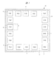
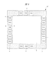
図1は本実施の形態における半導体装置(半導体チップ1C)の平面を示す模式図である。半導体チップ1Cを構成する半導体基板1Sの表面には、表面保護膜(パッシベーション膜)によって覆われた素子形成領域2と、その外周の外周領域3とが設けられている。素子形成領域2ではMISFETなどが形成されており、それらと電気的に接続された電極パッド(PAD)4が外部端子として設けられている。また外周領域3では半導体ウエハから半導体チップ1Cを切り出す際のマージン領域を含めて、外部から素子形成領域2内への水分侵入を防止する手段が施されている。
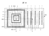
前記実施の形態1では、例えば図3に示したように、平面リングの形状が矩形状の保護用Via9の場合について説明した。これに対して本実施の形態では、保護用Via9の平面リングの形状を種々変形した場合について説明する。図20〜図22は本実施の形態における半導体装置の要部の平面を示す模式図である。本実施の形態における保護用Via9は、例えば図5を参照して説明したように、電極パッド4にプローブピン14が接触したときに発生したストレス16によって、平面リング状の保護用Via9および保護用配線層10の外側にクラック15を進行させないようにしたものである。以下に、保護用Via9の形状以外の構成は前記実施の形態1と同様であるので、相違する点を中心に説明する。なお、本実施の形態における半導体装置は、前記実施の形態1で説明した製造方法と同様の工程で製造することができる。
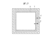
前記実施の形態1では、例えば図3に示したように、平面リングの形状が矩形状の保護用Via9を1つ用いた場合について説明した。これに対して本実施の形態では、保護用Via9のリング内側に別のVia(以下、内側Viaという)を設ける場合について説明する。図23は、本実施の形態における半導体装置の要部の平面を示す模式図である。本実施の形態における保護用Via9および内側Via21は、例えば図5に示したように、平面リング状の保護用Via9上の電極パッド4にプローブピン14が接触したときに発生したストレス16によって、リング外側にクラック15を進行させないようにしたものである。以下に、内側Via21を設ける以外の構成は前記実施の形態1と同様であるので、相違する点を中心に説明する。なお、内側Via21は、保護用Via9と同様に形成される。また、本実施の形態における半導体装置は、前記実施の形態1で説明した製造方法と同様の工程で製造することができる。
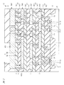
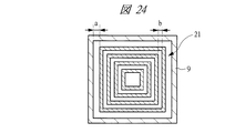
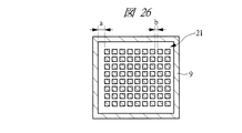
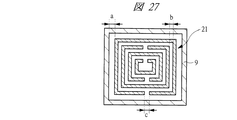
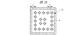
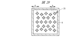
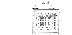
本実施の形態では、前記実施の形態1で示した平面リング状の保護用Via9(例えば図3参照)のリング内側にVia(以下、内側Viaという)を設ける場合について説明する。図24〜図31は、本実施の形態における半導体装置の要部の平面を示す模式図である。本実施の形態における保護用Via9および内側Via21は、例えば図5に示したように、平面リング状の保護用Via9上の電極パッド4にプローブピン14が接触したときに発生したストレス16によって、保護用Via9の外側にクラック15を進行させないようにしたものである。以下に、内側Via21を設ける以外の構成は前記実施の形態1と同様であるので、相違する点を中心に説明する。なお、内側Via21は、保護用Via9と同様に形成される。また、本実施の形態における半導体装置は、前記実施の形態1で説明した製造方法と同様の工程で製造することができる。
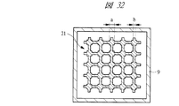
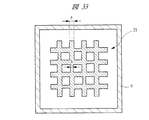
本実施の形態では、前記実施の形態1で示した平面リング状の保護用Via9(例えば図3参照)のリング内側にVia(以下、内側Viaという)を設ける場合について説明する。図32〜図34は、本実施の形態における半導体装置の要部の平面を示す模式図である。本実施の形態における保護用Via9および内側Via21は、例えば図5に示したように、平面リング状の保護用Via9上の電極パッド4にプローブピン14が接触したときに発生したストレス16によって、保護用Via9の外側にクラック15を進行させないようにしたものである。以下に、内側Via21を設ける以外の構成は前記実施の形態1と同様であるので、相違する点を中心に説明する。なお、内側Via21は、保護用Via9と同様に形成される。また、本実施の形態における半導体装置は、前記実施の形態1で説明した製造方法と同様の工程で製造することができる。
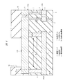
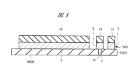
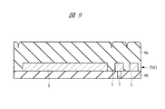
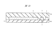
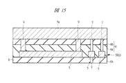
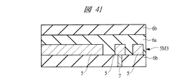
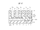
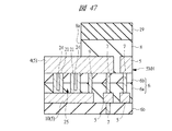
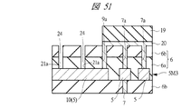
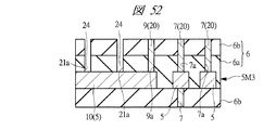
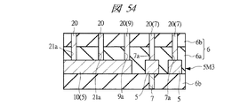
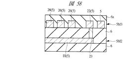
図35は本実施の形態における半導体装置の要部の断面を示す模式図である。前記実施の形態1では、例えば図2に示したように、4層の配線層5のうち最上層である第4層の配線層5M4の一部に電極パッド4、その下の第3層の配線層5M3の一部に保護用配線層10、電極パッド4と保護用配線層10との間に保護用Via9を設けた場合について説明した。これに対して本実施の形態では、図35に示すように、配線層5M3ではなく、その下の第2層の配線層5M2に保護用配線層10を設け、電極パッド4と保護用配線層10との間に2つの保護用Via9、23およびそれらを接続する中間層22を設けている点のみが相違する。
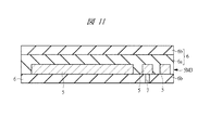
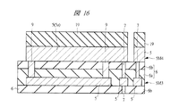
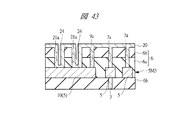
図36は本実施の形態における半導体装置の要部の断面を示す模式図である。前記実施の形態1では、例えば図2に示したように、4層の配線層5のうち最上層である第4層の配線層5M4の一部に電極パッド4、その下の第3層の配線層5M3の一部に保護用配線層10、電極パッド4と保護用配線層10との間に保護用Via9を設けた場合について説明した。これに対して本実施の形態では、図36に示すように、第3層の配線層5M3ではなく、その下の第2層の配線層5M2に保護用配線層10を設け、電極パッド4と保護用配線層10との間に2つの保護用Via9、23を設けている点のみが相違する。
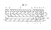
前記実施の形態1は、例えば図5を参照して説明したように、電極パッド4にプローブピン14が接触したときに電極パッド4下の層間絶縁膜6にクラック15が発生することを考慮して、平面リング状の保護用Via9および保護用配線層10の外側にクラック15を進行させないようにしたものである。本実施の形態は、電極パッド下の層間絶縁膜6にクラック15を発生させるのを防止して、保護用Via9および保護用配線層10の外側にクラック15を進行させないようにするものである。以下に、前記実施の形態1と相違する点を中心に説明する。
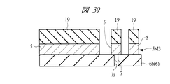
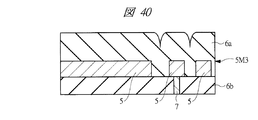
前記実施の形態8は、例えば図38を参照して説明したように、保護用Via9および保護用配線層10で囲まれた層間絶縁膜6に、内側Via21および空隙24を設けたものである。本実施の形態は、電極パッド4下において保護用Via9および保護用配線層10で囲まれた層間絶縁膜6に、空隙24のみを設けるものである。以下に、前記実施の形態8と相違する点を中心に説明する。
前記実施の形態8は、例えば図38を参照して説明したように、保護用Via9および保護用配線層10で囲まれた層間絶縁膜6に、内側Via21および空隙24を設けたものである。本実施の形態は、電極パッド4下において保護用Via9、23、保護用配線層10および中間層22で囲まれた層間絶縁膜6に、空隙24を有する内側配線層26を設けるものである。以下に、前記実施の形態8と相違する点を中心に説明する。
前記実施の形態1〜10では、配線層として、アルニミウムを主成分とする配線を例示したが、本実施の形態では、銅を主成分とする配線を含む場合について説明する。
前記実施の形態1〜11では、電極パッド4の下方の活性領域にMISFET12等の半導体素子や配線層5を形成した場合を例示したが、本実施の形態では図64に示すように、ダミー活性領域DLおよびダミー配線DMを形成した場合を例示している。
1S 半導体基板
2 素子形成領域
3 外周領域
4 電極パッド
4a 接触領域
5、5M1、5M2、5M3、5M4 配線層
5a 金属膜
6、6a、6b、6c 層間絶縁膜
7 回路用Via
7a 孔
8 表面保護膜
8a パッド開口部
9 保護用Via
9a 溝
10 保護用配線層
11 素子分離領域
12 MISFET
12a 絶縁膜
12b 導電性膜
12c 半導体領域
13 コンタクト
14 プローブピン
15 クラック
16 ストレス
17 配線層
18 電極
19 ホトレジスト膜
20 金属膜
21 内側Via
21a 溝
22 中間層
23 保護用Via
24 空隙
25 緩衝領域
26 内側配線層
27 溝
28 バリアメタル膜
29 材料膜
30 孔
DL ダミー活性領域
DM ダミー配線
Claims (9)
- 半導体基板と、
前記半導体基板上に形成された半導体素子と、
前記半導体素子を覆うように形成された層間絶縁膜と、
前記層間絶縁膜中に形成された第1配線層と、
前記第1配線層と接続し、かつ、前記層間絶縁膜中に形成された第1ビアと、
前記第1ビアと接続し、かつ、前記層間絶縁膜上に形成された第2配線層と、
前記第1配線層と同層で、かつ、前記層間絶縁膜中に形成された第3配線層と、
前記第1ビアと同層で、前記第3配線層と接続し、かつ、前記層間絶縁膜中に形成された平面リング状の第2ビアと、
前記第2配線層と同層で、前記第2ビアと接続し、かつ、前記層間絶縁膜上に形成されたパッドと、
前記パッド及び前記第2配線層を覆うように前記層間絶縁膜上に形成され、かつ、パッドの上部に開口部を有する絶縁膜と、を有し、
前記第2ビアの幅は、前記第1ビアの幅よりも大きく、
前記第2ビアの平面リング状は矩形状であって、角部の幅が辺部の幅より大きいことを特徴とする半導体装置。 - 請求項1記載の半導体装置において、
平面リング状の前記第2ビアで囲まれた平面領域は、前記パッドと前記第2ビアと前記第3配線層とで囲まれていることを特徴とする半導体装置。 - 請求項2記載の半導体装置において、
前記第2ビアで囲まれた平面領域は、前記開口部の平面領域より大きいことを特徴とする半導体装置。 - 請求項3記載の半導体装置において、
前記パッドの端から前記第2ビアの内側の端までの距離が0より大きいことを特徴とする半導体装置。 - 請求項3記載の半導体装置において、
前記パッドと前記第2ビアが平面的に重なっていることを特徴とする半導体装置。 - 請求項1記載の半導体装置において、
平面リング状の前記第2ビアの内側には、前記第2ビアより幅が小さい平面リング状の第3ビアが設けられていることを特徴とする半導体装置。 - 請求項1記載の半導体装置において、
平面リング状の前記第2ビアの内側には、前記パッドおよび前記第3配線層に接続する複数の第3ビアが設けられており、
前記第2ビアと前記第3ビアとの距離は、前記複数の第3ビア間の距離より大きいことを特徴とする半導体装置。 - 請求項1記載の半導体装置において、
平面リング状の前記第2ビアの内側には、前記パッドおよび前記第3配線層に接続し、且つ、平面メッシュ状の第3ビアが設けられており、
前記平面メッシュ状の交点以外の前記第3ビアの幅が、前記第1ビアの幅と同じであることを特徴とする半導体装置。 - 請求項1記載の半導体装置において、
平面リング状の前記第2ビアの内側には、前記パッドおよび前記第3配線層に接続し、且つ、平面リング状の多重の第3ビアが設けられており、
前記多重の第3ビアの一部の幅が、前記第1ビアの幅と同じであることを特徴とする半導体装置。
Priority Applications (3)
| Application Number | Priority Date | Filing Date | Title |
|---|---|---|---|
| JP2007274216A JP5329068B2 (ja) | 2007-10-22 | 2007-10-22 | 半導体装置 |
| US12/239,809 US20090102059A1 (en) | 2007-10-22 | 2008-09-28 | Semiconductor device |
| US13/924,175 US20130285057A1 (en) | 2007-10-22 | 2013-06-21 | Semiconductor device |
Applications Claiming Priority (1)
| Application Number | Priority Date | Filing Date | Title |
|---|---|---|---|
| JP2007274216A JP5329068B2 (ja) | 2007-10-22 | 2007-10-22 | 半導体装置 |
Related Child Applications (1)
| Application Number | Title | Priority Date | Filing Date |
|---|---|---|---|
| JP2013126032A Division JP5553923B2 (ja) | 2013-06-14 | 2013-06-14 | 半導体装置 |
Publications (3)
| Publication Number | Publication Date |
|---|---|
| JP2009105160A JP2009105160A (ja) | 2009-05-14 |
| JP2009105160A5 JP2009105160A5 (ja) | 2013-04-25 |
| JP5329068B2 true JP5329068B2 (ja) | 2013-10-30 |
Family
ID=40562659
Family Applications (1)
| Application Number | Title | Priority Date | Filing Date |
|---|---|---|---|
| JP2007274216A Expired - Fee Related JP5329068B2 (ja) | 2007-10-22 | 2007-10-22 | 半導体装置 |
Country Status (2)
| Country | Link |
|---|---|
| US (2) | US20090102059A1 (ja) |
| JP (1) | JP5329068B2 (ja) |
Families Citing this family (35)
| Publication number | Priority date | Publication date | Assignee | Title |
|---|---|---|---|---|
| JP5705857B2 (ja) * | 2009-09-16 | 2015-04-22 | マラディン テクノロジーズ リミテッドMaradin Technologies Ltd. | 微小コイル装置およびその製作方法 |
| JP5610905B2 (ja) * | 2010-08-02 | 2014-10-22 | パナソニック株式会社 | 半導体装置 |
| KR20120069119A (ko) * | 2010-12-20 | 2012-06-28 | 에스케이하이닉스 주식회사 | 반도체 장치 |
| JP5922331B2 (ja) * | 2011-02-02 | 2016-05-24 | ラピスセミコンダクタ株式会社 | 半導体装置の配線構造及びその製造方法 |
| JP5882069B2 (ja) * | 2011-03-29 | 2016-03-09 | エスアイアイ・セミコンダクタ株式会社 | 半導体装置及びその製造方法 |
| JP5837783B2 (ja) * | 2011-09-08 | 2015-12-24 | ルネサスエレクトロニクス株式会社 | 半導体集積回路装置 |
| JP5660466B2 (ja) * | 2011-10-07 | 2015-01-28 | 株式会社デンソー | 半導体装置及び半導体装置の製造方法 |
| US9166054B2 (en) * | 2012-04-13 | 2015-10-20 | Semiconductor Energy Laboratory Co., Ltd. | Semiconductor device and manufacturing method thereof |
| TW201401396A (zh) * | 2012-05-25 | 2014-01-01 | 村田製作所股份有限公司 | 半導體裝置 |
| US20130320522A1 (en) * | 2012-05-30 | 2013-12-05 | Taiwan Semiconductor Manufacturing Company, Ltd. | Re-distribution Layer Via Structure and Method of Making Same |
| JP6008603B2 (ja) * | 2012-06-15 | 2016-10-19 | エスアイアイ・セミコンダクタ株式会社 | 半導体装置 |
| JP6157100B2 (ja) | 2012-12-13 | 2017-07-05 | ルネサスエレクトロニクス株式会社 | 半導体装置 |
| JP6027452B2 (ja) * | 2013-02-01 | 2016-11-16 | エスアイアイ・セミコンダクタ株式会社 | 半導体装置 |
| JP2015002234A (ja) * | 2013-06-14 | 2015-01-05 | サンケン電気株式会社 | 半導体装置及びその製造方法 |
| JP2015032661A (ja) * | 2013-08-01 | 2015-02-16 | ルネサスエレクトロニクス株式会社 | 半導体装置とその製造方法および半導体装置の実装方法 |
| JP6212720B2 (ja) * | 2013-09-20 | 2017-10-18 | パナソニックIpマネジメント株式会社 | 半導体装置及びその製造方法 |
| JP2015103776A (ja) * | 2013-11-28 | 2015-06-04 | 日本電信電話株式会社 | 多層配線用パッド構造 |
| US9711451B2 (en) * | 2014-01-29 | 2017-07-18 | Renesas Electronics Corporation | Semiconductor device with coils in different wiring layers |
| US9230941B2 (en) * | 2014-03-28 | 2016-01-05 | Taiwan Semiconductor Manufacturing Company, Ltd. | Bonding structure for stacked semiconductor devices |
| US10109599B2 (en) * | 2016-12-21 | 2018-10-23 | Globalfoundries Inc. | Integrated circuit structure with continuous metal crack stop |
| CN108666287B (zh) * | 2017-04-01 | 2020-07-28 | 中芯国际集成电路制造(北京)有限公司 | 一种焊盘结构 |
| JP2017147475A (ja) * | 2017-06-06 | 2017-08-24 | ルネサスエレクトロニクス株式会社 | 半導体装置 |
| JP2019054199A (ja) * | 2017-09-19 | 2019-04-04 | 東芝メモリ株式会社 | 半導体装置 |
| US10896888B2 (en) * | 2018-03-15 | 2021-01-19 | Microchip Technology Incorporated | Integrated circuit (IC) device including a force mitigation system for reducing under-pad damage caused by wire bond |
| JP7085417B2 (ja) * | 2018-06-25 | 2022-06-16 | ルネサスエレクトロニクス株式会社 | 半導体装置 |
| US11004812B2 (en) * | 2018-09-18 | 2021-05-11 | Taiwan Semiconductor Manufacturing Company, Ltd. | Package structure and method of forming the same |
| US11121047B2 (en) * | 2019-03-14 | 2021-09-14 | Taiwan Semiconductor Manufacturing Co., Ltd. | Semiconductor structure |
| US11217496B2 (en) * | 2019-05-07 | 2022-01-04 | Globalfoundries Singapore Pte. Ltd. | Test pad with crack stop protection |
| JP2021044399A (ja) * | 2019-09-11 | 2021-03-18 | キオクシア株式会社 | 半導体装置およびその製造方法 |
| US11309266B2 (en) * | 2020-05-28 | 2022-04-19 | Nanya Technology Corporation | Semiconductor device structure with air gap and method for forming the same |
| KR102866909B1 (ko) * | 2020-09-09 | 2025-10-01 | 삼성전자주식회사 | 반도체 칩 |
| US20240047354A1 (en) * | 2022-08-03 | 2024-02-08 | Nanya Technology Corporation | Wiring structure with conductive features having different critical dimensions, and method of manufacturing the same |
| US12278152B2 (en) * | 2022-08-06 | 2025-04-15 | Nanya Technology Corporation | Semiconductor device with cushion structure and method for fabricating the same |
| JP2024071995A (ja) * | 2022-11-15 | 2024-05-27 | ルネサスエレクトロニクス株式会社 | 半導体装置およびその製造方法 |
| CN119028930B (zh) * | 2023-05-18 | 2025-10-21 | 长鑫存储技术有限公司 | 半导体结构及其形成方法 |
Family Cites Families (15)
| Publication number | Priority date | Publication date | Assignee | Title |
|---|---|---|---|---|
| EP0637840A1 (en) * | 1993-08-05 | 1995-02-08 | AT&T Corp. | Integrated circuit with active devices under bond pads |
| EP0923126A1 (en) * | 1997-12-05 | 1999-06-16 | STMicroelectronics S.r.l. | Integrated electronic device comprising a mechanical stress protection structure |
| US5986343A (en) * | 1998-05-04 | 1999-11-16 | Lucent Technologies Inc. | Bond pad design for integrated circuits |
| US6955981B2 (en) * | 2002-09-13 | 2005-10-18 | Taiwan Semiconductor Manufacturing Company, Ltd. | Pad structure to prompt excellent bondability for low-k intermetal dielectric layers |
| JP4579621B2 (ja) * | 2003-09-26 | 2010-11-10 | パナソニック株式会社 | 半導体装置 |
| JP2005116562A (ja) * | 2003-10-02 | 2005-04-28 | Renesas Technology Corp | 半導体装置 |
| US7049701B2 (en) * | 2003-10-15 | 2006-05-23 | Kabushiki Kaisha Toshiba | Semiconductor device using insulating film of low dielectric constant as interlayer insulating film |
| JP2005142553A (ja) * | 2003-10-15 | 2005-06-02 | Toshiba Corp | 半導体装置 |
| US7057296B2 (en) * | 2003-10-29 | 2006-06-06 | Taiwan Semiconductor Manufacturing Co., Ltd. | Bonding pad structure |
| JP4759229B2 (ja) * | 2004-05-12 | 2011-08-31 | ルネサスエレクトロニクス株式会社 | 半導体装置 |
| JP2005327913A (ja) * | 2004-05-14 | 2005-11-24 | Renesas Technology Corp | 半導体装置 |
| KR100827653B1 (ko) * | 2004-12-06 | 2008-05-07 | 삼성전자주식회사 | 상변화 기억 셀들 및 그 제조방법들 |
| JP4517843B2 (ja) * | 2004-12-10 | 2010-08-04 | エルピーダメモリ株式会社 | 半導体装置 |
| JP2007019128A (ja) * | 2005-07-06 | 2007-01-25 | Sony Corp | 半導体装置 |
| JP2007214349A (ja) * | 2006-02-09 | 2007-08-23 | Fuji Electric Device Technology Co Ltd | 半導体装置 |
-
2007
- 2007-10-22 JP JP2007274216A patent/JP5329068B2/ja not_active Expired - Fee Related
-
2008
- 2008-09-28 US US12/239,809 patent/US20090102059A1/en not_active Abandoned
-
2013
- 2013-06-21 US US13/924,175 patent/US20130285057A1/en not_active Abandoned
Also Published As
| Publication number | Publication date |
|---|---|
| JP2009105160A (ja) | 2009-05-14 |
| US20130285057A1 (en) | 2013-10-31 |
| US20090102059A1 (en) | 2009-04-23 |
Similar Documents
| Publication | Publication Date | Title |
|---|---|---|
| JP5329068B2 (ja) | 半導体装置 | |
| JP4401874B2 (ja) | 半導体装置 | |
| US7417304B2 (en) | Electronic device and method for fabricating the same | |
| JP5448304B2 (ja) | 半導体装置 | |
| JP5235378B2 (ja) | 半導体装置 | |
| US9711451B2 (en) | Semiconductor device with coils in different wiring layers | |
| JP5622433B2 (ja) | 半導体装置およびその製造方法 | |
| JP5326282B2 (ja) | 半導体装置とその製造方法、及び露光用マスク | |
| JP2011139103A (ja) | 半導体装置 | |
| JP2011146563A (ja) | 半導体装置 | |
| US9437556B2 (en) | Semiconductor device | |
| JP2005294581A (ja) | 半導体装置およびその製造方法 | |
| JP5553923B2 (ja) | 半導体装置 | |
| US12451444B2 (en) | Semiconductor wafer including chip guard | |
| JP6435037B2 (ja) | 半導体装置 | |
| JP5932079B2 (ja) | 半導体装置 | |
| JP2014017437A (ja) | 半導体装置およびその製造方法 | |
| JP5041088B2 (ja) | 半導体装置 | |
| JP5945180B2 (ja) | 半導体装置及びその製造方法 | |
| JP5726989B2 (ja) | 半導体装置 | |
| JP4814694B2 (ja) | 半導体装置 | |
| JP5801329B2 (ja) | 半導体装置 | |
| JP5214571B2 (ja) | 半導体装置 | |
| JP2006005213A (ja) | 半導体装置の製造方法及び半導体装置 |
Legal Events
| Date | Code | Title | Description |
|---|---|---|---|
| A711 | Notification of change in applicant |
Free format text: JAPANESE INTERMEDIATE CODE: A712 Effective date: 20100528 |
|
| A521 | Request for written amendment filed |
Free format text: JAPANESE INTERMEDIATE CODE: A523 Effective date: 20101005 |
|
| A621 | Written request for application examination |
Free format text: JAPANESE INTERMEDIATE CODE: A621 Effective date: 20101005 |
|
| A521 | Request for written amendment filed |
Free format text: JAPANESE INTERMEDIATE CODE: A523 Effective date: 20130311 |
|
| A131 | Notification of reasons for refusal |
Free format text: JAPANESE INTERMEDIATE CODE: A131 Effective date: 20130416 |
|
| A521 | Request for written amendment filed |
Free format text: JAPANESE INTERMEDIATE CODE: A523 Effective date: 20130614 |
|
| TRDD | Decision of grant or rejection written | ||
| A01 | Written decision to grant a patent or to grant a registration (utility model) |
Free format text: JAPANESE INTERMEDIATE CODE: A01 Effective date: 20130702 |
|
| A61 | First payment of annual fees (during grant procedure) |
Free format text: JAPANESE INTERMEDIATE CODE: A61 Effective date: 20130724 |
|
| R150 | Certificate of patent or registration of utility model |
Ref document number: 5329068 Country of ref document: JP Free format text: JAPANESE INTERMEDIATE CODE: R150 Free format text: JAPANESE INTERMEDIATE CODE: R150 |
|
| S531 | Written request for registration of change of domicile |
Free format text: JAPANESE INTERMEDIATE CODE: R313531 |
|
| R350 | Written notification of registration of transfer |
Free format text: JAPANESE INTERMEDIATE CODE: R350 |
|
| LAPS | Cancellation because of no payment of annual fees |