EP3319911B1 - Methods of continuous fabrication of holes in flexible substrate sheets and products relating to the same - Google Patents
Methods of continuous fabrication of holes in flexible substrate sheets and products relating to the same Download PDFInfo
- Publication number
- EP3319911B1 EP3319911B1 EP16742508.1A EP16742508A EP3319911B1 EP 3319911 B1 EP3319911 B1 EP 3319911B1 EP 16742508 A EP16742508 A EP 16742508A EP 3319911 B1 EP3319911 B1 EP 3319911B1
- Authority
- EP
- European Patent Office
- Prior art keywords
- substrate
- defects
- laser
- laser beam
- glass
- Prior art date
- Legal status (The legal status is an assumption and is not a legal conclusion. Google has not performed a legal analysis and makes no representation as to the accuracy of the status listed.)
- Revoked
Links
Images


Classifications
-
- B—PERFORMING OPERATIONS; TRANSPORTING
- B32—LAYERED PRODUCTS
- B32B—LAYERED PRODUCTS, i.e. PRODUCTS BUILT-UP OF STRATA OF FLAT OR NON-FLAT, e.g. CELLULAR OR HONEYCOMB, FORM
- B32B3/00—Layered products comprising a layer with external or internal discontinuities or unevennesses, or a layer of non-planar shape; Layered products comprising a layer having particular features of form
- B32B3/26—Layered products comprising a layer with external or internal discontinuities or unevennesses, or a layer of non-planar shape; Layered products comprising a layer having particular features of form characterised by a particular shape of the outline of the cross-section of a continuous layer; characterised by a layer with cavities or internal voids ; characterised by an apertured layer
- B32B3/266—Layered products comprising a layer with external or internal discontinuities or unevennesses, or a layer of non-planar shape; Layered products comprising a layer having particular features of form characterised by a particular shape of the outline of the cross-section of a continuous layer; characterised by a layer with cavities or internal voids ; characterised by an apertured layer characterised by an apertured layer, the apertures going through the whole thickness of the layer, e.g. expanded metal, perforated layer, slit layer regular cells B32B3/12
-
- B—PERFORMING OPERATIONS; TRANSPORTING
- B23—MACHINE TOOLS; METAL-WORKING NOT OTHERWISE PROVIDED FOR
- B23K—SOLDERING OR UNSOLDERING; WELDING; CLADDING OR PLATING BY SOLDERING OR WELDING; CUTTING BY APPLYING HEAT LOCALLY, e.g. FLAME CUTTING; WORKING BY LASER BEAM
- B23K26/00—Working by laser beam, e.g. welding, cutting or boring
- B23K26/02—Positioning or observing the workpiece, e.g. with respect to the point of impact; Aligning, aiming or focusing the laser beam
- B23K26/06—Shaping the laser beam, e.g. by masks or multi-focusing
- B23K26/0604—Shaping the laser beam, e.g. by masks or multi-focusing by a combination of beams
-
- B—PERFORMING OPERATIONS; TRANSPORTING
- B23—MACHINE TOOLS; METAL-WORKING NOT OTHERWISE PROVIDED FOR
- B23K—SOLDERING OR UNSOLDERING; WELDING; CLADDING OR PLATING BY SOLDERING OR WELDING; CUTTING BY APPLYING HEAT LOCALLY, e.g. FLAME CUTTING; WORKING BY LASER BEAM
- B23K26/00—Working by laser beam, e.g. welding, cutting or boring
- B23K26/36—Removing material
- B23K26/38—Removing material by boring or cutting
- B23K26/382—Removing material by boring or cutting by boring
- B23K26/389—Removing material by boring or cutting by boring of fluid openings, e.g. nozzles, jets
-
- B—PERFORMING OPERATIONS; TRANSPORTING
- B23—MACHINE TOOLS; METAL-WORKING NOT OTHERWISE PROVIDED FOR
- B23K—SOLDERING OR UNSOLDERING; WELDING; CLADDING OR PLATING BY SOLDERING OR WELDING; CUTTING BY APPLYING HEAT LOCALLY, e.g. FLAME CUTTING; WORKING BY LASER BEAM
- B23K26/00—Working by laser beam, e.g. welding, cutting or boring
- B23K26/50—Working by transmitting the laser beam through or within the workpiece
- B23K26/53—Working by transmitting the laser beam through or within the workpiece for modifying or reforming the material inside the workpiece, e.g. for producing break initiation cracks
-
- B—PERFORMING OPERATIONS; TRANSPORTING
- B23—MACHINE TOOLS; METAL-WORKING NOT OTHERWISE PROVIDED FOR
- B23K—SOLDERING OR UNSOLDERING; WELDING; CLADDING OR PLATING BY SOLDERING OR WELDING; CUTTING BY APPLYING HEAT LOCALLY, e.g. FLAME CUTTING; WORKING BY LASER BEAM
- B23K26/00—Working by laser beam, e.g. welding, cutting or boring
- B23K26/50—Working by transmitting the laser beam through or within the workpiece
- B23K26/55—Working by transmitting the laser beam through or within the workpiece for creating voids inside the workpiece, e.g. for forming flow passages or flow patterns
-
- B—PERFORMING OPERATIONS; TRANSPORTING
- B32—LAYERED PRODUCTS
- B32B—LAYERED PRODUCTS, i.e. PRODUCTS BUILT-UP OF STRATA OF FLAT OR NON-FLAT, e.g. CELLULAR OR HONEYCOMB, FORM
- B32B17/00—Layered products essentially comprising sheet glass, or glass, slag, or like fibres
- B32B17/06—Layered products essentially comprising sheet glass, or glass, slag, or like fibres comprising glass as the main or only constituent of a layer, next to another layer of a specific material
-
- C—CHEMISTRY; METALLURGY
- C03—GLASS; MINERAL OR SLAG WOOL
- C03B—MANUFACTURE, SHAPING, OR SUPPLEMENTARY PROCESSES
- C03B33/00—Severing cooled glass
- C03B33/02—Cutting or splitting sheet glass or ribbons; Apparatus or machines therefor
- C03B33/0222—Scoring using a focussed radiation beam, e.g. laser
-
- C—CHEMISTRY; METALLURGY
- C03—GLASS; MINERAL OR SLAG WOOL
- C03C—CHEMICAL COMPOSITION OF GLASSES, GLAZES OR VITREOUS ENAMELS; SURFACE TREATMENT OF GLASS; SURFACE TREATMENT OF FIBRES OR FILAMENTS MADE FROM GLASS, MINERALS OR SLAGS; JOINING GLASS TO GLASS OR OTHER MATERIALS
- C03C15/00—Surface treatment of glass, not in the form of fibres or filaments, by etching
-
- C—CHEMISTRY; METALLURGY
- C03—GLASS; MINERAL OR SLAG WOOL
- C03C—CHEMICAL COMPOSITION OF GLASSES, GLAZES OR VITREOUS ENAMELS; SURFACE TREATMENT OF GLASS; SURFACE TREATMENT OF FIBRES OR FILAMENTS MADE FROM GLASS, MINERALS OR SLAGS; JOINING GLASS TO GLASS OR OTHER MATERIALS
- C03C17/00—Surface treatment of glass, not in the form of fibres or filaments, by coating
- C03C17/06—Surface treatment of glass, not in the form of fibres or filaments, by coating with metals
-
- H—ELECTRICITY
- H01—ELECTRIC ELEMENTS
- H01L—SEMICONDUCTOR DEVICES NOT COVERED BY CLASS H10
- H01L21/00—Processes or apparatus adapted for the manufacture or treatment of semiconductor or solid state devices or of parts thereof
- H01L21/02—Manufacture or treatment of semiconductor devices or of parts thereof
- H01L21/04—Manufacture or treatment of semiconductor devices or of parts thereof the devices having potential barriers, e.g. a PN junction, depletion layer or carrier concentration layer
- H01L21/48—Manufacture or treatment of parts, e.g. containers, prior to assembly of the devices, using processes not provided for in a single one of the groups H01L21/18 - H01L21/326 or H10D48/04 - H10D48/07
- H01L21/4814—Conductive parts
- H01L21/4846—Leads on or in insulating or insulated substrates, e.g. metallisation
- H01L21/486—Via connections through the substrate with or without pins
-
- H—ELECTRICITY
- H01—ELECTRIC ELEMENTS
- H01L—SEMICONDUCTOR DEVICES NOT COVERED BY CLASS H10
- H01L23/00—Details of semiconductor or other solid state devices
- H01L23/12—Mountings, e.g. non-detachable insulating substrates
- H01L23/14—Mountings, e.g. non-detachable insulating substrates characterised by the material or its electrical properties
- H01L23/15—Ceramic or glass substrates
-
- H—ELECTRICITY
- H01—ELECTRIC ELEMENTS
- H01L—SEMICONDUCTOR DEVICES NOT COVERED BY CLASS H10
- H01L23/00—Details of semiconductor or other solid state devices
- H01L23/48—Arrangements for conducting electric current to or from the solid state body in operation, e.g. leads, terminal arrangements ; Selection of materials therefor
- H01L23/488—Arrangements for conducting electric current to or from the solid state body in operation, e.g. leads, terminal arrangements ; Selection of materials therefor consisting of soldered or bonded constructions
- H01L23/498—Leads, i.e. metallisations or lead-frames on insulating substrates, e.g. chip carriers
- H01L23/49827—Via connections through the substrates, e.g. pins going through the substrate, coaxial cables
-
- B—PERFORMING OPERATIONS; TRANSPORTING
- B23—MACHINE TOOLS; METAL-WORKING NOT OTHERWISE PROVIDED FOR
- B23K—SOLDERING OR UNSOLDERING; WELDING; CLADDING OR PLATING BY SOLDERING OR WELDING; CUTTING BY APPLYING HEAT LOCALLY, e.g. FLAME CUTTING; WORKING BY LASER BEAM
- B23K2103/00—Materials to be soldered, welded or cut
- B23K2103/50—Inorganic material, e.g. metals, not provided for in B23K2103/02 – B23K2103/26
- B23K2103/52—Ceramics
-
- B—PERFORMING OPERATIONS; TRANSPORTING
- B23—MACHINE TOOLS; METAL-WORKING NOT OTHERWISE PROVIDED FOR
- B23K—SOLDERING OR UNSOLDERING; WELDING; CLADDING OR PLATING BY SOLDERING OR WELDING; CUTTING BY APPLYING HEAT LOCALLY, e.g. FLAME CUTTING; WORKING BY LASER BEAM
- B23K2103/00—Materials to be soldered, welded or cut
- B23K2103/50—Inorganic material, e.g. metals, not provided for in B23K2103/02 – B23K2103/26
- B23K2103/54—Glass
-
- B—PERFORMING OPERATIONS; TRANSPORTING
- B32—LAYERED PRODUCTS
- B32B—LAYERED PRODUCTS, i.e. PRODUCTS BUILT-UP OF STRATA OF FLAT OR NON-FLAT, e.g. CELLULAR OR HONEYCOMB, FORM
- B32B2307/00—Properties of the layers or laminate
- B32B2307/40—Properties of the layers or laminate having particular optical properties
- B32B2307/412—Transparent
-
- Y—GENERAL TAGGING OF NEW TECHNOLOGICAL DEVELOPMENTS; GENERAL TAGGING OF CROSS-SECTIONAL TECHNOLOGIES SPANNING OVER SEVERAL SECTIONS OF THE IPC; TECHNICAL SUBJECTS COVERED BY FORMER USPC CROSS-REFERENCE ART COLLECTIONS [XRACs] AND DIGESTS
- Y02—TECHNOLOGIES OR APPLICATIONS FOR MITIGATION OR ADAPTATION AGAINST CLIMATE CHANGE
- Y02P—CLIMATE CHANGE MITIGATION TECHNOLOGIES IN THE PRODUCTION OR PROCESSING OF GOODS
- Y02P40/00—Technologies relating to the processing of minerals
- Y02P40/50—Glass production, e.g. reusing waste heat during processing or shaping
- Y02P40/57—Improving the yield, e-g- reduction of reject rates
Definitions
- Glass has many advantages over traditional crystalline silicon and organic substrates for use as electrical interposer substrates in semiconductor applications.
- One advantage of glass is that it may be fabricated in a large flat panel format - i.e., in sizes well in excess of traditional 300mm wafer sizes, even up to many meters on a side.
- Yet another advantage of glass is its high electrical impedance. This is especially helpful at higher frequencies, in particular for the radio frequencies (RF) employed for high data transmission rates.
- RF radio frequencies
- specialty glass substrates can be formed, such as via a fusion forming process, with very flat and smooth surfaces, reducing or eliminating any need for costly polishing steps. This low roughness, or surface quality, of the glass sheets allows them to be patterned with dense (closed spaced) electrical traces.
- glass wafers are simply as carrier substrates on which thin silicon wafers are affixed and processed.
- Other uses include the use of glass wafers to form substrates for RF components or for electrical interposers.
- Interposers for example, provide an interconnecting board that routes electrical signals between two electrical processing chips, such as between a CPU (central processing unit) and another CPU, or between a CPU and a GPU (graphical processing unit), or between a CPU and other devices underneath.
- the wafer needs to have many (e.g., approximately hundreds of thousands or more) holes in it at application specific locations.
- metal traces are patterned on the glass surfaces and the interior of the holes are metallized in an equally precise manner using lithography and metal vapor deposition or electroplating.
- the glass can be incorporated into a circuit board and chips are bonded to it. Later, the wafer is diced to separate out the individual components.
- Traditional glass interposers are formed from wafers that have already been cut to the desired size and shape. These wafers are loaded into a laser system. These laser systems may use mechanical fixtures or vision alignment to align to edges of the wafers or other fiducials on the wafers. The laser process then creates the desired hole pattern within the wafers. The wafers are then unloaded. This is a one-at-a-time type operation. This process flow leads to a number of manufacturing inefficiencies.
- Inventory management can be problematic. There are numerous wafer sizes and shapes (100,150, 200, 300mm diameters, with notches, flats, etc., panels of various dimensions, each of different compositions or thicknesses) desired by end users, and all of these must be made ahead of time and kept in sufficient quantities in inventory.
- Pattern accuracy e.g., the precision of hole placement relative to the edges of the wafers, is also less than optimal. Since the wafers are generally cut with a mechanical score and break process and then undergo an edge grind process, the accuracy to which the geometry and sizes of the wafers are made is generally ⁇ 100 microns or greater. This in turn leads to variability in where the hole pattern is placed relative to the geometric edges of the wafer. This uncertainty cascades into increased alignment complexity needed in order to locate hole patterns in downstream processes such as lithographic steps for metal trace patterning.
- the cost of cutting and finishing the wafers can also be significant. While mechanical score and break equipment is relatively inexpensive, the time and cost of grinding the edges of the wafers to the exact shape desired can be large (e.g., many tens of dollars/wafer) because of the amount of material removal needed and also because the facilities with such cut and grind capabilities are not always co-located with the interposer drilling process equipment.
- a primary purpose of the mechanical edge grinding is to remove damage from the mechanical cutting process, improving the reliability or strength of the wafers edges so that the wafers can survive shipment and downstream process handling.
- the wafer edges do not serve a function in the final interposer/chip application, as the interposer dies are cut out of the wafers and hence any finished edges are thrown away. Thus, the true requirement for wafer edges is merely to have sufficient strength and reliability to be handled.
- US 2015/166397 A1 and US 2015/166395 A1 are directed to a system for laser drilling a material using pulsed laser.
- US 2014/199519 A1 relates to method and device for laser-based machining.
- US 2010/089631 A1 relates to a wiring board and its manufacturing.
- a laser e.g., a pulsed laser
- an optical system to generate a line focus of the laser beam within the target substrate, such as a glass substrate sheet.
- the pulsed laser cutting and drilling system and process creates holes or defects that, in certain embodiments, extend the full depth of the glass sheet with each individual laser burst pulse, and allows the laser system to cut and separate the target substrate into any desired contour by creating a series of perforations that form a contour or desired part shape. Since a glass substrate sheet is brittle, cracking will then follow the perforated contour, allowing the glass substrate sheet to separate into any required shape defined by the perforations.
- the invention relates to a process of fabricating a substrate.
- the process includes disposing a substrate at a laser processing assembly.
- the laser processing assembly includes at least one laser operable to emit a laser beam.
- the substrate is substantially transparent to the laser beam.
- the process further includes focusing the laser beam into a laser beam focal line, viewed along a beam propagation direction of the laser beam.
- the laser beam focal line is directed into the substrate and generates an induced absorption within the substrate.
- the induced absorption produces a defect along the laser beam focal line within the substrate.
- the substrate is translated relative to the laser beam to laser drill a plurality of internal defects within the material.
- a first plurality of defects and a second plurality of defects are created.
- the second plurality of defects defines a closed boundary, and the first plurality of defects is disposed within the closed boundary. At least one component piece of the substrate is separated along the closed boundary defined by the second plurality of defects.
- the invention further relates to an article.
- the article includes a substrate having a first side and an opposing second side.
- the substrate is substantially transparent to the laser beam radiation and has an absorption or scattering at a wavelength of the laser beam of less than 10% per mm.
- a first plurality of defects is formed internal to a boundary of the substrate that extend into the substrate.
- a boundary edge is formed by a second plurality of defects and a plurality of microcracks extending between the second plurality of defects.
- the second plurality of defects is spaced from each other at a pitch less than 20 ⁇ m.
- the second plurality of defects each have a width of less than 10 ⁇ m and extend through at least about 50 % of a thickness of the substrate.
- the present invention relates to a process for fabricating a substrate.
- a first plurality of defects and a second plurality of defects are created.
- the process comprises disposing a substrate at a laser processing assembly comprising at least one laser operable to emit a laser beam, the substrate being substantially transparent to the laser beam and focusing the laser beam into a laser beam focal line, viewed along a beam propagation direction of the laser beam.
- the laser beam focal line is directed into the substrate whereby the laser beam focal line generates an induced absorption within the substrate, the induced absorption producing a defect along the laser bean focal line within the substrate.
- the second plurality of defects defines a closed boundary, and the first plurality of defects is disposed within the closed boundary. At least one component piece of the substrate is separated along the closed boundary defined by the second plurality of defects.
- a system and process of cutting and drilling in a target substrate uses a pulsed laser and an optical system to generate a line focus of the laser beam within the target substrate, such as a glass substrate sheet.
- the pulsed laser cutting and drilling system and process creates holes or defects that, in certain embodiments, extend the full depth of the glass sheet with each individual laser pulse, and allows the laser system to cut and separate the target substrate into any desired contour by creating a series of perforations that form a contour or desired part shape. Since a glass substrate sheet is brittle, cracking will then follow the perforated contour, allowing the glass substrate sheet to separate into any required shape defined by the perforations.
- the system and process can cut a multitude of glass compositions, ranging from high stress glasses (e.g.
- the system and process can further be adapted to make desired pilot hole patterns in glass wafers.
- An acid etch process may also be used to enlarge the holes.
- the resulting article can then be used for applications where a glass substrate with vias could be used, including, but not limited to, interposers, substrates for RF components, or substrates for fingerprint sensors.
- the systems and processes described herein solve the above mentioned problems by combining both the cutting of the glass part with the creation of the desired internal hole pattern in one line focus pulsed laser platform.
- the same laser beam delivery system that creates a first set of defects, such as pilot hole patterns can also be used to create a second set of defects adapted to perforate and separate (i.e. cut) the larger substrates (e.g., glass sheet substrates) into wafers, panels, or sub-panels.
- a user loads a glass panel of appropriate thickness and glass composition into the system, and the output is fully cut parts (e.g. wafers or sub-panels) with pilot hole patterns (first set of defects) that can be etched in a subsequent process step.
- a substrate may be cut into individual components along a boundary or perimeter formed by the second set of defects and then a first set of defects (e.g., pilot holes) may be drilled or otherwise formed in the individual components in a separate step after the substrate has been cut into various component pieces along the boundary or perimeter formed by the second set of defects.
- drilling the first set of defects may be performed via a focus line laser process or any other acceptable drilling process.
- other processes of cutting a substrate into individual components along a boundary or perimeter formed by the second set of defects and a focus line laser process may be used to drill or otherwise process the individual components to create the first set of defects (e.g., pilot holes, vias or interposers) after they have been cut into pieces.
- the line focus and short pulse laser process described herein is unique in that it allows for both cutting and drilling of substrates, such as glass substrates, with high speed (hundreds of mm/sec to greater than 1 m/sec cutting, hundreds or thousands of holes/sec drilling or greater), and/or with suitable quality (edge strength greater than 100 MPa, low sub-surface damage of less than 100 microns, holes with diameter as small as 5 microns, holes with no surface chips and/or parts that retains strength of greater than 90% as compared to undrilled glass substrates).
- laser generated defects allow for cutting substrates (e.g., glass sheet substrates) around a boundary or perimeter of a part using defects/perforations (e.g., the second set of defects described above) and fabricating holes on an interior of a part by etching out the defects/perforations (e.g., the first set of defects described above) to make holes.
- defects/perforations e.g., the second set of defects described above
- fabricating holes on an interior of a part by etching out the defects/perforations (e.g., the first set of defects described above) to make holes.
- Embodiments described herein detail how the cutting and drilling processes may be employed in a single laser system to make glass interposer parts very efficiently and accurately, or, even if done by multiple systems, used to make glass interposer parts more cost effectively than with other methods.
- Typical laser machining processes use a Gaussian, or approximately Gaussian, laser beams focused to a spot (or point).
- a Gaussian, or approximately Gaussian, laser beams focused to a spot (or point).
- a very small region typically ⁇ microns in diameter
- a beam will diffract or spread out very quickly, typically within tens of microns. This means that only a very small portion of the glass can be modified by each laser pulse.
- the focus line laser and short pulse laser processes described herein employ optics that create an extended focus, or line focus.
- An example of an optical system 10 adapted for creating such a line focus is illustrated in FIG. 1 .
- an example optical system 10 adapted to process a substrate 12, such as a glass substrate, using a laser beam 14 is schematically illustrated.
- the optical system 10 is adapted to produce a line focus 16 for the laser beam 14 on the substrate 12.
- the line focus 16 of the laser beam 14 can be adapted to fabricate defects or perforations (e.g., the second set of defects described above) oriented to allow for cutting the substrate 12 along a boundary or perimeter of the defects or perforations and/or for fabricating a first set of defects to provide holes within the substrate 12 disposed within the boundary or perimeter of the second set of defects or perforations.
- the optical system 10 is adapted to focus the laser beam 14 (e.g., a pulsed laser beam) into a laser beam focal line 16 oriented along the beam propagation direction.
- the substrate 12 e.g., a glass substrate sheet
- the substrate 12 is substantially transparent to the laser wavelength when the absorption is less than about 10%, in some examples less than about 1% per mm of material depth at this wavelength.
- a laser emits laser beam 14, which has a portion incident to the optical assembly 10.
- the optical assembly 10 turns the incident laser beam into an extensive laser beam focal line 16 on an output side of the optical system 10 over a defined expansion range along the beam direction.
- the planar substrate 12 e.g., the glass substrate sheet
- the planar substrate 12 is positioned in the beam path to at least partially overlap the laser beam focal line 16 of laser beam 14.
- the laser beam focal line 16 is thus directed into the substrate 12.
- an incident Gaussian beam from a laser is passed through an axicon 18 (a conical optical element), which creates a line focus.
- the line focus can be propagated or re-imaged through other standard optical elements such as lenses that form a telescope in order to project it to another location and also alter its spatial extent. This is sometimes referred to as creating a Bessel beam, or more specifically a Gauss-Bessel beam.
- Such a beam diffracts much more slowly than a Gaussian beam, allowing a central region (approximately a few microns in diameter) of very high optical intensity to be maintained over very long ranges (approximately millimeters).
- Other solutions also are possible that form an extended line focus, which in a broader context is often referred to as non-diffracting beams.
- an axicon 18 disperses at least a portion of the laser beam 14 incident to the optical assembly 10 toward a first lens 20.
- the first lens 20 collimates the dispersed laser beam 14 within the optical assembly 10 toward a second lens 22.
- the second lens 22 receives the collimated portion of the laser beam 14 and focuses the beam 14 toward the substrate 12 to focus the beam into a laser beam focal line 16.
- the line focus is used in conjunction with very high pulse energy short pulsed laser (e.g., less than 10 ps pulse width, approximately 50 to 500 uJ/burst).
- very high pulse energy short pulsed laser e.g., less than 10 ps pulse width, approximately 50 to 500 uJ/burst.
- Many short pulse lasers allow a mode of operation called “burst” pulse mode.
- a “burst” pulse is a sequence of pulses that are closely spaced in time (e.g. 20 nsec), whereas the time between each "burst” may be longer, such as 10usec. Since the gain medium for such lasers has a fixed amount of energy that can be extracted on a short time scale, typically the total energy within a burst is conserved, i.e.
- the substrate is substantially transparent to the radiation (typically ⁇ 10% absorption per mm), otherwise the energy will be absorbed at or near the surface of the glass and not reach the interior to form a line.
- the wavelength of the laser is approximately 1064 nm, which can be produced by a Nd:YV0 4 laser or similar (e.g.
- YAG YAG gain material
- various harmonics of this wavelength may also be used, such as approximately 532 nm (doubled frequency), or approximately 355 nm (tripled frequency). These harmonics are easily available by employing non-linear conversion crystal(s) at the output of the laser head.
- the result in the transparent substrate is very similar to the effect of perforating paper.
- the perforations remove very little material, but are capable of guiding a tear or crack that ultimately separates the substrate. If these defects are spaced close together, cracks form to interconnect the defects.
- One advantage of this process is that very little material is removed, and therefore, very little debris is generated.
- the substrate has enough stress in it, as in the case of many ion-exchanged glasses, cracks will propagate from one defect site to another without the need for any further process steps. But if the substrate has low stress, such as in the case of display glasses such as Corning Eagle XG or pre-ion exchange glasses, then further stress can be applied to fully form the cracks between the damage sites. In one embodiment, for example, this can be done by tracing the same perforated (defect) pattern using an infrared laser, such as a carbon dioxide (CO 2 ) laser. This creates a thermal stress that enhances the propagation of the crack, resulting in two separate pieces. An image showing glass that has defects created but has not yet been separated is shown in FIG. 4 . An image showing the resulting edge post-separation is shown in FIG. 5 .
- an infrared laser such as a carbon dioxide (CO 2 ) laser.
- FIGS. 2A and 2B another embodiment of an optical system and method of laser processing a material includes focusing a pulsed laser beam 2 into a laser beam focal line 2b oriented along the beam propagation direction.
- the substrate 1 e.g., a glass substrate sheet
- the substrate 1 is substantially transparent to the laser wavelength when the absorption is less than about 10%, preferably less than about 1% per mm of material depth at this wavelength.
- laser (not shown) emits laser beam 2, which has a portion 2a incident to an optical assembly 6.
- the optical assembly 6 turns the incident laser beam into an extensive laser beam focal line 2b on the output side of the optical assembly 6 over a defined expansion range along the beam direction (length l of the focal line).
- the planar substrate 1 is positioned in the beam path to at least partially overlap the laser beam focal line 2b of laser beam 2.
- the laser beam focal line is thus directed into the substrate.
- Reference 1a designates the surface of the planar substrate facing the optical assembly 6 or the laser, respectively, and reference 1b designates the reverse surface of substrate 1.
- the substrate or material thickness (in this embodiment measured perpendicularly to the planes 1a and 1b, i.e., to the substrate plane) is labeled with d.
- substrate 1 is aligned perpendicular to a longitudinal beam axis and thus behind the same focal line 2b produced by the optical assembly 6 (the substrate is perpendicular to the plane of the drawing).
- the focal line being oriented or aligned along the beam direction, the substrate is positioned relative to the focal line 2b in such a way that the focal line 2b starts before the surface 1a of the substrate and stops before the surface 1b of the substrate, i.e. still focal line 2b terminates within the substrate and does not extend beyond surface 1b.
- the extensive laser beam focal line 2b In the overlapping area of the laser beam focal line 2b with substrate 1, i.e., in the substrate material covered by focal line 2b, the extensive laser beam focal line 2b generates (assuming suitable laser intensity along the laser beam focal line 2b, which intensity is ensured by the focusing of laser beam 2 on a section of length l, i.e. a line focus of length l) an extensive section 2c (aligned along the longitudinal beam direction) along which an induced absorption is generated in the substrate material.
- the induced absorption produces defect line formation in the substrate material along section 2c.
- the defect line is a microscopic (e.g., >100 nm and ⁇ 0.5 micron in diameter) elongated "hole" (also called a perforation or a defect line) in the substrate using a single high energy burst pulse.
- Individual defect lines can be created at rates of several hundred kilohertz (several hundred thousand defect lines per second), for example. With relative motion between the source and the substrate, these holes can be placed adjacent to one another (spatial separation varying from sub-micron to many microns as desired).
- the defect line formation is not only local, but over the entire length of the extensive section 2c of the induced absorption.
- the length of section 2c (which corresponds to the length of the overlapping of laser beam focal line 2b with substrate 1) is labeled with reference L.
- the average diameter or extent of the section of the induced absorption 2c (or the sections in the material of substrate 1 undergoing defect line formation) is labeled with reference D.
- This average extent D basically corresponds to the average diameter ⁇ of the laser beam focal line 2b, that is, an average spot diameter in a range of between about 0.1 micron and about 5 microns.
- the substrate material (which is transparent to the wavelength ⁇ of laser beam 2) is heated due to the induced absorption along the focal line 2b arising from the nonlinear effects associated with the high intensity of the laser beam within focal line 2b.
- FIG.24B illustrates that the heated substrate material will eventually expand so that a corresponding induced tension leads to micro-crack formation, with the tension being the highest at surface 1a.
- MPA multi-photon absorption
- MPA is the simultaneous absorption of two or more photons of identical or different frequencies in order to excite a molecule from one state (usually the ground state) to a higher energy electronic state (ionization).
- the energy difference between the involved lower and upper states of the molecule can be equal to the sum of the energies of the two or more photons.
- MPA also called induced absorption, can be a third-order process, for example, that is several orders of magnitude weaker than linear absorption.
- MPA differs from linear absorption in that the strength of induced absorption can be proportional to the square or cube of the light intensity, for example, instead of being proportional to the light intensity itself.
- MPA is a nonlinear optical process.
- optical assemblies 6, which can be applied to generate the focal line 2b, as well as a representative optical setup, in which these optical assemblies can be applied, are described below. Identical references are used for identical components or features or those which are equal in their function.
- the laser beam must illuminate the optics up to the required aperture, which is typically achieved by means of beam widening using widening telescopes between the laser and focusing optics.
- the spot size should not vary too strongly for the purpose of a uniform interaction along the focal line. This can, for example, be ensured (see the embodiment below) by illuminating the focusing optics only in a small, circular area so that the beam opening and thus the percentage of the numerical aperture only vary slightly.
- the laser radiation 2a emitted by the laser is first directed onto a circular aperture 8 which is completely opaque to the laser radiation used.
- Aperture 8 is oriented perpendicular to the longitudinal beam axis and is centered on the central beam of the depicted beam bundle 2a.
- the diameter of aperture 8 is selected in such a way that the beam bundles near the center of beam bundle 2a or the central beam (here labeled with 2aZ) hit the aperture and are completely absorbed by it. Only the beams in the outer perimeter range of beam bundle 2a (marginal rays, here labeled with 2aR) are not absorbed due to the reduced aperture size compared to the beam diameter, but pass aperture 8 laterally and hit the marginal areas of the focusing optic elements of the optical assembly 6, which, in this embodiment, is designed as a spherically cut, bi-convex lens 7.
- the laser beam focal line 2b is not only a single focal point for the laser beam, but rather a series of focal points for different rays in the laser beam.
- the series of focal points form an elongated focal line of a defined length, shown in FIG. 3 as the length l of the laser beam focal line 2b.
- Lens 7 is centered on the central beam and in this embodiment is designed as a non-corrected, bi-convex focusing lens in the form of a common, spherically cut lens. The spherical aberration of such a lens may be advantageous.
- aspheres or multi-lens systems deviating from ideally corrected systems which do not form an ideal focal point but a distinct, elongated focal line of a defined length, can also be used (i.e., lenses or systems which do not have a single focal point).
- the zones of the lens thus focus along a focal line 2b, subject to the distance from the lens center.
- the diameter of aperture 8 across the beam direction is approximately 90% of the diameter of the beam bundle (defined by the distance required for the intensity of the beam to decrease to 1/e 2 of the peak intensity) and approximately 75% of the diameter of the lens of the optical assembly 6.
- FIG. 3 shows the section in one plane through the central beam, and the complete three-dimensional bundle can be seen when the depicted beams are rotated around the focal line 2b.
- U.S. Pub. No. 2015/0166396 discloses additional embodiments for creating the laser focal line for drilling holes into substrates that may be utilized. It should also be understood that other laser drilling methods that do not use a laser focal line may also be utilized.
- FIG. 4 depicts an example microscope image 30 of a substrate 32 showing a crack 34 connecting laser formed defects 36 or perforations.
- the crack 34 and laser formed defects may be used to cut or score the substrate 32.
- a pitch between defects in a glass substrate may be less than 10 ⁇ m, although other measurements are contemplated and may vary depending on characteristics of any given substrate.
- the defects 36 or perforations may be disposed generally in a closed boundary or perimeter around a desired shape of a component and provide the second set of defects described above to cut or score the substrate 32 into one or more component(s).
- the closed boundary may comprise a closed boundary formed entirely by the second set of defects and cracks connecting them or may be formed by a combination of the second set of defects and one or more edges of the overall substrate 32 where components formed from the substrate include edges in common with the overall substrate 32.
- FIG. 5 shows an example scanning electron microscope (SEM) image 40 showing a characteristic edge 42 resulting from one or more laser line focus cutting process embodiments described herein.
- SEM scanning electron microscope
- Such a corrugated or perforated edge has unique characteristics. To the eye, it has a frosted or lightly polished appearance. When viewed under a microscope, the edge can easily be characterized by the striations which are created from the line defects, giving the edge a corrugated texture. The pitch of these line defects determines the spacing of the striations. Again, these can easily been seen with an optical microscope.
- the edge has many desirable properties, including low sub-surface damage extending into the cut piece (e.g., typically less than 100 microns), good and extremely consistent edge strength (e.g.., typically greater than 100 MPa, often greater than 150 MPa; with a variance often less than 10 MPa), and a 90 degree profile.
- an example SEM image 50 shows what the defects or perforations look like where the laser beam enters the glass. These defects or damage tracks (or pilot holes) are very small, on order of a 350 nm diameter. These defects can be enlarged using further processing with chemical etching to create micron sized holes. Side profiles of such perforations or holes are shown both before and after etch in FIG. 7 .
- Such etching can be with an acid mixture, such as a 5% HF / 10% HNO 3 solution, or with basic solutions, such as KOH or NaOH.
- the etchant preferentially penetrates the damage tracks formed by the laser, allowing them to expand radially as a function of exposure time to the etchant.
- FIG. 6 shows the example SEM image 50 of the entrance side 52 of an individual defect 54 in a glass substrate 56, such as may be formed by one or more laser line focus cutting process as described herein.
- the defect 54 may correspond to one of a first set of defects formed in the substrate to provide a hole, via, interposer or the like within a perimeter of other defects or perforations (e.g., the second set of defects).
- the individual defect 54 comprises an open hole or channel 58 is seen extending into the substrate 56 from the entrance side 52 of the substrate 56.
- the channel 58 is approximately 350 nm.
- FIG. 7 shows example pre-etch 60 and post-etch 70 SEM images of a glass substrate 62.
- pre-etch image 60 shows a plurality of focus line laser perforations 64 made in the substrate 62 (in this embodiment, a 300 ⁇ m thick Eagle XG (EXG) glass substrate sold by Corning) with a focus line laser method.
- the pre-etch SEM image 60 is taken looking through a cleaved edge 66 of a piece of glass substrate 62.
- the perforations/holes 64 in this particular image, are located approximately 200 ⁇ m inside the edge 66 of the glass substrate 62, and extend through the entire thickness of the substrate.
- FIG. 7 shows slight distortions of the image from the non-flat surface of the mechanically cleaned edge 66.
- the post-etch SEM image 70 shows the same perforations 64', which have been enlarged to approximately 50 ⁇ m in diameter using a wet etch with a mixture of HF and HNO 3 . It is also possible to place the line focus laser beam significantly higher or lower with respect to the substrate, forming blind holes which do not extend all the way through the thickness of the substrate. These holes can be etched in a similar manner as described above, to create blind vias, which are sometimes preferred for downstream processing such as metallization.
- FIG. 8 shows Weibull plots of the resultant edge strength, measured on 130um thick EXG glass, using a two-point bend test method. As-cut, the edge strength of the glass parts has a B 10 value of approximately 145 MPa, and the data has a very steep slope indicating a very consistent edge, characteristic of this cutting method. After acid etching, the edge strength is increased due to the removal of some of the damage present from the cutting process and due to the acid blunting of checks or cracks in the glass.
- B10 edge strength values of approximately 300-400 MPa after only 10 um of etching or more, which is the minimal amount of etching generally needed to make holes for interposers.
- Such strength is much greater than the typical edge strength on wafers fabricated using by pure mechanical cutting and edge grinding methods, meaning that the laser cut parts plus acid etch will exceed typical downstream process edge strength requirements.
- Cutting of glass involves a number of tunable parameters.
- the laser parameters which include the laser repetition frequency (kHz), burst number (B), pulse energy (uJ,), the line focus length which is often controlled by the focal length of a final objective lens, and focus location relative to the substrate.
- the pulse energy and the speed of the process in generating perforations at the substrate are directly tied to the frequency.
- the burst number is useful in influencing the strength of the laser material interaction and thus the magnitude of microcracks that form around the defect.
- a microcrack refers to a radial crack that is formed in the substrate from about a center of the defect. Microcracks are less than or equal to about 20 um and may or may not extend all the way through a thickness of the substrate. Where defects are used to cut or score the substrate, microcracks help by weakening the substrate.
- a threshold value in pulse energy is required to modify the material, depending on the substrate, and it influences the magnitude of the microcracks that form around the defects.
- the final objective lens used in the optical delivery changes the length and energy density of the line focus.
- the last parameter is the pitch of the defects, which impacts the connection any perforations to form a part contour, and is determined by the coordination of the laser triggering and the stage movement.
- NIX indicates glass laser processed pre ion-exchange
- IOX indicates the same glass, but processed with the laser post ion-exchange
- 2318 and 2319 indicate Corning glass composition codes for two types of ion-exchangeable glasses.
- Table 1 do not represent all possible parameter ranges that may be used to cut the above materials, but instead are exemplary parameters which produce the good results for consistent part cutting, easy separation with subsequent application of a CO 2 laser, and good edge strength.
- FIG. 9 shows the results of a process study for drilling 300 um thick EXG glass, where the pulse energy and the focal length of the final objective lens were varied to show these effects. The images show the top and side vies of holes, post etch.
- Table 2 Material Pulse Energy (uJ) Pulses/Burst Objective Lens Focal Length (mm) Line Focus Length (mm) EXG, 100-300 um thick 150-200 2-3 50 2.5 NIOX (non-ion-exchanged) 2318, 700 um thick 100-160 2-3 50 2.5 NIOX 2319, 700 um thick 100-160 2-3 50 2.5
- the total time to both cut and laser expose a 320,000 hole pattern in this wafer was less than 5 minutes. This is much faster than if the wafer had to be mechanically cut and ground to shape, and in addition the cutting may be done to any size, meaning that the glass stock fed into the machine can be just blank large sheets, rather than requiring a different inventory be held for 100 mm wafer, 200 mm wafers, etc. Furthermore, since the glass wafer was not unloaded from the machine between the cutting and drilling, the placement of the hole pattern relative to the wafer cut edges is governed only by the stage accuracy, which in this example is approximately +/-5 microns.
- a single laser beam source may be switched between two optical heads using an electro-optic (polarization based) switch, a mechanically actuated or rotated waveplate combined with a polarization beam splitter, or pneumatically or mechanically driven motion of a mirror.
- electro-optic polarization based
- FIG. 11 schematically shows an example laser system 80 employing two optical heads 82, 84.
- one optical head 82 may be configured optimally for cutting and a second optical head 84 may be configured optimally for drilling/forming holes in a substrate.
- An optical switch 86 may be used to select which head to be used at any given time within a process.
- the optical switch 86 may comprise a pneumatically or mechanically actuated mirror, a rotatable waveplate combined with a polarization beamsplitter, or other optical element or an electro-optic switch that redirects a laser beam from a laser 88 by affecting a polarization state of the light being sent through a polarizing beam splitter.
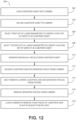
- FIG. 12 shows a flow chart of an example process 200 of fabricating a substrate using a focus line laser and/or a short pulse laser to cut and/or drill a substrate, such as a glass sheet substrate.
- a substrate sheet is loaded into a carrier in operation 202.
- the system has stages that move the laser with respect to the glass by moving the glass or the optical delivery (or both).
- the substrate sheet for example, may comprise one or more discrete substrate sheets or a continuous web of substrate sheet material (e.g., fed from one or more rollers of the system).
- the substrate sheet is secured to a carrier, such as via a vacuum chuck.
- a first particular set of laser parameters are selected in operation 206 to create one or more specific internal defects (e.g., a first set of defects) corresponding to a desired shape, depth, size or other characteristic of the internal defect.
- a second particular set of laser parameters are selected in operation 208 to create one or more specific external defects (e.g., a second set of defects forming a boundary or perimeter around one or more desired individual components) corresponding to a desired shape, depth, size or other characteristic of the external defect.
- Individual shapes are separated from the substrate, such as via using a CO 2 laser, in operation 210.
- the substrate/separated pieces are released from the carrier in operation 212, such as by releasing the vacuum chuck.
- the carrier and pieces cut from the substrate sheet are ejected or otherwise removed from the system in operation 214, and the separated pieces are removed from the carrier in operation 216 by an automated and/or manual operation.
- the carrier is cleaned to remove scrap pieces of the substrate and placed in a queue to be re-used in operation 218.
- the order of the operations shown in FIG. 12 is merely an example.
- the cutting and drilling operations may be performed in either order on the same or different equipment as described herein. Further, as described above, depending on the characteristics of a particular substrate, the separation operation may or may not be performed with an additional CO 2 laser.
- the properties of the cut glass edge are adequate without further grinding, beveling, and polishing. This reduces the amount of time and cost to produce the same product and eliminates any yield losses due to these processes. Furthermore, the number of washing steps is reduced. For the traditional process, a wash step is required after the wafers are cut and ground to remove mechanical debris. This step may be removed by the above process.
- this also has an advantage of greatly increased positional accuracy between the exterior features and the hole pattern (e.g., interposer holes).
- the total accuracy of a pattern placement to true center of a part is of order 200 um.
- the errors can be large even if a vision system is used to find the part edges before hole drilling.
- the process described herein is able to create a laser processed part has much more precision an accuracy of exterior dimensions when compared to a mechanical ground and polish part. Hence cutting and drilling becomes not only a time savings feature but can significantly improve the accuracy specifications of the part, to absolute tolerances of approximately ⁇ 5 um.
- Another advantage of processing a large sheet to make a series of individual parts is that the speed of the drilling process is limited by the speed the beam can be moved relative to the glass, not by the physics of the drilling process itself. If the process of moving glass is broken down further, the most time is taken up in the acceleration and deceleration stage. By combining many parts with the same pattern, the effective time per part can be reduced. By combining many parts on a panel, overall drill speed is increased when the laser beam is scanned across a large panel - there are fewer acceleration/deceleration events as are needed when handling only small parts.
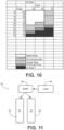
- FIGS. 13 and 14 show that multiple wafers 222 and panels 224 with one or more desired patterns can be created out of a single larger panel 220.
- the laser process would be used to create a first set of defects corresponding to a hole pattern (e.g., pilot holes, vias, interposers or the like) and to create a second set of defects forming a boundary or perimeter such as forming a wafer contour, including any alignment fiducials within the part contours.
- This exterior wafer pattern of the second set of defects could be released using a separate laser process (e.g. CO 2 laser thermal separation) or released in a downstream process (acid etch).
- exterior boundaries or perimeters of individual wafers 222 ( FIG. 13 ) and individual panels 224 are formed by a second set of defects disposed in a generally circular boundary or perimeter for the wafers 222 and in a generally rectangular boundary or perimeter of the panels 224.
- a first set of defects provides interior holes (e.g., pilot holes, vias, interposers or the like) shown disposed within the boundaries or perimeters of the individual wafers 222 and panels 224.
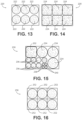
- FIG. 15 depicts an example layout, where one sheet of glass is being cut into four different sizes with two different patterns. This is a particular advantage of a cut and drill process described herein, as the inventory of glass is simplified and the process is very versatile.
- one panel 232, three 300 mm wafers 234, seven 150 mm wafers 236, and two 100mm wafers 238 with a first pattern and two 100 mm wafers 240 with a second distinct pattern could be drilled at the same time from the single substrate sheet 230.
- a single large sheet of glass can be loaded and processed, instead of loading many individual wafers or sub-panels.
- exterior boundaries or perimeters of individual wafers 234, 236, 238 and 240 and individual panels 232 are formed by a second set of defects disposed in a generally circular boundary or perimeter for the wafers 234, 236, 238 and 240 and in a generally rectangular boundary or perimeter of the panels 232.
- a first set of defects provides interior holes (e.g., pilot holes, vias, interposers or the like) shown disposed within the boundaries or perimeters of the individual wafers and panels.
- FIG. 16 shows that multiple subpanels 252 that contain wafers with a desired pattern can be created out of a single larger panel 250.
- the laser process would be used to create an interposer pattern, such as via a first set of defects, and to create a wafer contour, including any alignment fiducials, such as via a second set of defects disposed forming a boundary or perimeter around the first set of defects.
- the laser process may be used to create the subpanels 252. This subpanelpattern could be released using a separate laser process or released in a downstream process such as an acid etch.
- FIG. 17 schematically shows a process with feedstock supplied via a spool of substrate sheet (e.g., glass substrate sheet, such as Corning Willow glass).
- substrate sheet e.g., glass substrate sheet, such as Corning Willow glass.
- the ability to accept rolls decreases material handling and the need to convert rolls to panels.
- the system may perform cut, drill, and release processes. On the exit side of this system, a pick and place may be used to convey the desired parts away.
- the substrate sheet 302 is provided in a spool 304 prior to processing.
- the term "substrate sheet” means a glass substrate sheet, a fused silica sheet, a sapphire sheet, a glass-ceramic substrate sheet, or a ceramic sheet.
- the glass substrate sheet may be fabricated from any glass material capable of being laser drilled and etched as described herein.
- the glass-ceramic substrate sheet and the ceramic substrate sheet may be fabricated from any glass-ceramic or ceramic material capable of being laser drilled and etched as described herein.
- Example glass compositions would be Corning Eagle XG glass, or Corning Gorilla glass compositions such as Corning codes 2318, 2319 and 2320. Partially cerammed materials, such as those that have less than about 20% transmission loss for a particular laser may also be used.
- the substrate sheet 302 is capable of being drilled by a laser drilling process to create a first set of defects adapted to provide one or more pilot holes, vias, interposers or the like and a second set of defects or perforations disposed along a boundary or perimeter surrounding the first set of defects. Accordingly, the substrate sheet 302 should be capable of receiving thermal energy with minimal dimensional change so that substrate sheet 302 does not need to be secured to a support frame during laser processing.
- polyimide film typically used for high temperature electronics applications may experience unpredictable distortion in the range of 10 ⁇ m to 100 ⁇ m when subjected to thermal cycles.
- the substrates described herein, such as glass substrates do not have detectable distortion when subjected to the same thermal cycles.
- the substrate sheet 302 should be capable of withstanding temperatures greater than about 500°C, have a Young's modulus greater than about 50 GPa, and have a hardness of greater than about 3 GPa.
- the substrate sheet 302 should have a thickness such that it is capable of being rolled into a spool, as shown in FIG. 17 .
- the substrate sheet 302 may have a thickness of less than 300 ⁇ m. It should be understood that the substrate sheet 302 may take on other thicknesses depending on the composition and properties of the material.
- the spool 304 is disposed on a spool assembly (not numbered) that mechanically rotates to unroll the substrate sheet 302, as depicted in FIG. 17 .
- the spool assembly, as well as the other spool assemblies described herein, may be configured as any device capable of rotating and having the substrate sheet 302 rolled thereon.
- the substrate sheet 302 passes through a laser processing assembly 306 as it is unrolled from the spool 304.
- the laser processing assembly 306 comprises one or more lasers operable to laser-drill a plurality of defects (not shown in FIG. 17 ) on or through the substrate sheet 302 for cutting (e.g., a second set of defects) and/or drilling (e.g., a first set of defects) the substrate sheet 302.
- the defects may be through-holes, blind holes, defect lines, or damaged areas within the glass substrate formed by multi-photon absorption, as described in more detail below. Any laser process capable of forming laser-induced defects within the substrate sheet 302 may be utilized, depending on the end application and hole requirements.
- the one or more lasers may be operable to produce a laser beam in the ultra-violet or infrared wavelength range.
- Example, non-limiting laser processing assemblies are illustrated in FIGS. 1 , 2A and 2B and described in detail above.
- the spool 304 may include several rolled substrate sheets so that the multiple substrate sheets may be laser drilled simultaneously when arranged in a stacked relationship within the laser processing assembly 306.
- the substrate sheet 302 exits the laser processing assembly 306 already separated into individual component parts 308, 310.
- the separation along perforations / defect lines may occur downstream of the laser processing assembly 306.
- the substrate sheet 302 is shown as a continuous sheet disposed on a roll, the substrate sheet may also be introduced into the laser processing assembly 306 in discrete substrate sheets for processing within the laser processing assembly 306.
- the process 300 may also include an etching process (e.g., for finishing holes within the substrate sheet) that is disposed within the laser processing assembly 306, in series with the laser processing assembly 306 or in a separate discrete location of the system/process downstream of the process 300 shown in FIG. 17 .
- an etching assembly the substrate sheet or the discrete separated parts may be subjected to an etching process to open the defects created by the laser process to form the desired holes. Any known or yet-to-be developed etching process may be utilized to open or otherwise shape the holes into the desired shape.
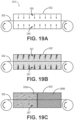
- Example, not-limiting etching processes are schematically depicted in FIGS. 19A-19C and described in detail below. FIG.
- FIG. 20A depicts a plurality of holes 320 in a portion of a substrate sheet 302 following the etching process.
- the cross-sectional shape of the holes can vary from cylindrical, conical, or other shape depending on the application requirements.
- FIG. 20B shows the substrate sheet 302 after the plurality of holes 320 have been filled with a metallization layer forming metallized contact pads 322 outside metal-filled holes 320.
- FIG. 18 shows schematically a roll to roll process 330, where an entire roll 334 of feedstock 332 is perforated and drilled in processing area 336 but not released, and is spooled 338 back up after the laser perforation.
- a release operation 340 e.g. CO2 laser exposure
- the resulting part is identical and has all the desirable properties already outlined.
- the drilled and cut spool could then be acid etched and drop out the desired shape or run through a subsequent process, labeled "Release" in FIG.
- the overall throughput per production line could be much higher, making for lower capital investment per unit of throughput.
- one embodiment could be five machines each perforating contours and drilling five different rolls stock. These five rolls of cut and drilled stock would be sent to a single separation machine, which takes the spools and releases the parts.
- example etching processes 350 that may be provided by an etching assembly 352 are schematically illustrated.
- any etching process capable of opening the laser drilled holes in the substrate sheet 302 may be used.
- the example etching assembly 352 is configured to etch the advancing substrate sheet 302 by spray etching.
- a plurality of nozzles (not shown) directs a plurality of spray jets 355 of etching solution at the substrate sheet 302.
- FIG. 19A illustrates spray jets 355 on both sides of the substrate sheet 302, embodiments may also only direct spray jets 355 on one side of the substrate sheet 302.
- the fluid velocity of the spray jets 355 may vary along the length of the etching assembly 352.
- FIG. 19B schematically illustrates an etching assembly 352' providing aqueous etching where in the substrate sheet 302 is submerged in etching solution.
- any etching solution chemistry may be used depending on the properties of the substrate sheet 302.
- etchant-resistant rollers may be provided in the etching assembly 352' to push the substrate sheet 302 downward such that it is fully submerged in the etching solution.
- optical ultrasonic energy and/or agitation represented by shapes 357) may be applied to the etching solution and/or the substrate sheet 302 to further encourage etching of the holes.
- FIG. 19C schematically illustrates an etching assembly 352" providing multiple etching zones in the form of etching zones 359A and 359B.
- etching zone 359A is an aqueous etching zone (which may or may not provide ultrasonic energy or agitation) while subsequent etching zone 359B is a dry etching zone.
- etching zones may be provided in lieu of, or in addition to, illustrated etching zones 359A and 359B.
- the etching zones may provide spray processes or substrate submersion.
- the different etching zones may be optimized specifically with different etch conditions. Fast changes in etch conditions is difficult to achieve in batch processing where individual sheets of substrates are etched. However, in a continuous or roll-to-roll process as described herein, sequential sets of spray nozzle can vary the etch composition, provide a water rinse, change temperature, add or remove agitation, and the like as the substrate sheet 302 advances through the etching assembly 352.
- each surface of the substrate sheet 302 may be processed independently.
- both surfaces of the substrate sheet 302 can be etched the same or differently.
- only one surface of the substrate sheet 302 may be etched.
- the processing of each surface of the substrate may also be staggered.
- the etch conditions may also be varied across the horizontal width of the substrate.
- etching can eliminate or reduce flaws in the substrate sheet to thereby increase bend strength. Etching near the edges can also produce a rounded, tapered, or varying thickness edge profile.
- the etching process produces a thinning of the substrate sheet as well. This thinning can be uniform over the substrate sheet width or it could more aggressively create thinner regions in the substrate sheet for mechanical or device functionality purposes. These variations are possible by varying the etch conditions across the substrate surface or by masking techniques.
- the substrate sheet 302 may be separated into individual segments after the laser process. Rather than roll-to-roll processing, the individual segments of the substrate sheet 302 may be continuously passed through the etching assemblies described herein. In some embodiments, the substrate sheet 302 may enter the etching assembly 104 as an unrolled sheet, and then be rolled into a spool after passing through the etching assembly.
- FIG. 21 schematically illustrates a portion of a final spool 360 of a rolled substrate sheet 302.
- a gap should be present between adjacent surfaces of the substrate sheet 302.
- an etchant-resistant interleaf layer 361 is disposed between adjacent surfaces of the substrate sheet 302.
- the interleaf layer 361 may be applied before or after the laser processing assembly 306.
- the final spool 360 may also include a plurality of substrate sheets and a plurality of interleaf layers.
- the substrate sheet 302 is placed into an etching assembly 362 as indicated by arrow B.
- the etching solution chemistry and etching duration will depend on the material of the substrate sheet 302 and the desired properties (e.g., hole diameter, substrate sheet thickness, and the like).
- the resulting product is a spool of a rolled substrate sheet having holes formed therein.
- the final spool 360 may be cleaned (e.g., aqueous cleaning or plasma cleaning) and/or subjected to further processing.
- the final spool 360 may be easily packaged and shipped to another facility for further processing.
- a system and process of cutting and drilling in a target substrate uses a pulsed laser and an optical system to generate a line focus of the laser beam within the target substrate, such as a glass substrate sheet.
- the pulsed laser cutting and drilling system and process creates holes or defects that, in certain embodiments, extend the full depth of the glass sheet with each individual laser pulse, and allows the laser system to cut and separate the target substrate into any desired contour by creating a series of perforations that form a contour or desired part shape. Since a glass substrate sheet is brittle, cracking will then follow the perforated contour, allowing the glass substrate sheet to separate into any required shape defined by the perforations.
- the system and process can cut a multitude of glass compositions, ranging from high stress glasses (e.g. ion-exchanged) to low stress glasses (e.g. Corning EXG) at high speeds (>500mm/s), allowing cutting complex shapes with tight radii and complex contours.
- high stress glasses e.g. ion-exchanged
- low stress glasses e.g. Corning EXG
- the system and process can further be adapted to make a desired interposer pilot hole patterns in glass wafers.
- An acid etch process may also be used to enlarge the holes and turn these wafers into suitable glass interposers.
Landscapes
- Engineering & Computer Science (AREA)
- Chemical & Material Sciences (AREA)
- Physics & Mathematics (AREA)
- Optics & Photonics (AREA)
- General Chemical & Material Sciences (AREA)
- Chemical Kinetics & Catalysis (AREA)
- Organic Chemistry (AREA)
- Materials Engineering (AREA)
- Mechanical Engineering (AREA)
- Plasma & Fusion (AREA)
- Geochemistry & Mineralogy (AREA)
- Life Sciences & Earth Sciences (AREA)
- General Physics & Mathematics (AREA)
- Computer Hardware Design (AREA)
- Microelectronics & Electronic Packaging (AREA)
- Condensed Matter Physics & Semiconductors (AREA)
- Power Engineering (AREA)
- Oil, Petroleum & Natural Gas (AREA)
- Ceramic Engineering (AREA)
- Manufacturing & Machinery (AREA)
- Laser Beam Processing (AREA)
- Re-Forming, After-Treatment, Cutting And Transporting Of Glass Products (AREA)
- Surface Treatment Of Glass (AREA)
Applications Claiming Priority (2)
| Application Number | Priority Date | Filing Date | Title |
|---|---|---|---|
| US201562190823P | 2015-07-10 | 2015-07-10 | |
| PCT/US2016/041485 WO2017011296A1 (en) | 2015-07-10 | 2016-07-08 | Methods of continuous fabrication of holes in flexible substrate sheets and products relating to the same |
Publications (2)
| Publication Number | Publication Date |
|---|---|
| EP3319911A1 EP3319911A1 (en) | 2018-05-16 |
| EP3319911B1 true EP3319911B1 (en) | 2023-04-19 |
Family
ID=56550361
Family Applications (1)
| Application Number | Title | Priority Date | Filing Date |
|---|---|---|---|
| EP16742508.1A Revoked EP3319911B1 (en) | 2015-07-10 | 2016-07-08 | Methods of continuous fabrication of holes in flexible substrate sheets and products relating to the same |
Country Status (7)
Families Citing this family (54)
| Publication number | Priority date | Publication date | Assignee | Title |
|---|---|---|---|---|
| FR3024137B1 (fr) * | 2014-07-24 | 2016-07-29 | Saint Gobain | Procede de fabrication de feuilles de verre de forme complexe |
| WO2016138054A1 (en) | 2015-02-27 | 2016-09-01 | Corning Incorporated | Optical assembly having microlouvers |
| TW201713605A (zh) * | 2015-08-21 | 2017-04-16 | 康寧公司 | 用於大量處理基板卷材之系統及方法 |
| US10410883B2 (en) | 2016-06-01 | 2019-09-10 | Corning Incorporated | Articles and methods of forming vias in substrates |
| US10134657B2 (en) | 2016-06-29 | 2018-11-20 | Corning Incorporated | Inorganic wafer having through-holes attached to semiconductor wafer |
| US10794679B2 (en) | 2016-06-29 | 2020-10-06 | Corning Incorporated | Method and system for measuring geometric parameters of through holes |
| US20180018493A1 (en) * | 2016-07-14 | 2018-01-18 | Keycore Technology Corp. | Fingerprint identification device and manufacturing method thereof |
| WO2018020145A1 (fr) * | 2016-07-25 | 2018-02-01 | Amplitude Systemes | Procédé et appareil pour la découpe de matériaux par multi-faisceaux laser femtoseconde |
| US11203183B2 (en) | 2016-09-27 | 2021-12-21 | Vaon, Llc | Single and multi-layer, flat glass-sensor structures |
| US10821707B2 (en) * | 2018-05-17 | 2020-11-03 | Vaon, Llc | Multi-layer, flat glass structures |
| US11243192B2 (en) | 2016-09-27 | 2022-02-08 | Vaon, Llc | 3-D glass printable hand-held gas chromatograph for biomedical and environmental applications |
| US10073305B2 (en) * | 2016-10-07 | 2018-09-11 | Keycore Technology Corp. | Liquid crystal device with fingerprint identification function |
| US10073288B2 (en) * | 2016-10-07 | 2018-09-11 | Keycore Technology Corp. | Liquid crystal module with fingerprint identification function |
| US11608291B2 (en) | 2016-11-04 | 2023-03-21 | Corning Incorporated | Micro-perforated panel systems, applications, and methods of making micro-perforated panel systems |
| JP7217585B2 (ja) | 2017-04-13 | 2023-02-03 | 株式会社ディスコ | 分割方法 |
| US11078112B2 (en) | 2017-05-25 | 2021-08-03 | Corning Incorporated | Silica-containing substrates with vias having an axially variable sidewall taper and methods for forming the same |
| US10580725B2 (en) | 2017-05-25 | 2020-03-03 | Corning Incorporated | Articles having vias with geometry attributes and methods for fabricating the same |
| US11425826B2 (en) | 2017-07-11 | 2022-08-23 | Corning Incorporated | Tiled displays and methods of manufacturing the same |
| US10919794B2 (en) | 2017-12-04 | 2021-02-16 | General Atomics | Method of cutting glass using a laser |
| US12180108B2 (en) | 2017-12-19 | 2024-12-31 | Corning Incorporated | Methods for etching vias in glass-based articles employing positive charge organic molecules |
| US11554984B2 (en) | 2018-02-22 | 2023-01-17 | Corning Incorporated | Alkali-free borosilicate glasses with low post-HF etch roughness |
| US10424606B1 (en) | 2018-04-05 | 2019-09-24 | Corning Incorporated | Systems and methods for reducing substrate surface disruption during via formation |
| US11152294B2 (en) | 2018-04-09 | 2021-10-19 | Corning Incorporated | Hermetic metallized via with improved reliability |
| US11344973B2 (en) | 2018-04-19 | 2022-05-31 | Corning Incorporated | Methods for forming holes in substrates |
| US11059131B2 (en) | 2018-06-22 | 2021-07-13 | Corning Incorporated | Methods for laser processing a substrate stack having one or more transparent workpieces and a black matrix layer |
| KR102742290B1 (ko) * | 2018-07-30 | 2024-12-12 | 코닝 인코포레이티드 | 단열 창 유닛 |
| US12200875B2 (en) | 2018-09-20 | 2025-01-14 | Industrial Technology Research Institute | Copper metallization for through-glass vias on thin glass |
| CN113039040A (zh) * | 2018-10-04 | 2021-06-25 | 康宁公司 | 用于形成多区段显示器的系统和方法 |
| DE102018220240A1 (de) * | 2018-11-20 | 2020-05-20 | Flabeg Deutschland Gmbh | Verfahren zum Vereinzeln eines Glaselements in eine Mehrzahl von Glasbauteilen und Schneidsystem zur Durchführung des Verfahrens |
| US11760682B2 (en) | 2019-02-21 | 2023-09-19 | Corning Incorporated | Glass or glass ceramic articles with copper-metallized through holes and processes for making the same |
| TW202103830A (zh) * | 2019-03-25 | 2021-02-01 | 美商康寧公司 | 在玻璃中形成穿孔之方法 |
| KR102728430B1 (ko) * | 2019-05-14 | 2024-11-08 | 쇼오트 글라스 테크놀로지스 (쑤저우) 코퍼레이션 리미티드. | 높은 굽힘 강도의 박형 유리 기판 및 이의 제조 방법 |
| DE102019003822A1 (de) * | 2019-06-02 | 2020-12-03 | Keming Du | Verfahren zur Bearbeitung transparenter Materialien |
| JP7264461B2 (ja) * | 2019-06-05 | 2023-04-25 | 株式会社Nsc | 平面ガラスアンテナの製造方法。 |
| CN110640337B (zh) * | 2019-08-20 | 2021-06-22 | 江苏大学 | 一种液态流动涂层辅助激光背向湿刻加工低锥度玻璃深孔的装置及方法 |
| CN110526564A (zh) * | 2019-09-16 | 2019-12-03 | 蓝思科技(长沙)有限公司 | 一种玻璃裂片方法 |
| CN110773871B (zh) * | 2019-11-08 | 2021-10-12 | 合肥工业大学 | 一种在空速管的非平表面上制备防结冰表面的制备方法 |
| DE102019219462A1 (de) * | 2019-12-12 | 2021-06-17 | Flabeg Deutschland Gmbh | Verfahren zum Schneiden eines Glaselements und Schneidsystem |
| CN113119285A (zh) * | 2020-01-16 | 2021-07-16 | 大族激光科技产业集团股份有限公司 | 陶瓷工件激光打磨砂的方法 |
| WO2022055671A1 (en) * | 2020-09-09 | 2022-03-17 | Corning Incorporated | Glass substrates with blind vias having depth uniformity and methods for forming the same |
| CN112192325B (zh) * | 2020-10-09 | 2022-04-15 | 北京理工大学 | 飞秒激光在透明硬脆材料上加工微纳米尺度通孔的方法 |
| JP7354084B2 (ja) * | 2020-11-17 | 2023-10-02 | Towa株式会社 | レーザ加工装置及び加工品の製造方法 |
| JP2022119546A (ja) * | 2021-02-04 | 2022-08-17 | 株式会社Nsc | 識別コード付きガラス基板およびその製造方法 |
| CN112992880B (zh) * | 2021-04-25 | 2023-08-15 | 江西沃格光电股份有限公司 | 一种Mini-LED背光板通孔的形成方法及电子设备 |
| EP4086030B1 (en) | 2021-05-07 | 2025-01-22 | Infineon Technologies AG | Method for separating substrates |
| CN113371989A (zh) * | 2021-05-26 | 2021-09-10 | 苏州镭明激光科技有限公司 | 一种半导体芯片的裂片方法及裂片装置 |
| KR102687819B1 (ko) * | 2021-12-20 | 2024-07-24 | 디아이티 주식회사 | 베셀 빔을 이용한 절단 시스템 |
| CN114274384A (zh) * | 2021-12-24 | 2022-04-05 | 唐山国芯晶源电子有限公司 | 一种石英晶圆的切割工艺方法 |
| EP4523837A4 (en) * | 2022-05-10 | 2025-09-10 | Philoptics Co Ltd | METHOD FOR FORMING A PRECISE THROUGH HOLE AT HIGH SPEED USING AN INFRARED LASER |
| CN115073015A (zh) * | 2022-06-24 | 2022-09-20 | 河北光兴半导体技术有限公司 | 玻璃盖板的加工方法 |
| CN115385563A (zh) * | 2022-08-11 | 2022-11-25 | 合肥金龙浩科技有限公司 | 一种手机后盖加工工艺 |
| CN115555740A (zh) * | 2022-10-08 | 2023-01-03 | 苏州科韵激光科技有限公司 | 一种玻璃面板钻孔装置及钻孔方法 |
| CN115876108B (zh) * | 2023-03-01 | 2023-10-24 | 菲特(天津)检测技术有限公司 | 内径测量方法、装置及计算机可读存储介质 |
| CN116638198B (zh) * | 2023-05-25 | 2024-08-09 | 深圳市盛三友电子有限公司 | 高精度偏光片边缘检测装置、偏光片开孔方法及加工方法 |
Citations (15)
| Publication number | Priority date | Publication date | Assignee | Title |
|---|---|---|---|---|
| WO2012006736A2 (en) | 2010-07-12 | 2012-01-19 | Filaser Inc. | Method of material processing by laser filamentation |
| WO2014022356A1 (en) | 2012-07-30 | 2014-02-06 | Raydiance, Inc. | Cutting of brittle materials with tailored edge shape and roughness |
| WO2014022681A1 (en) | 2012-08-01 | 2014-02-06 | Gentex Corporation | Assembly with laser induced channel edge and method thereof |
| US20140199519A1 (en) | 2013-01-15 | 2014-07-17 | Corning Laser Technologies GmbH | Method and device for the laser-based machining of sheet-like substrates |
| WO2014130830A1 (en) | 2013-02-23 | 2014-08-28 | Raydiance, Inc. | Shaping of brittle materials with controlled surface and bulk properties |
| US20150038313A1 (en) | 2013-08-02 | 2015-02-05 | Rofin-Sinar Technologies Inc. | Method and apparatus for performing laser filamentation within transparent materials |
| WO2015018425A1 (de) | 2013-08-07 | 2015-02-12 | Trumpf Laser- Und Systemtechnik Gmbh | Verfahren zum bearbeiten eines plattenartigen werkstückes mit einer transparenten, gläsernen, glasartigen, keramischen und/oder kristallinen lage, trennvorrichtung für ein derartiges werkstück sowie produkt aus einem derartigen werkstück |
| US20150122656A1 (en) | 2013-11-04 | 2015-05-07 | Rofin-Sinar Technologies Inc. | Mass based filtration devices and method of fabrication using bursts of ultrafast laser pulses |
| US20150166395A1 (en) | 2013-12-17 | 2015-06-18 | Corning Incorporated | Method for Rapid Laser Drilling of Holes in Glass and Products Made Therefrom |
| WO2015095151A2 (en) | 2013-12-17 | 2015-06-25 | Corning Incorporated | Laser processing of slots and holes |
| WO2015095091A1 (en) | 2013-12-17 | 2015-06-25 | Corning Incorporated | Laser cut composite glass article and method of cutting |
| WO2015095014A1 (en) | 2013-12-17 | 2015-06-25 | Corning Incorporated | Transparent material cutting with ultrafast laser and beam optics |
| EP2910532A1 (en) | 2013-11-19 | 2015-08-26 | Rofin-Sinar Technologies, Inc. | Method of machining and releasing closed forms from a transparent substrate using burst of ultrafast laser pulses |
| WO2016114934A1 (en) | 2015-01-13 | 2016-07-21 | Rofin-Sinar Technologies Inc. | Method and system for scribing brittle material followed by chemical etching |
| EP2781296B1 (de) | 2013-03-21 | 2020-10-21 | Corning Laser Technologies GmbH | Vorrichtung und verfahren zum ausschneiden von konturen aus flächigen substraten mittels laser |
Family Cites Families (482)
| Publication number | Priority date | Publication date | Assignee | Title |
|---|---|---|---|---|
| US1790397A (en) | 1931-01-27 | Glass workins machine | ||
| US2682134A (en) | 1951-08-17 | 1954-06-29 | Corning Glass Works | Glass sheet containing translucent linear strips |
| US2749794A (en) | 1953-04-24 | 1956-06-12 | Corning Glass Works | Illuminating glassware and method of making it |
| US2932087A (en) | 1954-05-10 | 1960-04-12 | Libbey Owens Ford Glass Co | Template cutting apparatus for bent sheets of glass or the like |
| GB1242172A (en) | 1968-02-23 | 1971-08-11 | Ford Motor Co | A process for chemically cutting glass |
| US3647410A (en) | 1969-09-09 | 1972-03-07 | Owens Illinois Inc | Glass ribbon machine blow head mechanism |
| US3775084A (en) | 1970-01-02 | 1973-11-27 | Owens Illinois Inc | Pressurizer apparatus for glass ribbon machine |
| US3729302A (en) | 1970-01-02 | 1973-04-24 | Owens Illinois Inc | Removal of glass article from ribbon forming machine by vibrating force |
| US3695498A (en) | 1970-08-26 | 1972-10-03 | Ppg Industries Inc | Non-contact thermal cutting |
| US3695497A (en) | 1970-08-26 | 1972-10-03 | Ppg Industries Inc | Method of severing glass |
| DE2231330A1 (de) | 1972-06-27 | 1974-01-10 | Agfa Gevaert Ag | Verfahren und vorrichtung zur erzeugung eines scharfen fokus |
| DE2757890C2 (de) | 1977-12-24 | 1981-10-15 | Fa. Karl Lutz, 6980 Wertheim | Verfahren und Vorrichtung zum Herstellen von Behältnissen aus Röhrenglas, insbesondere Ampullen |
| US4441008A (en) | 1981-09-14 | 1984-04-03 | Ford Motor Company | Method of drilling ultrafine channels through glass |
| US4546231A (en) | 1983-11-14 | 1985-10-08 | Group Ii Manufacturing Ltd. | Creation of a parting zone in a crystal structure |
| JPS6174794A (ja) | 1984-09-17 | 1986-04-17 | Mitsubishi Electric Corp | レ−ザ加工装置の加工ヘツド |
| JPS6246930A (ja) | 1985-08-21 | 1987-02-28 | Bandou Kiko Kk | ガラス板の割断装置 |
| US4646308A (en) | 1985-09-30 | 1987-02-24 | Spectra-Physics, Inc. | Synchronously pumped dye laser using ultrashort pump pulses |
| US4749400A (en) | 1986-12-12 | 1988-06-07 | Ppg Industries, Inc. | Discrete glass sheet cutting |
| DE3789858T2 (de) | 1986-12-18 | 1994-09-01 | Nippon Sheet Glass Co Ltd | Platten für Lichtkontrolle. |
| JPS63192561A (ja) | 1987-02-04 | 1988-08-09 | Nkk Corp | マルチ切断装置 |
| US5104523A (en) | 1987-05-29 | 1992-04-14 | Nippon Sheet Glass Co., Ltd. | Glass-plate sorting system |
| US4918751A (en) | 1987-10-05 | 1990-04-17 | The University Of Rochester | Method for optical pulse transmission through optical fibers which increases the pulse power handling capacity of the fibers |
| IL84255A (en) | 1987-10-23 | 1993-02-21 | Galram Technology Ind Ltd | Process for removal of post- baked photoresist layer |
| JPH01179770A (ja) | 1988-01-12 | 1989-07-17 | Hiroshima Denki Gakuen | 金属とセラミックスとの接合方法 |
| US4764930A (en) | 1988-01-27 | 1988-08-16 | Intelligent Surgical Lasers | Multiwavelength laser source |
| US4907586A (en) | 1988-03-31 | 1990-03-13 | Intelligent Surgical Lasers | Method for reshaping the eye |
| US4929065A (en) | 1988-11-03 | 1990-05-29 | Isotec Partners, Ltd. | Glass plate fusion for macro-gradient refractive index materials |
| US4891054A (en) | 1988-12-30 | 1990-01-02 | Ppg Industries, Inc. | Method for cutting hot glass |
| US5112722A (en) | 1989-04-12 | 1992-05-12 | Nippon Sheet Glass Co., Ltd. | Method of producing light control plate which induces scattering of light at different angles |
| US5104210A (en) | 1989-04-24 | 1992-04-14 | Monsanto Company | Light control films and method of making |
| US5035918A (en) | 1989-04-26 | 1991-07-30 | Amp Incorporated | Non-flammable and strippable plating resist and method of using same |
| US5040182A (en) | 1990-04-24 | 1991-08-13 | Coherent, Inc. | Mode-locked laser |
| ATE218904T1 (de) | 1991-11-06 | 2002-06-15 | Shui T Lai | Vorrichtung für hornhautchirurgie |
| US5265107A (en) | 1992-02-05 | 1993-11-23 | Bell Communications Research, Inc. | Broadband absorber having multiple quantum wells of different thicknesses |
| US5410567A (en) | 1992-03-05 | 1995-04-25 | Corning Incorporated | Optical fiber draw furnace |
| JPH05323110A (ja) | 1992-05-22 | 1993-12-07 | Hitachi Koki Co Ltd | 多ビーム発生素子 |
| US6016223A (en) | 1992-08-31 | 2000-01-18 | Canon Kabushiki Kaisha | Double bessel beam producing method and apparatus |
| JP3553986B2 (ja) | 1992-08-31 | 2004-08-11 | キヤノン株式会社 | 2重ベッセルビーム発生方法及び装置 |
| CA2112843A1 (en) | 1993-02-04 | 1994-08-05 | Richard C. Ujazdowski | Variable repetition rate picosecond laser |
| JPH06318756A (ja) | 1993-05-06 | 1994-11-15 | Toshiba Corp | レ−ザ装置 |
| JP3293136B2 (ja) | 1993-06-04 | 2002-06-17 | セイコーエプソン株式会社 | レーザ加工装置及びレーザ加工方法 |
| US5521352A (en) | 1993-09-23 | 1996-05-28 | Laser Machining, Inc. | Laser cutting apparatus |
| US5418803A (en) | 1994-01-11 | 1995-05-23 | American Biogenetic Sciences, Inc. | White light laser technology |
| US6489589B1 (en) | 1994-02-07 | 2002-12-03 | Board Of Regents, University Of Nebraska-Lincoln | Femtosecond laser utilization methods and apparatus and method for producing nanoparticles |
| US5436925A (en) | 1994-03-01 | 1995-07-25 | Hewlett-Packard Company | Colliding pulse mode-locked fiber ring laser using a semiconductor saturable absorber |
| US5400350A (en) | 1994-03-31 | 1995-03-21 | Imra America, Inc. | Method and apparatus for generating high energy ultrashort pulses |
| US5778016A (en) | 1994-04-01 | 1998-07-07 | Imra America, Inc. | Scanning temporal ultrafast delay methods and apparatuses therefor |
| JP2526806B2 (ja) | 1994-04-26 | 1996-08-21 | 日本電気株式会社 | 半導体レ―ザおよびその動作方法 |
| WO1995031023A1 (en) | 1994-05-09 | 1995-11-16 | Massachusetts Institute Of Technology | Dispersion-compensated laser using prismatic end elements |
| US6016324A (en) | 1994-08-24 | 2000-01-18 | Jmar Research, Inc. | Short pulse laser system |
| US5434875A (en) | 1994-08-24 | 1995-07-18 | Tamar Technology Co. | Low cost, high average power, high brightness solid state laser |
| US5638396A (en) | 1994-09-19 | 1997-06-10 | Textron Systems Corporation | Laser ultrasonics-based material analysis system and method |
| US5776220A (en) | 1994-09-19 | 1998-07-07 | Corning Incorporated | Method and apparatus for breaking brittle materials |
| US5578229A (en) | 1994-10-18 | 1996-11-26 | Michigan State University | Method and apparatus for cutting boards using opposing convergent laser beams |
| US5696782A (en) | 1995-05-19 | 1997-12-09 | Imra America, Inc. | High power fiber chirped pulse amplification systems based on cladding pumped rare-earth doped fibers |
| JP3319912B2 (ja) | 1995-06-29 | 2002-09-03 | 株式会社デンソー | 半導体センサ用台座およびその加工方法 |
| JPH09106243A (ja) | 1995-10-12 | 1997-04-22 | Dainippon Printing Co Ltd | ホログラムの複製方法 |
| US5715346A (en) | 1995-12-15 | 1998-02-03 | Corning Incorporated | Large effective area single mode optical waveguide |
| US5736709A (en) | 1996-08-12 | 1998-04-07 | Armco Inc. | Descaling metal with a laser having a very short pulse width and high average power |
| US7353829B1 (en) | 1996-10-30 | 2008-04-08 | Provectus Devicetech, Inc. | Methods and apparatus for multi-photon photo-activation of therapeutic agents |
| US6301932B1 (en) | 1996-11-13 | 2001-10-16 | Corning Incorporated | Method for forming an internally channeled glass article |
| US5781684A (en) | 1996-12-20 | 1998-07-14 | Corning Incorporated | Single mode optical waveguide having large effective area |
| US6156030A (en) | 1997-06-04 | 2000-12-05 | Y-Beam Technologies, Inc. | Method and apparatus for high precision variable rate material removal and modification |
| BE1011208A4 (fr) | 1997-06-11 | 1999-06-01 | Cuvelier Georges | Procede de decalottage de pieces en verre. |
| DE19728766C1 (de) | 1997-07-07 | 1998-12-17 | Schott Rohrglas Gmbh | Verwendung eines Verfahrens zur Herstellung einer Sollbruchstelle bei einem Glaskörper |
| US6078599A (en) | 1997-07-22 | 2000-06-20 | Cymer, Inc. | Wavelength shift correction technique for a laser |
| JP3264224B2 (ja) | 1997-08-04 | 2002-03-11 | キヤノン株式会社 | 照明装置及びそれを用いた投影露光装置 |
| DE19750320C1 (de) | 1997-11-13 | 1999-04-01 | Max Planck Gesellschaft | Verfahren und Vorrichtung zur Lichtpulsverstärkung |
| WO1999029243A1 (en) | 1997-12-05 | 1999-06-17 | Thermolase Corporation | Skin enhancement using laser light |
| US6501578B1 (en) | 1997-12-19 | 2002-12-31 | Electric Power Research Institute, Inc. | Apparatus and method for line of sight laser communications |
| JPH11197498A (ja) | 1998-01-13 | 1999-07-27 | Japan Science & Technology Corp | 無機材料内部の選択的改質方法及び内部が選択的に改質された無機材料 |
| US6272156B1 (en) | 1998-01-28 | 2001-08-07 | Coherent, Inc. | Apparatus for ultrashort pulse transportation and delivery |
| JPH11240730A (ja) | 1998-02-27 | 1999-09-07 | Nec Kansai Ltd | 脆性材料の割断方法 |
| JPH11269683A (ja) | 1998-03-18 | 1999-10-05 | Armco Inc | 金属表面から酸化物を除去する方法及び装置 |
| US6160835A (en) | 1998-03-20 | 2000-12-12 | Rocky Mountain Instrument Co. | Hand-held marker with dual output laser |
| EP0949541B1 (en) | 1998-04-08 | 2006-06-07 | ASML Netherlands B.V. | Lithography apparatus |
| DE69931690T2 (de) | 1998-04-08 | 2007-06-14 | Asml Netherlands B.V. | Lithographischer Apparat |
| US6256328B1 (en) | 1998-05-15 | 2001-07-03 | University Of Central Florida | Multiwavelength modelocked semiconductor diode laser |
| JPH11347861A (ja) | 1998-06-03 | 1999-12-21 | Amada Co Ltd | レーザ加工機における複合加工方法およびレーザ加工機における複合加工システム |
| JPH11347758A (ja) | 1998-06-10 | 1999-12-21 | Mitsubishi Heavy Ind Ltd | 超精密加工装置 |
| TW419867B (en) | 1998-08-26 | 2001-01-21 | Samsung Electronics Co Ltd | Laser cutting apparatus and method |
| DE19851353C1 (de) | 1998-11-06 | 1999-10-07 | Schott Glas | Verfahren und Vorrichtung zum Schneiden eines Laminats aus einem sprödbrüchigen Werkstoff und einem Kunststoff |
| JP3178524B2 (ja) | 1998-11-26 | 2001-06-18 | 住友重機械工業株式会社 | レーザマーキング方法と装置及びマーキングされた部材 |
| US6259058B1 (en) | 1998-12-01 | 2001-07-10 | Accudyne Display And Semiconductor Systems, Inc. | Apparatus for separating non-metallic substrates |
| US7649153B2 (en) | 1998-12-11 | 2010-01-19 | International Business Machines Corporation | Method for minimizing sample damage during the ablation of material using a focused ultrashort pulsed laser beam |
| US6445491B2 (en) | 1999-01-29 | 2002-09-03 | Irma America, Inc. | Method and apparatus for optical sectioning and imaging using time-gated parametric image amplification |
| US6381391B1 (en) | 1999-02-19 | 2002-04-30 | The Regents Of The University Of Michigan | Method and system for generating a broadband spectral continuum and continuous wave-generating system utilizing same |
| DE19908630A1 (de) | 1999-02-27 | 2000-08-31 | Bosch Gmbh Robert | Abschirmung gegen Laserstrahlen |
| DE19983939B4 (de) | 1999-03-05 | 2005-02-17 | Mitsubishi Denki K.K. | Laserstrahlmaschine |
| US6484052B1 (en) | 1999-03-30 | 2002-11-19 | The Regents Of The University Of California | Optically generated ultrasound for enhanced drug delivery |
| EP1043110B1 (en) | 1999-04-02 | 2006-08-23 | Murata Manufacturing Co., Ltd. | Laser method for machining through holes in a ceramic green sheet |
| US6373565B1 (en) | 1999-05-27 | 2002-04-16 | Spectra Physics Lasers, Inc. | Method and apparatus to detect a flaw in a surface of an article |
| CN2388062Y (zh) | 1999-06-21 | 2000-07-19 | 郭广宗 | 一层有孔一层无孔双层玻璃车船窗 |
| US6449301B1 (en) | 1999-06-22 | 2002-09-10 | The Regents Of The University Of California | Method and apparatus for mode locking of external cavity semiconductor lasers with saturable Bragg reflectors |
| US6259151B1 (en) | 1999-07-21 | 2001-07-10 | Intersil Corporation | Use of barrier refractive or anti-reflective layer to improve laser trim characteristics of thin film resistors |
| US6573026B1 (en) | 1999-07-29 | 2003-06-03 | Corning Incorporated | Femtosecond laser writing of glass, including borosilicate, sulfide, and lead glasses |
| US6452117B2 (en) | 1999-08-26 | 2002-09-17 | International Business Machines Corporation | Method for filling high aspect ratio via holes in electronic substrates and the resulting holes |
| DE19952331C1 (de) | 1999-10-29 | 2001-08-30 | Schott Spezialglas Gmbh | Verfahren und Vorrichtung zum schnellen Schneiden eines Werkstücks aus sprödbrüchigem Werkstoff mittels Laserstrahlen |
| JP2001130921A (ja) | 1999-10-29 | 2001-05-15 | Mitsuboshi Diamond Industrial Co Ltd | 脆性基板の加工方法及び装置 |
| JP2001138083A (ja) | 1999-11-18 | 2001-05-22 | Seiko Epson Corp | レーザー加工装置及びレーザー照射方法 |
| JP4592855B2 (ja) | 1999-12-24 | 2010-12-08 | 株式会社半導体エネルギー研究所 | 半導体装置の作製方法 |
| US6339208B1 (en) | 2000-01-19 | 2002-01-15 | General Electric Company | Method of forming cooling holes |
| US6552301B2 (en) | 2000-01-25 | 2003-04-22 | Peter R. Herman | Burst-ultrafast laser machining method |
| WO2001085387A1 (en) | 2000-05-11 | 2001-11-15 | Ptg Precision Technology Center Limited Llc | System for cutting brittle materials |
| DE10030388A1 (de) | 2000-06-21 | 2002-01-03 | Schott Glas | Verfahren zur Herstellung von Glassubstraten für elektronische Speichermedien |
| JP3530114B2 (ja) | 2000-07-11 | 2004-05-24 | 忠弘 大見 | 単結晶の切断方法 |
| JP2002040330A (ja) | 2000-07-25 | 2002-02-06 | Olympus Optical Co Ltd | 光学素子切換え制御装置 |
| JP2002045985A (ja) | 2000-08-07 | 2002-02-12 | Matsushita Electric Ind Co Ltd | レーザ楕円穴加工方法およびレーザ楕円穴加工装置 |
| JP4964376B2 (ja) | 2000-09-13 | 2012-06-27 | 浜松ホトニクス株式会社 | レーザ加工装置及びレーザ加工方法 |
| JP4659300B2 (ja) | 2000-09-13 | 2011-03-30 | 浜松ホトニクス株式会社 | レーザ加工方法及び半導体チップの製造方法 |
| KR100673073B1 (ko) | 2000-10-21 | 2007-01-22 | 삼성전자주식회사 | 레이저 빔을 이용한 비금속 기판의 절단 방법 및 장치 |
| SE0004096D0 (sv) | 2000-11-08 | 2000-11-08 | Nira Automotive Ab | Positioning system |
| US20020110639A1 (en) | 2000-11-27 | 2002-08-15 | Donald Bruns | Epoxy coating for optical surfaces |
| US20020082466A1 (en) | 2000-12-22 | 2002-06-27 | Jeongho Han | Laser surgical system with light source and video scope |
| JP4880820B2 (ja) | 2001-01-19 | 2012-02-22 | 株式会社レーザーシステム | レーザ支援加工方法 |
| JP2002228818A (ja) | 2001-02-05 | 2002-08-14 | Taiyo Yuden Co Ltd | レーザー加工用回折光学素子、レーザー加工装置及びレーザー加工方法 |
| JP2002321081A (ja) | 2001-04-27 | 2002-11-05 | Ishikawajima Harima Heavy Ind Co Ltd | レーザ照射装置及びレーザ照射方法 |
| JP2003007370A (ja) * | 2001-06-19 | 2003-01-10 | Yazaki Corp | 端子金具 |
| SG108262A1 (en) | 2001-07-06 | 2005-01-28 | Inst Data Storage | Method and apparatus for cutting a multi-layer substrate by dual laser irradiation |
| US6754429B2 (en) | 2001-07-06 | 2004-06-22 | Corning Incorporated | Method of making optical fiber devices and devices thereof |
| TWI224382B (en) | 2001-07-12 | 2004-11-21 | Hitachi Ltd | Wiring glass substrate and manufacturing method thereof, conductive paste and semiconductor module used for the same, and conductor forming method |
| JP3775250B2 (ja) | 2001-07-12 | 2006-05-17 | セイコーエプソン株式会社 | レーザー加工方法及びレーザー加工装置 |
| TWI252788B (en) | 2001-08-10 | 2006-04-11 | Mitsuboshi Diamond Ind Co Ltd | Brittle material substrate chamfering method and chamfering device |
| JP3795778B2 (ja) | 2001-08-24 | 2006-07-12 | 株式会社ノリタケカンパニーリミテド | 水添ビスフェノールa型エポキシ樹脂を用いたレジノイド研削砥石 |
| JP4294239B2 (ja) | 2001-09-17 | 2009-07-08 | 日立ビアメカニクス株式会社 | レーザ加工装置および透過型の1/2波長板 |
| JP2003114400A (ja) | 2001-10-04 | 2003-04-18 | Sumitomo Electric Ind Ltd | レーザ光学システムおよびレーザ加工方法 |
| JP2003154517A (ja) | 2001-11-21 | 2003-05-27 | Seiko Epson Corp | 脆性材料の割断加工方法およびその装置、並びに電子部品の製造方法 |
| US6720519B2 (en) | 2001-11-30 | 2004-04-13 | Matsushita Electric Industrial Co., Ltd. | System and method of laser drilling |
| US6973384B2 (en) | 2001-12-06 | 2005-12-06 | Bellsouth Intellectual Property Corporation | Automated location-intelligent traffic notification service systems and methods |
| JP2003238178A (ja) | 2002-02-21 | 2003-08-27 | Toshiba Ceramics Co Ltd | ガス導入用シャワープレート及びその製造方法 |
| ES2356817T3 (es) | 2002-03-12 | 2011-04-13 | Hamamatsu Photonics K.K. | Método de corte de un objeto procesado. |
| US6787732B1 (en) | 2002-04-02 | 2004-09-07 | Seagate Technology Llc | Method for laser-scribing brittle substrates and apparatus therefor |
| US6737345B1 (en) | 2002-09-10 | 2004-05-18 | Taiwan Semiconductor Manufacturing Company | Scheme to define laser fuse in dual damascene CU process |
| JP3929393B2 (ja) | 2002-12-03 | 2007-06-13 | 株式会社日本エミック | 切断装置 |
| JP2004209675A (ja) | 2002-12-26 | 2004-07-29 | Kashifuji:Kk | 押圧切断装置及び押圧切断方法 |
| KR100497820B1 (ko) | 2003-01-06 | 2005-07-01 | 로체 시스템즈(주) | 유리판절단장치 |
| TWI319412B (en) | 2003-01-15 | 2010-01-11 | Sumitomo Rubber Ind | Polymeric-type antistatic agent and antistatic polymer composition and fabricating method thereof |
| JP3775410B2 (ja) | 2003-02-03 | 2006-05-17 | セイコーエプソン株式会社 | レーザー加工方法、レーザー溶接方法並びにレーザー加工装置 |
| EP1609559B1 (en) | 2003-03-12 | 2007-08-08 | Hamamatsu Photonics K. K. | Laser beam machining method |
| US7617167B2 (en) | 2003-04-09 | 2009-11-10 | Avisere, Inc. | Machine vision system for enterprise management |
| WO2004094329A1 (en) | 2003-04-22 | 2004-11-04 | The Coca-Cola Company | Method and apparatus for strengthening glass |
| US7511886B2 (en) | 2003-05-13 | 2009-03-31 | Carl Zeiss Smt Ag | Optical beam transformation system and illumination system comprising an optical beam transformation system |
| FR2855084A1 (fr) | 2003-05-22 | 2004-11-26 | Air Liquide | Optique de focalisation pour le coupage laser |
| JP2005000952A (ja) | 2003-06-12 | 2005-01-06 | Nippon Sheet Glass Co Ltd | レーザー加工方法及びレーザー加工装置 |
| US7492948B2 (en) | 2003-06-26 | 2009-02-17 | Denmarks Tekniske Universitet | Generation of a desired wavefront with a plurality of phase contrast filters |
| EP2269765B1 (en) | 2003-07-18 | 2014-10-15 | Hamamatsu Photonics K.K. | Cut semiconductor chip |
| JP2005104819A (ja) | 2003-09-10 | 2005-04-21 | Nippon Sheet Glass Co Ltd | 合せガラスの切断方法及び合せガラス切断装置 |
| JP2005138143A (ja) | 2003-11-06 | 2005-06-02 | Disco Abrasive Syst Ltd | レーザ光線を利用する加工装置 |
| US7172067B2 (en) | 2003-11-10 | 2007-02-06 | Johnson Level & Tool Mfg. Co., Inc. | Level case with positioning indentations |
| JP2005144487A (ja) | 2003-11-13 | 2005-06-09 | Seiko Epson Corp | レーザ加工装置及びレーザ加工方法 |
| US20080190981A1 (en) | 2003-12-04 | 2008-08-14 | Yasutomo Okajima | Method for Processing Substrate, Apparatus for Processing Substrate, Method for Conveying Substrate and Mechanism for Conveying Substrate |
| US7633033B2 (en) | 2004-01-09 | 2009-12-15 | General Lasertronics Corporation | Color sensing for laser decoating |
| JP4951241B2 (ja) | 2004-01-16 | 2012-06-13 | 独立行政法人科学技術振興機構 | 微細加工方法 |
| JP4074589B2 (ja) | 2004-01-22 | 2008-04-09 | Tdk株式会社 | レーザ加工装置及びレーザ加工方法 |
| KR100813350B1 (ko) | 2004-03-05 | 2008-03-12 | 올림푸스 가부시키가이샤 | 레이저 가공 장치 |
| DE102004012402B3 (de) | 2004-03-13 | 2005-08-25 | Schott Ag | Verfahren zum Freiformschneiden von gewölbten Substraten aus sprödbrüchigem Material |
| JP4418282B2 (ja) | 2004-03-31 | 2010-02-17 | 株式会社レーザーシステム | レーザ加工方法 |
| KR100626554B1 (ko) | 2004-05-11 | 2006-09-21 | 주식회사 탑 엔지니어링 | 비금속재 절단장치 및 비금속재 절단시의 절단깊이 제어방법 |
| US7804043B2 (en) | 2004-06-15 | 2010-09-28 | Laserfacturing Inc. | Method and apparatus for dicing of thin and ultra thin semiconductor wafer using ultrafast pulse laser |
| JP4527488B2 (ja) | 2004-10-07 | 2010-08-18 | 株式会社ディスコ | レーザ加工装置 |
| JP3887394B2 (ja) | 2004-10-08 | 2007-02-28 | 芝浦メカトロニクス株式会社 | 脆性材料の割断加工システム及びその方法 |
| JP3723201B1 (ja) | 2004-10-18 | 2005-12-07 | 独立行政法人食品総合研究所 | 貫通孔を有する金属製基板を用いたマイクロスフィアの製造方法 |
| TW200621661A (en) | 2004-10-25 | 2006-07-01 | Mitsuboshi Diamond Ind Co Ltd | Method and device for forming crack |
| JP4692717B2 (ja) | 2004-11-02 | 2011-06-01 | 澁谷工業株式会社 | 脆性材料の割断装置 |
| JP4222296B2 (ja) | 2004-11-22 | 2009-02-12 | 住友電気工業株式会社 | レーザ加工方法とレーザ加工装置 |
| JP4564343B2 (ja) | 2004-11-24 | 2010-10-20 | 大日本印刷株式会社 | 導電材充填スルーホール基板の製造方法 |
| US7201965B2 (en) | 2004-12-13 | 2007-04-10 | Corning Incorporated | Glass laminate substrate having enhanced impact and static loading resistance |
| KR101096733B1 (ko) | 2004-12-27 | 2011-12-21 | 엘지디스플레이 주식회사 | 기판의 절단장치 및 이를 이용한 기판의 절단방법 |
| WO2006073098A1 (ja) | 2005-01-05 | 2006-07-13 | Thk Co., Ltd. | ワークのブレイク方法及び装置、スクライブ及びブレイク方法、並びにブレイク機能付きスクライブ装置 |
| WO2006082738A1 (ja) | 2005-02-03 | 2006-08-10 | Nikon Corporation | オプティカルインテグレータ、照明光学装置、露光装置、および露光方法 |
| JP2006248885A (ja) | 2005-02-08 | 2006-09-21 | Takeji Arai | 超短パルスレーザによる石英の切断方法 |
| JP2006240948A (ja) | 2005-03-07 | 2006-09-14 | Nippon Sheet Glass Co Ltd | ガラス板製品を切り抜きにより製造する方法 |
| DE102005013783B4 (de) | 2005-03-22 | 2007-08-16 | Jenoptik Automatisierungstechnik Gmbh | Verfahren zum Trennen von spröden Materialien mittels Laser mit unsymmetrischer Strahlungsdichteverteilung |
| US20060261118A1 (en) | 2005-05-17 | 2006-11-23 | Cox Judy K | Method and apparatus for separating a pane of brittle material from a moving ribbon of the material |
| JP4173151B2 (ja) | 2005-05-23 | 2008-10-29 | 株式会社椿本チエイン | コンベヤチェーン |
| JP4490883B2 (ja) | 2005-07-19 | 2010-06-30 | 株式会社レーザーシステム | レーザ加工装置およびレーザ加工方法 |
| DE102005039833A1 (de) | 2005-08-22 | 2007-03-01 | Rowiak Gmbh | Vorrichtung und Verfahren zur Materialtrennung mit Laserpulsen |
| KR20070023958A (ko) | 2005-08-25 | 2007-03-02 | 삼성전자주식회사 | 액정 표시 장치용 기판 절단 시스템 및 상기 시스템을이용한 액정 표시 장치용 기판 절단 방법 |
| US7373041B2 (en) | 2005-08-31 | 2008-05-13 | Schleifring Und Apparatebau Gmbh | Optical rotary coupling |
| US9138913B2 (en) | 2005-09-08 | 2015-09-22 | Imra America, Inc. | Transparent material processing with an ultrashort pulse laser |
| US7626138B2 (en) | 2005-09-08 | 2009-12-01 | Imra America, Inc. | Transparent material processing with an ultrashort pulse laser |
| US8118971B2 (en) | 2005-09-12 | 2012-02-21 | Nippon Sheet Glass Company, Limited | Interlayer film separation method |
| US20070111480A1 (en) | 2005-11-16 | 2007-05-17 | Denso Corporation | Wafer product and processing method therefor |
| JP2007142000A (ja) | 2005-11-16 | 2007-06-07 | Denso Corp | レーザ加工装置およびレーザ加工方法 |
| US7838331B2 (en) | 2005-11-16 | 2010-11-23 | Denso Corporation | Method for dicing semiconductor substrate |
| US7977601B2 (en) | 2005-11-28 | 2011-07-12 | Electro Scientific Industries, Inc. | X and Y orthogonal cut direction processing with set beam separation using 45 degree beam split orientation apparatus and method |
| WO2007069516A1 (en) | 2005-12-16 | 2007-06-21 | Semiconductor Energy Laboratory Co., Ltd. | Laser irradiation apparatus, laser irradiation method, and manufacturing method of semiconductor device |
| JP4483793B2 (ja) | 2006-01-27 | 2010-06-16 | セイコーエプソン株式会社 | 微細構造体の製造方法及び製造装置 |
| US7418181B2 (en) | 2006-02-13 | 2008-08-26 | Adc Telecommunications, Inc. | Fiber optic splitter module |
| JP5245819B2 (ja) | 2006-02-15 | 2013-07-24 | 旭硝子株式会社 | ガラス基板の面取り方法および装置 |
| US7535634B1 (en) | 2006-02-16 | 2009-05-19 | The United States Of America As Represented By The National Aeronautics And Space Administration | Optical device, system, and method of generating high angular momentum beams |
| JP4672689B2 (ja) | 2006-02-22 | 2011-04-20 | 日本板硝子株式会社 | レーザを用いたガラスの加工方法および加工装置 |
| WO2007096958A1 (ja) | 2006-02-22 | 2007-08-30 | Nippon Sheet Glass Company, Limited | レーザを用いたガラスの加工方法および加工装置 |
| US20090176034A1 (en) | 2006-02-23 | 2009-07-09 | Picodeon Ltd. Oy | Surface Treatment Technique and Surface Treatment Apparatus Associated With Ablation Technology |
| JP2007253203A (ja) | 2006-03-24 | 2007-10-04 | Sumitomo Electric Ind Ltd | レーザ加工用光学装置 |
| US20070298529A1 (en) | 2006-05-31 | 2007-12-27 | Toyoda Gosei, Co., Ltd. | Semiconductor light-emitting device and method for separating semiconductor light-emitting devices |
| EP1875983B1 (en) | 2006-07-03 | 2013-09-11 | Hamamatsu Photonics K.K. | Laser processing method and chip |
| DE102006035555A1 (de) | 2006-07-27 | 2008-01-31 | Eliog-Kelvitherm Industrieofenbau Gmbh | Anordnung und Verfahren zur Verformung von Glasscheiben |
| TWI362370B (en) | 2006-08-18 | 2012-04-21 | Foxsemicon Integrated Tech Inc | Method for cutting a brittle substrate |
| US8168514B2 (en) | 2006-08-24 | 2012-05-01 | Corning Incorporated | Laser separation of thin laminated glass substrates for flexible display applications |
| EP2065120B1 (en) | 2006-09-19 | 2015-07-01 | Hamamatsu Photonics K.K. | Laser processing method |
| JP2008132616A (ja) | 2006-11-27 | 2008-06-12 | Shibuya Kogyo Co Ltd | 脆性材料の割断方法とその装置 |
| US8338744B2 (en) | 2006-11-30 | 2012-12-25 | Sumitomo Electric Industries, Ltd. | Condensing optical system, laser processing method and apparatus, and manufacturing method of brittle material blank |
| AT504726A1 (de) | 2007-01-05 | 2008-07-15 | Lisec Maschb Gmbh | Verfahren und vorrichtung zum herstellen eines trennspalts in einer glasscheibe |
| US8952832B2 (en) | 2008-01-18 | 2015-02-10 | Invensense, Inc. | Interfacing application programs and motion sensors of a device |
| JP2008168327A (ja) | 2007-01-15 | 2008-07-24 | Shinko Seisakusho:Kk | レーザ切断装置 |
| US7566657B2 (en) | 2007-01-17 | 2009-07-28 | Hewlett-Packard Development Company, L.P. | Methods of forming through-substrate interconnects |
| JP5318748B2 (ja) | 2007-02-22 | 2013-10-16 | 日本板硝子株式会社 | 陽極接合用ガラス |
| EP2130234B1 (en) | 2007-02-27 | 2014-10-29 | Carl Zeiss Laser Optics GmbH | Continuous coating installation and method for producing crystalline thin films |
| WO2008126742A1 (ja) | 2007-04-05 | 2008-10-23 | Cyber Laser Inc. | レーザ加工方法及び切断方法並びに多層基板を有する構造体の分割方法 |
| EP1983154B1 (en) | 2007-04-17 | 2013-12-25 | Services Pétroliers Schlumberger | In-situ correction of triaxial accelerometer and magnetometer measurements made in a well |
| DE102007018674A1 (de) | 2007-04-18 | 2008-10-23 | Lzh Laserzentrum Hannover E.V. | Verfahren zum Bilden von Durchgangslöchern in Bauteilen aus Glas |
| US8236116B2 (en) | 2007-06-06 | 2012-08-07 | Centre Luxembourgeois De Recherches Pour Le Verre Et Al Ceramique S.A. (C.R.V.C.) | Method of making coated glass article, and intermediate product used in same |
| US20080310465A1 (en) | 2007-06-14 | 2008-12-18 | Martin Achtenhagen | Method and Laser Device for Stabilized Frequency Doubling |
| WO2009012913A1 (de) | 2007-07-21 | 2009-01-29 | Keming Du | Optische anordnung zur erzeugung von multistrahlen |
| US8169587B2 (en) | 2007-08-16 | 2012-05-01 | Apple Inc. | Methods and systems for strengthening LCD modules |
| JP2009056482A (ja) | 2007-08-31 | 2009-03-19 | Seiko Epson Corp | 基板分割方法、及び表示装置の製造方法 |
| US20100276505A1 (en) | 2007-09-26 | 2010-11-04 | Roger Earl Smith | Drilling in stretched substrates |
| WO2009050938A1 (ja) | 2007-10-16 | 2009-04-23 | Mitsuboshi Diamond Industrial Co., Ltd. | 脆性材料基板のu字状溝加工方法およびこれを用いた除去加工方法およびくり抜き加工方法および面取り方法 |
| KR20090041316A (ko) | 2007-10-23 | 2009-04-28 | 가부시키가이샤 한도오따이 에네루기 켄큐쇼 | 성막 방법 및 발광 장치의 제작 방법 |
| KR100949152B1 (ko) | 2007-11-23 | 2010-03-25 | 삼성코닝정밀유리 주식회사 | 유리 기판 레이저 절단 장치 |
| KR20090057161A (ko) | 2007-12-01 | 2009-06-04 | 주식회사 이엔팩 | 초발수성 좌변기 시트 |
| CN101462822B (zh) | 2007-12-21 | 2012-08-29 | 鸿富锦精密工业(深圳)有限公司 | 具有通孔的脆性非金属工件及其加工方法 |
| US20090183764A1 (en) | 2008-01-18 | 2009-07-23 | Tenksolar, Inc | Detachable Louver System |
| JP2009178725A (ja) | 2008-01-29 | 2009-08-13 | Sunx Ltd | レーザ加工装置及びレーザ加工方法 |
| KR101303542B1 (ko) | 2008-02-11 | 2013-09-03 | 엘지디스플레이 주식회사 | 평판표시패널 절단장치 |
| EP2285521B1 (en) | 2008-02-20 | 2019-06-12 | Lasercoil Technologies, LLC | Progressive laser blanking device for high speed cutting |
| US20100319898A1 (en) | 2008-03-13 | 2010-12-23 | Underwood Patrick K | Thermal interconnect and integrated interface systems, methods of production and uses thereof |
| JP5333816B2 (ja) | 2008-03-26 | 2013-11-06 | 旭硝子株式会社 | ガラス板の切線加工装置及び切線加工方法 |
| JP5345334B2 (ja) | 2008-04-08 | 2013-11-20 | 株式会社レミ | 脆性材料の熱応力割断方法 |
| JP5274085B2 (ja) | 2008-04-09 | 2013-08-28 | 株式会社アルバック | レーザー加工装置、レーザービームのピッチ可変方法、及びレーザー加工方法 |
| US8358888B2 (en) | 2008-04-10 | 2013-01-22 | Ofs Fitel, Llc | Systems and techniques for generating Bessel beams |
| US8035901B2 (en) | 2008-04-30 | 2011-10-11 | Corning Incorporated | Laser scoring with curved trajectory |
| HUE037068T2 (hu) | 2008-05-14 | 2018-08-28 | Gerresheimer Glas Gmbh | Eljárás és berendezés automatikus gyártórendszeren szennyezõ szemcsék tartályokból való eltávolítására |
| US8053704B2 (en) | 2008-05-27 | 2011-11-08 | Corning Incorporated | Scoring of non-flat materials |
| JP2009297734A (ja) | 2008-06-11 | 2009-12-24 | Nitto Denko Corp | レーザー加工用粘着シート及びレーザー加工方法 |
| US8514476B2 (en) | 2008-06-25 | 2013-08-20 | View, Inc. | Multi-pane dynamic window and method for making same |
| US7810355B2 (en) | 2008-06-30 | 2010-10-12 | Apple Inc. | Full perimeter chemical strengthening of substrates |
| NL2003157A1 (nl) | 2008-07-11 | 2010-01-12 | Asml Netherlands Bv | Radiation source, lithographic apparatus, and device manufacturing method. |
| JP2010017990A (ja) | 2008-07-14 | 2010-01-28 | Seiko Epson Corp | 基板分割方法 |
| JP5071868B2 (ja) | 2008-08-11 | 2012-11-14 | オムロン株式会社 | レーザ加工方法、レーザ加工装置、光学素子の製造方法、および光学素子 |
| JP5155774B2 (ja) | 2008-08-21 | 2013-03-06 | 株式会社ノリタケカンパニーリミテド | プラトー面加工用レジノイド超砥粒砥石ホイール |
| JP2010075991A (ja) | 2008-09-29 | 2010-04-08 | Fujifilm Corp | レーザ加工装置 |
| JP5435267B2 (ja) * | 2008-10-01 | 2014-03-05 | 日本電気硝子株式会社 | ガラスロール、ガラスロールの製造装置、及びガラスロールの製造方法 |
| JP5297139B2 (ja) | 2008-10-09 | 2013-09-25 | 新光電気工業株式会社 | 配線基板及びその製造方法 |
| US8895892B2 (en) | 2008-10-23 | 2014-11-25 | Corning Incorporated | Non-contact glass shearing device and method for scribing or cutting a moving glass sheet |
| US8092739B2 (en) | 2008-11-25 | 2012-01-10 | Wisconsin Alumni Research Foundation | Retro-percussive technique for creating nanoscale holes |
| US8131494B2 (en) | 2008-12-04 | 2012-03-06 | Baker Hughes Incorporated | Rotatable orientation independent gravity sensor and methods for correcting systematic errors |
| US9346130B2 (en) | 2008-12-17 | 2016-05-24 | Electro Scientific Industries, Inc. | Method for laser processing glass with a chamfered edge |
| KR20110099039A (ko) | 2008-12-17 | 2011-09-05 | 쓰리엠 이노베이티브 프로퍼티즈 컴파니 | 가요성 기재 상의 도전성 나노구조체의 제조 |
| EP2202545A1 (en) | 2008-12-23 | 2010-06-30 | Karlsruher Institut für Technologie | Beam transformation module with an axicon in a double-pass mode |
| KR101020621B1 (ko) | 2009-01-15 | 2011-03-09 | 연세대학교 산학협력단 | 광섬유를 이용하는 광소자 제조 방법, 광섬유를 이용하는 광소자 및 이를 이용한 광 트위저 |
| US8347651B2 (en) | 2009-02-19 | 2013-01-08 | Corning Incorporated | Method of separating strengthened glass |
| US8327666B2 (en) | 2009-02-19 | 2012-12-11 | Corning Incorporated | Method of separating strengthened glass |
| US8341976B2 (en) | 2009-02-19 | 2013-01-01 | Corning Incorporated | Method of separating strengthened glass |
| US8245540B2 (en) | 2009-02-24 | 2012-08-21 | Corning Incorporated | Method for scoring a sheet of brittle material |
| WO2010098186A1 (ja) | 2009-02-25 | 2010-09-02 | 日亜化学工業株式会社 | 半導体素子の製造方法 |
| CN201357287Y (zh) | 2009-03-06 | 2009-12-09 | 苏州德龙激光有限公司 | 新型皮秒激光加工装置 |
| CN101502914A (zh) | 2009-03-06 | 2009-08-12 | 苏州德龙激光有限公司 | 用于喷油嘴微孔加工的皮秒激光加工装置 |
| JP5300544B2 (ja) | 2009-03-17 | 2013-09-25 | 株式会社ディスコ | 光学系及びレーザ加工装置 |
| KR101041140B1 (ko) | 2009-03-25 | 2011-06-13 | 삼성모바일디스플레이주식회사 | 기판 절단 방법 |
| US20100252959A1 (en) | 2009-03-27 | 2010-10-07 | Electro Scientific Industries, Inc. | Method for improved brittle materials processing |
| US20100279067A1 (en) | 2009-04-30 | 2010-11-04 | Robert Sabia | Glass sheet having enhanced edge strength |
| CN102422406B (zh) | 2009-05-06 | 2014-07-09 | 康宁股份有限公司 | 用于玻璃基片的支承件 |
| EP2251310B1 (en) | 2009-05-13 | 2012-03-28 | Corning Incorporated | Methods and systems for forming continuous glass sheets |
| US8132427B2 (en) | 2009-05-15 | 2012-03-13 | Corning Incorporated | Preventing gas from occupying a spray nozzle used in a process of scoring a hot glass sheet |
| US8269138B2 (en) | 2009-05-21 | 2012-09-18 | Corning Incorporated | Method for separating a sheet of brittle material |
| DE102009023602B4 (de) | 2009-06-02 | 2012-08-16 | Grenzebach Maschinenbau Gmbh | Vorrichtung zum industriellen Herstellen elastisch verformbarer großflächiger Glasplatten in hoher Stückzahl |
| TWI395630B (zh) | 2009-06-30 | 2013-05-11 | Mitsuboshi Diamond Ind Co Ltd | 使用雷射光之玻璃基板加工裝置 |
| US8592716B2 (en) | 2009-07-22 | 2013-11-26 | Corning Incorporated | Methods and apparatus for initiating scoring |
| CN101637849B (zh) | 2009-08-07 | 2011-12-07 | 苏州德龙激光有限公司 | 皮秒激光加工设备的高精度z轴载物平台 |
| CN201471092U (zh) | 2009-08-07 | 2010-05-19 | 苏州德龙激光有限公司 | 皮秒激光加工设备的高精度z轴载物平台 |
| JP5500914B2 (ja) | 2009-08-27 | 2014-05-21 | 株式会社半導体エネルギー研究所 | レーザ照射装置 |
| EP2480507A1 (en) | 2009-08-28 | 2012-08-01 | Corning Incorporated | Methods for laser cutting articles from chemically strengthened glass substrates |
| US8932510B2 (en) | 2009-08-28 | 2015-01-13 | Corning Incorporated | Methods for laser cutting glass substrates |
| US20110088324A1 (en) | 2009-10-20 | 2011-04-21 | Wessel Robert B | Apparatus and method for solar heat gain reduction in a window assembly |
| TWI472494B (zh) | 2009-11-03 | 2015-02-11 | Corning Inc | 對以非固定速度移動的玻璃帶進行雷射刻痕 |
| US8946590B2 (en) | 2009-11-30 | 2015-02-03 | Corning Incorporated | Methods for laser scribing and separating glass substrates |
| US20120234807A1 (en) | 2009-12-07 | 2012-09-20 | J.P. Sercel Associates Inc. | Laser scribing with extended depth affectation into a workplace |
| US8338745B2 (en) | 2009-12-07 | 2012-12-25 | Panasonic Corporation | Apparatus and methods for drilling holes with no taper or reverse taper |
| JP5461205B2 (ja) | 2010-01-19 | 2014-04-02 | 日立造船株式会社 | レーザ加工方法とその装置 |
| TWI438162B (zh) | 2010-01-27 | 2014-05-21 | Wintek Corp | 強化玻璃切割方法及強化玻璃切割預置結構 |
| US9234760B2 (en) | 2010-01-29 | 2016-01-12 | Blackberry Limited | Portable mobile transceiver for GPS navigation and vehicle data input for dead reckoning mode |
| WO2011096353A1 (ja) | 2010-02-05 | 2011-08-11 | 株式会社フジクラ | 微細構造の形成方法および微細構造を有する基体 |
| US8743165B2 (en) | 2010-03-05 | 2014-06-03 | Micronic Laser Systems Ab | Methods and device for laser processing |
| US20110238308A1 (en) | 2010-03-26 | 2011-09-29 | Isaac Thomas Miller | Pedal navigation using leo signals and body-mounted sensors |
| JP5693705B2 (ja) | 2010-03-30 | 2015-04-01 | イムラ アメリカ インコーポレイテッド | レーザベースの材料加工装置及び方法 |
| US8654538B2 (en) | 2010-03-30 | 2014-02-18 | Ibiden Co., Ltd. | Wiring board and method for manufacturing the same |
| KR20130059325A (ko) * | 2010-04-20 | 2013-06-05 | 아사히 가라스 가부시키가이샤 | 반도체 디바이스 관통 전극용 유리 기판 |
| WO2011132929A2 (ko) | 2010-04-21 | 2011-10-27 | 주식회사 엘지화학 | 유리시트 커팅 장치 |
| DE202010006047U1 (de) | 2010-04-22 | 2010-07-22 | Trumpf Werkzeugmaschinen Gmbh + Co. Kg | Strahlformungseinheit zur Fokussierung eines Laserstrahls |
| US8245539B2 (en) | 2010-05-13 | 2012-08-21 | Corning Incorporated | Methods of producing glass sheets |
| WO2011145589A1 (ja) | 2010-05-19 | 2011-11-24 | 三菱化学株式会社 | カード用シート及びカード |
| JP5488907B2 (ja) | 2010-05-20 | 2014-05-14 | 日本電気硝子株式会社 | ガラスフィルムの回収装置及び回収方法 |
| GB2481190B (en) | 2010-06-04 | 2015-01-14 | Plastic Logic Ltd | Laser ablation |
| KR101747057B1 (ko) | 2010-06-29 | 2017-06-13 | 코닝 인코포레이티드 | 오버플로 하향인발 융합 공정을 사용해 공동인발하여 만들어진 다층 유리 시트 |
| DE102010025965A1 (de) | 2010-07-02 | 2012-01-05 | Schott Ag | Verfahren zur spannungsarmen Herstellung von gelochten Werkstücken |
| DE102010025967B4 (de) | 2010-07-02 | 2015-12-10 | Schott Ag | Verfahren zur Erzeugung einer Vielzahl von Löchern, Vorrichtung hierzu und Glas-Interposer |
| DE202010013161U1 (de) | 2010-07-08 | 2011-03-31 | Oerlikon Solar Ag, Trübbach | Laserbearbeitung mit mehreren Strahlen und dafür geeigneter Laseroptikkopf |
| WO2012008343A1 (ja) | 2010-07-12 | 2012-01-19 | 旭硝子株式会社 | インプリントモールド用TiO2含有石英ガラス基材およびその製造方法 |
| FR2962818B1 (fr) | 2010-07-13 | 2013-03-08 | Saint Gobain | Dispositif electrochimique a proprietes de transmission optique et/ou energetique electrocommandables. |
| KR20120015366A (ko) | 2010-07-19 | 2012-02-21 | 엘지디스플레이 주식회사 | 강화유리 절단방법 및 절단장치 |
| JP5580129B2 (ja) | 2010-07-20 | 2014-08-27 | 株式会社アマダ | 固体レーザ加工装置 |
| JP2012024983A (ja) | 2010-07-21 | 2012-02-09 | Shibuya Kogyo Co Ltd | 脆性材料の面取り方法とその装置 |
| JP5669001B2 (ja) | 2010-07-22 | 2015-02-12 | 日本電気硝子株式会社 | ガラスフィルムの割断方法、ガラスロールの製造方法、及びガラスフィルムの割断装置 |
| WO2012014724A1 (ja) | 2010-07-26 | 2012-02-02 | 浜松ホトニクス株式会社 | 基板加工方法 |
| WO2012014722A1 (ja) | 2010-07-26 | 2012-02-02 | 浜松ホトニクス株式会社 | 基板加工方法 |
| JP2012031018A (ja) | 2010-07-30 | 2012-02-16 | Asahi Glass Co Ltd | 強化ガラス基板及び強化ガラス基板の溝加工方法と強化ガラス基板の切断方法 |
| US8604380B2 (en) | 2010-08-19 | 2013-12-10 | Electro Scientific Industries, Inc. | Method and apparatus for optimally laser marking articles |
| US8584354B2 (en) | 2010-08-26 | 2013-11-19 | Corning Incorporated | Method for making glass interposer panels |
| US8720228B2 (en) | 2010-08-31 | 2014-05-13 | Corning Incorporated | Methods of separating strengthened glass substrates |
| TWI402228B (zh) | 2010-09-15 | 2013-07-21 | Wintek Corp | 強化玻璃切割方法、強化玻璃薄膜製程、強化玻璃切割預置結構及強化玻璃切割件 |
| US8887529B2 (en) | 2010-10-29 | 2014-11-18 | Corning Incorporated | Method and apparatus for cutting glass ribbon |
| US9167694B2 (en) | 2010-11-02 | 2015-10-20 | Georgia Tech Research Corporation | Ultra-thin interposer assemblies with through vias |
| JP5617556B2 (ja) | 2010-11-22 | 2014-11-05 | 日本電気硝子株式会社 | 帯状ガラスフィルム割断装置及び帯状ガラスフィルム割断方法 |
| US8607590B2 (en) | 2010-11-30 | 2013-12-17 | Corning Incorporated | Methods for separating glass articles from strengthened glass substrate sheets |
| US8616024B2 (en) | 2010-11-30 | 2013-12-31 | Corning Incorporated | Methods for forming grooves and separating strengthened glass substrate sheets |
| CN103237771B (zh) | 2010-11-30 | 2016-10-19 | 康宁股份有限公司 | 在玻璃中形成高密度孔阵列的方法 |
| TW201226345A (en) | 2010-12-27 | 2012-07-01 | Liefco Optical Inc | Method of cutting tempered glass |
| EP2660652B1 (en) | 2010-12-28 | 2019-05-01 | Nitto Denko Corporation | Monochromatic display device with a porous electrode sheet |
| KR101298019B1 (ko) | 2010-12-28 | 2013-08-26 | (주)큐엠씨 | 레이저 가공 장치 |
| KR20130130769A (ko) | 2011-01-05 | 2013-12-02 | 가부시키가이샤 유키기쥬츠소고 | 빔 가공 장치 |
| WO2012096053A1 (ja) | 2011-01-11 | 2012-07-19 | 旭硝子株式会社 | 強化ガラス板の切断方法 |
| CN102248302A (zh) | 2011-01-13 | 2011-11-23 | 苏州德龙激光有限公司 | 超短脉冲激光异形切割钢化玻璃的装置及其方法 |
| US8539794B2 (en) | 2011-02-01 | 2013-09-24 | Corning Incorporated | Strengthened glass substrate sheets and methods for fabricating glass panels from glass substrate sheets |
| JP2012159749A (ja) | 2011-02-01 | 2012-08-23 | Nichia Chem Ind Ltd | ベッセルビーム発生装置 |
| US8933367B2 (en) | 2011-02-09 | 2015-01-13 | Sumitomo Electric Industries, Ltd. | Laser processing method |
| WO2012108052A1 (ja) | 2011-02-10 | 2012-08-16 | 信越ポリマー株式会社 | 単結晶基板製造方法および内部改質層形成単結晶部材 |
| JP5875121B2 (ja) | 2011-02-10 | 2016-03-02 | 信越ポリマー株式会社 | 単結晶基板の製造方法および内部改質層形成単結晶部材の製造方法 |
| DE102011000768B4 (de) | 2011-02-16 | 2016-08-18 | Ewag Ag | Laserbearbeitungsverfahren und Laserbearbeitungsvorrichtung mit umschaltbarer Laseranordnung |
| US8584490B2 (en) | 2011-02-18 | 2013-11-19 | Corning Incorporated | Laser cutting method |
| JP5193326B2 (ja) | 2011-02-25 | 2013-05-08 | 三星ダイヤモンド工業株式会社 | 基板加工装置および基板加工方法 |
| JP2012187618A (ja) | 2011-03-11 | 2012-10-04 | V Technology Co Ltd | ガラス基板のレーザ加工装置 |
| TWI469936B (zh) | 2011-03-31 | 2015-01-21 | Avanstrate Inc | Manufacture of glass plates |
| CN103548038B (zh) | 2011-04-07 | 2017-02-15 | 能通 | 无线识别标签、具有该标签的电子产品pcb、以及电子产品管理系统 |
| US8986072B2 (en) | 2011-05-26 | 2015-03-24 | Corning Incorporated | Methods of finishing an edge of a glass sheet |
| WO2012164649A1 (ja) | 2011-05-27 | 2012-12-06 | 浜松ホトニクス株式会社 | レーザ加工方法 |
| TWI547454B (zh) | 2011-05-31 | 2016-09-01 | 康寧公司 | 於玻璃中高速製造微孔洞的方法 |
| WO2012172960A1 (ja) | 2011-06-15 | 2012-12-20 | 旭硝子株式会社 | ガラス板の切断方法 |
| JP2013007842A (ja) | 2011-06-23 | 2013-01-10 | Toyo Seikan Kaisha Ltd | 構造体形成装置、構造体形成方法及び構造体 |
| KR101519867B1 (ko) | 2011-06-28 | 2015-05-13 | 가부시키가이샤 아이에이치아이 | 취성적인 부재를 절단하는 장치 및 방법 |
| TWI572480B (zh) | 2011-07-25 | 2017-03-01 | 康寧公司 | 經層壓及離子交換之強化玻璃疊層 |
| US9527158B2 (en) | 2011-07-29 | 2016-12-27 | Ats Automation Tooling Systems Inc. | Systems and methods for producing silicon slim rods |
| JP5729873B2 (ja) | 2011-08-05 | 2015-06-03 | 株式会社マキタ | 集塵装置 |
| KR101120471B1 (ko) | 2011-08-05 | 2012-03-05 | (주)지엘코어 | 다중 초점 방식의 펄스 레이저를 이용한 취성 재료 절단 장치 |
| US8635887B2 (en) | 2011-08-10 | 2014-01-28 | Corning Incorporated | Methods for separating glass substrate sheets by laser-formed grooves |
| JP2013043808A (ja) | 2011-08-25 | 2013-03-04 | Asahi Glass Co Ltd | 強化ガラス板切断用保持具及び強化ガラス板の切断方法 |
| WO2013031655A1 (ja) | 2011-08-29 | 2013-03-07 | 旭硝子株式会社 | 強化ガラス板の切断方法、および強化ガラス板切断装置 |
| JPWO2013031778A1 (ja) | 2011-08-31 | 2015-03-23 | 旭硝子株式会社 | 強化ガラス板の切断方法、および強化ガラス板切断装置 |
| JP5861864B2 (ja) | 2011-09-15 | 2016-02-16 | 日本電気硝子株式会社 | ガラス板切断方法およびガラス板切断装置 |
| WO2013039229A1 (ja) | 2011-09-15 | 2013-03-21 | 日本電気硝子株式会社 | ガラス板切断方法およびガラス板切断装置 |
| US9010151B2 (en) | 2011-09-15 | 2015-04-21 | Nippon Electric Glass Co., Ltd. | Glass sheet cutting method |
| WO2013043173A1 (en) | 2011-09-21 | 2013-03-28 | Raydiance, Inc. | Systems and processes that singulate materials |
| US10239160B2 (en) | 2011-09-21 | 2019-03-26 | Coherent, Inc. | Systems and processes that singulate materials |
| FR2980859B1 (fr) | 2011-09-30 | 2013-10-11 | Commissariat Energie Atomique | Procede et dispositif de lithographie |
| JP5864988B2 (ja) | 2011-09-30 | 2016-02-17 | 浜松ホトニクス株式会社 | 強化ガラス板切断方法 |
| DE102011084128A1 (de) | 2011-10-07 | 2013-04-11 | Schott Ag | Verfahren zum Schneiden eines Dünnglases mit spezieller Ausbildung der Kante |
| JP2013091578A (ja) | 2011-10-25 | 2013-05-16 | Mitsuboshi Diamond Industrial Co Ltd | ガラス基板のスクライブ方法 |
| KR101269474B1 (ko) | 2011-11-09 | 2013-05-30 | 주식회사 모린스 | 강화글라스 절단 방법 |
| US20130129947A1 (en) | 2011-11-18 | 2013-05-23 | Daniel Ralph Harvey | Glass article having high damage resistance |
| US8677783B2 (en) | 2011-11-28 | 2014-03-25 | Corning Incorporated | Method for low energy separation of a glass ribbon |
| KR20130065051A (ko) | 2011-12-09 | 2013-06-19 | 삼성코닝정밀소재 주식회사 | 강화 글라스의 절단 방법 및 이를 이용한 터치스크린패널의 제조방법 |
| JP5988163B2 (ja) | 2011-12-12 | 2016-09-07 | 日本電気硝子株式会社 | 板ガラスの割断離反方法、及び板ガラスの割断離反装置 |
| CN103635438B (zh) | 2011-12-12 | 2016-08-17 | 日本电气硝子株式会社 | 平板玻璃的切割分离方法 |
| JP2013152986A (ja) | 2012-01-24 | 2013-08-08 | Disco Abrasive Syst Ltd | ウエーハの加工方法 |
| WO2013130549A1 (en) | 2012-02-28 | 2013-09-06 | Electro Scientific Industries, Inc. | Method and apparatus for separation of strengthened glass and articles produced thereby |
| US9895771B2 (en) | 2012-02-28 | 2018-02-20 | General Lasertronics Corporation | Laser ablation for the environmentally beneficial removal of surface coatings |
| US20130221053A1 (en) | 2012-02-28 | 2013-08-29 | Electro Scientific Industries, Inc. | Method and apparatus for separation of strengthened glass and articles produced thereby |
| WO2013130608A1 (en) | 2012-02-29 | 2013-09-06 | Electro Scientific Industries, Inc. | Methods and apparatus for machining strengthened glass and articles produced thereby |
| US9082764B2 (en) * | 2012-03-05 | 2015-07-14 | Corning Incorporated | Three-dimensional integrated circuit which incorporates a glass interposer and method for fabricating the same |
| JP2013187247A (ja) | 2012-03-06 | 2013-09-19 | Nippon Hoso Kyokai <Nhk> | インターポーザおよびその製造方法 |
| TW201343296A (zh) | 2012-03-16 | 2013-11-01 | Ipg Microsystems Llc | 使一工件中具有延伸深度虛飾之雷射切割系統及方法 |
| JP2013203630A (ja) | 2012-03-29 | 2013-10-07 | Asahi Glass Co Ltd | 強化ガラス板の切断方法 |
| TW201339111A (zh) | 2012-03-29 | 2013-10-01 | Global Display Co Ltd | 強化玻璃的切割方法 |
| JP2013203631A (ja) | 2012-03-29 | 2013-10-07 | Asahi Glass Co Ltd | 強化ガラス板の切断方法、及び強化ガラス板切断装置 |
| CN104661787A (zh) | 2012-04-05 | 2015-05-27 | Sage电致变色显示有限公司 | 用于电变色装置制造的热激光划线切割方法和设备及相应的切割玻璃面板 |
| JP2013216513A (ja) | 2012-04-05 | 2013-10-24 | Nippon Electric Glass Co Ltd | ガラスフィルムの切断方法及びガラスフィルム積層体 |
| JP2015120604A (ja) | 2012-04-06 | 2015-07-02 | 旭硝子株式会社 | 強化ガラス板の切断方法、及び強化ガラス板切断システム |
| FR2989294B1 (fr) | 2012-04-13 | 2022-10-14 | Centre Nat Rech Scient | Dispositif et methode de nano-usinage par laser |
| CN102642092B (zh) | 2012-04-13 | 2015-06-10 | 北京信息科技大学 | 基于激光光束的微孔加工装置及方法 |
| US20130288010A1 (en) | 2012-04-27 | 2013-10-31 | Ravindra Kumar Akarapu | Strengthened glass article having shaped edge and method of making |
| KR20130124646A (ko) | 2012-05-07 | 2013-11-15 | 주식회사 엠엠테크 | 강화 유리 절단 방법 |
| US9365446B2 (en) | 2012-05-14 | 2016-06-14 | Richard Green | Systems and methods for altering stress profiles of glass |
| DE102012010635B4 (de) | 2012-05-18 | 2022-04-07 | Leibniz-Institut für Oberflächenmodifizierung e.V. | Verfahren zur 3D-Strukturierung und Formgebung von Oberflächen aus harten, spröden und optischen Materialien |
| CN102672355B (zh) | 2012-05-18 | 2015-05-13 | 杭州士兰明芯科技有限公司 | Led衬底的划片方法 |
| TWI468354B (zh) | 2012-05-23 | 2015-01-11 | Taiwan Mitsuboshi Diamond Ind Co Ltd | 用於一玻璃基板之切割方法及切割設備 |
| JP6009225B2 (ja) | 2012-05-29 | 2016-10-19 | 浜松ホトニクス株式会社 | 強化ガラス板の切断方法 |
| US9938180B2 (en) | 2012-06-05 | 2018-04-10 | Corning Incorporated | Methods of cutting glass using a laser |
| JP6022223B2 (ja) | 2012-06-14 | 2016-11-09 | 株式会社ディスコ | レーザー加工装置 |
| JP6065910B2 (ja) | 2012-07-09 | 2017-01-25 | 旭硝子株式会社 | 化学強化ガラス板の切断方法 |
| US9462632B2 (en) | 2012-07-17 | 2016-10-04 | Qualcomm Incorporated | Concurrent data streaming using various parameters from the same sensor |
| AT13206U1 (de) | 2012-07-17 | 2013-08-15 | Lisec Maschb Gmbh | Verfahren und Anordnung zum Teilen von Flachglas |
| KR101395054B1 (ko) | 2012-08-08 | 2014-05-14 | 삼성코닝정밀소재 주식회사 | 강화유리 커팅 방법 및 강화유리 커팅용 스테이지 |
| KR20140022980A (ko) | 2012-08-14 | 2014-02-26 | (주)하드램 | 강화유리 레이저 절단 장치 및 방법 |
| KR20140022981A (ko) | 2012-08-14 | 2014-02-26 | (주)하드램 | 기판 에지 보호유닛을 포함한 강화유리 레이저 절단 장치 및 방법 |
| US9446590B2 (en) | 2012-08-16 | 2016-09-20 | Hewlett-Packard Development Company, L.P. | Diagonal openings in photodefinable glass |
| US20140047957A1 (en) | 2012-08-17 | 2014-02-20 | Jih Chun Wu | Robust Torque-Indicating Wrench |
| JP5727433B2 (ja) | 2012-09-04 | 2015-06-03 | イムラ アメリカ インコーポレイテッド | 超短パルスレーザでの透明材料処理 |
| CN102923939B (zh) | 2012-09-17 | 2015-03-25 | 江西沃格光电股份有限公司 | 强化玻璃的切割方法 |
| KR20140036593A (ko) | 2012-09-17 | 2014-03-26 | 삼성디스플레이 주식회사 | 레이저 가공 장치 |
| US20140084040A1 (en) | 2012-09-24 | 2014-03-27 | Electro Scientific Industries, Inc. | Method and apparatus for separating workpieces |
| CN102898014A (zh) | 2012-09-29 | 2013-01-30 | 江苏太平洋石英股份有限公司 | 无接触激光切割石英玻璃制品的方法及其装置 |
| CN102916081B (zh) | 2012-10-19 | 2015-07-08 | 张立国 | 一种薄膜太阳能电池的清边方法 |
| LT6046B (lt) | 2012-10-22 | 2014-06-25 | Uab "Lidaris" | Justiruojamų optinių laikiklių pakeitimo įrenginys ir sistema, turinti tokių įrenginių |
| US20140110040A1 (en) | 2012-10-23 | 2014-04-24 | Ronald Steven Cok | Imprinted micro-louver structure method |
| DE102012110971B4 (de) | 2012-11-14 | 2025-03-20 | Schott Ag | Verfahren zur Herstellung von linienförmig aufgereihten Schädigungsstellen in einem transparenten Werkstück sowie Verfahren und Vorrichtung zum Trennen eines Werkstücks |
| US9991090B2 (en) | 2012-11-15 | 2018-06-05 | Fei Company | Dual laser beam system used with an electron microscope and FIB |
| WO2014079478A1 (en) | 2012-11-20 | 2014-05-30 | Light In Light Srl | High speed laser processing of transparent materials |
| KR20140064220A (ko) | 2012-11-20 | 2014-05-28 | 에스케이씨 주식회사 | 보안필름의 제조방법 |
| CN105228788A (zh) | 2012-11-29 | 2016-01-06 | 康宁股份有限公司 | 用于激光钻孔基材的牺牲覆盖层及其方法 |
| KR102157750B1 (ko) * | 2012-11-29 | 2020-09-21 | 코닝 인코포레이티드 | 레이저 손상 및 에칭에 의한 유리 제품의 제조방법 |
| CN203021443U (zh) | 2012-12-24 | 2013-06-26 | 深圳大宇精雕科技有限公司 | 玻璃板水射流切割机 |
| CN103013374B (zh) | 2012-12-28 | 2014-03-26 | 吉林大学 | 仿生防粘疏水疏油贴膜 |
| SG11201505070VA (en) | 2012-12-29 | 2015-08-28 | Hoya Corp | Glass substrate for magnetic disk and magnetic disk |
| JP2016513016A (ja) | 2013-02-04 | 2016-05-12 | ニューポート コーポレーション | 透明及び半透明な基板をレーザ切断する方法及び装置 |
| WO2014124057A1 (en) | 2013-02-05 | 2014-08-14 | Massachusetts Institute Of Technology | 3-d holographic imaging flow cytometry |
| US9498920B2 (en) | 2013-02-12 | 2016-11-22 | Carbon3D, Inc. | Method and apparatus for three-dimensional fabrication |
| CN105339316B (zh) | 2013-02-25 | 2018-11-09 | 康宁股份有限公司 | 制造薄玻璃块的方法 |
| WO2014137378A1 (en) | 2013-03-08 | 2014-09-12 | Sage Electrochromics, Inc. | Electrochromic device with multiple independently controllable zones and internal busbars |
| CN103143841B (zh) | 2013-03-08 | 2014-11-26 | 西北工业大学 | 一种利用皮秒激光加工孔的方法 |
| KR102209964B1 (ko) | 2013-03-13 | 2021-02-02 | 삼성디스플레이 주식회사 | 피코초 레이저 가공 장치 |
| EP3473372B1 (en) | 2013-03-15 | 2021-01-27 | Kinestral Technologies, Inc. | Method for cutting strengthened glass |
| US9878304B2 (en) | 2013-03-27 | 2018-01-30 | Sumitomo Seika Chemicals Co., Ltd. | Method of manufacturing water-absorbent resin composition |
| JP6059059B2 (ja) | 2013-03-28 | 2017-01-11 | 浜松ホトニクス株式会社 | レーザ加工方法 |
| ES2959429T3 (es) | 2013-04-04 | 2024-02-26 | Lpkf Laser & Electronics Se | Procedimiento para la separación de un sustrato |
| DE102013103370A1 (de) * | 2013-04-04 | 2014-10-09 | Lpkf Laser & Electronics Ag | Verfahren zum Einbringen von Durchbrechungen in ein Glassubstrat sowie ein derart hergestelltes Glassubstrat |
| CN105102177B (zh) | 2013-04-04 | 2018-02-27 | Lpkf激光电子股份公司 | 在基板上引入穿孔的方法和装置以及以这种方式制造的基板 |
| CN103273195B (zh) | 2013-05-28 | 2015-03-04 | 江苏大学 | 激光间接冲击下金属薄板的微冲裁自动化装置及其方法 |
| CN103316990B (zh) | 2013-05-28 | 2015-06-10 | 江苏大学 | 脉冲激光驱动飞片加载薄板的微冲裁自动化装置及其方法 |
| US9365413B2 (en) | 2013-05-29 | 2016-06-14 | Freescale Semiconductor, Inc. | Transducer-including devices, and methods and apparatus for their calibration |
| US9776891B2 (en) | 2013-06-26 | 2017-10-03 | Corning Incorporated | Filter and methods for heavy metal remediation of water |
| KR101344368B1 (ko) | 2013-07-08 | 2013-12-24 | 정우라이팅 주식회사 | 수직형 유리관 레이저 절단장치 |
| CN103359948A (zh) | 2013-07-12 | 2013-10-23 | 深圳南玻伟光导电膜有限公司 | 钢化玻璃的切割方法 |
| KR20150009153A (ko) | 2013-07-16 | 2015-01-26 | 동우 화인켐 주식회사 | 강화처리된 유리의 홀 형성 방법 |
| US9102011B2 (en) | 2013-08-02 | 2015-08-11 | Rofin-Sinar Technologies Inc. | Method and apparatus for non-ablative, photoacoustic compression machining in transparent materials using filamentation by burst ultrafast laser pulses |
| US9790128B2 (en) | 2013-08-07 | 2017-10-17 | Corning Incorporated | Laser controlled ion exchange process and glass articles formed therefrom |
| PL3041804T3 (pl) | 2013-09-04 | 2017-09-29 | Saint-Gobain Glass France | Sposób produkcji szyby z powłoką przewodzącą prąd elektryczny z elektrycznie odizolowanymi defektami |
| CN203509350U (zh) | 2013-09-27 | 2014-04-02 | 东莞市盛雄激光设备有限公司 | 皮秒激光加工装置 |
| CN103531414B (zh) | 2013-10-14 | 2016-03-02 | 南京三乐电子信息产业集团有限公司 | 一种栅控行波管栅网的皮秒脉冲激光切割制备方法 |
| US10017410B2 (en) | 2013-10-25 | 2018-07-10 | Rofin-Sinar Technologies Llc | Method of fabricating a glass magnetic hard drive disk platter using filamentation by burst ultrafast laser pulses |
| US9517929B2 (en) * | 2013-11-19 | 2016-12-13 | Rofin-Sinar Technologies Inc. | Method of fabricating electromechanical microchips with a burst ultrafast laser pulses |
| US10005152B2 (en) | 2013-11-19 | 2018-06-26 | Rofin-Sinar Technologies Llc | Method and apparatus for spiral cutting a glass tube using filamentation by burst ultrafast laser pulses |
| DE102013223637B4 (de) | 2013-11-20 | 2018-02-01 | Trumpf Laser- Und Systemtechnik Gmbh | Verfahren zum Behandeln eines lasertransparenten Substrats zum anschließenden Trennen des Substrats |
| US9835442B2 (en) | 2013-11-25 | 2017-12-05 | Corning Incorporated | Methods for determining a shape of a substantially cylindrical specular reflective surface |
| US10144088B2 (en) | 2013-12-03 | 2018-12-04 | Rofin-Sinar Technologies Llc | Method and apparatus for laser processing of silicon by filamentation of burst ultrafast laser pulses |
| CN103746027B (zh) | 2013-12-11 | 2015-12-09 | 西安交通大学 | 一种在ito导电薄膜表面刻蚀极细电隔离槽的方法 |
| US9676167B2 (en) * | 2013-12-17 | 2017-06-13 | Corning Incorporated | Laser processing of sapphire substrate and related applications |
| US9850160B2 (en) | 2013-12-17 | 2017-12-26 | Corning Incorporated | Laser cutting of display glass compositions |
| US9815730B2 (en) | 2013-12-17 | 2017-11-14 | Corning Incorporated | Processing 3D shaped transparent brittle substrate |
| US20150166393A1 (en) | 2013-12-17 | 2015-06-18 | Corning Incorporated | Laser cutting of ion-exchangeable glass substrates |
| US10442719B2 (en) * | 2013-12-17 | 2019-10-15 | Corning Incorporated | Edge chamfering methods |
| US20150165563A1 (en) | 2013-12-17 | 2015-06-18 | Corning Incorporated | Stacked transparent material cutting with ultrafast laser beam optics, disruptive layers and other layers |
| CN103831539B (zh) | 2014-01-10 | 2016-01-20 | 合肥鑫晟光电科技有限公司 | 激光打孔方法及激光打孔系统 |
| DE102014201739B4 (de) | 2014-01-31 | 2021-08-12 | Trumpf Laser- Und Systemtechnik Gmbh | Laserbearbeitungsvorrichtung sowie Verfahren zum Erzeugen zweier Teilstrahlen |
| WO2015127583A1 (en) | 2014-02-25 | 2015-09-03 | Schott Ag | Chemically toughened glass article with low coefficient of thermal expansion |
| EP2913137A1 (de) | 2014-02-26 | 2015-09-02 | Bystronic Laser AG | Laserbearbeitungsvorrichtung und Verfahren |
| WO2015132008A1 (de) | 2014-03-04 | 2015-09-11 | Saint-Gobain Glass France | Verfahren zum schneiden einer laminierten, ultradünnen glasschicht |
| US11204506B2 (en) | 2014-03-05 | 2021-12-21 | TeraDiode, Inc. | Polarization-adjusted and shape-adjusted beam operation for materials processing |
| US11780029B2 (en) | 2014-03-05 | 2023-10-10 | Panasonic Connect North America, division of Panasonic Corporation of North America | Material processing utilizing a laser having a variable beam shape |
| JP6318756B2 (ja) | 2014-03-24 | 2018-05-09 | 東レ株式会社 | ポリエステルフィルム |
| TWI730945B (zh) | 2014-07-08 | 2021-06-21 | 美商康寧公司 | 用於雷射處理材料的方法與設備 |
| EP2965853B2 (en) | 2014-07-09 | 2020-03-25 | High Q Laser GmbH | Processing of material using elongated laser beams |
| WO2016007843A1 (en) | 2014-07-11 | 2016-01-14 | Corning Incorporated | Systems and methods of glass cutting by inducing pulsed laser perforations into glass articles |
| EP3552753A3 (en) | 2014-07-14 | 2019-12-11 | Corning Incorporated | System for and method of processing transparent materials using laser beam focal lines adjustable in length and diameter |
| US9617180B2 (en) | 2014-07-14 | 2017-04-11 | Corning Incorporated | Methods and apparatuses for fabricating glass articles |
| US10526234B2 (en) | 2014-07-14 | 2020-01-07 | Corning Incorporated | Interface block; system for and method of cutting a substrate being transparent within a range of wavelengths using such interface block |
| US20160009066A1 (en) | 2014-07-14 | 2016-01-14 | Corning Incorporated | System and method for cutting laminated structures |
| DE102014213775B4 (de) | 2014-07-15 | 2018-02-15 | Innolas Solutions Gmbh | Verfahren und Vorrichtung zum laserbasierten Bearbeiten von flächigen, kristallinen Substraten, insbesondere von Halbleitersubstraten |
| US9757815B2 (en) | 2014-07-21 | 2017-09-12 | Rofin-Sinar Technologies Inc. | Method and apparatus for performing laser curved filamentation within transparent materials |
| CN104344202A (zh) | 2014-09-26 | 2015-02-11 | 张玉芬 | 一种有孔玻璃 |
| US9740063B2 (en) | 2014-11-28 | 2017-08-22 | Japan Display Inc. | Reflective type liquid crystal display device |
| US10047001B2 (en) | 2014-12-04 | 2018-08-14 | Corning Incorporated | Glass cutting systems and methods using non-diffracting laser beams |
| JP6005125B2 (ja) | 2014-12-22 | 2016-10-12 | イムラ アメリカ インコーポレイテッド | 超短パルスレーザでの透明材料処理 |
| KR102546692B1 (ko) | 2015-03-24 | 2023-06-22 | 코닝 인코포레이티드 | 디스플레이 유리 조성물의 레이저 절단 및 가공 |
| DE102015111490A1 (de) | 2015-07-15 | 2017-01-19 | Schott Ag | Verfahren und Vorrichtung zum lasergestützten Abtrennen eines Teilstücks von einem flächigen Glaselement |
| CN105081564B (zh) | 2015-08-31 | 2017-03-29 | 大族激光科技产业集团股份有限公司 | 一种强化玻璃内形孔的加工方法 |
| JP6066384B2 (ja) | 2015-10-23 | 2017-01-25 | 大日本印刷株式会社 | 投射装置および投射型映像表示装置 |
| US11136584B2 (en) | 2015-11-04 | 2021-10-05 | Duke University | Splice-switching oligonucleotides and methods of use |
| KR20180075707A (ko) | 2015-11-25 | 2018-07-04 | 코닝 인코포레이티드 | 유리 웹의 분리 방법들 |
| DE102015120950B4 (de) | 2015-12-02 | 2022-03-03 | Schott Ag | Verfahren zum lasergestützten Ablösen eines Teilstücks von einem flächigen Glas- oder Glaskeramikelement, flächiges zumindest teilweise keramisiertes Glaselement oder Glaskeramikelement und Kochfläche umfassend ein flächiges Glas- oder Glaskeramikelement |
| DE102016102768A1 (de) | 2016-02-17 | 2017-08-17 | Schott Ag | Verfahren zur Kantenbearbeitung von Glaselementen und verfahrensgemäß bearbeitetes Glaselement |
| CN109803786B (zh) | 2016-09-30 | 2021-05-07 | 康宁股份有限公司 | 使用非轴对称束斑对透明工件进行激光加工的设备和方法 |
-
2016
- 2016-07-08 EP EP16742508.1A patent/EP3319911B1/en not_active Revoked
- 2016-07-08 WO PCT/US2016/041485 patent/WO2017011296A1/en not_active Application Discontinuation
- 2016-07-08 JP JP2018500609A patent/JP7082042B2/ja active Active
- 2016-07-08 US US15/205,284 patent/US11186060B2/en active Active
- 2016-07-08 CN CN201680040825.3A patent/CN107835794A/zh active Pending
- 2016-07-08 KR KR1020187003124A patent/KR102499697B1/ko active Active
- 2016-07-11 TW TW105121789A patent/TWI724005B/zh active
Patent Citations (16)
| Publication number | Priority date | Publication date | Assignee | Title |
|---|---|---|---|---|
| WO2012006736A2 (en) | 2010-07-12 | 2012-01-19 | Filaser Inc. | Method of material processing by laser filamentation |
| WO2014022356A1 (en) | 2012-07-30 | 2014-02-06 | Raydiance, Inc. | Cutting of brittle materials with tailored edge shape and roughness |
| WO2014022681A1 (en) | 2012-08-01 | 2014-02-06 | Gentex Corporation | Assembly with laser induced channel edge and method thereof |
| US20140199519A1 (en) | 2013-01-15 | 2014-07-17 | Corning Laser Technologies GmbH | Method and device for the laser-based machining of sheet-like substrates |
| WO2014111794A1 (en) | 2013-01-15 | 2014-07-24 | Corning Laser Technologies GmbH | Method of and device for the laser-based machining of sheet-like substrates using a laser beam focal line |
| WO2014130830A1 (en) | 2013-02-23 | 2014-08-28 | Raydiance, Inc. | Shaping of brittle materials with controlled surface and bulk properties |
| EP2781296B1 (de) | 2013-03-21 | 2020-10-21 | Corning Laser Technologies GmbH | Vorrichtung und verfahren zum ausschneiden von konturen aus flächigen substraten mittels laser |
| US20150038313A1 (en) | 2013-08-02 | 2015-02-05 | Rofin-Sinar Technologies Inc. | Method and apparatus for performing laser filamentation within transparent materials |
| WO2015018425A1 (de) | 2013-08-07 | 2015-02-12 | Trumpf Laser- Und Systemtechnik Gmbh | Verfahren zum bearbeiten eines plattenartigen werkstückes mit einer transparenten, gläsernen, glasartigen, keramischen und/oder kristallinen lage, trennvorrichtung für ein derartiges werkstück sowie produkt aus einem derartigen werkstück |
| US20150122656A1 (en) | 2013-11-04 | 2015-05-07 | Rofin-Sinar Technologies Inc. | Mass based filtration devices and method of fabrication using bursts of ultrafast laser pulses |
| EP2910532A1 (en) | 2013-11-19 | 2015-08-26 | Rofin-Sinar Technologies, Inc. | Method of machining and releasing closed forms from a transparent substrate using burst of ultrafast laser pulses |
| WO2015095151A2 (en) | 2013-12-17 | 2015-06-25 | Corning Incorporated | Laser processing of slots and holes |
| WO2015095091A1 (en) | 2013-12-17 | 2015-06-25 | Corning Incorporated | Laser cut composite glass article and method of cutting |
| WO2015095014A1 (en) | 2013-12-17 | 2015-06-25 | Corning Incorporated | Transparent material cutting with ultrafast laser and beam optics |
| US20150166395A1 (en) | 2013-12-17 | 2015-06-18 | Corning Incorporated | Method for Rapid Laser Drilling of Holes in Glass and Products Made Therefrom |
| WO2016114934A1 (en) | 2015-01-13 | 2016-07-21 | Rofin-Sinar Technologies Inc. | Method and system for scribing brittle material followed by chemical etching |
Non-Patent Citations (1)
| Title |
|---|
| ROFIN-SINAR: "WE THINK LASER", ROFIN, "PRESSEINFORMATION ZUR LASER 2013", 13 May 2023 (2023-05-13), XP093156736, Retrieved from the Internet <URL:https://www.pressebox.de/pressemitteilung/rofin-sinar-laser-gmbh-hamburg/WE-THINK-LASER/boxid/548743> |
Also Published As
| Publication number | Publication date |
|---|---|
| CN107835794A (zh) | 2018-03-23 |
| JP2018528078A (ja) | 2018-09-27 |
| JP7082042B2 (ja) | 2022-06-07 |
| WO2017011296A1 (en) | 2017-01-19 |
| US20170008122A1 (en) | 2017-01-12 |
| EP3319911A1 (en) | 2018-05-16 |
| KR20180028462A (ko) | 2018-03-16 |
| TWI724005B (zh) | 2021-04-11 |
| KR102499697B1 (ko) | 2023-02-14 |
| US11186060B2 (en) | 2021-11-30 |
| TW201707831A (zh) | 2017-03-01 |
Similar Documents
| Publication | Publication Date | Title |
|---|---|---|
| EP3319911B1 (en) | Methods of continuous fabrication of holes in flexible substrate sheets and products relating to the same | |
| JP6585054B2 (ja) | イオン交換可能なガラス基材のレーザ切断 | |
| JP6552503B2 (ja) | サファイア基体をレーザによってレーザ切断する方法、および一続きの欠陥を有するエッジを有するサファイアを含む物品 | |
| CN106132627B (zh) | 用于对脆性材料进行划割并随后进行化学蚀刻的方法和系统 | |
| TWI677394B (zh) | 使用叢發超快雷射脈衝自脆性材料中切割出特定形狀物的方法 | |
| TWI592244B (zh) | 於透明材料內部施行雷射絲化之方法與裝置 | |
| US10233112B2 (en) | Laser processing of slots and holes | |
| US10611668B2 (en) | Laser cut composite glass article and method of cutting | |
| KR102288419B1 (ko) | 3d 형상의 투명한 취성 기판 처리 | |
| KR102288418B1 (ko) | 엣지 챔퍼처리 방법 | |
| US20060154449A1 (en) | Method of laser processing a wafer | |
| JP2017502901A (ja) | 超高速レーザビーム光学系、破壊層および他の層を用いたスタック透明材料の切断 | |
| US20180249579A1 (en) | Methods of Continuous Fabrication of Features in Flexible Substrate Webs and Products Relating to the Same | |
| CN1527754A (zh) | 半导体中微结构的紫外线激光烧蚀的图案化 |
Legal Events
| Date | Code | Title | Description |
|---|---|---|---|
| STAA | Information on the status of an ep patent application or granted ep patent |
Free format text: STATUS: THE INTERNATIONAL PUBLICATION HAS BEEN MADE |
|
| PUAI | Public reference made under article 153(3) epc to a published international application that has entered the european phase |
Free format text: ORIGINAL CODE: 0009012 |
|
| STAA | Information on the status of an ep patent application or granted ep patent |
Free format text: STATUS: REQUEST FOR EXAMINATION WAS MADE |
|
| 17P | Request for examination filed |
Effective date: 20180201 |
|
| AK | Designated contracting states |
Kind code of ref document: A1 Designated state(s): AL AT BE BG CH CY CZ DE DK EE ES FI FR GB GR HR HU IE IS IT LI LT LU LV MC MK MT NL NO PL PT RO RS SE SI SK SM TR |
|
| AX | Request for extension of the european patent |
Extension state: BA ME |
|
| STAA | Information on the status of an ep patent application or granted ep patent |
Free format text: STATUS: EXAMINATION IS IN PROGRESS |
|
| DAV | Request for validation of the european patent (deleted) | ||
| DAX | Request for extension of the european patent (deleted) | ||
| 17Q | First examination report despatched |
Effective date: 20181015 |
|
| STAA | Information on the status of an ep patent application or granted ep patent |
Free format text: STATUS: EXAMINATION IS IN PROGRESS |
|
| GRAP | Despatch of communication of intention to grant a patent |
Free format text: ORIGINAL CODE: EPIDOSNIGR1 |
|
| RIC1 | Information provided on ipc code assigned before grant |
Ipc: B23K 103/00 20060101ALI20221021BHEP Ipc: B32B 17/06 20060101ALI20221021BHEP Ipc: B23K 26/06 20140101ALI20221021BHEP Ipc: H01L 23/538 20060101ALI20221021BHEP Ipc: H01L 21/48 20060101ALI20221021BHEP Ipc: H01L 23/498 20060101ALI20221021BHEP Ipc: H01L 23/15 20060101ALI20221021BHEP Ipc: C03C 17/06 20060101ALI20221021BHEP Ipc: C03C 15/00 20060101ALI20221021BHEP Ipc: B23K 26/382 20140101ALI20221021BHEP Ipc: B23K 26/38 20140101ALI20221021BHEP Ipc: B23K 26/53 20140101ALI20221021BHEP Ipc: B23K 26/00 20140101ALI20221021BHEP Ipc: C03B 33/02 20060101AFI20221021BHEP |
|
| STAA | Information on the status of an ep patent application or granted ep patent |
Free format text: STATUS: GRANT OF PATENT IS INTENDED |
|
| INTG | Intention to grant announced |
Effective date: 20221201 |
|
| GRAS | Grant fee paid |
Free format text: ORIGINAL CODE: EPIDOSNIGR3 |
|
| GRAA | (expected) grant |
Free format text: ORIGINAL CODE: 0009210 |
|
| STAA | Information on the status of an ep patent application or granted ep patent |
Free format text: STATUS: THE PATENT HAS BEEN GRANTED |
|
| AK | Designated contracting states |
Kind code of ref document: B1 Designated state(s): AL AT BE BG CH CY CZ DE DK EE ES FI FR GB GR HR HU IE IS IT LI LT LU LV MC MK MT NL NO PL PT RO RS SE SI SK SM TR |
|
| REG | Reference to a national code |
Ref country code: GB Ref legal event code: FG4D |
|
| REG | Reference to a national code |
Ref country code: DE Ref legal event code: R096 Ref document number: 602016078892 Country of ref document: DE |
|
| REG | Reference to a national code |
Ref country code: CH Ref legal event code: EP |
|
| REG | Reference to a national code |
Ref country code: IE Ref legal event code: FG4D |
|
| REG | Reference to a national code |
Ref country code: AT Ref legal event code: REF Ref document number: 1561076 Country of ref document: AT Kind code of ref document: T Effective date: 20230515 |
|
| REG | Reference to a national code |
Ref country code: LT Ref legal event code: MG9D |
|
| REG | Reference to a national code |
Ref country code: NL Ref legal event code: MP Effective date: 20230419 |
|
| REG | Reference to a national code |
Ref country code: AT Ref legal event code: MK05 Ref document number: 1561076 Country of ref document: AT Kind code of ref document: T Effective date: 20230419 |
|
| PG25 | Lapsed in a contracting state [announced via postgrant information from national office to epo] |
Ref country code: NL Free format text: LAPSE BECAUSE OF FAILURE TO SUBMIT A TRANSLATION OF THE DESCRIPTION OR TO PAY THE FEE WITHIN THE PRESCRIBED TIME-LIMIT Effective date: 20230419 |
|
| PG25 | Lapsed in a contracting state [announced via postgrant information from national office to epo] |
Ref country code: SE Free format text: LAPSE BECAUSE OF FAILURE TO SUBMIT A TRANSLATION OF THE DESCRIPTION OR TO PAY THE FEE WITHIN THE PRESCRIBED TIME-LIMIT Effective date: 20230419 Ref country code: PT Free format text: LAPSE BECAUSE OF FAILURE TO SUBMIT A TRANSLATION OF THE DESCRIPTION OR TO PAY THE FEE WITHIN THE PRESCRIBED TIME-LIMIT Effective date: 20230821 Ref country code: NO Free format text: LAPSE BECAUSE OF FAILURE TO SUBMIT A TRANSLATION OF THE DESCRIPTION OR TO PAY THE FEE WITHIN THE PRESCRIBED TIME-LIMIT Effective date: 20230719 Ref country code: ES Free format text: LAPSE BECAUSE OF FAILURE TO SUBMIT A TRANSLATION OF THE DESCRIPTION OR TO PAY THE FEE WITHIN THE PRESCRIBED TIME-LIMIT Effective date: 20230419 Ref country code: AT Free format text: LAPSE BECAUSE OF FAILURE TO SUBMIT A TRANSLATION OF THE DESCRIPTION OR TO PAY THE FEE WITHIN THE PRESCRIBED TIME-LIMIT Effective date: 20230419 |
|
| PG25 | Lapsed in a contracting state [announced via postgrant information from national office to epo] |
Ref country code: RS Free format text: LAPSE BECAUSE OF FAILURE TO SUBMIT A TRANSLATION OF THE DESCRIPTION OR TO PAY THE FEE WITHIN THE PRESCRIBED TIME-LIMIT Effective date: 20230419 Ref country code: PL Free format text: LAPSE BECAUSE OF FAILURE TO SUBMIT A TRANSLATION OF THE DESCRIPTION OR TO PAY THE FEE WITHIN THE PRESCRIBED TIME-LIMIT Effective date: 20230419 Ref country code: LV Free format text: LAPSE BECAUSE OF FAILURE TO SUBMIT A TRANSLATION OF THE DESCRIPTION OR TO PAY THE FEE WITHIN THE PRESCRIBED TIME-LIMIT Effective date: 20230419 Ref country code: LT Free format text: LAPSE BECAUSE OF FAILURE TO SUBMIT A TRANSLATION OF THE DESCRIPTION OR TO PAY THE FEE WITHIN THE PRESCRIBED TIME-LIMIT Effective date: 20230419 Ref country code: IS Free format text: LAPSE BECAUSE OF FAILURE TO SUBMIT A TRANSLATION OF THE DESCRIPTION OR TO PAY THE FEE WITHIN THE PRESCRIBED TIME-LIMIT Effective date: 20230819 Ref country code: HR Free format text: LAPSE BECAUSE OF FAILURE TO SUBMIT A TRANSLATION OF THE DESCRIPTION OR TO PAY THE FEE WITHIN THE PRESCRIBED TIME-LIMIT Effective date: 20230419 Ref country code: GR Free format text: LAPSE BECAUSE OF FAILURE TO SUBMIT A TRANSLATION OF THE DESCRIPTION OR TO PAY THE FEE WITHIN THE PRESCRIBED TIME-LIMIT Effective date: 20230720 Ref country code: AL Free format text: LAPSE BECAUSE OF FAILURE TO SUBMIT A TRANSLATION OF THE DESCRIPTION OR TO PAY THE FEE WITHIN THE PRESCRIBED TIME-LIMIT Effective date: 20230419 |
|
| PG25 | Lapsed in a contracting state [announced via postgrant information from national office to epo] |
Ref country code: FI Free format text: LAPSE BECAUSE OF FAILURE TO SUBMIT A TRANSLATION OF THE DESCRIPTION OR TO PAY THE FEE WITHIN THE PRESCRIBED TIME-LIMIT Effective date: 20230419 |
|
| PG25 | Lapsed in a contracting state [announced via postgrant information from national office to epo] |
Ref country code: SK Free format text: LAPSE BECAUSE OF FAILURE TO SUBMIT A TRANSLATION OF THE DESCRIPTION OR TO PAY THE FEE WITHIN THE PRESCRIBED TIME-LIMIT Effective date: 20230419 |
|
| REG | Reference to a national code |
Ref country code: DE Ref legal event code: R026 Ref document number: 602016078892 Country of ref document: DE |
|
| PLBI | Opposition filed |
Free format text: ORIGINAL CODE: 0009260 |
|
| PG25 | Lapsed in a contracting state [announced via postgrant information from national office to epo] |
Ref country code: SM Free format text: LAPSE BECAUSE OF FAILURE TO SUBMIT A TRANSLATION OF THE DESCRIPTION OR TO PAY THE FEE WITHIN THE PRESCRIBED TIME-LIMIT Effective date: 20230419 Ref country code: SK Free format text: LAPSE BECAUSE OF FAILURE TO SUBMIT A TRANSLATION OF THE DESCRIPTION OR TO PAY THE FEE WITHIN THE PRESCRIBED TIME-LIMIT Effective date: 20230419 Ref country code: RO Free format text: LAPSE BECAUSE OF FAILURE TO SUBMIT A TRANSLATION OF THE DESCRIPTION OR TO PAY THE FEE WITHIN THE PRESCRIBED TIME-LIMIT Effective date: 20230419 Ref country code: EE Free format text: LAPSE BECAUSE OF FAILURE TO SUBMIT A TRANSLATION OF THE DESCRIPTION OR TO PAY THE FEE WITHIN THE PRESCRIBED TIME-LIMIT Effective date: 20230419 Ref country code: DK Free format text: LAPSE BECAUSE OF FAILURE TO SUBMIT A TRANSLATION OF THE DESCRIPTION OR TO PAY THE FEE WITHIN THE PRESCRIBED TIME-LIMIT Effective date: 20230419 Ref country code: CZ Free format text: LAPSE BECAUSE OF FAILURE TO SUBMIT A TRANSLATION OF THE DESCRIPTION OR TO PAY THE FEE WITHIN THE PRESCRIBED TIME-LIMIT Effective date: 20230419 |
|
| PLAX | Notice of opposition and request to file observation + time limit sent |
Free format text: ORIGINAL CODE: EPIDOSNOBS2 |
|
| 26 | Opposition filed |
Opponent name: SCHOTT AG Effective date: 20240119 |
|
| PG25 | Lapsed in a contracting state [announced via postgrant information from national office to epo] |
Ref country code: MC Free format text: LAPSE BECAUSE OF FAILURE TO SUBMIT A TRANSLATION OF THE DESCRIPTION OR TO PAY THE FEE WITHIN THE PRESCRIBED TIME-LIMIT Effective date: 20230419 |
|
| PG25 | Lapsed in a contracting state [announced via postgrant information from national office to epo] |
Ref country code: MC Free format text: LAPSE BECAUSE OF FAILURE TO SUBMIT A TRANSLATION OF THE DESCRIPTION OR TO PAY THE FEE WITHIN THE PRESCRIBED TIME-LIMIT Effective date: 20230419 |
|
| REG | Reference to a national code |
Ref country code: CH Ref legal event code: PL |
|
| REG | Reference to a national code |
Ref country code: BE Ref legal event code: MM Effective date: 20230731 |
|
| PG25 | Lapsed in a contracting state [announced via postgrant information from national office to epo] |
Ref country code: LU Free format text: LAPSE BECAUSE OF NON-PAYMENT OF DUE FEES Effective date: 20230708 |
|
| GBPC | Gb: european patent ceased through non-payment of renewal fee |
Effective date: 20230719 |
|
| PG25 | Lapsed in a contracting state [announced via postgrant information from national office to epo] |
Ref country code: LU Free format text: LAPSE BECAUSE OF NON-PAYMENT OF DUE FEES Effective date: 20230708 |
|
| REG | Reference to a national code |
Ref country code: IE Ref legal event code: MM4A |
|
| PG25 | Lapsed in a contracting state [announced via postgrant information from national office to epo] |
Ref country code: GB Free format text: LAPSE BECAUSE OF NON-PAYMENT OF DUE FEES Effective date: 20230719 Ref country code: CH Free format text: LAPSE BECAUSE OF NON-PAYMENT OF DUE FEES Effective date: 20230731 |
|
| PG25 | Lapsed in a contracting state [announced via postgrant information from national office to epo] |
Ref country code: SI Free format text: LAPSE BECAUSE OF FAILURE TO SUBMIT A TRANSLATION OF THE DESCRIPTION OR TO PAY THE FEE WITHIN THE PRESCRIBED TIME-LIMIT Effective date: 20230419 |
|
| PG25 | Lapsed in a contracting state [announced via postgrant information from national office to epo] |
Ref country code: SI Free format text: LAPSE BECAUSE OF FAILURE TO SUBMIT A TRANSLATION OF THE DESCRIPTION OR TO PAY THE FEE WITHIN THE PRESCRIBED TIME-LIMIT Effective date: 20230419 Ref country code: IT Free format text: LAPSE BECAUSE OF FAILURE TO SUBMIT A TRANSLATION OF THE DESCRIPTION OR TO PAY THE FEE WITHIN THE PRESCRIBED TIME-LIMIT Effective date: 20230419 Ref country code: FR Free format text: LAPSE BECAUSE OF NON-PAYMENT OF DUE FEES Effective date: 20230731 Ref country code: BE Free format text: LAPSE BECAUSE OF NON-PAYMENT OF DUE FEES Effective date: 20230731 |
|
| PG25 | Lapsed in a contracting state [announced via postgrant information from national office to epo] |
Ref country code: IE Free format text: LAPSE BECAUSE OF NON-PAYMENT OF DUE FEES Effective date: 20230708 |
|
| PG25 | Lapsed in a contracting state [announced via postgrant information from national office to epo] |
Ref country code: IE Free format text: LAPSE BECAUSE OF NON-PAYMENT OF DUE FEES Effective date: 20230708 |
|
| PGFP | Annual fee paid to national office [announced via postgrant information from national office to epo] |
Ref country code: DE Payment date: 20240613 Year of fee payment: 9 |
|
| PG25 | Lapsed in a contracting state [announced via postgrant information from national office to epo] |
Ref country code: BG Free format text: LAPSE BECAUSE OF FAILURE TO SUBMIT A TRANSLATION OF THE DESCRIPTION OR TO PAY THE FEE WITHIN THE PRESCRIBED TIME-LIMIT Effective date: 20230419 |
|
| PG25 | Lapsed in a contracting state [announced via postgrant information from national office to epo] |
Ref country code: BG Free format text: LAPSE BECAUSE OF FAILURE TO SUBMIT A TRANSLATION OF THE DESCRIPTION OR TO PAY THE FEE WITHIN THE PRESCRIBED TIME-LIMIT Effective date: 20230419 |
|
| RDAF | Communication despatched that patent is revoked |
Free format text: ORIGINAL CODE: EPIDOSNREV1 |
|
| REG | Reference to a national code |
Ref country code: DE Ref legal event code: R103 Ref document number: 602016078892 Country of ref document: DE Ref country code: DE Ref legal event code: R064 Ref document number: 602016078892 Country of ref document: DE |
|
| RDAG | Patent revoked |
Free format text: ORIGINAL CODE: 0009271 |
|
| STAA | Information on the status of an ep patent application or granted ep patent |
Free format text: STATUS: PATENT REVOKED |
|
| REG | Reference to a national code |
Ref country code: CH Ref legal event code: PL |
|
| PG25 | Lapsed in a contracting state [announced via postgrant information from national office to epo] |
Ref country code: CY Free format text: LAPSE BECAUSE OF FAILURE TO SUBMIT A TRANSLATION OF THE DESCRIPTION OR TO PAY THE FEE WITHIN THE PRESCRIBED TIME-LIMIT; INVALID AB INITIO Effective date: 20160708 |
|
| 27W | Patent revoked |
Effective date: 20250324 |
|
| PG25 | Lapsed in a contracting state [announced via postgrant information from national office to epo] |
Ref country code: HU Free format text: LAPSE BECAUSE OF FAILURE TO SUBMIT A TRANSLATION OF THE DESCRIPTION OR TO PAY THE FEE WITHIN THE PRESCRIBED TIME-LIMIT; INVALID AB INITIO Effective date: 20160708 |