US5436925A - Colliding pulse mode-locked fiber ring laser using a semiconductor saturable absorber - Google Patents
Colliding pulse mode-locked fiber ring laser using a semiconductor saturable absorber Download PDFInfo
- Publication number
- US5436925A US5436925A US08/205,671 US20567194A US5436925A US 5436925 A US5436925 A US 5436925A US 20567194 A US20567194 A US 20567194A US 5436925 A US5436925 A US 5436925A
- Authority
- US
- United States
- Prior art keywords
- saturable absorber
- laser
- ring laser
- recited
- fiber
- Prior art date
- Legal status (The legal status is an assumption and is not a legal conclusion. Google has not performed a legal analysis and makes no representation as to the accuracy of the status listed.)
- Expired - Fee Related
Links
Images


Classifications
-
- H—ELECTRICITY
- H01—ELECTRIC ELEMENTS
- H01S—DEVICES USING THE PROCESS OF LIGHT AMPLIFICATION BY STIMULATED EMISSION OF RADIATION [LASER] TO AMPLIFY OR GENERATE LIGHT; DEVICES USING STIMULATED EMISSION OF ELECTROMAGNETIC RADIATION IN WAVE RANGES OTHER THAN OPTICAL
- H01S3/00—Lasers, i.e. devices using stimulated emission of electromagnetic radiation in the infrared, visible or ultraviolet wave range
- H01S3/10—Controlling the intensity, frequency, phase, polarisation or direction of the emitted radiation, e.g. switching, gating, modulating or demodulating
- H01S3/11—Mode locking; Q-switching; Other giant-pulse techniques, e.g. cavity dumping
- H01S3/1106—Mode locking
- H01S3/1112—Passive mode locking
- H01S3/1115—Passive mode locking using intracavity saturable absorbers
- H01S3/1118—Semiconductor saturable absorbers, e.g. semiconductor saturable absorber mirrors [SESAMs]; Solid-state saturable absorbers, e.g. carbon nanotube [CNT] based
-
- H—ELECTRICITY
- H01—ELECTRIC ELEMENTS
- H01S—DEVICES USING THE PROCESS OF LIGHT AMPLIFICATION BY STIMULATED EMISSION OF RADIATION [LASER] TO AMPLIFY OR GENERATE LIGHT; DEVICES USING STIMULATED EMISSION OF ELECTROMAGNETIC RADIATION IN WAVE RANGES OTHER THAN OPTICAL
- H01S3/00—Lasers, i.e. devices using stimulated emission of electromagnetic radiation in the infrared, visible or ultraviolet wave range
- H01S3/05—Construction or shape of optical resonators; Accommodation of active medium therein; Shape of active medium
- H01S3/06—Construction or shape of active medium
- H01S3/063—Waveguide lasers, i.e. whereby the dimensions of the waveguide are of the order of the light wavelength
- H01S3/067—Fibre lasers
- H01S3/06791—Fibre ring lasers
Definitions
- the invention relates to lasers and more particularly to a laser assembly providing a colliding pulse mode-locked (CPM) fiber ring laser using a semiconductor saturable absorber.
- CPM pulse mode-locked
- Optical fiber systems need reliable sources of short light pulses at high repetition rates to carry information through optical fibers.
- the information carried ranges from telephone conversations, to television signals, to digital computer data.
- Sources of short light pulses are also needed for lightwave instruments and generally in fields of scientific research.
- picosecond and sub-picosecond duration lasers require highly skilled personnel to operate the lasers because of the great number and complexity of optical adjustments and alignments.
- Short optical pulses are essential for testing the time response of fiber optic communication systems.
- the time response is related to the maximum rate of transmitting information. As the speed of telecommunications systems increases, the need for sub-picosecond testing impulse source becomes more acute.
- Mode-locking is an important technique for generating ultrashort pulses. Mode-locking causes the oscillation energy of the laser to be condensed into a packet in time domain that travels back and forth inside a laser cavity--the consequences of fixing the phases of the longitudinal modes of a laser. It is well known that mode-locked lasers can produce short optical pulses on the order of sub-picosecond pulses or shorter. Mode-locking occurs spontaneously in some lasers if the optical path contains a saturable absorber (an absorber whose absorption decreases with increasing optical intensity).
- a saturable absorber an absorber whose absorption decreases with increasing optical intensity
- Colliding pulse mode-locked (CPM) dye lasers have been reported to have produced light pulses of 1 picosecond or shorter. (See Fork et al., "Generation of optical pulses shorter than 0.1 psec by colliding pulse mode locking" Appl. Phys. Lett. vol. 38, No. 9, pp 671-2 (1961)). Ring lasers have the unique capability of oscillating simultaneously or independently in either of two distinct counter-propagating directions.
- Colliding pulse mode-locking (CPM) uses two synchronized counterpropagating pulses interacting in a thin saturable absorber to produce a short pulse.
- erbium-doped fiber Since becoming commercially available, erbium-doped fiber has become the preferred gain medium for generating short optical pulses in actively and passively mode-locked lasers. Mode-locking of erbium fiber lasers has been demonstrated using active modulators, saturable absorbers, polarization switching, and non-linear amplifying loop mirrors.
- Saturation (the condition in which the population difference has reached a steady state) is very important to the laser theory. Saturation of the inverted population difference and hence the gain in an amplifying laser medium is what determines a laser's power output.
- the oscillation amplitude grows at first until the intensity inside the cavity is sufficient to saturate and therefore reduce the laser gain. Steady-state oscillation then occurs when the saturated laser gain becomes just equal to the total cavity losses, so that the net round trip gain is exactly unity. Gain saturation is thus the primary mechanism that determines the power level at which a laser will oscillate. Siegman, Lasers, University Science Books, p 207-8 (1986).
- bandgap is the energy spacing between the conduction band and the valence band and represents the energy (frequency) of light which just begins to produce electrons and holes in the semiconductor. Near the edge of the bandgap the number of available states for electron/hole production is limited.
- the word "gap" is used to describe the lack of energy levels for electrons and holes in between the conduction band and the valence band if the light frequency is too low.
- the radiative decay process There are two kinds of decay processes: radiative and non-radiative.
- the radiative decay process In the radiative decay process, an electron drops back from the conduction band to valence band with a photon emitted at a frequency proportional to the band gap energy.
- the radiative decay process has a time constant of several nanosecond (10 -9 S) which is intrinsic to the particular semiconductor material.
- Non-radiative decay is a process by which an electron and a hole combine without generating light.
- Common mechanisms for non-radiative recombination are defects and impurities in a semiconductor.
- the time constant of non-radiative process depends on the density of the impurities and defects and can be shorter than 1 picosecond.
- Semiconductor saturable absorbers use the mechanism of absorption saturation. As mentioned previously, when a semiconductor absorbs light, the electrons transit from valence bands to conduction bands thus creating electron-hole pairs. When incident light intensity is high, there are so many transitions occurring that the valence band is almost empty and the conduction band is full, a semiconductor's ability to absorb light becomes weakened. This phenomena is known as the saturable absorber effect.
- the properties of a saturable absorber depend on its carrier lifetime. The shorter the carrier lifetime, the faster the decay of the electron-hole pairs, and the faster the recovery of the saturable absorber.
- the saturable absorber effect can be used to make a mode-locked laser. Due to loss reduction when light intensity is high, a laser with a saturable absorber inside tends to mode-lock to produce short pulses with high instantaneous intensity rather than continuous wave (CW) lasing of comparatively low intensity.
- CW continuous wave
- the Reddy et al. laser was claimed to provide self-starting mode-locking and to operate insensitive to polarization drift in the fiber. Therefore, the laser might be made to be a "turnkey" operation: that is to say, a laser which will operate at the turn of a key.
- a turnkey that is to say, a laser which will operate at the turn of a key.
- the necessary semiconductor saturable absorber is not commercially available.
- the semiconductor saturable absorber In order to configure a mode-locking fiber laser, the semiconductor saturable absorber must have both the correct band gap and carrier lifetime.
- semiconductor saturable absorbers can be grown using MBE (molecular beam) or MOCVD (metal organic chemical vapor deposition), the carrier lifetime of the semiconductor material grown by these machines is usually too long to enable Er-doped fiber laser mode-locking.
- Ion implantation on semiconductor saturable absorbers is used to control the carrier lifetime of the electron-hole pairs.
- semiconductor materials such as InGaAsP/InP or GaAlAs/GaAs have natural carrier lifetimes of 1 to 8 nanosecond (a nanosecond equals 10-9 second). A carrier lifetime of this order is too long to produce the short optical pulse in an Er-doped fiber laser.
- One way to shorten the carrier lifetime in the semiconductor material is to use ion implantation. Ion implantation produces variations or "defects" in the semiconductor material. The defects serve as recombination centers for electron-hole pairs.
- the carrier lifetime can be reduced to the value required.
- the typical required value would be 1 to 100 picoseconds (a picosecond equals 10 -12 second).
- Ion implantation is a better technique for producing defects in semiconductor saturable absorbers than the techniques of using low temperature MBE or MOCVD. Ion implantation allows the defect density and distribution to be well-controlled through varying the implantation dosage and energy. Moreover, low temperature growth of semiconductor saturable absorbers is an extremely difficult process. Most MBE or MOCVD machines are normally used to produce low defect material. Thus, low temperature operation for the creation of high defect material is "abnormal operation" of MBE or MOCVD machinery and, as such, requires extensive calibration.
- Lamprecht et al. studied time-resolved,luminescence in proton bombarded InP (indium phosphate) in order to measure the lifetime of photoexcited carriers as a function of the damage dose. (See Lamprecht et al., "Ultrashort carrier lifetimes in H+Bombarded InP", Appl. Phys. Lett. 59 (8), pp 926-928, Aug. 19, 1991). Results were interpreted as meaning that the decrease in lifetime was a direct consequence of the defects of trapping and recombination centers produced by the bombardment. Photoexcited carriers in the proton bombarded InP demonstrated ultrashort lifetimes down to 95 femtoseconds.
- Van der Ziel et al. reported using ion implantation to make a mode-locked semiconductor laser wherein the region of saturable absorption was introduced by proton bombardment. See “Generation of subpicosecond pulses from an actively mode-locked GaAs laser in an external ring cavity," Appl. Phys. Lett. 39(11), pp 867-869, Dec. 1, 1981. The treatment of inducing saturable absorption through proton bombardment converts initially stable emission from untreated samples (prior to bombardment) to a pulsating output from treated samples. Van der Ziel's external cavity consisted of a collimating lens and a reflecting mirror. Proton bombardment of the mirror facet introduced saturable loss, yielding sub-picosecond pulses in mode-locked semiconductor lasers.
- the present invention provides a colliding pulse mode-locked (CPM) fiber ring laser which is capable of providing short optical pulses (on the order of 1-2 picoseconds or less) at high repetition rates.
- the invention provides compact, easy to operate CPM fiber ring laser capable of short optical pulses with repetition rates of several tens of megahertz.
- the CPM fiber laser can have a repetition rate which is four times faster than a linear laser containing the same fiber length and twice the rate os a unidirectional ring laser of the same length. This higher repetition rate is achieved by summing timing the outputs from both sides of the output coupler.
- the CPM reduces chirping of the pulses so that the output pulsewidth can be shorter.
- the invention taught herein provides a polarization insensitive CPM fiber laser which can be as compact as a deck of playing cards--a tremendous reduction in size over CPM dye lasers which occupy space equivalent to a banquet table or greater.
- CPM dye lasers are open beam and require mirrors to bend the light beam into a ring.
- the fiber is easily wrapped into a ring and inherent to the fiber is a high degree of confinement of light. Further provided is a superior technique of ion implantation in semiconductor saturable absorbers.
- a CPM fiber ring laser includes a ring consisting of single mode fiber and a portion of erbium-doped fiber, a semiconductor saturable absorber, an output coupler, a wavelength division multiplier, and a plurality of lenses.
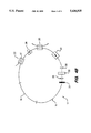
- FIG. 1 shows a CPM fiber ring laser according to the invention.
- FIG. 2 is a detailed cross section of a saturable absorber.
- FIG. 3 is a schematic detailing the focusing scheme.
- FIG. 4 including A and B, illustrates configurations used to demonstrate polarization insensitivity of the CPM configuration.
- the invention is embodied in a ring which includes a semiconductor saturable absorber (FIG. 1, 30).
- a semiconductor saturable absorber FIG. 1, 30.
- a CPM fiber ring laser is assembled so as to include a semiconductor saturable absorber (FIG. 1, 30).
- the resulting laser does not require an isolator or mirror (which lowers manufacturing costs).
- the laser is compact due to the ring configuration; it will produce sub-picosecond optical pulses with repetition rates of several tens of megahertz.
- a CPM fiber ring laser generally 12, according to the invention, includes a fiber loop 14, consisting of both single mode fiber 16 and erbium-doped amplifier fiber 18.
- the fiber loop 14 has an output coupler 20, a wavelength division multiplexer coupler 22, a filter 24, a first and second lens 26, 28 and a semiconductor saturable absorber 30.
- the filter 24 helps to stabilize the laser, but is not essential to the functioning as the laser will operate without a filter.
- lenses 26, 28 are not essential. It is apparent that FIG. 1 is not to scale.
- the CPM fiber laser works as follows. As with most lasers, the optical pulses in a CPM fiber laser are started from spontaneous emission (or noise) from the fiber amplifier. The pulses are amplified by the fiber amplifier; the saturable absorber shapes the pulses. Since the loss is minimal when the two counterpropagating pulses collide on the semiconductor saturable absorber, eventually the two counterpropagating pulses become the main lasing mode of the CPM fiber laser.
- the colliding pulse mode-locking configuration is especially useful for fiber lasers. Wrapping fiber into a ring configuration is easily done and is often preferable to a linear cavity due to the fiber's ability to confine light to a high degree.
- the colliding pulse effect enhances the pulse shaping mechanism of the saturable absorber.
- the above described components are commercially available.
- the erbium-doped fiber amplifier can be purchased from AT&T; approximately 8 meter with Er dopant concentration of 300 ppm fiber is used in the invention described herein.
- the band pass filter has a center wavelength of 1553 nm and a bandwidth of 5.0 nm is available from Omega Optical Inc.
- the wavelength division multiplexer (980 nm/1550 nm) is available from Amphenol Corp., as are output couplers (ratio 17%).
- the GRIN lenses (0.22 pitch) are available through NSG American, Inc.
- the semiconductor saturable absorber can be grown using an MOCVD machine (available from Swan, Inc.) and using substrate available from Sumitomo, Inc.
- MOCVD machine available from Swan, Inc.
- substrate available from Sumitomo, Inc.
- a 2.0 (+/-0.2) micrometer epitaxial growth of InGaAsP is desirable, with a bandgap of 1.567 micrometers (+/-.030 micrometers).
- the epitaxial growth layer may be as thick as 6 micrometers.
- An antireflection coating is applied to both side of the saturable absorber using Si x N x , at a wavelength of 1.55 micrometers.
- the antireflection coating service may be obtained commercially through Denton Vacuum, Inc.
- the CPM configuration using a semiconductor saturable absorber provides an advantage in that it is not sensitive to polarization disturbance to the fiber as discovered through experimentation. It has been found that the invention, a CPM fiber with a saturable absorber, can tolerate large amounts of polarization disturbance. Through a comparison of colliding pulse configuration with that of unidirectional ring configuration, it was found experimentally that the CPM configuration can withstand much larger polarization disturbances.
- FIG. 2 shows a cross section of a saturable absorber 30, including the active layer 34 and the substrate layer 32.
- the active layer 34 is 2.0 micrometers thick and the substrate layer 32 is 0.3 millimeters thick.
- the antireflection coating on each side 36 of the saturable absorber 30 reduces reflection to less than 1% per surface.
- the absorptive layer is comprised of a combination of materials selected form group III and IV of the Periodic Table of the Elements. Preferred combinations include InGaAsP, InPAs and InGaAs.
- the substrate provides support to the absorptive layer and preferred combinations include InP and GaAs.
- implantation dosages on a saturable absorber tends to produce a laser generating a poor quality pulse, which has pedestal.
- Lower implantation dosages on the saturable absorber tends to produce wider pulses.
- the preferred protocols are those which produce a saturable absorber capable of short, pedestal free pulses.
- FIG. 3 depicts the optimum focusing scheme of the invention with respect to the relationship of the fiber ends 15 and the saturable absorber 30.
- the fiber ends 15 are polished at an angle of approximately 10°.
- the optimal spacing between fiber end 15 and first GRIN lens 26 is represented in FIG. 3 by 42 and in the preferred embodiment, 42 has the value of 7 mm.
- the spacing between first GRIN lens 26 and the saturable absorber 30 is represented in FIG. 3 by 44 and in the preferred embodiment 44 has the value of 2 mm.
- the distance between the saturable absorber 30 and the second GRIN lens 28 is represented by 46 and in the preferred embodiment 46 has the value of 2 mm.
- the lens configuration produces a 3:1 image reduction on the saturable absorber.
- the saturable absorber directly in the optical path without using a lens. This can be accomplished by lapping down the substrate layer of semiconductor saturable absorber to less than 100 micrometers and then placing the two fiber ends in direct contact with the saturable absorber. Since the saturable absorber is so thin, efficient coupling between the two fiber ends can be achieved without using lenses.
- the colliding pulse configuration reduced the sensitivity of the mode-locked fiber laser to the polarization variation.
- the configuration depicted in FIG. 4A can tolerate large polarization variation.
- the polarization controller 38 consists of three fiber loops. Each of the fiber loops simulates a quarter wave plate. The adjustment of polarization is accomplished by changing the orientation of the fiber loop in a 0 to 180 degree range. When FIG. 4A laser is mode-locked, stable mode-locked output can be maintained when the polarization controller is in the 0 to 120 degree range.
- the FIG. 4B laser configuration can tolerate much less polarization variation.
- stable mode-locked output can be maintained only when polarization controller is varied within 5 degrees (as compared with 120 degrees in laser configuration 4A).
- the CPM (colliding pulse mode-locked) configuration tolerates much more polarization variation than a unidirectional ring configuration.
- the present invention provides a method and apparatus for generating short optical pulses on the order of 1-2 picoseconds or less, with repetition rates in the tens of megahertz, which is self-starting and polarization insensitive.
- a laser system that embodies the principles of the invention is less sensitive to polarization variation, is capable of higher repetition rates, requires fewer components and, therefore, lowers production costs. For these and other advantages provided by the invention herein, it is superior to lasers currently available in its ease of use.
Landscapes
- Physics & Mathematics (AREA)
- Electromagnetism (AREA)
- Engineering & Computer Science (AREA)
- Plasma & Fusion (AREA)
- Optics & Photonics (AREA)
- Chemical & Material Sciences (AREA)
- Materials Engineering (AREA)
- Nanotechnology (AREA)
- Lasers (AREA)
Abstract
Description
Claims (21)
Priority Applications (4)
| Application Number | Priority Date | Filing Date | Title |
|---|---|---|---|
| US08/205,671 US5436925A (en) | 1994-03-01 | 1994-03-01 | Colliding pulse mode-locked fiber ring laser using a semiconductor saturable absorber |
| DE69502642T DE69502642T2 (en) | 1994-03-01 | 1995-02-17 | Ring laser |
| EP95301031A EP0670617B1 (en) | 1994-03-01 | 1995-02-17 | Ring laser |
| JP7040593A JPH07307511A (en) | 1994-03-01 | 1995-02-28 | Fiber laser of collision pulse mode lock ring-form using semiconductor saturation possibility absorber |
Applications Claiming Priority (1)
| Application Number | Priority Date | Filing Date | Title |
|---|---|---|---|
| US08/205,671 US5436925A (en) | 1994-03-01 | 1994-03-01 | Colliding pulse mode-locked fiber ring laser using a semiconductor saturable absorber |
Publications (1)
| Publication Number | Publication Date |
|---|---|
| US5436925A true US5436925A (en) | 1995-07-25 |
Family
ID=22763164
Family Applications (1)
| Application Number | Title | Priority Date | Filing Date |
|---|---|---|---|
| US08/205,671 Expired - Fee Related US5436925A (en) | 1994-03-01 | 1994-03-01 | Colliding pulse mode-locked fiber ring laser using a semiconductor saturable absorber |
Country Status (4)
| Country | Link |
|---|---|
| US (1) | US5436925A (en) |
| EP (1) | EP0670617B1 (en) |
| JP (1) | JPH07307511A (en) |
| DE (1) | DE69502642T2 (en) |
Cited By (60)
| Publication number | Priority date | Publication date | Assignee | Title |
|---|---|---|---|---|
| US5646951A (en) * | 1994-03-24 | 1997-07-08 | Technion Research & Development Foundation Ltd. | Method and apparatus for linewidth narrowing and single mode operation in lasers by intra-cavity nonlinear wave mixing |
| US5828682A (en) * | 1996-12-13 | 1998-10-27 | Massachusetts Institute Of Technology | Rational-harmonic apparatus and technique |
| US6034975A (en) * | 1998-03-09 | 2000-03-07 | Imra America, Inc. | High power, passively modelocked fiber laser, and method of construction |
| US6072811A (en) * | 1998-02-11 | 2000-06-06 | Imra America | Integrated passively modelocked fiber lasers and method for constructing the same |
| US6097741A (en) * | 1998-02-17 | 2000-08-01 | Calmar Optcom, Inc. | Passively mode-locked fiber lasers |
| US6252892B1 (en) | 1998-09-08 | 2001-06-26 | Imra America, Inc. | Resonant fabry-perot semiconductor saturable absorbers and two photon absorption power limiters |
| US20030202547A1 (en) * | 1998-11-25 | 2003-10-30 | Fermann Martin E. | Multi-mode fiber amplifier |
| US20040161006A1 (en) * | 2003-02-18 | 2004-08-19 | Ying-Lan Chang | Method and apparatus for improving wavelength stability for InGaAsN devices |
| US20050018714A1 (en) * | 2003-07-25 | 2005-01-27 | Fermann Martin E. | Polarization maintaining dispersion controlled fiber laser source of ultrashort pulses |
| US20080001260A1 (en) * | 2006-06-29 | 2008-01-03 | International Business Machines Corporation | Mosfets comprising source/drain recesses with slanted sidewall surfaces, and methods for fabricating the same |
| US20080310859A1 (en) * | 2007-06-13 | 2008-12-18 | International Business Machines Corporation | Optical pulse amplication apparatus and method |
| DE102007057856A1 (en) | 2007-11-29 | 2009-07-02 | Toptica Photonics Ag | Fiber laser with annular resonator |
| US7602825B1 (en) | 2004-10-20 | 2009-10-13 | Calmar Optcom, Inc. | Tunable passively mode-locked lasers with phase-lock feedback for low timing jitters |
| EP2138876A1 (en) * | 2008-06-27 | 2009-12-30 | Honeywell International Inc. | Micro-optics photonic bandgap fiber coupler |
| US20100074279A1 (en) * | 1993-12-20 | 2010-03-25 | Imra America, Inc. | Environmentally stable passively modelocked fiber laser pulse source |
| US20110064096A1 (en) * | 2009-09-16 | 2011-03-17 | University Of Central Florida Research Foundation, Inc. | Mid-IR laser employing Tm fiber laser and optical parametric oscillator |
| CN102074880A (en) * | 2010-12-20 | 2011-05-25 | 北京交通大学 | Single-mode fiber laser with mini resonance cavity structure |
| US8208196B2 (en) | 2003-07-25 | 2012-06-26 | Imra America, Inc. | Pulsed laser sources |
| US20130330080A1 (en) * | 2012-06-06 | 2013-12-12 | Innolight Technology (Suzhou) Ltd. | Wavelength Division Multiplexing/De-Multiplexing Optical Assembly for High Speed Parallel Long Distance Transmission |
| US9071037B2 (en) * | 2004-03-31 | 2015-06-30 | Imra America, Inc. | High power short pulse fiber laser |
| US9517963B2 (en) | 2013-12-17 | 2016-12-13 | Corning Incorporated | Method for rapid laser drilling of holes in glass and products made therefrom |
| US9617180B2 (en) | 2014-07-14 | 2017-04-11 | Corning Incorporated | Methods and apparatuses for fabricating glass articles |
| US9676167B2 (en) | 2013-12-17 | 2017-06-13 | Corning Incorporated | Laser processing of sapphire substrate and related applications |
| US9687936B2 (en) | 2013-12-17 | 2017-06-27 | Corning Incorporated | Transparent material cutting with ultrafast laser and beam optics |
| US20170189991A1 (en) * | 2014-07-14 | 2017-07-06 | Corning Incorporated | Systems and methods for processing transparent materials using adjustable laser beam focal lines |
| US9701564B2 (en) | 2013-01-15 | 2017-07-11 | Corning Incorporated | Systems and methods of glass cutting by inducing pulsed laser perforations into glass articles |
| US9701563B2 (en) | 2013-12-17 | 2017-07-11 | Corning Incorporated | Laser cut composite glass article and method of cutting |
| CN107248692A (en) * | 2017-05-19 | 2017-10-13 | 武汉理工大学 | A kind of compound cavity optical fibre laser of super-narrow line width Wavelength tunable |
| EP2557641A4 (en) * | 2010-04-09 | 2017-11-01 | Hamamatsu Photonics K.K. | Pulse fiber laser device |
| US9815730B2 (en) | 2013-12-17 | 2017-11-14 | Corning Incorporated | Processing 3D shaped transparent brittle substrate |
| US9815144B2 (en) | 2014-07-08 | 2017-11-14 | Corning Incorporated | Methods and apparatuses for laser processing materials |
| WO2017212098A1 (en) * | 2016-06-06 | 2017-12-14 | Universidad de Alcalá de Henares | Mode-locked pulsed laser comprising a saturable absorber |
| US9850159B2 (en) | 2012-11-20 | 2017-12-26 | Corning Incorporated | High speed laser processing of transparent materials |
| US9850160B2 (en) | 2013-12-17 | 2017-12-26 | Corning Incorporated | Laser cutting of display glass compositions |
| US10047001B2 (en) | 2014-12-04 | 2018-08-14 | Corning Incorporated | Glass cutting systems and methods using non-diffracting laser beams |
| US10173916B2 (en) | 2013-12-17 | 2019-01-08 | Corning Incorporated | Edge chamfering by mechanically processing laser cut glass |
| US10233112B2 (en) | 2013-12-17 | 2019-03-19 | Corning Incorporated | Laser processing of slots and holes |
| US10252931B2 (en) | 2015-01-12 | 2019-04-09 | Corning Incorporated | Laser cutting of thermally tempered substrates |
| US10280108B2 (en) | 2013-03-21 | 2019-05-07 | Corning Laser Technologies GmbH | Device and method for cutting out contours from planar substrates by means of laser |
| US10335902B2 (en) | 2014-07-14 | 2019-07-02 | Corning Incorporated | Method and system for arresting crack propagation |
| US10377658B2 (en) | 2016-07-29 | 2019-08-13 | Corning Incorporated | Apparatuses and methods for laser processing |
| US10421683B2 (en) | 2013-01-15 | 2019-09-24 | Corning Laser Technologies GmbH | Method and device for the laser-based machining of sheet-like substrates |
| US10522963B2 (en) | 2016-08-30 | 2019-12-31 | Corning Incorporated | Laser cutting of materials with intensity mapping optical system |
| US10525657B2 (en) | 2015-03-27 | 2020-01-07 | Corning Incorporated | Gas permeable window and method of fabricating the same |
| US10526234B2 (en) | 2014-07-14 | 2020-01-07 | Corning Incorporated | Interface block; system for and method of cutting a substrate being transparent within a range of wavelengths using such interface block |
| US10611667B2 (en) | 2014-07-14 | 2020-04-07 | Corning Incorporated | Method and system for forming perforations |
| US10626040B2 (en) | 2017-06-15 | 2020-04-21 | Corning Incorporated | Articles capable of individual singulation |
| US10688599B2 (en) | 2017-02-09 | 2020-06-23 | Corning Incorporated | Apparatus and methods for laser processing transparent workpieces using phase shifted focal lines |
| US10730783B2 (en) | 2016-09-30 | 2020-08-04 | Corning Incorporated | Apparatuses and methods for laser processing transparent workpieces using non-axisymmetric beam spots |
| US10752534B2 (en) | 2016-11-01 | 2020-08-25 | Corning Incorporated | Apparatuses and methods for laser processing laminate workpiece stacks |
| US11062986B2 (en) | 2017-05-25 | 2021-07-13 | Corning Incorporated | Articles having vias with geometry attributes and methods for fabricating the same |
| US11078112B2 (en) | 2017-05-25 | 2021-08-03 | Corning Incorporated | Silica-containing substrates with vias having an axially variable sidewall taper and methods for forming the same |
| US11111170B2 (en) | 2016-05-06 | 2021-09-07 | Corning Incorporated | Laser cutting and removal of contoured shapes from transparent substrates |
| US11114309B2 (en) | 2016-06-01 | 2021-09-07 | Corning Incorporated | Articles and methods of forming vias in substrates |
| US11186060B2 (en) | 2015-07-10 | 2021-11-30 | Corning Incorporated | Methods of continuous fabrication of holes in flexible substrate sheets and products relating to the same |
| US11542190B2 (en) | 2016-10-24 | 2023-01-03 | Corning Incorporated | Substrate processing station for laser-based machining of sheet-like glass substrates |
| US11554984B2 (en) | 2018-02-22 | 2023-01-17 | Corning Incorporated | Alkali-free borosilicate glasses with low post-HF etch roughness |
| US11556039B2 (en) | 2013-12-17 | 2023-01-17 | Corning Incorporated | Electrochromic coated glass articles and methods for laser processing the same |
| US11774233B2 (en) | 2016-06-29 | 2023-10-03 | Corning Incorporated | Method and system for measuring geometric parameters of through holes |
| US11773004B2 (en) | 2015-03-24 | 2023-10-03 | Corning Incorporated | Laser cutting and processing of display glass compositions |
Families Citing this family (4)
| Publication number | Priority date | Publication date | Assignee | Title |
|---|---|---|---|---|
| FI121040B (en) * | 2005-05-10 | 2010-06-15 | Reflekron Oy | Unlocked fiber laser |
| DE102007022561B4 (en) * | 2007-05-14 | 2010-09-16 | Meos Ag | Active rotation sensor |
| JP5675219B2 (en) * | 2010-08-27 | 2015-02-25 | キヤノン株式会社 | Optical pulse generator, terahertz spectrometer and tomography device |
| DE102014114733B4 (en) * | 2014-10-10 | 2016-11-24 | Trumpf Laser Gmbh | METHOD OF MANUFACTURING A SATURATIBLE SEMICONDUCTOR ABSORBER ELEMENT AND SATURATED SEMICONDUCTOR ABSORBER ELEMENT |
Citations (6)
| Publication number | Priority date | Publication date | Assignee | Title |
|---|---|---|---|---|
| US4504950A (en) * | 1982-03-02 | 1985-03-12 | California Institute Of Technology | Tunable graded rod laser assembly |
| US5056096A (en) * | 1989-09-20 | 1991-10-08 | Stc Plc | Hybrid doped fiber-semiconductor amplifier ring laser source |
| US5237577A (en) * | 1991-11-06 | 1993-08-17 | At&T Bell Laboratories | Monolithically integrated fabry-perot saturable absorber |
| US5251230A (en) * | 1992-05-08 | 1993-10-05 | Honeywell, Inc. | Resonant cavity dither with index of refraction modulator |
| US5276701A (en) * | 1992-09-18 | 1994-01-04 | Fujitsu Limited | Ring laser employing unidirectional attenuator |
| US5278855A (en) * | 1992-05-11 | 1994-01-11 | At&T Bell Laboratories | Broadband semiconductor saturable absorber |
-
1994
- 1994-03-01 US US08/205,671 patent/US5436925A/en not_active Expired - Fee Related
-
1995
- 1995-02-17 DE DE69502642T patent/DE69502642T2/en not_active Expired - Fee Related
- 1995-02-17 EP EP95301031A patent/EP0670617B1/en not_active Expired - Lifetime
- 1995-02-28 JP JP7040593A patent/JPH07307511A/en active Pending
Patent Citations (6)
| Publication number | Priority date | Publication date | Assignee | Title |
|---|---|---|---|---|
| US4504950A (en) * | 1982-03-02 | 1985-03-12 | California Institute Of Technology | Tunable graded rod laser assembly |
| US5056096A (en) * | 1989-09-20 | 1991-10-08 | Stc Plc | Hybrid doped fiber-semiconductor amplifier ring laser source |
| US5237577A (en) * | 1991-11-06 | 1993-08-17 | At&T Bell Laboratories | Monolithically integrated fabry-perot saturable absorber |
| US5251230A (en) * | 1992-05-08 | 1993-10-05 | Honeywell, Inc. | Resonant cavity dither with index of refraction modulator |
| US5278855A (en) * | 1992-05-11 | 1994-01-11 | At&T Bell Laboratories | Broadband semiconductor saturable absorber |
| US5276701A (en) * | 1992-09-18 | 1994-01-04 | Fujitsu Limited | Ring laser employing unidirectional attenuator |
Cited By (106)
| Publication number | Priority date | Publication date | Assignee | Title |
|---|---|---|---|---|
| US8130799B2 (en) | 1993-12-20 | 2012-03-06 | Imra America, Inc. | Environmentally stable passively modelocked fiber laser pulse source |
| US20100074279A1 (en) * | 1993-12-20 | 2010-03-25 | Imra America, Inc. | Environmentally stable passively modelocked fiber laser pulse source |
| US8548014B2 (en) | 1993-12-20 | 2013-10-01 | Imra America, Inc. | Environmentally stable passively modelocked fiber laser pulse source |
| US5646951A (en) * | 1994-03-24 | 1997-07-08 | Technion Research & Development Foundation Ltd. | Method and apparatus for linewidth narrowing and single mode operation in lasers by intra-cavity nonlinear wave mixing |
| US5828682A (en) * | 1996-12-13 | 1998-10-27 | Massachusetts Institute Of Technology | Rational-harmonic apparatus and technique |
| US6373867B1 (en) | 1997-07-11 | 2002-04-16 | Calmar Optcom, Inc. | Generation of a wavelength-tunable laser oscillation in a wave-guiding gain medium based on passive mode lock |
| US6570892B1 (en) | 1997-07-11 | 2003-05-27 | Calmar Optcom, Inc. | Passively mode-locked fiber lasers |
| US6072811A (en) * | 1998-02-11 | 2000-06-06 | Imra America | Integrated passively modelocked fiber lasers and method for constructing the same |
| US6097741A (en) * | 1998-02-17 | 2000-08-01 | Calmar Optcom, Inc. | Passively mode-locked fiber lasers |
| US6034975A (en) * | 1998-03-09 | 2000-03-07 | Imra America, Inc. | High power, passively modelocked fiber laser, and method of construction |
| US20050286569A1 (en) * | 1998-09-08 | 2005-12-29 | Min Jiang | Resonant fabry-perot semiconductor saturable absorbers and two photon absorption power limiters |
| US6252892B1 (en) | 1998-09-08 | 2001-06-26 | Imra America, Inc. | Resonant fabry-perot semiconductor saturable absorbers and two photon absorption power limiters |
| US6956887B2 (en) | 1998-09-08 | 2005-10-18 | Imra America, Inc. | Resonant fabry-perot semiconductor saturable absorbers and two photon absorption power limiters |
| US6819694B2 (en) | 1998-09-08 | 2004-11-16 | Imra America, Inc. | Resonant fabry-perot semiconductor saturable absorbers and two photon absorption power limiters |
| US7453913B2 (en) | 1998-09-08 | 2008-11-18 | Imra America, Inc. | Resonant Fabry-Perot semiconductor saturable absorbers and two photon absorption power limiters |
| US8761211B2 (en) * | 1998-11-25 | 2014-06-24 | Imra America, Inc. | Multi-mode fiber amplifier |
| US20050008044A1 (en) * | 1998-11-25 | 2005-01-13 | Fermann Martin E. | Mode-locked multi-mode fiber laser pulse source |
| US20030202547A1 (en) * | 1998-11-25 | 2003-10-30 | Fermann Martin E. | Multi-mode fiber amplifier |
| US9595802B2 (en) | 1998-11-25 | 2017-03-14 | Imra America, Inc. | Multi-mode fiber amplifier |
| US9570880B2 (en) | 1998-11-25 | 2017-02-14 | Imra America, Inc. | Multi-mode fiber amplifier |
| US20040161006A1 (en) * | 2003-02-18 | 2004-08-19 | Ying-Lan Chang | Method and apparatus for improving wavelength stability for InGaAsN devices |
| US7088756B2 (en) | 2003-07-25 | 2006-08-08 | Imra America, Inc. | Polarization maintaining dispersion controlled fiber laser source of ultrashort pulses |
| US9401579B2 (en) | 2003-07-25 | 2016-07-26 | Imra America, Inc. | Pulsed laser sources |
| US8599473B2 (en) | 2003-07-25 | 2013-12-03 | Imra America, Inc. | Pulsed laser sources |
| US9653868B2 (en) | 2003-07-25 | 2017-05-16 | Imra America, Inc. | Pulsed laser sources |
| US8456735B2 (en) | 2003-07-25 | 2013-06-04 | Imra America, Inc. | Pulsed laser sources |
| US20050018714A1 (en) * | 2003-07-25 | 2005-01-27 | Fermann Martin E. | Polarization maintaining dispersion controlled fiber laser source of ultrashort pulses |
| US8208196B2 (en) | 2003-07-25 | 2012-06-26 | Imra America, Inc. | Pulsed laser sources |
| US9071037B2 (en) * | 2004-03-31 | 2015-06-30 | Imra America, Inc. | High power short pulse fiber laser |
| US9640940B2 (en) | 2004-03-31 | 2017-05-02 | Imra America, Inc. | High power short pulse fiber laser |
| US7602825B1 (en) | 2004-10-20 | 2009-10-13 | Calmar Optcom, Inc. | Tunable passively mode-locked lasers with phase-lock feedback for low timing jitters |
| US20080001260A1 (en) * | 2006-06-29 | 2008-01-03 | International Business Machines Corporation | Mosfets comprising source/drain recesses with slanted sidewall surfaces, and methods for fabricating the same |
| US20080057710A1 (en) * | 2006-06-29 | 2008-03-06 | International Business Machines Corporation | Mosfets comprising source/drain recesses with slanted sidewall surfaces, and methods for fabricating the same |
| US7816261B2 (en) | 2006-06-29 | 2010-10-19 | International Business Machines Corporation | MOSFETS comprising source/drain recesses with slanted sidewall surfaces, and methods for fabricating the same |
| US7560758B2 (en) | 2006-06-29 | 2009-07-14 | International Business Machines Corporation | MOSFETs comprising source/drain recesses with slanted sidewall surfaces, and methods for fabricating the same |
| US8036537B2 (en) * | 2007-06-13 | 2011-10-11 | International Business Machines Corporation | Optical pulse amplication apparatus and method |
| US8233807B2 (en) | 2007-06-13 | 2012-07-31 | International Business Machines Corporation | Optical pulse amplication apparatus and method |
| US20080310859A1 (en) * | 2007-06-13 | 2008-12-18 | International Business Machines Corporation | Optical pulse amplication apparatus and method |
| US8457164B2 (en) | 2007-11-29 | 2013-06-04 | Toptica Photonics Ag | Fiber laser comprising a ring-shaped resonator |
| DE102007057856B4 (en) * | 2007-11-29 | 2017-08-10 | Toptica Photonics Ag | Fiber laser with annular resonator |
| US20100296528A1 (en) * | 2007-11-29 | 2010-11-25 | Toptica Photonics Ag | Fiber laser comprising a ring-shaped resonator |
| DE102007057856A1 (en) | 2007-11-29 | 2009-07-02 | Toptica Photonics Ag | Fiber laser with annular resonator |
| US20090324169A1 (en) * | 2008-06-27 | 2009-12-31 | Honeywell International Inc. | Micro-optics photonic bandgap fiber coupler |
| US7680372B2 (en) | 2008-06-27 | 2010-03-16 | Honeywell International Inc. | Micro-optics photonic bandgap fiber coupler |
| EP2138876A1 (en) * | 2008-06-27 | 2009-12-30 | Honeywell International Inc. | Micro-optics photonic bandgap fiber coupler |
| US20110064096A1 (en) * | 2009-09-16 | 2011-03-17 | University Of Central Florida Research Foundation, Inc. | Mid-IR laser employing Tm fiber laser and optical parametric oscillator |
| EP2557641A4 (en) * | 2010-04-09 | 2017-11-01 | Hamamatsu Photonics K.K. | Pulse fiber laser device |
| CN102074880A (en) * | 2010-12-20 | 2011-05-25 | 北京交通大学 | Single-mode fiber laser with mini resonance cavity structure |
| US20130330080A1 (en) * | 2012-06-06 | 2013-12-12 | Innolight Technology (Suzhou) Ltd. | Wavelength Division Multiplexing/De-Multiplexing Optical Assembly for High Speed Parallel Long Distance Transmission |
| US9850159B2 (en) | 2012-11-20 | 2017-12-26 | Corning Incorporated | High speed laser processing of transparent materials |
| US11345625B2 (en) | 2013-01-15 | 2022-05-31 | Corning Laser Technologies GmbH | Method and device for the laser-based machining of sheet-like substrates |
| US11028003B2 (en) | 2013-01-15 | 2021-06-08 | Corning Laser Technologies GmbH | Method and device for laser-based machining of flat substrates |
| US10421683B2 (en) | 2013-01-15 | 2019-09-24 | Corning Laser Technologies GmbH | Method and device for the laser-based machining of sheet-like substrates |
| US9701564B2 (en) | 2013-01-15 | 2017-07-11 | Corning Incorporated | Systems and methods of glass cutting by inducing pulsed laser perforations into glass articles |
| US11713271B2 (en) | 2013-03-21 | 2023-08-01 | Corning Laser Technologies GmbH | Device and method for cutting out contours from planar substrates by means of laser |
| US10280108B2 (en) | 2013-03-21 | 2019-05-07 | Corning Laser Technologies GmbH | Device and method for cutting out contours from planar substrates by means of laser |
| US9701563B2 (en) | 2013-12-17 | 2017-07-11 | Corning Incorporated | Laser cut composite glass article and method of cutting |
| US10293436B2 (en) | 2013-12-17 | 2019-05-21 | Corning Incorporated | Method for rapid laser drilling of holes in glass and products made therefrom |
| US9676167B2 (en) | 2013-12-17 | 2017-06-13 | Corning Incorporated | Laser processing of sapphire substrate and related applications |
| US9517963B2 (en) | 2013-12-17 | 2016-12-13 | Corning Incorporated | Method for rapid laser drilling of holes in glass and products made therefrom |
| US11148225B2 (en) | 2013-12-17 | 2021-10-19 | Corning Incorporated | Method for rapid laser drilling of holes in glass and products made therefrom |
| US9850160B2 (en) | 2013-12-17 | 2017-12-26 | Corning Incorporated | Laser cutting of display glass compositions |
| US10611668B2 (en) | 2013-12-17 | 2020-04-07 | Corning Incorporated | Laser cut composite glass article and method of cutting |
| US10597321B2 (en) | 2013-12-17 | 2020-03-24 | Corning Incorporated | Edge chamfering methods |
| US10144093B2 (en) | 2013-12-17 | 2018-12-04 | Corning Incorporated | Method for rapid laser drilling of holes in glass and products made therefrom |
| US10173916B2 (en) | 2013-12-17 | 2019-01-08 | Corning Incorporated | Edge chamfering by mechanically processing laser cut glass |
| US10179748B2 (en) | 2013-12-17 | 2019-01-15 | Corning Incorporated | Laser processing of sapphire substrate and related applications |
| US10183885B2 (en) | 2013-12-17 | 2019-01-22 | Corning Incorporated | Laser cut composite glass article and method of cutting |
| US10233112B2 (en) | 2013-12-17 | 2019-03-19 | Corning Incorporated | Laser processing of slots and holes |
| US9815730B2 (en) | 2013-12-17 | 2017-11-14 | Corning Incorporated | Processing 3D shaped transparent brittle substrate |
| US11556039B2 (en) | 2013-12-17 | 2023-01-17 | Corning Incorporated | Electrochromic coated glass articles and methods for laser processing the same |
| US10442719B2 (en) | 2013-12-17 | 2019-10-15 | Corning Incorporated | Edge chamfering methods |
| US9687936B2 (en) | 2013-12-17 | 2017-06-27 | Corning Incorporated | Transparent material cutting with ultrafast laser and beam optics |
| US10392290B2 (en) | 2013-12-17 | 2019-08-27 | Corning Incorporated | Processing 3D shaped transparent brittle substrate |
| US11697178B2 (en) | 2014-07-08 | 2023-07-11 | Corning Incorporated | Methods and apparatuses for laser processing materials |
| US9815144B2 (en) | 2014-07-08 | 2017-11-14 | Corning Incorporated | Methods and apparatuses for laser processing materials |
| US11648623B2 (en) * | 2014-07-14 | 2023-05-16 | Corning Incorporated | Systems and methods for processing transparent materials using adjustable laser beam focal lines |
| US10335902B2 (en) | 2014-07-14 | 2019-07-02 | Corning Incorporated | Method and system for arresting crack propagation |
| US20170189991A1 (en) * | 2014-07-14 | 2017-07-06 | Corning Incorporated | Systems and methods for processing transparent materials using adjustable laser beam focal lines |
| US9617180B2 (en) | 2014-07-14 | 2017-04-11 | Corning Incorporated | Methods and apparatuses for fabricating glass articles |
| US10526234B2 (en) | 2014-07-14 | 2020-01-07 | Corning Incorporated | Interface block; system for and method of cutting a substrate being transparent within a range of wavelengths using such interface block |
| US10611667B2 (en) | 2014-07-14 | 2020-04-07 | Corning Incorporated | Method and system for forming perforations |
| US9975799B2 (en) | 2014-07-14 | 2018-05-22 | Corning Incorporated | Methods and apparatuses for fabricating glass articles |
| US11014845B2 (en) | 2014-12-04 | 2021-05-25 | Corning Incorporated | Method of laser cutting glass using non-diffracting laser beams |
| US10047001B2 (en) | 2014-12-04 | 2018-08-14 | Corning Incorporated | Glass cutting systems and methods using non-diffracting laser beams |
| US10252931B2 (en) | 2015-01-12 | 2019-04-09 | Corning Incorporated | Laser cutting of thermally tempered substrates |
| US11773004B2 (en) | 2015-03-24 | 2023-10-03 | Corning Incorporated | Laser cutting and processing of display glass compositions |
| US10525657B2 (en) | 2015-03-27 | 2020-01-07 | Corning Incorporated | Gas permeable window and method of fabricating the same |
| US11186060B2 (en) | 2015-07-10 | 2021-11-30 | Corning Incorporated | Methods of continuous fabrication of holes in flexible substrate sheets and products relating to the same |
| US11111170B2 (en) | 2016-05-06 | 2021-09-07 | Corning Incorporated | Laser cutting and removal of contoured shapes from transparent substrates |
| US11114309B2 (en) | 2016-06-01 | 2021-09-07 | Corning Incorporated | Articles and methods of forming vias in substrates |
| WO2017212098A1 (en) * | 2016-06-06 | 2017-12-14 | Universidad de Alcalá de Henares | Mode-locked pulsed laser comprising a saturable absorber |
| US11774233B2 (en) | 2016-06-29 | 2023-10-03 | Corning Incorporated | Method and system for measuring geometric parameters of through holes |
| US10377658B2 (en) | 2016-07-29 | 2019-08-13 | Corning Incorporated | Apparatuses and methods for laser processing |
| US10522963B2 (en) | 2016-08-30 | 2019-12-31 | Corning Incorporated | Laser cutting of materials with intensity mapping optical system |
| US11130701B2 (en) | 2016-09-30 | 2021-09-28 | Corning Incorporated | Apparatuses and methods for laser processing transparent workpieces using non-axisymmetric beam spots |
| US10730783B2 (en) | 2016-09-30 | 2020-08-04 | Corning Incorporated | Apparatuses and methods for laser processing transparent workpieces using non-axisymmetric beam spots |
| US11542190B2 (en) | 2016-10-24 | 2023-01-03 | Corning Incorporated | Substrate processing station for laser-based machining of sheet-like glass substrates |
| US10752534B2 (en) | 2016-11-01 | 2020-08-25 | Corning Incorporated | Apparatuses and methods for laser processing laminate workpiece stacks |
| US10688599B2 (en) | 2017-02-09 | 2020-06-23 | Corning Incorporated | Apparatus and methods for laser processing transparent workpieces using phase shifted focal lines |
| CN107248692A (en) * | 2017-05-19 | 2017-10-13 | 武汉理工大学 | A kind of compound cavity optical fibre laser of super-narrow line width Wavelength tunable |
| US11972993B2 (en) | 2017-05-25 | 2024-04-30 | Corning Incorporated | Silica-containing substrates with vias having an axially variable sidewall taper and methods for forming the same |
| US11062986B2 (en) | 2017-05-25 | 2021-07-13 | Corning Incorporated | Articles having vias with geometry attributes and methods for fabricating the same |
| US11078112B2 (en) | 2017-05-25 | 2021-08-03 | Corning Incorporated | Silica-containing substrates with vias having an axially variable sidewall taper and methods for forming the same |
| US10626040B2 (en) | 2017-06-15 | 2020-04-21 | Corning Incorporated | Articles capable of individual singulation |
| US11554984B2 (en) | 2018-02-22 | 2023-01-17 | Corning Incorporated | Alkali-free borosilicate glasses with low post-HF etch roughness |
Also Published As
| Publication number | Publication date |
|---|---|
| DE69502642T2 (en) | 1998-09-17 |
| EP0670617A1 (en) | 1995-09-06 |
| JPH07307511A (en) | 1995-11-21 |
| DE69502642D1 (en) | 1998-07-02 |
| EP0670617B1 (en) | 1998-05-27 |
Similar Documents
| Publication | Publication Date | Title |
|---|---|---|
| US5436925A (en) | Colliding pulse mode-locked fiber ring laser using a semiconductor saturable absorber | |
| Taccheo et al. | Diode-pumped bulk erbium-ytterbium lasers | |
| FI113719B (en) | modulator | |
| US20100284430A1 (en) | Systems and methods for generating high repetition rate ultra-short optical pulses | |
| JPH0864893A (en) | Passive harmonic divided mode-locked laser | |
| US6356693B1 (en) | Semiconductor optical pulse compression waveguide | |
| Takara et al. | 20 GHz transform-limited optical pulse generation and bit-error-free operation using a tunable, actively modelocked Er-doped fibre ring laser | |
| Arnold et al. | Modulation behavior of semiconductor injection lasers | |
| JPS5857774A (en) | Semiconductor laser | |
| FI113503B (en) | Procedure for organizing a mode-locked pulse queue by pump modulation | |
| Vawter et al. | All optical millimeter-wave electrical signal generation using an integrated mode-locked semiconductor ring laser and photodiode | |
| US6788715B1 (en) | Stabilized laser using multiphoton absorption to reduce intensity fluctuations | |
| US3492599A (en) | Mode-locked laser pulse generator | |
| Pollock et al. | Recent progress in color center lasers | |
| Wong et al. | Introduction to lasers and optical amplifiers | |
| Russer et al. | Direct modulation of semiconductor injection lasers | |
| Imajuku et al. | Optical phase-sensitive amplification using two phase-locked light sources | |
| Lin et al. | Colliding-pulse mode-locked lasers using Er-doped fiber and a semiconductor saturable absorber | |
| Gray et al. | Passive harmonically modelocked fiber soliton laser with repetition rate above 2 GHz | |
| Yao et al. | Coupled opto-electronic oscillators | |
| Budz et al. | Ultrashort Pulse Amplification at 1080 nm With a Long-Wavelength InGaAs–GaAs Flared Amplifier | |
| Murata et al. | 1.5¿ um Wavelength Tunable DBR Lasers with Large Continuous Tuning Ranges and Narrow Spectral Linewidths | |
| Pribil et al. | 4 Laser Transmitters | |
| Guina et al. | Mode-locked fiber lasers based on semiconductor saturable absorbers | |
| Lourtioz et al. | Ultrashort Tunable Emission from Gain-/Q-Switched Laser Diodes with Highly Attenuating Selective External Cavity |
Legal Events
| Date | Code | Title | Description |
|---|---|---|---|
| AS | Assignment |
Owner name: HEWLETT-PACKARD COMPANY, CALIFORNIA Free format text: ASSIGNMENT OF ASSIGNORS INTEREST;ASSIGNORS:LIN, HONG;CHANG, KOK-WAI;DONALD, DAVID K.;REEL/FRAME:006945/0054 Effective date: 19940301 |
|
| FEPP | Fee payment procedure |
Free format text: PAYOR NUMBER ASSIGNED (ORIGINAL EVENT CODE: ASPN); ENTITY STATUS OF PATENT OWNER: LARGE ENTITY |
|
| FPAY | Fee payment |
Year of fee payment: 4 |
|
| AS | Assignment |
Owner name: HEWLETT-PACKARD COMPANY, A DELAWARE CORPORATION, C Free format text: MERGER;ASSIGNOR:HEWLETT-PACKARD COMPANY, A CALIFORNIA CORPORATION;REEL/FRAME:010841/0649 Effective date: 19980520 |
|
| AS | Assignment |
Owner name: AGILENT TECHNOLOGIES INC, CALIFORNIA Free format text: ASSIGNMENT OF ASSIGNORS INTEREST;ASSIGNOR:HEWLETT-PACKARD COMPANY;REEL/FRAME:010977/0540 Effective date: 19991101 |
|
| FPAY | Fee payment |
Year of fee payment: 8 |
|
| REMI | Maintenance fee reminder mailed | ||
| LAPS | Lapse for failure to pay maintenance fees | ||
| STCH | Information on status: patent discontinuation |
Free format text: PATENT EXPIRED DUE TO NONPAYMENT OF MAINTENANCE FEES UNDER 37 CFR 1.362 |
|
| FP | Lapsed due to failure to pay maintenance fee |
Effective date: 20070725 |