US10173916B2 - Edge chamfering by mechanically processing laser cut glass - Google Patents
Edge chamfering by mechanically processing laser cut glass Download PDFInfo
- Publication number
- US10173916B2 US10173916B2 US15/114,243 US201515114243A US10173916B2 US 10173916 B2 US10173916 B2 US 10173916B2 US 201515114243 A US201515114243 A US 201515114243A US 10173916 B2 US10173916 B2 US 10173916B2
- Authority
- US
- United States
- Prior art keywords
- laser
- workpiece
- edge
- laser beam
- wheel
- Prior art date
- Legal status (The legal status is an assumption and is not a legal conclusion. Google has not performed a legal analysis and makes no representation as to the accuracy of the status listed.)
- Expired - Fee Related
Links
- 0 C(C1)*C2C1=C2 Chemical compound C(C1)*C2C1=C2 0.000 description 2
Images


Classifications
-
- C—CHEMISTRY; METALLURGY
- C03—GLASS; MINERAL OR SLAG WOOL
- C03B—MANUFACTURE, SHAPING, OR SUPPLEMENTARY PROCESSES
- C03B33/00—Severing cooled glass
- C03B33/02—Cutting or splitting sheet glass or ribbons; Apparatus or machines therefor
- C03B33/0222—Scoring using a focussed radiation beam, e.g. laser
-
- B—PERFORMING OPERATIONS; TRANSPORTING
- B23—MACHINE TOOLS; METAL-WORKING NOT OTHERWISE PROVIDED FOR
- B23K—SOLDERING OR UNSOLDERING; WELDING; CLADDING OR PLATING BY SOLDERING OR WELDING; CUTTING BY APPLYING HEAT LOCALLY, e.g. FLAME CUTTING; WORKING BY LASER BEAM
- B23K26/00—Working by laser beam, e.g. welding, cutting or boring
- B23K26/02—Positioning or observing the workpiece, e.g. with respect to the point of impact; Aligning, aiming or focusing the laser beam
- B23K26/035—Aligning the laser beam
- B23K26/037—Aligning the laser beam by pressing on the workpiece, e.g. pressing roller foot
-
- B—PERFORMING OPERATIONS; TRANSPORTING
- B23—MACHINE TOOLS; METAL-WORKING NOT OTHERWISE PROVIDED FOR
- B23K—SOLDERING OR UNSOLDERING; WELDING; CLADDING OR PLATING BY SOLDERING OR WELDING; CUTTING BY APPLYING HEAT LOCALLY, e.g. FLAME CUTTING; WORKING BY LASER BEAM
- B23K26/00—Working by laser beam, e.g. welding, cutting or boring
- B23K26/02—Positioning or observing the workpiece, e.g. with respect to the point of impact; Aligning, aiming or focusing the laser beam
- B23K26/04—Automatically aligning, aiming or focusing the laser beam, e.g. using the back-scattered light
-
- B—PERFORMING OPERATIONS; TRANSPORTING
- B23—MACHINE TOOLS; METAL-WORKING NOT OTHERWISE PROVIDED FOR
- B23K—SOLDERING OR UNSOLDERING; WELDING; CLADDING OR PLATING BY SOLDERING OR WELDING; CUTTING BY APPLYING HEAT LOCALLY, e.g. FLAME CUTTING; WORKING BY LASER BEAM
- B23K26/00—Working by laser beam, e.g. welding, cutting or boring
- B23K26/02—Positioning or observing the workpiece, e.g. with respect to the point of impact; Aligning, aiming or focusing the laser beam
- B23K26/06—Shaping the laser beam, e.g. by masks or multi-focusing
- B23K26/062—Shaping the laser beam, e.g. by masks or multi-focusing by direct control of the laser beam
- B23K26/0622—Shaping the laser beam, e.g. by masks or multi-focusing by direct control of the laser beam by shaping pulses
- B23K26/0624—Shaping the laser beam, e.g. by masks or multi-focusing by direct control of the laser beam by shaping pulses using ultrashort pulses, i.e. pulses of 1ns or less
-
- B—PERFORMING OPERATIONS; TRANSPORTING
- B23—MACHINE TOOLS; METAL-WORKING NOT OTHERWISE PROVIDED FOR
- B23K—SOLDERING OR UNSOLDERING; WELDING; CLADDING OR PLATING BY SOLDERING OR WELDING; CUTTING BY APPLYING HEAT LOCALLY, e.g. FLAME CUTTING; WORKING BY LASER BEAM
- B23K26/00—Working by laser beam, e.g. welding, cutting or boring
- B23K26/08—Devices involving relative movement between laser beam and workpiece
- B23K26/083—Devices involving movement of the workpiece in at least one axial direction
-
- B—PERFORMING OPERATIONS; TRANSPORTING
- B23—MACHINE TOOLS; METAL-WORKING NOT OTHERWISE PROVIDED FOR
- B23K—SOLDERING OR UNSOLDERING; WELDING; CLADDING OR PLATING BY SOLDERING OR WELDING; CUTTING BY APPLYING HEAT LOCALLY, e.g. FLAME CUTTING; WORKING BY LASER BEAM
- B23K26/00—Working by laser beam, e.g. welding, cutting or boring
- B23K26/08—Devices involving relative movement between laser beam and workpiece
- B23K26/0869—Devices involving movement of the laser head in at least one axial direction
-
- B—PERFORMING OPERATIONS; TRANSPORTING
- B23—MACHINE TOOLS; METAL-WORKING NOT OTHERWISE PROVIDED FOR
- B23K—SOLDERING OR UNSOLDERING; WELDING; CLADDING OR PLATING BY SOLDERING OR WELDING; CUTTING BY APPLYING HEAT LOCALLY, e.g. FLAME CUTTING; WORKING BY LASER BEAM
- B23K26/00—Working by laser beam, e.g. welding, cutting or boring
- B23K26/36—Removing material
- B23K26/361—Removing material for deburring or mechanical trimming
-
- B—PERFORMING OPERATIONS; TRANSPORTING
- B23—MACHINE TOOLS; METAL-WORKING NOT OTHERWISE PROVIDED FOR
- B23K—SOLDERING OR UNSOLDERING; WELDING; CLADDING OR PLATING BY SOLDERING OR WELDING; CUTTING BY APPLYING HEAT LOCALLY, e.g. FLAME CUTTING; WORKING BY LASER BEAM
- B23K26/00—Working by laser beam, e.g. welding, cutting or boring
- B23K26/36—Removing material
- B23K26/362—Laser etching
-
- B—PERFORMING OPERATIONS; TRANSPORTING
- B23—MACHINE TOOLS; METAL-WORKING NOT OTHERWISE PROVIDED FOR
- B23K—SOLDERING OR UNSOLDERING; WELDING; CLADDING OR PLATING BY SOLDERING OR WELDING; CUTTING BY APPLYING HEAT LOCALLY, e.g. FLAME CUTTING; WORKING BY LASER BEAM
- B23K26/00—Working by laser beam, e.g. welding, cutting or boring
- B23K26/36—Removing material
- B23K26/40—Removing material taking account of the properties of the material involved
- B23K26/402—Removing material taking account of the properties of the material involved involving non-metallic material, e.g. isolators
-
- B—PERFORMING OPERATIONS; TRANSPORTING
- B23—MACHINE TOOLS; METAL-WORKING NOT OTHERWISE PROVIDED FOR
- B23K—SOLDERING OR UNSOLDERING; WELDING; CLADDING OR PLATING BY SOLDERING OR WELDING; CUTTING BY APPLYING HEAT LOCALLY, e.g. FLAME CUTTING; WORKING BY LASER BEAM
- B23K26/00—Working by laser beam, e.g. welding, cutting or boring
- B23K26/50—Working by transmitting the laser beam through or within the workpiece
- B23K26/53—Working by transmitting the laser beam through or within the workpiece for modifying or reforming the material inside the workpiece, e.g. for producing break initiation cracks
-
- B—PERFORMING OPERATIONS; TRANSPORTING
- B24—GRINDING; POLISHING
- B24B—MACHINES, DEVICES, OR PROCESSES FOR GRINDING OR POLISHING; DRESSING OR CONDITIONING OF ABRADING SURFACES; FEEDING OF GRINDING, POLISHING, OR LAPPING AGENTS
- B24B9/00—Machines or devices designed for grinding edges or bevels on work or for removing burrs; Accessories therefor
- B24B9/02—Machines or devices designed for grinding edges or bevels on work or for removing burrs; Accessories therefor characterised by a special design with respect to properties of materials specific to articles to be ground
- B24B9/06—Machines or devices designed for grinding edges or bevels on work or for removing burrs; Accessories therefor characterised by a special design with respect to properties of materials specific to articles to be ground of non-metallic inorganic material, e.g. stone, ceramics, porcelain
- B24B9/08—Machines or devices designed for grinding edges or bevels on work or for removing burrs; Accessories therefor characterised by a special design with respect to properties of materials specific to articles to be ground of non-metallic inorganic material, e.g. stone, ceramics, porcelain of glass
- B24B9/10—Machines or devices designed for grinding edges or bevels on work or for removing burrs; Accessories therefor characterised by a special design with respect to properties of materials specific to articles to be ground of non-metallic inorganic material, e.g. stone, ceramics, porcelain of glass of plate glass
-
- C—CHEMISTRY; METALLURGY
- C03—GLASS; MINERAL OR SLAG WOOL
- C03B—MANUFACTURE, SHAPING, OR SUPPLEMENTARY PROCESSES
- C03B33/00—Severing cooled glass
- C03B33/08—Severing cooled glass by fusing, i.e. by melting through the glass
- C03B33/082—Severing cooled glass by fusing, i.e. by melting through the glass using a focussed radiation beam, e.g. laser
-
- C—CHEMISTRY; METALLURGY
- C03—GLASS; MINERAL OR SLAG WOOL
- C03B—MANUFACTURE, SHAPING, OR SUPPLEMENTARY PROCESSES
- C03B33/00—Severing cooled glass
- C03B33/09—Severing cooled glass by thermal shock
- C03B33/091—Severing cooled glass by thermal shock using at least one focussed radiation beam, e.g. laser beam
-
- C—CHEMISTRY; METALLURGY
- C03—GLASS; MINERAL OR SLAG WOOL
- C03C—CHEMICAL COMPOSITION OF GLASSES, GLAZES OR VITREOUS ENAMELS; SURFACE TREATMENT OF GLASS; SURFACE TREATMENT OF FIBRES OR FILAMENTS MADE FROM GLASS, MINERALS OR SLAGS; JOINING GLASS TO GLASS OR OTHER MATERIALS
- C03C21/00—Treatment of glass, not in the form of fibres or filaments, by diffusing ions or metals in the surface
- C03C21/001—Treatment of glass, not in the form of fibres or filaments, by diffusing ions or metals in the surface in liquid phase, e.g. molten salts, solutions
- C03C21/002—Treatment of glass, not in the form of fibres or filaments, by diffusing ions or metals in the surface in liquid phase, e.g. molten salts, solutions to perform ion-exchange between alkali ions
-
- B—PERFORMING OPERATIONS; TRANSPORTING
- B23—MACHINE TOOLS; METAL-WORKING NOT OTHERWISE PROVIDED FOR
- B23K—SOLDERING OR UNSOLDERING; WELDING; CLADDING OR PLATING BY SOLDERING OR WELDING; CUTTING BY APPLYING HEAT LOCALLY, e.g. FLAME CUTTING; WORKING BY LASER BEAM
- B23K2103/00—Materials to be soldered, welded or cut
- B23K2103/50—Inorganic material, e.g. metals, not provided for in B23K2103/02 – B23K2103/26
- B23K2103/54—Glass
-
- Y—GENERAL TAGGING OF NEW TECHNOLOGICAL DEVELOPMENTS; GENERAL TAGGING OF CROSS-SECTIONAL TECHNOLOGIES SPANNING OVER SEVERAL SECTIONS OF THE IPC; TECHNICAL SUBJECTS COVERED BY FORMER USPC CROSS-REFERENCE ART COLLECTIONS [XRACs] AND DIGESTS
- Y02—TECHNOLOGIES OR APPLICATIONS FOR MITIGATION OR ADAPTATION AGAINST CLIMATE CHANGE
- Y02P—CLIMATE CHANGE MITIGATION TECHNOLOGIES IN THE PRODUCTION OR PROCESSING OF GOODS
- Y02P40/00—Technologies relating to the processing of minerals
- Y02P40/50—Glass production, e.g. reusing waste heat during processing or shaping
- Y02P40/57—Improving the yield, e-g- reduction of reject rates
-
- Y—GENERAL TAGGING OF NEW TECHNOLOGICAL DEVELOPMENTS; GENERAL TAGGING OF CROSS-SECTIONAL TECHNOLOGIES SPANNING OVER SEVERAL SECTIONS OF THE IPC; TECHNICAL SUBJECTS COVERED BY FORMER USPC CROSS-REFERENCE ART COLLECTIONS [XRACs] AND DIGESTS
- Y10—TECHNICAL SUBJECTS COVERED BY FORMER USPC
- Y10T—TECHNICAL SUBJECTS COVERED BY FORMER US CLASSIFICATION
- Y10T428/00—Stock material or miscellaneous articles
- Y10T428/15—Sheet, web, or layer weakened to permit separation through thickness
-
- Y—GENERAL TAGGING OF NEW TECHNOLOGICAL DEVELOPMENTS; GENERAL TAGGING OF CROSS-SECTIONAL TECHNOLOGIES SPANNING OVER SEVERAL SECTIONS OF THE IPC; TECHNICAL SUBJECTS COVERED BY FORMER USPC CROSS-REFERENCE ART COLLECTIONS [XRACs] AND DIGESTS
- Y10—TECHNICAL SUBJECTS COVERED BY FORMER USPC
- Y10T—TECHNICAL SUBJECTS COVERED BY FORMER US CLASSIFICATION
- Y10T428/00—Stock material or miscellaneous articles
- Y10T428/24—Structurally defined web or sheet [e.g., overall dimension, etc.]
- Y10T428/24777—Edge feature
Definitions
- the disclosure relates generally to glass chamfering methods, and more particularly to glass chamfering methods that utilize a laser in conjunction with mechanical finishing
- edges which will very likely require attention.
- glass can be cut mechanically (CNC machining, abrasive water jet, scribing and breaking, etc.), using electro-magnetic radiation (lasers, electrical discharges, gyrotron, etc).
- CNC machining CNC machining
- abrasive water jet abrasive water jet
- electro-magnetic radiation lasers, electrical discharges, gyrotron, etc.
- the more traditional and common methods create edges that are populated with different types and sizes of defects. It is also common to find that the edges are not perfectly perpendicular to the surfaces.
- edges In order to eliminate the defects and give the edges a more even surface with improved strength, they are usually first ground, and then polished by a progression of polishing wheels, thus requiring multiple steps. This process involves abrasive removal of edge material that can give it the desired finishing and also shape its form (bull nosed, chamfered, pencil shape, etc). In order to allow for the grinding and the following polishing steps, it is necessary to cut parts that are larger than the final desired dimensions.
- edge shape helps to increase damage resistance to impact and handling of the edges.
- edge shape really does not determine edge strength as defined by resistance to flexural (or bending) forces, but the defects size and distribution do have a great impact.
- a shaped edge does help to improve impact resistance by creating smaller cross section and containing defects. For example, an edge with a straight face that is perpendicular to both surfaces accumulates stress at these right angled corners that will chip and break when it is impacted by another object. Because of the accumulated stress, the size of defects can be pretty big, which will diminish the strength of that edge considerably.
- a rounded “bull-nosed” shaped edge will have lower accumulated stress and smaller cross section which helps to reduce the size and penetration of defects into the volume of the edge. Therefore, after an impact, a shaped edge should have higher “bending” strength than a flat edge.
- edges shaped As opposed to flat and perpendicular to the surfaces.
- One important aspect of these mechanical cutting and edge shaping methods is the degree of maintenance of the machines. Both for cutting and grinding, old and worn down cutting heads or grinding rolls can produce damage which can significantly affect the strength of the edges, even if the naked eye cannot see the differences.
- Other issues with mechanical processing methods that require mechanical cutting, followed by mechanical grinding and the subsequent mechanical multiple polishing steps is that they are very labor intensive and require many grinding and polishing steps until the final desired finish, which generate a lot of debris and require cleaning steps to avoid introduction of damages to the surfaces.
- Subsurface damage as manifested by small microcracks and material modification (such as hackle and lateral checks) caused by any cutting process, is a concern because they diminish the edge strength of brittle materials, particularly glass.
- Mechanical and ablative laser processes are particularly problematic in this regard, because three processes can inflict layers of subsurface damage ranging from about 100-200 ⁇ m, or more in depth. Edges produced with conventional processing typically require a considerable amount of post-cut grinding and polishing to remove the subsurface damage layer(s).
- Embodiments described herein relate to processes of chamfering and/or beveling an edge of a glass substrate of arbitrary shape using lasers in conjunction with mechanical polishing processing.
- One embodiment of the disclosure relates a method for creating chamfers or bevels, the method comprising:
- polishing laser cut material by a compliant wheel polishing laser cut material by a compliant wheel.
- One embodiment of the disclosure relates to a method for creating chamfers or bevels work piece, the method comprising:
- one embodiment of the disclosure relates to a method for creating chamfers or bevels work piece, the method comprising:
- the laser cut surface workpiece is polished very quickly, i.e., the total edge finishing step of the cut surface, —i.e., the total polishing time polishing time t is: 1 sec ⁇ t ⁇ 1 min. According to some embodiments t ⁇ 30 sec, and in some embodiments all of the exterior edges of the workpiece cut by the laser were finished in ⁇ 10 sec.
- the laser the laser is a burst pulse laser with the pulse duration is in a range of between greater than about 5 picoseconds and less than about 20 picoseconds, the burst repetition rate is in a range of between about 1 kHz and 2 MHz, and 2-25 pulses per bust. According to some embodiments the laser power of the burst pulse laser is 10 W-100 W.
- FIGS. 1A-1C are illustrations of a fault line with equally spaced defect lines of modified glass.
- FIGS. 2A and 2B are illustrations of positioning of the laser beam focal line, i.e., the processing of a material transparent for the laser wavelength due to the induced absorption along the focal line.
- FIG. 3A is an illustration of an optical assembly for laser drilling.
- FIGS. 3 B 1 - 3 B 4 are an illustrations of various possibilities to process the substrate by differently positioning the laser beam focal line relative to the substrate.
- FIG. 4 is an illustration of a second optical assembly for laser drilling.
- FIGS. 5A and 5B are illustrations of a third optical assembly for laser drilling.
- FIG. 6 is a schematic illustration of a fourth optical assembly for laser drilling.
- FIG. 7A is a flow chart of the various methods described in the present application to form a more robust edge—creating chamfers and sacrificial edges.
- FIG. 7B illustrates a process of creating a chamfered edge with defect lines.
- FIG. 7C illustrates laser chamfering of glass edges using a focused and angled ultrashort laser that generates defect lines along pre-determined planes. Top shows an example using 3 defect line planes compared to just two for the bottom images.
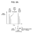
- FIGS. 8A and 8B depict laser emission as a function of time for a picosecond laser. Each emission is characterized by a pulse “burst” which may contain one or more sub-pulses. Times corresponding to pulse duration, separation between pulses, and separation between bursts are illustrated.
- FIG. 9 illustrates using defect lines which remain after the cut part is released to serve as sacrificial regions, arresting the propagation of cracks caused by impact to the edges of the part.
- FIG. 10A is an illustration of a cut part with internal defect lines being placed into ion-exchange, which adds enough stress to remove the perforated edges and form the desired edge chamfer.
- FIG. 10B an illustration of a cut part with internal defect lines being placed into ion-exchange (IOX) to release chamfered corners, similar to the illustration shown in FIG. 10A , but with only two defect line planes.
- IOX ion-exchange
- FIG. 10C is an illustration of a chamfer with many angles (more than 3 defect line planes.
- FIG. 11A provides a plot summarizing a INSTRON compression test results performed on the radial edge of one embodiment compliant edge finishing wheel (polishing wheel) using the edge probe;
- FIG. 11B provides a plot summarizing a INSTRON compression test results performed on the radial edge of a comparative stiff abradable finishing wheel using the same edge probe.
- FIG. 12A is a schematic diagram of the edge profile obtained when parts are laser cut with a 15° extended edge chamfer.
- FIG. 12B is a schematic diagram of the edge profile obtained when parts are laser cut with a 15° shortened edge chamfer.
- FIG. 12C is a schematic diagram of the edge profile obtained when parts are laser cut with a 45° edge chamfer.
- FIG. 12D displays a schematic diagram of the edge profile obtained when parts are laser cut with a 60° edge chamfer.
- FIG. 13A represents a composite fixed abrasive wheel, illustrating how wheel design utilizing different bonding materials, abrasives, and form factors may be used to concentrate finishing action to suit the incoming edge profile.
- FIG. 13B illustrates the concept of a compliant polishing wheel with provisions made for delivery of abrasive slurry through the spindle and wheel during operation.
- FIG. 14 illustrates schematically one embodiment of a constant force polishing Apparatus.
- FIG. 15A illustrates one embodiment of a compliant wheel 100 utilized for mechanically processing laser cut glass.
- FIGS. 15B-15E are microphotograps of the wheel of FIG. 15A .
- FIG. 16 illustrates nominal abrasive size estimation of the compliant polishing wheel of FIGS. 15A-15E .
- FIG. 17 illustrates exemplary edge strength (MPa) performance achieved with complient wheel polishing by the wheel 100 .
- FIGS. 18A and 18B are Apex Microscope Images, respectively, of laser cut substrate edges prior and post mechanical polishing by the wheel 100 of FIG. 15A .
- FIGS. 19A and 19B are Apex Microscope Images, respectively, of laser cut substrate edges prior and post mechanical polishing by the wheel according to one embodiment.
- FIGS. 20A and 20B are Apex Microscope Images, respectively, of laser cut substrate corners prior and post mechanical polishing by the wheel 100 , according to another embodiment.
- Embodiments described herein relate to processes of chamfering and/or beveling an edge of a glass substrate and other transparent materials of arbitrary shape using lasers.
- a first embodiment involves cutting the edge with the desired chamfer shape utilizing an ultra-short pulse laser that may be optionally followed by a other process steps for fully automated separation.
- the process fundamental step is to create fault lines on intersecting planes that delineate the desired edge shape and establish a path of least resistance for crack propagation and hence separation and detachment of the shape from its substrate matrix.
- This method essentially creates the shaped edge while cutting the part out of the main substrate.
- the laser separation method can be tuned and configured to enable manual separation, partial separation, or self-separation of the shaped edges out of the original substrate. The underlying principle to generate these fault lines is described in detail below and in U.S. Application No. 61/752,489 filed on Jan. 15, 2013.
- the object to be processed is irradiated with an ultra-short pulsed laser beam that is condensed into a high aspect ratio line focus that penetrates through the thickness of the substrate.
- the material is modified via nonlinear effects. It is important to note that without this high optical intensity, nonlinear absorption is not triggered. Below this intensity threshold, the material is transparent to the laser radiation and remains in its original state as shown in FIGS. 1A-1C .
- a narrow defect line is created (a few microns wide) and define the perimeter or shape to be separated in the next step.
- the particular laser method used has the advantage that in a single pass, it creates highly controlled full line perforation through the material, with extremely little ( ⁇ 75 ⁇ m, preferably ⁇ 60 ⁇ m, often ⁇ 50 ⁇ m, and in some embodiments ⁇ 40 ⁇ m) subsurface damage and debris generation. This is in contrast to the typical use of spot-focused laser to ablate material, where multiple passes are often necessary to completely perforate the glass thickness, large amounts of debris are formed from the ablation process, and more extensive sub-surface damage (>100 ⁇ m) and edge chipping occur.
- a method of laser drilling a material includes focusing a pulsed laser beam 2 into a laser beam focal line 2 b , viewed along the beam propagation direction.
- laser 3 (not shown) emits laser beam 2 , at the beam incidence side of the optical assembly 6 referred to as 2 a , which is incident onto the optical assembly 6 .
- the optical assembly 6 turns the incident laser beam into an extensive laser beam focal line 2 b on the output side over a defined expansion range along the beam direction (length l of the focal line).
- the planar substrate 1 to be processed is positioned in the beam path after the optical assembly overlapping at least partially the laser beam focal line 2 b of laser beam 2 .
- Reference 1 a designates the surface of the planar substrate facing the optical assembly 6 or the laser, respectively
- reference 1 b designates the reverse surface of substrate 1 usually spaced in parallel.
- the substrate thickness (measured perpendicularly to the planes 1 a and 1 b , i.e., to the substrate plane) is labeled with d.
- substrate 1 is aligned perpendicularly to the longitudinal beam axis and thus behind the same focal line 2 b produced by the optical assembly 6 (the substrate is perpendicular to the drawing plane) and viewed along the beam direction it is positioned relative to the focal line 2 b in such a way that the focal line 2 b viewed in beam direction starts before the surface 1 a of the substrate and stops before the surface 1 b of the substrate, i.e. still within the substrate.
- the focal line 2 b viewed in beam direction starts before the surface 1 a of the substrate and stops before the surface 1 b of the substrate, i.e. still within the substrate.
- the extensive laser beam focal line 2 b thus generates (in case of a suitable laser intensity along the laser beam focal line 2 b which is ensured due to the focusing of laser beam 2 on a section of length l, i.e. a line focus of length l) an extensive section 2 c viewed along the longitudinal beam direction, along which an induced absorption is generated in the substrate material which induces a defect line or crack formation in the substrate material along section 2 c .
- the defect line formation is not only local, but over the entire length of the extensive section 2 c of the induced absorption.
- the length of section 2 c (i.e., after all, the length of the overlapping of laser beam focal line 2 b with substrate 1 ) is labeled with reference L.
- the average diameter or the average extension of the section of the induced absorption (or the sections in the material of substrate 1 undergoing the defect line formation) is labeled with reference D.
- This average extension D basically corresponds to the average diameter ⁇ of the laser beam focal line 2 b , that is, an average spot diameter in a range of between about 0.1 ⁇ m and about 5 ⁇ m.
- FIG. 2A shows, substrate material transparent for the wavelength ⁇ of laser beam 2 is heated due to the induced absorption along the focal line 2 b .
- FIG. 2B outlines that the warming material will eventually expand so that a correspondingly induced tension leads to micro-crack formation, with the tension being the highest at surface 1 a.
- the individual focal lines to be positioned on the substrate surface along parting line 5 should be preferably generated using the optical assembly described below (hereinafter, the optical assembly is alternatively also referred to as laser optics).
- the roughness results particularly from the spot size or the spot diameter of the focal line.
- certain requirements are usually imposed on the numerical aperture of laser optics 6 . These requirements are met by laser optics 6 described below.
- the laser beam should preferably illuminate the optics up to the required aperture, which is typically achieved by means of beam widening using widening telescopes between laser and focusing optics.
- the spot size should not vary too strongly for the purpose of a uniform interaction along the focal line. This can, for example, be ensured (see the embodiment below) by illuminating the focusing optics only in a small, circular area so that the beam opening and thus the percentage of the numerical aperture only vary slightly.
- FIG. 3A section perpendicular to the substrate plane at the level of the central beam in the laser beam bundle of laser radiation 2 ; here, too, laser beam 2 is incident perpendicularly to the substrate plane, i.e. angle ⁇ is 0° so that the focal line 2 b or the extensive section of the induced absorption 2 c is parallel to the substrate normal
- the laser radiation 2 a emitted by laser 3 is first directed onto a circular aperture 8 which is completely opaque for the laser radiation used.
- Aperture 8 is oriented perpendicular to the longitudinal beam axis and is centered on the central beam of the depicted beam bundle 2 a .
- the diameter of aperture 8 is selected in such a way that the beam bundles near the center of beam bundle 2 a or the central beam (here labeled with 2 a Z) hit the aperture and are completely absorbed by it. Only the beams in the outer perimeter range of beam bundle 2 a (marginal rays, here labeled with 2 a R) are not absorbed due to the reduced aperture size compared to the beam diameter, but pass aperture 8 laterally and hit the marginal areas of the focusing optic elements of the optical assembly 6 , which is designed as a spherically cut, bi-convex lens 7 here.
- Lens 7 centered on the central beam is deliberately designed as a non-corrected, bi-convex focusing lens in the form of a common, spherically cut lens. Put another way, the spherical aberration of such a lens is deliberately used.
- aspheres or multi-lens systems deviating from ideally corrected systems, which do not form an ideal focal point but a distinct, elongated focal line of a defined length can also be used (i.e., lenses or systems which do not have a single focal point). The zones of the lens thus focus along a focal line 2 b , subject to the distance from the lens center.
- the diameter of aperture 8 across the beam direction is approximately 90% of the diameter of the beam bundle (beam bundle diameter defined by the extension to the decrease to 1/e) and approximately 75% of the diameter of the lens of the optical assembly 6 .
- the focal line 2 b of a not aberration-corrected spherical lens 7 generated by blocking out the beam bundles in the center is thus used.
- FIG. 3A shows the section in one plane through the central beam, the complete three-dimensional bundle can be seen when the depicted beams are rotated around the focal line 2 b.
- This focal line is that the conditions (spot size, laser intensity) along the focal line, and thus along the desired depth in the material, vary and that therefore the desired type of interaction (no melting, induced absorption, thermal-plastic deformation up to crack formation) may possibly only be selected in a part of the focal line. This means in turn that possibly only a part of the incident laser light is absorbed in the desired way. In this way, the efficiency of the process (required average laser power for the desired separation speed) is impaired on the one hand, and on the other hand the laser light might be transmitted into undesired deeper places (parts or layers adherent to the substrate or the substrate holding fixture) and interact there in an undesirable way (heating, diffusion, absorption, unwanted modification).
- FIG. 3B-1-4 show (not only for the optical assembly in FIG. 3A , but basically also for any other applicable optical assembly 6 ) that the laser beam focal line 2 b can be positioned differently by suitably positioning and/or aligning the optical assembly 6 relative to substrate 1 as well as by suitably selecting the parameters of the optical assembly 6 :
- the length l of the focal line 2 b can be adjusted in such a way that it exceeds the substrate thickness d (here by factor 2 ). If substrate 1 is placed (viewed in longitudinal beam direction) centrally to focal line 2 b , an extensive section of induced absorption 2 c is generated over the entire substrate thickness.
- a focal line 2 b of length l is generated which corresponds more or less to the substrate extension d.
- the length L of the extensive section of induced absorption 2 c (which extends here from the substrate surface to a defined substrate depth, but not to the reverse surface 1 b ) is smaller than the length l of focal line 2 b .
- the focal line thus starts within the substrate and extends over the reverse surface 1 b to beyond the substrate.
- FIG. 4 depicts another applicable optical assembly 6 .
- the basic construction follows the one described in FIG. 3A so that only the differences are described below.
- the depicted optical assembly is based on the use of optics with a non-spherical free surface in order to generate the focal line 2 b , which is shaped in such a way that a focal line of defined length l is formed.
- aspheres can be used as optic elements of the optical assembly 6 .
- a so-called conical prism also often referred to as axicon
- An axicon is a special, conically cut lens which forms a spot source on a line along the optical axis (or transforms a laser beam into a ring).
- the layout of such an axicon is principally known to one skilled in the art; the cone angle in the example is 10°.
- the apex of the axicon labeled here with reference 9 is directed towards the incidence direction and centered on the beam center.
- substrate 1 (here aligned perpendicularly to the main beam axis) can be positioned in the beam path directly behind axicon 9 .
- FIG. 4 shows, it is also possible to shift substrate 1 along the beam direction due to the optical characteristics of the axicon without leaving the range of focal line 2 b .
- the extensive section of the induced absorption 2 c in the material of substrate 1 therefore extends over the entire substrate depth d.
- the depicted layout is subject to the following restrictions: As the focal line of axicon 9 already starts within the lens, a significant part of the laser energy is not focused into part 2 c of focal line 2 b , which is located within the material, in case of a finite distance between lens and material. Furthermore, length l of focal line 2 b is related to the beam diameter for the available refraction indices and cone angles of axicon 9 , which is why, in case of relatively thin materials (several millimeters), the total focal line may be too long, having the effect that the laser energy is again not specifically (or not totally) focused into the material.
- FIG. 5A depicts such an optical assembly 6 in which a first optical element (viewed along the beam direction) with a non-spherical free surface designed to form an extensive laser beam focal line 2 b is positioned in the beam path of laser 3 .
- this first optical element is an axicon 10 with a cone angle of 5°, which is positioned perpendicularly to the beam direction and centered on laser beam 3 .
- the apex of the axicon is oriented towards the beam direction.
- a second, focusing optical element here the plano-convex lens 11 (the curvature of which is oriented towards the axicon), is positioned in beam direction at a distance z 1 from the axicon 10 .
- the distance z 1 in this case approximately 300 mm, is selected in such a way that the laser radiation formed by axicon 10 circularly incides on the marginal area of lens 11 .
- Lens 11 focuses the circular radiation on the output side at a distance z 2 , in this case approximately 20 mm from lens 11 , on a focal line 2 b of a defined length, in this case 1.5 mm.
- the effective focal length of lens 11 is 25 mm here.
- the circular transformation of the laser beam by axicon 10 is labeled with the reference SR.
- FIG. 5B depicts the formation of the focal line 2 b or the induced absorption 2 c in the material of substrate 1 according to FIG. 5A in detail.
- the optical characteristics of both elements 10 , 11 as well as the positioning of them is selected in such a way that the extension 1 of the focal line 2 b in beam direction is exactly identical with the thickness d of substrate 1 . Consequently, an exact positioning of substrate 1 along the beam direction is required in order to position the focal line 2 b exactly between the two surfaces 1 a and 1 b of substrate 1 , as shown in FIG. 5B .
- the focal line is formed at a certain distance from the laser optics, and if the greater part of the laser radiation is focused up to a desired end of the focal line.
- this can be achieved by illuminating a primarily focusing element 11 (lens) only circularly on a required zone, which, on the one hand, serves to realize the required numerical aperture and thus the required spot size, on the other hand, however, the circle of diffusion diminishes in intensity after the required focal line 2 b over a very short distance in the center of the spot, as a basically circular spot is formed. In this way, the defect line formation is stopped within a short distance in the required substrate depth.
- a combination of axicon 10 and focusing lens 11 meets this requirement.
- the axicon acts in two different ways: due to the axicon 10 , a usually round laser spot is sent to the focusing lens 11 in the form of a ring, and the asphericity of axicon 10 has the effect that a focal line is formed beyond the focal plane of the lens instead of a focal point in the focal plane.
- the length l of focal line 2 b can be adjusted via the beam diameter on the axicon.
- the numerical aperture along the focal line on the other hand, can be adjusted via the distance z 1 axicon-lens and via the cone angle of the axicon. In this way, the entire laser energy can be concentrated in the focal line.
- the circular illumination still has the advantage that, on the one hand, the laser power is used in the best possible way as a large part of the laser light remains concentrated in the required length of the focal line, on the other hand, it is possible to achieve a uniform spot size along the focal line—and thus a uniform separation process along the focal line—due to the circularly illuminated zone in conjunction with the desired aberration set by means of the other optical functions.
- a collimating lens 12 serves to adjust the circular illumination of focusing lens 11 very tightly.
- the focal length f′ of collimating lens 12 is selected in such a way that the desired circle diameter dr results from distance z 1 a from the axicon to the collimating lens 12 , which is equal to f′.
- the desired width br of the ring can be adjusted via the distance z 1 b (collimating lens 12 to focusing lens 11 ).
- the small width of the circular illumination leads to a short focal line. A minimum can be achieved at distance f′.
- the optical assembly 6 depicted in FIG. 6 is thus based on the one depicted in FIG. 5A so that only the differences are described below.
- the collimating lens 12 here also designed as a plano-convex lens (with its curvature towards the beam direction) is additionally placed centrally in the beam path between axicon 10 (with its apex towards the beam direction), on the one side, and the plano-convex lens 11 , on the other side.
- the distance of collimating lens 12 from axicon 10 is referred to as z 1 a
- the distance of focusing lens 11 from collimating lens 12 as z 1 b
- the distance of the generated focal line 2 b from the focusing lens 11 as z 2 (always viewed in beam direction).
- the circular radiation SR formed by axicon 10 which incides divergently and under the circle diameter dr on the collimating lens 12 , is adjusted to the required circle width br along the distance z 1 b for an at least approximately constant circle diameter dr at the focusing lens 11 .
- a very short focal line 2 b is supposed to be generated so that the circle width br of approximately 4 mm at lens 12 is reduced to approximately 0.5 mm at lens 11 due to the focusing properties of lens 12 (circle diameter dr is 22 mm in the example).
- separation can occur via: manual or mechanical stress applied on or around the fault line; the stress or pressure should create tension that pulls both sides of the fault line apart and break the areas that are still bonded together. Separation depends on several of the process parameters, such as laser scan speed, laser power, parameters of lenses, pulse width, repetition rate, etc.
- FIG. 7A gives an overview of the processes described in the present application.
- the developed process relies on the material transparency to the laser wavelength in linear regime, or low laser intensity, which allows maintenance of a clean and high (or pristine) surface quality and on the reduced subsurface damage created by the area of high intensity around the laser focus.
- One of the important parameters of this process is the high aspect ratio of the defect created by the ultra-short pulsed laser. It allows creation of a long and deep fault or defect line that can extend from the top to the bottom surfaces of the material to be cut and chamfered. In principle, each defect can be created by a single pulse and if necessary, additional pulses can be used to increase the extension of the affected area (depth and width).
- the optical method of forming the line focus can take multiple forms, using donut shaped laser beams and spherical lenses, axicon lenses, diffractive elements, or other methods to form the linear region of high intensity.
- the type of laser (picosecond, femtosecond, etc.) and wavelength (IR, green, UV, etc.) can also be varied, as long as sufficient optical intensities are reached to create breakdown of the substrate material.
- an ultra-short pulsed laser is used to create this high aspect ratio vertical defect line in a consistent, controllable and repeatable manner.
- This embodiment utilizes an axicon lens element in an optical lens assembly to create a region of high aspect ratio taper-free microchannel using ultra-short (picoseconds or femtosecond duration) Bessel beams.
- the axicon condenses the laser beam into a region of cylindrical shape and high aspect ratio (long length and small diameter). Due to the high intensity created with the condensed laser beam, nonlinear interaction of the laser electromagnetic field and the material occurs and the laser energy is transferred to the substrate.
- the method to cut and separate the glass substrate is essentially based on creating a fault line on the material to be processed with an ultra-short pulsed laser.
- the specific chosen process parameters will depend on the material properties (absorption, CTE, stress, composition, etc.) and laser parameters chosen for processing.
- the created fault line is not enough to separate it automatically and a secondary step may be necessary. If so desired, in the case of non-chemically strengthened glass, separation can be achieved, after the creation of a defect line, by application of mechanical force.
- the process to produce chamfered edges can be modified as illustrated in FIG. 7A .
- To separate the glass and to form a good quality chamfered edge for example, in one embodiment we create three separate planes of defect lines that intersect and define the boundaries of the shape. A different shape can be created by using, for example, just two intersecting defect line planes as illustrated in FIG.
- the flat part of the edge has to be broken/separated without any defect lines. It should be possible to separate the corner at the defect line plane with the proper combination of defect line characteristics and treatment with IOX bath.
- the defect lines may be formed at an ⁇ i , with respect to the normal to the flat surface of the glass substrate, In some embodiments angle 0° ⁇ i ⁇ 90°.
- a chamfered edge on the bottom of FIG. 7B was produced by 3 intersecting planes, each containing a plurality of defect lines.
- a process for the purpose of cutting glass or other transparent brittle materials, a process was developed that uses a (for example, 1064 nm, or 532 nm, 266 nm, or 261 nm) picosecond laser in combination with line-focus beam forming optics to create lines of damage (i.e., defect lines) in the substrates.
- a sample Corning® Gorilla® Glass code 2320 substrate with 0.7 mm thickness is positioned so that it is within the line-focus.
- the optical intensities in the line region can easily be high enough to create non-linear absorption in the material.
- a region of damaged, ablated, vaporized, or otherwise modified material is created that approximately follows the linear region of high intensity.
- each “burst” may contain multiple pulses (also termed sub-pulses herein) of very short duration (for example, ⁇ 10 psec).
- Each sub-pulse or individual pulse within a burst is separated in time by, for example by approximately 20 nsec (50 MHz), with the time often governed by the laser cavity design.
- the time between each “burst” will be much longer, often ⁇ 5 ⁇ sec, for a laser repetition rate of ⁇ 200 kHz.
- the exact timings, pulse durations, and repetition rates can vary depending on the laser design. But short pulses ( ⁇ 15 psec) of high intensity have been shown to work well with this technique.
- each burst of pulses may contain two pulses (also referred to as sub-pulses herein) or more (such as 3 pulses, 4 pulses, 5 pulses, 10 pulses, 15 pulses, 20 pulses, 22 pulses, 25 pulses, or more pulses within a burst) separated from each other by a duration in a range of between about 1 nsec and about 50 nsec, for example, 10 nsec to 50 nsec (e.g., about 20 nsec, or 30 nsec), and the burst repetition frequency (i.e., separation between the first pulses in two subsequent bursts) can be in a range of between about 1 kHz and about 200 kHz.
- the pulsed laser beam can have a wavelength selected such that the material is substantially transparent at this wavelength.
- a material is substantially transparent to the laser wavelength when the absorption is less than about 50% (e.g. ⁇ 40%), more preferably less than 10%, and even more preferably less than about 1% per mm of material depth at this wavelength.
- This wavelength may be, for example, 1064 nm, 532 nm, 355 nm, or 266 nanometers.
- the average laser power measured at the material can be greater than 40 microJoules per mm thickness of material, for example between 40 microJoules/mm and 1000 microJoules, for example 100-900 ⁇ J/mm, or between 100 and 650 microJoules/mm, with 200-400 ⁇ J/mm being preferable.
- the picosecond laser creates a “burst” 500 of pulses 500 A, sometimes also called a “burst pulse”.
- Each “burst” 500 may contain multiple pulses 500 A of very short duration T d up to 100 psec (for example, 0.1 psec, 5 psec, 10 psec, 15 psec, 18 ps, 20 ps, 22 ps, 25 ps, 30 ps, 50 ps, 75 ps, or therebetween).
- each pulse 500 A within a single burst 500 can also be termed “sub-pulses,” which simply denotes the fact that they occur within a single burst of pulses.
- the energy or intensity of each laser pulse 500 A within the burst may not be equal to that of other pulses within the bust, and the intensity distribution of the multiple pulses within a burst 500 often follows an exponential decay in time governed by the laser design.
- each pulse 500 A within the burst 500 of the exemplary embodiments described herein are separated in time from the subsequent pulse in the burst by a duration T p from 1 nsec to 50 nsec (e.g. 10-50 ns, or 10-30 nsec, with the time often governed by the laser cavity design.
- the time separation T p between each pulses (pulse-to-pulse separation) within a burst 500 is relatively uniform ( ⁇ 10%).
- each pulse is separated in time from the subsequent pulse by approximately 20 nsec (50 MHz).
- the pulse to pulse separation T p within a burst is maintained within about ⁇ 10%, or is about ⁇ 2 nsec.
- the time between each “burst” i.e., time separation T b between bursts
- will be much longer e.g., 0.25 ⁇ T b ⁇ 1000 microseconds, for example 1-10 microseconds, or 3-8 microseconds,).
- the laser repetition rate is also referred to as burst repetition frequency herein, and is defined as the time between the first pulse in a burst to the first pulse in the subsequent burst.
- the burst repetition frequency is in a range of between about 1 kHz and about 4 MHz. More preferably, the laser repetition rates can be, for example, in a range of between about 10 kHz and 650 kHz.
- the time T b between the first pulse in each burst to the first pulse in the subsequent burst may be 0.25 microsecond (4 MHz repetition rate) to 1000 microseconds (1 kHz repetition rate), for example 0.5 microseconds (2 MHz repetition rate) to 40 microseconds (25 kHz repetition rate), or 2 microseconds (500 kHz repetition rate) to 20 microseconds (50 kHz repetition rate).
- the exact timings, pulse durations, and repetition rates can vary depending on the laser design, but short pulses (T d ⁇ 20 psec and preferably T d ⁇ 15 psec) of high intensity have been shown to work particularly well.
- the required energy to modify the material can be described in terms of the burst energy—the energy contained within a burst (each burst 500 contains a series of pulses 500 A), or in terms of the energy contained within a single laser pulse (many of which may comprise a burst).
- the energy per burst can be from 25-750 ⁇ J, more preferably 50-500 ⁇ J, 50-250 ⁇ u. In some embodiments the energy per burst is 100-250 ⁇ J.
- the energy of an individual pulse within the burst will be less, and the exact individual laser pulse energy will depend on the number of pulses 500 A within the burst 500 and the rate of decay (e.g., exponential decay rate) of the laser pulses with time as shown in FIGS.
- each individual laser pulse 500 A will contain less energy than if the same burst pulse 500 had only 2 individual laser pulses.
- a laser capable of generating such burst pulses is advantageous for cutting or modifying transparent materials, for example glass.
- the use of a burst pulse sequence that spreads the laser energy over a rapid sequence of sub-pulses allows access to larger timescales of high intensity interaction with the material than is possible with single-pulse lasers.
- a single-pulse can be expanded in time, as this is done the intensity within the pulse must drop as roughly one over the pulse width. Hence if a 10 psec single pulse is expanded to a 10 nsec pulse, the intensity drops by roughly three orders of magnitude.
- the intensity during each sub-pulse 500 A can remain very high—for example three 10 psec pulses 500 A spaced apart in time by approximately 10 nsec still allows the intensity within each pulse to be approximately three times higher than that of a single 10 psec pulse, while the laser is allowed to interact with the material over a timescale that is now three orders of magnitude larger.
- This adjustment of multiple pulses 500 A within a burst thus allows manipulation of time-scale of the laser-material interaction in ways that can facilitate greater or lesser light interaction with a pre-existing plasma plume, greater or lesser light-material interaction with atoms and molecules that have been pre-excited by an initial or previous laser pulse, and greater or lesser heating effects within the material that can promote the controlled growth of microcracks.
- the required amount of burst energy to modify the material will depend on the substrate material composition and the length of the line focus used to interact with the substrate. The longer the interaction region, the more the energy is spread out, and the higher the burst energy that will be required.
- the substrate or transparent material has sufficient stress (e.g. with post-ion exchanged glass), then the part will spontaneously crack and separate along the path of perforated damage traced out by the laser process.
- the picosecond laser will simply form damage tracks (i.e., defect lines or perforations) in the piece.
- the defect lines or damage tracks usually have an interior diameter of not greater than 5 ⁇ m.
- the defect lines generally take the form of holes with interior dimensions of not greater than 5 microns, for example 0.5-1.5 microns, or 0.2 microns to 2 microns (for example, in some embodiments, 0.2 to 0.7 microns, or 0.3 to 0.6 microns).
- the holes are very small (single microns or less) in dimension.
- the holes or defect lines can perforate the entire thickness of the material, and may or may not be a continuous opening throughout the depth of the material.
- FIG. 1C shows an example of such tracks perforating the entire thickness of a piece of 700 ⁇ m thick unstrengthened Gorilla® Glass substrate.
- the perforations or damage tracks are observed through the side of a cleaved edge.
- the tracks through the material are not necessarily through holes—there are often regions of glass that plug the holes, but they are generally small in size.
- the lateral spacing (pitch) between these holes is determined by the pulse rate of the laser as the substrate is translated underneath the focused laser beam. Only a single picosecond laser pulse burst is necessary to form an entire hole, although multiple pulses may be used if desired.
- the laser can be triggered to fire at longer or shorter intervals.
- the laser triggering generally is synchronized with the stage driven motion of the part beneath the beam, so laser pulses are triggered at a fixed interval, such as every 1 ⁇ m, or every 5 ⁇ m.
- the exact spacing is determined by the material properties that facilitate crack propagation from perforated hole to perforated hole, given the stress level in the substrate.
- the laser power and lens focal length (which determines the filament length and hence power density) are particularly critical parameters to ensure full penetration of the glass and low micro-cracking.
- Processes disclosed herein can cut glass at a cutting speed of 0.25 m/sec, or faster.
- a cut speed is the rate the laser beam moves relative to the surface of the transparent material (e.g., glass) while creating multiple holes or modified regions.)
- High cut speeds such as, for example 250 mm/sec 400 mm/sec, 500 mm/sec, 750 mm/sec, 1 m/sec, 1.2 m/sec, 1.5 m/sec, or 2 m/sec, or even 3.4 m/sec to 4 m/sec are often desired in order to minimize capital investment for manufacturing, and to optimize equipment utilization rate.
- the laser power is equal to the burst energy multiplied by the burst repetition frequency (rate) of the laser.
- the damage tracks are typically spaced apart by 1-25 microns, in some embodiments the spacing is preferably 3 microns or larger—for example 3-12 microns, or for example 5-10 microns.
- 3 micron hole pitch corresponds to a pulse burst laser with at least 100 kHz burst repetition rate.
- a 3 micron pitch corresponds to a burst-pulsed laser with at least 200 kHz burst repetition rate.
- a pulse burst laser that produces at least 40 ⁇ J/burst at 200 kHz, and cuts at a 600 mm/s cutting speed needs to have laser power of at least 8 Watts. Higher cut speeds therefore require even higher laser powers.
- a 0.4 m/sec cut speed at 3 ⁇ m pitch and 40 ⁇ J/burst would require at least a 5 Watt laser
- a 0.5 m/sec cut speed at 3 ⁇ m pitch and 40 ⁇ J/burst would require at least a 6 Watt laser.
- the laser power of the pulse burst is 6 watts or higher, more preferably at least 8 Watts or higher, and even more preferably at least 10 W or higher.
- the optimal pitch between damage tracks and the exact burst energy is material dependent, and can be determined empirically. However, it should be noted that raising the laser pulse energy or making the damage tracks at a closer pitch are not conditions that always make the substrate material separate better or with improved edge quality. Too dense a pitch (for example ⁇ 0.1 micron, in some exemplary embodiments ⁇ 1 ⁇ m, or in some embodiments ⁇ 2 ⁇ m) between damage tracks can sometimes inhibit the formation of nearby subsequent damage tracks, and often can inhibit the separation of the material around the perforated contour, and may also result in increased unwanted micro cracking within the glass.
- Too dense a pitch for example ⁇ 0.1 micron, in some exemplary embodiments ⁇ 1 ⁇ m, or in some embodiments ⁇ 2 ⁇ m
- Too long a pitch may result in “uncontrolled microcracking”—i.e., where instead of propagating from hole to hole the microcracks propagate along a different path, and cause the glass to crack in a different (undesirable) direction. This may ultimately lower the strength of the separated glass part, since the residual microcracks will acts as flaws which weaken the glass.
- Too high a burst energy (e.g., >2500 ⁇ J/burst, and in some embodiments >500 ⁇ J/burst) used to form each damage track can cause “healing” or re-melting of already formed microcracks of adjacent damage tracks, which will inhibit separation of the glass. Accordingly, it is preferred that burst energy be ⁇ 2500 ⁇ J/burst, for example, ⁇ 500 ⁇ J/burst. Also, using a burst energy that is too high can cause formation of microcracks that are extremely large and create flaws which reduce the edge strength of the parts after separation. Too low a burst energy ( ⁇ 40 ⁇ J/burst) may result in no appreciable damage track formed within the glass, and hence very high separation strength or complete inability to separate along the perforated contour.
- a burst energy e.g., >2500 ⁇ J/burst, and in some embodiments >500 ⁇ J/burst
- Typical exemplary cutting rates (speeds) enabled by this process are, for example, 0.25 msec and higher.
- the cutting rates are at least 300 mm/sec.
- the cutting rates are at least 400 mm/sec, for example 500 mm/sec to 2000 mm/sec, or higher.
- the picosecond (ps) laser utilizes pulse bursts to produce defect lines with periodicity between 0.5 microns and 13 microns, e.g. 0.5 and 3 microns.
- the pulsed laser has laser power of 10 W-100 W and the material and/or the laser beam are translated relative to one another at a rate of at least 0.25 msec, for example at the rate of 0.25 to 0.35 msec, or 0.4 msec to 5 msec.
- each pulse burst of the pulsed laser beam has an average laser energy measured at the workpiece greater than 40 microJoules per burst mm thickness of workpiece.
- each pulse burst of the pulsed laser beam has an average laser energy measured at the workpiece greater of less than 2500 microJoules per burst per mm thickness of workpiece, and preferably lass than about 2000 microJoules per burst per mm, and in some embodiments less than 1500 microJoules per burst per mm thickness of workpiece, for example not more than 500 microJoules per burst per mm thickness of workpiece.
- volumetric pulse energy density ( ⁇ j/ ⁇ m 3 ) is required for perforating alkaline earth boro-aluminosilicate glasses with low or no alkali containing glasses as compared to that for glasses such as Corning Gorilla®.
- This can be achieved, for example, by utilizing pulse burst lasers, preferably with at least 2 pulses per burst and providing volumetric energy densities within the alkaline earth boro-aluminosilicate glasses (with low or no alkali) of about 0.05 ⁇ J/ ⁇ m 3 or higher, e.g., at least 0.1 ⁇ J/ ⁇ m 3 , for example 0.1-0.5 ⁇ J/ ⁇ m 3 .
- the laser produces pulse bursts with at least 2 pulses per burst.
- the pulsed laser has laser power of 10 W-150 W (e.g., 10-100 W) and produces pulse bursts with at least 2 pulses per burst (e.g., 2-25 pulses per burst).
- the pulsed laser has the power of 25 W-60 W, and produces pulse bursts with at least 2-25 pulses per burst, and periodicity or distance between the adjacent defect lines produced by the laser bursts is 2-10 microns.
- the pulsed laser has laser power of 10 W-100 W, produces pulse bursts with at least 2 pulses per burst, and the workpiece and the laser beam are translated relative to one another at a rate of at least 0.25 m/sec. In some embodiments the workpiece and/or the laser beam are translated relative to one another at a rate of at least 0.4 m/sec.
- pitches of 3-7 microns can work well, with pulse burst energies of about 150-250 ⁇ J/burst, and burst pulse numbers that range from 2-15, and preferably with pitches of 3-5 microns and burst pulse numbers (number of pulses per burst) of 2-5.
- laser powers 15-84 Watts, with 30-45 Watts often being sufficient.
- laser powers between 10 and 100 W are preferred to achieve cutting speeds from 0.2-1 m/sec, with laser powers of 25-60 Watts being sufficient (and optimum) for many glasses.
- laser powers should preferably be 10 W-150 W, with burst energy of 40-750 ⁇ J/burst, 2-25 bursts per pulse (depending on the material that is cut), and hole separation (or pitch) of 3 to 15 ⁇ m, or 3-10 ⁇ m.
- the pulsed laser produces 10-100 W of power, for example 25 W to 60 Watts, and produces pulse bursts at least 2-25 pulses per burst and the distance between the defect lines is 2-15 microns; and the laser beam and/or workpiece are translated relative to one another at a rate of at least 0.25 m/sec, in some embodiments at least 0.4 m/sec, for example 0.5 m/sec to 5 m/sec, or faster.
- the first method is to use the picosecond laser only to create defect lines and forming a fault line following the desired shape (in this case a chamfered edge).
- mechanical separation can be accomplished by using a breaking plier, manually bending the part, or any method that creates tension that initiates and propagates the separation along the fault line.
- Pulse repetition rate of the laser 200 kHz.
- the presence of the remaining defect line inside the glass can be beneficial to arrest the propagation of cracks when the edge is impacted.
- the defect line planes can be used to serve as damage arrest locations, in effect creating a “sacrificial” edge part of the region of glass that is on the outside relative to the defect lines.
- creation of sacrificial edges that simply have an extra defect line to the interior of the separated edge, or a set of defect lines that intersect to form a more complex interior bevel inside of the true edge may be a method of creating increased part reliability without the need for any physical chamfer feature on the outside edge of the part, nor any mechanical grinding and polishing to create that feature.
- Some options for this type of sacrificial edge are shown in FIG. 9 . Since the picosecond laser process described above creates each defect line in a single pass and at speeds of up to 1 m/s, it is very easy and cost-effective to create these extra “damage stop” lines.
- Pulse repetition rate of the laser 200 k Hz.
- the laser for example the picosecond laser described above creates the fault line and cuts the glass.
- the separation of the outside glass edge pieces formed by the defect lines need not be done by a mechanical force.
- Laser processing itself can create enough stress to pop the small chamfer regions or corner pieces off of the part.
- This laser cutting process utilizes a line focus and can cut glass or other transparent materials at speeds of 200-1000 mm/sec, either normal or at an angle to create a chamfer shaped edge.
- the intense laser beam(s) cuts and separates the thin glass, causing less than 60 ⁇ m of subsurface damage with a less than 400 nm Ra surface roughness.
- sub-surface damage is less than 30 ⁇ m with less than 200 nm Ra surface roughness.
- the laser glass cutting is accomplished to within microns of the final product shape, now allowing the final finishing process to remove only minimal glass stock material to meet customer edge finish, strength and edge impact requirements. This process can cut stacks of glass normal to the glass surface allowing stack finishing to occur.
- the glass part separated from a glass substrate is sent for chemical strengthening in an ion exchange process.
- Ion exchange itself can create enough stress to prompt peeling or separation at the chamfer regions or corners of the part.
- the introduction of new ions into the glass surface can create enough stress to cause the outside corner pieces to peel or separate.
- the high temperature salt bath used in the ion exchange process can provide thermal stress sufficient to induce peeling or separation along the fault line to provide a chamfered or otherwise shaped edge. In either case, the ultimate result is an edge that more closely follows the interior defect lines to form the desired chamfer shape see FIG. 10A-10C ).
- FIG. 10A is an illustration of a cut part with internal defect lines being placed into ion-exchange, which adds enough stress to remove the perforated edges and form the desired edge chamfer.
- FIG. 10B an illustration of a cut part with internal defect lines being placed into ion-exchange (IOX) to release chamfered corners, similar to the illustration shown in FIG. 10A , but with only two defect line planes.
- FIG. 10C is an illustration of a chamfer with many angles (more than 3 defect line planes).
- the laser cut edge may be edge finished to remove damage remaining on the edges in the areas exposed to laser cutting and separation.
- the edge strength of substrates prepared by laser cutting may be increased considerably through the use of a significantly compliant abrasive edge finishing wheel (also referred herein as a polishing wheel) during edge finishing.
- a significantly compliant abrasive edge finishing wheel also referred herein as a polishing wheel
- the use of the compliant (bulk modulus of elasticity of 0.1 GPa to 5 GPa) abrasive polishing wheel effects material removal in the partial ductile regime (concentrating, for example, such removal on the corners formed by the parallel substrate surfaces and the substrate edge of the workpiece).
- the polishing wheel is a compliant fixed abrasive edge finishing wheel (the abrasive is potted in, and does not move). In some embodiments the polishing wheel is a compliant abrasive edge finishing wheel where the abrasive is externally delivered and is not fixed, but the polishing wheel provides abrasive edge finishing by carrying the abrasive.
- the polishing wheel body is still compliant with the bulk modulus of elasticity of 0.1 GPa to 5 GPa.
- the polishing wheel is a compliant fixed abrasive edge finishing wheel and the additional abrasive is externally delivered, providing abrasive edge finishing by carrying the abrasive.
- the polishing wheel body in such embodiments is still compliant with the bulk modulus of elasticity of 0.1 GPa to 5 GPa.
- the method utilizes a constant force edge finishing process employing a compliant fixed abrasive wheel 100 (also referred to as a polishing wheel, or finishing wheel 100 herein) made compliant by virtue of a construction featuring a soft (not metal or ceramic) abradable bonding material bearing a quantity of abrasive of a particular type, size, concentration, and friability to provide the desired edge finishing.
- the bonding material may be, for example, a polymeric material.
- the compliant, fixed abrasive wheel(s) 100 is(are) affixed to an apparatus capable of rotating the wheel(s) at high speeds and simultaneously bringing it(them) into contact with the substrate edge(s) intended for finishing.
- compliance refers to the relative mechanical resistance of the fixed finishing wheel to lateral force such as that delivered by an external source such as an air cylinder, simple spring, or other such device and transmitted through a defined contact area such as a representative substrate edge as occurs in the course of edge finishing.
- compliance was quantified employing a commercially available Instron (model number 5500R) testing system set up to deliver compressive force to the fixed finishing wheel structure through a test probe designed to replicate a typical rectangular substrate edge. The wheel is mounted vertically and the probe brought to its surface at its outside diameter thereby enabling compressive force to be applied to the wheel radially.
- a compliant abrasive wheel 100 offers relatively low initial resistance to the compressive force transmitted radially through the edge probe in such testing thereby enabling considerable penetration of the substrate edge into the fixed wheel material.
- the polishing wheel is compliant—i.e., it has a bulk modulus of elasticity of 0.1 GPa to 5 GPa (e.g., 1 to 4 GPa, or 2 to 4 GPa).
- the polishing wheel is compliant, such that at a probe extension (effectively equivalent to the penetration into the wheel) of 1 millimeter the resistance offered by the compliant wheel is not greater than 10 kg f , e.g., 0.1 kg f to 6 kg f (dry, without application of lubricant).
- the resistance offered by the compliant wheel is 3.73 kg f . From FIG. 11A it can be seen that at a probe extension (effectively equivalent to the penetration into the wheel) of 1 millimeter the resistance offered by the compliant wheel is 3.73 kg f . From FIG.
- Abrasive particle size in the fixed abrasive wheel 100 used in this embodiment was determined by optical microscopy to be 5-10 ⁇ m and was present in a 2.5-5% concentration by volume. Edge finishing using this methodology was not limited, however, to these abrasive sizes and concentration ranges. Abrasive particle size ranging from 0.1 to 100 ⁇ m in concentrations ranging from 2.5 to 50% volume concentration in a wide range of abrasive friability (relative toughness) can also be employed. Furthermore, in this exemplary embodiment abrasive toughness of the abrasives is considered to be in the upper range of toughness (less friable); it would be considered in the MBG 620-MBG 660 range on the ranking scale.
- compliant abrasive wheel 100 may utilize (or be made of) a large range of abrasive materials (i.e., natural diamond, synthetic diamond, zirconium, cerium oxide, silicon carbide, and many others).
- abrasive materials i.e., natural diamond, synthetic diamond, zirconium, cerium oxide, silicon carbide, and many others.
- the compliant, fixed abrasive wheel(s) 100 is(are) affixed to an apparatus capable of rotating the wheel(s) at high speeds and simultaneously bringing it(them) into contact with the substrate edge(s) intended for finishing.
- Wheel rotation speed is used to impart (as well as gauge) the rate of contact of abrasive wheel to substrate (or work piece) edge during edge finishing. While wheel speed is typically measured in revolutions per minute, the interaction of abrasive with substrate edge as expressed by the number of contacts that individual abrasive particles make with the substrates being finished is also important. This rate of contact is expressed as a linear rate such as surface feet (or meters) per minute. In this exemplary embodiment edge polishing of the workpiece was accomplished using 101.6 mm diameter compliant finishing wheels 100 rotated at wheel speeds ranging from 500 rpm to 6000 rpm, resulting in linear contact rates of 159.6 to 1915.2 smpm (surface meters per minute).
- maximum wheel operating speeds may be increased by providing mechanical support to the finishing wheels selected.
- the compliant, abradable wheel comprising this embodiment possesses a maximum operating speed (MOS) of 7000 rpm when supplied in the 101.6 mm diameter size.
- MOS maximum operating speed
- the MOS could be increased substantially (>8000 rpm).
- lateral force is applied by the apparatus housing the wheel 100 such that the substrate edge(s) is(are) completely imposed into the compliant wheel thereby enabling stress concentration points on the substrate edge profile(s) formed by advanced cutting technologies to be rounded and neutralized.
- the amount of lateral force was measured using a grinding system equipped with a high speed (10,000 rpm) air bearing spindle with capacitance gauges mounted in such a way that the spindle air gap could be measured and recorded during operation. Changes in the magnitude of the spindle air gap were assumed directly proportional to spindle deflection since the spindle bearings themselves are of exceedingly high stiffness and the magnitude of their deflection could therefore be neglected.
- lateral forces could be measured over the range of edge finishing conditions of interest.
- the range of lateral force was measured to be 7.2-13.6 N, (workpiece dimensions were 44 mm ⁇ 60 mm).
- greater lateral force can be utilized on larger workpieces.
- a representative tablet sized part with 35.56 cm diagonal has more than 30 times the area in contact with its vacuum chuck than that of a typical 44 mm ⁇ 60 mm sized sample part.
- a considerably greater lateral force would be needed to dislodge the tablet sized part from its vacuum chuck; therefore, the larger part or workpiece could stand up to much greater lateral finishing force before being dislodged, damaged or broken during finishing.
- the amount of lateral force applied to the edge of the substrate in edge finishing must also be tuned to the geometry of the edge profile. For example, a square-edged profile or one chamfered with a small angle to the vertical (see FIGS. 12A-12B ) does not require as much penetration into the compliant wheel during edge finishing to effectively round off the transitional corners (those formed at the flat surfaces of the substrate) as do those substrates bearing profiles with larger angles to the vertical (see FIGS. 12C-12D ).
- edge chamfer angle projections are made and the distances between their intersection and the plane formed by the transitional corners is calculated a good initial estimation of optimal wheel penetration during edge finishing can be made.
- the projected immersion of part edge into wheel during finishing can be expected to increase. For example, when the chamfer angle is 15 degrees with the vertical (see FIG. 12B ) the part edge is immersed into the wheel ⁇ 93.78 ⁇ m if rounding of transitional corners is to be effected at high speed.
- the chamfer angle is 45 degrees with the vertical (see FIG.
- a wide range of cutting fluids over a wide range of concentrations may be employed for this purpose.
- Cutting fluids such as light machine oils, other synthetic coolants (e.g., Sabrelube manufactured by Oakite Chemetall of Berkley Hights, N.J.) and even clean water may also be used as coolants.
- Edge finishing in the manner prescribed in this embodiment may also be executed in the absence of any coolant at all; that is, dry edge polished using a compliant, abrasive wheel such as compliant wheel 100 . Truing of the compliant wheel 100 can be carried out per common accepted practice in edge finishing.
- the compliant wheel 100 was mounted on a carefully balanced spindle (balanced to within 5 microns) on an appropriate grinding platform and a carbide tool brought into contact with the wheel outside diameter with a controlled application of lateral force thereby preferentially abrading those parts of the wheel that were out of round until the finishing wheel under scrutiny was made concentric to the rotational axes of the grind spindle.
- the work piece after being cut or separated by the laser is edge finished using a compliant, abradable fixed abrasive composite wheel 100 ′, i.e., the wheel 100 ′ may have a composite wheel structure having multiple abrasive layers, portions or parts.
- the number of abrasive parts (or layers, for example) used to construct such a wheel 100 ′ would be determined by the resolution of edge finishing distribution desired by the end user.
- each abrasive layer (or some of the layers) of such a composite wheel structure may be varied by abrasive properties (type, size, concentration, friability, bond, mixture), dimensional properties (thickness, diameter, shape), and physical properties (hardness, abradability, compliance) with gradients imposed on each property where applicable. Processing conditions of the part, and their associated ranges would apply as in the previous embodiment. However, in this embodiment, the benefits of partial ductile regime grinding using the compliant fixed abrasive wheel as described are increased.
- the composite fixed abrasive wheel structure may be designed and fabricated in such a way as to distribute material removal and finishing action to different areas of the substrate being machined.
- a fixed abrasive finishing wheel may be constructed bearing multiple layers each distinguished by abrasive type, abrasive size, abrasive friability, abrasive concentration, bond rigidity, and even diameter/form factor designed to distribute finishing action to different areas of a substrate edge to suit edge profile and geometry. For example, consider a substrate cut using a laser in such a way as to create a square edge profile; that is, one that has no chamfer or bevel but only an edge perpendicular to the parallel surfaces of the substrate.
- FIG. 13A illustrates a composite fixed abrasive polishing wheel, and also illustrates how wheel design utilizes different bonding materials, abrasives, and form factors that are used to concentrate finishing action to suit the incoming edge profile.
- the three layer composite fixed abrasive polishing wheel shown in FIG. 13A is designed to concentrate finishing action at the corners where it is believed needed to produce the desired edge profile and maximize edge impact resistance as well as bend strength.
- the structure is symmetrical; that is, the layer labeled with “aggressive zone” is the same on each side of the composite structure and only the wheel core material is different.
- the laser cut edge may be edge finished using a compliant, abradable wheel 100 ′′ with or without a fixed abrasive but with a quantity of loose abrasive delivered to the critical edge finishing interface at a suitable rate.
- the fixed wheel is compliant as described in the previous embodiment (i.e., compliant wheel 100 ) and may be laden with a quantity of abrasive in the same abrasive type, concentration, and friability as well.
- edge finishing is carried out utilizing a constant force edge finishing process employing a wheel 100 ′′ made compliant by virtue of a construction featuring a soft, abradable wheel body bearing a quantity of fixed abrasive (i.e., similar to the compliant wheel 100 ) but equipped with a means by which loose abrasive may be delivered to the interface between substrate and wheel during operation (see FIG. 13B ).
- the loose abrasive may be in the form of a liquid suspension of small abrasive particles ranging in size from 10 nanometers to 100 microns delivered to the substrate-fixed wheel interface by means of a pump or any other like device.
- the loose abrasive may be very small in particle size with extremely high abrasive integrity and relative toughness (friability) as in the case of detonation nano-diamond powder or it may be much larger and considerably more friable as in the case of monocrystalline diamond powder or metal bond diamond powder.
- the loose abrasive may be diverted directly to the substrate-wheel interface in the form of a properly aimed concentrated stream or it may be delivered to the interface through the wheel core by means of a grinding spindle equipped with rotary union(s) and fluid channel(s) capable of accepting and distributing abrasive material in this form.
- the loose abrasive may be delivered in concentrated form or it may be suitably diluted to enable the needed contact of abrasive with substrate surface intended for finishing.
- the loose abrasive may also be supplied in such a way that it may be forced into the compliant wheel structure (i.e., by dead heading it) and allowed to bleed through the wheel structure aided by high speed revolution (500-10,000 rpm) to come into contact with the intended substrate surface.
- the loose abrasive may also be delivered to individual sections of a composite wheel structure to further enhance the distribution of edge finishing action. For example, if as shown in FIG.
- the objective of edge treatment of substrates laser cut is to concentrate finishing action at the substrate corners, then a more aggressive loose abrasive (i.e., greater in abrasive size, concentration, and toughness) might be dispensed to the slurry paths located in the outer regions of the wheel cross section and a finer, less aggressive loose abrasive (i.e., smaller abrasive size, lower concentration, more friable) be diverted to the center of the composite structure core (see FIG. 13B ).
- a more aggressive loose abrasive i.e., greater in abrasive size, concentration, and toughness
- a finer, less aggressive loose abrasive i.e., smaller abrasive size, lower concentration, more friable
- Feed rate linear motion of the workpiece:2 mm/min-10,000 mm/min, for example 100-300 mm/min (e.g., in some exemplary embodiments 254 mm/min)
- Exemplary coolant flow rate if coolant is utilized,—1-10 gpm (gallons/min), for example ⁇ 5 gpm
- Exemplary coolant delivery method for example: either high pressure directed, or controlled flood (e.g. via a nozzle)
- Coolant composition no, or water, or light oil, in some embodiments 3% BlueKool coolant in water
- Edge strengths exceeding 800 MPa following chemical strengthening after polishing i.e., glass was ion exchanged after polishing with the wheel 100
- points of stress concentration are removed even at those points at which the flat surface of the substrate transitions into the intended edge profile.
- 4-8 ⁇ m of material removal via edge finishing in the manner described herein resulted (after ion exchange) in a post-IOX B10 strength increase of 15% (from 659 MPa to 761 MPa B10) and an increase in the maximum edge strength post-IOX of 32% (from 720 MPa to 950 MPa). 5.
- edge finishing by the method of this embodiment is largely partial ductile mode finishing and not brittle fracture mode grinding, edge profile consistency is dictated by the more consistent and reliable laser cutting and chamfering method and not by edge finishing; poor alignment of substrate edge in grinding groove is much less of a concern as compared to conventional methods of edge finishing. More specifically, following the cutting performed with the laser as described above, according to some embodiments the cut glass substrate (work piece) is mounted in place and is edge polished with a wheel 100 , 100 ′, 100 ′′. This embodiment enables edge polishing to be conducted at high speeds by implementing constant force polishing.
- the edge polishing step fully finishes the cut surface and in the present embodiments is performed without additional mechanical grinding or polishing steps (i.e., this process does not require: the use of multiple grinding and polishing wheels, and/or mechanical grinding followed by sequential polishing steps with several types of polishing wheels with different abrasive characteristics (from coarse to fine) to create the final polish).
- the glass substrate processed (by the laser system described above) is mounted on a chuck capable of rotation and the edge finishing wheel(s), where the spindle is affixed to nearly frictionless linear slides.
- Air cylinders are employed to drive the rotating finishing wheel into the edge of the glass substrate intended for polishing and to maintain a constant lateral force on the wheel.
- a large stroke capability is designed into the air cylinder; such a large stroke is able to compensate for all possible wheel wear thereby maintaining constant polishing force on the substrate edge.
- the glass substrate processed by the picosecond laser itself is caused to rotate on the chuck to which it is affixed via vacuum at a speed designed to match the intended linear edge finishing feed rate.
- FIG. 14 illustrates schematically one embodiment of a constant force polishing apparatus that utilizes a compliant polishing wheel 100 , 100 ′, 100 ′′).
- FIG. 15A illustrates one embodiment of a compliant wheel 100 utilized for mechanically processing laser cut glass that is utilize in the apparatus of FIG. 14 .
- GorillaTM Glass substrates laser cut into near net shapes were edge finished using the method comprising this invention.
- Substrates were 2320 GorillaTM Glass material of 0.70 mm thickness laser cut into a rectangular form factor using the laser processing method described above.
- the 1064 nm picosecond laser cutting system was operated at a cutting speed of 200 mm/sec when producing these glass substrates (samples).
- the glass substrates were mounted on an aluminum vacuum chuck bearing a soft plastic cover to prevent damage to the substrate surface during edge treatment. Vacuum is drawn through the chuck and the substrate firmly adhered to the chuck and held in place during finishing. Edge polishing was conducted in the manner prescribed using a commercially available fixed abrasive grind wheel product.
- the edge finishing wheel of choice in this embodiment was a diamond polishing wheel shown FIG. 15A , corresponding to the microscope images of FIGS. 15B-15E and having abrasive size illustrated in FIG. 16 .
- the physical dimensions of the exemplary wheel 100 used are as follows:
- Linear part feed rate 10 inches/minute (254 mm/minute)
- Coolant flow pattern flood coolant
- Coolant flow rate ⁇ 2-10 gpm (e.g., 5 gpm)
- the desired depth of cut with the abrasive compliant wheel (also referred to as a polishing wheel herein) 100 , 100 ′′, 100 ′′ was determined by polishing parts with a known edge profile and then inspecting them post polish to assess polishing effectiveness at the apex of the edge but also at the transition point between substrate surface and edge profile.
- the wheel 100 was selected for the following reasons:
- FIG. 17 illustrates exemplary edge strength performance achieved with compliant wheel polishing by the wheel 100 .
- FIGS. 18A and 18B are Apex Microscope Images, respectively, of laser cut substrate edges prior and post mechanical polishing by the wheel 100 of FIG. 15A .
- FIGS. 19A and 19B are Apex Microscope Images, respectively, of laser cut substrate edges prior and post mechanical polishing by the wheel according to one embodiment.
- FIGS. 20A and 20B are Apex Microscope Images, respectively, of laser cut substrate corners prior and post mechanical polishing by the wheel 100 , according to another embodiment. As illustrated by these figures, a visually appealing, transparent, shiny edge surface was produced, by polishing with the wheel 100 of the laser cut edges.
- the material removal by the wheel 100 is small—i.e., 2-10 ⁇ m, and in some embodiments about 4-8 ⁇ m.
- the laser cut edge profile was smoothed considerably with laser cut corners observed rounded significantly. Edge strength improvement was observed to increase over parts that were only laser cut (see FIG. 17 ).
- the picosecond perforation portion of method 1 has been combined with the mechanical processing (polishing with wheel 100 ) to create the chamfer profiles.
- This process can be applied to transparent materials, for example thin glass (e.g., ⁇ 2 m), or curved glass, and the resultant glass has strong edges and of very high quality.
- the stress profile created by the ion exchange releases the perforated edges
- the cutting and chamfering processes offer:
- the disclosed method is capable of completely separating/cutting Gorilla® Glass and other types of transparent glasses in a clean and controlled fashion. Full separation and/or edge chamfering were demonstrated using both methods. With method 1, the part is cut to size or separated from glass matrix with a chamfered edge and, in principle, no further post processing. With the second method, the part is already cut to size, perforated and IOX process is used to chamfer the edges.
- method 1 of the disclosure is capable of chamfering glass in a clean and controlled fashion. It is very problematic to use conventional ablative processes because they generate a lot of debris. Such ablation generated debris is problematic, because it can be hard to remove even with various cleaning and washing protocols. Any adhered particulates can cause defects for later processes where the glass is coated or metalized to create thin film transistors, etc.
- the characteristics of the laser pulses and the induced interactions with the material of the disclosed method avoid this issue because they occur in a very short time scale and the material transparency to the laser radiation minimizes the induced thermal effects. Since the defect line is created within the object, the presence of debris and adhered particles during the cutting step is virtually eliminated. If there are any particulates resulting from the created defect line, they are well contained until the part is separated.
- the process to fabricate glass plates or substrates from the incoming glass panel to the final size and shape involves several steps that encompass cutting the panel, cutting to size, finishing and edge shaping, thinning the parts down to their target thickness, polishing, and even chemically strengthening in some cases. Elimination of any of these steps will improve manufacturing cost in terms of process time and capital expense.
- the presented method may reduce the number of steps by, for example:
- a method of processing a workpiece comprises the steps of:
- the laser cut surface workpiece is polished very quickly, i.e., the total edge finishing step of the cut surface,—i.e., the total polishing time polishing time t is: 1 sec ⁇ t ⁇ 1 min. According to some embodiments t ⁇ 30 sec, and in some embodiments all of the exterior edges of the workpiece cut by the laser were finished in ⁇ 10 sec (i.e., the laser cut edges were polished in 10 seconds or less). No mechanical glass grinding step by a grinding wheel was required—i.e., the laser cut surface(s) of the workpiece was polished in one polishing step after separation or laser cutting, without mechanical grinding and without the need for use of multiple grinding/polishing steps.
- the polishing wheel 100 , 100 ′, or 100 ′′ has an outer diameter of 40 mm to 250 mm, in some embodiments the polishing wheel has an outer diameter of 50 mm to 200 mm and in some embodiments the outer diameter of the polishing wheel is 80 mm to 120 mm.
- the diameter of the wheel determines the contact area between the substrate edge and the polishing wheel 100 , 100 ′, 100 ′′.
- a large diameter wheel provides a larger contact area (and slower revolutions per min) and is more preferable for thicker glass pieces, a smaller diameter wheel provides a smaller contact area (and larger number of revolutions per min) and is preferable for smaller or thinner glass workpieces.
- the polishing wheel 100 , 100 ′, or 100 ′′ rotated at 500 rpm to 10000 rpm.
- Faster wheel speed increase the overall contact of the wheel with the workpiece.
- Larger rotational speeds are preferred because they increase the number of contacts between the abrasive particles and the workpiece edge.
- the polishing wheel 100 , 100 ′, or 100 ′′ rotated at 500 rpm to 8000 rpm, for example at 5000 to 7000 rpm.
- the polishing wheel 100 , 100 ′, or 100 ′′ comprises of multiple abrasive particles, typically having a cross-sectional width of 0.1 ⁇ m to 100 ⁇ m, and the abrasive particles have relative toughness (fracture toughness) of 600 MPG to 680 MPG (e.g., 620-670 MPG or 650 MPG to 670 MPG).
- the resultant glass substrate may have, for example, an edge strength between 600 MPa and 1000 MPa.
- the polishing wheel 100 , 100 ′, or 100 ′′ has an outer diameter of 80 mm to 120 mm, the polishing wheel is rotated at 500 rpm to 8000 rpm, the polishing wheel comprises of multiple abrasive particles, the abrasive particles having a cross-sectional width of 0.1 ⁇ m to 100 ⁇ m and relative toughness of 650 MPG to 670 MPG and abrasive friability of MBG 650-MBG 680.
- the non strengthened glass was first laser cut as described above to create at least one chamfered edge, edge polished with a wheel 100 , 100 ′, or 100 ′′ as described according to the embodiments disclosed herein, and then ion exchanged or chemically strengthened to provide a glass workpiece with edge strength of 600 MPa and 1000 MPa, post ion exchange (post IOX edge strength).
- the glass contains high levels of alkali (e.g., >5 wt %>, or ⁇ 7 wt %, for example 7-12 wt %) and can be ion exchanged.
- Embodiments of such glasses for example have CTE of ⁇ 7-9 ppm/° C. and high amounts of alkalis like sodium in composition (allowing it to be ion exchanged) as well as relatively high thermal diffusivity.
- One exemplary embodiment processed by the method described herein is Corning Gorilla® glass workpiece.
- the glass is alkaline earth boro-aluminosilicate glass composite (with low or no alkali).
Landscapes
- Engineering & Computer Science (AREA)
- Physics & Mathematics (AREA)
- Optics & Photonics (AREA)
- Mechanical Engineering (AREA)
- Chemical & Material Sciences (AREA)
- Plasma & Fusion (AREA)
- Organic Chemistry (AREA)
- Materials Engineering (AREA)
- Toxicology (AREA)
- Health & Medical Sciences (AREA)
- Chemical Kinetics & Catalysis (AREA)
- General Chemical & Material Sciences (AREA)
- Thermal Sciences (AREA)
- Oil, Petroleum & Natural Gas (AREA)
- Ceramic Engineering (AREA)
- Inorganic Chemistry (AREA)
- Geochemistry & Mineralogy (AREA)
- Life Sciences & Earth Sciences (AREA)
- Laser Beam Processing (AREA)
- Re-Forming, After-Treatment, Cutting And Transporting Of Glass Products (AREA)
Abstract
Description
-
- focusing a pulsed laser beam into a laser beam focal line, viewed along the beam propagation direction;
- directing the laser beam focal line into the material at a first angle of incidence to the material, the laser beam focal line generating an induced absorption within the material, the induced absorption producing a defect line along the laser beam focal line within the material;
- translating the material and the laser beam relative to each other, thereby laser drilling a plurality of defect lines along a first plane at the first angle within the material;
- directing the laser beam focal line into the material at a second angle of incidence to the material, the laser beam focal line generating an induced absorption within the material, the induced absorption producing a defect line along the laser beam focal line within the material;
- translating the material and the laser beam relative to each other, thereby laser drilling a plurality of defect lines along a second plane at the second angle within the material, the second plane intersecting the first plane,
- separating the material along the first plane and the second plane and producing the laser cut material; and
-
- focusing a pulsed laser beam into a laser beam focal line, viewed along the beam propagation direction;
- directing the laser beam focal line into the workpiece at an angle of incidence to the workpiece, the angle intersecting an edge of the workpiece, the laser beam focal line generating an induced absorption within the workpiece, the induced absorption producing a defect line along the laser beam focal line within the workpiece;
- translating the workpiece and the laser beam relative to each other, thereby laser drilling a plurality of defect lines along a plane at the angle within the workpiece; and
- separating the workpiece along the plane to create a laser cut workpiece; and polishing laser cut workpiece by a compliant polishing wheel having a bulk modulus of elasticity of 0.1 GPa to 5 GPa.
- According to some embodiments polishing the cut surface of the laser cut workpiece is performed with the polishing wheel for a time t, where 1 sec<t<1 min, for example 5 sec to 30 sec.
-
- focusing a pulsed laser beam into a laser beam focal line, viewed along the beam propagation direction;
- directing the laser beam focal line into the workpiece at an angle of incidence to the workpiece, the angle intersecting an edge of the workpiece, the laser beam focal line generating an induced absorption within the workpiece, the induced absorption producing a defect line along the laser beam focal line within the workpiece;
- translating the workpiece and the laser beam relative to each other, thereby laser drilling a plurality of defect lines along a plane at the angle within the workpiece; and
- separating the workpiece along the plane to create a laser cut workpiece with a cut surface; and
- polishing the cut surface of the laser cut workpiece with a polishing wheel for a time t, where 1 sec<t<1 min, wherein the polishing wheel has a bulk modulus of elasticity of 0.1 GPa to 5 GPa.
-
- a) Abrasive size 0.1-100 μm, for example 5-10 μm
- b) Abrasive friability—MBG 600-MBG 680, for example in some embodiments MBG 650-MBG 680 (e.g., MBG 660)
- c) Abrasive concentration—2.5-50% volume, for example in some embodiments 2.5-5% volume
- d) Abrasive type—not limited by type—but in some embodiments synthetic diamond
2. Constant force polishing as described enables superior polishing of substrate corners where rectangular substrates are processed; constant force polishing enables good contact of finishing wheel to substrate edge even at such transitional points such as corners thereby improving edge finishing consistency around the part perimeter,
3. Edge finishing following the laser cutting described herein does not require the use of expensive, mechanically stiff, highly precise grinding platforms, however existing coomercial grinding platforms may be used with
4. Edge strengths exceeding 800 MPa following chemical strengthening after polishing (i.e., glass was ion exchanged after polishing with the wheel 100) have been demonstrated with application of this embodiment; specifically, points of stress concentration are removed even at those points at which the flat surface of the substrate transitions into the intended edge profile. For example, in one embodiment, 4-8 μm of material removal via edge finishing in the manner described herein resulted (after ion exchange) in a post-IOX B10 strength increase of 15% (from 659 MPa to 761 MPa B10) and an increase in the maximum edge strength post-IOX of 32% (from 720 MPa to 950 MPa).
5. Dimensional control is improved considerably with this method as parts are cut with high accuracy to near net shape; since edge finishing is only needed to round corners to remove stress concentration points removal is low, and there is little risk of significant dimensional changes.
6. Since edge finishing by the method of the embodiments described herein is performed in largely partial ductile mode finishing and not brittle fracture mode grinding, block chipping does not occur at the point on the substrate edge where the flat parallel surfaces (front and back) transition into the edge bevel shape.
7. Since edge finishing by the method of this embodiment is largely partial ductile mode finishing and not brittle fracture mode grinding, edge profile consistency is dictated by the more consistent and reliable laser cutting and chamfering method and not by edge finishing; poor alignment of substrate edge in grinding groove is much less of a concern as compared to conventional methods of edge finishing.
More specifically, following the cutting performed with the laser as described above, according to some embodiments the cut glass substrate (work piece) is mounted in place and is edge polished with a
-
- 1. It provided a moderate pressing force of substrate into the wheel resulting in complete submersion of substrate edge (with front and back surface overlap),
- 2. It reduced sharp corner transition points produced by the laser cutting process used to produce the substrates. These sharp corner transition points rounded off in all critical areas during polishing with the
wheel 100. - 3. It has an abrasive type, size, and concentration that is sufficient to primarily reduce substrate subsurface damage in all areas of the edge, and to also produce a visually appealing substrate edge.
-
- 1. Reduced debris and edge defects generation—potential elimination of washing and drying stations
- 2. Cutting the sample directly to its final size with shaped edges, shape and thickness—reducing or eliminating need for mechanical finishing lines (for example The method by finishing the cut part is a single polishing step without additional grinding or polishing, and a huge non-value added cost associated with them.
-
- (i) focusing a pulsed laser beam into a laser beam focal line, viewed along the beam propagation direction;
- (ii) directing the laser beam focal line into the workpiece at a first angle of incidence to the workpiece, the first angle intersecting an edge of the workpiece, the laser beam focal line generating an induced absorption within the workpiece, the induced absorption producing a defect line along the laser beam focal line within the workpiece;
- (ii) translating the workpiece and the laser beam relative to each other, thereby laser drilling a plurality of defect lines along a first plane at the first angle within the workpiece, each of said defect lines having a diameter of not greater than 5 μm; and
- (iv) separating the workpiece along the plane to create a laser cut workpiece with at least one cut surface; and
- (v) polishing (i.e., edge finishing) the cut surface of the laser cut workpiece with a polishing wheel a bulk modulus of elasticity of 0.1 GPa to 5 GPa.
Claims (17)
Priority Applications (1)
| Application Number | Priority Date | Filing Date | Title |
|---|---|---|---|
| US15/114,243 US10173916B2 (en) | 2013-12-17 | 2015-01-27 | Edge chamfering by mechanically processing laser cut glass |
Applications Claiming Priority (6)
| Application Number | Priority Date | Filing Date | Title |
|---|---|---|---|
| US201361917213P | 2013-12-17 | 2013-12-17 | |
| US201461932030P | 2014-01-27 | 2014-01-27 | |
| US201462022885P | 2014-07-10 | 2014-07-10 | |
| US14/530,410 US10442719B2 (en) | 2013-12-17 | 2014-10-31 | Edge chamfering methods |
| US15/114,243 US10173916B2 (en) | 2013-12-17 | 2015-01-27 | Edge chamfering by mechanically processing laser cut glass |
| PCT/US2015/013026 WO2015113026A2 (en) | 2014-01-27 | 2015-01-27 | Edge chamfering by mechanically processing laser cut glass |
Related Parent Applications (1)
| Application Number | Title | Priority Date | Filing Date |
|---|---|---|---|
| US14/530,410 Continuation US10442719B2 (en) | 2013-12-17 | 2014-10-31 | Edge chamfering methods |
Publications (2)
| Publication Number | Publication Date |
|---|---|
| US20170008793A1 US20170008793A1 (en) | 2017-01-12 |
| US10173916B2 true US10173916B2 (en) | 2019-01-08 |
Family
ID=53367275
Family Applications (4)
| Application Number | Title | Priority Date | Filing Date |
|---|---|---|---|
| US14/530,410 Active US10442719B2 (en) | 2013-12-17 | 2014-10-31 | Edge chamfering methods |
| US15/114,236 Active US10597321B2 (en) | 2013-12-17 | 2015-01-27 | Edge chamfering methods |
| US15/114,243 Expired - Fee Related US10173916B2 (en) | 2013-12-17 | 2015-01-27 | Edge chamfering by mechanically processing laser cut glass |
| US15/660,009 Abandoned US20180044219A1 (en) | 2013-12-17 | 2017-07-26 | Edge chamfering methods |
Family Applications Before (2)
| Application Number | Title | Priority Date | Filing Date |
|---|---|---|---|
| US14/530,410 Active US10442719B2 (en) | 2013-12-17 | 2014-10-31 | Edge chamfering methods |
| US15/114,236 Active US10597321B2 (en) | 2013-12-17 | 2015-01-27 | Edge chamfering methods |
Family Applications After (1)
| Application Number | Title | Priority Date | Filing Date |
|---|---|---|---|
| US15/660,009 Abandoned US20180044219A1 (en) | 2013-12-17 | 2017-07-26 | Edge chamfering methods |
Country Status (6)
| Country | Link |
|---|---|
| US (4) | US10442719B2 (en) |
| JP (1) | JP6629207B2 (en) |
| KR (1) | KR102288418B1 (en) |
| CN (1) | CN106029285B (en) |
| TW (1) | TWI661889B (en) |
| WO (1) | WO2015095089A2 (en) |
Cited By (6)
| Publication number | Priority date | Publication date | Assignee | Title |
|---|---|---|---|---|
| US11059131B2 (en) | 2018-06-22 | 2021-07-13 | Corning Incorporated | Methods for laser processing a substrate stack having one or more transparent workpieces and a black matrix layer |
| WO2021181397A1 (en) * | 2020-03-11 | 2021-09-16 | Zalirian Ltd. | Automated apparatus and method for object faceting |
| US11148231B2 (en) * | 2015-10-05 | 2021-10-19 | Schott Ag | Method and apparatus for filamentation of workpieces not having a plan-parallel shape, and workpiece produced by filamentation |
| US11167375B2 (en) | 2018-08-10 | 2021-11-09 | The Research Foundation For The State University Of New York | Additive manufacturing processes and additively manufactured products |
| US11384003B2 (en) * | 2016-01-11 | 2022-07-12 | Zwiesel Kristallglas Ag | Laser filamentation |
| DE102021101598A1 (en) | 2021-01-26 | 2022-07-28 | Trumpf Laser- Und Systemtechnik Gmbh | Device and method for laser machining a workpiece |
Families Citing this family (109)
| Publication number | Priority date | Publication date | Assignee | Title |
|---|---|---|---|---|
| WO2014079478A1 (en) | 2012-11-20 | 2014-05-30 | Light In Light Srl | High speed laser processing of transparent materials |
| EP2754524B1 (en) | 2013-01-15 | 2015-11-25 | Corning Laser Technologies GmbH | Method of and apparatus for laser based processing of flat substrates being wafer or glass element using a laser beam line |
| EP2781296B1 (en) | 2013-03-21 | 2020-10-21 | Corning Laser Technologies GmbH | Device and method for cutting out contours from flat substrates using a laser |
| DE112014001653T5 (en) * | 2013-03-27 | 2015-12-17 | Hamamatsu Photonics K.K. | Laser processing device and laser processing method |
| KR102226815B1 (en) | 2013-03-27 | 2021-03-11 | 하마마츠 포토닉스 가부시키가이샤 | Laser machining device and laser machining method |
| DE112014001688T5 (en) * | 2013-03-27 | 2015-12-17 | Hamamatsu Photonics K.K. | Laser processing device and laser processing method |
| US9517963B2 (en) | 2013-12-17 | 2016-12-13 | Corning Incorporated | Method for rapid laser drilling of holes in glass and products made therefrom |
| US9701563B2 (en) | 2013-12-17 | 2017-07-11 | Corning Incorporated | Laser cut composite glass article and method of cutting |
| US11556039B2 (en) | 2013-12-17 | 2023-01-17 | Corning Incorporated | Electrochromic coated glass articles and methods for laser processing the same |
| US9676167B2 (en) | 2013-12-17 | 2017-06-13 | Corning Incorporated | Laser processing of sapphire substrate and related applications |
| US9850160B2 (en) | 2013-12-17 | 2017-12-26 | Corning Incorporated | Laser cutting of display glass compositions |
| US20150165560A1 (en) | 2013-12-17 | 2015-06-18 | Corning Incorporated | Laser processing of slots and holes |
| US10442719B2 (en) | 2013-12-17 | 2019-10-15 | Corning Incorporated | Edge chamfering methods |
| US9815730B2 (en) | 2013-12-17 | 2017-11-14 | Corning Incorporated | Processing 3D shaped transparent brittle substrate |
| US20150166393A1 (en) * | 2013-12-17 | 2015-06-18 | Corning Incorporated | Laser cutting of ion-exchangeable glass substrates |
| JP6262039B2 (en) | 2014-03-17 | 2018-01-17 | 株式会社ディスコ | Processing method of plate |
| JP6301203B2 (en) * | 2014-06-02 | 2018-03-28 | 株式会社ディスコ | Chip manufacturing method |
| CN106687419A (en) | 2014-07-08 | 2017-05-17 | 康宁股份有限公司 | Methods and apparatuses for laser processing materials |
| CN208586209U (en) | 2014-07-14 | 2019-03-08 | 康宁股份有限公司 | A kind of system for forming multiple defects of restriction profile in workpiece |
| EP3536440A1 (en) | 2014-07-14 | 2019-09-11 | Corning Incorporated | Glass article with a defect pattern |
| EP3169477B1 (en) * | 2014-07-14 | 2020-01-29 | Corning Incorporated | System for and method of processing transparent materials using laser beam focal lines adjustable in length and diameter |
| WO2016010991A1 (en) | 2014-07-14 | 2016-01-21 | Corning Incorporated | Interface block; system for and method of cutting a substrate being transparent within a range of wavelengths using such interface block |
| US10047001B2 (en) | 2014-12-04 | 2018-08-14 | Corning Incorporated | Glass cutting systems and methods using non-diffracting laser beams |
| CN107406293A (en) | 2015-01-12 | 2017-11-28 | 康宁股份有限公司 | The substrate through heat tempering is cut by laser using Multiphoton Absorbtion method |
| GB201502149D0 (en) * | 2015-02-09 | 2015-03-25 | Spi Lasers Uk Ltd | Apparatus and method for laser welding |
| WO2016138054A1 (en) | 2015-02-27 | 2016-09-01 | Corning Incorporated | Optical assembly having microlouvers |
| KR102546692B1 (en) | 2015-03-24 | 2023-06-22 | 코닝 인코포레이티드 | Laser Cutting and Processing of Display Glass Compositions |
| JP2018516215A (en) | 2015-03-27 | 2018-06-21 | コーニング インコーポレイテッド | Gas permeable window and manufacturing method thereof |
| JP6638514B2 (en) * | 2015-03-31 | 2020-01-29 | 日本電気硝子株式会社 | Cutting method for brittle substrate |
| WO2016183148A1 (en) | 2015-05-13 | 2016-11-17 | Corning Incorporated | Light guides with reduced hot spots and methods for making the same |
| US10384306B1 (en) * | 2015-06-10 | 2019-08-20 | Seagate Technology Llc | Laser cutting array with multiple laser source arrangement |
| WO2017011296A1 (en) * | 2015-07-10 | 2017-01-19 | Corning Incorporated | Methods of continuous fabrication of holes in flexible substrate sheets and products relating to the same |
| DE102015111490A1 (en) * | 2015-07-15 | 2017-01-19 | Schott Ag | Method and device for laser-assisted separation of a section from a flat glass element |
| PL3334697T3 (en) | 2015-08-10 | 2022-01-24 | Saint-Gobain Glass France | Method for cutting a thin glass layer |
| JP6625854B2 (en) * | 2015-10-06 | 2019-12-25 | 株式会社ディスコ | Optical device wafer processing method |
| DE102016102768A1 (en) | 2016-02-17 | 2017-08-17 | Schott Ag | Method for processing edges of glass elements and glass element processed according to the method |
| CN109311725B (en) | 2016-05-06 | 2022-04-26 | 康宁股份有限公司 | Laser cutting and removing profile shapes from transparent substrates |
| US10410883B2 (en) | 2016-06-01 | 2019-09-10 | Corning Incorporated | Articles and methods of forming vias in substrates |
| KR20190003766A (en) * | 2016-06-08 | 2019-01-09 | 한스 레이저 테크놀러지 인더스트리 그룹 컴퍼니 리미티드 | Sapphire cutting method and apparatus |
| US10794679B2 (en) | 2016-06-29 | 2020-10-06 | Corning Incorporated | Method and system for measuring geometric parameters of through holes |
| DE102016213802A1 (en) * | 2016-07-27 | 2018-02-01 | 4Jet Microtech Gmbh & Co. Kg | Disconnect with laser radiation |
| WO2018022476A1 (en) * | 2016-07-29 | 2018-02-01 | Corning Incorporated | Apparatuses and methods for laser processing |
| KR102423775B1 (en) | 2016-08-30 | 2022-07-22 | 코닝 인코포레이티드 | Laser processing of transparent materials |
| PL3508458T3 (en) * | 2016-09-01 | 2022-06-13 | AGC Inc. | Method for manufacturing glass product |
| US11419231B1 (en) | 2016-09-22 | 2022-08-16 | Apple Inc. | Forming glass covers for electronic devices |
| US10800141B2 (en) | 2016-09-23 | 2020-10-13 | Apple Inc. | Electronic device having a glass component with crack hindering internal stress regions |
| US11565506B2 (en) | 2016-09-23 | 2023-01-31 | Apple Inc. | Thermoformed cover glass for an electronic device |
| US11535551B2 (en) | 2016-09-23 | 2022-12-27 | Apple Inc. | Thermoformed cover glass for an electronic device |
| KR102078294B1 (en) | 2016-09-30 | 2020-02-17 | 코닝 인코포레이티드 | Apparatus and method for laser machining transparent workpieces using non-axisymmetric beam spots |
| EP3848333A1 (en) * | 2016-10-24 | 2021-07-14 | Corning Incorporated | Substrate processing station for laser-based machining of sheet-like glass substrates |
| US10752534B2 (en) | 2016-11-01 | 2020-08-25 | Corning Incorporated | Apparatuses and methods for laser processing laminate workpiece stacks |
| US10502550B2 (en) * | 2016-12-21 | 2019-12-10 | Kennametal Inc. | Method of non-destructive testing a cutting insert to determine coating thickness |
| DE102017100015A1 (en) * | 2017-01-02 | 2018-07-05 | Schott Ag | Method for separating substrates |
| CN110177766B (en) * | 2017-02-07 | 2021-12-10 | 日本电气硝子株式会社 | Method for producing glass film |
| US10688599B2 (en) * | 2017-02-09 | 2020-06-23 | Corning Incorporated | Apparatus and methods for laser processing transparent workpieces using phase shifted focal lines |
| WO2018155099A1 (en) | 2017-02-21 | 2018-08-30 | Agc株式会社 | Glass plate and production method for glass plate |
| JP6531878B2 (en) | 2017-02-21 | 2019-06-19 | Agc株式会社 | Glass plate and method of manufacturing glass plate |
| JP2018146511A (en) * | 2017-03-08 | 2018-09-20 | トヨタ自動車株式会社 | Film thickness measurement method and manufacturing method of automobile |
| US11078112B2 (en) | 2017-05-25 | 2021-08-03 | Corning Incorporated | Silica-containing substrates with vias having an axially variable sidewall taper and methods for forming the same |
| US10580725B2 (en) | 2017-05-25 | 2020-03-03 | Corning Incorporated | Articles having vias with geometry attributes and methods for fabricating the same |
| CN111065485B (en) * | 2017-08-25 | 2022-06-21 | 康宁股份有限公司 | Apparatus and method for laser machining transparent workpieces using an afocal beam adjustment assembly |
| JP6883282B2 (en) * | 2017-11-27 | 2021-06-09 | 日本電気硝子株式会社 | Glass roll manufacturing method |
| US10355193B2 (en) | 2017-11-28 | 2019-07-16 | International Business Machines Corporation | Flip chip integration on qubit chips |
| US10170681B1 (en) | 2017-11-28 | 2019-01-01 | International Business Machines Corporation | Laser annealing of qubits with structured illumination |
| US10340438B2 (en) | 2017-11-28 | 2019-07-02 | International Business Machines Corporation | Laser annealing qubits for optimized frequency allocation |
| US11895931B2 (en) | 2017-11-28 | 2024-02-06 | International Business Machines Corporation | Frequency tuning of multi-qubit systems |
| US10418540B2 (en) | 2017-11-28 | 2019-09-17 | International Business Machines Corporation | Adjustment of qubit frequency through annealing |
| CN109909601A (en) * | 2017-12-13 | 2019-06-21 | 京东方科技集团股份有限公司 | A kind of laser-processing system and method |
| RU2677519C1 (en) * | 2017-12-18 | 2019-01-17 | Федеральное государственное бюджетное образовательное учреждение высшего образования "Российский химико-технологический университет имени Д.И. Менделеева (РХТУ им. Д.И. Менделеева) | Method of cutting glass |
| JP6695318B2 (en) * | 2017-12-27 | 2020-05-20 | Hoya株式会社 | Disk-shaped glass substrate manufacturing method, thin glass substrate manufacturing method, light guide plate manufacturing method, and disk-shaped glass substrate |
| JP6783401B2 (en) * | 2018-01-31 | 2020-11-11 | Hoya株式会社 | Manufacturing method of disk-shaped glass base plate and manufacturing method of glass substrate for magnetic disk |
| EP3521254A1 (en) * | 2018-02-06 | 2019-08-07 | AGC Glass Europe | Method for manufacturing a coated chemically strengthened glass article |
| DE102018126381A1 (en) * | 2018-02-15 | 2019-08-22 | Schott Ag | Method and device for inserting a dividing line into a transparent brittle material, as well as according to the method producible, provided with a dividing line element |
| US11554984B2 (en) | 2018-02-22 | 2023-01-17 | Corning Incorporated | Alkali-free borosilicate glasses with low post-HF etch roughness |
| KR102600873B1 (en) * | 2018-05-15 | 2023-11-09 | 쇼오트 글라스 테크놀로지스 (쑤저우) 코퍼레이션 리미티드. | Ultra-thin glass with special chamfer shape and high strength |
| CN108941920B (en) * | 2018-07-04 | 2020-01-21 | 陈臻 | Engraving device convenient for positioning for computer hardware development |
| US11524366B2 (en) * | 2018-07-26 | 2022-12-13 | Coherent Munich GmbH & Co. KG | Separation and release of laser-processed brittle material |
| US11420900B2 (en) | 2018-09-26 | 2022-08-23 | Apple Inc. | Localized control of bulk material properties |
| TWI678342B (en) * | 2018-11-09 | 2019-12-01 | 財團法人工業技術研究院 | Cutting method for forming chamfered corners |
| CN109445006B (en) * | 2018-12-12 | 2023-08-25 | 中国工程物理研究院激光聚变研究中心 | Stray light absorber for high-power laser system and preparation method thereof |
| CN111496389B (en) * | 2019-01-31 | 2022-06-24 | 大族激光科技产业集团股份有限公司 | Method, equipment and product for forming specific contour separation on transparent planar substrate |
| JP7230650B2 (en) | 2019-04-05 | 2023-03-01 | Tdk株式会社 | Inorganic material substrate processing method, device, and device manufacturing method |
| JP7283222B2 (en) * | 2019-05-17 | 2023-05-30 | Agc株式会社 | Glass substrate and in-vehicle display device |
| EP3969220A1 (en) | 2019-05-17 | 2022-03-23 | Corning Incorporated | Phase-modified quasi-non-diffracting laser beams for high angle laser processing of transparent workpieces |
| US20200399158A1 (en) * | 2019-06-20 | 2020-12-24 | Corning Incorporated | Methods and apparatus for manufacturing a glass ribbon |
| US11680010B2 (en) | 2019-07-09 | 2023-06-20 | Apple Inc. | Evaluation of transparent components for electronic devices |
| JP7411660B2 (en) | 2019-07-31 | 2024-01-11 | Hoya株式会社 | Method for manufacturing annular glass plate, method for manufacturing glass substrate for magnetic disk, method for manufacturing magnetic disk, annular glass plate, glass substrate for magnetic disk, and magnetic disk |
| DE102019135283A1 (en) * | 2019-12-19 | 2021-06-24 | Trumpf Laser- Und Systemtechnik Gmbh | Process for laser material processing and laser processing system |
| DE102020100051A1 (en) * | 2020-01-03 | 2021-07-08 | Schott Ag | Process for processing hard, brittle materials |
| US11858063B2 (en) | 2020-02-03 | 2024-01-02 | Corning Incorporated | Phase-modified quasi-non-diffracting laser beams for high angle laser processing of transparent workpieces |
| US11460892B2 (en) | 2020-03-28 | 2022-10-04 | Apple Inc. | Glass cover member for an electronic device enclosure |
| CN115955798A (en) | 2020-03-28 | 2023-04-11 | 苹果公司 | Glass cover member for electronic device housing |
| US11666273B2 (en) | 2020-05-20 | 2023-06-06 | Apple Inc. | Electronic device enclosure including a glass ceramic region |
| KR102345239B1 (en) * | 2020-07-06 | 2021-12-30 | 주식회사 도우인시스 | Thin film glass cutting and cutting surface shape processing method using laser |
| WO2022037797A1 (en) * | 2020-08-21 | 2022-02-24 | Trumpf Werkzeugmaschinen Gmbh + Co. Kg | Method for producing at least one workpiece part and a residual workpiece from a workpiece |
| JP2022078516A (en) * | 2020-11-13 | 2022-05-25 | 日東電工株式会社 | Multilayer structure and method for manufacturing the same |
| JP2022078515A (en) * | 2020-11-13 | 2022-05-25 | 日東電工株式会社 | Multilayer structure and method for manufacturing the same |
| KR20220072012A (en) | 2020-11-23 | 2022-06-02 | 삼성디스플레이 주식회사 | Glass and method for manufacturing the same |
| DE102020132700A1 (en) * | 2020-12-08 | 2022-06-09 | Trumpf Laser- Und Systemtechnik Gmbh | high energy glass cutting |
| DE102020134195A1 (en) * | 2020-12-18 | 2022-06-23 | Trumpf Laser- Und Systemtechnik Gmbh | Device and method for separating a material |
| US11945048B2 (en) | 2020-12-23 | 2024-04-02 | Apple Inc. | Laser-based cutting of transparent components for an electronic device |
| KR20220092664A (en) * | 2020-12-24 | 2022-07-04 | 삼성디스플레이 주식회사 | Window and manufacturing method thereof |
| US20220241902A1 (en) * | 2021-02-01 | 2022-08-04 | Corning Incorporated | Sacrificial layers to enable laser cutting of textured substrates |
| WO2023028125A1 (en) * | 2021-08-25 | 2023-03-02 | Hypertherm, Inc. | Edge shaping using material processing systems |
| CN113698081B (en) * | 2021-09-23 | 2022-11-22 | 湖北亿钧耀能新材股份公司 | Cooling structure for weakening generation of stress spots of tempered glass and stress spot weakening method |
| CN113800759A (en) * | 2021-10-11 | 2021-12-17 | 江苏微纳激光应用技术研究院有限公司 | Cutting method and cutting system for improving cutting quality of tempered glass |
| DE102021130129A1 (en) * | 2021-11-18 | 2023-05-25 | Trumpf Laser- Und Systemtechnik Gmbh | Process for laser machining a workpiece |
| CN114473527B (en) * | 2022-03-16 | 2024-01-12 | 重庆大学 | Processing method of laser abrasive belt with multiple composite structures |
| CN115179139A (en) * | 2022-09-07 | 2022-10-14 | 徐州旭东玻璃有限公司 | Glass board corner burnishing device |
Citations (403)
| Publication number | Priority date | Publication date | Assignee | Title |
|---|---|---|---|---|
| US1790397A (en) | 1931-01-27 | Glass workins machine | ||
| US2032540A (en) * | 1934-09-01 | 1936-03-03 | Standard Mirror Co Inc | Illuminated faceplate for electric switches and the like |
| US2047561A (en) * | 1935-06-06 | 1936-07-14 | Jelley Edwin Ernest | Refractometer |
| US2682134A (en) | 1951-08-17 | 1954-06-29 | Corning Glass Works | Glass sheet containing translucent linear strips |
| US2749794A (en) | 1953-04-24 | 1956-06-12 | Corning Glass Works | Illuminating glassware and method of making it |
| GB1242172A (en) | 1968-02-23 | 1971-08-11 | Ford Motor Co | A process for chemically cutting glass |
| US3647410A (en) | 1969-09-09 | 1972-03-07 | Owens Illinois Inc | Glass ribbon machine blow head mechanism |
| US3695498A (en) | 1970-08-26 | 1972-10-03 | Ppg Industries Inc | Non-contact thermal cutting |
| US3695497A (en) | 1970-08-26 | 1972-10-03 | Ppg Industries Inc | Method of severing glass |
| US3729302A (en) | 1970-01-02 | 1973-04-24 | Owens Illinois Inc | Removal of glass article from ribbon forming machine by vibrating force |
| US3775084A (en) | 1970-01-02 | 1973-11-27 | Owens Illinois Inc | Pressurizer apparatus for glass ribbon machine |
| DE2231330A1 (en) | 1972-06-27 | 1974-01-10 | Agfa Gevaert Ag | METHOD AND DEVICE FOR GENERATING A SHARP FOCUS |
| US4145829A (en) * | 1977-09-14 | 1979-03-27 | Peltier Gene J | Protective stamp mount |
| US4226607A (en) | 1977-12-24 | 1980-10-07 | Firma Karl Lutz | Method for the manufacture of ampules from glass tubes |
| US4441008A (en) | 1981-09-14 | 1984-04-03 | Ford Motor Company | Method of drilling ultrafine channels through glass |
| US4546231A (en) | 1983-11-14 | 1985-10-08 | Group Ii Manufacturing Ltd. | Creation of a parting zone in a crystal structure |
| US4646308A (en) | 1985-09-30 | 1987-02-24 | Spectra-Physics, Inc. | Synchronously pumped dye laser using ultrashort pump pulses |
| EP0270897A1 (en) | 1986-12-12 | 1988-06-15 | Ppg Industries, Inc. | Method and apparatus for shearing glass along a selected line of cut |
| US4764930A (en) | 1988-01-27 | 1988-08-16 | Intelligent Surgical Lasers | Multiwavelength laser source |
| JPH01179770A (en) | 1988-01-12 | 1989-07-17 | Hiroshima Denki Gakuen | Method for bonding metal and ceramic |
| US4891054A (en) | 1988-12-30 | 1990-01-02 | Ppg Industries, Inc. | Method for cutting hot glass |
| US4907586A (en) | 1988-03-31 | 1990-03-13 | Intelligent Surgical Lasers | Method for reshaping the eye |
| US4918751A (en) | 1987-10-05 | 1990-04-17 | The University Of Rochester | Method for optical pulse transmission through optical fibers which increases the pulse power handling capacity of the fibers |
| US4929065A (en) | 1988-11-03 | 1990-05-29 | Isotec Partners, Ltd. | Glass plate fusion for macro-gradient refractive index materials |
| US5035918A (en) | 1989-04-26 | 1991-07-30 | Amp Incorporated | Non-flammable and strippable plating resist and method of using same |
| US5040182A (en) | 1990-04-24 | 1991-08-13 | Coherent, Inc. | Mode-locked laser |
| US5104210A (en) | 1989-04-24 | 1992-04-14 | Monsanto Company | Light control films and method of making |
| US5108857A (en) | 1986-12-18 | 1992-04-28 | Sumitomo Chemical Company, Limited | Light control sheets |
| US5112722A (en) | 1989-04-12 | 1992-05-12 | Nippon Sheet Glass Co., Ltd. | Method of producing light control plate which induces scattering of light at different angles |
| US5114834A (en) | 1987-10-23 | 1992-05-19 | Yehuda Nachshon | Photoresist removal |
| US5265107A (en) | 1992-02-05 | 1993-11-23 | Bell Communications Research, Inc. | Broadband absorber having multiple quantum wells of different thicknesses |
| EP0609978A1 (en) | 1993-02-04 | 1994-08-10 | Intelligent Surgical Lasers, Inc. | Variable repetition rate picosecond laser |
| JPH06318756A (en) | 1993-05-06 | 1994-11-15 | Toshiba Corp | Laser |
| US5400350A (en) | 1994-03-31 | 1995-03-21 | Imra America, Inc. | Method and apparatus for generating high energy ultrashort pulses |
| US5434875A (en) | 1994-08-24 | 1995-07-18 | Tamar Technology Co. | Low cost, high average power, high brightness solid state laser |
| US5436925A (en) | 1994-03-01 | 1995-07-25 | Hewlett-Packard Company | Colliding pulse mode-locked fiber ring laser using a semiconductor saturable absorber |
| US5553093A (en) | 1994-05-09 | 1996-09-03 | Massachusetts Institute Of Technology | Dispersion-compensated laser using prismatic end elements |
| US5574597A (en) | 1992-05-22 | 1996-11-12 | Hitachi Koki Co., Ltd. | Light scanner and multi-beam generator using the same |
| US5586138A (en) | 1994-04-26 | 1996-12-17 | Nec Corporation | Multiple-cavity semiconductor laser capable of generating ultrashort light pulse train with ultrahigh repetition rate |
| US5609284A (en) * | 1992-04-02 | 1997-03-11 | Fonon Technology Limited | Method of splitting non-metallic materials |
| JPH09106243A (en) | 1995-10-12 | 1997-04-22 | Dainippon Printing Co Ltd | Method for duplicating hologram |
| US5622540A (en) * | 1994-09-19 | 1997-04-22 | Corning Incorporated | Method for breaking a glass sheet |
| US5656186A (en) | 1994-04-08 | 1997-08-12 | The Regents Of The University Of Michigan | Method for controlling configuration of laser induced breakdown and ablation |
| US5676866A (en) | 1994-01-01 | 1997-10-14 | Carl-Zeiss Stiftung | Apparatus for laser machining with a plurality of beams |
| US5684642A (en) | 1994-02-22 | 1997-11-04 | Mitsubishi Denki Kabushiki Kaisha | Optical transmission system and light radiating method |
| US5696782A (en) | 1995-05-19 | 1997-12-09 | Imra America, Inc. | High power fiber chirped pulse amplification systems based on cladding pumped rare-earth doped fibers |
| US5736709A (en) | 1996-08-12 | 1998-04-07 | Armco Inc. | Descaling metal with a laser having a very short pulse width and high average power |
| US5776220A (en) | 1994-09-19 | 1998-07-07 | Corning Incorporated | Method and apparatus for breaking brittle materials |
| EP0656241B1 (en) | 1993-06-04 | 1998-12-23 | Seiko Epson Corporation | Apparatus and method for laser machining |
| WO1999029243A1 (en) | 1997-12-05 | 1999-06-17 | Thermolase Corporation | Skin enhancement using laser light |
| JPH11197498A (en) | 1998-01-13 | 1999-07-27 | Japan Science & Technology Corp | Method for selectively modifying inside of inorganic material and inorganic material with selectively modified inside |
| EP0938946A1 (en) | 1998-02-27 | 1999-09-01 | Nec Corporation | Method of cleaving a brittle material using a point heat source for providing a thermal stress |
| JPH11269683A (en) | 1998-03-18 | 1999-10-05 | Armco Inc | Method and apparatus for removing oxide from metal surface |
| EP0949541A2 (en) | 1998-04-08 | 1999-10-13 | Asm Lithography B.V. | Lithography apparatus |
| US5975992A (en) * | 1996-09-16 | 1999-11-02 | Corning Incorporated | Method and apparatus for edge finishing glass |
| JPH11330597A (en) | 1998-04-09 | 1999-11-30 | Jmar Technol Co | Short-pulse laser system |
| WO1999063900A1 (en) | 1998-06-12 | 1999-12-16 | Photogen, Inc. | Improved methods and apparatus for multi-photon photo-activation of therapeutic agents |
| JPH11347758A (en) | 1998-06-10 | 1999-12-21 | Mitsubishi Heavy Ind Ltd | Super precision machining device |
| US6016223A (en) | 1992-08-31 | 2000-01-18 | Canon Kabushiki Kaisha | Double bessel beam producing method and apparatus |
| US6033583A (en) | 1997-05-05 | 2000-03-07 | The Regents Of The University Of California | Vapor etching of nuclear tracks in dielectric materials |
| US6038055A (en) | 1997-11-13 | 2000-03-14 | Max-Planck-Gesellschaft Zur Forderung Der Wissenschaften E.V. | Method and device for generating phase-coherent light pulses |
| US6055829A (en) | 1997-07-07 | 2000-05-02 | Schott Glas | Process for producing a desired breaking point on a glass body |
| US6078599A (en) | 1997-07-22 | 2000-06-20 | Cymer, Inc. | Wavelength shift correction technique for a laser |
| CN2388062Y (en) | 1999-06-21 | 2000-07-19 | 郭广宗 | Double-glazing window for vehicle and ship |
| US6156030A (en) | 1997-06-04 | 2000-12-05 | Y-Beam Technologies, Inc. | Method and apparatus for high precision variable rate material removal and modification |
| US6160835A (en) | 1998-03-20 | 2000-12-12 | Rocky Mountain Instrument Co. | Hand-held marker with dual output laser |
| US6181408B1 (en) * | 1998-04-15 | 2001-01-30 | International Business Machines Corporation | Tool and method for increasing liquid crystal fill rates of flat panel in which a sealed edge is compressed |
| US6210401B1 (en) | 1991-08-02 | 2001-04-03 | Shui T. Lai | Method of, and apparatus for, surgery of the cornea |
| JP2001138083A (en) | 1999-11-18 | 2001-05-22 | Seiko Epson Corp | Laser beam machining device and laser irradiation method |
| US6256328B1 (en) | 1998-05-15 | 2001-07-03 | University Of Central Florida | Multiwavelength modelocked semiconductor diode laser |
| US6259151B1 (en) | 1999-07-21 | 2001-07-10 | Intersil Corporation | Use of barrier refractive or anti-reflective layer to improve laser trim characteristics of thin film resistors |
| US6259512B1 (en) | 1997-08-04 | 2001-07-10 | Canon Kabushiki Kaisha | Illumination system and exposure apparatus having the same |
| US6272156B1 (en) | 1998-01-28 | 2001-08-07 | Coherent, Inc. | Apparatus for ultrashort pulse transportation and delivery |
| US6301932B1 (en) | 1996-11-13 | 2001-10-16 | Corning Incorporated | Method for forming an internally channeled glass article |
| US6322958B1 (en) | 1998-11-26 | 2001-11-27 | Sumitomo Heavy Industries Ltd. | Laser marking method and apparatus, and marked member |
| US6339208B1 (en) | 2000-01-19 | 2002-01-15 | General Electric Company | Method of forming cooling holes |
| US6373565B1 (en) | 1999-05-27 | 2002-04-16 | Spectra Physics Lasers, Inc. | Method and apparatus to detect a flaw in a surface of an article |
| US20020046997A1 (en) | 2000-10-21 | 2002-04-25 | Hyung-Woo Nam | Method and apparatus for cutting a non-metal substrate by using a laser beam |
| US6381391B1 (en) | 1999-02-19 | 2002-04-30 | The Regents Of The University Of Michigan | Method and system for generating a broadband spectral continuum and continuous wave-generating system utilizing same |
| US6396856B1 (en) | 1994-04-01 | 2002-05-28 | Irma America, Inc. | Scanning temporal ultrafast delay methods and apparatuses therefor |
| US6407360B1 (en) | 1998-08-26 | 2002-06-18 | Samsung Electronics, Co., Ltd. | Laser cutting apparatus and method |
| US20020082466A1 (en) | 2000-12-22 | 2002-06-27 | Jeongho Han | Laser surgical system with light source and video scope |
| US20020097486A1 (en) | 2000-07-25 | 2002-07-25 | Olympus Optical Co., Ltd. | Optical element change-over control apparatus and microscope using the same |
| JP2002210730A (en) | 2001-01-19 | 2002-07-30 | Tokyo Instruments Inc | Method for laser-aid working |
| JP2002228818A (en) | 2001-02-05 | 2002-08-14 | Taiyo Yuden Co Ltd | Diffraction optical device for laser beam machining and device and method for laser beam machining |
| US20020110639A1 (en) | 2000-11-27 | 2002-08-15 | Donald Bruns | Epoxy coating for optical surfaces |
| US6438996B1 (en) | 1997-06-11 | 2002-08-27 | Georges Cuvelier | Method for cracking off glassware |
| US6445491B2 (en) | 1999-01-29 | 2002-09-03 | Irma America, Inc. | Method and apparatus for optical sectioning and imaging using time-gated parametric image amplification |
| US6449301B1 (en) | 1999-06-22 | 2002-09-10 | The Regents Of The University Of California | Method and apparatus for mode locking of external cavity semiconductor lasers with saturable Bragg reflectors |
| US6484052B1 (en) | 1999-03-30 | 2002-11-19 | The Regents Of The University Of California | Optically generated ultrasound for enhanced drug delivery |
| US6489589B1 (en) | 1994-02-07 | 2002-12-03 | Board Of Regents, University Of Nebraska-Lincoln | Femtosecond laser utilization methods and apparatus and method for producing nanoparticles |
| US6501578B1 (en) | 1997-12-19 | 2002-12-31 | Electric Power Research Institute, Inc. | Apparatus and method for line of sight laser communications |
| US20030006221A1 (en) | 2001-07-06 | 2003-01-09 | Minghui Hong | Method and apparatus for cutting a multi-layer substrate by dual laser irradiation |
| US20030007773A1 (en) | 2001-07-04 | 2003-01-09 | Mitsubishi Cable Industries, Ltd. | Fiber-wired sheet and method for manufacturing the same |
| JP2003025085A (en) | 2001-07-12 | 2003-01-28 | Seiko Epson Corp | Laser beam processing method and laser beam processing machine |
| JP2003062756A (en) | 2001-08-24 | 2003-03-05 | Noritake Co Ltd | Resinoid grinding wheel using hydrogenerated bisphenol a type epoxy resin |
| JP2003114400A (en) | 2001-10-04 | 2003-04-18 | Sumitomo Electric Ind Ltd | Laser optical system and laser machining method |
| US6552301B2 (en) | 2000-01-25 | 2003-04-22 | Peter R. Herman | Burst-ultrafast laser machining method |
| JP2003154517A (en) | 2001-11-21 | 2003-05-27 | Seiko Epson Corp | Method and equipment for fracturing fragile material and manufacturing method for electronic component |
| US6573026B1 (en) | 1999-07-29 | 2003-06-03 | Corning Incorporated | Femtosecond laser writing of glass, including borosilicate, sulfide, and lead glasses |
| JP2003181668A (en) | 2001-11-30 | 2003-07-02 | Matsushita Electric Ind Co Ltd | Pico-second laser micro-machining system, system for controlling intensity of beam of light, method of laser milling cutting, method of controlling intensity distribution of beam of light, method of designing micro- filter, method of rectifying angle of reflection, method of correcting hysteresis effect, and method of operating scanning mirror |
| US6592703B1 (en) | 1998-11-06 | 2003-07-15 | Schott Glas | Method and apparatus for cutting a laminate made of a brittle material and a plastic |
| JP2003238178A (en) | 2002-02-21 | 2003-08-27 | Toshiba Ceramics Co Ltd | Shower plate for introducing gas and method for manufacturing the same |
| US6635849B1 (en) | 1999-03-05 | 2003-10-21 | Mitsubishi Denki Kabushiki Kaisha | Laser beam machine for micro-hole machining |
| US6685541B2 (en) * | 1999-06-14 | 2004-02-03 | Corning Incorporated | Method for finishing edges of glass sheets |
| US6744009B1 (en) | 2002-04-02 | 2004-06-01 | Seagate Technology Llc | Combined laser-scribing and laser-breaking for shaping of brittle substrates |
| JP2004209675A (en) | 2002-12-26 | 2004-07-29 | Kashifuji:Kk | Pressure-cutting apparatus and pressure-cutting method |
| EP1159104B1 (en) | 1999-02-27 | 2004-08-11 | Robert Bosch Gmbh | Shielding against laser beams |
| US6787732B1 (en) | 2002-04-02 | 2004-09-07 | Seagate Technology Llc | Method for laser-scribing brittle substrates and apparatus therefor |
| US6800831B1 (en) | 1999-10-29 | 2004-10-05 | Schott Glas | Method and device for rapid cutting of a workpiece from a brittle material |
| US6800237B1 (en) | 1999-04-02 | 2004-10-05 | Murata Manufacturing Co., Ltd. | Method for machining ceramic green sheet |
| US20040221615A1 (en) | 2003-04-22 | 2004-11-11 | Dennis Postupack | Method and apparatus for strengthening glass |
| WO2004110693A1 (en) | 2003-06-12 | 2004-12-23 | Nippon Sheet Glass Co., Ltd. | Laser beam machining method and laser beam machining device |
| US20050024743A1 (en) | 2003-05-22 | 2005-02-03 | Frederic Camy-Peyret | Focusing optic for laser cutting |
| JP2005104819A (en) | 2003-09-10 | 2005-04-21 | Nippon Sheet Glass Co Ltd | Method and apparatus for cutting laminated glass |
| US20050098548A1 (en) | 2003-11-06 | 2005-05-12 | Satoshi Kobayashi | Processing apparatus using laser beam |
| US20050115938A1 (en) | 2003-11-13 | 2005-06-02 | Kazushige Sawaki | Laser processing apparatus and laser processing method |
| JP2005205440A (en) | 2004-01-22 | 2005-08-04 | Tdk Corp | Device and method for laser beam machining |
| JP2005288503A (en) | 2004-03-31 | 2005-10-20 | Laser System:Kk | Laser beam machining method |
| US6958094B2 (en) | 2000-07-11 | 2005-10-25 | Shin-Etsu Handotai Co., Ltd. | Single crystal cutting method |
| US20050274702A1 (en) | 2004-06-15 | 2005-12-15 | Laserfacturing Inc. | Method and apparatus for dicing of thin and ultra thin semiconductor wafer using ultrafast pulse laser |
| US20050277270A1 (en) | 2004-06-14 | 2005-12-15 | Disco Corporation | Wafer processing method |
| EP1609559A1 (en) | 2003-03-12 | 2005-12-28 | Hamamatsu Photonics K. K. | Laser beam machining method |
| US20060011593A1 (en) | 2002-03-12 | 2006-01-19 | Fumitsugu Fukuyo | Method of cutting processed object |
| US6992026B2 (en) | 2000-09-13 | 2006-01-31 | Hamamatsu Photonics K.K. | Laser processing method and laser processing apparatus |
| US20060028728A1 (en) | 2004-08-06 | 2006-02-09 | Ming Li | Fresnel zone plate based on elastic materials |
| US7009138B2 (en) | 2003-02-03 | 2006-03-07 | Seiko Epson Corporation | Laser processing method, laser welding method, and laser processing apparatus |
| US20060109874A1 (en) | 2004-11-22 | 2006-05-25 | Sumitomo Electric Industries, Ltd. | Laser processing method and laser processing apparatus |
| JP2006130691A (en) | 2004-11-02 | 2006-05-25 | Shibuya Kogyo Co Ltd | Method and apparatus for dividing and cutting fragile material |
| US20060127679A1 (en) | 2004-12-13 | 2006-06-15 | Gulati Suresh T | Glass laminate substrate having enhanced impact and static loading resistance |
| WO2006073098A1 (en) | 2005-01-05 | 2006-07-13 | Thk Co., Ltd. | Method and device for breaking work, method for scribing and breaking work, and scribing device with breaking function |
| US20060151450A1 (en) | 2003-01-06 | 2006-07-13 | Ki-Yong You | Glass-plate cutting machine |
| JP2006248885A (en) | 2005-02-08 | 2006-09-21 | Takeji Arai | Cutting method of quartz by ultrashort pulse laser |
| US20060227440A1 (en) | 2003-06-26 | 2006-10-12 | Jesper Gluckstad | Generation of a desired wavefront with a plurality of phase contrast filters |
| CN1283409C (en) | 2001-08-10 | 2006-11-08 | 三星钻石工业股份有限公司 | Brittle material substrate chamfering method and chamfering device |
| US20060266744A1 (en) | 2005-05-24 | 2006-11-30 | Disco Corporation | Laser beam processing machine |
| US20060289410A1 (en) | 2004-03-05 | 2006-12-28 | Terumasa Morita | Laser machining apparatus |
| JP2007021548A (en) | 2005-07-19 | 2007-02-01 | Laser System:Kk | Laser beam machining apparatus and laser beam machining method |
| US20070091977A1 (en) | 2005-10-12 | 2007-04-26 | Research And Industrial Corporation Group | Method and system for forming periodic pulse patterns |
| US20070111480A1 (en) | 2005-11-16 | 2007-05-17 | Denso Corporation | Wafer product and processing method therefor |
| US20070111390A1 (en) | 2005-11-16 | 2007-05-17 | Denso Corporation | Semiconductor device and method for processing wafer |
| US20070119831A1 (en) | 2005-11-28 | 2007-05-31 | Electro Scientific Industries, Inc. | X & Y orthogonal cut direction processing with set beam separation using 45 degree beam split orientation apparatus and method |
| US20070132977A1 (en) | 2005-02-03 | 2007-06-14 | Nikon Corporation | Optical integrator, illumination optical device, exposure device, and exposure method |
| US20070138151A1 (en) | 2005-12-16 | 2007-06-21 | Semiconductor Energy Laboratory Co., Ltd. | Laser irradiation apparatus, laser irradiation method, and manufacturing method of semiconductor device |
| US20070177116A1 (en) | 2006-01-27 | 2007-08-02 | Seiko Epson Corporation | Method and apparatus for manufacturing microstructure and device manufactured thereby |
| WO2007094160A1 (en) | 2006-02-15 | 2007-08-23 | Asahi Glass Company, Limited | Method and apparatus for chamfering glass substrate |
| US20070202619A1 (en) | 2005-11-16 | 2007-08-30 | Denso Corporation | Laser processing apparatus and laser processing method |
| JP2007253203A (en) | 2006-03-24 | 2007-10-04 | Sumitomo Electric Ind Ltd | Optical apparatus for laser beam machining |
| US20070298529A1 (en) | 2006-05-31 | 2007-12-27 | Toyoda Gosei, Co., Ltd. | Semiconductor light-emitting device and method for separating semiconductor light-emitting devices |
| US20080000884A1 (en) | 2006-07-03 | 2008-01-03 | Hamamatsu Photonics K.K. | Laser processing method and chip |
| DE102006035555A1 (en) | 2006-07-27 | 2008-01-31 | Eliog-Kelvitherm Industrieofenbau Gmbh | Arrangement and method for the deformation of glass panes |
| US20080079940A1 (en) | 2002-08-02 | 2008-04-03 | Omur Sezerman | Microstructuring optical wave guide devices with femtosecond optical pulses |
| US20080099444A1 (en) | 2004-01-16 | 2008-05-01 | Hiroaki Misawa | Micro-Fabrication Method |
| WO2008049389A1 (en) | 2006-10-25 | 2008-05-02 | Lpkf Laser & Electronics Ag | Device for machining a workpiece by means of laser radiation |
| WO2008080182A1 (en) | 2007-01-05 | 2008-07-10 | Lisec Maschinenbau Gmbh | Method and device for the production of a dividing gap in a glass pane |
| WO2008128612A1 (en) | 2007-04-18 | 2008-10-30 | Lzh Laserzentrum Hannover E.V. | Method for forming through-holes in glass components |
| US20090013724A1 (en) | 2006-02-22 | 2009-01-15 | Nippon Sheet Glass Company, Limited | Glass Processing Method Using Laser and Processing Device |
| US7511886B2 (en) | 2003-05-13 | 2009-03-31 | Carl Zeiss Smt Ag | Optical beam transformation system and illumination system comprising an optical beam transformation system |
| US7535634B1 (en) | 2006-02-16 | 2009-05-19 | The United States Of America As Represented By The National Aeronautics And Space Administration | Optical device, system, and method of generating high angular momentum beams |
| KR20090057161A (en) | 2007-12-01 | 2009-06-04 | 주식회사 이엔팩 | Toilet bowl seat |
| US20090176034A1 (en) | 2006-02-23 | 2009-07-09 | Picodeon Ltd. Oy | Surface Treatment Technique and Surface Treatment Apparatus Associated With Ablation Technology |
| US20090183764A1 (en) | 2008-01-18 | 2009-07-23 | Tenksolar, Inc | Detachable Louver System |
| JP2009172633A (en) | 2008-01-23 | 2009-08-06 | Tokyo Seimitsu Co Ltd | Laser beam machining apparatus and laser beam machining method |
| CN101502914A (en) | 2009-03-06 | 2009-08-12 | 苏州德龙激光有限公司 | Picosecond laser machining apparatus for processing nozzle micropore |
| WO2009114375A2 (en) | 2008-03-07 | 2009-09-17 | Imra America, Inc. | Transparent material processing with an ultrashort pulse laser |
| US20090242528A1 (en) | 2008-03-27 | 2009-10-01 | Electro Scientific Industries, Inc. | Method and apparatus for laser drilling holes with gaussian pulses |
| US20090250446A1 (en) | 2006-09-19 | 2009-10-08 | Hamamatsu Photonics K.K. | Laser processing method and laser processing apparatus |
| US20090294422A1 (en) | 2005-08-22 | 2009-12-03 | Holger Lubatschowski | Method and device for the removal of material by means of laser pulses |
| US20090294419A1 (en) | 2008-05-27 | 2009-12-03 | Corning Incorporated | Scoring of non-flat materials |
| CN201357287Y (en) | 2009-03-06 | 2009-12-09 | 苏州德龙激光有限公司 | Novel picosecond laser processing device |
| US7633033B2 (en) | 2004-01-09 | 2009-12-15 | General Lasertronics Corporation | Color sensing for laser decoating |
| EP2133170A1 (en) | 2008-06-11 | 2009-12-16 | Nitto Denko Corporation | Pressure-sensitive adhesive sheet for UV laser processing and UV laser processing method |
| US20090324899A1 (en) | 2008-06-30 | 2009-12-31 | Feinstein Casey J | Full perimeter chemical strengthening of substrates |
| US7649153B2 (en) | 1998-12-11 | 2010-01-19 | International Business Machines Corporation | Method for minimizing sample damage during the ablation of material using a focused ultrashort pulsed laser beam |
| JP2010017990A (en) | 2008-07-14 | 2010-01-28 | Seiko Epson Corp | Substrate dividing method |
| CN101637849A (en) | 2009-08-07 | 2010-02-03 | 苏州德龙激光有限公司 | High-precision Z-axis carrier platform of picosecond laser process equipment |
| US20100029460A1 (en) | 2007-02-22 | 2010-02-04 | Nippon Sheet Glass Company, Limited | Glass for anodic bonding |
| JP2010046761A (en) | 2008-08-21 | 2010-03-04 | Noritake Co Ltd | Resinoid super abrasive grain grinding wheel for working plateau surface |
| WO2010035736A1 (en) | 2008-09-29 | 2010-04-01 | 富士フイルム株式会社 | Laser machining device |
| US20100086741A1 (en) | 2005-09-08 | 2010-04-08 | Imra America, Inc. | Transparent material processing with an ultrashort pulse laser |
| US20100089631A1 (en) | 2008-10-09 | 2010-04-15 | Shinko Electric Industries Co., Ltd. | Wiring board and manufacturing method of the same |
| US20100089882A1 (en) | 2008-04-08 | 2010-04-15 | Lemi Co., Ltd. | High speed laser scribing method of fragile material |
| US20100102042A1 (en) | 2008-10-23 | 2010-04-29 | Sean Matthew Garner | Non-contact glass shearing device and method for scribing or cutting a moving glass sheet |
| CN201471092U (en) | 2009-08-07 | 2010-05-19 | 苏州德龙激光有限公司 | High-precision Z-axis objective table of picosecond laser machining equipment |
| US20100129603A1 (en) | 2008-11-25 | 2010-05-27 | Blick Robert H | Retro-percussive technique for creating nanoscale holes |
| US7726532B2 (en) | 2004-10-25 | 2010-06-01 | Mitsuboshi Diamond Industrial Co., Ltd. | Method and apparatus for forming cracks |
| US20100147813A1 (en) | 2008-12-17 | 2010-06-17 | Electro Scientific Industries, Inc. | Method for laser processing glass with a chamfered edge |
| EP2202545A1 (en) | 2008-12-23 | 2010-06-30 | Karlsruher Institut für Technologie | Beam transformation module with an axicon in a double-pass mode |
| WO2010111609A2 (en) | 2009-03-27 | 2010-09-30 | Electro Scientific Industries, Inc. | Method for improved brittle materials processing |
| US20100276505A1 (en) | 2007-09-26 | 2010-11-04 | Roger Earl Smith | Drilling in stretched substrates |
| US20100279067A1 (en) | 2009-04-30 | 2010-11-04 | Robert Sabia | Glass sheet having enhanced edge strength |
| WO2010129459A2 (en) | 2009-05-06 | 2010-11-11 | Corning Incorporated | Carrier for glass substrates |
| US20100287991A1 (en) | 2009-05-15 | 2010-11-18 | James William Brown | Preventing gas from occupying a spray nozzle used in a process of scoring a hot glass sheet |
| JP4592855B2 (en) | 1999-12-24 | 2010-12-08 | 株式会社半導体エネルギー研究所 | Method for manufacturing semiconductor device |
| US20100326138A1 (en) | 2009-06-30 | 2010-12-30 | Mitsuboshi Diamond Industrial Co., Ltd. | Glass substrate processing device using laser beam |
| US20110049765A1 (en) | 2009-08-28 | 2011-03-03 | Xinghua Li | Methods for Laser Cutting Glass Substrates |
| US20110049764A1 (en) | 2009-09-02 | 2011-03-03 | Lee Hyun-Chul | Substrate cutting apparatus and method for cutting substrate using the same |
| WO2011025908A1 (en) | 2009-08-28 | 2011-03-03 | Corning Incorporated | Methods for laser cutting articles from chemically strengthened glass substrates |
| KR101020621B1 (en) | 2009-01-15 | 2011-03-09 | 연세대학교 산학협력단 | Method for menufacturing a photonic device using optical fibers, Photonic device using optical fibers and Optical tweezer |
| JP2011049398A (en) | 2009-08-27 | 2011-03-10 | Semiconductor Energy Lab Co Ltd | Laser irradiation device and manufacturing method of semiconductor substrate |
| JP4672689B2 (en) | 2006-02-22 | 2011-04-20 | 日本板硝子株式会社 | Glass processing method and processing apparatus using laser |
| US20110088324A1 (en) | 2009-10-20 | 2011-04-21 | Wessel Robert B | Apparatus and method for solar heat gain reduction in a window assembly |
| US20110100401A1 (en) | 2008-05-14 | 2011-05-05 | Gerresheimer Pisa S.P.A | Method and device for removing contaminating particles from containers |
| WO2011056781A1 (en) | 2009-11-03 | 2011-05-12 | Corning Incorporated | Laser scoring of a moving glass ribbon having a non-constant speed |
| US20110132881A1 (en) | 2009-12-07 | 2011-06-09 | Xinbing Liu | Apparatus and methods for drilling holes with no taper or reverse taper |
| US20110139760A1 (en) | 2004-03-31 | 2011-06-16 | Imra America, Inc. | Femtosecond laser processing system with process parameters controls and feedback |
| US20110183116A1 (en) | 2010-01-27 | 2011-07-28 | Jeng-Jye Hung | Method for cutting tempered glass and preparatory tempered glass structure |
| US20110210105A1 (en) | 2009-12-30 | 2011-09-01 | Gsi Group Corporation | Link processing with high speed beam deflection |
| US20110240611A1 (en) | 2010-03-05 | 2011-10-06 | Micronic MyData Systems AB | Methods and Device for Laser Processing |
| TW201139025A (en) | 2010-03-18 | 2011-11-16 | Mitsuboshi Diamond Ind Co Ltd | Processing method for brittle material substrate and laser processing apparatus used therein |
| US20110277507A1 (en) | 2010-05-13 | 2011-11-17 | Hung Cheng Lu | Methods of producing glass sheets |
| US20110318555A1 (en) | 2010-06-29 | 2011-12-29 | Dana Craig Bookbinder | Glass Sheets With Improved Mechanical Strength |
| WO2012006736A2 (en) | 2010-07-12 | 2012-01-19 | Filaser Inc. | Method of material processing by laser filamentation |
| US20120017642A1 (en) | 2010-07-22 | 2012-01-26 | Yasuo Teranishi | Cleaving method for a glass film, manufacturing method for a glass roll, and cleaving apparatus for a glass film |
| US8104385B2 (en) | 2004-10-08 | 2012-01-31 | Shibaura Mechatronics Corporation | Brittle workpiece splitting system and brittle workpiece splitting method |
| JP2012024782A (en) | 2010-07-20 | 2012-02-09 | Amada Co Ltd | Solid-state laser machining device |
| JP2012031018A (en) | 2010-07-30 | 2012-02-16 | Asahi Glass Co Ltd | Tempered glass substrate, method for grooving tempered glass substrate, and method for cutting tempered glass substrate |
| US8118971B2 (en) | 2005-09-12 | 2012-02-21 | Nippon Sheet Glass Company, Limited | Interlayer film separation method |
| KR20120015366A (en) | 2010-07-19 | 2012-02-21 | 엘지디스플레이 주식회사 | Method for cutting tempered glass and apparatus for cutting the same |
| US20120047951A1 (en) | 2009-05-13 | 2012-03-01 | Thierry Luc Alain Dannoux | Methods and systems for forming continuous glass sheets |
| US20120048604A1 (en) | 2010-08-26 | 2012-03-01 | Cornejo Ivan A | Glass Interposer Panels And Methods For Making The Same |
| KR101120471B1 (en) | 2011-08-05 | 2012-03-05 | (주)지엘코어 | Apparatus for cleaving brittle materials by using the pulse laser of multi-focusing method |
| US20120064306A1 (en) | 2010-09-15 | 2012-03-15 | Hen-Ta Kang | Method for cutting tempered glass, preparatory structure used in cutting tempered glass, and glass block cut from tempered glass substrate |
| US20120061440A1 (en) | 2009-06-02 | 2012-03-15 | Grenzebach Maschinenbau Gmbh | Method and aparatus for producing an elastically deformable glass plate |
| US20120067858A1 (en) | 2009-06-04 | 2012-03-22 | Corelase Oy | Method and apparatus for processing substrates using a laser |
| US8168514B2 (en) | 2006-08-24 | 2012-05-01 | Corning Incorporated | Laser separation of thin laminated glass substrates for flexible display applications |
| US20120103018A1 (en) | 2010-10-29 | 2012-05-03 | Lu Hung Cheng Henry | Method and apparatus for cutting glass ribbon |
| US20120131962A1 (en) | 2010-11-22 | 2012-05-31 | Kaoru Mitsugi | Cleaving apparatus for a band-like glass film and cleaving method for a band-like glass film |
| US20120135608A1 (en) | 2010-07-26 | 2012-05-31 | Hamamatsu Photonics K.K. | Substrate processing method |
| US20120135195A1 (en) | 2010-11-30 | 2012-05-31 | Gregory Scott Glaesemann | Methods for separating glass articles from strengthened glass substrate sheets |
| US20120135607A1 (en) | 2010-07-26 | 2012-05-31 | Hamamatsu Photonics K.K. | Substrate processing method |
| WO2012075072A2 (en) | 2010-11-30 | 2012-06-07 | Corning Incorporated | Methods of forming high-density arrays of holes in glass |
| TW201226345A (en) | 2010-12-27 | 2012-07-01 | Liefco Optical Inc | Method of cutting tempered glass |
| KR20120074508A (en) | 2010-12-28 | 2012-07-06 | (주)큐엠씨 | Laser processing apparatus |
| US20120196071A1 (en) | 2011-02-01 | 2012-08-02 | Cornejo Ivan A | Strengthened glass substrate sheets and methods for fabricating glass panels from glass substrate sheets |
| WO2012108052A1 (en) | 2011-02-10 | 2012-08-16 | 信越ポリマー株式会社 | Monocrystalline substrate production method and monocrystalline member with modified layer formed therein |
| US8245540B2 (en) | 2009-02-24 | 2012-08-21 | Corning Incorporated | Method for scoring a sheet of brittle material |
| JP2012159749A (en) | 2011-02-01 | 2012-08-23 | Nichia Chem Ind Ltd | Bessel beam generator |
| US8269138B2 (en) | 2009-05-21 | 2012-09-18 | Corning Incorporated | Method for separating a sheet of brittle material |
| CN102672355A (en) | 2012-05-18 | 2012-09-19 | 杭州士兰明芯科技有限公司 | Scribing method of LED (light-emitting diode) substrate |
| US20120234049A1 (en) | 2007-08-16 | 2012-09-20 | Brian Bolton | Methods and Systems for Strengthening LCD Modules |
| US20120234807A1 (en) | 2009-12-07 | 2012-09-20 | J.P. Sercel Associates Inc. | Laser scribing with extended depth affectation into a workplace |
| JP2012187618A (en) | 2011-03-11 | 2012-10-04 | V Technology Co Ltd | Laser machining apparatus for glass substrate |
| US20120255935A1 (en) | 2011-02-09 | 2012-10-11 | National University Corporation Okayama University | Laser processing method |
| US8292141B2 (en) | 2005-05-17 | 2012-10-23 | Corning Incorporated | Method for separating a pane of brittle material from a moving ribbon of material |
| US8296066B2 (en) | 2001-12-06 | 2012-10-23 | At&T Intellectual Property I, L.P. | Automated location-intelligent traffic notification service systems and methods |
| US20120302139A1 (en) | 2011-05-26 | 2012-11-29 | Darcangelo Charles M | Methods of finishing an edge of a glass sheet |
| US20120299219A1 (en) | 2011-05-27 | 2012-11-29 | Hamamatsu Photonics K.K. | Laser processing method |
| WO2012166753A1 (en) | 2011-05-31 | 2012-12-06 | Corning Incorporated | High-speed micro-hole fabrication in glass |
| US8327666B2 (en) | 2009-02-19 | 2012-12-11 | Corning Incorporated | Method of separating strengthened glass |
| US8341976B2 (en) | 2009-02-19 | 2013-01-01 | Corning Incorporated | Method of separating strengthened glass |
| US8347651B2 (en) | 2009-02-19 | 2013-01-08 | Corning Incorporated | Method of separating strengthened glass |
| JP2013007842A (en) | 2011-06-23 | 2013-01-10 | Toyo Seikan Kaisha Ltd | Structure forming device, structure forming method, and structure |
| US8358888B2 (en) | 2008-04-10 | 2013-01-22 | Ofs Fitel, Llc | Systems and techniques for generating Bessel beams |
| US20130019637A1 (en) | 2007-06-06 | 2013-01-24 | Guardian Industries Corp. | Method of making coated glass article, and intermediate product used in same |
| CN102898014A (en) | 2012-09-29 | 2013-01-30 | 江苏太平洋石英股份有限公司 | Method for non-contact laser cutting of quartz glass product and device thereof |
| US20130034688A1 (en) | 2010-04-20 | 2013-02-07 | Asahi Glass Company, Limited | Glass substrate for forming through-substrate via of semiconductor device |
| CN102923939A (en) | 2012-09-17 | 2013-02-13 | 江西沃格光电科技有限公司 | Method for cutting tempered glass |
| JP2013031879A (en) | 2012-09-04 | 2013-02-14 | Imra America Inc | Processing of transparent material by ultra-short pulse laser |
| US20130044371A1 (en) | 2010-04-22 | 2013-02-21 | Trumpf Werkzeugmaschinen Gmbh + Co. Kg | Beam Shaping Unit For Focusing a Laser Beam |
| JP2013043808A (en) | 2011-08-25 | 2013-03-04 | Asahi Glass Co Ltd | Holder for tempered glass plate cutting, and method for cutting tempered glass plate |
| US20130056450A1 (en) | 2010-03-24 | 2013-03-07 | Limo Patentverwaltung Gmbh & Co. Kg | Device For Applying Laser Radiation And Device For Reproducing A Linear Light Distribution |
| US20130061636A1 (en) | 2011-09-09 | 2013-03-14 | Hoya Corporation | Method of manufacturing an ion-exchanged glass article |
| US20130068736A1 (en) | 2011-09-21 | 2013-03-21 | Michael Mielke | Systems and processes that singulate materials |
| WO2013043173A1 (en) | 2011-09-21 | 2013-03-28 | Raydiance, Inc. | Systems and processes that singulate materials |
| US20130075480A1 (en) | 2010-05-19 | 2013-03-28 | Masashi Yokogi | Sheet for card, and card |
| KR20130031380A (en) | 2010-07-08 | 2013-03-28 | 텔 쏠라 아게 | Laser processing with multiple beams and respective suitable laser optics head |
| EP2574983A1 (en) | 2011-09-30 | 2013-04-03 | Commissariat A L'energie Atomique Et Aux Energies Alternatives | Lithography device and method |
| CN103013374A (en) | 2012-12-28 | 2013-04-03 | 吉林大学 | Bionic anti-sticking lyophobic and oleophobic pasting film |
| US20130091897A1 (en) | 2011-09-15 | 2013-04-18 | Takahide Fujii | Glass sheet cutting method |
| JP2013075802A (en) | 2011-09-30 | 2013-04-25 | Hamamatsu Photonics Kk | Method for cutting tempered glass plate |
| US20130122264A1 (en) | 2011-09-15 | 2013-05-16 | Takahide Fujii | Cutting method for glass sheet and glass sheet cutting apparatus |
| JP2013091578A (en) | 2011-10-25 | 2013-05-16 | Mitsuboshi Diamond Industrial Co Ltd | Scribing method for glass substrate |
| US8444906B2 (en) | 2009-03-25 | 2013-05-21 | Samsung Display Co., Ltd. | Method of cutting substrate |
| US20130129947A1 (en) | 2011-11-18 | 2013-05-23 | Daniel Ralph Harvey | Glass article having high damage resistance |
| US20130133367A1 (en) | 2011-11-28 | 2013-05-30 | Anatoli A. Abramov | Method for low energy separation of a glass ribbon |
| KR101269474B1 (en) | 2011-11-09 | 2013-05-30 | 주식회사 모린스 | Method for cutting tempered glass |
| US20130143416A1 (en) | 2010-06-04 | 2013-06-06 | Plastic Logic Limited | Laser ablation with extraction of the ablated material |
| CN103143841A (en) | 2013-03-08 | 2013-06-12 | 西北工业大学 | Method for hole machining with picosecond laser |
| US20130149434A1 (en) | 2011-12-09 | 2013-06-13 | Samsung Corning Precision Materials Co., Ltd. | Method of cutting tempered glass and method of fabricating touchscreen using the same |
| US20130149494A1 (en) | 2010-07-12 | 2013-06-13 | Asahi Glass Company, Limited | TiO2-CONTAINING QUARTZ-GLASS SUBSTRATE FOR AN IMPRINT MOLD AND MANUFACTURING METHOD THEREFOR |
| CN203021443U (en) | 2012-12-24 | 2013-06-26 | 深圳大宇精雕科技有限公司 | Water jet cutter for glass plate |
| US20130167590A1 (en) | 2011-12-12 | 2013-07-04 | Nippon Electric Glass Co., Ltd. | Method of cleaving and separating a glass sheet and apparatus for cleaving and separating a glass sheet |
| US20130174610A1 (en) | 2011-12-12 | 2013-07-11 | Nippon Electric Glass Co., Ltd. | Method of cleaving and separating a glass sheet |
| US20130174607A1 (en) | 2011-07-29 | 2013-07-11 | Ats Automation Tooling Systems Inc. | Systems and methods for producing silicon slim rods |
| US20130180285A1 (en) | 2011-03-31 | 2013-07-18 | Hiroyuki Kariya | Glass-plate manufacturing method |
| US20130189806A1 (en) | 2012-01-24 | 2013-07-25 | Disco Corporation | Processing method for wafer |
| US20130192305A1 (en) | 2011-08-10 | 2013-08-01 | Matthew L. Black | Methods for separating glass substrate sheets by laser-formed grooves |
| US20130209731A1 (en) | 2010-07-02 | 2013-08-15 | Schott Ag | Method and devices for creating a multiplicity of holes in workpieces |
| US8518280B2 (en) | 2007-12-21 | 2013-08-27 | Hon Hai Precision Industry Co., Ltd. | Brittle non-metallic workpiece with through hole and method for making same |
| JP5274085B2 (en) | 2008-04-09 | 2013-08-28 | 株式会社アルバック | Laser processing apparatus, laser beam pitch variable method, and laser processing method |
| US20130220982A1 (en) | 2012-02-28 | 2013-08-29 | James W. Thomas | Laser ablation for the environmentally beneficial removal of surface coatings |
| US20130221053A1 (en) | 2012-02-28 | 2013-08-29 | Electro Scientific Industries, Inc. | Method and apparatus for separation of strengthened glass and articles produced thereby |
| US20130224439A1 (en) | 2012-02-28 | 2013-08-29 | Electro Scientific Industries, Inc. | Method and apparatus for separation of strengthened glass and articles produced thereby |
| CN103273195A (en) | 2013-05-28 | 2013-09-04 | 江苏大学 | Micro-blanking automation device and method of sheet metal under indirect impact of laser |
| US20130228918A1 (en) | 2012-03-05 | 2013-09-05 | Yi-An Chen | Three-dimensional integrated circuit which incorporates a glass interposer and method for fabricating the same |
| WO2013138802A1 (en) | 2012-03-16 | 2013-09-19 | Ipg Microsystems Llc | Laser scribing with extended depth affectation into a workpiece |
| JP2013187247A (en) | 2012-03-06 | 2013-09-19 | Nippon Hoso Kyokai <Nhk> | Interposer and method for manufacturing the same |
| CN103316990A (en) | 2013-05-28 | 2013-09-25 | 江苏大学 | Micro-blanking automation device of pulsed laser driven flying sheet loading plate and method thereof |
| JP5300544B2 (en) | 2009-03-17 | 2013-09-25 | 株式会社ディスコ | Optical system and laser processing apparatus |
| JP2013203631A (en) | 2012-03-29 | 2013-10-07 | Asahi Glass Co Ltd | Method for cutting tempered glass plate and apparatus for cutting tempered glass plate |
| JP2013203630A (en) | 2012-03-29 | 2013-10-07 | Asahi Glass Co Ltd | Method for cutting tempered glass plate |
| US20130266757A1 (en) | 2012-04-05 | 2013-10-10 | Sage Electrochromics, Inc. | Thermal laser scribe cutting for electrochromic device production |
| WO2013150990A1 (en) | 2012-04-06 | 2013-10-10 | 旭硝子株式会社 | Reinforced glass sheet-cutting method and reinforced glass sheet-cutting system |
| US20130270240A1 (en) | 2011-01-05 | 2013-10-17 | Kiyoyuki Kondo | Beam processor |
| WO2013153195A1 (en) | 2012-04-13 | 2013-10-17 | Centre National De La Recherche Scientifique - Cnrs | Laser nanomachining device and method |
| CN103359947A (en) | 2012-03-29 | 2013-10-23 | 技迪科技股份有限公司 | Cutting method of tempered glass |
| CN103359948A (en) | 2013-07-12 | 2013-10-23 | 深圳南玻伟光导电膜有限公司 | Method for cutting tempered glass |
| US20130280495A1 (en) | 2012-04-05 | 2013-10-24 | Nippon Electric Glass Co., Ltd. | Glass film cutting method and glass film laminate |
| US20130288010A1 (en) | 2012-04-27 | 2013-10-31 | Ravindra Kumar Akarapu | Strengthened glass article having shaped edge and method of making |
| JP2013223886A (en) | 2007-04-05 | 2013-10-31 | Charm Engineering Co Ltd | Laser machining method, laser cutting method, and method for dividing structure having multilayer substrate |
| US20130291598A1 (en) | 2011-01-11 | 2013-11-07 | Asahi Glass Company, Limited | Method of cutting strengthened glass plate |
| KR20130124646A (en) | 2012-05-07 | 2013-11-15 | 주식회사 엠엠테크 | Method for cutting tempered glass |
| US8584490B2 (en) | 2011-02-18 | 2013-11-19 | Corning Incorporated | Laser cutting method |
| DE102012010635A1 (en) | 2012-05-18 | 2013-11-21 | Leibniz-Institut für Oberflächenmodifizierung e.V. | Three dimensional structuring or shaping of hard, brittle, and optical materials, comprises patterning surface of a hard, brittle and optical material with an ultra-short pulse laser, where surface of structure is smoothed by plasma jet |
| US8592716B2 (en) | 2009-07-22 | 2013-11-26 | Corning Incorporated | Methods and apparatus for initiating scoring |
| US20130312460A1 (en) | 2011-02-10 | 2013-11-28 | National University Corporation Saitama University | Manufacturing method of single crystal substrate and manufacturing method of internal modified layer-forming single crystal member |
| US20130323469A1 (en) | 2012-06-05 | 2013-12-05 | Corning Incorporated | Methods of cutting glass using a laser |
| US8604380B2 (en) | 2010-08-19 | 2013-12-10 | Electro Scientific Industries, Inc. | Method and apparatus for optimally laser marking articles |
| US20130334185A1 (en) | 2012-06-14 | 2013-12-19 | Disco Corporation | Laser processing apparatus |
| KR101344368B1 (en) | 2013-07-08 | 2013-12-24 | 정우라이팅 주식회사 | Cutting device for glass tube using laser |
| US20130340480A1 (en) | 2010-07-02 | 2013-12-26 | Schott Ag | Method for producing perforated workpieces in a stress-relieving manner |
| US8616024B2 (en) | 2010-11-30 | 2013-12-31 | Corning Incorporated | Methods for forming grooves and separating strengthened glass substrate sheets |
| CN103531414A (en) | 2013-10-14 | 2014-01-22 | 南京三乐电子信息产业集团有限公司 | Picosecond pulse laser cutting preparation method for grid-control traveling wave tube grid mesh |
| US20140027951A1 (en) | 2012-07-30 | 2014-01-30 | Raydiance, Inc. | Cutting of brittle materials with tailored edge shape and roughness |
| US20140034730A1 (en) | 2011-04-07 | 2014-02-06 | Nethom | Wireless identification tag, electronic product pcb having same, and system for managing electronic products |
| US20140042202A1 (en) | 2012-08-08 | 2014-02-13 | Samsung Corning Precision Materials Co., Ltd. | Cutting Method And Cutting Stage Of Toughened Glass |
| WO2014028022A1 (en) | 2012-08-16 | 2014-02-20 | Hewlett-Packard Development Company, L.P. | Diagonal openings in photodefinable glass |
| US20140047957A1 (en) | 2012-08-17 | 2014-02-20 | Jih Chun Wu | Robust Torque-Indicating Wrench |
| KR20140022980A (en) | 2012-08-14 | 2014-02-26 | (주)하드램 | Laser cutting apparatus for tempered glass and method for cutting tempered glass |
| KR20140022981A (en) | 2012-08-14 | 2014-02-26 | (주)하드램 | Laser cutting apparatus for tempered glass comprising substrate edge protection unit and method for cutting tempered glass |
| CN203509350U (en) | 2013-09-27 | 2014-04-02 | 东莞市盛雄激光设备有限公司 | Picosecond laser processing device |
| US20140102146A1 (en) | 2011-06-15 | 2014-04-17 | Asahi Glass Company, Limited | Method for cutting glass plate |
| CN103746027A (en) | 2013-12-11 | 2014-04-23 | 西安交通大学 | A method for etching extremely-thin electrical isolation grooves on the surface of an ITO conductive thin film |
| US20140113797A1 (en) | 2011-06-28 | 2014-04-24 | Ihi Corporation | Device and method for cutting brittle member and cut-out brittle member |
| US20140110040A1 (en) | 2012-10-23 | 2014-04-24 | Ronald Steven Cok | Imprinted micro-louver structure method |
| WO2014064492A1 (en) | 2012-10-22 | 2014-05-01 | Lidaris, Uab | Change-over device for adjustable optical mounts and a system comprising such devices |
| US8721392B2 (en) * | 2011-06-28 | 2014-05-13 | Corning Incorporated | Glass edge finishing method |
| US8720228B2 (en) | 2010-08-31 | 2014-05-13 | Corning Incorporated | Methods of separating strengthened glass substrates |
| US20140133119A1 (en) | 2010-03-30 | 2014-05-15 | Ibiden Co., Ltd. | Wiring board and method for manufacturing the same |
| DE102012110971A1 (en) | 2012-11-14 | 2014-05-15 | Schott Ag | Separating transparent workpieces |
| US20140141217A1 (en) | 2011-07-25 | 2014-05-22 | Corning Incorporated | Laminated and ion-exchanged strengthened glass laminates |
| KR20140064220A (en) | 2012-11-20 | 2014-05-28 | 에스케이씨 주식회사 | Process for the preparation of film for security |
| US20140147623A1 (en) | 2012-11-29 | 2014-05-29 | Corning Incorporated | Sacrificial Cover Layers for Laser Drilling Substrates and Methods Thereof |
| US20140147624A1 (en) | 2012-11-29 | 2014-05-29 | Corning Incorporated | Methods of Fabricating Glass Articles by Laser Damage and Etching |
| WO2014079478A1 (en) | 2012-11-20 | 2014-05-30 | Light In Light Srl | High speed laser processing of transparent materials |
| US20140165652A1 (en) | 2011-08-29 | 2014-06-19 | Asahi Glass Company, Limited | Cutting method for reinforced glass plate and reinforced glass plate cutting device |
| US20140170388A1 (en) * | 2011-08-29 | 2014-06-19 | Asahi Glass Company, Limited | Glass plate and method for manufacturing the glass plate |
| US20140174131A1 (en) | 2011-08-31 | 2014-06-26 | Asahi Glass Company, Limited | Cutting method for reinforced glass plate and reinforced glass plate cutting device |
| US20140199519A1 (en) | 2013-01-15 | 2014-07-17 | Corning Laser Technologies GmbH | Method and device for the laser-based machining of sheet-like substrates |
| US20140216108A1 (en) | 2011-10-07 | 2014-08-07 | Schott Ag | Method for cutting thin glass with special edge formation |
| US8814633B2 (en) * | 2008-10-31 | 2014-08-26 | Corning Incorporated | Linear pressure feed grinding with voice coil |
| EP2781296A1 (en) | 2013-03-21 | 2014-09-24 | Corning Laser Technologies GmbH | Device and method for cutting out contours from flat substrates using a laser |
| EP2783784A2 (en) | 2013-03-13 | 2014-10-01 | Samsung Display Co., Ltd. | Picosecond laser processing device |
| US20140290310A1 (en) | 2012-05-14 | 2014-10-02 | Richard Green | Systems and methods for altering stress profiles of glass |
| US8852698B2 (en) | 2003-07-18 | 2014-10-07 | Hamamatsu Photonics K.K. | Laser beam machining method, laser beam machining apparatus, and laser beam machining product |
| WO2014161534A2 (en) | 2013-04-04 | 2014-10-09 | Lpkf Laser & Electronics Ag | Method and device for providing through-openings in a substrate and a substrate produced in said manner |
| WO2014161535A2 (en) | 2013-04-04 | 2014-10-09 | Lpkf Laser & Electronics Ag | Method and device for separating a substrate |
| US20140320947A1 (en) | 2008-06-25 | 2014-10-30 | View, Inc. | Multi-pane dynamic window and method for making same |
| US20140333929A1 (en) | 2013-02-05 | 2014-11-13 | Yongjin Sung | 3-d holographic imaging flow cytometry |
| US20140361463A1 (en) | 2013-02-12 | 2014-12-11 | Eipi Systems, Inc. | Method and apparatus for three-dimensional fabrication |
| US8916798B2 (en) | 2011-02-16 | 2014-12-23 | Ewag Ag | Laser machining apparatus with switchable laser system and laser machining method |
| US20150038313A1 (en) | 2013-08-02 | 2015-02-05 | Rofin-Sinar Technologies Inc. | Method and apparatus for performing laser filamentation within transparent materials |
| US20150034612A1 (en) | 2013-08-02 | 2015-02-05 | Rofin-Sinar Technologies Inc. | Method and apparatus for non-abaltive, photoaccoustic compression machining in transparent materials using filamentation by burst ultrafast laser pulses |
| CN104344202A (en) | 2014-09-26 | 2015-02-11 | 张玉芬 | Porous glass |
| US8974268B2 (en) * | 2010-06-25 | 2015-03-10 | Corning Incorporated | Method of preparing an edge-strengthened article |
| US20150075222A1 (en) | 2012-07-17 | 2015-03-19 | Lisec Austria Gmbh | Method and arrangement for creating bevels on the edges of flat glass |
| US20150075221A1 (en) | 2012-05-29 | 2015-03-19 | Hamamatsu Photonics K.K. | Method for cutting toughened glass plate |
| US20150110442A1 (en) | 2006-02-13 | 2015-04-23 | Adc Telecommunications, Inc. | Fiber optic splitter module |
| US20150118522A1 (en) | 2013-10-25 | 2015-04-30 | Rofin-Sinar Technologies Inc. | Method of fabricating a glass magnetic hard drive disk platter using filamentation by burst ultrafast laser pulses |
| US9028296B2 (en) * | 2012-08-30 | 2015-05-12 | Corning Incorporated | Glass sheets and methods of shaping glass sheets |
| DE102013223637A1 (en) | 2013-11-20 | 2015-05-21 | Trumpf Laser- Und Systemtechnik Gmbh | A method of treating a laser transparent substrate for subsequently separating the substrate |
| US20150140241A1 (en) | 2013-11-19 | 2015-05-21 | Rofin-Sinar Technologies Inc. | Method and apparatus for spiral cutting a glass tube using filamentation by burst ultrafast laser pulses |
| US20150140735A1 (en) | 2013-11-19 | 2015-05-21 | Rofin-Sinar Technologies Inc. | Electro/mechanical microchips and method of making with burst ultrafast laser pulses |
| US20150136743A1 (en) | 2013-11-19 | 2015-05-21 | Rofin-Sinar Technologies Inc. | Method of closed form release for brittle materials using burst ultrafast laser pulses |
| WO2015077113A1 (en) | 2013-11-25 | 2015-05-28 | Corning Incorporated | Methods for determining a shape of a substantially cylindrical specular reflective surface |
| US20150151380A1 (en) | 2013-12-03 | 2015-06-04 | Rofin-Sinar Technologies Inc. | Method and apparatus for laser processing of silicon by filamentation of burst ultrafast laser pulses |
| US20150166394A1 (en) | 2013-12-17 | 2015-06-18 | Corning Incorporated | Processing 3d shaped transparent brittle substrate |
| US20150166395A1 (en) | 2013-12-17 | 2015-06-18 | Corning Incorporated | Method for Rapid Laser Drilling of Holes in Glass and Products Made Therefrom |
| US20150166393A1 (en) | 2013-12-17 | 2015-06-18 | Corning Incorporated | Laser cutting of ion-exchangeable glass substrates |
| US20150165563A1 (en) | 2013-12-17 | 2015-06-18 | Corning Incorporated | Stacked transparent material cutting with ultrafast laser beam optics, disruptive layers and other layers |
| US20150165560A1 (en) | 2013-12-17 | 2015-06-18 | Corning Incorporated | Laser processing of slots and holes |
| US20150166397A1 (en) | 2013-12-17 | 2015-06-18 | Corning Incorporated | Transparent material cutting with ultrafast laser & beam optics |
| US20150166391A1 (en) | 2013-12-17 | 2015-06-18 | Corning Incorporated | Laser cut composite glass article and method of cutting |
| US20150165548A1 (en) | 2013-12-17 | 2015-06-18 | Corning Incorporated | Edge chamfering methods |
| US20150165562A1 (en) | 2013-12-17 | 2015-06-18 | Corning Incorporated | Laser processing of sapphire substrate and related applications |
| WO2015095088A1 (en) | 2013-12-17 | 2015-06-25 | Corning Incorporated | Laser cutting of display glass compositions |
| US20150183679A1 (en) | 2012-07-09 | 2015-07-02 | Asahi Glass Company, Limited | Method for cutting tempered glass plate |
| WO2015127583A1 (en) | 2014-02-25 | 2015-09-03 | Schott Ag | Chemically toughened glass article with low coefficient of thermal expansion |
| US20150367442A1 (en) | 2013-02-04 | 2015-12-24 | Newport Corporation | Method and Apparatus for Laser Cutting Transparent and Semitransparent Substrates |
| US9227868B2 (en) | 2012-02-29 | 2016-01-05 | Electro Scientific Industries, Inc. | Method and apparatus for machining strengthened glass and articles produced thereby |
| WO2016005455A1 (en) | 2014-07-09 | 2016-01-14 | High Q Laser Gmbh | Processing of material using non-circular laser beams |
| US20160009066A1 (en) | 2014-07-14 | 2016-01-14 | Corning Incorporated | System and method for cutting laminated structures |
| US20160008927A1 (en) | 2014-07-08 | 2016-01-14 | Corning Incorporated | Methods and apparatuses for laser processing materials |
| WO2016010954A2 (en) | 2014-07-14 | 2016-01-21 | Corning Incorporated | Systems and methods for processing transparent materials using adjustable laser beam focal lines |
| US20160023922A1 (en) | 2013-06-26 | 2016-01-28 | Corning Incorporated | Filter and methods for heavy metal remediation of water |
| US9324791B2 (en) | 2009-02-25 | 2016-04-26 | Nichia Corporation | Semiconductor element |
| US9327381B2 (en) | 2010-04-21 | 2016-05-03 | Lg Chem, Ltd. | Device for cutting of glass sheet |
| US20160279895A1 (en) | 2015-03-27 | 2016-09-29 | Corning Incorporated | Gas permeable window and method of fabricating the same |
| WO2016154284A1 (en) | 2015-03-24 | 2016-09-29 | Corning Incorporated | Laser cutting and processing of display glass compositions |
| US9481598B2 (en) | 2013-03-15 | 2016-11-01 | Kinestral Technologies, Inc. | Laser cutting strengthened glass |
| US20170169847A1 (en) * | 2012-12-29 | 2017-06-15 | Hoya Corporation | Glass substrate for magnetic disk and magnetic disk |
| JP6318756B2 (en) | 2014-03-24 | 2018-05-09 | 東レ株式会社 | Polyester film |
Family Cites Families (51)
| Publication number | Priority date | Publication date | Assignee | Title |
|---|---|---|---|---|
| US1242172A (en) * | 1916-10-27 | 1917-10-09 | Bessie M Gibson | Curtain-rod attachment. |
| JPS5713480A (en) | 1980-06-26 | 1982-01-23 | Hitachi Ltd | Crt display unit |
| JPS6318756A (en) | 1986-07-09 | 1988-01-26 | Fujiwara Jiyouki Sangyo Kk | Method and device for supervising controlled temperature in organism rearing and microorganism cultivation |
| US5854751A (en) | 1996-10-15 | 1998-12-29 | The Trustees Of Columbia University In The City Of New York | Simulator and optimizer of laser cutting process |
| JPH1179770A (en) | 1997-07-10 | 1999-03-23 | Yamaha Corp | Scribing device and cleavage method |
| US6795226B2 (en) | 2000-05-04 | 2004-09-21 | Schott Corporation | Chromogenic glazing |
| EA004167B1 (en) * | 2001-03-01 | 2004-02-26 | Общество С Ограниченной Ответственностью "Лазтекс" | Method for glass cutting |
| FR2839508B1 (en) | 2002-05-07 | 2005-03-04 | Saint Gobain | GLAZING CUTTING WITHOUT RIPPING |
| US6737345B1 (en) * | 2002-09-10 | 2004-05-18 | Taiwan Semiconductor Manufacturing Company | Scheme to define laser fuse in dual damascene CU process |
| JP5074658B2 (en) | 2004-03-15 | 2012-11-14 | キヤノン株式会社 | Optimization method, optimization device, and program |
| WO2006129473A1 (en) | 2005-06-01 | 2006-12-07 | Phoeton Corp. | Laser processing apparatus and laser processing method |
| JP2008018547A (en) | 2006-07-11 | 2008-01-31 | Seiko Epson Corp | Manufacturing method of substrate, manufacturing method of tft substrate, manufacturing method of multilayered structural substrate and manufacturing method of display device |
| FR2904437B1 (en) | 2006-07-28 | 2008-10-24 | Saint Gobain | ACTIVE DEVICE HAVING VARIABLE ENERGY / OPTICAL PROPERTIES |
| JP2008247732A (en) | 2007-03-02 | 2008-10-16 | Nippon Electric Glass Co Ltd | Reinforced plate glass and method for manufacturing the same |
| JP2009056482A (en) | 2007-08-31 | 2009-03-19 | Seiko Epson Corp | Substrate dividing method and manufacturing method of display device |
| JP5113462B2 (en) * | 2007-09-12 | 2013-01-09 | 三星ダイヤモンド工業株式会社 | Method for chamfering a brittle material substrate |
| KR101235617B1 (en) * | 2007-10-16 | 2013-02-28 | 미쓰보시 다이야몬도 고교 가부시키가이샤 | Method of machining u-shaped groove of substrate of fragile material, removal method, boring method and chamfering method using the same method |
| EP2252426A4 (en) * | 2008-03-21 | 2014-08-06 | Imra America Inc | Laser-based material processing methods and systems |
| WO2010077529A2 (en) * | 2008-12-17 | 2010-07-08 | 3M Innovative Properties Company | Fabrication of conductive nanostructures on a flexible substrate |
| US8539795B2 (en) | 2009-05-13 | 2013-09-24 | Corning Incorporated | Methods for cutting a fragile material |
| KR20120098623A (en) | 2009-09-24 | 2012-09-05 | 이에스아이-파이로포토닉스 레이저스, 인코포레이티드 | Method and apparatus to scribe a line in a thin film material using a burst of laser pulses with beneficial pulse shape |
| JP2011079690A (en) * | 2009-10-06 | 2011-04-21 | Leo:Kk | Laser thermal stress dividing of thick plate glass using diffraction grating |
| JP2012024983A (en) * | 2010-07-21 | 2012-02-09 | Shibuya Kogyo Co Ltd | Method and device for chamfering brittle material |
| US8164818B2 (en) | 2010-11-08 | 2012-04-24 | Soladigm, Inc. | Electrochromic window fabrication methods |
| US9958750B2 (en) | 2010-11-08 | 2018-05-01 | View, Inc. | Electrochromic window fabrication methods |
| JP5649592B2 (en) | 2011-02-17 | 2015-01-07 | Hoya株式会社 | Manufacturing method of glass substrate of cover glass for portable electronic device, glass substrate of cover glass for portable electronic device, and portable electronic device |
| US8776547B2 (en) * | 2011-02-28 | 2014-07-15 | Corning Incorporated | Local strengthening of glass by ion exchange |
| US20130047671A1 (en) | 2011-08-29 | 2013-02-28 | Jeffrey T. Kohli | Apparatus and method for forming glass sheets |
| JP5887929B2 (en) | 2011-12-28 | 2016-03-16 | 三星ダイヤモンド工業株式会社 | Method for dividing workpiece and method for dividing substrate with optical element pattern |
| US20130222877A1 (en) | 2012-02-28 | 2013-08-29 | Sage Electrochromics, Inc. | Multi-zone electrochromic devices |
| US9341912B2 (en) | 2012-03-13 | 2016-05-17 | View, Inc. | Multi-zone EC windows |
| FR2991214B1 (en) | 2012-06-01 | 2014-06-13 | Snecma | METHOD FOR DRILLING A PIECE BY LASER PULSES |
| AU2013348226A1 (en) | 2012-11-21 | 2015-07-09 | Nexeon Energy Solutions LLC | Energy-efficient film |
| US9919380B2 (en) * | 2013-02-23 | 2018-03-20 | Coherent, Inc. | Shaping of brittle materials with controlled surface and bulk properties |
| US10179952B2 (en) | 2013-03-08 | 2019-01-15 | Rutgers, The State University Of New Jersey | Patterned thin films by thermally induced mass displacement |
| CA2909130C (en) | 2013-04-10 | 2021-06-08 | Cardinal Ig Company | Multilayer film with electrically switchable optical properties |
| CA2915525A1 (en) | 2013-06-18 | 2014-12-24 | View, Inc. | Electrochromic devices on non-rectangular shapes |
| US9790128B2 (en) * | 2013-08-07 | 2017-10-17 | Corning Incorporated | Laser controlled ion exchange process and glass articles formed therefrom |
| WO2015032535A1 (en) | 2013-09-04 | 2015-03-12 | Saint-Gobain Glass France | Method for producing a pane having an electrically conductive coating with electrically insulated defects |
| US20150121960A1 (en) * | 2013-11-04 | 2015-05-07 | Rofin-Sinar Technologies Inc. | Method and apparatus for machining diamonds and gemstones using filamentation by burst ultrafast laser pulses |
| US20150122656A1 (en) * | 2013-11-04 | 2015-05-07 | Rofin-Sinar Technologies Inc. | Mass based filtration devices and method of fabrication using bursts of ultrafast laser pulses |
| US11204506B2 (en) | 2014-03-05 | 2021-12-21 | TeraDiode, Inc. | Polarization-adjusted and shape-adjusted beam operation for materials processing |
| US11780029B2 (en) | 2014-03-05 | 2023-10-10 | Panasonic Connect North America, division of Panasonic Corporation of North America | Material processing utilizing a laser having a variable beam shape |
| CN106662788A (en) | 2014-06-17 | 2017-05-10 | Sage电致变色显示有限公司 | Moisture resistant electrochromic device |
| WO2015195712A1 (en) | 2014-06-17 | 2015-12-23 | Sage Electrochromics, Inc. | Controlled switching for electrochromic devices |
| EP3221727B1 (en) | 2014-11-19 | 2021-03-17 | Trumpf Laser- und Systemtechnik GmbH | System for asymmetric optical beam shaping |
| US9873628B1 (en) | 2014-12-02 | 2018-01-23 | Coherent Kaiserslautern GmbH | Filamentary cutting of brittle materials using a picosecond pulsed laser |
| WO2017091529A1 (en) | 2015-11-25 | 2017-06-01 | Corning Incorporated | Methods of separating a glass web |
| WO2018022476A1 (en) | 2016-07-29 | 2018-02-01 | Corning Incorporated | Apparatuses and methods for laser processing |
| KR102423775B1 (en) | 2016-08-30 | 2022-07-22 | 코닝 인코포레이티드 | Laser processing of transparent materials |
| US10668561B2 (en) | 2016-11-15 | 2020-06-02 | Coherent, Inc. | Laser apparatus for cutting brittle material |
-
2014
- 2014-10-31 US US14/530,410 patent/US10442719B2/en active Active
- 2014-12-16 WO PCT/US2014/070431 patent/WO2015095089A2/en active Application Filing
- 2014-12-16 JP JP2016540525A patent/JP6629207B2/en not_active Expired - Fee Related
- 2014-12-16 CN CN201480075622.9A patent/CN106029285B/en active Active
- 2014-12-16 KR KR1020167019251A patent/KR102288418B1/en active IP Right Grant
- 2014-12-17 TW TW103144128A patent/TWI661889B/en active
-
2015
- 2015-01-27 US US15/114,236 patent/US10597321B2/en active Active
- 2015-01-27 US US15/114,243 patent/US10173916B2/en not_active Expired - Fee Related
-
2017
- 2017-07-26 US US15/660,009 patent/US20180044219A1/en not_active Abandoned
Patent Citations (465)
| Publication number | Priority date | Publication date | Assignee | Title |
|---|---|---|---|---|
| US1790397A (en) | 1931-01-27 | Glass workins machine | ||
| US2032540A (en) * | 1934-09-01 | 1936-03-03 | Standard Mirror Co Inc | Illuminated faceplate for electric switches and the like |
| US2047561A (en) * | 1935-06-06 | 1936-07-14 | Jelley Edwin Ernest | Refractometer |
| US2682134A (en) | 1951-08-17 | 1954-06-29 | Corning Glass Works | Glass sheet containing translucent linear strips |
| US2749794A (en) | 1953-04-24 | 1956-06-12 | Corning Glass Works | Illuminating glassware and method of making it |
| GB1242172A (en) | 1968-02-23 | 1971-08-11 | Ford Motor Co | A process for chemically cutting glass |
| US3647410A (en) | 1969-09-09 | 1972-03-07 | Owens Illinois Inc | Glass ribbon machine blow head mechanism |
| US3729302A (en) | 1970-01-02 | 1973-04-24 | Owens Illinois Inc | Removal of glass article from ribbon forming machine by vibrating force |
| US3775084A (en) | 1970-01-02 | 1973-11-27 | Owens Illinois Inc | Pressurizer apparatus for glass ribbon machine |
| US3695498A (en) | 1970-08-26 | 1972-10-03 | Ppg Industries Inc | Non-contact thermal cutting |
| US3695497A (en) | 1970-08-26 | 1972-10-03 | Ppg Industries Inc | Method of severing glass |
| DE2231330A1 (en) | 1972-06-27 | 1974-01-10 | Agfa Gevaert Ag | METHOD AND DEVICE FOR GENERATING A SHARP FOCUS |
| US4145829A (en) * | 1977-09-14 | 1979-03-27 | Peltier Gene J | Protective stamp mount |
| US4226607A (en) | 1977-12-24 | 1980-10-07 | Firma Karl Lutz | Method for the manufacture of ampules from glass tubes |
| US4441008A (en) | 1981-09-14 | 1984-04-03 | Ford Motor Company | Method of drilling ultrafine channels through glass |
| US4546231A (en) | 1983-11-14 | 1985-10-08 | Group Ii Manufacturing Ltd. | Creation of a parting zone in a crystal structure |
| US4646308A (en) | 1985-09-30 | 1987-02-24 | Spectra-Physics, Inc. | Synchronously pumped dye laser using ultrashort pump pulses |
| EP0270897A1 (en) | 1986-12-12 | 1988-06-15 | Ppg Industries, Inc. | Method and apparatus for shearing glass along a selected line of cut |
| US5108857A (en) | 1986-12-18 | 1992-04-28 | Sumitomo Chemical Company, Limited | Light control sheets |
| US4918751A (en) | 1987-10-05 | 1990-04-17 | The University Of Rochester | Method for optical pulse transmission through optical fibers which increases the pulse power handling capacity of the fibers |
| US5114834A (en) | 1987-10-23 | 1992-05-19 | Yehuda Nachshon | Photoresist removal |
| JPH01179770A (en) | 1988-01-12 | 1989-07-17 | Hiroshima Denki Gakuen | Method for bonding metal and ceramic |
| US4764930A (en) | 1988-01-27 | 1988-08-16 | Intelligent Surgical Lasers | Multiwavelength laser source |
| US4907586A (en) | 1988-03-31 | 1990-03-13 | Intelligent Surgical Lasers | Method for reshaping the eye |
| US4929065A (en) | 1988-11-03 | 1990-05-29 | Isotec Partners, Ltd. | Glass plate fusion for macro-gradient refractive index materials |
| US4891054A (en) | 1988-12-30 | 1990-01-02 | Ppg Industries, Inc. | Method for cutting hot glass |
| US5112722A (en) | 1989-04-12 | 1992-05-12 | Nippon Sheet Glass Co., Ltd. | Method of producing light control plate which induces scattering of light at different angles |
| US5104210A (en) | 1989-04-24 | 1992-04-14 | Monsanto Company | Light control films and method of making |
| US5035918A (en) | 1989-04-26 | 1991-07-30 | Amp Incorporated | Non-flammable and strippable plating resist and method of using same |
| US5040182A (en) | 1990-04-24 | 1991-08-13 | Coherent, Inc. | Mode-locked laser |
| US6210401B1 (en) | 1991-08-02 | 2001-04-03 | Shui T. Lai | Method of, and apparatus for, surgery of the cornea |
| US5265107A (en) | 1992-02-05 | 1993-11-23 | Bell Communications Research, Inc. | Broadband absorber having multiple quantum wells of different thicknesses |
| US5609284A (en) * | 1992-04-02 | 1997-03-11 | Fonon Technology Limited | Method of splitting non-metallic materials |
| US5574597A (en) | 1992-05-22 | 1996-11-12 | Hitachi Koki Co., Ltd. | Light scanner and multi-beam generator using the same |
| US6016223A (en) | 1992-08-31 | 2000-01-18 | Canon Kabushiki Kaisha | Double bessel beam producing method and apparatus |
| EP0609978A1 (en) | 1993-02-04 | 1994-08-10 | Intelligent Surgical Lasers, Inc. | Variable repetition rate picosecond laser |
| JPH06318756A (en) | 1993-05-06 | 1994-11-15 | Toshiba Corp | Laser |
| EP0656241B1 (en) | 1993-06-04 | 1998-12-23 | Seiko Epson Corporation | Apparatus and method for laser machining |
| US6635850B2 (en) | 1993-06-04 | 2003-10-21 | Seiko Epson Corporation | Laser machining method for precision machining |
| US5676866A (en) | 1994-01-01 | 1997-10-14 | Carl-Zeiss Stiftung | Apparatus for laser machining with a plurality of beams |
| US6489589B1 (en) | 1994-02-07 | 2002-12-03 | Board Of Regents, University Of Nebraska-Lincoln | Femtosecond laser utilization methods and apparatus and method for producing nanoparticles |
| US5684642A (en) | 1994-02-22 | 1997-11-04 | Mitsubishi Denki Kabushiki Kaisha | Optical transmission system and light radiating method |
| US5436925A (en) | 1994-03-01 | 1995-07-25 | Hewlett-Packard Company | Colliding pulse mode-locked fiber ring laser using a semiconductor saturable absorber |
| US5400350A (en) | 1994-03-31 | 1995-03-21 | Imra America, Inc. | Method and apparatus for generating high energy ultrashort pulses |
| US6396856B1 (en) | 1994-04-01 | 2002-05-28 | Irma America, Inc. | Scanning temporal ultrafast delay methods and apparatuses therefor |
| US5656186A (en) | 1994-04-08 | 1997-08-12 | The Regents Of The University Of Michigan | Method for controlling configuration of laser induced breakdown and ablation |
| US5586138A (en) | 1994-04-26 | 1996-12-17 | Nec Corporation | Multiple-cavity semiconductor laser capable of generating ultrashort light pulse train with ultrahigh repetition rate |
| US5553093A (en) | 1994-05-09 | 1996-09-03 | Massachusetts Institute Of Technology | Dispersion-compensated laser using prismatic end elements |
| US5434875A (en) | 1994-08-24 | 1995-07-18 | Tamar Technology Co. | Low cost, high average power, high brightness solid state laser |
| US6016324A (en) | 1994-08-24 | 2000-01-18 | Jmar Research, Inc. | Short pulse laser system |
| US5776220A (en) | 1994-09-19 | 1998-07-07 | Corning Incorporated | Method and apparatus for breaking brittle materials |
| US5622540A (en) * | 1994-09-19 | 1997-04-22 | Corning Incorporated | Method for breaking a glass sheet |
| US5696782A (en) | 1995-05-19 | 1997-12-09 | Imra America, Inc. | High power fiber chirped pulse amplification systems based on cladding pumped rare-earth doped fibers |
| JPH09106243A (en) | 1995-10-12 | 1997-04-22 | Dainippon Printing Co Ltd | Method for duplicating hologram |
| US5736709A (en) | 1996-08-12 | 1998-04-07 | Armco Inc. | Descaling metal with a laser having a very short pulse width and high average power |
| US5975992A (en) * | 1996-09-16 | 1999-11-02 | Corning Incorporated | Method and apparatus for edge finishing glass |
| US7353829B1 (en) | 1996-10-30 | 2008-04-08 | Provectus Devicetech, Inc. | Methods and apparatus for multi-photon photo-activation of therapeutic agents |
| US6301932B1 (en) | 1996-11-13 | 2001-10-16 | Corning Incorporated | Method for forming an internally channeled glass article |
| US6033583A (en) | 1997-05-05 | 2000-03-07 | The Regents Of The University Of California | Vapor etching of nuclear tracks in dielectric materials |
| US6156030A (en) | 1997-06-04 | 2000-12-05 | Y-Beam Technologies, Inc. | Method and apparatus for high precision variable rate material removal and modification |
| US6438996B1 (en) | 1997-06-11 | 2002-08-27 | Georges Cuvelier | Method for cracking off glassware |
| US6055829A (en) | 1997-07-07 | 2000-05-02 | Schott Glas | Process for producing a desired breaking point on a glass body |
| US6078599A (en) | 1997-07-22 | 2000-06-20 | Cymer, Inc. | Wavelength shift correction technique for a laser |
| US6259512B1 (en) | 1997-08-04 | 2001-07-10 | Canon Kabushiki Kaisha | Illumination system and exposure apparatus having the same |
| US6038055A (en) | 1997-11-13 | 2000-03-14 | Max-Planck-Gesellschaft Zur Forderung Der Wissenschaften E.V. | Method and device for generating phase-coherent light pulses |
| WO1999029243A1 (en) | 1997-12-05 | 1999-06-17 | Thermolase Corporation | Skin enhancement using laser light |
| US6501578B1 (en) | 1997-12-19 | 2002-12-31 | Electric Power Research Institute, Inc. | Apparatus and method for line of sight laser communications |
| US6729161B1 (en) | 1998-01-13 | 2004-05-04 | Japan Science And Technology, Corporation | Method of selectively reforming an inner part of an inorganic body |
| JPH11197498A (en) | 1998-01-13 | 1999-07-27 | Japan Science & Technology Corp | Method for selectively modifying inside of inorganic material and inorganic material with selectively modified inside |
| US6272156B1 (en) | 1998-01-28 | 2001-08-07 | Coherent, Inc. | Apparatus for ultrashort pulse transportation and delivery |
| EP0938946A1 (en) | 1998-02-27 | 1999-09-01 | Nec Corporation | Method of cleaving a brittle material using a point heat source for providing a thermal stress |
| US6186384B1 (en) | 1998-02-27 | 2001-02-13 | Nec Corporation | Method of cleaving a brittle material using a point heat source for providing a thermal stress |
| JPH11269683A (en) | 1998-03-18 | 1999-10-05 | Armco Inc | Method and apparatus for removing oxide from metal surface |
| US6160835A (en) | 1998-03-20 | 2000-12-12 | Rocky Mountain Instrument Co. | Hand-held marker with dual output laser |
| EP0949541A2 (en) | 1998-04-08 | 1999-10-13 | Asm Lithography B.V. | Lithography apparatus |
| JPH11330597A (en) | 1998-04-09 | 1999-11-30 | Jmar Technol Co | Short-pulse laser system |
| US6181408B1 (en) * | 1998-04-15 | 2001-01-30 | International Business Machines Corporation | Tool and method for increasing liquid crystal fill rates of flat panel in which a sealed edge is compressed |
| US6256328B1 (en) | 1998-05-15 | 2001-07-03 | University Of Central Florida | Multiwavelength modelocked semiconductor diode laser |
| JPH11347758A (en) | 1998-06-10 | 1999-12-21 | Mitsubishi Heavy Ind Ltd | Super precision machining device |
| WO1999063900A1 (en) | 1998-06-12 | 1999-12-16 | Photogen, Inc. | Improved methods and apparatus for multi-photon photo-activation of therapeutic agents |
| US6407360B1 (en) | 1998-08-26 | 2002-06-18 | Samsung Electronics, Co., Ltd. | Laser cutting apparatus and method |
| US6592703B1 (en) | 1998-11-06 | 2003-07-15 | Schott Glas | Method and apparatus for cutting a laminate made of a brittle material and a plastic |
| US6322958B1 (en) | 1998-11-26 | 2001-11-27 | Sumitomo Heavy Industries Ltd. | Laser marking method and apparatus, and marked member |
| US7649153B2 (en) | 1998-12-11 | 2010-01-19 | International Business Machines Corporation | Method for minimizing sample damage during the ablation of material using a focused ultrashort pulsed laser beam |
| US6445491B2 (en) | 1999-01-29 | 2002-09-03 | Irma America, Inc. | Method and apparatus for optical sectioning and imaging using time-gated parametric image amplification |
| US6381391B1 (en) | 1999-02-19 | 2002-04-30 | The Regents Of The University Of Michigan | Method and system for generating a broadband spectral continuum and continuous wave-generating system utilizing same |
| EP1159104B1 (en) | 1999-02-27 | 2004-08-11 | Robert Bosch Gmbh | Shielding against laser beams |
| US6635849B1 (en) | 1999-03-05 | 2003-10-21 | Mitsubishi Denki Kabushiki Kaisha | Laser beam machine for micro-hole machining |
| US6484052B1 (en) | 1999-03-30 | 2002-11-19 | The Regents Of The University Of California | Optically generated ultrasound for enhanced drug delivery |
| US6800237B1 (en) | 1999-04-02 | 2004-10-05 | Murata Manufacturing Co., Ltd. | Method for machining ceramic green sheet |
| EP1043110B1 (en) | 1999-04-02 | 2006-08-23 | Murata Manufacturing Co., Ltd. | Laser method for machining through holes in a ceramic green sheet |
| US6373565B1 (en) | 1999-05-27 | 2002-04-16 | Spectra Physics Lasers, Inc. | Method and apparatus to detect a flaw in a surface of an article |
| US6685541B2 (en) * | 1999-06-14 | 2004-02-03 | Corning Incorporated | Method for finishing edges of glass sheets |
| CN2388062Y (en) | 1999-06-21 | 2000-07-19 | 郭广宗 | Double-glazing window for vehicle and ship |
| US6449301B1 (en) | 1999-06-22 | 2002-09-10 | The Regents Of The University Of California | Method and apparatus for mode locking of external cavity semiconductor lasers with saturable Bragg reflectors |
| US6259151B1 (en) | 1999-07-21 | 2001-07-10 | Intersil Corporation | Use of barrier refractive or anti-reflective layer to improve laser trim characteristics of thin film resistors |
| US6573026B1 (en) | 1999-07-29 | 2003-06-03 | Corning Incorporated | Femtosecond laser writing of glass, including borosilicate, sulfide, and lead glasses |
| US6800831B1 (en) | 1999-10-29 | 2004-10-05 | Schott Glas | Method and device for rapid cutting of a workpiece from a brittle material |
| JP2001138083A (en) | 1999-11-18 | 2001-05-22 | Seiko Epson Corp | Laser beam machining device and laser irradiation method |
| JP4592855B2 (en) | 1999-12-24 | 2010-12-08 | 株式会社半導体エネルギー研究所 | Method for manufacturing semiconductor device |
| US6339208B1 (en) | 2000-01-19 | 2002-01-15 | General Electric Company | Method of forming cooling holes |
| US6552301B2 (en) | 2000-01-25 | 2003-04-22 | Peter R. Herman | Burst-ultrafast laser machining method |
| US6958094B2 (en) | 2000-07-11 | 2005-10-25 | Shin-Etsu Handotai Co., Ltd. | Single crystal cutting method |
| US20020097486A1 (en) | 2000-07-25 | 2002-07-25 | Olympus Optical Co., Ltd. | Optical element change-over control apparatus and microscope using the same |
| US8283595B2 (en) | 2000-09-13 | 2012-10-09 | Hamamatsu Photonics K.K. | Laser processing method and laser processing apparatus |
| US6992026B2 (en) | 2000-09-13 | 2006-01-31 | Hamamatsu Photonics K.K. | Laser processing method and laser processing apparatus |
| US20020046997A1 (en) | 2000-10-21 | 2002-04-25 | Hyung-Woo Nam | Method and apparatus for cutting a non-metal substrate by using a laser beam |
| US20020110639A1 (en) | 2000-11-27 | 2002-08-15 | Donald Bruns | Epoxy coating for optical surfaces |
| US20020082466A1 (en) | 2000-12-22 | 2002-06-27 | Jeongho Han | Laser surgical system with light source and video scope |
| JP4880820B2 (en) | 2001-01-19 | 2012-02-22 | 株式会社レーザーシステム | Laser assisted machining method |
| JP2002210730A (en) | 2001-01-19 | 2002-07-30 | Tokyo Instruments Inc | Method for laser-aid working |
| JP2002228818A (en) | 2001-02-05 | 2002-08-14 | Taiyo Yuden Co Ltd | Diffraction optical device for laser beam machining and device and method for laser beam machining |
| US20030007773A1 (en) | 2001-07-04 | 2003-01-09 | Mitsubishi Cable Industries, Ltd. | Fiber-wired sheet and method for manufacturing the same |
| US20030006221A1 (en) | 2001-07-06 | 2003-01-09 | Minghui Hong | Method and apparatus for cutting a multi-layer substrate by dual laser irradiation |
| JP2003025085A (en) | 2001-07-12 | 2003-01-28 | Seiko Epson Corp | Laser beam processing method and laser beam processing machine |
| JP3775250B2 (en) | 2001-07-12 | 2006-05-17 | セイコーエプソン株式会社 | Laser processing method and laser processing apparatus |
| CN1283409C (en) | 2001-08-10 | 2006-11-08 | 三星钻石工业股份有限公司 | Brittle material substrate chamfering method and chamfering device |
| JP2003062756A (en) | 2001-08-24 | 2003-03-05 | Noritake Co Ltd | Resinoid grinding wheel using hydrogenerated bisphenol a type epoxy resin |
| JP2003114400A (en) | 2001-10-04 | 2003-04-18 | Sumitomo Electric Ind Ltd | Laser optical system and laser machining method |
| JP2003154517A (en) | 2001-11-21 | 2003-05-27 | Seiko Epson Corp | Method and equipment for fracturing fragile material and manufacturing method for electronic component |
| US6720519B2 (en) | 2001-11-30 | 2004-04-13 | Matsushita Electric Industrial Co., Ltd. | System and method of laser drilling |
| JP2003181668A (en) | 2001-11-30 | 2003-07-02 | Matsushita Electric Ind Co Ltd | Pico-second laser micro-machining system, system for controlling intensity of beam of light, method of laser milling cutting, method of controlling intensity distribution of beam of light, method of designing micro- filter, method of rectifying angle of reflection, method of correcting hysteresis effect, and method of operating scanning mirror |
| US8296066B2 (en) | 2001-12-06 | 2012-10-23 | At&T Intellectual Property I, L.P. | Automated location-intelligent traffic notification service systems and methods |
| JP2003238178A (en) | 2002-02-21 | 2003-08-27 | Toshiba Ceramics Co Ltd | Shower plate for introducing gas and method for manufacturing the same |
| US20060011593A1 (en) | 2002-03-12 | 2006-01-19 | Fumitsugu Fukuyo | Method of cutting processed object |
| US6787732B1 (en) | 2002-04-02 | 2004-09-07 | Seagate Technology Llc | Method for laser-scribing brittle substrates and apparatus therefor |
| US6744009B1 (en) | 2002-04-02 | 2004-06-01 | Seagate Technology Llc | Combined laser-scribing and laser-breaking for shaping of brittle substrates |
| US20080079940A1 (en) | 2002-08-02 | 2008-04-03 | Omur Sezerman | Microstructuring optical wave guide devices with femtosecond optical pulses |
| JP2004209675A (en) | 2002-12-26 | 2004-07-29 | Kashifuji:Kk | Pressure-cutting apparatus and pressure-cutting method |
| US20060151450A1 (en) | 2003-01-06 | 2006-07-13 | Ki-Yong You | Glass-plate cutting machine |
| US7642483B2 (en) | 2003-01-06 | 2010-01-05 | Rorze Systems Corporation | Glass-plate cutting machine |
| JP3775410B2 (en) | 2003-02-03 | 2006-05-17 | セイコーエプソン株式会社 | Laser processing method, laser welding method and laser processing apparatus |
| US7009138B2 (en) | 2003-02-03 | 2006-03-07 | Seiko Epson Corporation | Laser processing method, laser welding method, and laser processing apparatus |
| EP1609559A1 (en) | 2003-03-12 | 2005-12-28 | Hamamatsu Photonics K. K. | Laser beam machining method |
| US8685838B2 (en) | 2003-03-12 | 2014-04-01 | Hamamatsu Photonics K.K. | Laser beam machining method |
| US20040221615A1 (en) | 2003-04-22 | 2004-11-11 | Dennis Postupack | Method and apparatus for strengthening glass |
| US7511886B2 (en) | 2003-05-13 | 2009-03-31 | Carl Zeiss Smt Ag | Optical beam transformation system and illumination system comprising an optical beam transformation system |
| US20050024743A1 (en) | 2003-05-22 | 2005-02-03 | Frederic Camy-Peyret | Focusing optic for laser cutting |
| WO2004110693A1 (en) | 2003-06-12 | 2004-12-23 | Nippon Sheet Glass Co., Ltd. | Laser beam machining method and laser beam machining device |
| US20060227440A1 (en) | 2003-06-26 | 2006-10-12 | Jesper Gluckstad | Generation of a desired wavefront with a plurality of phase contrast filters |
| US8852698B2 (en) | 2003-07-18 | 2014-10-07 | Hamamatsu Photonics K.K. | Laser beam machining method, laser beam machining apparatus, and laser beam machining product |
| JP2005104819A (en) | 2003-09-10 | 2005-04-21 | Nippon Sheet Glass Co Ltd | Method and apparatus for cutting laminated glass |
| US20050098548A1 (en) | 2003-11-06 | 2005-05-12 | Satoshi Kobayashi | Processing apparatus using laser beam |
| US20050115938A1 (en) | 2003-11-13 | 2005-06-02 | Kazushige Sawaki | Laser processing apparatus and laser processing method |
| US7633033B2 (en) | 2004-01-09 | 2009-12-15 | General Lasertronics Corporation | Color sensing for laser decoating |
| US20080099444A1 (en) | 2004-01-16 | 2008-05-01 | Hiroaki Misawa | Micro-Fabrication Method |
| JP2005205440A (en) | 2004-01-22 | 2005-08-04 | Tdk Corp | Device and method for laser beam machining |
| US20060289410A1 (en) | 2004-03-05 | 2006-12-28 | Terumasa Morita | Laser machining apparatus |
| JP2005288503A (en) | 2004-03-31 | 2005-10-20 | Laser System:Kk | Laser beam machining method |
| US20110139760A1 (en) | 2004-03-31 | 2011-06-16 | Imra America, Inc. | Femtosecond laser processing system with process parameters controls and feedback |
| US20050277270A1 (en) | 2004-06-14 | 2005-12-15 | Disco Corporation | Wafer processing method |
| US20050274702A1 (en) | 2004-06-15 | 2005-12-15 | Laserfacturing Inc. | Method and apparatus for dicing of thin and ultra thin semiconductor wafer using ultrafast pulse laser |
| US20060028728A1 (en) | 2004-08-06 | 2006-02-09 | Ming Li | Fresnel zone plate based on elastic materials |
| US8104385B2 (en) | 2004-10-08 | 2012-01-31 | Shibaura Mechatronics Corporation | Brittle workpiece splitting system and brittle workpiece splitting method |
| US7726532B2 (en) | 2004-10-25 | 2010-06-01 | Mitsuboshi Diamond Industrial Co., Ltd. | Method and apparatus for forming cracks |
| JP2006130691A (en) | 2004-11-02 | 2006-05-25 | Shibuya Kogyo Co Ltd | Method and apparatus for dividing and cutting fragile material |
| US20060109874A1 (en) | 2004-11-22 | 2006-05-25 | Sumitomo Electric Industries, Ltd. | Laser processing method and laser processing apparatus |
| US20060127679A1 (en) | 2004-12-13 | 2006-06-15 | Gulati Suresh T | Glass laminate substrate having enhanced impact and static loading resistance |
| WO2006073098A1 (en) | 2005-01-05 | 2006-07-13 | Thk Co., Ltd. | Method and device for breaking work, method for scribing and breaking work, and scribing device with breaking function |
| US20070132977A1 (en) | 2005-02-03 | 2007-06-14 | Nikon Corporation | Optical integrator, illumination optical device, exposure device, and exposure method |
| JP2006248885A (en) | 2005-02-08 | 2006-09-21 | Takeji Arai | Cutting method of quartz by ultrashort pulse laser |
| US8292141B2 (en) | 2005-05-17 | 2012-10-23 | Corning Incorporated | Method for separating a pane of brittle material from a moving ribbon of material |
| US20060266744A1 (en) | 2005-05-24 | 2006-11-30 | Disco Corporation | Laser beam processing machine |
| US7402773B2 (en) | 2005-05-24 | 2008-07-22 | Disco Corporation | Laser beam processing machine |
| JP2007021548A (en) | 2005-07-19 | 2007-02-01 | Laser System:Kk | Laser beam machining apparatus and laser beam machining method |
| US20090294422A1 (en) | 2005-08-22 | 2009-12-03 | Holger Lubatschowski | Method and device for the removal of material by means of laser pulses |
| US20100086741A1 (en) | 2005-09-08 | 2010-04-08 | Imra America, Inc. | Transparent material processing with an ultrashort pulse laser |
| US20100025387A1 (en) | 2005-09-08 | 2010-02-04 | Imra America, Inc. | Transparent material processing with an ultrashort pulse laser |
| US9138913B2 (en) | 2005-09-08 | 2015-09-22 | Imra America, Inc. | Transparent material processing with an ultrashort pulse laser |
| US8118971B2 (en) | 2005-09-12 | 2012-02-21 | Nippon Sheet Glass Company, Limited | Interlayer film separation method |
| US20070091977A1 (en) | 2005-10-12 | 2007-04-26 | Research And Industrial Corporation Group | Method and system for forming periodic pulse patterns |
| US20070111480A1 (en) | 2005-11-16 | 2007-05-17 | Denso Corporation | Wafer product and processing method therefor |
| US20070202619A1 (en) | 2005-11-16 | 2007-08-30 | Denso Corporation | Laser processing apparatus and laser processing method |
| US20070111390A1 (en) | 2005-11-16 | 2007-05-17 | Denso Corporation | Semiconductor device and method for processing wafer |
| US20070119831A1 (en) | 2005-11-28 | 2007-05-31 | Electro Scientific Industries, Inc. | X & Y orthogonal cut direction processing with set beam separation using 45 degree beam split orientation apparatus and method |
| US20070138151A1 (en) | 2005-12-16 | 2007-06-21 | Semiconductor Energy Laboratory Co., Ltd. | Laser irradiation apparatus, laser irradiation method, and manufacturing method of semiconductor device |
| US20070177116A1 (en) | 2006-01-27 | 2007-08-02 | Seiko Epson Corporation | Method and apparatus for manufacturing microstructure and device manufactured thereby |
| JP2007196277A (en) | 2006-01-27 | 2007-08-09 | Seiko Epson Corp | Manufacturing method, manufacturing apparatus, and device of fine structure |
| US20150110442A1 (en) | 2006-02-13 | 2015-04-23 | Adc Telecommunications, Inc. | Fiber optic splitter module |
| WO2007094160A1 (en) | 2006-02-15 | 2007-08-23 | Asahi Glass Company, Limited | Method and apparatus for chamfering glass substrate |
| US7535634B1 (en) | 2006-02-16 | 2009-05-19 | The United States Of America As Represented By The National Aeronautics And Space Administration | Optical device, system, and method of generating high angular momentum beams |
| US20090013724A1 (en) | 2006-02-22 | 2009-01-15 | Nippon Sheet Glass Company, Limited | Glass Processing Method Using Laser and Processing Device |
| JP4672689B2 (en) | 2006-02-22 | 2011-04-20 | 日本板硝子株式会社 | Glass processing method and processing apparatus using laser |
| US20090176034A1 (en) | 2006-02-23 | 2009-07-09 | Picodeon Ltd. Oy | Surface Treatment Technique and Surface Treatment Apparatus Associated With Ablation Technology |
| JP2007253203A (en) | 2006-03-24 | 2007-10-04 | Sumitomo Electric Ind Ltd | Optical apparatus for laser beam machining |
| US20070298529A1 (en) | 2006-05-31 | 2007-12-27 | Toyoda Gosei, Co., Ltd. | Semiconductor light-emitting device and method for separating semiconductor light-emitting devices |
| US20080000884A1 (en) | 2006-07-03 | 2008-01-03 | Hamamatsu Photonics K.K. | Laser processing method and chip |
| DE102006035555A1 (en) | 2006-07-27 | 2008-01-31 | Eliog-Kelvitherm Industrieofenbau Gmbh | Arrangement and method for the deformation of glass panes |
| US8168514B2 (en) | 2006-08-24 | 2012-05-01 | Corning Incorporated | Laser separation of thin laminated glass substrates for flexible display applications |
| US20090250446A1 (en) | 2006-09-19 | 2009-10-08 | Hamamatsu Photonics K.K. | Laser processing method and laser processing apparatus |
| WO2008049389A1 (en) | 2006-10-25 | 2008-05-02 | Lpkf Laser & Electronics Ag | Device for machining a workpiece by means of laser radiation |
| WO2008080182A1 (en) | 2007-01-05 | 2008-07-10 | Lisec Maschinenbau Gmbh | Method and device for the production of a dividing gap in a glass pane |
| US20100029460A1 (en) | 2007-02-22 | 2010-02-04 | Nippon Sheet Glass Company, Limited | Glass for anodic bonding |
| JP2013223886A (en) | 2007-04-05 | 2013-10-31 | Charm Engineering Co Ltd | Laser machining method, laser cutting method, and method for dividing structure having multilayer substrate |
| WO2008128612A1 (en) | 2007-04-18 | 2008-10-30 | Lzh Laserzentrum Hannover E.V. | Method for forming through-holes in glass components |
| US20130019637A1 (en) | 2007-06-06 | 2013-01-24 | Guardian Industries Corp. | Method of making coated glass article, and intermediate product used in same |
| US20120234049A1 (en) | 2007-08-16 | 2012-09-20 | Brian Bolton | Methods and Systems for Strengthening LCD Modules |
| US20100276505A1 (en) | 2007-09-26 | 2010-11-04 | Roger Earl Smith | Drilling in stretched substrates |
| KR20090057161A (en) | 2007-12-01 | 2009-06-04 | 주식회사 이엔팩 | Toilet bowl seat |
| US8518280B2 (en) | 2007-12-21 | 2013-08-27 | Hon Hai Precision Industry Co., Ltd. | Brittle non-metallic workpiece with through hole and method for making same |
| US20090183764A1 (en) | 2008-01-18 | 2009-07-23 | Tenksolar, Inc | Detachable Louver System |
| JP2009172633A (en) | 2008-01-23 | 2009-08-06 | Tokyo Seimitsu Co Ltd | Laser beam machining apparatus and laser beam machining method |
| WO2009114375A2 (en) | 2008-03-07 | 2009-09-17 | Imra America, Inc. | Transparent material processing with an ultrashort pulse laser |
| JP2011517299A (en) | 2008-03-07 | 2011-06-02 | イムラ アメリカ インコーポレイテッド | Transparent material processing with ultrashort pulse laser |
| US20090242528A1 (en) | 2008-03-27 | 2009-10-01 | Electro Scientific Industries, Inc. | Method and apparatus for laser drilling holes with gaussian pulses |
| US20100089882A1 (en) | 2008-04-08 | 2010-04-15 | Lemi Co., Ltd. | High speed laser scribing method of fragile material |
| JP5274085B2 (en) | 2008-04-09 | 2013-08-28 | 株式会社アルバック | Laser processing apparatus, laser beam pitch variable method, and laser processing method |
| US8358888B2 (en) | 2008-04-10 | 2013-01-22 | Ofs Fitel, Llc | Systems and techniques for generating Bessel beams |
| US20110100401A1 (en) | 2008-05-14 | 2011-05-05 | Gerresheimer Pisa S.P.A | Method and device for removing contaminating particles from containers |
| US20090294419A1 (en) | 2008-05-27 | 2009-12-03 | Corning Incorporated | Scoring of non-flat materials |
| EP2133170A1 (en) | 2008-06-11 | 2009-12-16 | Nitto Denko Corporation | Pressure-sensitive adhesive sheet for UV laser processing and UV laser processing method |
| US20100032087A1 (en) | 2008-06-11 | 2010-02-11 | Nitto Denko Corporation | Pressure-sensitive adhesive sheet for laser processing and laser processing method |
| US20140320947A1 (en) | 2008-06-25 | 2014-10-30 | View, Inc. | Multi-pane dynamic window and method for making same |
| US20090324899A1 (en) | 2008-06-30 | 2009-12-31 | Feinstein Casey J | Full perimeter chemical strengthening of substrates |
| JP2010017990A (en) | 2008-07-14 | 2010-01-28 | Seiko Epson Corp | Substrate dividing method |
| JP2010046761A (en) | 2008-08-21 | 2010-03-04 | Noritake Co Ltd | Resinoid super abrasive grain grinding wheel for working plateau surface |
| WO2010035736A1 (en) | 2008-09-29 | 2010-04-01 | 富士フイルム株式会社 | Laser machining device |
| US20100089631A1 (en) | 2008-10-09 | 2010-04-15 | Shinko Electric Industries Co., Ltd. | Wiring board and manufacturing method of the same |
| US20100102042A1 (en) | 2008-10-23 | 2010-04-29 | Sean Matthew Garner | Non-contact glass shearing device and method for scribing or cutting a moving glass sheet |
| US8814633B2 (en) * | 2008-10-31 | 2014-08-26 | Corning Incorporated | Linear pressure feed grinding with voice coil |
| US20140335764A1 (en) * | 2008-10-31 | 2014-11-13 | Corning Incorporated | Linear pressure feed grinding with voice coil |
| US20100129603A1 (en) | 2008-11-25 | 2010-05-27 | Blick Robert H | Retro-percussive technique for creating nanoscale holes |
| US20100147813A1 (en) | 2008-12-17 | 2010-06-17 | Electro Scientific Industries, Inc. | Method for laser processing glass with a chamfered edge |
| EP2202545A1 (en) | 2008-12-23 | 2010-06-30 | Karlsruher Institut für Technologie | Beam transformation module with an axicon in a double-pass mode |
| KR101020621B1 (en) | 2009-01-15 | 2011-03-09 | 연세대학교 산학협력단 | Method for menufacturing a photonic device using optical fibers, Photonic device using optical fibers and Optical tweezer |
| US8327666B2 (en) | 2009-02-19 | 2012-12-11 | Corning Incorporated | Method of separating strengthened glass |
| US8347651B2 (en) | 2009-02-19 | 2013-01-08 | Corning Incorporated | Method of separating strengthened glass |
| US8341976B2 (en) | 2009-02-19 | 2013-01-01 | Corning Incorporated | Method of separating strengthened glass |
| US8245540B2 (en) | 2009-02-24 | 2012-08-21 | Corning Incorporated | Method for scoring a sheet of brittle material |
| US9324791B2 (en) | 2009-02-25 | 2016-04-26 | Nichia Corporation | Semiconductor element |
| CN101502914A (en) | 2009-03-06 | 2009-08-12 | 苏州德龙激光有限公司 | Picosecond laser machining apparatus for processing nozzle micropore |
| CN201357287Y (en) | 2009-03-06 | 2009-12-09 | 苏州德龙激光有限公司 | Novel picosecond laser processing device |
| JP5300544B2 (en) | 2009-03-17 | 2013-09-25 | 株式会社ディスコ | Optical system and laser processing apparatus |
| US8444906B2 (en) | 2009-03-25 | 2013-05-21 | Samsung Display Co., Ltd. | Method of cutting substrate |
| US20100252540A1 (en) | 2009-03-27 | 2010-10-07 | Electro Scientific Industries, Inc. | Method and apparatus for brittle materials processing |
| WO2010111609A2 (en) | 2009-03-27 | 2010-09-30 | Electro Scientific Industries, Inc. | Method for improved brittle materials processing |
| US20100252959A1 (en) | 2009-03-27 | 2010-10-07 | Electro Scientific Industries, Inc. | Method for improved brittle materials processing |
| US20100279067A1 (en) | 2009-04-30 | 2010-11-04 | Robert Sabia | Glass sheet having enhanced edge strength |
| WO2010129459A2 (en) | 2009-05-06 | 2010-11-11 | Corning Incorporated | Carrier for glass substrates |
| US8697228B2 (en) | 2009-05-06 | 2014-04-15 | Corning Incorporated | Carrier for glass substrates |
| US20120047951A1 (en) | 2009-05-13 | 2012-03-01 | Thierry Luc Alain Dannoux | Methods and systems for forming continuous glass sheets |
| US8549881B2 (en) | 2009-05-15 | 2013-10-08 | Corning Incorporated | Preventing gas from occupying a spray nozzle used in a process of scoring a hot glass sheet |
| US8132427B2 (en) | 2009-05-15 | 2012-03-13 | Corning Incorporated | Preventing gas from occupying a spray nozzle used in a process of scoring a hot glass sheet |
| US8826696B2 (en) | 2009-05-15 | 2014-09-09 | Corning Incorporated | Preventing gas from occupying a spray nozzle used in a process of scoring a hot glass sheet |
| US20100287991A1 (en) | 2009-05-15 | 2010-11-18 | James William Brown | Preventing gas from occupying a spray nozzle used in a process of scoring a hot glass sheet |
| US8269138B2 (en) | 2009-05-21 | 2012-09-18 | Corning Incorporated | Method for separating a sheet of brittle material |
| US20120061440A1 (en) | 2009-06-02 | 2012-03-15 | Grenzebach Maschinenbau Gmbh | Method and aparatus for producing an elastically deformable glass plate |
| US20120067858A1 (en) | 2009-06-04 | 2012-03-22 | Corelase Oy | Method and apparatus for processing substrates using a laser |
| US20100326138A1 (en) | 2009-06-30 | 2010-12-30 | Mitsuboshi Diamond Industrial Co., Ltd. | Glass substrate processing device using laser beam |
| US8448471B2 (en) | 2009-06-30 | 2013-05-28 | Mitsuboshi Diamond Industrial Co., Ltd. | Glass substrate processing device using laser beam |
| US8592716B2 (en) | 2009-07-22 | 2013-11-26 | Corning Incorporated | Methods and apparatus for initiating scoring |
| CN101637849A (en) | 2009-08-07 | 2010-02-03 | 苏州德龙激光有限公司 | High-precision Z-axis carrier platform of picosecond laser process equipment |
| CN201471092U (en) | 2009-08-07 | 2010-05-19 | 苏州德龙激光有限公司 | High-precision Z-axis objective table of picosecond laser machining equipment |
| US9290407B2 (en) | 2009-08-21 | 2016-03-22 | Corning Incorporated | Crack and scratch resistant glass and enclosures made therefrom |
| JP2011049398A (en) | 2009-08-27 | 2011-03-10 | Semiconductor Energy Lab Co Ltd | Laser irradiation device and manufacturing method of semiconductor substrate |
| US20110049765A1 (en) | 2009-08-28 | 2011-03-03 | Xinghua Li | Methods for Laser Cutting Glass Substrates |
| US8943855B2 (en) | 2009-08-28 | 2015-02-03 | Corning Incorporated | Methods for laser cutting articles from ion exchanged glass substrates |
| US20120145331A1 (en) | 2009-08-28 | 2012-06-14 | Kior, Inc, | Methods for laser cutting articles from ion exchanged glass substrates |
| WO2011025908A1 (en) | 2009-08-28 | 2011-03-03 | Corning Incorporated | Methods for laser cutting articles from chemically strengthened glass substrates |
| US20110049764A1 (en) | 2009-09-02 | 2011-03-03 | Lee Hyun-Chul | Substrate cutting apparatus and method for cutting substrate using the same |
| US20110088324A1 (en) | 2009-10-20 | 2011-04-21 | Wessel Robert B | Apparatus and method for solar heat gain reduction in a window assembly |
| WO2011056781A1 (en) | 2009-11-03 | 2011-05-12 | Corning Incorporated | Laser scoring of a moving glass ribbon having a non-constant speed |
| US20110132881A1 (en) | 2009-12-07 | 2011-06-09 | Xinbing Liu | Apparatus and methods for drilling holes with no taper or reverse taper |
| US20120234807A1 (en) | 2009-12-07 | 2012-09-20 | J.P. Sercel Associates Inc. | Laser scribing with extended depth affectation into a workplace |
| US20110210105A1 (en) | 2009-12-30 | 2011-09-01 | Gsi Group Corporation | Link processing with high speed beam deflection |
| US20110183116A1 (en) | 2010-01-27 | 2011-07-28 | Jeng-Jye Hung | Method for cutting tempered glass and preparatory tempered glass structure |
| US20110240611A1 (en) | 2010-03-05 | 2011-10-06 | Micronic MyData Systems AB | Methods and Device for Laser Processing |
| TW201139025A (en) | 2010-03-18 | 2011-11-16 | Mitsuboshi Diamond Ind Co Ltd | Processing method for brittle material substrate and laser processing apparatus used therein |
| US20130056450A1 (en) | 2010-03-24 | 2013-03-07 | Limo Patentverwaltung Gmbh & Co. Kg | Device For Applying Laser Radiation And Device For Reproducing A Linear Light Distribution |
| US8971053B2 (en) | 2010-03-30 | 2015-03-03 | Ibiden Co., Ltd. | Wiring board and method for manufacturing the same |
| US20140133119A1 (en) | 2010-03-30 | 2014-05-15 | Ibiden Co., Ltd. | Wiring board and method for manufacturing the same |
| US20130034688A1 (en) | 2010-04-20 | 2013-02-07 | Asahi Glass Company, Limited | Glass substrate for forming through-substrate via of semiconductor device |
| US9327381B2 (en) | 2010-04-21 | 2016-05-03 | Lg Chem, Ltd. | Device for cutting of glass sheet |
| US20130044371A1 (en) | 2010-04-22 | 2013-02-21 | Trumpf Werkzeugmaschinen Gmbh + Co. Kg | Beam Shaping Unit For Focusing a Laser Beam |
| US20110277507A1 (en) | 2010-05-13 | 2011-11-17 | Hung Cheng Lu | Methods of producing glass sheets |
| US8245539B2 (en) | 2010-05-13 | 2012-08-21 | Corning Incorporated | Methods of producing glass sheets |
| US20130075480A1 (en) | 2010-05-19 | 2013-03-28 | Masashi Yokogi | Sheet for card, and card |
| US20130143416A1 (en) | 2010-06-04 | 2013-06-06 | Plastic Logic Limited | Laser ablation with extraction of the ablated material |
| GB2481190B (en) | 2010-06-04 | 2015-01-14 | Plastic Logic Ltd | Laser ablation |
| US8974268B2 (en) * | 2010-06-25 | 2015-03-10 | Corning Incorporated | Method of preparing an edge-strengthened article |
| US20110318555A1 (en) | 2010-06-29 | 2011-12-29 | Dana Craig Bookbinder | Glass Sheets With Improved Mechanical Strength |
| US20130209731A1 (en) | 2010-07-02 | 2013-08-15 | Schott Ag | Method and devices for creating a multiplicity of holes in workpieces |
| US20130340480A1 (en) | 2010-07-02 | 2013-12-26 | Schott Ag | Method for producing perforated workpieces in a stress-relieving manner |
| KR20130031380A (en) | 2010-07-08 | 2013-03-28 | 텔 쏠라 아게 | Laser processing with multiple beams and respective suitable laser optics head |
| US20130149494A1 (en) | 2010-07-12 | 2013-06-13 | Asahi Glass Company, Limited | TiO2-CONTAINING QUARTZ-GLASS SUBSTRATE FOR AN IMPRINT MOLD AND MANUFACTURING METHOD THEREFOR |
| WO2012006736A2 (en) | 2010-07-12 | 2012-01-19 | Filaser Inc. | Method of material processing by laser filamentation |
| US20130126573A1 (en) | 2010-07-12 | 2013-05-23 | Filaser Inc. | Method of material processing by laser filamentation |
| US9296066B2 (en) | 2010-07-12 | 2016-03-29 | Rofin-Sinar Technologies Inc. | Method of material processing by laser filamentation |
| KR20120015366A (en) | 2010-07-19 | 2012-02-21 | 엘지디스플레이 주식회사 | Method for cutting tempered glass and apparatus for cutting the same |
| JP2012024782A (en) | 2010-07-20 | 2012-02-09 | Amada Co Ltd | Solid-state laser machining device |
| US20120017642A1 (en) | 2010-07-22 | 2012-01-26 | Yasuo Teranishi | Cleaving method for a glass film, manufacturing method for a glass roll, and cleaving apparatus for a glass film |
| US20120135608A1 (en) | 2010-07-26 | 2012-05-31 | Hamamatsu Photonics K.K. | Substrate processing method |
| US20120135607A1 (en) | 2010-07-26 | 2012-05-31 | Hamamatsu Photonics K.K. | Substrate processing method |
| JP2012031018A (en) | 2010-07-30 | 2012-02-16 | Asahi Glass Co Ltd | Tempered glass substrate, method for grooving tempered glass substrate, and method for cutting tempered glass substrate |
| US8604380B2 (en) | 2010-08-19 | 2013-12-10 | Electro Scientific Industries, Inc. | Method and apparatus for optimally laser marking articles |
| US20120048604A1 (en) | 2010-08-26 | 2012-03-01 | Cornejo Ivan A | Glass Interposer Panels And Methods For Making The Same |
| US8584354B2 (en) | 2010-08-26 | 2013-11-19 | Corning Incorporated | Method for making glass interposer panels |
| US8720228B2 (en) | 2010-08-31 | 2014-05-13 | Corning Incorporated | Methods of separating strengthened glass substrates |
| US20120064306A1 (en) | 2010-09-15 | 2012-03-15 | Hen-Ta Kang | Method for cutting tempered glass, preparatory structure used in cutting tempered glass, and glass block cut from tempered glass substrate |
| US8887529B2 (en) | 2010-10-29 | 2014-11-18 | Corning Incorporated | Method and apparatus for cutting glass ribbon |
| US20120103018A1 (en) | 2010-10-29 | 2012-05-03 | Lu Hung Cheng Henry | Method and apparatus for cutting glass ribbon |
| US20120131962A1 (en) | 2010-11-22 | 2012-05-31 | Kaoru Mitsugi | Cleaving apparatus for a band-like glass film and cleaving method for a band-like glass film |
| US8607590B2 (en) | 2010-11-30 | 2013-12-17 | Corning Incorporated | Methods for separating glass articles from strengthened glass substrate sheets |
| US20120135195A1 (en) | 2010-11-30 | 2012-05-31 | Gregory Scott Glaesemann | Methods for separating glass articles from strengthened glass substrate sheets |
| US20130247615A1 (en) | 2010-11-30 | 2013-09-26 | Corning Incorporated | Methods of forming high-density arrays of holes in glass |
| US8616024B2 (en) | 2010-11-30 | 2013-12-31 | Corning Incorporated | Methods for forming grooves and separating strengthened glass substrate sheets |
| WO2012075072A2 (en) | 2010-11-30 | 2012-06-07 | Corning Incorporated | Methods of forming high-density arrays of holes in glass |
| TW201226345A (en) | 2010-12-27 | 2012-07-01 | Liefco Optical Inc | Method of cutting tempered glass |
| KR20120074508A (en) | 2010-12-28 | 2012-07-06 | (주)큐엠씨 | Laser processing apparatus |
| US20130270240A1 (en) | 2011-01-05 | 2013-10-17 | Kiyoyuki Kondo | Beam processor |
| US20130291598A1 (en) | 2011-01-11 | 2013-11-07 | Asahi Glass Company, Limited | Method of cutting strengthened glass plate |
| JP2012159749A (en) | 2011-02-01 | 2012-08-23 | Nichia Chem Ind Ltd | Bessel beam generator |
| US20120196071A1 (en) | 2011-02-01 | 2012-08-02 | Cornejo Ivan A | Strengthened glass substrate sheets and methods for fabricating glass panels from glass substrate sheets |
| US20120255935A1 (en) | 2011-02-09 | 2012-10-11 | National University Corporation Okayama University | Laser processing method |
| WO2012108052A1 (en) | 2011-02-10 | 2012-08-16 | 信越ポリマー株式会社 | Monocrystalline substrate production method and monocrystalline member with modified layer formed therein |
| US20130312460A1 (en) | 2011-02-10 | 2013-11-28 | National University Corporation Saitama University | Manufacturing method of single crystal substrate and manufacturing method of internal modified layer-forming single crystal member |
| US8916798B2 (en) | 2011-02-16 | 2014-12-23 | Ewag Ag | Laser machining apparatus with switchable laser system and laser machining method |
| US8584490B2 (en) | 2011-02-18 | 2013-11-19 | Corning Incorporated | Laser cutting method |
| JP2012187618A (en) | 2011-03-11 | 2012-10-04 | V Technology Co Ltd | Laser machining apparatus for glass substrate |
| US20130180285A1 (en) | 2011-03-31 | 2013-07-18 | Hiroyuki Kariya | Glass-plate manufacturing method |
| US20140034730A1 (en) | 2011-04-07 | 2014-02-06 | Nethom | Wireless identification tag, electronic product pcb having same, and system for managing electronic products |
| US20120302139A1 (en) | 2011-05-26 | 2012-11-29 | Darcangelo Charles M | Methods of finishing an edge of a glass sheet |
| US20120299219A1 (en) | 2011-05-27 | 2012-11-29 | Hamamatsu Photonics K.K. | Laser processing method |
| WO2012166753A1 (en) | 2011-05-31 | 2012-12-06 | Corning Incorporated | High-speed micro-hole fabrication in glass |
| US20140102146A1 (en) | 2011-06-15 | 2014-04-17 | Asahi Glass Company, Limited | Method for cutting glass plate |
| JP2013007842A (en) | 2011-06-23 | 2013-01-10 | Toyo Seikan Kaisha Ltd | Structure forming device, structure forming method, and structure |
| US20140113797A1 (en) | 2011-06-28 | 2014-04-24 | Ihi Corporation | Device and method for cutting brittle member and cut-out brittle member |
| US8721392B2 (en) * | 2011-06-28 | 2014-05-13 | Corning Incorporated | Glass edge finishing method |
| US20140141217A1 (en) | 2011-07-25 | 2014-05-22 | Corning Incorporated | Laminated and ion-exchanged strengthened glass laminates |
| US20130174607A1 (en) | 2011-07-29 | 2013-07-11 | Ats Automation Tooling Systems Inc. | Systems and methods for producing silicon slim rods |
| KR101120471B1 (en) | 2011-08-05 | 2012-03-05 | (주)지엘코어 | Apparatus for cleaving brittle materials by using the pulse laser of multi-focusing method |
| WO2013022148A1 (en) | 2011-08-05 | 2013-02-14 | (주)엘투케이플러스 | Apparatus for cutting brittle materials using a multifocusing-type pulse laser |
| US20130192305A1 (en) | 2011-08-10 | 2013-08-01 | Matthew L. Black | Methods for separating glass substrate sheets by laser-formed grooves |
| US8635887B2 (en) | 2011-08-10 | 2014-01-28 | Corning Incorporated | Methods for separating glass substrate sheets by laser-formed grooves |
| JP2013043808A (en) | 2011-08-25 | 2013-03-04 | Asahi Glass Co Ltd | Holder for tempered glass plate cutting, and method for cutting tempered glass plate |
| US20140165652A1 (en) | 2011-08-29 | 2014-06-19 | Asahi Glass Company, Limited | Cutting method for reinforced glass plate and reinforced glass plate cutting device |
| US20140170388A1 (en) * | 2011-08-29 | 2014-06-19 | Asahi Glass Company, Limited | Glass plate and method for manufacturing the glass plate |
| US20140174131A1 (en) | 2011-08-31 | 2014-06-26 | Asahi Glass Company, Limited | Cutting method for reinforced glass plate and reinforced glass plate cutting device |
| US20130061636A1 (en) | 2011-09-09 | 2013-03-14 | Hoya Corporation | Method of manufacturing an ion-exchanged glass article |
| US20130122264A1 (en) | 2011-09-15 | 2013-05-16 | Takahide Fujii | Cutting method for glass sheet and glass sheet cutting apparatus |
| US20130091897A1 (en) | 2011-09-15 | 2013-04-18 | Takahide Fujii | Glass sheet cutting method |
| US20130068736A1 (en) | 2011-09-21 | 2013-03-21 | Michael Mielke | Systems and processes that singulate materials |
| WO2013043173A1 (en) | 2011-09-21 | 2013-03-28 | Raydiance, Inc. | Systems and processes that singulate materials |
| US8680489B2 (en) | 2011-09-30 | 2014-03-25 | Commissariat à l'énergie atomique et aux énergies alternatives | Lithography method and device |
| JP2013075802A (en) | 2011-09-30 | 2013-04-25 | Hamamatsu Photonics Kk | Method for cutting tempered glass plate |
| EP2574983A1 (en) | 2011-09-30 | 2013-04-03 | Commissariat A L'energie Atomique Et Aux Energies Alternatives | Lithography device and method |
| US20140216108A1 (en) | 2011-10-07 | 2014-08-07 | Schott Ag | Method for cutting thin glass with special edge formation |
| JP2013091578A (en) | 2011-10-25 | 2013-05-16 | Mitsuboshi Diamond Industrial Co Ltd | Scribing method for glass substrate |
| KR101269474B1 (en) | 2011-11-09 | 2013-05-30 | 주식회사 모린스 | Method for cutting tempered glass |
| US20130129947A1 (en) | 2011-11-18 | 2013-05-23 | Daniel Ralph Harvey | Glass article having high damage resistance |
| US20130133367A1 (en) | 2011-11-28 | 2013-05-30 | Anatoli A. Abramov | Method for low energy separation of a glass ribbon |
| US20130149434A1 (en) | 2011-12-09 | 2013-06-13 | Samsung Corning Precision Materials Co., Ltd. | Method of cutting tempered glass and method of fabricating touchscreen using the same |
| US20130167590A1 (en) | 2011-12-12 | 2013-07-04 | Nippon Electric Glass Co., Ltd. | Method of cleaving and separating a glass sheet and apparatus for cleaving and separating a glass sheet |
| US20130174610A1 (en) | 2011-12-12 | 2013-07-11 | Nippon Electric Glass Co., Ltd. | Method of cleaving and separating a glass sheet |
| US20130189806A1 (en) | 2012-01-24 | 2013-07-25 | Disco Corporation | Processing method for wafer |
| US20130221053A1 (en) | 2012-02-28 | 2013-08-29 | Electro Scientific Industries, Inc. | Method and apparatus for separation of strengthened glass and articles produced thereby |
| US20130220982A1 (en) | 2012-02-28 | 2013-08-29 | James W. Thomas | Laser ablation for the environmentally beneficial removal of surface coatings |
| US20130224439A1 (en) | 2012-02-28 | 2013-08-29 | Electro Scientific Industries, Inc. | Method and apparatus for separation of strengthened glass and articles produced thereby |
| US9227868B2 (en) | 2012-02-29 | 2016-01-05 | Electro Scientific Industries, Inc. | Method and apparatus for machining strengthened glass and articles produced thereby |
| US20130228918A1 (en) | 2012-03-05 | 2013-09-05 | Yi-An Chen | Three-dimensional integrated circuit which incorporates a glass interposer and method for fabricating the same |
| JP2013187247A (en) | 2012-03-06 | 2013-09-19 | Nippon Hoso Kyokai <Nhk> | Interposer and method for manufacturing the same |
| WO2013138802A1 (en) | 2012-03-16 | 2013-09-19 | Ipg Microsystems Llc | Laser scribing with extended depth affectation into a workpiece |
| CN103359947A (en) | 2012-03-29 | 2013-10-23 | 技迪科技股份有限公司 | Cutting method of tempered glass |
| JP2013203630A (en) | 2012-03-29 | 2013-10-07 | Asahi Glass Co Ltd | Method for cutting tempered glass plate |
| JP2013203631A (en) | 2012-03-29 | 2013-10-07 | Asahi Glass Co Ltd | Method for cutting tempered glass plate and apparatus for cutting tempered glass plate |
| US20130266757A1 (en) | 2012-04-05 | 2013-10-10 | Sage Electrochromics, Inc. | Thermal laser scribe cutting for electrochromic device production |
| US20130280495A1 (en) | 2012-04-05 | 2013-10-24 | Nippon Electric Glass Co., Ltd. | Glass film cutting method and glass film laminate |
| WO2013150990A1 (en) | 2012-04-06 | 2013-10-10 | 旭硝子株式会社 | Reinforced glass sheet-cutting method and reinforced glass sheet-cutting system |
| US20150158120A1 (en) | 2012-04-13 | 2015-06-11 | Université de Franche-Comté | Laser nanomachining device and method |
| FR2989294A1 (en) | 2012-04-13 | 2013-10-18 | Centre Nat Rech Scient | DEVICE AND METHOD FOR LASER NANO-MACHINING |
| WO2013153195A1 (en) | 2012-04-13 | 2013-10-17 | Centre National De La Recherche Scientifique - Cnrs | Laser nanomachining device and method |
| US20130288010A1 (en) | 2012-04-27 | 2013-10-31 | Ravindra Kumar Akarapu | Strengthened glass article having shaped edge and method of making |
| KR20130124646A (en) | 2012-05-07 | 2013-11-15 | 주식회사 엠엠테크 | Method for cutting tempered glass |
| US20140290310A1 (en) | 2012-05-14 | 2014-10-02 | Richard Green | Systems and methods for altering stress profiles of glass |
| CN102672355A (en) | 2012-05-18 | 2012-09-19 | 杭州士兰明芯科技有限公司 | Scribing method of LED (light-emitting diode) substrate |
| DE102012010635A1 (en) | 2012-05-18 | 2013-11-21 | Leibniz-Institut für Oberflächenmodifizierung e.V. | Three dimensional structuring or shaping of hard, brittle, and optical materials, comprises patterning surface of a hard, brittle and optical material with an ultra-short pulse laser, where surface of structure is smoothed by plasma jet |
| US20150075221A1 (en) | 2012-05-29 | 2015-03-19 | Hamamatsu Photonics K.K. | Method for cutting toughened glass plate |
| US20130323469A1 (en) | 2012-06-05 | 2013-12-05 | Corning Incorporated | Methods of cutting glass using a laser |
| US20130334185A1 (en) | 2012-06-14 | 2013-12-19 | Disco Corporation | Laser processing apparatus |
| US20150183679A1 (en) | 2012-07-09 | 2015-07-02 | Asahi Glass Company, Limited | Method for cutting tempered glass plate |
| US20150075222A1 (en) | 2012-07-17 | 2015-03-19 | Lisec Austria Gmbh | Method and arrangement for creating bevels on the edges of flat glass |
| US20140027951A1 (en) | 2012-07-30 | 2014-01-30 | Raydiance, Inc. | Cutting of brittle materials with tailored edge shape and roughness |
| US20140042202A1 (en) | 2012-08-08 | 2014-02-13 | Samsung Corning Precision Materials Co., Ltd. | Cutting Method And Cutting Stage Of Toughened Glass |
| KR20140022980A (en) | 2012-08-14 | 2014-02-26 | (주)하드램 | Laser cutting apparatus for tempered glass and method for cutting tempered glass |
| KR20140022981A (en) | 2012-08-14 | 2014-02-26 | (주)하드램 | Laser cutting apparatus for tempered glass comprising substrate edge protection unit and method for cutting tempered glass |
| WO2014028022A1 (en) | 2012-08-16 | 2014-02-20 | Hewlett-Packard Development Company, L.P. | Diagonal openings in photodefinable glass |
| US9446590B2 (en) | 2012-08-16 | 2016-09-20 | Hewlett-Packard Development Company, L.P. | Diagonal openings in photodefinable glass |
| US20140047957A1 (en) | 2012-08-17 | 2014-02-20 | Jih Chun Wu | Robust Torque-Indicating Wrench |
| US9028296B2 (en) * | 2012-08-30 | 2015-05-12 | Corning Incorporated | Glass sheets and methods of shaping glass sheets |
| JP2013031879A (en) | 2012-09-04 | 2013-02-14 | Imra America Inc | Processing of transparent material by ultra-short pulse laser |
| CN102923939A (en) | 2012-09-17 | 2013-02-13 | 江西沃格光电科技有限公司 | Method for cutting tempered glass |
| CN102898014A (en) | 2012-09-29 | 2013-01-30 | 江苏太平洋石英股份有限公司 | Method for non-contact laser cutting of quartz glass product and device thereof |
| WO2014064492A1 (en) | 2012-10-22 | 2014-05-01 | Lidaris, Uab | Change-over device for adjustable optical mounts and a system comprising such devices |
| US20140110040A1 (en) | 2012-10-23 | 2014-04-24 | Ronald Steven Cok | Imprinted micro-louver structure method |
| DE102012110971A1 (en) | 2012-11-14 | 2014-05-15 | Schott Ag | Separating transparent workpieces |
| US20160031745A1 (en) | 2012-11-14 | 2016-02-04 | Schott Ag | Separation of transparent workpieces |
| KR20140064220A (en) | 2012-11-20 | 2014-05-28 | 에스케이씨 주식회사 | Process for the preparation of film for security |
| US20150299018A1 (en) | 2012-11-20 | 2015-10-22 | Uab Altechna R&D | High Speed Laser Processing of Transparent Materials |
| WO2014079478A1 (en) | 2012-11-20 | 2014-05-30 | Light In Light Srl | High speed laser processing of transparent materials |
| WO2014079570A1 (en) | 2012-11-20 | 2014-05-30 | Light In Light Srl | High speed laser processing of transparent materials |
| US20140147623A1 (en) | 2012-11-29 | 2014-05-29 | Corning Incorporated | Sacrificial Cover Layers for Laser Drilling Substrates and Methods Thereof |
| US20140147624A1 (en) | 2012-11-29 | 2014-05-29 | Corning Incorporated | Methods of Fabricating Glass Articles by Laser Damage and Etching |
| WO2014085663A1 (en) | 2012-11-29 | 2014-06-05 | Corning Incorporated | Methods of fabricating glass articles by laser damage and etching |
| CN203021443U (en) | 2012-12-24 | 2013-06-26 | 深圳大宇精雕科技有限公司 | Water jet cutter for glass plate |
| CN103013374A (en) | 2012-12-28 | 2013-04-03 | 吉林大学 | Bionic anti-sticking lyophobic and oleophobic pasting film |
| US20170169847A1 (en) * | 2012-12-29 | 2017-06-15 | Hoya Corporation | Glass substrate for magnetic disk and magnetic disk |
| WO2014111385A1 (en) | 2013-01-15 | 2014-07-24 | Corning Laser Technologies GmbH | Method and device for laser-based machining of flat substrates |
| EP2754524B1 (en) | 2013-01-15 | 2015-11-25 | Corning Laser Technologies GmbH | Method of and apparatus for laser based processing of flat substrates being wafer or glass element using a laser beam line |
| US20140199519A1 (en) | 2013-01-15 | 2014-07-17 | Corning Laser Technologies GmbH | Method and device for the laser-based machining of sheet-like substrates |
| US20150360991A1 (en) | 2013-01-15 | 2015-12-17 | Corning Laser Technologies GmbH | Method and device for laser-based machining of flat substrates |
| WO2014111794A1 (en) | 2013-01-15 | 2014-07-24 | Corning Laser Technologies GmbH | Method of and device for the laser-based machining of sheet-like substrates using a laser beam focal line |
| US20150367442A1 (en) | 2013-02-04 | 2015-12-24 | Newport Corporation | Method and Apparatus for Laser Cutting Transparent and Semitransparent Substrates |
| US20140333929A1 (en) | 2013-02-05 | 2014-11-13 | Yongjin Sung | 3-d holographic imaging flow cytometry |
| US20140361463A1 (en) | 2013-02-12 | 2014-12-11 | Eipi Systems, Inc. | Method and apparatus for three-dimensional fabrication |
| CN103143841A (en) | 2013-03-08 | 2013-06-12 | 西北工业大学 | Method for hole machining with picosecond laser |
| EP2783784A2 (en) | 2013-03-13 | 2014-10-01 | Samsung Display Co., Ltd. | Picosecond laser processing device |
| US9481598B2 (en) | 2013-03-15 | 2016-11-01 | Kinestral Technologies, Inc. | Laser cutting strengthened glass |
| US20170002601A1 (en) * | 2013-03-15 | 2017-01-05 | Kinestral Technologies, Inc. | Laser Cutting Strengthened Glass |
| US20160280580A1 (en) | 2013-03-21 | 2016-09-29 | Corning Laser Technologies GmbH | Device and method for cutting out contours from planar substrates by means of laser |
| EP2781296A1 (en) | 2013-03-21 | 2014-09-24 | Corning Laser Technologies GmbH | Device and method for cutting out contours from flat substrates using a laser |
| WO2014161534A2 (en) | 2013-04-04 | 2014-10-09 | Lpkf Laser & Electronics Ag | Method and device for providing through-openings in a substrate and a substrate produced in said manner |
| WO2014161535A2 (en) | 2013-04-04 | 2014-10-09 | Lpkf Laser & Electronics Ag | Method and device for separating a substrate |
| US20160060156A1 (en) | 2013-04-04 | 2016-03-03 | Lpkf Laser & Electronics Ag | Method and device for separating a substrate |
| CN103273195A (en) | 2013-05-28 | 2013-09-04 | 江苏大学 | Micro-blanking automation device and method of sheet metal under indirect impact of laser |
| CN103316990A (en) | 2013-05-28 | 2013-09-25 | 江苏大学 | Micro-blanking automation device of pulsed laser driven flying sheet loading plate and method thereof |
| US20160023922A1 (en) | 2013-06-26 | 2016-01-28 | Corning Incorporated | Filter and methods for heavy metal remediation of water |
| KR101344368B1 (en) | 2013-07-08 | 2013-12-24 | 정우라이팅 주식회사 | Cutting device for glass tube using laser |
| CN103359948A (en) | 2013-07-12 | 2013-10-23 | 深圳南玻伟光导电膜有限公司 | Method for cutting tempered glass |
| US20150038313A1 (en) | 2013-08-02 | 2015-02-05 | Rofin-Sinar Technologies Inc. | Method and apparatus for performing laser filamentation within transparent materials |
| US20150034612A1 (en) | 2013-08-02 | 2015-02-05 | Rofin-Sinar Technologies Inc. | Method and apparatus for non-abaltive, photoaccoustic compression machining in transparent materials using filamentation by burst ultrafast laser pulses |
| EP2859984A2 (en) | 2013-08-02 | 2015-04-15 | Rofin-Sinar Technologies, Inc. | A method of laser processing a transparent material |
| CN203509350U (en) | 2013-09-27 | 2014-04-02 | 东莞市盛雄激光设备有限公司 | Picosecond laser processing device |
| CN103531414A (en) | 2013-10-14 | 2014-01-22 | 南京三乐电子信息产业集团有限公司 | Picosecond pulse laser cutting preparation method for grid-control traveling wave tube grid mesh |
| US20150118522A1 (en) | 2013-10-25 | 2015-04-30 | Rofin-Sinar Technologies Inc. | Method of fabricating a glass magnetic hard drive disk platter using filamentation by burst ultrafast laser pulses |
| US20150140241A1 (en) | 2013-11-19 | 2015-05-21 | Rofin-Sinar Technologies Inc. | Method and apparatus for spiral cutting a glass tube using filamentation by burst ultrafast laser pulses |
| US20150140735A1 (en) | 2013-11-19 | 2015-05-21 | Rofin-Sinar Technologies Inc. | Electro/mechanical microchips and method of making with burst ultrafast laser pulses |
| US20150136743A1 (en) | 2013-11-19 | 2015-05-21 | Rofin-Sinar Technologies Inc. | Method of closed form release for brittle materials using burst ultrafast laser pulses |
| DE102013223637A1 (en) | 2013-11-20 | 2015-05-21 | Trumpf Laser- Und Systemtechnik Gmbh | A method of treating a laser transparent substrate for subsequently separating the substrate |
| WO2015077113A1 (en) | 2013-11-25 | 2015-05-28 | Corning Incorporated | Methods for determining a shape of a substantially cylindrical specular reflective surface |
| US20160290791A1 (en) | 2013-11-25 | 2016-10-06 | Corning Incorporated | Methods for determining a shape of a substantially cylindrical specular reflective surface |
| US20150151380A1 (en) | 2013-12-03 | 2015-06-04 | Rofin-Sinar Technologies Inc. | Method and apparatus for laser processing of silicon by filamentation of burst ultrafast laser pulses |
| CN103746027A (en) | 2013-12-11 | 2014-04-23 | 西安交通大学 | A method for etching extremely-thin electrical isolation grooves on the surface of an ITO conductive thin film |
| US20150165548A1 (en) | 2013-12-17 | 2015-06-18 | Corning Incorporated | Edge chamfering methods |
| US20150165563A1 (en) | 2013-12-17 | 2015-06-18 | Corning Incorporated | Stacked transparent material cutting with ultrafast laser beam optics, disruptive layers and other layers |
| US20150232369A1 (en) | 2013-12-17 | 2015-08-20 | Corning Incorporated | Laser cutting of display glass compositions |
| US20150166394A1 (en) | 2013-12-17 | 2015-06-18 | Corning Incorporated | Processing 3d shaped transparent brittle substrate |
| US20150166395A1 (en) | 2013-12-17 | 2015-06-18 | Corning Incorporated | Method for Rapid Laser Drilling of Holes in Glass and Products Made Therefrom |
| US20150166393A1 (en) | 2013-12-17 | 2015-06-18 | Corning Incorporated | Laser cutting of ion-exchangeable glass substrates |
| US20150165560A1 (en) | 2013-12-17 | 2015-06-18 | Corning Incorporated | Laser processing of slots and holes |
| WO2015095088A1 (en) | 2013-12-17 | 2015-06-25 | Corning Incorporated | Laser cutting of display glass compositions |
| WO2015095090A1 (en) | 2013-12-17 | 2015-06-25 | Corning Incorporated | Method of laser cutting a sapphire substrate by lasers and an article comprising sapphire with edge having series of defects |
| WO2015095146A1 (en) | 2013-12-17 | 2015-06-25 | Corning Incorporated | Laser cutting of ion-exchangeable glass substrates |
| US20150165562A1 (en) | 2013-12-17 | 2015-06-18 | Corning Incorporated | Laser processing of sapphire substrate and related applications |
| US20150166391A1 (en) | 2013-12-17 | 2015-06-18 | Corning Incorporated | Laser cut composite glass article and method of cutting |
| US20150166397A1 (en) | 2013-12-17 | 2015-06-18 | Corning Incorporated | Transparent material cutting with ultrafast laser & beam optics |
| US20150166396A1 (en) | 2013-12-17 | 2015-06-18 | Corning Incorporated | Method for rapid laser drilling of holes in glass and products made therefrom |
| WO2015127583A1 (en) | 2014-02-25 | 2015-09-03 | Schott Ag | Chemically toughened glass article with low coefficient of thermal expansion |
| JP6318756B2 (en) | 2014-03-24 | 2018-05-09 | 東レ株式会社 | Polyester film |
| US20160008927A1 (en) | 2014-07-08 | 2016-01-14 | Corning Incorporated | Methods and apparatuses for laser processing materials |
| WO2016005455A1 (en) | 2014-07-09 | 2016-01-14 | High Q Laser Gmbh | Processing of material using non-circular laser beams |
| WO2016010954A2 (en) | 2014-07-14 | 2016-01-21 | Corning Incorporated | Systems and methods for processing transparent materials using adjustable laser beam focal lines |
| US20160009066A1 (en) | 2014-07-14 | 2016-01-14 | Corning Incorporated | System and method for cutting laminated structures |
| CN104344202A (en) | 2014-09-26 | 2015-02-11 | 张玉芬 | Porous glass |
| WO2016154284A1 (en) | 2015-03-24 | 2016-09-29 | Corning Incorporated | Laser cutting and processing of display glass compositions |
| US20160279895A1 (en) | 2015-03-27 | 2016-09-29 | Corning Incorporated | Gas permeable window and method of fabricating the same |
Non-Patent Citations (83)
| Title |
|---|
| "EagleEtch" Product Brochure, EuropeTec USA Inc., pp. 1-8, Aug. 1, 2014. |
| "PHAROS High-power femtosecond laser system" product brochure; Light Conversion, Vilnius, LT; Apr. 18, 2011, pp. 1-2. |
| "TruMicro 5000" Product Manual, Trumpf Laser GmbH + Co. KG, pp. 1-4, Aug. 2011. |
| Abakians, H. et al.; Evaporative Cutting of a Semitransparent Body With a Moving CW Laser; Journal of Heat Transfer; Nov. 1988; pp. 924-930; vol. 110; ASME. |
| Abramov et al., "Laser separation of chemically strengthened glass"; Physics Procedia 5 (2010) 285-290, Elsevier.; doi: 10.1016/j.phpro.2010.08.054. |
| Ahmed, F. et al.; Display glass cutting by femtosecond laser induced single shot periodic void array; Applied Physics A Material Science & Processing; Jun. 3, 2008; pp. 189-192; vol. 93; Springer-Verlag. |
| Arimoto et al., "Imaging properties of axicon in a scanning optical system"; Applied Optics, Nov. 1, 1992, vol. 31, No. 31, pp. 6653-6657. |
| Bagchi, S. et al.; Fast ion beams from intense, femtosecond laser irradiated nanostructured surfaces; Applied Physics B Lasers and Optics; Jun. 27, 2007; pp. 167-173; vol. 88; Springer-Verlag. |
| Bhuyan et al., "High aspect ratio nanochannel machining using single shot femtosecond Bessel beams"; Applied Physics Letters 97, 081102 (2010); doi: 10.1063/1.3479419. |
| Bhuyan et al., "High aspect ratio taper-free microchannel fabrication using femtosecond Bessel beams"; Optics Express (2010) vol. 18, No. 2, pp. 566-574. |
| Bhuyan, M.K. et al.; Femtosecond non-diffracting Bessel beams and controlled nanoscale ablation; ResearchGate Conference Paper; Sep. 2011; pp. 1-4. |
| Bhuyan, M.K. et al.; Laser micro- and nanostructuring using femtosecond Bessel beams; The European Physical Journal Special Topics; Dec. 7, 2011; pp. 101-110; vol. 1999; EDP Sciences, Springer-Verlag. |
| Bhuyan, M.K. et al.; Single-shot high aspect ratio bulk nanostructuring of fused silica using chirp-controlled ultrafast laser Bessel beams; Applied Physics Letters; Jan. 14, 2014; pp. 021107-1-021107-4; vol. 104; AIP Publishing LLC. |
| Bhuyan, M.K. et al.; Ultrafast Bessel beams for high aspect ratio taper free micromachining of glass; Nonlinear Optics and Applications IV; 2010; pp. 77281V-1-77281V-8; vol. 7728; SPIE. |
| Case Design Guidelines for Apple Devices; Sep. 13, 2013; pp. 1-58; Apple Inc. |
| Chiao, R. Y. et al.; Self-Trapping of Optical Beams; Physical Review Letters; Oct. 12, 1964; pp. 479-482; vol. 13, No. 15. |
| Corning 1737 AMLCD Glass Substrates Material Information; Aug. 2002; pp. MIE 101-1-MIE 101-3; Corning Incorporated. |
| Corning 1737 AMLCD Glass Substrates Material Information; Aug. 2002; pp. MIE 101-1—MIE 101-3; Corning Incorporated. |
| Corning Eagle AMLCD Glass Substrates Material Information; Apr. 2005; pp. MIE 201-1-MIE 201-3; Corning Incorporated. |
| Corning Eagle AMLCD Glass Substrates Material Information; Apr. 2005; pp. MIE 201-1—MIE 201-3; Corning Incorporated. |
| Couairon, A. et al.; Femtosecond filamentation in transparent media; ScienceDirect Physical Reports; Feb. 6, 2007; pp. 47-189; vol. 441; Elsevier B.V. |
| Courvoisier, F. et al.; Applications of femtosecond Bessel beams to laser ablation; Applied Physics A Materials Science & Processing; Sep. 6, 2012; pp. 29-34; vol. 112; Springer-Verlag. |
| Courvoisier, F. et al.; Surface nanoprocessing with nondiffracting femtosecond Bessel beams; Optics Letters; Oct. 15, 2009; pp. 3163-3165; vol. 34, No. 20; Optical Society of America. |
| Cubeddu et al., "A compact time-resolved reflectance system for dual-wavelength multichannel assessment of tissue absorption and scattering"; Part of the SPIE Conference on Optical Tomography and Spectroscopy of Tissue III, San Jose, CA (Jan. 1999), SPIE vol. 3597, 0277-786X/99, pp. 450-455. |
| Cubeddu et al., "Compact tissue oximeter based on dual-wavelength multichannel time-resolved reflectance"; Applied Optics, vol. 38, No. 16, Jun. 1, 1999, pp. 3670-3680. |
| Ding et al., "High-resolution optical coherence tomography over a large depth range with an axicon lens"; Optic Letters, vol. 27, No. 4, pp-243-245, Feb. 15, 2002, Optical Society of America. |
| Dong, M. et al.; On-axis irradiance distribution of axicons illuminated by spherical wave; ScienceDirect Optics & Laser Technology; Sep. 2007; pp. 1258-1261; vol. 39; Elsevier Ltd. |
| Duocastella, M. et al.; Bessel and annular beams for materials processing; Laser & Photonics Reviews; 2012; pp. 607-621; vol. 6, No. 5. |
| Durnin, J.; Exact solutions for nondiffracting beams. I. The scalar theory; J. Opt. Soc. Am. A; Apr. 1987; pp. 551-654; vol. 4, No. 4; Optical Society of America. |
| Eaton, S. et al.; Heat accumulation effects in femtosecond laser-written waveguides with variable repetition rate; Optics Express; Jun. 13, 2005; pp. 4708-4716; vol. 13, No. 12; Optical Society of America. |
| Gattass, R. et al.; Micromachining of bulk glass with bursts of femtosecond laser pulses at variable repetition rates; Optics Express; Jun. 12, 2006; pp. 5279-5284; vol. 14, No. 12; Optical Society of America. |
| Girkin et al., "Macroscopic multiphoton biomedical imaging using semiconductor saturable Bragg reflector modelocked Lasers"; Part of the SPIE Conference on Commercial and Biomedical Applications of Ultrafast Lasers, San Jose, CA (Jan. 1999), SPIE vol. 3616, 0277-786X/99, pp. 92-98. |
| Glezer et al., "Ultrafast-laser driven micro-explosions in transparent materials"; Applied Physics Letters, vol. 71 (1997), pp. 882-884. |
| Golub, I., "Fresnel axicon"; Optic Letters, vol. 31, No. 12, Jun. 15, 2006, Optical Society of America, pp. 1890-1892. |
| Gori, F. et al.; Analytical derivation of the optimum triplicator; Optics Communications; Dec. 1, 1998; pp. 13-16; vol. 157; Elsevier B.V. |
| GT ASF Grown Sapphire Cover and Touch Screen Material; www.gtat.com; 2012; pp. 1-2; GTAT Corporation. |
| Herman et al., "Laser micromachining of 'transparent' fused silica with 1-ps pulses and pulse trains"; Part of the SPIE Conference on Commercial and Biomedical Applications of Ultrafast Lasers, San Jose, CA (Jan. 1999), SPIE vol. 3616, 0277-786X/99, pp. 148-155. |
| Herman et al., "Laser micromachining of ‘transparent’ fused silica with 1-ps pulses and pulse trains"; Part of the SPIE Conference on Commercial and Biomedical Applications of Ultrafast Lasers, San Jose, CA (Jan. 1999), SPIE vol. 3616, 0277-786X/99, pp. 148-155. |
| Honda, M. et al.; A Novel Polymer Film that Controls Light Transmission; Progress in Pacific Polymer Science 3; 1994; pp. 159-169; Springer-Verlag Berlin Heidelberg. |
| Hu, Z. et al.; 5-Axis Laser Culling Interference Detection and Correction Based on STL Model; Chinese Journal of Lasers; Dec. 2009; pp. 3313-3317; vol. 36, No. 12. |
| Huang, Z. et al.; Laser etching of glass substrates by 1064 nm laser irradiation; Applied Physics A Materials Science & Processing; Jun. 6, 2008; pp. 159-163; vol. 93; Springer-Verlag. |
| Juodkazis, S. et al.; Laser-Induced Microexplosion Confined in the Bulk of a Sapphire Crystal: Evidence of Multimegabar Pressures; Physical Review Letters; Apr. 28, 2006; pp. 166101-1-166101-4; vol. 96; The American Physical Society. |
| Karlsson, S. et al.; The Technology of Chemical Glass Strengthening-A Review; Glass Technology-European Journal of Glass Science and Technology Part A; Apr. 2010; pp. 41-54; vol. 51, No. 2. |
| Karlsson, S. et al.; The Technology of Chemical Glass Strengthening—A Review; Glass Technology—European Journal of Glass Science and Technology Part A; Apr. 2010; pp. 41-54; vol. 51, No. 2. |
| Kerr. "Filamentary tracks formed in transparent optical glass by laser beam self-focusing. II. Theoretical Analysis" Physical Review A. 4(3) 1971, pp. 1196-1218. |
| Kosareva et al., "Formation of extended plasma channels in a condensed medium upon axicon focusing of a femtosecond laser pulse"; Quantum Electronics 35 (11) 1013-1014 (2005), Kvantovaya Elektronika and Turpion Ltd.; doi: 10.1070/QE2005v035n11ABEH013031. |
| Krüger et al., "Femtosecond-pulse visible laser processing of transparent materials"; Applied Surface Science 96-98 (1996) 430-438. |
| Krüger et al., "Laser micromachining of barium aluminium borosilicate glass with pluse durations between 20 fs and 3 ps"; Applied Surface Science 127-129 (1998) 892-898. |
| Krüger et al., "Structuring of dielectric and metallic materials with ultrashort laser pulses between 20 fs and 3 ps"; SPIE vol. 2991, 0277-786X/97, pp. 40-47. |
| Lapczyna et al., "Ultra high repetition rate (133 MHz) laser ablation of aluminum with 1.2-ps pulses"; Applied Physics A 69 [Suppl.], S883-S886, Springer-Verlag (1999); doi: 10.1007/s003399900300. |
| Levy, U. et al.; Design, fabrication, and characterization of circular Dammann gratings based on grayscale lithography; Optics Letters; Mar. 15, 2010; pp. 880-882; vol. 35, No. 6; Optical Society of America. |
| Liu, X. et al.; Laser Ablation and Micromachining with Ultrashort Laser Pulses; IEEE Journal of Quantum Electronics; Oct. 1997; p. 1706-1716; vol. 33, No. 10; IEEE. |
| Maeda, K et al.; Optical performance of angle dependent light control glass; Optical Materials Technology for Energy Efficiency and Solar Energy Conversion X; 1991; pp. 138-148; vol. 1536; SPIE. |
| Mbise, G. et al.; Angular selective window coatings; theory and experiments; J. Phys. D: Appl. Phys.; 1997; pp. 2103-2122; vol. 30; IOP Publishing Ltd. |
| McGloin, D. et al.; Bessel beams: diffraction in a new light; Contemporary Physics; Jan.-Feb. 2005; pp. 15-28; vol. 46; Taylor & Francis Ltd. |
| Merola, F. et al.; Characterization of Bessel beams generated by polymeric microaxicons; Measurement Science and Technology; May 15, 2012; pp. 1-10; vol. 23; IOP Publishing Ltd. |
| Mirkhalaf, M. et al.; Overcoming the brittleness of glass through bio-inspiration and micro-architecture; Nature communications; Jan. 28, 2014; pp. 1-9; Macmillan Publishers Limited. |
| PCT/US2015/013026 Search Report; International Searching Authority; dated Aug. 10, 2015; pp. 1-19; EPO. |
| Perry et al., "Ultrashort-pulse laser machining of dielectric materials"; Journal of Applied Physics, vol. 85, No. 9, May 1, 1999, American Institute of Physics, pp. 6803-6810. |
| Perry et al., "Ultrashort-pulse laser machining"; UCRL-ID-132159, Sep. 1998, pp. 1-38. |
| Perry et al., "Ultrashort-pulse laser machining"; UCRL-JC-132159 Rev 1., Jan. 22, 1999, pp. 1-24. |
| Polynkin et al., "Extended filamentation with temporally chirped femtosecond Bessel-Gauss beams in air"; Optics Express, vol. 17, No. 2, Jan. 19, 2009, OSA, pp. 575-584. |
| Ra & RMS: Calculating Surface Roughness; Harrison Eelectropolishing; 2012. |
| Romero, L. et al.; Theory of optimal beam splitting by phase gratings. II. Square and hexagonal gratings; J. Opt. Soc. Am. A; Aug. 2007; pp. 2296-2312; vol. 24, No. 8; Optical Society of America. |
| Salleo, A. et al.; Machining of transparent materials using an IR and UV nanosecond pulsed laser; Applied Physics A Materials Science & Processing; Sep. 20, 2000; pp. 601-608; vol. 71; Springer-Verlag. |
| Serafetinides et al., "Ultra-short pulsed laser ablation of polymers"; Applied Surface Science 180 (2001) 42-56. |
| Serafetinides, A. et al.; Polymer Ablation by Ultra-Short Pulsed Lasers; Proceedings of SPIE; 2000; pp. 409-415. |
| Shah, L. et al.; Micromachining with a High Repetition Rate Femtosecond Fiber Laser; JLMN-Journal of Laser Micro/Nanoengineering; Nov. 2008; pp. 157-162; vol. 3, No. 3. |
| Shealy, D. et al.; Geometric optics-based design of laser beam shapers; Opt. Eng.; Nov. 2003; pp. 3123-3138; vol. 42, No. 11; Society of Photo-Optical Instrumentation Engineers. |
| Stoian, R. et al.; Spatial and temporal laser pulse design for material processing on ultrafast scales; Applied Physics A Materials Science & Processing; Jan. 1, 2014; pp. 119-127; vol. 114; Springer-Verlag Berlin Heidelberg. |
| Sundaram et al., "Inducing and probing non-thermal transitions in semiconductors using femtosecond laser pulses"; Nature Miracles, vol. 1, Dec. 2002, Nature Publishing Group (2002), pp. 217-224. |
| Thiele, E.; Relation between Catalytic Activity and Size of Particle; Industrial and Engineering Chemistry; Jul. 1939; pp. 916-920; vol. 31, No. 7. |
| Toytman, I. et al.; Optical breakdown in transparent media with adjustable axial length and location; Optic Express; Nov. 22, 2010; pp. 24688-24698; vol. 18, No. 24; Optical Society of America. |
| Vanagas et al., "Glass cutting by femtosecond pulsed irradiation"; J. Micro/Nanolith. MEMS MOEMS. 3(2), 358-363 (Apr. 1, 2004); doi: 10.1117/1.1668274. |
| Varel et al., "Micromachining of quartz with ultrashort laser pulses"; Applied Physics A 65, 367-373, Springer-Verlag (1997). |
| Velpula, P. et al.; Ultrafast imaging of free carriers: controlled excitation with chirped ultrafast laser Bessel beams; Laser Applications in Microelectronic and Optoelectronic Manufacturing (LAMOM) XIX; Proc. of SPIE; 2014; pp. 396711-1896711-8; vol. 8967; SPIE. |
| Wang, Z. et al.; Investigation on CO2 laser irradiation inducing glass strip peeling for microchannel formation; Biomicrofluidics; Mar. 12, 2012; pp. 012820-1-012820-12; vol. 6; American Institute of Physics. |
| Wu, W. et al.; Optimal Orientation of the Cutting Head for Enhancing Smoothness Movement in Three-Dimensional Laser Cutting; Chinese Journal of Lasers; Jan. 2013; pp. 0103005-1-0103005-7, vol. 10, No. 1. |
| Xu, H. et al.; Optimization of 3D laser cutting head orientation based on minimum energy consumption; Int J Adv Manuf Technol; Jun. 28 2014; pp. 1283-1291; vol. 74; Springer-Verlag London. |
| Yan, Y. et al.; Fiber structure to convert a Gaussian beam to higher-order optical orbital angular momentum modes; Optics Letters; Aug. 15, 2012; pp. 3294-3296; vol. 37, No. 16; Optical Society of America. |
| Yoshino et al., "Micromachining with a high repetition rate femtosecond fiber laser"; JLMN-Journal of Laser Micro/Nanoengineering vol. 3, No. 3 (2008), pp. 157-162. |
| Zeng et al. "Characteristic analysis of a refractive axicon system for optical trepanning"; Optical Engineering 45(9), 094302 (Sep. 2006), pp. 094302-1 -094302-10. |
| Zhang et al., "Design of diffractive-phase axicon illuminated by a Gaussian-profile beam"; Acta Physica Sinica (ooverseas edition), vol. 5, No. 5 (May 1996) Chin. Phys. Soc., 1004-423X/96/05050354-11, pp. 354-364. |
Cited By (8)
| Publication number | Priority date | Publication date | Assignee | Title |
|---|---|---|---|---|
| US11148231B2 (en) * | 2015-10-05 | 2021-10-19 | Schott Ag | Method and apparatus for filamentation of workpieces not having a plan-parallel shape, and workpiece produced by filamentation |
| US11384003B2 (en) * | 2016-01-11 | 2022-07-12 | Zwiesel Kristallglas Ag | Laser filamentation |
| US11059131B2 (en) | 2018-06-22 | 2021-07-13 | Corning Incorporated | Methods for laser processing a substrate stack having one or more transparent workpieces and a black matrix layer |
| US11167375B2 (en) | 2018-08-10 | 2021-11-09 | The Research Foundation For The State University Of New York | Additive manufacturing processes and additively manufactured products |
| US11426818B2 (en) | 2018-08-10 | 2022-08-30 | The Research Foundation for the State University | Additive manufacturing processes and additively manufactured products |
| WO2021181397A1 (en) * | 2020-03-11 | 2021-09-16 | Zalirian Ltd. | Automated apparatus and method for object faceting |
| DE102021101598A1 (en) | 2021-01-26 | 2022-07-28 | Trumpf Laser- Und Systemtechnik Gmbh | Device and method for laser machining a workpiece |
| WO2022161710A1 (en) | 2021-01-26 | 2022-08-04 | Trumpf Laser- Und Systemtechnik Gmbh | Apparatus and method for laser-machining a workpiece |
Also Published As
| Publication number | Publication date |
|---|---|
| WO2015095089A3 (en) | 2015-10-08 |
| TWI661889B (en) | 2019-06-11 |
| KR102288418B1 (en) | 2021-08-11 |
| JP2017511777A (en) | 2017-04-27 |
| US20180044219A1 (en) | 2018-02-15 |
| CN106029285A (en) | 2016-10-12 |
| US20170008793A1 (en) | 2017-01-12 |
| CN106029285B (en) | 2018-06-19 |
| US20150165548A1 (en) | 2015-06-18 |
| KR20160098468A (en) | 2016-08-18 |
| US20170001900A1 (en) | 2017-01-05 |
| JP6629207B2 (en) | 2020-01-15 |
| US10597321B2 (en) | 2020-03-24 |
| WO2015095089A2 (en) | 2015-06-25 |
| TW201536461A (en) | 2015-10-01 |
| US10442719B2 (en) | 2019-10-15 |
Similar Documents
| Publication | Publication Date | Title |
|---|---|---|
| US10173916B2 (en) | Edge chamfering by mechanically processing laser cut glass | |
| EP3099640B1 (en) | Edge chamfering by mechanically processing laser cut glass | |
| US10183885B2 (en) | Laser cut composite glass article and method of cutting | |
| US10179748B2 (en) | Laser processing of sapphire substrate and related applications | |
| CN107922237B (en) | Laser cutting and processing of display glass compositions | |
| US10233112B2 (en) | Laser processing of slots and holes | |
| EP3083513B1 (en) | Laser cutting of ion-exchangeable glass substrates | |
| US9850160B2 (en) | Laser cutting of display glass compositions | |
| WO2015113024A1 (en) | Edge chamfering methods | |
| KR20150058068A (en) | Method of closed form release for brittle materials using burst ultrafast laser pulses |
Legal Events
| Date | Code | Title | Description |
|---|---|---|---|
| AS | Assignment |
Owner name: CORNING INCORPORATED, NEW YORK Free format text: ASSIGNMENT OF ASSIGNORS INTEREST;ASSIGNORS:BANKAITIS, JONAS;UHLIG, KEVIN WILLIAM;SIGNING DATES FROM 20160705 TO 20160712;REEL/FRAME:039260/0528 |
|
| STCF | Information on status: patent grant |
Free format text: PATENTED CASE |
|
| CC | Certificate of correction | ||
| FEPP | Fee payment procedure |
Free format text: MAINTENANCE FEE REMINDER MAILED (ORIGINAL EVENT CODE: REM.); ENTITY STATUS OF PATENT OWNER: LARGE ENTITY |
|
| LAPS | Lapse for failure to pay maintenance fees |
Free format text: PATENT EXPIRED FOR FAILURE TO PAY MAINTENANCE FEES (ORIGINAL EVENT CODE: EXP.); ENTITY STATUS OF PATENT OWNER: LARGE ENTITY |
|
| STCH | Information on status: patent discontinuation |
Free format text: PATENT EXPIRED DUE TO NONPAYMENT OF MAINTENANCE FEES UNDER 37 CFR 1.362 |
|
| FP | Lapsed due to failure to pay maintenance fee |
Effective date: 20230108 |