EP2287668A1 - Methods of forming electronic devices - Google Patents
Methods of forming electronic devices Download PDFInfo
- Publication number
- EP2287668A1 EP2287668A1 EP10167367A EP10167367A EP2287668A1 EP 2287668 A1 EP2287668 A1 EP 2287668A1 EP 10167367 A EP10167367 A EP 10167367A EP 10167367 A EP10167367 A EP 10167367A EP 2287668 A1 EP2287668 A1 EP 2287668A1
- Authority
- EP
- European Patent Office
- Prior art keywords
- layer
- resist pattern
- openings
- composition
- resist
- Prior art date
- Legal status (The legal status is an assumption and is not a legal conclusion. Google has not performed a legal analysis and makes no representation as to the accuracy of the status listed.)
- Withdrawn
Links
Images


Classifications
-
- H—ELECTRICITY
- H01—ELECTRIC ELEMENTS
- H01L—SEMICONDUCTOR DEVICES NOT COVERED BY CLASS H10
- H01L21/00—Processes or apparatus adapted for the manufacture or treatment of semiconductor or solid state devices or of parts thereof
- H01L21/02—Manufacture or treatment of semiconductor devices or of parts thereof
- H01L21/027—Making masks on semiconductor bodies for further photolithographic processing not provided for in group H01L21/18 or H01L21/34
- H01L21/0271—Making masks on semiconductor bodies for further photolithographic processing not provided for in group H01L21/18 or H01L21/34 comprising organic layers
- H01L21/0273—Making masks on semiconductor bodies for further photolithographic processing not provided for in group H01L21/18 or H01L21/34 comprising organic layers characterised by the treatment of photoresist layers
- H01L21/0274—Photolithographic processes
-
- G—PHYSICS
- G03—PHOTOGRAPHY; CINEMATOGRAPHY; ANALOGOUS TECHNIQUES USING WAVES OTHER THAN OPTICAL WAVES; ELECTROGRAPHY; HOLOGRAPHY
- G03F—PHOTOMECHANICAL PRODUCTION OF TEXTURED OR PATTERNED SURFACES, e.g. FOR PRINTING, FOR PROCESSING OF SEMICONDUCTOR DEVICES; MATERIALS THEREFOR; ORIGINALS THEREFOR; APPARATUS SPECIALLY ADAPTED THEREFOR
- G03F7/00—Photomechanical, e.g. photolithographic, production of textured or patterned surfaces, e.g. printing surfaces; Materials therefor, e.g. comprising photoresists; Apparatus specially adapted therefor
- G03F7/0035—Multiple processes, e.g. applying a further resist layer on an already in a previously step, processed pattern or textured surface
-
- G—PHYSICS
- G03—PHOTOGRAPHY; CINEMATOGRAPHY; ANALOGOUS TECHNIQUES USING WAVES OTHER THAN OPTICAL WAVES; ELECTROGRAPHY; HOLOGRAPHY
- G03F—PHOTOMECHANICAL PRODUCTION OF TEXTURED OR PATTERNED SURFACES, e.g. FOR PRINTING, FOR PROCESSING OF SEMICONDUCTOR DEVICES; MATERIALS THEREFOR; ORIGINALS THEREFOR; APPARATUS SPECIALLY ADAPTED THEREFOR
- G03F7/00—Photomechanical, e.g. photolithographic, production of textured or patterned surfaces, e.g. printing surfaces; Materials therefor, e.g. comprising photoresists; Apparatus specially adapted therefor
- G03F7/004—Photosensitive materials
- G03F7/0045—Photosensitive materials with organic non-macromolecular light-sensitive compounds not otherwise provided for, e.g. dissolution inhibitors
-
- G—PHYSICS
- G03—PHOTOGRAPHY; CINEMATOGRAPHY; ANALOGOUS TECHNIQUES USING WAVES OTHER THAN OPTICAL WAVES; ELECTROGRAPHY; HOLOGRAPHY
- G03F—PHOTOMECHANICAL PRODUCTION OF TEXTURED OR PATTERNED SURFACES, e.g. FOR PRINTING, FOR PROCESSING OF SEMICONDUCTOR DEVICES; MATERIALS THEREFOR; ORIGINALS THEREFOR; APPARATUS SPECIALLY ADAPTED THEREFOR
- G03F7/00—Photomechanical, e.g. photolithographic, production of textured or patterned surfaces, e.g. printing surfaces; Materials therefor, e.g. comprising photoresists; Apparatus specially adapted therefor
- G03F7/004—Photosensitive materials
- G03F7/0047—Photosensitive materials characterised by additives for obtaining a metallic or ceramic pattern, e.g. by firing
-
- G—PHYSICS
- G03—PHOTOGRAPHY; CINEMATOGRAPHY; ANALOGOUS TECHNIQUES USING WAVES OTHER THAN OPTICAL WAVES; ELECTROGRAPHY; HOLOGRAPHY
- G03F—PHOTOMECHANICAL PRODUCTION OF TEXTURED OR PATTERNED SURFACES, e.g. FOR PRINTING, FOR PROCESSING OF SEMICONDUCTOR DEVICES; MATERIALS THEREFOR; ORIGINALS THEREFOR; APPARATUS SPECIALLY ADAPTED THEREFOR
- G03F7/00—Photomechanical, e.g. photolithographic, production of textured or patterned surfaces, e.g. printing surfaces; Materials therefor, e.g. comprising photoresists; Apparatus specially adapted therefor
- G03F7/26—Processing photosensitive materials; Apparatus therefor
- G03F7/265—Selective reaction with inorganic or organometallic reagents after image-wise exposure, e.g. silylation
-
- G—PHYSICS
- G03—PHOTOGRAPHY; CINEMATOGRAPHY; ANALOGOUS TECHNIQUES USING WAVES OTHER THAN OPTICAL WAVES; ELECTROGRAPHY; HOLOGRAPHY
- G03F—PHOTOMECHANICAL PRODUCTION OF TEXTURED OR PATTERNED SURFACES, e.g. FOR PRINTING, FOR PROCESSING OF SEMICONDUCTOR DEVICES; MATERIALS THEREFOR; ORIGINALS THEREFOR; APPARATUS SPECIALLY ADAPTED THEREFOR
- G03F7/00—Photomechanical, e.g. photolithographic, production of textured or patterned surfaces, e.g. printing surfaces; Materials therefor, e.g. comprising photoresists; Apparatus specially adapted therefor
- G03F7/26—Processing photosensitive materials; Apparatus therefor
- G03F7/38—Treatment before imagewise removal, e.g. prebaking
-
- G—PHYSICS
- G03—PHOTOGRAPHY; CINEMATOGRAPHY; ANALOGOUS TECHNIQUES USING WAVES OTHER THAN OPTICAL WAVES; ELECTROGRAPHY; HOLOGRAPHY
- G03F—PHOTOMECHANICAL PRODUCTION OF TEXTURED OR PATTERNED SURFACES, e.g. FOR PRINTING, FOR PROCESSING OF SEMICONDUCTOR DEVICES; MATERIALS THEREFOR; ORIGINALS THEREFOR; APPARATUS SPECIALLY ADAPTED THEREFOR
- G03F7/00—Photomechanical, e.g. photolithographic, production of textured or patterned surfaces, e.g. printing surfaces; Materials therefor, e.g. comprising photoresists; Apparatus specially adapted therefor
- G03F7/26—Processing photosensitive materials; Apparatus therefor
- G03F7/40—Treatment after imagewise removal, e.g. baking
-
- H—ELECTRICITY
- H01—ELECTRIC ELEMENTS
- H01L—SEMICONDUCTOR DEVICES NOT COVERED BY CLASS H10
- H01L21/00—Processes or apparatus adapted for the manufacture or treatment of semiconductor or solid state devices or of parts thereof
- H01L21/02—Manufacture or treatment of semiconductor devices or of parts thereof
- H01L21/027—Making masks on semiconductor bodies for further photolithographic processing not provided for in group H01L21/18 or H01L21/34
- H01L21/0271—Making masks on semiconductor bodies for further photolithographic processing not provided for in group H01L21/18 or H01L21/34 comprising organic layers
- H01L21/0273—Making masks on semiconductor bodies for further photolithographic processing not provided for in group H01L21/18 or H01L21/34 comprising organic layers characterised by the treatment of photoresist layers
-
- H—ELECTRICITY
- H01—ELECTRIC ELEMENTS
- H01L—SEMICONDUCTOR DEVICES NOT COVERED BY CLASS H10
- H01L23/00—Details of semiconductor or other solid state devices
- H01L23/48—Arrangements for conducting electric current to or from the solid state body in operation, e.g. leads, terminal arrangements ; Selection of materials therefor
- H01L23/481—Internal lead connections, e.g. via connections, feedthrough structures
-
- H—ELECTRICITY
- H01—ELECTRIC ELEMENTS
- H01L—SEMICONDUCTOR DEVICES NOT COVERED BY CLASS H10
- H01L2924/00—Indexing scheme for arrangements or methods for connecting or disconnecting semiconductor or solid-state bodies as covered by H01L24/00
-
- H—ELECTRICITY
- H01—ELECTRIC ELEMENTS
- H01L—SEMICONDUCTOR DEVICES NOT COVERED BY CLASS H10
- H01L2924/00—Indexing scheme for arrangements or methods for connecting or disconnecting semiconductor or solid-state bodies as covered by H01L24/00
- H01L2924/0001—Technical content checked by a classifier
- H01L2924/0002—Not covered by any one of groups H01L24/00, H01L24/00 and H01L2224/00
Definitions
- This invention relates generally to the manufacture of electronic devices. More specifically, this invention relates to methods of forming photolithographic patterns in which a resist pattern is treated with a material effective to make alkaline a surface of the resist pattern.
- the invention finds particular use in the manufacture of semiconductor devices for forming high-density lithographic patterns and features.
- photoresist materials are used for transferring an image to one or more underlying layers, such as metal, semiconductor or dielectric layers, disposed on a semiconductor substrate, as well as to the substrate itself.
- underlying layers such as metal, semiconductor or dielectric layers
- photoresists and photolithography processing tools having high-resolution capabilities have been and continue to be developed.
- Immersion lithography effectively increases the numerical aperture of the lens of the imaging device, for example, a scanner having a KrF or ArF light source. This is accomplished by use of a relatively high refractive index fluid (i.e., an immersion fluid) between the last surface of the imaging device and the upper surface of the semiconductor wafer.
- the immersion fluid allows a greater amount of light to be focused into the resist layer than would occur with an air or inert gas medium.
- the maximum numerical aperture can be increased, for example, from 1.2 to 1.35.
- k 1 0.25 in the case of printing line and space patterns
- 193nm immersion scanners would only be capable of resolving 36nm half-pitch line and space patterns.
- the resolution for printing contact holes or arbitrary 2D patterns is further limited due to the low aerial image contrast with a dark field mask wherein the theoretical limit for k 1 is 0.35.
- the smallest half-pitch of contact holes is thus limited to about 50nm.
- the standard immersion lithography process is generally not suitable for manufacture of devices requiring greater resolution.
- SADP self-aligned double patterning
- LELE litho-etch-litho-etch
- LLE litho-litho-etch
- LLE processes involve fewer process steps than SADP and LELE, it can be difficult to avoid: pattern deformation during resist stabilization; intermixing between L1 and L2 resist layers during the L2 resist coating/soft bake process; and development of L1 patterns during the L2 exposure/develop process.
- methods of forming an electronic device comprise: (a) providing a semiconductor substrate comprising one or more layers to be patterned; (b) forming a resist pattern over the one or more layers, the resist pattern comprising a first plurality of openings; (c) treating the resist pattern with a material effective to make alkaline a surface of the resist pattern; (d) heat-treating the resist pattern in a hardbake process; (e) applying a layer of a composition in the first plurality of openings of the resist pattern, the composition comprising a resin component and an acid generator; (e) exposing the layer to conditions causing the acid generator to generate an acid; and (f) contacting the resist pattern and the layer with a developer solution.
- coated substrates comprise: (a) a semiconductor substrate comprising one or more layers to be patterned; (b) a resist pattern over the one or more layers to be patterned, the resist pattern comprising a first plurality of openings and having an alkaline surface; and (c) a layer of a composition in the first plurality of openings of the resist pattern, the composition comprising a resin component and an acid generator.
- the invention allows for improved photolithographic patterning techniques, for example, shrink processes useful in contact hole and trench formation, and for patterning of resist patterns having various shapes such a donut- or pillar-geometries.
- FIG. 1A-H illustrates an exemplary process flow for a photolithographic shrink process in accordance with the invention. While the exemplified process is for a contact hole shrink process, it should be clear that the process can be applied to other shrink applications in electronic device fabrication.
- the term "contact hole" is inclusive of via holes.
- the contact hole is formed in one or more layers of a dielectric material, such as one or more oxide layers, for example, doped or undoped silicon oxide layers, with the underlying feature forming the bottom of the contact hole being conductive or semiconductive, such as a metal or semiconductor layer or region.
- the contact hole may, for example, join together two metal layers or a metal layer with an active region of a semiconductor substrate.
- FIG. 1A depicts a substrate 100 which may include various layers and features formed on a surface thereof.
- the substrate can be of a material such as a semiconductor, such as silicon or a compound semiconductor (e.g., III-V or II-VI), glass, quartz, ceramic, copper and the like.
- the substrate is a semiconductor wafer, such as single crystal silicon or compound semiconductor wafer, and may have one or more layers and patterned features formed on a surface thereof.
- One or more layers to be patterned 102 may be provided over the substrate 100.
- the underlying base substrate material itself may be patterned, for example, when it is desired to form trenches in the substrate material. In the case of patterning the base substrate material itself, the pattern shall be considered to be formed in a layer of the substrate.
- the layers may include, for example, one or more conductive layers such as layers of aluminum, copper, molybdenum, tantalum, titanium, tungsten, alloys, nitrides or silicides of such metals, doped amorphous silicon or doped polysilicon, one or more dielectric layers such as layers of silicon oxide, silicon nitride, silicon oxynitride, or metal oxides, semiconductor layers, such as single-crystal silicon, and combinations thereof.
- conductive layers such as layers of aluminum, copper, molybdenum, tantalum, titanium, tungsten, alloys, nitrides or silicides of such metals, doped amorphous silicon or doped polysilicon
- dielectric layers such as layers of silicon oxide, silicon nitride, silicon oxynitride, or metal oxides
- semiconductor layers such as single-crystal silicon, and combinations thereof.
- the layers to be etched can be formed by various techniques, for example: chemical vapor deposition (CVD) such as plasma-enhanced CVD, low-pressure CVD or epitaxial growth; physical vapor deposition (PVD) such as sputtering or evaporation; or electroplating.
- CVD chemical vapor deposition
- PVD physical vapor deposition
- the particular thickness of the one or more layers to be etched 102 will vary depending on the materials and particular devices being formed.
- a hard mask layer 103 and/or a bottom antireflective coating (BARC) 104 over which a photoresist layer is to be coated.
- BARC bottom antireflective coating
- Use of a hard mask layer may be desired, for example, with very thin resist layers, where the layers to be etched require a significant etching depth, and/or where the particular etchant has poor resist selectivity.
- the resist patterns to be formed can be transferred to the hard mask layer which, in turn, can be used as a mask for etching the underlying layers 102. Suitable hard mask materials and formation methods are known in the art.
- Typical materials include, for example, tungsten, titanium, titanium nitride, titanium oxide, zirconium oxide, aluminum oxide, aluminum oxynitride, hafnium oxide, amorphous carbon, silicon oxynitride and silicon nitride.
- the hard mask layer 103 can include a single layer or a plurality of layers of different materials.
- the hard mask layer can be formed, for example, by chemical or physical vapor deposition techniques.
- a bottom antireflective coating 104 may be desirable where the substrate and/or underlying layers would otherwise reflect a significant amount of incident radiation during photoresist exposure such that the quality of the formed pattern would be adversely affected. Such coatings can improve depth-of-focus, exposure latitude, linewidth uniformity and CD control.
- Antireflective coatings are typically used where the resist is exposed to deep ultraviolet light (300 nm or less), for example, KrF excimer laser light (248 nm), ArF excimer laser light (193 nm), electron beams and soft x-rays.
- the antireflective coating 104 can comprise a single layer or a plurality of different layers. Suitable antireflective materials and methods of formation are known in the art. Antireflective materials are commercially available, for example, those sold under the AR trademark by Rohm and Haas Electronic Materials LLC (Marlborough, MA USA), such as ARTM40A and ARTM124 antireflectants.
- a first photosensitive composition is applied on the substrate over the antireflective layer 104 (if present) to form a first photosensitive layer 106.
- photosensitive material(s) As used herein, the terms "photosensitive material(s)", “photosensitive composition(s)” and “photoresist(s)” are used interchangeably.
- Suitable photoresist materials are known in the art and include, for example, those based on acrylate, novolak and silicon chemistries. Suitable resists are described, for example, in U.S. Application Publication Nos. US20090117489 A1 , US20080193872 A1 , US20060246373 A1 , US20090117489 A1 , US20090123869 A1 and U.S. Patent No. 7,332,616 .
- the photoresist materials useful in the methods of the invention include both positive- and negative-acting materials.
- Suitable positive-acting materials include positive-acting chemically amplified photoresists which undergo a photoacid-promoted deprotection reaction of acid labile groups of one or more components of the composition to render exposed regions of a coating layer of the resist more soluble in an aqueous developer than unexposed regions.
- Typical photoacid-labile groups of the photoresist resins include ester groups that contain a tertiary noncyclic alkyl carbon (e.g., t-butyl) or a tertiary alicyclic carbon (e.g., methyladamantyl) covalently linked to the carboxyl oxygen of the ester.
- Ester groups that contain a tertiary noncyclic alkyl carbon (e.g., t-butyl) or a tertiary alicyclic carbon (e.g., methyladamantyl) covalently linked to the carboxyl oxygen of the ester.
- Acetal photoacid-labile groups also are typical.
- the photosensitive composition comprises a resin component and a photoactive component.
- the resin preferably has functional groups that impart alkaline aqueous developability to the resist composition.
- typical are resin binders that comprise polar functional groups such as hydroxyl or carboxylate.
- the resin component is used in the composition in an amount sufficient to render an exposed layer of the composition developable in a developer solution, such as an aqueous alkaline solution.
- the resin component will typically comprise about 70 to about 97 wt% of total solids of the resist.
- the photosensitive composition further comprises a photoactive component employed in an amount sufficient to generate a latent image in a coating layer of the composition upon exposure to activating radiation.
- the photoactive component will suitably be present in an amount of from about 1 to 20 wt% of total solids of the resist.
- Typical photoactive components in the resist compositions are photoacid generators.
- Suitable PAGs are known in the art of chemically amplified photoresists and include, for example: onium salts, for example, triphenyl sulfonium salts, nitrobenzyl derivatives, sulfonic acid esters, diazomethane derivatives, glyoxime derivatives, sulfonic acid ester derivatives of an N-hydroxyimide compound and halogen-containing triazine compounds.
- onium salts for example, triphenyl sulfonium salts, nitrobenzyl derivatives, sulfonic acid esters, diazomethane derivatives, glyoxime derivatives, sulfonic acid ester derivatives of an N-hydroxyimide compound and halogen-containing triazine compounds.
- PAGs can be used.
- a typical optional additive of the resists is an added base, particularly tetrabutylammonium hydroxide (TBAH), or tetrabutylammonium lactate, which can enhance resolution of a developed resist relief image.
- TBAH tetrabutylammonium hydroxide
- tetrabutylammonium lactate tetrabutylammonium lactate
- a typical added base is a hindered amine such as diazabicyclo undecene or diazabicyclononene.
- the added base is suitably used in relatively small amounts, for example, about 0.03 to 5 wt% relative to the total solids.
- Photoresists used in accordance with the invention also may contain other optional materials.
- other optional additives include anti-striation agents, plasticizers and speed enhancers.
- Such optional additives typically will be present in minor concentrations in a photoresist composition except for fillers and dyes which may be present in relatively large concentrations, for example, in amounts of from about 0.1 to 10 wt% based on the total weight of a resist's dry components.
- Suitable negative-acting resists typically will contain a crosslinking component.
- the crosslinking component is typically present as a separate resist component.
- Amine-based crosslinkers such as a melamine, for example, the Cymel melamine resins, are typical.
- Negative-acting photoresist compositions useful in the invention comprise a mixture of materials that will cure, crosslink or harden upon exposure to acid, and a photoactive component of the invention.
- Particularly useful negative acting compositions comprise a resin binder such as a phenolic resin, a crosslinker component and a photoactive component. Such compositions and the use thereof are disclosed in European Patent Nos. EP0164248B1 and EP0232972B1 , and in U.S. Patent No. 5,128,232 .
- Typical phenolic resins for use as the resin binder component include novolaks and poly(vinylphenol)s such as those discussed above.
- Typical crosslinkers include amine-based materials, including melamine, glycolurils, benzoguanamine-based materials and urea-based materials. Melamine-formaldehyde resins are generally most typical.
- Such crosslinkers are commercially available, for example: the melamine resins sold by Cytec Industries under the trade names Cymel 300, 301 and 303; glycoluril resins sold by Cytec Industries under the trade names Cymel 1170, 1171, 1172; urea-based resins sold by Teknor Apex Company under the trade names Beetle 60, 65 and 80; and benzoguanamine resins sold by Cytec Industries under the trade names Cymel 1123 and 1125.
- Cymel 1123 and 1125 For imaging at sub-200 nm wavelengths such as 193 nm, typical negative-acting photoresists are disclosed in International Application Pub. No. WO 03077029 .
- a resist can be prepared as a coating composition by dissolving the components of the photoresist in a suitable solvent, for example, a glycol ether such as 2-methoxyethyl ether (diglyme), ethylene glycol monomethyl ether, propylene glycol monomethyl ether; propylene glycol monomethyl ether acetate; lactates such as ethyl lactate or methyl lactate; propionates, particularly methyl propionate, ethyl propionate and ethyl ethoxy propionate; a Cellosolve ester such as methyl Cellosolve acetate; an aromatic hydrocarbon such toluene or xylene; or a ketone such as methylethyl ketone, cyclohexanone and 2-heptanone.
- a suitable solvent for example, a glycol ether such as 2-methoxyethyl ether (diglyme), ethylene glycol monomethyl ether, propylene glycol mono
- the methods of the invention can be used with a variety of imaging wavelengths, for example, radiation having a wavelength of sub-400 nm, sub-300 or sub-200 nm exposure wavelength, with 1-line (365 nm), 248 nm and 193 nm being typical exposure wavelengths, as well as EUV and 157 nm.
- the photoresists are suitable for use with and imaged at a sub-200 nm wavelength such as 193 nm.
- the use of immersion lithography is typical although dry processing can be used.
- a fluid i.e., an immersion fluid
- a topcoat layer is typically disposed over the photoresist layer to prevent direct contact between the immersion fluid and photoresist layer to avoid leaching of components of the photoresist into the immersion fluid.
- the photosensitive composition can be applied to the substrate by spin-coating, dipping, roller-coating or other conventional coating technique. Of these, spin-coating is typical.
- spin-coating the solids content of the coating solution can be adjusted to provide a desired film thickness based upon the specific coating equipment utilized, the viscosity of the solution, the speed of the coating tool and the amount of time allowed for spinning.
- a typical thickness for the first photosensitive layer 106 is from about 500 to 1500 ⁇ .
- the first photosensitive layer can next be softbaked to minimize the solvent content in the layer, thereby forming a tack-free coating and improving adhesion of the layer to the substrate.
- the softbake can be conducted on a hotplate or in an oven, with a hotplate being typical.
- the softbake temperature and time will depend, for example, on the particular material of the photosensitive layer and thickness. Typical softbakes are conducted at a temperature of from about 90 to 150°C, and a time of from about 30 to 90 seconds.
- a topcoat layer (not shown) can be disposed over the photosensitive layer 106.
- Use of such a topcoat layer can act as a barrier between the immersion fluid and underlying photosensitive layer. In this way, leaching of components of the photosensitive composition into the immersion fluid, possibly resulting in contamination of the optical lens and change in the effective refractive index and transmission properties of the immersion fluid, can be minimized or avoided.
- Suitable topcoat compositions are commercially available, for example, OPTICOATTM topcoat materials such as OCTM 2000 (Rohm and Haas Electronic Materials) and otherwise known in the art, for example, those described in U.S. Patent Application Pub. No.
- Such compositions can be applied over the photosensitive layer by any suitable method such as described above with reference to the photosensitive compositions, with spin coating being typical.
- the topcoat layer thickness is typically ⁇ /4n (or an odd multiple thereof), wherein ⁇ is the wavelength of the exposure radiation and n is the refractive index of the topcoat layer. If a topcoat layer is present, the first photosensitive layer 106 can be softbaked after the topcoat layer composition has been applied rather than prior to topcoat application. In this way, the solvent from both layers can be removed in a single thermal treatment step.
- the first photosensitive layer 106 is next exposed to activating radiation 108 through a first photomask 110 to create a difference in solubility between exposed and unexposed regions.
- the mask 110 used in the exposure process illustrated in FIG. 6A includes contact hole patterns taking the form of circular patterns (as illustrated) or cross-line patterns.
- the photomask has optically transparent and optically opaque regions, the optically transparent regions corresponding to regions of the photosensitive layer to be removed in a subsequent development step.
- the optically opaque regions would correspond with portions of the resist layer to be developed away.
- the exposure energy is typically from about 1 to 100 mJ/cm 2 , dependent upon the exposure tool and the components of the photosensitive composition.
- references herein to exposing a photosensitive composition to radiation that is activating for the composition indicates that the radiation is capable of forming a latent image in the photosensitive composition such as by causing a reaction of the photoactive component, for example, by producing photoacid from a photoacid generator compound.
- the photosensitive compositions are typically photoactivated by a short exposure wavelength, particularly a sub-400 nm, sub-300 or sub-200 nm exposure wavelength, with I-line (365 nm), 248 nm and 193 nm being typical exposure wavelengths, as well as EUV and 157 nm.
- a post-exposure bake (PEB) of the photosensitive layer is performed at a temperature above the softening point of the layer.
- the PEB can be conducted, for example, on a hotplate or in an oven. Conditions for the PEB will depend, for example, on the particular material of the photosensitive layer and thickness.
- the PEB is typically conducted at a temperature of from about 80 to 150°C, and a time of from about 30 to 90 seconds.
- the exposed photosensitive layer 106 is next developed to form a first resist pattern 106' as shown in FIG. 1B .
- suitable developers and development techniques are known in the art.
- Typical developers include, for example, aqueous base developers such as quaternary ammonium hydroxide solutions, for example, tetra-alkyl ammonium hydroxide solutions such as 0.26 N tetramethylammonium hydroxide.
- the first resist pattern 106' is heat-treated in a first hardbake process to further remove solvent from the resist and to form a hardened resist pattern 106 ", as shown in FIG. 1C .
- the hardbake is typically conducted with a hot plate or oven, and is typically conducted at a temperature of about 150°C or higher, for example, from about 170 to 180°C, and a time of from about 30 to 120 seconds.
- the hardbaked first resist pattern 106" is treated with a material effective to make alkaline a surface of the first resist pattern.
- the alkaline surface interferes with reaction during exposure of a subsequently applied photosensitive layer over the resist pattern.
- acid-catalyzed deprotection reaction is prevented in regions in the immediate vicinity of the underlying alkaline-treated resist pattern. As a consequence, portions of the photosensitive layer would remain in those regions after development.
- particularly suitable materials comprise an alkaline material and a surfactant which is different from the alkaline material. It is believed that the surfactant promotes formation of a substantially uniform coating layer of the second resist over the alkaline material treated resist pattern.
- the alkaline material can take various forms, and may be in the form of a solution formed by dissolving a solid compound in a suitable solvent.
- Suitable alkaline materials for the resist pattern treatment include, for example, aqueous base developers such as quaternary ammonium hydroxide solutions, for example, tetra-alkyl ammonium hydroxide solutions such as 0.26 Normality (N) (2.38 wt%) tetramethylammonium hydroxide (TMAH).
- Solvent materials used for the alkaline material and otherwise in the compositions should not dissolve or minimize dissolution of the underlying photoresist
- the alkaline material (absent any solvent, e.g., water, alcohol or the like) is typically present in the compositions in an amount of from about 1 to 10 wt%, based on the total composition.
- Suitable surfactants for the resist pattern treatment compositions include those which exhibit an amphiphilic nature, meaning that they can be both hydrophilic and hydrophobic at the same time.
- Amphiphilic surfactants possess a hydrophilic head group or groups, which have a strong affinity for water and a long hydrophobic tail, which is organophilic and repels water.
- Suitable surfactants can be ionic (i.e., anionic, cationic) or nonionic.
- Further examples of surfactants include silicone surfactants, poly(alkylene oxide) surfactants, and fluorochemical surfactants.
- Suitable non-ionic surfactants for use in the aqueous solution include, but are not limited to, octyl and nonyl phenol ethoxylates such as TRTTON® X-114, X-100, X-45, X-15 and branched secondary alcohol ethoxylates such as TERGITOLTM TMN-6 (The Dow Chemical Company, Midland, Michigan USA).
- Still further exemplary surfactants include alcohol (primary and secondary) ethoxylates, amine ethoxylates, glucosides, glucamine, polyethylene glycols, poly(ethylene glycol-co-propylene glycol), or other surfactants disclosed in McCutcheon's Emulsifiers and Detergents , North American Edition for the Year 2000 published by Manufacturers Confectioners Publishing Co. of Glen Rock, N.J .
- Nonionic surfactants that are acetylenic diol derivatives also can be suitable, including such surfactants of the following formulae: wherein R 1 and R 4 are a straight or a branched alkyl chain having from 3 to 10 carbon atoms; R 2 and R 3 are either H or an alkyl chain suitably having from 1 to 5 carbon atoms; and m, n, p, and q are numbers that range from 0 to 20.
- Such surfactants are commercially available from Air Products and Chemicals, Inc. of Allentown, Pa. trade names of SURFYNOL® and DYNOL®.
- Additional suitable surfactants for use in coating compositions of the invention include other polymeric compounds such as the tri-block EO-PO-EO co-polymers PLURONIC® 25R2, L121, L123, L31, L81, L101 andP123 (BASF, Inc.).
- Particularly suitable surfactants include amines, typically primary and secondary amines, i.e., an amine including one or more primary amine groups and one or more secondary amine groups, respectively, and combinations thereof. Tertiary amine groups can be present in addition to the primary and/or secondary amine groups.
- the amine is a multifunctional amine.
- the amine can be a polyamine, such as a diamine, triamine or tetraamine.
- Suitable primary amines include compounds of the following formula (I): wherein R is chosen from optionally substituted alkyl such as optionally substituted C 1 to C6 alkyl, such as methyl, ethyl or propyl, with ethyl being typical.
- Suitable primary amines include poly(allyl amines) represented by the following formula (II): wherein: R 1 is chosen from hydrogen and optionally substituted alkyl such as C1 to C3 alkyl; R 2 is chosen from optionally substituted alkylene such as C1 to C6 alkylene, typically methylene or ethylene; and n is an integer greater than or equal to 3.
- R 1 is hydrogen and R 2 is methylene.
- Other suitable amines include those represented by the following general formulae (III), (IV) and (V): wherein R 1 and R 2 are each independently a hydrogen atom or an alkyl group with 1 to 10 carbon atoms, and n is an integer from 1 to 10.
- Other suitable amines include the following:
- TAEA tris(2-aminoethyl)amine
- the surfactant is typically present in the compositions in a relatively small amount, for example, from 0.01 to 5 wt%, for example, from 0.01 to 1 wt%, based on the weight of total solids in the composition (total solids being all compositions components except solvent carrier).
- the resist pattern treatment compositions can comprise one or more optional components in addition to the alkaline material and surfactant components.
- the compositions can include one or more solvent in addition to any solvent used for the alkaline material and surfactant.
- solvent materials used for the alkaline material and otherwise in the compositions should not dissolve or minimize dissolution of the underlying photoresist. Suitable solvents will therefore depend on the particular underlying resist material and may include, for example, water and alcohols such as n-butanol.
- the optional components also include one or more base generator compound, such as a thermal base generator compound and/or a photobase generator compound.
- the photoresist pattern treatment compositions can be prepared by admixture in any order of the alkaline material and surfactant components, and any additional components such as solvent and base generator compounds.
- One or more of the components can be added as a solid or as a premixed solution using a suitable solvent.
- the alkaline treatment includes treatment with a quaternary ammonium hydroxide and an amine.
- the quaternary ammonium hydroxide material and amine can be simultaneously applied to the substrate, for example, either from a premixed composition or by applying the materials simultaneously but separate from one another in which case the composition is formed in situ .
- the quaternary ammonium hydroxide material and amine are sequentially applied in that order.
- the quaternary ammonium hydroxide and amine materials can be applied as a liquid, gas or vapor, and can be applied, for example, by spin-coating, dipping, vapor-coating, chemical vapor deposition (CVD) or other conventional coating technique. Of these, spin-coating of liquid materials is typical.
- the quaternary ammonium hydroxide and amine materials can be applied as aqueous solution(s). Where the quaternary ammonium hydroxide and amine are applied simultaneously, the surface treated substrate can be rinsed, for example, with deionized water. Where the quaternary ammonium hydroxide and amine materials are sequentially applied, the amine can be applied as an aqueous solution, functioning also as a water rinse. The surface treated substrate can optionally be rinsed, for example, with deionized water to remove excess composition.
- a critical dimension (CD) of the first resist pattern 106" becomes slightly reduced as a result of the surface treatment as compared with the original CD of resist pattern 106'. This CD loss is believed to be attributed to further development of the first resist pattern during the surface treatment.
- the surface treatment forms a modified first resist pattern surface 112 which is alkaline and which has a line width roughness less than that of the pre-treated surface.
- the substrate can optionally be heat-treated in a second hardbake process.
- Dimensions of the first resist pattern resulting from the process can be accurately adjusted and controlled by selection of appropriate conditions of the second hardbake.
- This heat-treatment process is typically conducted on a hotplate or in an oven, and conditions will depend, for example, on the particular material and thickness of the resist pattern, and the desired change in CD of the pattern.
- Typical conditions for the optional heat treatment include a temperature of from about 120 to 200°C and a time of from about 60 to 120 seconds.
- a second photosensitive composition as described above is coated over the first resist pattern 106" and BARC layer 104 to form a second photosensitive layer 114, as shown in FIG. 1E .
- the second photosensitive composition can be the same or different from the first photosensitive composition and, except as otherwise stated, can be applied and processed in the same manner including the materials and conditions described above with respect to the first photosensitive layer. While the first photosensitive composition can be a positive-acting or negative-acting material, the tone of the second photosensitive composition is positive-acting. Selection of this composition will depend on the particular application and geometries involved. In the illustrated method, both the first and second photosensitive compositions are positive acting.
- the second photosensitive layer 114 can next be softbaked.
- a topcoat layer (not shown) as described above can be disposed over the second photosensitive layer 114. If a topcoat layer is used, the second photosensitive layer 114 can be softbaked after the topcoat layer composition has been applied rather than prior to its application.
- the second photosensitive layer 114 is exposed to activating radiation 108 in a flood exposure step.
- the exposed second photosensitive layer is heat-treated in a post-exposure bake and developed.
- the alkaline-modified surface region 112 of the first resist pattern 106" prevents photoreaction in the second resist layer 114 in the vicinity of the surface region.
- a layer 114' of the unreacted second photosensitive composition remains over the first resist pattern 106".
- the resulting developed image has an improved (i.e., reduced) surface roughness as compared with that of the resist pattern following development of the first photoresist layer.
- a series of steps in the process can be repeated one or more times beginning with the first hardbake through development of an additional photosensitive layer of the second photosensitive composition, as indicated by the dashed arrow.
- the BARC layer 104 is selectively etched using the modified first resist pattern 106" as an etch mask to expose the underlying hardmask layer 103.
- the hardmask layer is next selectively etched, again using the modified first resist pattern 106" as an etch mask, resulting in patterned BARC and hardmask layers 104', 103', as shown in FIG. 1G.
- Suitable etching techniques and chemistries for etching the BARC layer and hardmask layer are known in the art and will depend, for example, on the particular materials of these layers. Dry-etching processes such as reactive ion etching are typical.
- the modified first resist pattern 106" and patterned BARC layer 104' are next removed from the substrate using known techniques, for example, an oxygen plasma ashing.
- the one or more layers 102 are selectively etched. Suitable etching techniques and chemistries for etching the underlying layers 102 are known in the art, with dry-etching processes such as reactive ion etching being typical.
- the patterned hardmask layer 103' can next be removed from the substrate surface using known techniques, for example, a dry-etching process such as reactive ion etching.
- the resulting structure is a pattern of etched contact hole features 116, shown in cross-sectional and top-down views in FIG. 1H .
- direct patterning with the resist patterns can be employed will depend on factors such as the materials involved, resist selectivity, resist pattern thickness and pattern dimensions.
- a non-photoimageable thermally-sensitive composition can be used in place of the photosensitive composition for the second layer 114 in certain instances.
- a thermally-sensitive material can be substituted for the photoimageable material, for example, in processes using a flood exposure for the second photosensitive layer 114.
- Thermally-sensitive compositions are as described above with respect to the first photosensitive compositions except a thermally-sensitive component such as a thermal acid generator (TAG) is used in place of the photoactive component. Suitable TAGs are known in the art.
- TAG thermal acid generator
- suitable TAGs include any that on heating generate an acid which can cleave the bond of the acid labile group of the thermally-sensitive layer 114, particularly a strong acid such as a sulfonic acid.
- the thermal acid generator is activated at above 90°, for example, above 120°C or above 150°C.
- the thermally-sensitive layer is heated for a sufficient length of time for the thermal acid generator to react with the resin component of the composition.
- thermal acid generators include nitrobenzyl tosylates, such as 2-nitrobenzyl tosylate, 2,4-dinitrobenzyl tosylate, 2,6-dinitrobenzyl tosylate, 4-nitrobenzyl tosylate; benzenesulfonates such as 2-trifluoromethyl-6-nitrobenzyl 4-chlorobenzenesulfonate, 2-trifluoromethyl-6-nitrobenzyl 4-nitro benzenesulfonate; phenolic sulfonate esters such as phenyl, 4-methoxybenzenesulfonate; alkyl ammonium salts of organic acids, such as triethylammonium salt of 10-camphorsulfonic acid.
- nitrobenzyl tosylates such as 2-nitrobenzyl tosylate, 2,4-dinitrobenzyl tosylate, 2,6-dinitrobenzyl tosylate, 4-nitrobenzyl tosylate
- TAG aromatic (anthracene, naphthalene or benzene derivatives) sulfonic acid amine salts
- TAG will have a very low volatility at temperatures between 170 and 220°C.
- TAGs include those sold by King Industries, Norwalk, Connecticut USA under NACURETM, CDXTM and K-PURETM names, for example, NACURE 5225, CDX-2168E, K-PURETM 2678 and K-PURETM 2700.
- the thermally-sensitive component is typically present in the composition in an amount of from about 1 to 20 wt% based on the total solids of the composition.
- the invention can be applied to a variety of situations in the manufacture of electronic devices.
- the invention finds particular use as the basis for shrink processes such as those useful in forming contact holes and trenches and also can provide improved resist pattern line width roughness.
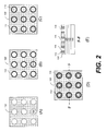
- FIG. 2 is a process flow for contact hole formation which is generally as discussed above with reference to FIG. 1 .
- FIG. 2A is a top-down view of the substrate following patterning and hardbake of the first photosensitive layer and post-exposure bake to form resist pattern 106' having contact hole patterns.
- FIG. 2B shows the substrate following alkaline surface treatment to form alkaline surface 112.
- FIG. 2C shows the substrate after formation of the second photosensitive layer 114.
- the substrate after second photosensitive soft-bake, flood-exposure and development is shown in FIG. 2D.
- FIG. 2E is a cross-sectional view taken along dashed line F-F in FIG. 2E .
- the softbake causes diffusion of the alkaline material to form alkaline region 112'.
- the contact hole opening becomes smaller as compared with the original contact pattern due to poisoning of the second resist layer in region 112'.
- the first photosensitive composition used to form resist pattern 106' has a higher characteristic post-exposure bake temperature than that of the second photosensitive composition used for second photosensitive layer 114.
- the critical dimension of the contact holes becomes reduced as a result of the poisoned regions 112' in the contact.
- the resist pattern 106' is not removed due to its higher characteristic post-exposure bake temperature than that used following exposure of the second photosensitive layer.
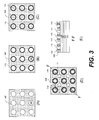
- FIG. 3 illustrates a process flow for a contact hole pitch-splitting process in accordance with the invention in which interstitial contact holes 117 are formed.
- the process for FIG. 3A-C is the same as that described above with respect to FIG. 2A-C , including first photosensitive patterning, second photosensitive layer coating, flood-exposure, post-exposure bake and development.
- the higher post-exposure bake temperature characteristic of the first resist pattern is used after the flood-exposure.
- the original contact holes 116 shrink and interstitial contact holes 117 can be formed, as shown in FIG. 3D-E .
- Interstitial holes typically result for higher density patterns of resist pattern contact holes, for example, 76nm diameter/140nm pitch holes.
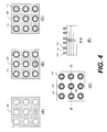
- FIG. 4 illustrates a process flow for a process which can be used to form donut shaped patterns 118.
- the process for FIG. 4A-C is the same as that described above with respect to FIG. 2A-C , including first photosensitive patterning, second photosensitive layer coating, flood-exposure, post-exposure bake and development.
- a post-exposure bake temperature higher than that characteristic of the first resist pattern is used after the flood-exposure.
- the original contact holes 116 shrink and the first resist pattern 106' can be removed as shown in FIG. 4D-E , resulting in donut-shaped patterns 118.
- Donut-shaped patterns are typically formed with semi-dense or isolated contact holes, for example, 88nm diameter/250nm pitch and 84nm diameter/700nm pitch holes.
- the methods of the invention can also be used to form pillar-shaped patterns.
- This process is generally the same as that described above with respect to FIG. 4 , except process conditions are selected such that the second photosensitive layer 114 becomes completely poisoned by the alkaline material. This can be accomplished, for example, by applying an increased amount of the alkaline material in the alkaline treatment process and/or by using a higher second photosensitive layer softbake temperature. In this way, the second photosensitive layer would not be removed following flood-exposure and development.
- Example 1 Contact Shrink Process Assisted by Double Exposure (SPADE) L1 Resist Polymer (Poly(IAM / ⁇ -GBLMA / ODOTMA / HAMA)) Synthesis
- a 500 ml flask equipped with a condenser, nitrogen inlet and mechanical stirrer was charged with 11 g of THF, and the solution was brought to a temperature of 67°C.
- 5.23g of dimethyl-2,2-azodiisobutyrate (17 mol% based on total monomers) was dissolved in 5g of THF and charged into the flask.
- the monomer solution was fed into a reactor at a rate of 16.0 milliliters per hour (mL/h) for 3 hours 30 minutes.
- the polymerization mixture was then stirred for an additional 30 minutes at 67°C.
- 5g of THF was next added to the reactor and the polymerization mixture was cooled to room temperature.
- a surface treatment solution was prepared by adding 0.0 1 g of (TAEA) (Sigma-Aldrich) to 99.99g of a surfactant solution (OptiPattern TM Clear-I, Air Products and Chemicals, Inc., Allentown, PA, USA). The resulting solution was filtered through a nylon filter having a 0.1 micron pore size.
- a 300 mm silicon wafer was spin-coated with ARTM40A antireflectant (Rohm and Haas Electronic Materials) to form a first bottom antireflective coating (BARC) on a TEL CLEAN TRACKTM LITHIUSTM i+ coater/developer.
- the wafer was baked for 60 seconds at 215°C, yielding a first BARC film thickness of 75nm.
- a second BARC layer was next coated over the first BARC using ARTM124 antireflectant (Rohm and Haas Electronic Materials), and was baked at 205°C for 60 seconds to generate a 23nm top BARC layer.
- the L1 resist formulation was coated on top of the dual BARCs and soft-baked at 110°C for 60 seconds with the coater/developer, resulting in a resist film thickness of 1000 ⁇ .
- the first resist layer was coated with a topcoat layer (OCTM2000 topcoat material, Rohm and Haas Electronic Materials) and exposed at various doses from 12.5 to 87.5 mJ/cm 2 through a binary reticle having contact hole patterns with various CDs and pitches using an ASML TWINSCANTM XT:1900i immersion scanner with a numerical aperture of 1.35 and annular illumination (0.8 outer sigma / 0.6 inner sigma) with XY-polarization.
- the wafer was then post-exposure baked (PEB) at 100°C for 60 seconds and developed for 12 seconds using MicropositTM MF CD-26 developer (Rohm and Haas Electronic Materials) to render contact hole (C/H) patterns with various CDs at different pitches.
- a full focus exposure matrix (FEM) of the C/H images was obtained by changing focus offset through X-direction and exposure dose through Y-direction.
- the C/H diameter was measured with a Hitachi CG 4000 SEM, with the results being shown in Table 1.
- the wafer was hardbaked at 180°C for 60 seconds.
- the wafer was next exposed to surface treatment chemistry in a sequential process by which the wafer was first rinsed with 2.38 wt% TMAH in water solution for 12 seconds using a TEL GP nozzle, and then rinsed with the surface treatment solution formulation.
- EPIC TM 2098 photoresist (Rohm and Haas Electronic Materials) was coated on the wafer containing the surface-treated contact hole patterns at a spin speed that would provide a film thickness of 650 ⁇ on a bare silicon wafer.
- the wafer was soft-baked at 120°C for 60 seconds on a the coater/developer.
- the wafer was then coated with OCTM 2000 topcoat material (Rohm and Haas Electronic Materials), and exposed using the same scanner settings as in the first lithographic process but using flood exposure and no mask at exposure doses of 28.7mJ/cm 2 , 20.5mJ/cm 2 and 12.3mJ/cm 2 at a fixed focus.
- the wafers were then post-exposure baked (PEB) at 90°C for 60 seconds and developed for 12 seconds using MicropositTM MF CD-26 developer (Rohm and Haas Electronic Materials).
- the contact hole diameter was again measured, with the results being shown below in Table 1. It was found that contact hole patterns having reduced CD as compared with the original patterns resulted from CD growth on the L1 resist patterns. Additionally, greater shrinkage of contact holes was obtained with a decrease in second (L2) resist exposure dose.
- a surface treatment solution was prepared by adding 2.5 g of a 1 wt% solution of TAEA in deionized water and 0.5 g of a 10% solution of TergitolTM TMN-6 in deionized water to 97 g of deionized water. The solution was filtered through a nylon filter having a 0.1 micron pore size.
- a 300 mm silicon wafer was spin-coated with ARTM40A antireflectant (Rohm and Haas Electronic Materials) to form a first bottom antireflective coating (BARC) on a TEL CLEAN TRACKTM LITHIUSTM i+ coater/developer.
- the wafer was baked for 60 seconds at 215°C, yielding a first BARC film thickness of 75nm.
- a second BARC layer was next coated over the first BARC using ARTM124 antireflectant (Rohm and Haas Electronic Materials), and was baked at 205°C for 60 seconds to generate a 23nm top BARC layer.
- An L1 photoresist composition as described in Example 1 was coated on top of the dual BARCs and soft-baked at 110°C for 60 seconds, resulting in a resist film thickness of 1000 ⁇ .
- the first resist layer was coated with a topcoat layer (OCTM2000 topcoat material, Rohm and Haas Electronic Materials) and exposed at various doses from 16 to 46 mJ/cm 2 through a binary reticle having various critical dimensions using an ASML TWINSCANTM XT:1900i immersion scanner with a numerical aperture of 1.35 and annular illumination (0.8 outer sigma/0.6 inner sigma) with XY-polarization.
- the wafer was then post-exposure baked (PEB) at 100°C for 60 seconds and developed for 12 seconds using MicropositTM MF CD-26 developer (Rohm and Haas Electronic Materials) to render first lithography (L1) patterns.
- the CD was measured with a Hitachi CG 4000 SEM and the mask CD used in this measurement was 76nm holes at 140nm pitch to give 78.8nm hole CD at 37 mJ/cm 2 .
- the wafer was hardbaked at 180°C for 60 seconds.
- the wafer was next surface treated in a sequential process by which the wafer was first rinsed with 2.38 wt% TMAH in water solution for 12 seconds using a TEL GP nozzle with rotation, and then rinsed with the surface treatment solution formulation described above.
- EPIC TM 2098 positive photoresist (Rohm and Haas Electronic Materials) was coated over the surface-treated L1 patterns on the coater/developer at a spin speed that would provide a film thickness of 650 ⁇ on a bare silicon wafer.
- the wafer was soft-baked at 120°C for 60 seconds, and then coated with OCTM 2000 topcoat material (Rohm and Haas Electronic Materials).
- the second lithography (L2) was carried out using the same scanner settings as in the first lithographic process but using flood exposure with no mask at 21 mJ/cm 2 .
- the wafer was then post-exposure baked at three temperatures (90, 100, and 110°C) for 60 seconds and developed for 12 seconds using MicropositTM MF CD-26 developer (Rohm and Haas Electronic Materials).
- the changes in the original contact hole CD of 90nm were measured with a Hitachi CG 4000 SEM. It was found that when higher a PEB temperature (110°C) was used in the L2 process, interstitial holes were formed between the original L1 contact holes such as shown in FIG. 3 .
- the original contact holes were also shrunk in this process when a lower L2 PEB temperature (90 and 100°C) was used.
Landscapes
- Physics & Mathematics (AREA)
- General Physics & Mathematics (AREA)
- Engineering & Computer Science (AREA)
- Condensed Matter Physics & Semiconductors (AREA)
- Computer Hardware Design (AREA)
- Microelectronics & Electronic Packaging (AREA)
- Power Engineering (AREA)
- Manufacturing & Machinery (AREA)
- Chemical & Material Sciences (AREA)
- Ceramic Engineering (AREA)
- Chemical Kinetics & Catalysis (AREA)
- Inorganic Chemistry (AREA)
- Organic Chemistry (AREA)
- Spectroscopy & Molecular Physics (AREA)
- Photosensitive Polymer And Photoresist Processing (AREA)
- Materials For Photolithography (AREA)
- Exposure Of Semiconductors, Excluding Electron Or Ion Beam Exposure (AREA)
- Exposure And Positioning Against Photoresist Photosensitive Materials (AREA)
- Drying Of Semiconductors (AREA)
Applications Claiming Priority (2)
| Application Number | Priority Date | Filing Date | Title |
|---|---|---|---|
| US26960009P | 2009-06-26 | 2009-06-26 | |
| US28168109P | 2009-11-19 | 2009-11-19 |
Publications (1)
| Publication Number | Publication Date |
|---|---|
| EP2287668A1 true EP2287668A1 (en) | 2011-02-23 |
Family
ID=42711855
Family Applications (3)
| Application Number | Title | Priority Date | Filing Date |
|---|---|---|---|
| EP10167367A Withdrawn EP2287668A1 (en) | 2009-06-26 | 2010-06-25 | Methods of forming electronic devices |
| EP10167369A Withdrawn EP2287669A1 (en) | 2009-06-26 | 2010-06-25 | Methods of forming electronic devices |
| EP10167371A Withdrawn EP2287670A1 (en) | 2009-06-26 | 2010-06-25 | Methods of forming electronic devices |
Family Applications After (2)
| Application Number | Title | Priority Date | Filing Date |
|---|---|---|---|
| EP10167369A Withdrawn EP2287669A1 (en) | 2009-06-26 | 2010-06-25 | Methods of forming electronic devices |
| EP10167371A Withdrawn EP2287670A1 (en) | 2009-06-26 | 2010-06-25 | Methods of forming electronic devices |
Country Status (6)
| Country | Link |
|---|---|
| US (7) | US8338083B2 (enExample) |
| EP (3) | EP2287668A1 (enExample) |
| JP (5) | JP5698922B2 (enExample) |
| KR (5) | KR101698396B1 (enExample) |
| CN (3) | CN101963754B (enExample) |
| TW (3) | TWI449084B (enExample) |
Cited By (1)
| Publication number | Priority date | Publication date | Assignee | Title |
|---|---|---|---|---|
| WO2014035871A1 (en) * | 2012-08-27 | 2014-03-06 | Tokyo Electron Limited | Euv resist sensitivity reduction |
Families Citing this family (56)
| Publication number | Priority date | Publication date | Assignee | Title |
|---|---|---|---|---|
| JP5698923B2 (ja) * | 2009-06-26 | 2015-04-08 | ローム・アンド・ハース・エレクトロニック・マテリアルズ,エル.エル.シー. | 自己整合型スペーサー多重パターニング方法 |
| JP5698922B2 (ja) * | 2009-06-26 | 2015-04-08 | ローム・アンド・ハース・エレクトロニック・マテリアルズ,エル.エル.シー. | 電子デバイスを形成する方法 |
| EP2336824A1 (en) | 2009-11-19 | 2011-06-22 | Rohm and Haas Electronic Materials, L.L.C. | Methods of forming electronic devices |
| JP5542500B2 (ja) * | 2010-03-30 | 2014-07-09 | 東京応化工業株式会社 | レジストパターン形成方法およびレジスト組成物 |
| KR20120027989A (ko) * | 2010-09-14 | 2012-03-22 | 삼성전자주식회사 | 반도체 소자의 패턴 형성방법 |
| KR101865296B1 (ko) * | 2011-06-15 | 2018-06-07 | 삼성전자주식회사 | 반도체 장치의 제조 방법 |
| CN102856190B (zh) * | 2011-06-30 | 2015-04-01 | 中芯国际集成电路制造(上海)有限公司 | 条形结构的刻蚀方法 |
| KR101909567B1 (ko) * | 2011-07-08 | 2018-10-18 | 에이에스엠엘 네델란즈 비.브이. | 리소그래피 패터닝 공정 및 상기 공정에 사용하기 위한 레지스트 |
| US9064808B2 (en) | 2011-07-25 | 2015-06-23 | Synopsys, Inc. | Integrated circuit devices having features with reduced edge curvature and methods for manufacturing the same |
| US8609550B2 (en) * | 2011-09-08 | 2013-12-17 | Synopsys, Inc. | Methods for manufacturing integrated circuit devices having features with reduced edge curvature |
| CN103034048B (zh) * | 2011-09-29 | 2015-04-22 | 中芯国际集成电路制造(北京)有限公司 | 光刻方法 |
| CN102364389A (zh) * | 2011-10-17 | 2012-02-29 | 深圳市华星光电技术有限公司 | 控制液晶显示装置接触孔孔壁角度的制作方法 |
| CN102437018B (zh) * | 2011-11-02 | 2017-11-24 | 上海华虹宏力半导体制造有限公司 | 用于改进蚀刻后晶圆内关键尺寸均匀性的烘烤方法及设备 |
| US8604427B2 (en) * | 2012-02-02 | 2013-12-10 | Applied Materials Israel, Ltd. | Three-dimensional mapping using scanning electron microscope images |
| JP6028357B2 (ja) | 2012-03-22 | 2016-11-16 | ソニー株式会社 | ヘッドマウントディスプレイ及び手術システム |
| EP2875406A4 (en) * | 2012-07-16 | 2016-11-09 | Basf Se | COMPOSITION FOR MANUFACTURING INTEGRATED CIRCUIT ARRANGEMENTS, OPTICAL DEVICES, MICROMETERS AND MECHANICAL PRECISION DEVICES |
| CN102751238A (zh) * | 2012-07-27 | 2012-10-24 | 上海华力微电子有限公司 | 通孔优先铜互连制作方法 |
| CN102810510A (zh) * | 2012-09-11 | 2012-12-05 | 上海华力微电子有限公司 | 一种铜互连制作方法 |
| CN102832168A (zh) * | 2012-09-11 | 2012-12-19 | 上海华力微电子有限公司 | 一种沟槽优先铜互连制作方法 |
| CN103839783B (zh) * | 2012-11-21 | 2017-06-09 | 中芯国际集成电路制造(上海)有限公司 | 自对准双重图形的形成方法 |
| JP6119669B2 (ja) * | 2013-06-11 | 2017-04-26 | 信越化学工業株式会社 | 下層膜材料及びパターン形成方法 |
| DE102013108876B4 (de) | 2013-08-16 | 2022-08-18 | OSRAM Opto Semiconductors Gesellschaft mit beschränkter Haftung | Fotolithografisches Verfahren zur Herstellung einer Struktur in einem Strahlung emittierenden Halbleiterbauelement |
| CN104425225A (zh) * | 2013-09-04 | 2015-03-18 | 中芯国际集成电路制造(上海)有限公司 | 三重图形的形成方法 |
| JP6340304B2 (ja) * | 2013-11-29 | 2018-06-06 | 富士フイルム株式会社 | パターン形成方法、及び電子デバイスの製造方法 |
| US9793268B2 (en) | 2014-01-24 | 2017-10-17 | Taiwan Semiconductor Manufacturing Company, Ltd. | Method and structure for gap filling improvement |
| TWI653507B (zh) * | 2014-02-07 | 2019-03-11 | 比利時商愛美科公司 | 用於減低微影製程後線寬粗糙度之電漿方法 |
| KR20150136387A (ko) | 2014-05-27 | 2015-12-07 | 삼성전자주식회사 | 반도체 소자의 제조 방법 |
| US9715724B2 (en) | 2014-07-29 | 2017-07-25 | Applied Materials Israel Ltd. | Registration of CAD data with SEM images |
| KR102270752B1 (ko) | 2014-08-11 | 2021-07-01 | 삼성전자주식회사 | 반도체 소자의 미세 패턴 형성 방법 |
| TWI675258B (zh) * | 2014-09-26 | 2019-10-21 | 日商東京應化工業股份有限公司 | 光阻圖型形成方法、光阻圖型分離劑、分離圖型改善化劑、光阻圖型分離材料及分離圖型形成用之正型光阻劑組成物 |
| TWI632437B (zh) * | 2014-11-07 | 2018-08-11 | 羅門哈斯電子材料有限公司 | 用於形成凸紋影像的方法 |
| US9673059B2 (en) * | 2015-02-02 | 2017-06-06 | Tokyo Electron Limited | Method for increasing pattern density in self-aligned patterning integration schemes |
| US9754791B2 (en) * | 2015-02-07 | 2017-09-05 | Applied Materials, Inc. | Selective deposition utilizing masks and directional plasma treatment |
| KR102370616B1 (ko) * | 2015-02-09 | 2022-03-04 | 삼성전자주식회사 | 미세 패턴 형성 방법 |
| US9633847B2 (en) * | 2015-04-10 | 2017-04-25 | Tokyo Electron Limited | Using sub-resolution openings to aid in image reversal, directed self-assembly, and selective deposition |
| US10935889B2 (en) * | 2015-05-13 | 2021-03-02 | Tokyo Electron Limited | Extreme ultra-violet sensitivity reduction using shrink and growth method |
| US10061199B2 (en) * | 2015-06-24 | 2018-08-28 | Tokyo Electron Limited | Methods of forming a mask for substrate patterning |
| US9741586B2 (en) * | 2015-06-30 | 2017-08-22 | Taiwan Semiconductor Manufacturing Company, Ltd. | Method of fabricating package structures |
| US10162265B2 (en) * | 2015-12-09 | 2018-12-25 | Rohm And Haas Electronic Materials Llc | Pattern treatment methods |
| US10503070B2 (en) * | 2015-12-10 | 2019-12-10 | Taiwan Semiconductor Manufacturing Co., Ltd. | Photosensitive material and method of lithography |
| KR102515807B1 (ko) * | 2016-01-11 | 2023-03-31 | 삼성디스플레이 주식회사 | 표시 장치 및 이의 제조 방법 |
| JP6741471B2 (ja) * | 2016-05-17 | 2020-08-19 | 東京応化工業株式会社 | レジストパターン形成方法 |
| CN107703722B (zh) * | 2016-08-08 | 2020-12-15 | 中芯国际集成电路制造(上海)有限公司 | 图案化光阻的形成方法 |
| US10115594B1 (en) * | 2017-09-05 | 2018-10-30 | Nanya Technology Corporation | Method of forming fine island patterns of semiconductor devices |
| JP2019078812A (ja) * | 2017-10-20 | 2019-05-23 | メルク、パテント、ゲゼルシャフト、ミット、ベシュレンクテル、ハフツングMerck Patent GmbH | 高精細パターンの製造方法およびそれを用いた表示素子の製造方法 |
| JP2019078810A (ja) * | 2017-10-20 | 2019-05-23 | メルク、パテント、ゲゼルシャフト、ミット、ベシュレンクテル、ハフツングMerck Patent GmbH | 微細パターンの製造方法およびそれを用いた表示素子の製造方法 |
| US10410878B2 (en) | 2017-10-31 | 2019-09-10 | American Air Liquide, Inc. | Hydrofluorocarbons containing —NH2 functional group for 3D NAND and DRAM applications |
| CN107761663A (zh) * | 2017-11-08 | 2018-03-06 | 江苏科技大学 | 一种板桩码头结构及其施工方法 |
| KR102462051B1 (ko) * | 2018-01-05 | 2022-11-01 | 도쿄엘렉트론가부시키가이샤 | 진보된 콘택 홀 패터닝 방법 |
| US11139402B2 (en) | 2018-05-14 | 2021-10-05 | Synopsys, Inc. | Crystal orientation engineering to achieve consistent nanowire shapes |
| US11143953B2 (en) | 2019-03-21 | 2021-10-12 | International Business Machines Corporation | Protection of photomasks from 193nm radiation damage using thin coatings of ALD Al2O3 |
| US11264458B2 (en) | 2019-05-20 | 2022-03-01 | Synopsys, Inc. | Crystal orientation engineering to achieve consistent nanowire shapes |
| US11886121B2 (en) * | 2019-08-30 | 2024-01-30 | Taiwan Semiconductor Manufacturing Co., Ltd. | Method for forming patterned photoresist |
| KR102827769B1 (ko) * | 2020-03-30 | 2025-07-01 | 램 리써치 코포레이션 | 밀폐형 오버레이어 (hermetic overlayer) 에 의한 포지티브 톤 건식 현상 (positive tone dry development) 을 달성하기 위한 구조체 및 방법 |
| CN117916855A (zh) | 2021-08-25 | 2024-04-19 | 杰米纳蒂奥公司 | 用于形成高密度接触的抗蚀剂内工艺 |
| US20250132166A1 (en) * | 2021-08-25 | 2025-04-24 | Geminatio, Inc. | Generation of multiline etch substrates |
Citations (21)
| Publication number | Priority date | Publication date | Assignee | Title |
|---|---|---|---|---|
| US3474054A (en) | 1966-09-13 | 1969-10-21 | Permalac Corp The | Surface coating compositions containing pyridine salts or aromatic sulfonic acids |
| US4200729A (en) | 1978-05-22 | 1980-04-29 | King Industries, Inc | Curing amino resins with aromatic sulfonic acid oxa-azacyclopentane adducts |
| US4251665A (en) | 1978-05-22 | 1981-02-17 | King Industries, Inc. | Aromatic sulfonic acid oxa-azacyclopentane adducts |
| EP0164248B1 (en) | 1984-06-01 | 1991-10-09 | Rohm And Haas Company | Photosensitive coating compositions, thermally stable coatings prepared from them, and the use of such coatings in forming thermally stable polymer images |
| US5128232A (en) | 1989-05-22 | 1992-07-07 | Shiply Company Inc. | Photoresist composition with copolymer binder having a major proportion of phenolic units and a minor proportion of non-aromatic cyclic alcoholic units |
| US5187019A (en) | 1991-09-06 | 1993-02-16 | King Industries, Inc. | Latent catalysts |
| EP0232972B1 (en) | 1986-01-13 | 1993-09-08 | Rohm And Haas Company | Negative photoresist compositions and processes for preparing thermally stable, negative images using them |
| US6534243B1 (en) * | 2000-10-23 | 2003-03-18 | Advanced Micro Devices, Inc. | Chemical feature doubling process |
| WO2003077029A1 (en) | 2002-03-04 | 2003-09-18 | Shipley Company, Llc | Negative photoresists for short wavelength imaging |
| US20060246373A1 (en) | 2005-05-01 | 2006-11-02 | Rohm And Haas Electronic Materials Llc | Compositions and processes for immersion lithography |
| US7332616B2 (en) | 2003-10-08 | 2008-02-19 | Shin-Etsu Chemical Co., Ltd. | Polymerizable compound, polymer, positive-resist composition, and patterning process using the same |
| US20080063985A1 (en) * | 2006-09-12 | 2008-03-13 | Hynix Semiconductor Inc. | Method for forming fine pattern of semiconductor device |
| WO2008070060A2 (en) * | 2006-12-06 | 2008-06-12 | Fujifilm Electronic Materials U.S.A., Inc. | Device manufacturing process utilizing a double pattering process |
| US20080193872A1 (en) | 2006-10-30 | 2008-08-14 | Rohm And Haas Electronic Materials Llc | Compositions and processes for immersion lithography |
| EP1975718A2 (en) * | 2007-03-26 | 2008-10-01 | FUJIFILM Corporation | Surface-treating agent for pattern formation and pattern-forming method using the surface-treating agent |
| WO2008143301A1 (ja) * | 2007-05-23 | 2008-11-27 | Jsr Corporation | パターン形成方法及びそれに用いる樹脂組成物 |
| WO2009009095A1 (en) * | 2007-07-10 | 2009-01-15 | Advanced Micro Devices, Inc. | Spacer lithography |
| US20090053657A1 (en) * | 2007-08-22 | 2009-02-26 | Shin-Etsu Chemical Co., Ltd. | Patterning process and pattern surface coating composition |
| US20090117489A1 (en) | 2007-11-05 | 2009-05-07 | Rohm And Haas Electronics Materials Llc | Compositons and processes for immersion lithography |
| US20090149026A1 (en) * | 2007-12-06 | 2009-06-11 | Micron Technology, Inc. | Method for forming high density patterns |
| US20090155715A1 (en) * | 2007-12-13 | 2009-06-18 | International Business Machines Corporation | Photoresist compositions and method for multiple exposures with multiple layer resist systems |
Family Cites Families (59)
| Publication number | Priority date | Publication date | Assignee | Title |
|---|---|---|---|---|
| JPS5844715A (ja) * | 1981-09-11 | 1983-03-15 | Fujitsu Ltd | 微細パタ−ン形成方法 |
| EP0358358B1 (en) * | 1988-08-26 | 1994-11-30 | Nippon Oil And Fats Company, Limited | Pigment dispersing agent |
| US5100696A (en) * | 1989-07-10 | 1992-03-31 | Ncr Corporation | Magnetic thermal transfer ribbon |
| JP3340493B2 (ja) * | 1993-02-26 | 2002-11-05 | 沖電気工業株式会社 | パターン形成方法、位相シフト法用ホトマスクの形成方法 |
| US5656121A (en) * | 1994-08-19 | 1997-08-12 | Minnesota Mining And Manufacturing Company | Method of making multi-layer composites having a fluoropolymer layer |
| JP3444692B2 (ja) * | 1995-04-14 | 2003-09-08 | 沖電気工業株式会社 | パターン形成方法 |
| JPH09191007A (ja) * | 1996-01-11 | 1997-07-22 | Sumitomo Chem Co Ltd | フォトレジスト用剥離液 |
| JPH11214510A (ja) * | 1998-01-26 | 1999-08-06 | Toshiba Corp | 自己整合型パターン形成方法 |
| JPH11251214A (ja) * | 1998-02-27 | 1999-09-17 | Sharp Corp | タンタル薄膜回路素子の製造方法 |
| US6218085B1 (en) * | 1999-09-21 | 2001-04-17 | Lucent Technologies Inc. | Process for photoresist rework to avoid sodium incorporation |
| JP2001135565A (ja) * | 1999-11-08 | 2001-05-18 | Sony Corp | 半導体装置の製造方法 |
| TWI281101B (en) * | 2000-02-28 | 2007-05-11 | Mitsubishi Electric Corp | Developing process, process for forming pattern and process for preparing semiconductor device using same |
| JP4329216B2 (ja) * | 2000-03-31 | 2009-09-09 | Jsr株式会社 | レジストパターン縮小化材料及びそれを使用する微細レジストパターンの形成方法 |
| JP2002006512A (ja) * | 2000-06-20 | 2002-01-09 | Mitsubishi Electric Corp | 微細パターン形成方法、微細パターン形成用材料、およびこの微細パターン形成方法を用いた半導体装置の製造方法 |
| KR100546098B1 (ko) * | 2000-12-27 | 2006-01-24 | 주식회사 하이닉스반도체 | 열산 발생제를 포함하는 포토레지스트 조성물을 이용하여포토레지스트 패턴 폭 감소 현상을 개선하는 방법 |
| JP2002278053A (ja) * | 2001-03-16 | 2002-09-27 | Fuji Photo Film Co Ltd | ポジ型フォトレジスト組成物 |
| US7670556B2 (en) * | 2001-07-10 | 2010-03-02 | Wisconsin Alumni Research Foundation | Surface plasmon resonance imaging of micro-arrays |
| JP3878451B2 (ja) * | 2001-10-22 | 2007-02-07 | 富士フイルムホールディングス株式会社 | 感光性樹脂転写材料、画像形成方法、カラーフィルターとその製造方法、フォトマスクとその製造方法 |
| JP2003228179A (ja) * | 2002-01-31 | 2003-08-15 | Mitsubishi Gas Chem Co Inc | 銅配線基板向けアミン含有レジスト剥離液および剥離方法 |
| JP4041750B2 (ja) * | 2002-06-28 | 2008-01-30 | 富士フイルム株式会社 | 染料含有硬化性組成物、カラーフィルタ及びその製造方法 |
| JP3675434B2 (ja) * | 2002-10-10 | 2005-07-27 | 東京応化工業株式会社 | 微細パターンの形成方法 |
| US6740473B1 (en) * | 2002-11-28 | 2004-05-25 | United Microelectronics Corp. | Method for shrinking critical dimension of semiconductor devices |
| US6916594B2 (en) * | 2002-12-30 | 2005-07-12 | Hynix Semiconductor Inc. | Overcoating composition for photoresist and method for forming photoresist pattern using the same |
| KR101076623B1 (ko) * | 2003-07-17 | 2011-10-27 | 에이제토 엘렉토로닉 마티리알즈 가부시키가이샤 | 미세 패턴 형성 재료 및 이를 사용한 미세 패턴 형성방법 |
| JP4143023B2 (ja) * | 2003-11-21 | 2008-09-03 | 株式会社東芝 | パターン形成方法および半導体装置の製造方法 |
| US20060003271A1 (en) * | 2004-06-30 | 2006-01-05 | Clark Shan C | Basic supercritical solutions for quenching and developing photoresists |
| KR100560633B1 (ko) * | 2004-08-16 | 2006-03-17 | 삼성전자주식회사 | 커패시터 제조 방법 |
| KR100575001B1 (ko) * | 2004-12-10 | 2006-04-28 | 삼성전자주식회사 | 상호 결합 없는 이중 포토 리소그라피 방법 |
| DE102005037022A1 (de) * | 2005-06-28 | 2007-01-04 | Osram Opto Semiconductors Gmbh | Strahlungsemittierender optoelektronischer Halbleiterchip mit einer Diffusionsbarriere |
| JP2007010785A (ja) * | 2005-06-28 | 2007-01-18 | Fujifilm Holdings Corp | 永久パターン形成方法 |
| JP4830596B2 (ja) * | 2006-04-10 | 2011-12-07 | 凸版印刷株式会社 | レジストパターン形成用基板、レジストパターン形成方法およびパネル |
| WO2007148160A2 (en) * | 2006-06-20 | 2007-12-27 | Freescale Semiconductor, Inc. | Method of multi-layer lithography |
| US7568362B2 (en) * | 2006-10-16 | 2009-08-04 | Calibre International, Llc | Bean bag holder to be used to hold a can or bottle |
| KR100876783B1 (ko) * | 2007-01-05 | 2009-01-09 | 주식회사 하이닉스반도체 | 반도체 소자의 미세 패턴 형성 방법 |
| JP5270840B2 (ja) * | 2007-01-23 | 2013-08-21 | 東京応化工業株式会社 | パターン微細化用被覆形成剤及びそれを用いた微細パターンの形成方法 |
| CN100490059C (zh) * | 2007-03-21 | 2009-05-20 | 山东华光光电子有限公司 | 一种高亮度发光二极管芯片的制备方法 |
| JP2008268855A (ja) * | 2007-03-26 | 2008-11-06 | Fujifilm Corp | パターン形成用表面処理剤、及び該処理剤を用いたパターン形成方法 |
| JP4840255B2 (ja) * | 2007-05-29 | 2011-12-21 | Jsr株式会社 | パターン形成方法及びそれに用いる樹脂組成物 |
| JP2009053547A (ja) * | 2007-08-28 | 2009-03-12 | Tokyo Ohka Kogyo Co Ltd | パターン形成方法及び被覆膜形成用材料 |
| JP5013119B2 (ja) * | 2007-09-20 | 2012-08-29 | 信越化学工業株式会社 | パターン形成方法並びにこれに用いるレジスト材料 |
| US7838198B2 (en) * | 2007-12-13 | 2010-11-23 | International Business Machines Corporation | Photoresist compositions and method for multiple exposures with multiple layer resist systems |
| JP2009194207A (ja) * | 2008-02-15 | 2009-08-27 | Tokyo Electron Ltd | パターン形成方法、半導体装置の製造方法及び半導体装置の製造装置 |
| JP5154395B2 (ja) * | 2008-02-28 | 2013-02-27 | 東京エレクトロン株式会社 | 半導体装置の製造方法及びレジスト塗布・現像処理システム |
| EP2101217B1 (en) * | 2008-03-14 | 2011-05-11 | Shin-Etsu Chemical Co., Ltd. | Sulfonium salt-containing polymer, resist compositon, and patterning process |
| US20090253080A1 (en) * | 2008-04-02 | 2009-10-08 | Dammel Ralph R | Photoresist Image-Forming Process Using Double Patterning |
| US20090253078A1 (en) * | 2008-04-07 | 2009-10-08 | Sokudo Co., Ltd. | Double exposure lithography using low temperature oxide and uv cure process |
| WO2010042159A1 (en) * | 2008-10-06 | 2010-04-15 | Union Carbide Chemicals & Plastics Technology Llc | Methods of making cyclic, n-amino functional triamines |
| KR101523951B1 (ko) * | 2008-10-09 | 2015-06-02 | 삼성전자주식회사 | 반도체 소자의 미세 패턴 형성 방법 |
| JP5071688B2 (ja) * | 2009-02-18 | 2012-11-14 | 信越化学工業株式会社 | パターン形成方法及びレジスト変性用組成物 |
| KR20100117025A (ko) * | 2009-04-23 | 2010-11-02 | 스미또모 가가꾸 가부시키가이샤 | 포토레지스트 패턴 형성 방법 |
| JP5212245B2 (ja) * | 2009-04-23 | 2013-06-19 | 住友化学株式会社 | レジストパターンの製造方法 |
| JP5112380B2 (ja) * | 2009-04-24 | 2013-01-09 | 信越化学工業株式会社 | パターン形成方法 |
| TWI403520B (zh) * | 2009-05-25 | 2013-08-01 | Shinetsu Chemical Co | 光阻改質用組成物及圖案形成方法 |
| JP5545029B2 (ja) * | 2009-05-25 | 2014-07-09 | 信越化学工業株式会社 | レジスト変性用組成物及びパターン形成方法 |
| JP5573356B2 (ja) * | 2009-05-26 | 2014-08-20 | 信越化学工業株式会社 | レジスト材料及びパターン形成方法 |
| JP5698923B2 (ja) * | 2009-06-26 | 2015-04-08 | ローム・アンド・ハース・エレクトロニック・マテリアルズ,エル.エル.シー. | 自己整合型スペーサー多重パターニング方法 |
| JP5698922B2 (ja) | 2009-06-26 | 2015-04-08 | ローム・アンド・ハース・エレクトロニック・マテリアルズ,エル.エル.シー. | 電子デバイスを形成する方法 |
| JP2011022187A (ja) * | 2009-07-13 | 2011-02-03 | Konica Minolta Business Technologies Inc | 静電荷像現像用トナー、フルカラートナーキット、画像形成方法 |
| EP2336824A1 (en) | 2009-11-19 | 2011-06-22 | Rohm and Haas Electronic Materials, L.L.C. | Methods of forming electronic devices |
-
2010
- 2010-06-25 JP JP2010144950A patent/JP5698922B2/ja not_active Expired - Fee Related
- 2010-06-25 TW TW099120756A patent/TWI449084B/zh not_active IP Right Cessation
- 2010-06-25 JP JP2010145317A patent/JP5698925B2/ja not_active Expired - Fee Related
- 2010-06-25 CN CN2010102632008A patent/CN101963754B/zh not_active Expired - Fee Related
- 2010-06-25 EP EP10167367A patent/EP2287668A1/en not_active Withdrawn
- 2010-06-25 CN CN2010102568270A patent/CN101937838B/zh not_active Expired - Fee Related
- 2010-06-25 JP JP2010145284A patent/JP5698924B2/ja not_active Expired - Fee Related
- 2010-06-25 EP EP10167369A patent/EP2287669A1/en not_active Withdrawn
- 2010-06-25 TW TW99120755A patent/TWI474378B/zh not_active IP Right Cessation
- 2010-06-25 TW TW099120758A patent/TWI420571B/zh not_active IP Right Cessation
- 2010-06-25 JP JP2010145349A patent/JP5698926B2/ja not_active Expired - Fee Related
- 2010-06-25 CN CN201010272367.0A patent/CN101963756B/zh not_active Expired - Fee Related
- 2010-06-25 EP EP10167371A patent/EP2287670A1/en not_active Withdrawn
- 2010-06-25 JP JP2010145376A patent/JP5731764B2/ja active Active
- 2010-06-28 KR KR1020100061494A patent/KR101698396B1/ko not_active Expired - Fee Related
- 2010-06-28 US US12/825,157 patent/US8338083B2/en not_active Expired - Fee Related
- 2010-06-28 KR KR1020100061502A patent/KR101766289B1/ko not_active Expired - Fee Related
- 2010-06-28 KR KR1020100061499A patent/KR101698400B1/ko not_active Expired - Fee Related
- 2010-06-28 KR KR1020100061498A patent/KR101724384B1/ko not_active Expired - Fee Related
- 2010-06-28 US US12/825,096 patent/US8465901B2/en not_active Expired - Fee Related
- 2010-06-28 US US12/825,124 patent/US8338079B2/en not_active Expired - Fee Related
- 2010-06-28 US US12/825,170 patent/US8507185B2/en not_active Expired - Fee Related
- 2010-06-28 US US12/825,134 patent/US8492068B2/en not_active Expired - Fee Related
- 2010-06-28 US US12/825,150 patent/US8492075B2/en not_active Expired - Fee Related
- 2010-06-28 KR KR1020100061495A patent/KR101671289B1/ko not_active Expired - Fee Related
-
2012
- 2012-09-15 US US13/620,754 patent/US20130069246A1/en not_active Abandoned
Patent Citations (23)
| Publication number | Priority date | Publication date | Assignee | Title |
|---|---|---|---|---|
| US3474054A (en) | 1966-09-13 | 1969-10-21 | Permalac Corp The | Surface coating compositions containing pyridine salts or aromatic sulfonic acids |
| US4200729A (en) | 1978-05-22 | 1980-04-29 | King Industries, Inc | Curing amino resins with aromatic sulfonic acid oxa-azacyclopentane adducts |
| US4251665A (en) | 1978-05-22 | 1981-02-17 | King Industries, Inc. | Aromatic sulfonic acid oxa-azacyclopentane adducts |
| EP0164248B1 (en) | 1984-06-01 | 1991-10-09 | Rohm And Haas Company | Photosensitive coating compositions, thermally stable coatings prepared from them, and the use of such coatings in forming thermally stable polymer images |
| EP0232972B1 (en) | 1986-01-13 | 1993-09-08 | Rohm And Haas Company | Negative photoresist compositions and processes for preparing thermally stable, negative images using them |
| US5128232A (en) | 1989-05-22 | 1992-07-07 | Shiply Company Inc. | Photoresist composition with copolymer binder having a major proportion of phenolic units and a minor proportion of non-aromatic cyclic alcoholic units |
| US5187019A (en) | 1991-09-06 | 1993-02-16 | King Industries, Inc. | Latent catalysts |
| US6534243B1 (en) * | 2000-10-23 | 2003-03-18 | Advanced Micro Devices, Inc. | Chemical feature doubling process |
| WO2003077029A1 (en) | 2002-03-04 | 2003-09-18 | Shipley Company, Llc | Negative photoresists for short wavelength imaging |
| US7332616B2 (en) | 2003-10-08 | 2008-02-19 | Shin-Etsu Chemical Co., Ltd. | Polymerizable compound, polymer, positive-resist composition, and patterning process using the same |
| US20090123869A1 (en) | 2005-05-01 | 2009-05-14 | Rohm And Haas Electronic Materials Llc | Compositions and processes for immersion lithography |
| US20060246373A1 (en) | 2005-05-01 | 2006-11-02 | Rohm And Haas Electronic Materials Llc | Compositions and processes for immersion lithography |
| US20080063985A1 (en) * | 2006-09-12 | 2008-03-13 | Hynix Semiconductor Inc. | Method for forming fine pattern of semiconductor device |
| US20080193872A1 (en) | 2006-10-30 | 2008-08-14 | Rohm And Haas Electronic Materials Llc | Compositions and processes for immersion lithography |
| WO2008070060A2 (en) * | 2006-12-06 | 2008-06-12 | Fujifilm Electronic Materials U.S.A., Inc. | Device manufacturing process utilizing a double pattering process |
| US20080199814A1 (en) | 2006-12-06 | 2008-08-21 | Fujifilm Electronic Materials, U.S.A., Inc. | Device manufacturing process utilizing a double patterning process |
| EP1975718A2 (en) * | 2007-03-26 | 2008-10-01 | FUJIFILM Corporation | Surface-treating agent for pattern formation and pattern-forming method using the surface-treating agent |
| WO2008143301A1 (ja) * | 2007-05-23 | 2008-11-27 | Jsr Corporation | パターン形成方法及びそれに用いる樹脂組成物 |
| WO2009009095A1 (en) * | 2007-07-10 | 2009-01-15 | Advanced Micro Devices, Inc. | Spacer lithography |
| US20090053657A1 (en) * | 2007-08-22 | 2009-02-26 | Shin-Etsu Chemical Co., Ltd. | Patterning process and pattern surface coating composition |
| US20090117489A1 (en) | 2007-11-05 | 2009-05-07 | Rohm And Haas Electronics Materials Llc | Compositons and processes for immersion lithography |
| US20090149026A1 (en) * | 2007-12-06 | 2009-06-11 | Micron Technology, Inc. | Method for forming high density patterns |
| US20090155715A1 (en) * | 2007-12-13 | 2009-06-18 | International Business Machines Corporation | Photoresist compositions and method for multiple exposures with multiple layer resist systems |
Cited By (2)
| Publication number | Priority date | Publication date | Assignee | Title |
|---|---|---|---|---|
| WO2014035871A1 (en) * | 2012-08-27 | 2014-03-06 | Tokyo Electron Limited | Euv resist sensitivity reduction |
| US9086631B2 (en) | 2012-08-27 | 2015-07-21 | Tokyo Electron Limited | EUV resist sensitivity reduction |
Also Published As
Similar Documents
| Publication | Publication Date | Title |
|---|---|---|
| US8338083B2 (en) | Methods of forming electronic devices | |
| US8394571B2 (en) | Methods of forming electronic devices | |
| EP2287667B1 (en) | Self-aligned spacer multiple patterning methods |
Legal Events
| Date | Code | Title | Description |
|---|---|---|---|
| PUAI | Public reference made under article 153(3) epc to a published international application that has entered the european phase |
Free format text: ORIGINAL CODE: 0009012 |
|
| 17P | Request for examination filed |
Effective date: 20100625 |
|
| AK | Designated contracting states |
Kind code of ref document: A1 Designated state(s): AL AT BE BG CH CY CZ DE DK EE ES FI FR GB GR HR HU IE IS IT LI LT LU LV MC MK MT NL NO PL PT RO SE SI SK SM TR |
|
| AX | Request for extension of the european patent |
Extension state: BA ME RS |
|
| GRAP | Despatch of communication of intention to grant a patent |
Free format text: ORIGINAL CODE: EPIDOSNIGR1 |
|
| STAA | Information on the status of an ep patent application or granted ep patent |
Free format text: STATUS: THE APPLICATION IS DEEMED TO BE WITHDRAWN |
|
| 18D | Application deemed to be withdrawn |
Effective date: 20130416 |