EP2286992B1 - Leitende folie und durchsichtiges heizelement - Google Patents
Leitende folie und durchsichtiges heizelement Download PDFInfo
- Publication number
- EP2286992B1 EP2286992B1 EP09750512.7A EP09750512A EP2286992B1 EP 2286992 B1 EP2286992 B1 EP 2286992B1 EP 09750512 A EP09750512 A EP 09750512A EP 2286992 B1 EP2286992 B1 EP 2286992B1
- Authority
- EP
- European Patent Office
- Prior art keywords
- thin metal
- conductive film
- conductive
- metal wires
- arcs
- Prior art date
- Legal status (The legal status is an assumption and is not a legal conclusion. Google has not performed a legal analysis and makes no representation as to the accuracy of the status listed.)
- Not-in-force
Links
Images


Classifications
-
- H—ELECTRICITY
- H05—ELECTRIC TECHNIQUES NOT OTHERWISE PROVIDED FOR
- H05B—ELECTRIC HEATING; ELECTRIC LIGHT SOURCES NOT OTHERWISE PROVIDED FOR; CIRCUIT ARRANGEMENTS FOR ELECTRIC LIGHT SOURCES, IN GENERAL
- H05B3/00—Ohmic-resistance heating
- H05B3/84—Heating arrangements specially adapted for transparent or reflecting areas, e.g. for demisting or de-icing windows, mirrors or vehicle windshields
-
- G—PHYSICS
- G06—COMPUTING OR CALCULATING; COUNTING
- G06F—ELECTRIC DIGITAL DATA PROCESSING
- G06F2203/00—Indexing scheme relating to G06F3/00 - G06F3/048
- G06F2203/041—Indexing scheme relating to G06F3/041 - G06F3/045
- G06F2203/04112—Electrode mesh in capacitive digitiser: electrode for touch sensing is formed of a mesh of very fine, normally metallic, interconnected lines that are almost invisible to see. This provides a quite large but transparent electrode surface, without need for ITO or similar transparent conductive material
-
- H—ELECTRICITY
- H05—ELECTRIC TECHNIQUES NOT OTHERWISE PROVIDED FOR
- H05B—ELECTRIC HEATING; ELECTRIC LIGHT SOURCES NOT OTHERWISE PROVIDED FOR; CIRCUIT ARRANGEMENTS FOR ELECTRIC LIGHT SOURCES, IN GENERAL
- H05B2203/00—Aspects relating to Ohmic resistive heating covered by group H05B3/00
- H05B2203/002—Heaters using a particular layout for the resistive material or resistive elements
Definitions
- the present invention relates to a conductive film that can be used as a part of a defroster (defrosting device) or a window glass for a vehicle, as a heating sheet for heat generation by applying electric current, or as an electrode for a touch panel, an inorganic EL device, an organic EL device, or a solar cell, and to a transparent heating element containing the conductive film.
- a device described in Japanese Laid-Open Patent Publication No. 2005-197234 has recently been proposed as an electroluminescence device capable of large-area (e.g., 0.25 m 2 or more) light emission with high luminance and long lifetime.
- the illuminance of a vehicle light may be reduced due to the following causes:
- the structure described in Japanese Laid-Open Patent Publication No. 2007-026989 is obtained by attaching a heating element containing a transparent insulating sheet and a conductive pattern printed thereon to a formed lens using an in-mold method.
- the conductive pattern of the heating element is composed of a composition containing a noble metal powder and a solvent-soluble thermoplastic resin.
- the structure described in Japanese Laid-Open Patent Publication No. 10-289602 is obtained by attaching a heating element to a lens portion in the vehicle lamp.
- the lens portion is heated by applying an electric field to the heating element under a predetermined condition.
- the heating element comprises a transparent conductive film of ITO (Indium Tin Oxide), etc.
- Japanese Laid-Open Patent Publication No. 2006-190585 has been proposed as a dye-sensitized solar cell capable of reducing adverse effects of reflected electromagnetic waves without significant reduction of the power generation efficiency.
- Japanese Laid-Open Patent Publication No. 2004-221565 has disclosed a technology for limiting a thickening ratio of line intersections in a mesh to minimize PDP image quality deterioration due to moire or the like.
- JP 2000 114770 A discloses a conductive film having a pattern in which curves (arcs) of adjacent lines vary.
- the size of mesh opening s varies locally, some being shrunk and some being expanded.
- the transmittance of a shrunk area and an expanded area becomes lower and higher, respectively. As a consequence, areas illuminated by a back lighting show different brightness.
- one conductive wire may be arranged in a zigzag manner on a headlamp front cover or the like to form a long conductive line in view of obtaining a desired resistance value (e.g., about 40 ohm).
- a desired resistance value e.g., about 40 ohm.
- a potential difference may be disadvantageously generated between adjacent conductive line portions to cause migration.
- the transparent conductive film of ITO, etc. is used.
- the film cannot be formed on a curved surface of a formed body by a method other than vacuum sputtering methods.
- the heating element is disadvantageous in efficiency, cost, etc.
- the transparent conductive film is composed of a ceramic such as ITO, the film may be cracked when bent in an in-mold method. Therefore, the film can hardly be used in a vehicle light front cover or the like having the curved-surface body and the transparent heater though it can be used in a window glass with relatively less curved surface.
- the conventional heating elements are less versatile and exclusively used in a vehicle light front cover, a window glass, etc.
- a conductive portion has to be formed in view of light refraction and diffraction in the portion to prevent glare caused by a backlight, etc.
- the solar cell described in Japanese Laid-Open Patent Publication No. 2006-190585 utilizes a transparent conductive film of ITO, etc., thereby resulting in the same problems as Japanese Laid-Open Patent Publication No. 10-289602 . Also the electromagnetic-shielding film technology described in Japanese Laid-Open Patent Publication No. 2004-221565 still has room for improvement.
- an object of the present invention is to provide a conductive film and a transparent heating element usable as a heating sheet for heat generation by applying electric current, which can exhibit an improved heat generation efficiency, can prevent glare caused by a vehicle or outdoor light, and can be versatilely used in a vehicle light front cover, a window glass, etc.
- Another object of the present invention is to provide a conductive film that can be used as an electrode of a touch panel, an inorganic EL device, or an organic EL device to prevent glare or the like caused by a backlight.
- a further object of the present invention is to provide a conductive film that can be used as an electrode of a solar cell to shield electromagnetic waves and to lower the surface resistance without reduction of the power generation efficiency.
- the inventor has examined a conductive film according to a comparative example having a plurality of conductive portions and a plurality of opening portions, which provide mesh shapes in combination. Specifically, the conductive portions are formed in a straight line shape and are crossed to form the mesh shapes.
- the heating wire When the heating wire is arranged in a zigzag manner in the conventional structure, a potential difference is generated between the adjacent conductive line portions to cause migration disadvantageously.
- the conductive portions are formed in the mesh shapes, the adjacent conductive portions are intrinsically in the short circuit condition, and the migration is never a problem.
- the conductive portions can be composed of a thin metal wire or the like excellent in malleability and ductility, and therefore can be formed along a three-dimensional curved surface having a minimum curvature radius of 300 mm or less.
- the conductive film or the transparent heating element of the present invention when used as a heating sheet for heat generation by applying electric current, it can exhibit an improved heat generation efficiency, can prevent glare caused by a vehicle or outdoor light, and can be versatilely used in a vehicle light front cover, a window glass, etc.
- the conductive film of the present invention When the conductive film of the present invention is used as an electrode of a touch panel, an inorganic EL device, or an organic EL device, glare or the like caused by a backlight can be prevented.
- the conductive film of the present invention When used as an electrode of a solar cell, it can act as an electromagnetic-shielding film and can exhibit a low surface resistance to prevent reduction of the power generation efficiency.
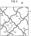
- a conductive film according to a first embodiment contains a plurality of conductive portions 12 and a plurality of opening portions 14, and the combination of the conductive portions 12 and the opening portions 14 has mesh shapes M.
- Each mesh shape M is a combined shape of one opening portion 14 and four conductive portions 12 surrounding the opening portion 14.
- the first conductive film 10A can be used as a part of a defroster (defrosting device) or a window glass for a vehicle.
- the first conductive film 10A can be used also in a transparent heating element capable of heat generation by applying electric current.
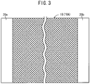
- the first conductive film 10A has a transparent film substrate 16, and the conductive portions 12 and the opening portions 14 formed thereon.
- a first electrode 20a and a second electrode 20b are disposed on the opposite ends of the first conductive film 10A (e.g., the right and left ends of FIG. 3 ).
- the transparent heating element 18 When an electric current is flowed from the first electrode 20a to the second electrode 20b, the transparent heating element 18 generates heat. Thus, a heating object (such as a building window glass, a vehicle window glass, or a vehicle light front cover), which is brought into contact or equipped with the transparent heating element 18, is heated. As a result, snow or the like attached to the object can be removed.
- a heating object such as a building window glass, a vehicle window glass, or a vehicle light front cover
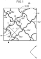
- the conductive portions 12 in the first conductive film 10A have a mesh pattern 22 formed by crossing a plurality of first thin metal wires 12a arranged at a first pitch L1 in one direction (the x direction of FIG. 1 ) and a plurality of second thin metal wires 12b arranged at a second pitch L2 in another direction (the y direction of FIG. 1 ).
- the first pitch L1 and the second pitch L2 may be selected within a range of 150 ⁇ m to 6000 ⁇ m (6.0 mm).
- the line width d of the first thin metal wires 12a and the second thin metal wires 12b may be selected within a range of 5 ⁇ m to 200 ⁇ m (0.2 mm). It is to be understood that the line width d may be selected within a range of 5 to 50 ⁇ m to improve the transparency.
- the conductive portions 12 are formed of the plural first thin metal wires 12a and the plural second thin metal wires 12b in the mesh pattern 22 having a large number of lattice intersection points (intersections 24).
- Each of the conductive portions 12 is formed in a wavy line shape containing at least one curve between the intersections 24.
- each alternate first thin metal wire 12a1 (one first thin metal wire 12a1) has a shape with arc-shaped curves, and two arcs 26 extending in alternate crest and trough directions are continuously formed between the intersections 24.
- each first thin metal wire 12a2 other than the first thin metal wires 12a1 (the other first thin metal wire 12a2) has a shape with arc-shaped curves, and four arcs 26 extending in alternate crest and trough directions are continuously formed between the intersections 24.
- the length, in which two arcs 26 extending in alternate crest and trough directions are continuously formed is considered as 1 period. Then, the one first thin metal wire 12a1 have 1 period of the arcs between the intersections, and the other first thin metal wires 12a2 have 2 periods of the arcs between the intersections.
- the adjacent parallel first thin metal wires 12a (the one first thin metal wire 12a1 and the other first thin metal wire 12a2) have different arc arrangement periods.
- one second thin metal wires 12b1 have 1 period of the arcs between the intersections 24, and the other second thin metal wires 12b2 have 2 periods of the arcs between the intersections 24.
- the periods may satisfy one of the following relations.
- Each arc 26 has a central angle of 75° to 105°, preferably approximately 90°.
- the conductive portions 12 have a crossing angle of approximately 90°. Though the preferred central angle and the preferred crossing angle are represented by the term "approximately 90°" in view of production tolerance, it is desired that the central angle and the crossing angle are ideally 90°.
- the 1 period is preferably 50 to 2000 ⁇ m.
- each conductive portion 12 has a constant amplitude h.
- the amplitude h is a distance from the crest to the intersection point of the perpendicular line and the imaginary line 28.
- the amplitude h is preferably 10 to 500 ⁇ m.
- adjacent two arcs 26 between the intersections 24 may have different amplitudes, and the adjacent parallel wavy line shapes may have different arc amplitudes.
- the length La of a first line segment connecting the central point of one mesh shape M1 and the intersection 24 is equal to the length Lb of a second line segment connecting the central point of the other mesh shape M2 and the intersection 24.
- the length Lc of a third line segment connecting the central point C3 of one mesh shape M3 and the first thin metal wire 12a is equal to the length Ld of a fourth line segment connecting the central point C4 of the other mesh shape M4 and the first thin metal wire 12a.
- the first conductive film 10A has a total light transmittance of 70% or more but less than 99%, which can be increased to 80% or more or 85% or more.
- the conductive portions 12 hardly have a straight section, so that diffraction points are not arranged linearly on the intersections 24 of the conductive portions 12.
- the adjacent parallel thin metal wires are formed in the wavy line shapes with different periods, whereby the diffraction points are discretely distributed to further reduce glare or the like caused by interference of diffracted lights.
- an interfering light from the intersections 24 has a low intensity
- an interfering light from the conductive portions 12 has a low intensity.
- the glare or the like caused by the interference of diffracted lights is thus prevented that would otherwise be caused by the mesh shapes.
- the opening portions 14 have approximately constant opening areas, whereby the glare or the like caused by the interference of diffracted lights can be prevented on the whole surface, and significant glare or the like is not caused locally.
- the first conductive film 10A is suitable for the transparent heating element 18, which can be incorporated in a window glass (such as a building window glass or a vehicle window glass), a vehicle light front cover, etc.
- the straight section may be appropriately formed in the wavy line shape if necessary depending on the product (such as the window glass or the vehicle light front cover), the period or amplitude of the wavy line shape, etc.
- the wavy line shape may be a sine wave curve shape.
- FIG. 5 is a front view showing the first conductive sheet 100
- FIG. 6 is a back view showing the first conductive sheet 100
- FIG. 7 is a top view showing the first conductive sheet 100
- FIG. 8 is a bottom view showing the first conductive sheet 100
- FIG. 9 is a left side view showing the first conductive sheet 100
- FIG. 10 is a right side view showing the first conductive sheet 100.
- FIG. 11 is a perspective view showing the first conductive sheet 100
- FIG. 12 is a front view showing the use of the first conductive sheet 100.
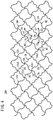
- the first conductive sheet 100 contains a transparent film substrate 16 and a wavy conductive pattern (conductive portions) 12 formed thereon.
- the design of the first conductive sheet 100 is continuously formed in the vertical and horizontal directions of the front view.
- the transparent film substrate 16 is colorless and clear, and the conductive pattern (conductive portions) 12 has a black color.
- the first conductive sheet 100 can be used as a part of a defroster (defrosting device) or a window glass for a vehicle, etc.
- the first conductive sheet 100 can be used also as a heating sheet capable of heat generation by applying electric current.
- the first conductive sheet 100 can be used as an electrode for a touch panel, an inorganic EL device, an organic EL device, or a solar cell.
- electrodes are disposed on the opposite ends of the first conductive sheet 100 (e.g., the right and left ends of FIG. 12 ), and an electric current is flowed from one electrode to the other electrode to heat the conductive pattern 12.
- the pitches of the conductive pattern 12 may be selected within a range of 0.1 to 6.0 mm (more preferably 0.3 to 6.0 mm). In this example, the dimensions L1 and L2 are the same value of about 5.8 mm.
- the line width of the conductive pattern 12 (the dimension d of FIG. 5 ) is about 0.1 mm in this example though it may be selected within a range of 0.01 to 0.2 mm.
- the thickness of the transparent film substrate 16 (the dimension t2 of FIG.
- the thickness of the conductive pattern 12 (the dimension t1 of FIG. 8 ) is about 0.1 mm in this example though it may be selected within a range of 0.001 to 0.2 mm.
- a conductive film according to a second embodiment (hereinafter referred to as the second conductive film 10B) will be described below with reference to FIG. 13 .
- the structure of the second conductive film 10B is approximately the same as that of the above first conductive film 10A, but different in the following respect.
- one first thin metal wire 12a1 is formed in a wavy line shape containing at least one curve (e.g., the arc 26) between the intersections 24, and the other first thin metal wire 12a2 is formed in a straight line shape.
- one second thin metal wire 12b1 is formed in a wavy line shape containing at least one curve (e.g., the arc 26) between the intersections 24, and the other second thin metal wire 12b2 is formed in a straight line shape.
- the wavy line shapes of the one first thin metal wire 12a1 and the one second thin metal wire 12b1 have 1 period of the arcs 26 between the intersections 24.
- first and second electrodes are disposed on the opposite ends of the second conductive film 10B.
- the transparent heating element 18 generates heat.
- the second conductive film 10B is suitable for the transparent heating element 18 that can be incorporated in a window glass (such as a building window glass or a vehicle window glass), a vehicle light front cover, etc.
- the pitches may be increased or decreased locally.
- the opening areas of the opening portions 14 may be locally changed.
- a local portion having a decreased pitch exhibits higher heat generation efficiency
- a local portion having an increased pitch exhibits a higher light transmittance.
- the pitches may be selected in each portion of the window glass such as a portion requiring rapid snow melting or a portion requiring transparency.
- the transparent heating element 18 when used in a vehicle window glass (a front window glass), the rapid snow melting, the transparency, and a longer current pathway are required in a portion facing a driver, so that it is preferred that the local portion with an increased pitch and the local portion with a decreased pitch are arranged in combination.
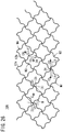
- a conductive film according to a third embodiment (hereinafter referred to as the third conductive film 10C) will be described below with reference to FIG. 14 .
- the structure of the third conductive film 10C is approximately the same as that of the above first conductive film 10A, but different in the following respect.
- a number-one first thin metal wire 12a(1) has a smallest arrangement period number of the arcs 26 (a largest length of the arrangement period of the arcs 26), and the arrangement period number of the arcs 26 is increased stepwise (the length of the arc arrangement period is reduced stepwise) from the number-one first thin metal wire 12a(1) to another first thin metal wire 12a arranged in one direction.
- the arrangement period number of the arcs 26 is increased stepwise (the length of the arc arrangement period is reduced stepwise) from the number-one first thin metal wire 12a(1) to another first thin metal wire 12a arranged in one direction.
- the number-one first thin metal wire 12a(1) has an arc arrangement period number of 1
- the number-two first thin metal wire 12a(2) adjacent to the number-one first thin metal wire 12a(1) in the one direction has an arc arrangement period number of 2
- the number-three first thin metal wire 12a(3) adjacent to the number-two first thin metal wire 12a(2) in the one direction has an arc arrangement period number of 3.
- the combinations of the wires are arranged in the one direction.
- the first thin metal wire 12a adjacent to the number-one first thin metal wire 12a(1) in the opposite direction has an arc arrangement period number of 3. Therefore, the first thin metal wire 12a having the largest arc arrangement period number is adjacent to the first thin metal wire 12a having the smallest arc arrangement period number.
- the second thin metal wires 12b are arranged in the same manner.
- the conductive portions 12 hardly have a straight section, so that diffraction points are not arranged linearly on the intersections 24 of the conductive portions 12.
- the adjacent parallel thin metal wires 12 are formed in the wavy line shapes with different periods, whereby the diffraction points are discretely distributed to further reduce the glare or the like caused by the interference of diffracted lights.
- FIG. 15 is a front view showing the second conductive sheet 200
- FIG. 16 is a back view showing the second conductive sheet 200
- FIG. 17 is a top view showing the second conductive sheet 200
- FIG. 18 is a bottom view showing the second conductive sheet 200
- FIG. 19 is a left side view showing the second conductive sheet 200
- FIG. 20 is a right side view showing the second conductive sheet 200.
- FIG. 21 is a perspective view showing the second conductive sheet 200
- FIG. 22 is a front view showing the use of the second conductive sheet 200.
- the second conductive sheet 200 contains a transparent film substrate 16 and a wavy conductive pattern (conductive portions) 12 formed thereon.
- the design of the second conductive sheet 200 is continuously formed in the vertical and horizontal directions of the front view.
- the transparent film substrate 16 is colorless and clear, and the conductive pattern (conductive portions) 12 has a black color.
- the second conductive sheet 200 can be used as a part of a defroster (defrosting device) or a window glass for a vehicle, etc.
- the second conductive sheet 200 can be used also as a heating sheet capable of heat generation by applying electric current.
- the second conductive sheet 200 can be used as an electrode for a touch panel, an inorganic EL device, an organic EL device, or a solar cell.
- electrodes are disposed on the opposite ends of the second conductive sheet 200 (e.g., the right and left ends of FIG. 22 ), and an electric current is flowed from one electrode to the other electrode to heat the conductive pattern 12.
- the pitches of the conductive pattern 12 may be selected within a range of 0.15 to 6.0 mm. In this example, the dimensions L1 and L2 are the same value of about 5.8 mm.
- the line width of the conductive pattern 12 (the dimension d of FIG. 15 ) is about 0.1 mm in this example though it may be selected within a range of 0.01 to 0.2 mm.
- the thickness of the transparent film substrate 16 (the dimension t2 of FIG.
- the thickness of the conductive pattern 12 (the dimension t1 of FIG. 18 ) is about 0.1 mm in this example though it may be selected within a range of 0.001 to 0.2 mm.
- a conductive film according to a fourth embodiment (hereinafter referred to as the fourth conductive film 10D) will be described below with reference to FIG. 23 .
- the structure of the fourth conductive film 10D is approximately the same as that of the above third conductive film 10C, but different in the following respect.
- first thin metal wires 12a two first thin metal wires 12a disposed adjacently on either side of a first thin metal wire 12a having a smallest arc arrangement period number (a largest arc arrangement period length) have the same arc arrangement period number, and two first thin metal wires 12a disposed adjacently on either side of a first thin metal wire 12a having a largest arc arrangement period number (a smallest arc arrangement period length) have the same arc arrangement period number.
- the second thin metal wires 12b are formed in the same manner.
- the conductive portions 12 hardly have a straight section, so that diffraction points are not arranged linearly on the intersections 24 of the conductive portions 12.
- the adjacent parallel thin metal wires 12 are formed in the wavy line shapes with different periods, whereby the diffraction points are discretely distributed to further reduce the glare or the like caused by the interference of diffracted lights.
- the pattern of the first thin metal wires 12a may be arranged such that, calling one first thin metal wire 12a having a smallest arc arrangement period number a number-one first thin metal wire 12a, the arc arrangement period number of the first thin metal wire 12a is increased stepwise from the number-one first thin metal wire 12a in one direction in the same manner as in the third conductive film 10C, and the pattern of the second thin metal wires 12b may be arranged such that two second thin metal wires 12b disposed adjacently on either side of a second thin metal wire 12b having a smallest arc arrangement period number have the same arc arrangement period number and two second thin metal wires 12b disposed adjacently on either side of a second thin metal wire 12b having a largest arc arrangement period number have the same arc arrangement period number in the same manner as in the fourth conductive film 10D.
- the first thin metal wires 12a may be patterned in the same manner as in the fourth conductive film 10D, and the
- a conductive film according to a fifth embodiment (hereinafter referred to as the fifth conductive film 10E) will be described below with reference to FIG. 24 .
- the structure of the fifth conductive film 10E is approximately the same as that of the above first conductive film 10A, but different in the following respect.
- the conductive portions 12 have a wavy line shape with a constant period.
- 1 period of the arcs are arranged between the intersections 24.
- the first line segment length La is equal to the second line segment length Lb
- the third line segment length Lc is equal to the fourth line segment length Ld, as in the first conductive film 10A.
- a pair of optional tangent lines which are positioned on the circumference line of each mesh shape M symmetrically about the central point C of the mesh shape M, are parallel to each other.
- a pair of first tangent lines (1)(1), a pair of second tangent lines (2)(2), and a pair of third tangent lines (3)(3) are parallel to each other, respectively, and have different tangent directions.
- a light is highly refracted and diffracted in a tangent direction.
- a light can be refracted and diffracted in a large number of the different tangent directions to reduce the significant glare.
- the opening portions 14 have approximately constant opening areas, whereby the glare or the like caused by the interference of diffracted lights can be prevented on the whole surface, and the significant glare or the like is not caused locally.
- the fifth conductive film 10E is capable of improving heat generation efficiency in a transparent heating element and improving power generation efficiency in a solar cell.
- a conductive film according to a sixth embodiment (hereinafter referred to as the sixth conductive film 10F) will be described below with reference to FIG. 25 .
- the structure of the sixth conductive film 10F is approximately the same as that of the above fifth conductive film 10E.
- the first line segment length La is equal to the second line segment length Lb as in the fifth conductive film 10E.
- a pair of optional tangent lines which are positioned on the circumference line of each mesh shape M symmetrically about the central point C of the mesh shape M, are parallel to each other.
- the length Lc of a third line segment connecting the central point C3 of one mesh shape M3 and the first thin metal wire 12a is different from the length Ld of a fourth line segment connecting the central point C4 of the other mesh shape M4 and the first thin metal wire 12a.
- the length Lc is larger than the length Ld. It should be noted that the intersections 24 are at a distance of 0.5 periods in this example.
- a light can be refracted and diffracted in a large number of the different tangent directions to reduce the significant glare.
- the opening portions 14 have approximately constant opening areas, whereby the glare or the like caused by the interference of diffracted lights can be prevented on the whole surface, and the significant glare or the like is not caused locally.
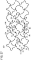
- a conductive film according to a seventh embodiment (hereinafter referred to as the seventh conductive film 10G) will be described below with reference to FIG. 26 .
- the structure of the seventh conductive film 10G is approximately the same as that of the above sixth conductive film 10F.
- the distance La is equal to the distance Lb
- the distance Lc is different from the distance Ld
- a pair of optional tangent lines which are positioned on the circumference line of each mesh shape M symmetrically about the central point C of the mesh shape M, are parallel to each other.
- the seventh conductive film 10G is different from the sixth conductive film 10F in that 1.5 periods of the arcs are arranged between the intersections 24.
- a light can be refracted and diffracted in a large number of different directions to reduce the significant glare.
- the opening portions 14 have approximately constant opening areas, whereby the glare or the like caused by the interference of diffracted lights can be prevented on the whole surface, and the significant glare or the like is not caused locally.
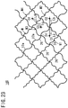
- a conductive film according to an eighth embodiment (hereinafter referred to as the eighth conductive film 10H) will be described below with reference to FIG. 27 .
- the structure of the eighth conductive film 10H is approximately the same as that of the above sixth conductive film 10F.
- the distance La is equal to the distance Lb
- the distance Lc is different from the distance Ld
- a pair of optional tangent lines which are positioned on the circumference line of each mesh shape M symmetrically about the central point C of the mesh shape M, are parallel to each other.
- the eighth conductive film 10H is different from the sixth conductive film 10F in that the arc arrangement period between one intersection 24 and a first intersection 24a adjacently disposed at one side of the one intersection 24 along the extending direction of the first thin metal wire 12a is different from the arc arrangement period between the one intersection 24 and a second intersection 24b adjacently disposed at the other side of the one intersection 24.
- the one intersection 24 and the first intersection 24a are at a distance of 0.5 periods
- the one intersection 24 and the second intersection 24b are at a distance of 1.5 periods.
- the arc arrangement period between the one intersection 24 and a third intersection 24c adjacently disposed at one side of the one intersection 24 along the extending direction of the second thin metal wire 12b is different from the arc arrangement period between the one intersection 24 and a fourth intersection 24d adjacently disposed at the other side of the one intersection 24.
- the one intersection 24 and the third intersection 24c are at a distance of 1.5 periods
- the one intersection 24 and the fourth intersection 24d are at a distance of 0.5 periods.
- a light can be refracted and diffracted in a large number of different directions to reduce the significant glare.
- the films 10E to 10H are capable of exhibiting a low overall surface resistance, improving heat generation efficiency in a transparent heating element, and improving power generation efficiency in a solar cell.
- a photosensitive silver salt layer is formed, exposed, developed, and fixed on the transparent film substrate 16 to form metallic silver portions.
- the metallic silver portions and a conductive metal disposed thereon are utilized for forming the mesh pattern 22.
- the transparent film substrate 16 is coated with a photosensitive silver salt layer 34 containing a mixture of a gelatin 33 and a silver halide 31 (e.g., silver bromide particles, silver chlorobromide particles, or silver iodobromide particles).
- a silver halide 31 e.g., silver bromide particles, silver chlorobromide particles, or silver iodobromide particles.
- the photosensitive silver salt layer 34 is subjected to an exposure treatment for forming the mesh pattern 22.
- an optical energy is applied to the silver halide 31, the silver halide 31 is exposed to generate invisible minute silver nuclei, referred to as a latent image.
- the photosensitive silver salt layer 34 is subjected to a development treatment for converting the latent image to an image visible to the naked eye.
- the photosensitive silver salt layer 34 having the latent image is developed using a developer, which is an alkaline or acidic solution, generally an alkaline solution.
- a developer which is an alkaline or acidic solution, generally an alkaline solution.
- silver ions from the silver halide particles or the developer are reduced to metallic silver by a reducing agent in the developer (referred to as a developing agent).
- a developing agent a reducing agent in the developer
- the photosensitive silver halide 31 remains in the photosensitive silver salt layer 34 after the development treatment. As shown in FIG. 28D , the silver halide 31 is removed by a fixation treatment using a fixer, which is an acidic or alkaline solution, generally an acidic solution.
- a fixer which is an acidic or alkaline solution, generally an acidic solution.
- metallic silver portions 36 are formed in exposed areas, and light-transmitting portions 38 containing only the gelatin 33 are formed in unexposed areas.
- the combination of the metallic silver portions 36 and the light-transmitting portions 38 is formed on the transparent film substrate 16.
- the silver thiosulfate complex has a high water solubility, and thereby is eluted from the gelatin 33. As a result, the developed silvers 35 are fixed and remain as the metallic silver portions 36.
- the latent image is reacted with the reducing agent to deposit the developed silvers 35 in the development treatment, and the residual silver halide 31, not converted to the developed silvers 35, is eluted into water in the fixation treatment.
- the treatments are described in detail in T. H. James, "The Theory of the Photographic Process, 4th ed.”, Macmillian Publishing Co., Inc., NY, Chapter 15, pp. 438-442, 1977 .
- the development treatment is generally carried out using the alkaline solution.
- the alkaline solution used in the development treatment may be mixed into the fixer (generally an acidic solution), whereby the activity of the fixer may be disadvantageously changed in the fixation treatment.
- the developer may remain on the film after removing the film from the development bath, whereby an undesired development reaction may be accelerated by the developer.
- a quencher such as an acetic acid solution after the development treatment before the fixation treatment.
- a conductive metal 40 may be disposed only on the metallic silver portions 36 by a plating treatment (such as an electroless plating treatment, an electroplating treatment, or a combination thereof), etc.
- the mesh pattern 22 is formed of the metallic silver portions 36 on the transparent film substrate 16 and the conductive metal 40 disposed on the metallic silver portions 36.
- a photopolymerization initiator absorbs a light in an exposure treatment to initiate a reaction, a photoresist film (a resin) per se undergoes a polymerization reaction to increase or decrease the solubility in a developer, and the resin in an exposed or unexposed area is removed in a development treatment.
- the developer liquid used in the resist technology may be an alkaline solution free of reducing agents, in which an unreacted resin component can be dissolved.
- the minute silver nuclei (the so-called latent image) are formed from the silver ion and a photoelectron generated in the silver halide 31 exposed in the exposure treatment.
- the latent image silver nuclei are grown to form the visible silver image in the development treatment using the developer, which must contain the reducing agent (the developing agent).
- the resist technology and the silver salt photography technology are greatly different in the reactions in the exposure and development treatments.
- the unpolymerized resin portion in the exposed or unexposed area is removed.
- the reduction reaction is conducted by the reducing agent contained in the developer (the developing agent), and the developed silver 35 is grown into a visible size.
- the gelatin 33 in the unexposed area is not removed.
- the silver halide 31 contained in the gelatin 33 in the unexposed area is eluted in the following fixation treatment, and the gelatin 33 is not removed.
- the main reaction component (the main photosensitive component) is the silver halide in the silver salt photography technology, while it is the photopolymerization initiator in the resist technology. Further, in the development treatment, the binder (the gelatin 33) remains in the silver salt photography technology, while it is removed in the resist technology.
- the resist technology and the silver salt photography technology are greatly different in these points.
- a mask used in the exposure treatment of the photosensitive silver salt layer 34 may have a mask pattern corresponding to the mesh pattern 22 of the conductive portions 12 having the wavy line shape containing at least one curve between the intersections 24.
- a photoresist film 44 is formed on a copper foil 42 disposed on the transparent film substrate 16, and the photoresist film 44 is exposed and developed to form a resist pattern 46.
- the copper foil 42 exposed from the resist pattern 46 is etched to form the mesh pattern 22.
- a mask used in the exposure treatment of the photoresist film 44 may have a mask pattern corresponding to the mesh pattern 22.
- a paste 48 containing fine metal particles is printed on the transparent film substrate 16.
- the printed paste 48 may be plated with a metal 50 to form the mesh pattern 22.
- the mesh pattern 22 may be printed on the transparent film substrate 16 by using a screen or gravure printing plate.
- a particularly preferred method of forming a thin conductive metal film using a photographic photosensitive silver halide material for the conductive film 10 of this embodiment will be mainly described below.
- the conductive film 10 of this embodiment may be produced as follows.
- a photosensitive material having the transparent film substrate 16 and thereon a photosensitive silver halide-containing emulsion layer is exposed and developed, whereby the metallic silver portions 36 and the light-transmitting portions 38 are formed in the exposed areas and the unexposed areas respectively.
- the metallic silver portions 36 may be subjected to a physical development treatment and/or a plating treatment to deposit the conductive metal 40 thereon.
- the method for forming the conductive film 10 of the embodiment includes the following three processes, depending on the photosensitive materials and development treatments.
- an integral black-and-white development procedure is used to form a transmittable conductive film such as an electromagnetic-shielding film or a light-transmitting conductive film on the photosensitive material.
- the resulting silver is a chemically or thermally developed silver containing a high-specific surface area filament, and thereby shows a high activity in the following plating or physical development treatment.
- the silver halide particles are melted around the physical development nuclei and deposited on the nuclei in the exposed areas, to form a transmittable conductive film such as a light-transmitting electromagnetic-shielding film or a light-transmitting conductive film on the photosensitive material. Also in this process, an integral black-and-white development procedure is used. Though high activity can be achieved since the silver halide is deposited on the physical development nuclei in the development, the developed silver has a spherical shape with small specific surface.
- the silver halide particles are melted in unexposed areas, and diffused and deposited on the development nuclei of the image-receiving sheet, to form a transmittable conductive film such as an electromagnetic-shielding film or a light-transmitting conductive film on the sheet.
- a so-called separate-type procedure is used, and the image-receiving sheet is peeled off from the photosensitive material.
- a negative or reversal development treatment can be used in the processes.
- the negative development treatment can be carried out using an auto-positive photosensitive material.
- the transparent film substrate 16 of the photosensitive material used in the production method of the embodiment may be a plastic film, etc.
- the plastic film is a polyethylene terephthalate film or a triacetyl cellulose (TAC) film from the viewpoints of light transmittance, heat resistance, handling, and cost.
- TAC triacetyl cellulose
- the transparent film substrate 16 preferably has a high light transmittance.
- the total visible light transmittance of the plastic film is preferably 70% to 100%, more preferably 85% to 100%, particularly preferably 90% to 100%.
- the plastic film may be colored as long as it does not interfere with the advantageous effects of the present invention.
- a protective layer may be formed on the emulsion layer to be hereinafter described.
- the protective layer used in this embodiment contains a binder such as a gelatin or a high-molecular polymer, and is formed on the photosensitive emulsion layer to improve the scratch prevention or mechanical property.
- the photosensitive material used in the production method of this embodiment preferably has the transparent film substrate 16 and thereon the emulsion layer containing the silver salt as a light sensor (the silver salt-containing layer).
- the emulsion layer according to the embodiment may contain a dye, a binder, a solvent, etc. in addition to the silver salt if necessary.
- the ratio of the dye to the total solid contents in the emulsion layer is preferably 0.01% to 10% by mass, more preferably 0.1% to 5% by mass, in view of the effects such as the irradiation prevention effect and the sensitivity reduction due to the excess addition.
- the silver salt used in this embodiment is preferably an inorganic silver salt such as a silver halide. It is particularly preferred that the silver salt is used in the form of particles for the photographic photosensitive silver halide material.
- the silver halide has an excellent light sensing property.
- the silver halide preferably used in the photographic emulsion of the photographic photosensitive silver halide material, will be described below.
- the silver halide is preferably used as a light sensor.
- Silver halide technologies for photographic silver salt films, photographic papers, print engraving films, emulsion masks for photomasking, and the like may be utilized in this embodiment.
- the silver halide may contain a halogen element of chlorine, bromine, iodine, or fluorine, and may contain a combination of the elements.
- the silver halide preferably contains AgCl, AgBr, or AgI, more preferably contains AgBr or AgCl, as a main component.
- silver chlorobromide, silver iodochlorobromide, or silver iodobromide is preferably used as the silver halide.
- the silver halide is further preferably silver chlorobromide, silver bromide, silver iodochlorobromide, or silver iodobromide, most preferably silver chlorobromide or silver iodochlorobromide having a silver chloride content of 50 mol% or more.
- the silver halide contains AgBr (silver bromide) as a main component
- the mole ratio of bromide ion is 50% or more in the silver halide composition.
- the silver halide particle containing AgBr as a main component may contain iodide or chloride ion in addition to the bromide ion.
- the silver halide emulsion used as a coating liquid for the emulsion layer in this embodiment, may be prepared by a method described in P. Glafkides, "Chimie et Physique Photographique", Paul Montel, 1967, G. F. Dufin, "Photographic Emulsion Chemistry", The Forcal Press, 1966 , V. L. Zelikman, et al., “Making and Coating Photographic Emulsion", The Forcal Press, 1964 , etc.
- the binder may be used in the emulsion layer to uniformly disperse the silver salt particles and to help the emulsion layer adhere to a support.
- the binder may contain a water-insoluble or water-soluble polymer, and preferably contains a water-soluble polymer.
- binders examples include gelatins, polyvinyl alcohols (PVA), polyvinyl pyrolidones (PVP), polysaccharides such as starches, celluloses and derivatives thereof, polyethylene oxides, polysaccharides, polyvinylamines, chitosans, polylysines, polyacrylic acids, polyalginic acids, polyhyaluronic acids, and carboxycelluloses.
- PVA polyvinyl alcohols
- PVP polyvinyl pyrolidones
- polysaccharides such as starches, celluloses and derivatives thereof, polyethylene oxides, polysaccharides, polyvinylamines, chitosans, polylysines, polyacrylic acids, polyalginic acids, polyhyaluronic acids, and carboxycelluloses.
- the binders show a neutral, anionic, or cationic property depending on the ionicity of a functional group.
- the solvent used for forming the emulsion layer is not particularly limited, and examples thereof include water, organic solvents (e.g. alcohols such as methanol, ketones such as acetone, amides such as formamide, sulfoxides such as dimethyl sulfoxide, esters such as ethyl acetate, ethers), ionic liquids, and mixtures thereof.
- organic solvents e.g. alcohols such as methanol, ketones such as acetone, amides such as formamide, sulfoxides such as dimethyl sulfoxide, esters such as ethyl acetate, ethers
- ionic liquids e.g., ionic liquids, and mixtures thereof.
- the ratio of the solvent to the total of the silver salt, the binder, and the like in the emulsion layer is 30% to 90% by mass, preferably 50% to 80% by mass.
- the mesh pattern 22 may be formed by a printing process, it is formed by the exposure and development treatments, etc. in another process.
- a photosensitive material having the transparent film substrate 16 and thereon the silver salt-containing layer formed thereon or a photosensitive material coated with a photopolymer for photolithography is subjected to the exposure treatment.
- An electromagnetic wave may be used in the exposure.
- the electromagnetic wave may be a light such as a visible light or an ultraviolet light, or a radiation ray such as an X-ray.
- the exposure may be carried out using a light source having a wavelength distribution or a specific wavelength.
- the emulsion layer is subjected to the development treatment after the exposure.
- a developer for the development treatment is not particularly limited, and may be a PQ developer, an MQ developer, an MAA developer, etc.
- Examples of commercially available developers usable in the present invention include CN-16, CR-56, CP45X, FD-3, and PAPITOL available from FUJIFILM Corporation, C-41, E-6, RA-4, D-19, and D-72 available from Eastman Kodak Company, and developers contained in kits thereof.
- the developer may be a lith developer.
- the development process may include a fixation treatment for removing the silver salt in the unexposed area to stabilize the material.
- Fixation treatment technologies for photographic silver salt films, photographic papers, print engraving films, emulsion masks for photomasking, and the like may be used in the present invention.
- the fixation temperature is preferably about 20°C to 50°C, more preferably 25°C to 45°C.
- the fixation time is preferably 5 seconds to 1 minute, more preferably 7 to 50 seconds.
- the amount of the fixer is preferably 600 ml/m 2 or less, more preferably 500 ml/m 2 or less, particularly preferably 300 ml/m 2 or less, per 1 m 2 of the photosensitive material to be treated.
- the developed and fixed photosensitive material is preferably subjected to a water washing treatment or a stabilization treatment.
- the amount of water used in the water washing or stabilization treatment is generally 20 L or less, and may be 3 L or less, per 1 m 2 of the photosensitive material.
- the photosensitive material may be washed with storage water, and thus the water amount may be 0.
- the ratio of the metallic silver contained in the exposed area after the development to the silver contained in this area before the exposure is preferably 50% or more, more preferably 80% or more by mass. When the ratio is 50% or more by mass, a high conductivity can be achieved.
- the tone (gradation) obtained by the development is preferably more than 4.0, though not particularly restrictive.
- the tone is more than 4.0 after the development, the conductivity of the conductive metal portion can be increased while maintaining high transmittance of the light-transmitting portion.
- the tone of 4.0 or more can be achieved by doping with rhodium or iridium ion.
- conductive metal particles may be deposited thereon by a physical development treatment and/or a plating treatment.
- the conductive metal particles may be deposited on the metallic silver portion by only one of the physical development and plating treatments or by the combination of the treatments.
- the metallic silver portion, subjected to the physical development treatment and/or the plating treatment in this manner, is referred to as the conductive metal portion.
- the physical development is such a process that metal ions such as silver ions are reduced by a reducing agent, whereby metal particles are deposited on a metal or metal compound core.
- metal ions such as silver ions are reduced by a reducing agent, whereby metal particles are deposited on a metal or metal compound core.
- the physical development may be carried out at the same time as the above development treatment after the exposure, and may be carried out after the development treatment separately.
- the plating treatment may contain electroless plating (such as chemical reduction plating or displacement plating), electrolytic plating, or a combination thereof.
- electroless plating such as chemical reduction plating or displacement plating
- electrolytic plating or a combination thereof.
- electroless plating technologies for printed circuit boards, etc. may be used in this embodiment.
- the electroless plating is preferably electroless copper plating.
- the metallic silver portion formed by the development treatment or the conductive metal portion formed by the physical development treatment and/or the plating treatment is preferably subjected to an oxidation treatment.
- an oxidation treatment a small amount of a metal deposited on the light-transmitting portion can be removed, so that the transmittance of the light-transmitting portion can be increased to approximately 100%.
- the line width of the conductive metal portion may be selected within a range of 5 ⁇ m to 200 ⁇ m (0.2 mm).
- the portion may have a part with a line width of more than 20 ⁇ m for the purpose of ground connection, etc.
- the line width is preferably 5 to 50 ⁇ m, more preferably 5 to 30 ⁇ m, most preferably 10 to 25 ⁇ m.
- the line distance is preferably 50 to 500 ⁇ m, more preferably 200 to 400 ⁇ m, most preferably 250 to 350 ⁇ m.
- the opening ratio of the conductive metal portion is preferably 85% or more, more preferably 90% or more, most preferably 95% or more, in view of the visible light transmittance.
- the opening ratio is the ratio of the light-transmitting portions other than the metal portions in the mesh pattern 22 to the whole.
- a square lattice mesh having a line width of 15 ⁇ m and a pitch of 300 ⁇ m has an opening ratio of 90%.
- the light-transmitting portion is a portion having light transmittance, other than the conductive metal portions in the conductive film 10.
- the transmittance of the light-transmitting portion which is herein a minimum transmittance value in a wavelength region of 380 to 780 nm obtained neglecting the light absorption and reflection of the transparent film substrate 16, is 90% or more, preferably 95% or more, more preferably 97% or more, further preferably 98% or more, most preferably 99% or more.
- the mesh pattern 22 has a continuous structure with a length of 3 m or more from the viewpoint of maintaining a high productivity of the conductive film 10.
- the long roll of the mesh pattern 22, which contains the conductive portions 12 formed in the wavy line shape having at least one curve between the intersections 24, may be printing-exposed by a surface exposure method of irradiating the roll with a uniform light through a patterned mask or a scanning exposure method of irradiating the roll with a laser beam while transporting.
- the length of the mesh pattern 22 is preferably 2000 m or less.
- the length is preferably 3 m or more, more preferably 100 to 1000 m, further preferably 200 to 800 m, most preferably 300 to 500 m.
- the thickness of the transparent film substrate 16 may be selected for example within a range of 0.01 to 2.0 mm.
- the thickness of the transparent film substrate 16 is preferably 200 ⁇ m or less, more preferably 20 to 180 ⁇ m, most preferably 50 to 120 ⁇ m.
- an imaginary line connecting the intersections 24 of the first thin metal wire 12a is parallel to the adjacent imaginary line within an error of plus or minus 2°.
- the scanning exposure with the optical beam is preferably carried out using light sources arranged on a line in a direction substantially perpendicular to the transporting direction, or using a rotary polygon mirror.
- the optical beam has to undergo binary or more intensity modulation, and dots are continuously formed into a line pattern. Because each fine wire is composed of the continuous dots, a fine 1-dot wire has a steplike edge shape. The width of each fine wire is a length in the narrowest part.
- the mesh pattern 22 is tilted preferably at 30° to 60°, more preferably at 40° to 50°, most preferably at 43° to 47°, against the transporting direction.
- the pattern unevenness is reduced at the tilt angle of around 45°.
- the method of the embodiment is more effective as compared with patterning methods using masking exposure photolithography or screen printing.
- the thickness of the transparent film substrate 16 may be selected within a range of 0.01 to 2.0 mm as described above.
- the thickness is preferably 5 to 200 ⁇ m, more preferably 30 to 150 ⁇ m.
- the thickness is 5 to 200 ⁇ m, a desired visible light transmittance can be obtained, and the transparent film substrate 16 can be easily handled.
- the thickness of the metallic silver portion 36 formed on the support before the physical development treatment and/or the plating treatment may be appropriately selected by controlling the thickness of the coating liquid for the silver salt-containing layer applied to the transparent film substrate 16.
- the thickness of the metallic silver portion 36 may be selected within a range of 0.001 to 0.2 mm, and is preferably 30 ⁇ m or less, more preferably 20 ⁇ m or less, further preferably 0.01 to 9 ⁇ m, most preferably 0.05 to 5 ⁇ m.
- the metallic silver portion 36 is preferably formed in a patterned shape.
- the metallic silver portion 36 may have a monolayer structure or a multilayer structure containing two or more layers. In a case where the metallic silver portion 36 has a patterned multilayer structure containing two or more layers, the layers may have different wavelength color sensitivities. In this case, different patterns can be formed in the layers by using exposure lights with different wavelengths.
- the conductive metal portion preferably has a smaller thickness. As the thickness is reduced, the viewing angle of a window glass using the element is increased, and the heat generation efficiency is improved.
- the thickness of the layer of the conductive metal 40 on the conductive metal portion is preferably less than 9 ⁇ m, more preferably 0.1 ⁇ m or more but less than 5 ⁇ m, further preferably 0.1 ⁇ m or more but less than 3 ⁇ m.
- the thickness of the metallic silver portion 36 can be controlled by changing the coating thickness of the silver salt-containing layer, and the thickness of the conductive metal particle layer can be controlled in the physical development and/or the plating treatment, whereby the conductive film 10 having a thickness of less than 5 ⁇ m (preferably less than 3 ⁇ m) can be easily produced.
- the pattern containing only a minimal amount of the conductive metal can be formed on the transparent film substrate 16.
- the minimal amount of the metal is required, so that production costs and metal waste amount can be advantageously reduced.
- the conductive film 10 of the embodiment may be bonded to a window glass, etc. by an adhesive layer.
- the adhesive layer preferably contains an adhesive having a refractive index of 1.40 to 1.70. This is because visible light transmittance deterioration can be prevented by reducing the refractive index difference between the adhesive and the transparent substrate such as the plastic film. When the adhesive has a refractive index of 1.40 to 1.70, the visible light transmittance deterioration can be advantageously reduced.
- An emulsion containing an aqueous medium, a gelatin, and silver iodobromochloride particles was prepared.
- the amount of the gelatin was 10.0 g per 60 g of Ag, and the silver iodobromochloride particles had an I content of 0.2 mol%, a Br content of 40 mol%, and an average spherical equivalent diameter of 0.1 ⁇ m.
- K3Rh2Br9 and K2IrCl6 were added to the emulsion at a concentration of 10-7 mol/mol-silver to dope the silver bromide particles with Rh and Ir ions.
- Na2PdCl4 was further added to the emulsion, and the resultant emulsion was subjected to gold-sulfur sensitization using chlorauric acid and sodium thiosulfate.
- the emulsion and a gelatin hardening agent were applied to a polyethylene terephthalate (PET) such that the amount of the applied silver was 1 g/m 2 .
- PET polyethylene terephthalate
- the Ag/gelatin volume ratio was 1/2.
- the PET support had a width of 30 cm, and the emulsion was applied thereto into a width of 25 cm and a length of 20 m.
- the both end portions having a width of 3 cm of the PET support were cut off to obtain a roll photosensitive silver halide material having a width of 24 cm.
- the photosensitive silver halide material was exposed by using a continuous exposure apparatus.
- exposure heads using a DMD (a digital mirror device) according to an embodiment of Japanese Laid-Open Patent Publication No. 2004-1244 were arranged into a width of 25 cm.
- the exposure heads and exposure stages were arranged on a curved line to concentrate laser lights onto the photosensitive layer of the photosensitive material.
- a feeding mechanism and a winding mechanism for the photosensitive material were disposed, and a buffering bend was formed such that the speed in the exposure part was not affected by change of the exposure surface tension, and feeding and winding speeds.
- the light for the exposure had a wavelength of 400 nm and a beam shape of approximately 12- ⁇ m square, and the output of the laser light source was 100 ⁇ J.
- the photosensitive material was exposed continuously in a pattern shown in Table 1 with a width of 24 cm and a length of 10 m.
- the exposure was carried out under the following conditions to print a mesh pattern 22.
- the periods of wavy line shapes between intersections 24 in the mesh pattern 22, the first pitch L1 (the pitch of first thin metal wires 12a), the second pitch L2 (the pitch of second thin metal wires 12b), are shown in Table 1.
- the mesh pattern 22 was formed on the photosensitive layer by an exposure method using two exposure heads in combination.
- the photosensitive layer is irradiated with a constant laser beam while reciprocating the beam in the direction perpendicular to the direction of transporting the layer, to draw an exposure pattern (for forming the first thin metal wires 12a) on the layer.
- the pattern is drawn by the beam at a tilt angle of 45° in accordance with the ratio of the photosensitive layer transporting speed and the head reciprocating speed in the perpendicular direction.
- the pattern is drawn at the reversed angle depending on the reciprocal motion of the head.
- Example 1 an exposure pattern for forming the first thin metal wires 12a shown in FIG. 1 was drawn.
- Example 2 an exposure pattern for forming the first thin metal wires 12a shown in FIG. 4 was drawn.
- the photosensitive layer is irradiated with a constant laser beam while reciprocating the beam in the direction perpendicular to the direction of transporting the layer, to draw an exposure pattern (for forming the second thin metal wires 12b) on the layer.
- the motion start point of the second exposure head is different from that of the first exposure head by 180 degrees or a multiple of 180 degrees.
- Example 1 an exposure pattern for forming the second thin metal wires 12b shown in FIG. 1 was drawn.
- Example 2 an exposure pattern for forming the second thin metal wires 12b shown in FIG. 4 was drawn.
- the exposed photosensitive material was treated with the above treatment agents under the following conditions using an automatic processor FG-710PTS manufactured by FUJIFILM Corporation.
- a development treatment was carried out at 35°C for 30 seconds, a fixation treatment was carried out at 34°C for 23 seconds, and then a water washing treatment was carried out for 20 seconds at a water flow rate of 5 L/min.
- the running conditions were such that the amount of the treated photosensitive material was 100 m 2 /day, the replenishment amount of the developer was 500 ml/m 2 , the replenishment amount of the fixer was 640 ml/m 2 , and the treatment period was 3 days. It was confirmed that a copper pattern had a line width of 12 ⁇ m and a pitch of 300 ⁇ m after a plating treatment.
- the material was subjected to an electroless copper plating treatment at 45°C using an electroless Cu plating solution having a pH of 12.5, containing 0.06 mol/L of copper sulfate, 0.22 mol/L of formalin, 0.12 mol/L of triethanolamine, 100 ppm of a polyethylene glycol, 50 ppm of yellow prussiate of potash, and 20 ppm of ⁇ , ⁇ '-bipyridine.
- the material was then subjected to an oxidation treatment using an aqueous solution containing 10 ppm of Fe (III) ion, to produce each conductive film sample.
- Example 1 As shown in Table 1, in Example 1 (see FIG. 1 ), one first thin metal wires 12a1 and one second thin metal wires 12b1 had 1 period of the wavy line shape between the intersections 24, the other first thin metal wires 12a2 and the other second thin metal wires 12b2 had 2 periods of the wavy line shape between the intersections 24, the first pitch L1 and the second pitch L2 were 400 ⁇ m, and the line width h of the conductive portions 12 was 18 ⁇ m. In Example 2 (see FIG. 1 ), one first thin metal wires 12a1 and one second thin metal wires 12b1 had 1 period of the wavy line shape between the intersections 24, the other first thin metal wires 12a2 and the other second thin metal wires 12b2 had 2 periods of the wavy line shape between the intersections 24, the first pitch L1 and the second pitch L2 were 400 ⁇ m, and the line width h of the conductive portions 12 was 18 ⁇ m. In Example 2 (see FIG.
- one first thin metal wires 12a1 and one second thin metal wires 12b1 had 1 period of the wavy line shape between the intersections 24, the first pitch L1 and the second pitch L2 were 400 ⁇ m, and the line width h of the conductive portions 12 was 18 ⁇ m.
- the surface resistivity values of optionally selected 10 areas were measured by LORESTA GP (Model No. MCP-T610) manufactured by Dia Instruments Co., Ltd. utilizing an in-line four-probe method (ASP), and the average of the measured values was obtained to evaluate the surface resistivity uniformity.
- a transparent plate for supporting each conductive film 10 was composed of a glass with a thickness of 5 mm representing a window glass.
- the conductive film was attached to the transparent plate and placed in a dark room.
- a light was emitted from an incandescent lamp (40-watt bulb) placed at a distance of 3 m from the transparent plate.
- the light transmitted through the transparent plate was visually observed to evaluate the glare caused by interference of a diffracted light.
- the glare observation was carried out in a position at a distance of 1 m from the surface of the transparent plate (the surface on which the conductive film 10 was attached). When the glare was not observed, the sample was evaluated as Excellent. When the glare was slightly observed but acceptable, the sample was evaluated as Fair. When the glare was significantly observed, the sample was evaluated as Poor.
- Example 1 in Examples 1 and 2, each sample had no significant glare, a low surface resistivity sufficient for practical use in a transparent heating element, and an excellent light transmittance.
- conductive films were produced in the same manner as in Example 1 except for using mesh patterns shown in FIGS. 14 and 23 , respectively. Also, each of the conductive films had no significant glare, a low surface resistivity sufficient for practical use in a transparent heating element, and an excellent light transmittance.
- Table 1 Period between intersections First pitch L1 ( ⁇ m) Second pitch L2 ( ⁇ m) Glare Surface resistivity (ohm/sq) Total light transmittance (%)
- the present invention may be appropriately combined with technologies described in the following patent publications: Japanese Laid-Open Patent Publication Nos. 2004-221564 , 2004-221565 , 2007-200922 , and 2006-352073 ; International Patent Publication No. 2006/001461 ; Japanese Laid-Open Patent Publication Nos. 2007-129205 , 2007-235115 , 2007-207987 , 2006-012935 , 2006-010795 , 2006-228469 , 2006-332459 , 2007-207987 , and 2007-226215 ; International Patent Publication No. 2006/088059 ; Japanese Laid-Open Patent Publication Nos.
- 2007-201378 and 2007-335729 International Patent Publication No. 2006/098334 ; Japanese Laid-Open Patent Publication Nos. 2007-134439 , 2007-149760 , 2007-208133 , 2007-178915 , 2007-334325 , 2007-310091 , 2007-116137 , 2007-088219 , 2007-207883 , and 2007-013130 ; International Patent Publication No. 2007/001008 ; and Japanese Laid-Open Patent Publication Nos.
Landscapes
- Surface Heating Bodies (AREA)
- Non-Insulated Conductors (AREA)
- Non-Portable Lighting Devices Or Systems Thereof (AREA)
- Laminated Bodies (AREA)
- Resistance Heating (AREA)
Claims (16)
- Leitende Folie mit mehreren leitenden Abschnitten (17) und mehreren Öffnungsabschnitten (14), wobei eine Kombination der leitenden Abschnitte (12) und der Öffnungsabschnitte (14) Maschenformen (M) aufweist,
die leitenden Abschnitte (12) aus mehreren leitenden dünnen Metalldrähten in einem Maschenmuster (23) mit mehreren Gitterkreuzungen (24) gebildet sind, und
einige der leitenden dünnen Metalldrähte in einer Wellenlinienform mit Bögen (26) gebildet sind, welche sich in abwechselnde Richtungen erstrecken, während mindestens einer der Bögen (26) sich zwischen den Kreuzungen (24) befindet,
das Maschenmuster (22) gebildet ist durch Überkreuzen mehrerer erster dünner Metalldrähte (12a), die in einer Richtung angeordnet sind, und mehrerer zweiter dünnerer Metalldrähte (12b), die in einer anderen Richtung angeordnet sind,
dadurch gekennzeichnet, dass mindestens die mehreren ersten dünnen Metalldrähte (12a) in Wellenlinienformen ausgebildet sind, die mindestens einen Bogen zwischen den Kreuzungen (24) enthalten, wobei
die Wellenlinienformen einander benachbarter paralleler erster dünner Metalldrähte (12a) unterschiedliche Perioden zwischen benachbarten Kreuzungen (24) aufweisen, und die Länge, in der zwei Bögen, die sich abwechselnd in Berg- und Talrichtungen erstrecken, kontinuierlich ausgebildet sind, als eine Periode betrachtet wird. - Leitende Folie nach Anspruch 1, bei der die Bögen (26) einen Mittenwinkel von 75° bis 105° besitzen.
- Leitende Folie nach Anspruch 1, bei der die zweiten dünnen Metalldrähte (12b) in Wellenlinienformen gebildet sind, welche mindestens einen Bogen zwischen den Kreuzungen (24) enthalten, und
die Wellenlinienformen benachbarter paralleler zweiter dünner Metalldrähte (12b) unterschiedliche Perioden aufweisen. - Leitende Folie nach Anspruch 1, bei der unter benachbarten parallelen zweiten dünnen Metalldrähten (12b1, 12b2) ein zweiter dünner Metalldraht (12b2) in einer geraden Linienform gebildet ist und der andere zweite dünne Metalldraht (12b1) in einer Wellenlinienform ausgebildet ist, welche mindestens einen Bogen zwischen den Kreuzungen enthält.
- Leitende Folie nach Anspruch 1, bei der unter benachbarten parallelen ersten dünnen Metalldrähten (12a1, 12a2) ein erster dünner Metalldraht (12a2) in einer geraden Linienform gebildet ist, und der andere erste dünne Metalldraht (12a1) in einer Wellenlinienform gebildet ist, die mindestens eine Kurve zwischen den Kreuzungen (24) enthält.
- Leitende Folie nach Anspruch 5, bei der die zweiten dünnen Metalldrähte (12b) in Wellenlinienformen gebildet sind, die mindestens einen Bogen zwischen den Kreuzungen (24) enthalten, und
die Wellenlinienformen benachbarter paralleler zweiter dünner Metalldrähte (12b) unterschiedliche Perioden besitzen. - Leitende Folie nach Anspruch 5, bei der unter benachbarten parallelen zweiten dünnen Metalldrähten (12b1, 12b2) ein zweiter dünner Metalldraht (12b2) in einer geraden Linienform gebildet ist, während der andere zweite dünne Metalldraht (12b1) in einer Wellenlinienform ausgebildet ist, welche mindestens eine Kurve zwischen den Kreuzungen enthält.
- Leitende Folie nach Anspruch 1, bei der die Bögen (26) einen Mittenwinkel von 90° aufweisen und die Anzahl der Bögen (26) an einer Umfangslinie jeder Maschenform (M) 2k (k=1, 2, 3, ...) beträgt.
- Leitende Folie nach Anspruch 1, bei der die Bögen (26) einen Mittenwinkel von 90° aufweisen und die Anzahl der Bögen (26) an einer Umfangslinie jeder Maschenform (M) 4k (k=1, 2, 3, ...) beträgt.
- Leitende Folie nach Anspruch 1, bei der eine Linie, welche Mittelpunkte (C1, C2) beliebiger benachbarter zweier Maschenformen (M1, M2), die sich entlang einer Anordnung der Kreuzungen (24) der leitenden Abschnitte (12) befinden, eine Länge (La) eines ersten Liniensegments, welches den Mittelpunkt (C1) einer Maschenform (M1) und die Kreuzung (24) verbindet, gleich ist einer Länge (Lb) eines zweiten Liniensegments, welches den Mittelpunkt (C2) der anderen Maschenform (M2) und die Kreuzung (24) verbindet.
- Leitende Folie nach Anspruch 1, bei der in einer Linie die Mittelpunkte (C3, C4) beliebiger benachbarter zweier Maschenformen (M3, M4), die entlang einer Erstreckungsrichtung eines leitenden Abschnitts (12b) gelegen sind, verbindet, eine Länge (Lc) eines dritten Liniensegments, das den Mittelpunkt (C3) einer Maschenform (M3) und einen weiteren leitenden Abschnitt (12a) verbindet, gleich ist einer Länge (Ld) eines vierten Liniensegments, das den Mittelpunkt C4 der weiteren Maschenform (M4) und den anderen leitenden Abschnitt (12a) verbindet.
- Leitende Folie nach Anspruch 1, bei der mindestens eines von einem Muster der ersten dünnen Metalldrähte (12a) und einem Muster der zweiten dünnen Metalldrähte (12b) derart angeordnet ist, dass ein dünner Metalldraht (12a) eine kleinste Anordnungsperiodenzahl von Bögen (26) aufweist, und die Anordnungsperiodenzahl der Bögen (26) von dem einen dünnen Metalldraht (12a) zu dem anderen dünnen Metalldraht (12a), die in einer Richtung angeordnet sind, schrittweise erhöht ist.
- Leitende Folie nach Anspruch 1, bei der mindestens eines von einem Muster der ersten dünnen Metalldrähte (12a) und einem Muster der zweiten dünnen Metalldrähte (12b) derart angeordnet ist, dass zwei dünne Metalldrähte (12a), die benachbart an einer Seite eines dünnen Metalldrahts (12a) mit einer ganzen Anordnungsperiodenzahl der Bögen (26) angeordnet sind, etwa die gleiche Anordnungsperiodenzahl von Bögen (26) aufweisen, und zwei dünne Metalldrähte (12a), die benachbart an jeder Seite eines dünnen Metalldrahts (12a) mit einer größten Anordnungsperiodenzahl der Bögen (26) angeordnet sind, etwa die gleiche Anordnungsperiodenzahl von Bögen (26) besitzen.
- Leitende Folie nach Anspruch 1, bei der die leitenden Abschnitte (12) einen Kreuzungswinkel von etwa 90° an den Kreuzungen (24) aufweisen.
- Leitende Folie nach Anspruch 1, bei der die leitenden Abschnitte (12) einen metallischen Silberabschnitt (26) enthalten, gebildet durch Belichten und Entwickeln einer photoempfindlichen Silbersalzschicht (34), die auf einem transparenten Träger (16) angeordnet ist.
- Transparentes Heizelement, umfassend eine leitende Folie nach Anspruch 1.
Applications Claiming Priority (3)
| Application Number | Priority Date | Filing Date | Title |
|---|---|---|---|
| JP2008131310 | 2008-05-19 | ||
| JP2008326512A JP5425459B2 (ja) | 2008-05-19 | 2008-12-22 | 導電性フイルム及び透明発熱体 |
| PCT/JP2009/059046 WO2009142150A1 (ja) | 2008-05-19 | 2009-05-15 | 導電性フイルム及び透明発熱体 |
Publications (3)
| Publication Number | Publication Date |
|---|---|
| EP2286992A1 EP2286992A1 (de) | 2011-02-23 |
| EP2286992A4 EP2286992A4 (de) | 2016-02-24 |
| EP2286992B1 true EP2286992B1 (de) | 2018-03-21 |
Family
ID=41340082
Family Applications (1)
| Application Number | Title | Priority Date | Filing Date |
|---|---|---|---|
| EP09750512.7A Not-in-force EP2286992B1 (de) | 2008-05-19 | 2009-05-15 | Leitende folie und durchsichtiges heizelement |
Country Status (4)
| Country | Link |
|---|---|
| US (1) | US8937268B2 (de) |
| EP (1) | EP2286992B1 (de) |
| JP (1) | JP5425459B2 (de) |
| WO (1) | WO2009142150A1 (de) |
Families Citing this family (57)
| Publication number | Priority date | Publication date | Assignee | Title |
|---|---|---|---|---|
| JP5345859B2 (ja) * | 2009-01-07 | 2013-11-20 | 富士フイルム株式会社 | 導電性フイルムの製造方法、導電性フイルム及び透明発熱体 |
| JP2011175890A (ja) * | 2010-02-25 | 2011-09-08 | Toray Ind Inc | 導電性フィルム |
| GB2482110B (en) * | 2010-07-05 | 2014-08-27 | Cambridge Display Tech Ltd | Lighting elements |
| JP5725818B2 (ja) * | 2010-12-01 | 2015-05-27 | 富士フイルム株式会社 | 透明導電シートの製造方法、透明導電シート及びプログラム |
| CN103329643B (zh) | 2011-02-02 | 2016-12-21 | 3M创新有限公司 | 具有变暗的多层导体迹线的图案化基底 |
| US8933906B2 (en) | 2011-02-02 | 2015-01-13 | 3M Innovative Properties Company | Patterned substrates with non-linear conductor traces |
| KR101327069B1 (ko) * | 2011-07-28 | 2013-11-07 | 엘지이노텍 주식회사 | 전극 구조체 및 전극 제조 방법 |
| JP5529820B2 (ja) * | 2011-09-22 | 2014-06-25 | 富士フイルム株式会社 | 暖房便座 |
| JP5809117B2 (ja) * | 2011-10-05 | 2015-11-10 | 富士フイルム株式会社 | 導電シート、タッチパネル、表示装置 |
| WO2013141629A1 (ko) * | 2012-03-21 | 2013-09-26 | 주식회사 엘지화학 | 발열체 및 이의 제조방법 |
| US8540455B1 (en) * | 2012-07-03 | 2013-09-24 | Donald P. Maddux | Heated pavement sealant system |
| CN102809868A (zh) * | 2012-08-14 | 2012-12-05 | 深圳超多维光电子有限公司 | 一种液晶透镜 |
| JP6336744B2 (ja) * | 2012-12-03 | 2018-06-06 | エルジー イノテック カンパニー リミテッド | 電極部材及びこれを含むタッチパネル |
| TWI524226B (zh) * | 2013-07-12 | 2016-03-01 | 恆顥科技股份有限公司 | 觸控面板之設計及其方法 |
| JP6084127B2 (ja) * | 2013-07-22 | 2017-02-22 | グンゼ株式会社 | 電極付透明面状基材及びタッチパネル |
| JP6006187B2 (ja) * | 2013-08-30 | 2016-10-12 | 富士フイルム株式会社 | 導電性フイルム及びその製造方法 |
| US9925616B2 (en) * | 2013-12-23 | 2018-03-27 | Samsung Display Co., Ltd. | Method for fusing nanowire junctions in conductive films |
| WO2015133217A1 (ja) * | 2014-03-05 | 2015-09-11 | 富士フイルム株式会社 | 暖房器具および暖房便座 |
| GB201404084D0 (en) | 2014-03-07 | 2014-04-23 | Pilkington Group Ltd | Glazing |
| KR101871965B1 (ko) * | 2014-06-09 | 2018-07-31 | 미츠코 바바 | 발열체 |
| US20160044747A1 (en) * | 2014-08-08 | 2016-02-11 | Lincoln Dale Prins | Modular anti-fog devices |
| JP6295885B2 (ja) * | 2014-08-21 | 2018-03-20 | 大日本印刷株式会社 | 合わせガラス、乗り物および窓 |
| US10912155B2 (en) | 2014-11-17 | 2021-02-02 | Dai Nippon Printing Co., Ltd. | Heating plate, conductive pattern sheet, vehicle, and method of manufacturing heating plate |
| EP3954666A1 (de) | 2014-11-17 | 2022-02-16 | Dai Nippon Printing Co., Ltd. | Heizplatte, leitfähige musterschicht, fahrzeug und verfahren zur herstellung einer heizplatte |
| JP6623515B2 (ja) * | 2014-12-05 | 2019-12-25 | 大日本印刷株式会社 | 照明システム |
| JP6657225B2 (ja) | 2014-12-19 | 2020-03-04 | ユニヴェルシテ ピエール エ マリー キュリー(パリ シス)Universite Pierre Et Marie Curie (Paris Vi) | 脳の治療のための埋め込み型超音波発生治療デバイス、そのようなデバイスを備える装置、及びそのようなデバイスを実装する方法 |
| JP2018504749A (ja) * | 2014-12-31 | 2018-02-15 | コーロン インダストリーズ インク | 透明面状発熱体 |
| JP6814398B2 (ja) * | 2015-01-29 | 2021-01-20 | 大日本印刷株式会社 | 発熱板、導電性パターンシートおよび発熱板を備えた乗り物 |
| KR102285456B1 (ko) * | 2015-02-10 | 2021-08-03 | 동우 화인켐 주식회사 | 도전패턴 |
| JP2016197513A (ja) * | 2015-04-02 | 2016-11-24 | 大日本印刷株式会社 | 照明装置用カバー、照明装置用ヒータ、照明装置 |
| DE102015206662B3 (de) * | 2015-04-14 | 2016-07-14 | Takata AG | Lenkradbaugruppe |
| EP3305888B1 (de) | 2015-06-01 | 2022-09-28 | Kataoka Corporation | Zellbehandlungsverfahren, laserbearbeitungsmaschine und zellkulturgefäss |
| JP6620972B2 (ja) * | 2015-06-04 | 2019-12-18 | 大日本印刷株式会社 | 発熱板、乗り物及び建築物用窓 |
| WO2017034497A1 (en) * | 2015-08-26 | 2017-03-02 | Husnu Emrah Unalan | Metal nanowire decorated h eatable fabrics |
| KR101741786B1 (ko) * | 2015-11-11 | 2017-05-30 | 주식회사 창민테크론 | 면상발열체 |
| EP3955704B1 (de) * | 2015-11-17 | 2025-07-23 | Dai Nippon Printing Co., Ltd. | Heizelektrodenvorrichtung, elektrisches heizglas, wärmeerzeugende platte, fahrzeug, fenster für ein gebäude, bogen mit leiter, leitfähiger musterbogen, leitfähiger wärmeerzeugender körper, verbundglas und herstellungsverfahren für den leitfähigen wärmeerzeugenden körper |
| TW201721377A (zh) * | 2015-12-04 | 2017-06-16 | 介面光電股份有限公司 | 觸控面板之感測金屬網格及其製法 |
| JP6597574B2 (ja) * | 2015-12-07 | 2019-10-30 | 大日本印刷株式会社 | 透明発熱板、乗り物及び建築物用窓 |
| CN106896948A (zh) * | 2015-12-18 | 2017-06-27 | 介面光电股份有限公司 | 触控面板及其制造方法 |
| TWI584169B (zh) * | 2015-12-18 | 2017-05-21 | 介面光電股份有限公司 | 具感測金屬網格之觸控面板及其製法 |
| JP6911341B2 (ja) * | 2015-12-21 | 2021-07-28 | 大日本印刷株式会社 | 導電性発熱体、合わせガラスおよびその製造方法 |
| WO2017149782A1 (ja) * | 2016-03-04 | 2017-09-08 | 日立化成株式会社 | 転写型硬化性導電性フィルム、ヒーターの製造方法及びヒーター |
| EP3426157B1 (de) | 2016-03-11 | 2022-02-16 | Sorbonne Universite | Externe ultraschallerzeugende behandlungsvorrichtung zur rückenmarksbehandlung und rückenmarksnervenbehandlung |
| WO2017153798A1 (en) | 2016-03-11 | 2017-09-14 | Université Pierre Et Marie Curie (Paris 6) | Implantable ultrasound generating treating device for spinal cord and/or spinal nerve treatment, apparatus comprising such device and method |
| WO2017163830A1 (ja) * | 2016-03-23 | 2017-09-28 | 富士フイルム株式会社 | 導電性積層体の製造方法、並びに、被めっき層前駆体層付き立体構造物、パターン状被めっき層付き立体構造物、導電性積層体、タッチセンサー、発熱部材及び立体構造物 |
| CN106293208B (zh) * | 2016-07-29 | 2023-07-28 | 厦门天马微电子有限公司 | 集成触控显示面板和显示装置 |
| US10067599B2 (en) * | 2016-07-29 | 2018-09-04 | Ncr Corporation | Touchscreen defroster |
| JP1592377S (de) * | 2017-01-31 | 2017-12-04 | ||
| KR102002213B1 (ko) * | 2017-05-08 | 2019-07-22 | 연세대학교 산학협력단 | 금속 나노 구조체, 이의 제조 방법 및 이를 포함하는 전기 장치 |
| GB201719994D0 (en) | 2017-11-30 | 2018-01-17 | Pilkington Group Ltd | Conductive pattern sheet, glazing having the same, vehicle having the glazing, method of manufacturing the sheet and method of manufacturing the glazing |
| JP1617872S (de) * | 2018-01-12 | 2018-11-12 | ||
| JP1617873S (de) * | 2018-01-12 | 2018-11-12 | ||
| WO2019139497A1 (ru) * | 2018-01-15 | 2019-07-18 | Борис Григорьевич ПОЛЕВОЙ | Тонкопленочный электронагреватель |
| KR102058865B1 (ko) * | 2018-04-12 | 2019-12-24 | (주)아이엠 | 초가속 열소재를 이용한 발열 디바이스 및 이의 제조방법 |
| JP6813076B2 (ja) * | 2019-12-03 | 2021-01-13 | 大日本印刷株式会社 | 照明装置 |
| WO2021170232A1 (de) * | 2020-02-26 | 2021-09-02 | E.G.O. Elektro-Gerätebau GmbH | Heizeinrichtung |
| WO2025183424A1 (ko) * | 2024-02-26 | 2025-09-04 | 동우 화인켐 주식회사 | 패턴을 포함하는 기판 |
Family Cites Families (113)
| Publication number | Priority date | Publication date | Assignee | Title |
|---|---|---|---|---|
| US2932710A (en) * | 1955-03-07 | 1960-04-12 | Edgar B Coale | Construction in electrically conducting transparent panel |
| US3778898A (en) * | 1971-07-26 | 1973-12-18 | Gen Electric | Method of making a laminated electrically heated window |
| US3729616A (en) * | 1971-07-26 | 1973-04-24 | Gen Electric | Electrically heated window |
| US3795472A (en) * | 1971-07-26 | 1974-03-05 | Gen Electric | Apparatus for the production of electrically heated window |
| US3947837A (en) * | 1974-08-07 | 1976-03-30 | Ppg Industries, Inc. | Security glazing and alarm system |
| GB2091528B (en) * | 1981-01-14 | 1984-11-07 | Boussois Sa | Heatable panels |
| US4772760A (en) * | 1987-04-28 | 1988-09-20 | Ppg Industries, Inc. | Nonorthogonal EMP shielding elements |
| IL86113A (en) * | 1987-04-28 | 1992-02-16 | Ppg Industries Inc | Electroforming of electromagnetic pulse shielding elements |
| US4932755A (en) * | 1988-10-12 | 1990-06-12 | Swedlow, Inc. | Optical transparency having an electromagnetic pulse shield |
| JPH0649348B2 (ja) * | 1989-11-06 | 1994-06-29 | 株式会社ユニックス | 吸音材およびその製造方法ならびに吸音体 |
| JPH10289602A (ja) | 1997-04-11 | 1998-10-27 | Mitsubishi Automob Eng Co Ltd | 車両用ランプのヒータ装置 |
| JP2000114770A (ja) * | 1998-09-30 | 2000-04-21 | Sumitomo Bakelite Co Ltd | 電磁波遮蔽透明体 |
| JP2000114773A (ja) * | 1998-10-08 | 2000-04-21 | Nippon Sheet Glass Co Ltd | 電磁波遮蔽用フィルタとプラズマディスプレ前面板 |
| FR2821349A1 (fr) * | 2000-04-26 | 2002-08-30 | Saint Gobain Vitrage | Substrat transparent comportant des elements metalliques et utilisation d'un tel substrat |
| FR2821937B1 (fr) * | 2001-03-07 | 2003-06-06 | Saint Gobain | Dispositif electrocommandable a proprietes optiques et/ou energetiques variables |
| JP4731787B2 (ja) | 2002-04-10 | 2011-07-27 | 富士フイルム株式会社 | 露光ヘッド及び露光装置 |
| JP2004085655A (ja) | 2002-08-23 | 2004-03-18 | Asahi Kasei Aimii Kk | 耐汚染性の含水ソフトコンタクトレンズ |
| JP4084645B2 (ja) | 2002-12-03 | 2008-04-30 | 富士フイルム株式会社 | 熱現像感光材料 |
| JP4641719B2 (ja) | 2002-12-27 | 2011-03-02 | 富士フイルム株式会社 | 透光性電磁波シールド膜の製造方法及び透光性電磁波シールド膜 |
| EP2101556B1 (de) * | 2002-12-27 | 2013-02-13 | FUJIFILM Corporation | Lichtdurchlässige Beschichtung für die Abschirmung elektromagnetischer Wellen und Plasmaanzeige mit einer solchen Beschichtung |
| JP4807934B2 (ja) | 2002-12-27 | 2011-11-02 | 富士フイルム株式会社 | 透光性電磁波シールド膜およびその製造方法 |
| JP2004244080A (ja) | 2003-02-17 | 2004-09-02 | Maruha Corp | 冷凍ころも付きえび用収納トレー |
| JP4322549B2 (ja) | 2003-05-12 | 2009-09-02 | 富士フイルム株式会社 | 熱現像感光材料 |
| JP2005010752A (ja) | 2003-05-22 | 2005-01-13 | Fuji Photo Film Co Ltd | 熱現像感光材料及び画像形成方法 |
| JP2005197234A (ja) | 2003-12-08 | 2005-07-21 | Fuji Photo Film Co Ltd | エレクトロルミネッセンス素子 |
| JP2005302508A (ja) | 2004-04-12 | 2005-10-27 | Fuji Photo Film Co Ltd | 透明導電性シートおよびそれを用いたエレクトロルミネッセンス素子 |
| JP2006001461A (ja) | 2004-06-18 | 2006-01-05 | Kubota Corp | コンバインのクローラ走行装置 |
| JP2006010795A (ja) | 2004-06-23 | 2006-01-12 | Fuji Photo Film Co Ltd | 感光性ハロゲン化銀乳剤、これを用いた導電性銀薄膜、導電性銀材料 |
| JP2006012935A (ja) | 2004-06-23 | 2006-01-12 | Fuji Photo Film Co Ltd | 透光性電磁波シールド膜の製造方法および透光性電磁波シールド膜 |
| JP4737961B2 (ja) | 2004-09-24 | 2011-08-03 | キヤノン化成株式会社 | 電子写真装置用ローラの浸漬塗工方法 |
| JP2006098336A (ja) | 2004-09-30 | 2006-04-13 | Juki Corp | 分注機 |
| JP2006098334A (ja) | 2004-09-30 | 2006-04-13 | Fuji Photo Film Co Ltd | 画像読取装置 |
| JP4505637B2 (ja) | 2004-09-30 | 2010-07-21 | クラリオン株式会社 | ナビゲーションシステム |
| JP4150794B2 (ja) | 2004-09-30 | 2008-09-17 | 学校法人早稲田大学 | 半導体センシング用電界効果型トランジスタ及びこれを用いた半導体センシングデバイス |
| JP4468129B2 (ja) | 2004-09-30 | 2010-05-26 | 株式会社東芝 | 濃度測定装置 |
| JP4997973B2 (ja) | 2004-10-08 | 2012-08-15 | 東レ株式会社 | 電磁波シールドフィルム |
| JP2006190585A (ja) | 2005-01-07 | 2006-07-20 | Sekisui Jushi Co Ltd | 色素増感型太陽電池 |
| JP2006228478A (ja) | 2005-02-15 | 2006-08-31 | Fuji Photo Film Co Ltd | 電性膜及びその製造方法、並びに導電性膜を用いた光学フィルター |
| JP2006228836A (ja) | 2005-02-15 | 2006-08-31 | Fuji Photo Film Co Ltd | 透光性導電性膜及びその製造方法並びに透光性導電性膜を用いた光学フィルター |
| JP2006228473A (ja) | 2005-02-15 | 2006-08-31 | Fuji Photo Film Co Ltd | 透光性導電性膜及びその製造方法並びに透光性導電性膜の製造に用いられる現像液 |
| JP2006228469A (ja) | 2005-02-15 | 2006-08-31 | Fuji Photo Film Co Ltd | 導電性膜形成用感光材料、導電性膜、透光性電磁波シールド膜、及びそれらの製造方法 |
| JP4500715B2 (ja) | 2005-03-16 | 2010-07-14 | 富士フイルム株式会社 | 透光性導電性膜の製造方法、透光性導電性膜、透光性電磁波シールド膜および光学フィルター |
| JP2006267635A (ja) | 2005-03-24 | 2006-10-05 | Fuji Photo Film Co Ltd | 透光性導電性膜形成用定着液並びに透光性導電性膜、透光性電磁波シールド膜及びそれらの製造方法 |
| JP2006269795A (ja) | 2005-03-24 | 2006-10-05 | Fuji Photo Film Co Ltd | 透光性導電性膜形成用現像液並びに透光性導電性膜、透光性電磁波シールド膜及びそれらの製造方法 |
| JP2006352073A (ja) | 2005-05-20 | 2006-12-28 | Fujifilm Holdings Corp | 導電性パターン材料、透光性導電性膜、透光性電磁波シールド膜、光学フィルター、透明導電性シート、エレクトロルミネッセンス素子、及び平面光源システム |
| JP2006324203A (ja) | 2005-05-20 | 2006-11-30 | Fujifilm Holdings Corp | 透光性導電性膜及びその製造方法並びに透光性電磁波シールド膜、光学フィルター及びプラズマディスプレーパネル |
| JP2006332459A (ja) | 2005-05-27 | 2006-12-07 | Fujifilm Holdings Corp | 導電性金属膜形成用感光材料、導電性金属膜の製造方法、導電性金属膜、及びプラズマディスプレイパネル用透光性電磁波シールド膜 |
| JP2007013130A (ja) | 2005-05-31 | 2007-01-18 | Fujifilm Holdings Corp | ディスプレーパネル用フィルム、光学フィルター、それらの製造方法及びプラズマディスプレーパネル |
| JP2007009326A (ja) | 2005-06-03 | 2007-01-18 | Fujifilm Corp | めっき処理方法、導電性膜、及び透光性電磁波シールド膜 |
| JP2006336090A (ja) | 2005-06-03 | 2006-12-14 | Fujifilm Holdings Corp | 導電性膜形成用めっき液、導電性膜及びその製造方法並びに透光性電磁波シールド膜及びプラズマディスプレーパネル |
| JP4719512B2 (ja) | 2005-06-06 | 2011-07-06 | 富士フイルム株式会社 | めっき処理方法、透光性導電性膜、及び透光性電磁波シールド膜 |
| JP2006348351A (ja) | 2005-06-16 | 2006-12-28 | Fujifilm Holdings Corp | めっき被膜付きフィルムの製造装置及び方法 |
| JP4574476B2 (ja) | 2005-07-20 | 2010-11-04 | Sabicイノベーティブプラスチックスジャパン合同会社 | 車両用ランプ成形品 |
| JP4224479B2 (ja) | 2005-09-07 | 2009-02-12 | 富士フイルム株式会社 | パターン露光方法及び装置 |
| JP4861778B2 (ja) | 2005-09-08 | 2012-01-25 | 富士フイルム株式会社 | パターン露光方法及び装置 |
| JP4951299B2 (ja) | 2005-09-22 | 2012-06-13 | 富士フイルム株式会社 | 透光性電磁波シールド膜とその製造方法、ディスプレイパネル用フィルム、ディスプレイパネル用光学フィルター、プラズマディスプレイパネル |
| JP2007088219A (ja) | 2005-09-22 | 2007-04-05 | Fujifilm Corp | 透光性電磁波シールド膜、ディスプレイパネル用フィルム、ディスプレイパネル用光学フィルター及びプラズマディスプレイパネル |
| WO2007037545A1 (en) | 2005-09-30 | 2007-04-05 | Fujifilm Corporation | Method for producing conductive film and light-sensitive material for conductive film production |
| JP2007134439A (ja) | 2005-11-09 | 2007-05-31 | Fujifilm Corp | ロール状光学フィルターおよびその製造方法 |
| JP2007149760A (ja) | 2005-11-24 | 2007-06-14 | Fujifilm Corp | ロール状光学フィルムおよびその製造方法 |
| JP4855070B2 (ja) | 2005-12-28 | 2012-01-18 | 富士フイルム株式会社 | 金属微粒子分散物及び赤外線遮蔽フィルター |
| JP2007200922A (ja) | 2006-01-23 | 2007-08-09 | Fujifilm Corp | プラズマディスプレイの光学フィルター用透光性電磁波シールド膜および光学フィルター |
| JP4832322B2 (ja) | 2006-01-27 | 2011-12-07 | 富士フイルム株式会社 | 導電性金属膜、透光性電磁波シールドフィルム、光学フィルターおよびプラズマディスプレイパネル、及び導電性金属膜の製造方法 |
| JP2007201378A (ja) | 2006-01-30 | 2007-08-09 | Fujifilm Corp | 透光性電磁波シールド膜、光学フィルター、およびプラズマディスプレイパネル |
| JP4961220B2 (ja) | 2006-01-31 | 2012-06-27 | 富士フイルム株式会社 | 導電性膜の製造方法、並びに、透光性電磁波シールド膜、光学フィルターおよびプラズマディスプレイパネル |
| JP2007207883A (ja) | 2006-01-31 | 2007-08-16 | Fujifilm Corp | 透光性電磁波シールド膜、光学フィルター、およびプラズマディスプレイパネル |
| JP2007207987A (ja) | 2006-02-01 | 2007-08-16 | Fujifilm Corp | 透光性電磁波シールド膜、光学フィルター、およびプラズマディスプレイパネル |
| JP2007208133A (ja) | 2006-02-03 | 2007-08-16 | Fujifilm Corp | 透光性電磁波シールドフィルム、透光性電磁波シールド性積層体、光学フィルター、およびプラズマディスプレイパネル |
| JP4841996B2 (ja) | 2006-03-31 | 2011-12-21 | 富士フイルム株式会社 | 洗浄装置、めっき被膜付きフィルムの製造装置、洗浄方法及びめっき被膜付きフィルムの製造方法 |
| JP4786393B2 (ja) | 2006-03-31 | 2011-10-05 | 富士フイルム株式会社 | 洗浄装置及びめっき被膜付きフィルムの製造装置 |
| JP2007310091A (ja) | 2006-05-17 | 2007-11-29 | Fujifilm Corp | プラズマディスプレイパネル |
| JP2007334325A (ja) | 2006-05-18 | 2007-12-27 | Fujifilm Corp | 近赤外線吸収フィルター及びその製造方法 |
| JP2007335729A (ja) | 2006-06-16 | 2007-12-27 | Fujifilm Corp | 導電性金属膜および透光性電磁波シールド膜 |
| JP5096771B2 (ja) | 2007-03-23 | 2012-12-12 | 三菱製紙株式会社 | 導電性発現方法 |
| JP2008060557A (ja) * | 2006-07-31 | 2008-03-13 | Fujifilm Corp | 透光性電磁波シールド膜及び光学フィルタ |
| JP2007001008A (ja) | 2006-08-11 | 2007-01-11 | Yoshikazu Nakayama | ナノチューブ基板及びナノチューブカートリッジ |
| DE102006045514B4 (de) * | 2006-08-16 | 2012-04-05 | Saint-Gobain Sekurit Deutschland Gmbh & Co. Kg | Transparente Flächenelektrode |
| JP2008077879A (ja) * | 2006-09-19 | 2008-04-03 | Fujifilm Corp | 透明フレキシブルフィルムヒーターおよびその製造方法 |
| JP4884948B2 (ja) | 2006-12-12 | 2012-02-29 | 藤森工業株式会社 | 電磁波シールド材ロール体及びその製造方法、ディスプレイ用電磁波シールドフィルム |
| JP4846558B2 (ja) | 2006-12-22 | 2011-12-28 | 藤森工業株式会社 | 周波数選択透過型の電磁波シールド材およびその製造方法 |
| JP5058583B2 (ja) | 2006-12-22 | 2012-10-24 | 藤森工業株式会社 | 周波数選択遮蔽型の電磁波シールド材およびその製造方法 |
| JP5144074B2 (ja) | 2007-01-05 | 2013-02-13 | 三菱製紙株式会社 | 導電性基材の作製方法 |
| JP2008198388A (ja) | 2007-02-08 | 2008-08-28 | Mitsubishi Paper Mills Ltd | 導電性材料前駆体の製造方法 |
| JP4909123B2 (ja) | 2007-03-01 | 2012-04-04 | 三菱製紙株式会社 | 導電性材料前駆体 |
| JP2008218784A (ja) | 2007-03-06 | 2008-09-18 | Konica Minolta Holdings Inc | 電磁波遮蔽材料用感光材料及び電磁波遮蔽材料の製造方法 |
| JP5144092B2 (ja) | 2007-03-06 | 2013-02-13 | 三菱製紙株式会社 | 導電性材料の製造方法 |
| JP4616852B2 (ja) | 2007-03-12 | 2011-01-19 | 三菱製紙株式会社 | ハロゲン化銀感光材料 |
| JP2008227351A (ja) | 2007-03-15 | 2008-09-25 | Konica Minolta Holdings Inc | 電磁波遮蔽材料、該電磁波遮蔽材料を用いたパネル材料の製造方法 |
| JP2008227350A (ja) | 2007-03-15 | 2008-09-25 | Konica Minolta Holdings Inc | 電磁波遮蔽フィルムの製造方法及び電磁波遮蔽フィルム |
| JP4866277B2 (ja) | 2007-03-19 | 2012-02-01 | 三菱製紙株式会社 | 導電性材料前駆体 |
| JP2008244067A (ja) | 2007-03-27 | 2008-10-09 | Konica Minolta Holdings Inc | 透明導電膜形成用感光材料、透明導電膜及びその製造方法、電磁波遮蔽材料 |
| JP2008241987A (ja) | 2007-03-27 | 2008-10-09 | Mitsubishi Paper Mills Ltd | 連続露光装置 |
| JP4890318B2 (ja) | 2007-03-29 | 2012-03-07 | 三菱製紙株式会社 | 導電性材料前駆体 |
| JP2008251275A (ja) | 2007-03-29 | 2008-10-16 | Mitsubishi Paper Mills Ltd | 導電性材料の処理方法及び処理装置 |
| JP5079369B2 (ja) | 2007-03-30 | 2012-11-21 | 藤森工業株式会社 | 周波数選択遮蔽型の電磁波シールド積層体 |
| JP2008267814A (ja) | 2007-04-16 | 2008-11-06 | Konica Minolta Holdings Inc | 透光性導電性薄膜、その検査方法及び検査装置 |
| JP2008270405A (ja) | 2007-04-18 | 2008-11-06 | Konica Minolta Holdings Inc | 透明電磁波遮断フィルム、その製造方法、及びそれ用いたプラズマディスプレイパネル |
| JP2008277428A (ja) | 2007-04-26 | 2008-11-13 | Fujimori Kogyo Co Ltd | 電磁波シールド材及びディスプレイパネル |
| JP2008277676A (ja) | 2007-05-07 | 2008-11-13 | Konica Minolta Holdings Inc | 透明電磁波遮断フィルムその製造方法及びプラズマディスプレイパネル |
| JP4957364B2 (ja) | 2007-05-07 | 2012-06-20 | コニカミノルタホールディングス株式会社 | 透光性導電パターン材料、電磁波遮蔽フィルター及び周波数選択性電磁波遮蔽フィルム |
| JP2008282840A (ja) | 2007-05-08 | 2008-11-20 | Konica Minolta Holdings Inc | 透光性導電性薄膜の製造方法及び製造装置、それにより得られる透光性導電性薄膜 |
| JP2008283029A (ja) | 2007-05-11 | 2008-11-20 | Konica Minolta Holdings Inc | 電磁波遮蔽フィルムの製造方法及び電磁波遮蔽フィルム |
| JP2008288305A (ja) | 2007-05-16 | 2008-11-27 | Konica Minolta Holdings Inc | 電磁波シールドフィルム及びその製造方法 |
| JP4957376B2 (ja) | 2007-05-18 | 2012-06-20 | コニカミノルタホールディングス株式会社 | 透明性導電膜形成用感光材料、それを用いた透明性導電膜、その製造方法及び電磁波遮蔽材料 |
| JP2008300720A (ja) | 2007-06-01 | 2008-12-11 | Konica Minolta Holdings Inc | 透光性導電性フィルム及び電磁波遮蔽フィルター |
| JP2008300721A (ja) | 2007-06-01 | 2008-12-11 | Konica Minolta Holdings Inc | ディスプレイ用電磁波シールド材ロール体 |
| JP2009004213A (ja) | 2007-06-21 | 2009-01-08 | Konica Minolta Holdings Inc | 光透過性導電膜の製造方法、光透過性導電膜及び光透過性電磁波シールド膜 |
| JP2009010001A (ja) | 2007-06-26 | 2009-01-15 | Konica Minolta Holdings Inc | 電磁波遮蔽フィルムの製造方法及び電磁波遮蔽フィルム |
| JP2009016526A (ja) | 2007-07-04 | 2009-01-22 | Konica Minolta Holdings Inc | 透明電磁波遮蔽フィルム及びその作製方法 |
| JP2009021334A (ja) | 2007-07-11 | 2009-01-29 | Konica Minolta Holdings Inc | 透明電磁波遮蔽フィルム及びその作製方法 |
| JP2009021153A (ja) | 2007-07-13 | 2009-01-29 | Mitsubishi Paper Mills Ltd | 導電性発現方法および導電性部材 |
| JP2009026933A (ja) | 2007-07-19 | 2009-02-05 | Konica Minolta Holdings Inc | 電磁波遮蔽フィルムの製造方法及び電磁波遮蔽フィルム |
| EP2195689A4 (de) * | 2007-09-19 | 2012-05-02 | Ravenbrick Llc | Fensterfilme und beschichtungen mit geringen emissionen mit nanomassstab-drahtgittern |
-
2008
- 2008-12-22 JP JP2008326512A patent/JP5425459B2/ja active Active
-
2009
- 2009-05-15 EP EP09750512.7A patent/EP2286992B1/de not_active Not-in-force
- 2009-05-15 WO PCT/JP2009/059046 patent/WO2009142150A1/ja not_active Ceased
- 2009-05-15 US US12/993,475 patent/US8937268B2/en active Active
Non-Patent Citations (1)
| Title |
|---|
| None * |
Also Published As
| Publication number | Publication date |
|---|---|
| WO2009142150A1 (ja) | 2009-11-26 |
| JP5425459B2 (ja) | 2014-02-26 |
| US8937268B2 (en) | 2015-01-20 |
| JP2010003667A (ja) | 2010-01-07 |
| US20110089160A1 (en) | 2011-04-21 |
| EP2286992A4 (de) | 2016-02-24 |
| EP2286992A1 (de) | 2011-02-23 |
Similar Documents
| Publication | Publication Date | Title |
|---|---|---|
| EP2286992B1 (de) | Leitende folie und durchsichtiges heizelement | |
| EP2278850B1 (de) | Leitende folie und durchsichtiges heizelement | |
| EP2265086B1 (de) | Wärmeerzeugungskörper | |
| US8258444B2 (en) | Front cover for vehicle lighting fixture, method of manufacturing the front cover, and electric heating structure | |
| US8940386B2 (en) | Formed body with curved surface shape, method of producing the formed body, front cover for vehicle lighting device, and method of producing the front cover | |
| US9312048B2 (en) | Electroconductive sheet and touch panel | |
| US9996203B2 (en) | Conductive sheet and usage method of conductive sheet | |
| US9386691B2 (en) | Conductive sheet and touch panel | |
| JP5548051B2 (ja) | 透明導電性フイルム及び発熱ガラスの製造方法 | |
| US20140063374A1 (en) | Conductive sheet and touch panel | |
| US20140063375A1 (en) | Conductive sheet and touch panel | |
| JP2010205432A (ja) | 透明導電体及び透明発熱体 | |
| CN101278607A (zh) | 导电薄膜的生产方法和用于导电薄膜生产的感光材料 |
Legal Events
| Date | Code | Title | Description |
|---|---|---|---|
| PUAI | Public reference made under article 153(3) epc to a published international application that has entered the european phase |
Free format text: ORIGINAL CODE: 0009012 |
|
| 17P | Request for examination filed |
Effective date: 20101118 |
|
| AK | Designated contracting states |
Kind code of ref document: A1 Designated state(s): AT BE BG CH CY CZ DE DK EE ES FI FR GB GR HR HU IE IS IT LI LT LU LV MC MK MT NL NO PL PT RO SE SI SK TR |
|
| AX | Request for extension of the european patent |
Extension state: AL BA RS |
|
| DAX | Request for extension of the european patent (deleted) | ||
| RIC1 | Information provided on ipc code assigned before grant |
Ipc: B32B 15/08 20060101AFI20150904BHEP Ipc: H05B 3/10 20060101ALI20150904BHEP Ipc: H05B 3/20 20060101ALI20150904BHEP Ipc: H01B 5/16 20060101ALI20150904BHEP |
|
| RA4 | Supplementary search report drawn up and despatched (corrected) |
Effective date: 20160122 |
|
| RIC1 | Information provided on ipc code assigned before grant |
Ipc: B32B 15/08 20060101AFI20160118BHEP Ipc: H05B 3/10 20060101ALI20160118BHEP Ipc: H05B 3/20 20060101ALI20160118BHEP Ipc: H01B 5/16 20060101ALI20160118BHEP |
|
| 17Q | First examination report despatched |
Effective date: 20161124 |
|
| GRAP | Despatch of communication of intention to grant a patent |
Free format text: ORIGINAL CODE: EPIDOSNIGR1 |
|
| INTG | Intention to grant announced |
Effective date: 20171012 |
|
| INTG | Intention to grant announced |
Effective date: 20171012 |
|
| GRAS | Grant fee paid |
Free format text: ORIGINAL CODE: EPIDOSNIGR3 |
|
| GRAA | (expected) grant |
Free format text: ORIGINAL CODE: 0009210 |
|
| AK | Designated contracting states |
Kind code of ref document: B1 Designated state(s): AT BE BG CH CY CZ DE DK EE ES FI FR GB GR HR HU IE IS IT LI LT LU LV MC MK MT NL NO PL PT RO SE SI SK TR |
|
| REG | Reference to a national code |
Ref country code: GB Ref legal event code: FG4D |
|
| REG | Reference to a national code |
Ref country code: CH Ref legal event code: EP |
|
| REG | Reference to a national code |
Ref country code: DE Ref legal event code: R096 Ref document number: 602009051344 Country of ref document: DE |
|
| REG | Reference to a national code |
Ref country code: AT Ref legal event code: REF Ref document number: 980640 Country of ref document: AT Kind code of ref document: T Effective date: 20180415 |
|
| REG | Reference to a national code |
Ref country code: IE Ref legal event code: FG4D |
|
| REG | Reference to a national code |
Ref country code: NL Ref legal event code: MP Effective date: 20180321 |
|
| PG25 | Lapsed in a contracting state [announced via postgrant information from national office to epo] |
Ref country code: CY Free format text: LAPSE BECAUSE OF FAILURE TO SUBMIT A TRANSLATION OF THE DESCRIPTION OR TO PAY THE FEE WITHIN THE PRESCRIBED TIME-LIMIT Effective date: 20180321 Ref country code: HR Free format text: LAPSE BECAUSE OF FAILURE TO SUBMIT A TRANSLATION OF THE DESCRIPTION OR TO PAY THE FEE WITHIN THE PRESCRIBED TIME-LIMIT Effective date: 20180321 Ref country code: LT Free format text: LAPSE BECAUSE OF FAILURE TO SUBMIT A TRANSLATION OF THE DESCRIPTION OR TO PAY THE FEE WITHIN THE PRESCRIBED TIME-LIMIT Effective date: 20180321 Ref country code: NO Free format text: LAPSE BECAUSE OF FAILURE TO SUBMIT A TRANSLATION OF THE DESCRIPTION OR TO PAY THE FEE WITHIN THE PRESCRIBED TIME-LIMIT Effective date: 20180621 Ref country code: FI Free format text: LAPSE BECAUSE OF FAILURE TO SUBMIT A TRANSLATION OF THE DESCRIPTION OR TO PAY THE FEE WITHIN THE PRESCRIBED TIME-LIMIT Effective date: 20180321 |
|
| REG | Reference to a national code |
Ref country code: LT Ref legal event code: MG4D |
|
| REG | Reference to a national code |
Ref country code: AT Ref legal event code: MK05 Ref document number: 980640 Country of ref document: AT Kind code of ref document: T Effective date: 20180321 |
|
| PG25 | Lapsed in a contracting state [announced via postgrant information from national office to epo] |
Ref country code: LV Free format text: LAPSE BECAUSE OF FAILURE TO SUBMIT A TRANSLATION OF THE DESCRIPTION OR TO PAY THE FEE WITHIN THE PRESCRIBED TIME-LIMIT Effective date: 20180321 Ref country code: SE Free format text: LAPSE BECAUSE OF FAILURE TO SUBMIT A TRANSLATION OF THE DESCRIPTION OR TO PAY THE FEE WITHIN THE PRESCRIBED TIME-LIMIT Effective date: 20180321 Ref country code: BG Free format text: LAPSE BECAUSE OF FAILURE TO SUBMIT A TRANSLATION OF THE DESCRIPTION OR TO PAY THE FEE WITHIN THE PRESCRIBED TIME-LIMIT Effective date: 20180621 Ref country code: GR Free format text: LAPSE BECAUSE OF FAILURE TO SUBMIT A TRANSLATION OF THE DESCRIPTION OR TO PAY THE FEE WITHIN THE PRESCRIBED TIME-LIMIT Effective date: 20180622 |
|
| PG25 | Lapsed in a contracting state [announced via postgrant information from national office to epo] |
Ref country code: ES Free format text: LAPSE BECAUSE OF FAILURE TO SUBMIT A TRANSLATION OF THE DESCRIPTION OR TO PAY THE FEE WITHIN THE PRESCRIBED TIME-LIMIT Effective date: 20180321 Ref country code: NL Free format text: LAPSE BECAUSE OF FAILURE TO SUBMIT A TRANSLATION OF THE DESCRIPTION OR TO PAY THE FEE WITHIN THE PRESCRIBED TIME-LIMIT Effective date: 20180321 Ref country code: RO Free format text: LAPSE BECAUSE OF FAILURE TO SUBMIT A TRANSLATION OF THE DESCRIPTION OR TO PAY THE FEE WITHIN THE PRESCRIBED TIME-LIMIT Effective date: 20180321 Ref country code: EE Free format text: LAPSE BECAUSE OF FAILURE TO SUBMIT A TRANSLATION OF THE DESCRIPTION OR TO PAY THE FEE WITHIN THE PRESCRIBED TIME-LIMIT Effective date: 20180321 Ref country code: PL Free format text: LAPSE BECAUSE OF FAILURE TO SUBMIT A TRANSLATION OF THE DESCRIPTION OR TO PAY THE FEE WITHIN THE PRESCRIBED TIME-LIMIT Effective date: 20180321 Ref country code: IT Free format text: LAPSE BECAUSE OF FAILURE TO SUBMIT A TRANSLATION OF THE DESCRIPTION OR TO PAY THE FEE WITHIN THE PRESCRIBED TIME-LIMIT Effective date: 20180321 |
|
| PG25 | Lapsed in a contracting state [announced via postgrant information from national office to epo] |
Ref country code: SK Free format text: LAPSE BECAUSE OF FAILURE TO SUBMIT A TRANSLATION OF THE DESCRIPTION OR TO PAY THE FEE WITHIN THE PRESCRIBED TIME-LIMIT Effective date: 20180321 Ref country code: AT Free format text: LAPSE BECAUSE OF FAILURE TO SUBMIT A TRANSLATION OF THE DESCRIPTION OR TO PAY THE FEE WITHIN THE PRESCRIBED TIME-LIMIT Effective date: 20180321 Ref country code: CZ Free format text: LAPSE BECAUSE OF FAILURE TO SUBMIT A TRANSLATION OF THE DESCRIPTION OR TO PAY THE FEE WITHIN THE PRESCRIBED TIME-LIMIT Effective date: 20180321 |
|
| REG | Reference to a national code |
Ref country code: CH Ref legal event code: PL |
|
| PG25 | Lapsed in a contracting state [announced via postgrant information from national office to epo] |
Ref country code: PT Free format text: LAPSE BECAUSE OF FAILURE TO SUBMIT A TRANSLATION OF THE DESCRIPTION OR TO PAY THE FEE WITHIN THE PRESCRIBED TIME-LIMIT Effective date: 20180723 |
|
| REG | Reference to a national code |
Ref country code: DE Ref legal event code: R097 Ref document number: 602009051344 Country of ref document: DE |
|
| PLBE | No opposition filed within time limit |
Free format text: ORIGINAL CODE: 0009261 |
|
| STAA | Information on the status of an ep patent application or granted ep patent |
Free format text: STATUS: NO OPPOSITION FILED WITHIN TIME LIMIT |
|
| REG | Reference to a national code |
Ref country code: BE Ref legal event code: MM Effective date: 20180531 |
|
| PG25 | Lapsed in a contracting state [announced via postgrant information from national office to epo] |
Ref country code: MC Free format text: LAPSE BECAUSE OF FAILURE TO SUBMIT A TRANSLATION OF THE DESCRIPTION OR TO PAY THE FEE WITHIN THE PRESCRIBED TIME-LIMIT Effective date: 20180321 Ref country code: DK Free format text: LAPSE BECAUSE OF FAILURE TO SUBMIT A TRANSLATION OF THE DESCRIPTION OR TO PAY THE FEE WITHIN THE PRESCRIBED TIME-LIMIT Effective date: 20180321 |
|
| REG | Reference to a national code |
Ref country code: IE Ref legal event code: MM4A |
|
| 26N | No opposition filed |
Effective date: 20190102 |
|
| GBPC | Gb: european patent ceased through non-payment of renewal fee |
Effective date: 20180621 |
|
| PG25 | Lapsed in a contracting state [announced via postgrant information from national office to epo] |
Ref country code: CH Free format text: LAPSE BECAUSE OF NON-PAYMENT OF DUE FEES Effective date: 20180531 Ref country code: LI Free format text: LAPSE BECAUSE OF NON-PAYMENT OF DUE FEES Effective date: 20180531 |
|
| PG25 | Lapsed in a contracting state [announced via postgrant information from national office to epo] |
Ref country code: LU Free format text: LAPSE BECAUSE OF NON-PAYMENT OF DUE FEES Effective date: 20180515 |
|
| PG25 | Lapsed in a contracting state [announced via postgrant information from national office to epo] |
Ref country code: GB Free format text: LAPSE BECAUSE OF NON-PAYMENT OF DUE FEES Effective date: 20180621 Ref country code: IE Free format text: LAPSE BECAUSE OF NON-PAYMENT OF DUE FEES Effective date: 20180515 Ref country code: FR Free format text: LAPSE BECAUSE OF NON-PAYMENT OF DUE FEES Effective date: 20180521 |
|
| PG25 | Lapsed in a contracting state [announced via postgrant information from national office to epo] |
Ref country code: BE Free format text: LAPSE BECAUSE OF NON-PAYMENT OF DUE FEES Effective date: 20180531 Ref country code: SI Free format text: LAPSE BECAUSE OF FAILURE TO SUBMIT A TRANSLATION OF THE DESCRIPTION OR TO PAY THE FEE WITHIN THE PRESCRIBED TIME-LIMIT Effective date: 20180321 |
|
| PG25 | Lapsed in a contracting state [announced via postgrant information from national office to epo] |
Ref country code: MT Free format text: LAPSE BECAUSE OF NON-PAYMENT OF DUE FEES Effective date: 20180515 |
|
| PG25 | Lapsed in a contracting state [announced via postgrant information from national office to epo] |
Ref country code: TR Free format text: LAPSE BECAUSE OF FAILURE TO SUBMIT A TRANSLATION OF THE DESCRIPTION OR TO PAY THE FEE WITHIN THE PRESCRIBED TIME-LIMIT Effective date: 20180321 |
|
| PG25 | Lapsed in a contracting state [announced via postgrant information from national office to epo] |
Ref country code: HU Free format text: LAPSE BECAUSE OF FAILURE TO SUBMIT A TRANSLATION OF THE DESCRIPTION OR TO PAY THE FEE WITHIN THE PRESCRIBED TIME-LIMIT; INVALID AB INITIO Effective date: 20090515 |
|
| PG25 | Lapsed in a contracting state [announced via postgrant information from national office to epo] |
Ref country code: MK Free format text: LAPSE BECAUSE OF NON-PAYMENT OF DUE FEES Effective date: 20180321 |
|
| PG25 | Lapsed in a contracting state [announced via postgrant information from national office to epo] |
Ref country code: IS Free format text: LAPSE BECAUSE OF FAILURE TO SUBMIT A TRANSLATION OF THE DESCRIPTION OR TO PAY THE FEE WITHIN THE PRESCRIBED TIME-LIMIT Effective date: 20180721 |
|
| PGFP | Annual fee paid to national office [announced via postgrant information from national office to epo] |
Ref country code: DE Payment date: 20200506 Year of fee payment: 12 |
|
| REG | Reference to a national code |
Ref country code: DE Ref legal event code: R119 Ref document number: 602009051344 Country of ref document: DE |
|
| PG25 | Lapsed in a contracting state [announced via postgrant information from national office to epo] |
Ref country code: DE Free format text: LAPSE BECAUSE OF NON-PAYMENT OF DUE FEES Effective date: 20211201 |