EP2084733B1 - Methods of fabricating semiconductor devices including implanted regions for providing low-resistance contact to buried layers and related devices - Google Patents
Methods of fabricating semiconductor devices including implanted regions for providing low-resistance contact to buried layers and related devices Download PDFInfo
- Publication number
- EP2084733B1 EP2084733B1 EP07853067.2A EP07853067A EP2084733B1 EP 2084733 B1 EP2084733 B1 EP 2084733B1 EP 07853067 A EP07853067 A EP 07853067A EP 2084733 B1 EP2084733 B1 EP 2084733B1
- Authority
- EP
- European Patent Office
- Prior art keywords
- semiconductor layer
- layer
- implanted
- implanted region
- ions
- Prior art date
- Legal status (The legal status is an assumption and is not a legal conclusion. Google has not performed a legal analysis and makes no representation as to the accuracy of the status listed.)
- Active
Links
Images


Classifications
-
- H—ELECTRICITY
- H01—ELECTRIC ELEMENTS
- H01L—SEMICONDUCTOR DEVICES NOT COVERED BY CLASS H10
- H01L21/00—Processes or apparatus adapted for the manufacture or treatment of semiconductor or solid state devices or of parts thereof
- H01L21/02—Manufacture or treatment of semiconductor devices or of parts thereof
- H01L21/04—Manufacture or treatment of semiconductor devices or of parts thereof the devices having potential barriers, e.g. a PN junction, depletion layer or carrier concentration layer
- H01L21/18—Manufacture or treatment of semiconductor devices or of parts thereof the devices having potential barriers, e.g. a PN junction, depletion layer or carrier concentration layer the devices having semiconductor bodies comprising elements of Group IV of the Periodic Table or AIIIBV compounds with or without impurities, e.g. doping materials
- H01L21/22—Diffusion of impurity materials, e.g. doping materials, electrode materials, into or out of a semiconductor body, or between semiconductor regions; Interactions between two or more impurities; Redistribution of impurities
- H01L21/225—Diffusion of impurity materials, e.g. doping materials, electrode materials, into or out of a semiconductor body, or between semiconductor regions; Interactions between two or more impurities; Redistribution of impurities using diffusion into or out of a solid from or into a solid phase, e.g. a doped oxide layer
- H01L21/2251—Diffusion into or out of group IV semiconductors
- H01L21/2252—Diffusion into or out of group IV semiconductors using predeposition of impurities into the semiconductor surface, e.g. from a gaseous phase
- H01L21/2253—Diffusion into or out of group IV semiconductors using predeposition of impurities into the semiconductor surface, e.g. from a gaseous phase by ion implantation
-
- H—ELECTRICITY
- H01—ELECTRIC ELEMENTS
- H01L—SEMICONDUCTOR DEVICES NOT COVERED BY CLASS H10
- H01L21/00—Processes or apparatus adapted for the manufacture or treatment of semiconductor or solid state devices or of parts thereof
- H01L21/02—Manufacture or treatment of semiconductor devices or of parts thereof
- H01L21/04—Manufacture or treatment of semiconductor devices or of parts thereof the devices having potential barriers, e.g. a PN junction, depletion layer or carrier concentration layer
- H01L21/18—Manufacture or treatment of semiconductor devices or of parts thereof the devices having potential barriers, e.g. a PN junction, depletion layer or carrier concentration layer the devices having semiconductor bodies comprising elements of Group IV of the Periodic Table or AIIIBV compounds with or without impurities, e.g. doping materials
- H01L21/26—Bombardment with radiation
- H01L21/263—Bombardment with radiation with high-energy radiation
- H01L21/265—Bombardment with radiation with high-energy radiation producing ion implantation
- H01L21/2654—Bombardment with radiation with high-energy radiation producing ion implantation in AIIIBV compounds
-
- H—ELECTRICITY
- H01—ELECTRIC ELEMENTS
- H01L—SEMICONDUCTOR DEVICES NOT COVERED BY CLASS H10
- H01L21/00—Processes or apparatus adapted for the manufacture or treatment of semiconductor or solid state devices or of parts thereof
- H01L21/02—Manufacture or treatment of semiconductor devices or of parts thereof
- H01L21/02104—Forming layers
- H01L21/02107—Forming insulating materials on a substrate
- H01L21/02225—Forming insulating materials on a substrate characterised by the process for the formation of the insulating layer
- H01L21/02227—Forming insulating materials on a substrate characterised by the process for the formation of the insulating layer formation by a process other than a deposition process
- H01L21/02255—Forming insulating materials on a substrate characterised by the process for the formation of the insulating layer formation by a process other than a deposition process formation by thermal treatment
-
- H—ELECTRICITY
- H01—ELECTRIC ELEMENTS
- H01L—SEMICONDUCTOR DEVICES NOT COVERED BY CLASS H10
- H01L21/00—Processes or apparatus adapted for the manufacture or treatment of semiconductor or solid state devices or of parts thereof
- H01L21/02—Manufacture or treatment of semiconductor devices or of parts thereof
- H01L21/02104—Forming layers
- H01L21/02365—Forming inorganic semiconducting materials on a substrate
- H01L21/02518—Deposited layers
- H01L21/0257—Doping during depositing
-
- H—ELECTRICITY
- H01—ELECTRIC ELEMENTS
- H01L—SEMICONDUCTOR DEVICES NOT COVERED BY CLASS H10
- H01L21/00—Processes or apparatus adapted for the manufacture or treatment of semiconductor or solid state devices or of parts thereof
- H01L21/02—Manufacture or treatment of semiconductor devices or of parts thereof
- H01L21/04—Manufacture or treatment of semiconductor devices or of parts thereof the devices having potential barriers, e.g. a PN junction, depletion layer or carrier concentration layer
- H01L21/18—Manufacture or treatment of semiconductor devices or of parts thereof the devices having potential barriers, e.g. a PN junction, depletion layer or carrier concentration layer the devices having semiconductor bodies comprising elements of Group IV of the Periodic Table or AIIIBV compounds with or without impurities, e.g. doping materials
- H01L21/22—Diffusion of impurity materials, e.g. doping materials, electrode materials, into or out of a semiconductor body, or between semiconductor regions; Interactions between two or more impurities; Redistribution of impurities
- H01L21/225—Diffusion of impurity materials, e.g. doping materials, electrode materials, into or out of a semiconductor body, or between semiconductor regions; Interactions between two or more impurities; Redistribution of impurities using diffusion into or out of a solid from or into a solid phase, e.g. a doped oxide layer
- H01L21/2251—Diffusion into or out of group IV semiconductors
- H01L21/2254—Diffusion into or out of group IV semiconductors from or through or into an applied layer, e.g. photoresist, nitrides
-
- H—ELECTRICITY
- H01—ELECTRIC ELEMENTS
- H01L—SEMICONDUCTOR DEVICES NOT COVERED BY CLASS H10
- H01L21/00—Processes or apparatus adapted for the manufacture or treatment of semiconductor or solid state devices or of parts thereof
- H01L21/02—Manufacture or treatment of semiconductor devices or of parts thereof
- H01L21/04—Manufacture or treatment of semiconductor devices or of parts thereof the devices having potential barriers, e.g. a PN junction, depletion layer or carrier concentration layer
- H01L21/18—Manufacture or treatment of semiconductor devices or of parts thereof the devices having potential barriers, e.g. a PN junction, depletion layer or carrier concentration layer the devices having semiconductor bodies comprising elements of Group IV of the Periodic Table or AIIIBV compounds with or without impurities, e.g. doping materials
- H01L21/26—Bombardment with radiation
- H01L21/263—Bombardment with radiation with high-energy radiation
- H01L21/265—Bombardment with radiation with high-energy radiation producing ion implantation
- H01L21/2654—Bombardment with radiation with high-energy radiation producing ion implantation in AIIIBV compounds
- H01L21/26546—Bombardment with radiation with high-energy radiation producing ion implantation in AIIIBV compounds of electrically active species
- H01L21/26553—Through-implantation
-
- H—ELECTRICITY
- H01—ELECTRIC ELEMENTS
- H01L—SEMICONDUCTOR DEVICES NOT COVERED BY CLASS H10
- H01L21/00—Processes or apparatus adapted for the manufacture or treatment of semiconductor or solid state devices or of parts thereof
- H01L21/02—Manufacture or treatment of semiconductor devices or of parts thereof
- H01L21/04—Manufacture or treatment of semiconductor devices or of parts thereof the devices having potential barriers, e.g. a PN junction, depletion layer or carrier concentration layer
- H01L21/50—Assembly of semiconductor devices using processes or apparatus not provided for in a single one of the groups H01L21/18 - H01L21/326 or H10D48/04 - H10D48/07 e.g. sealing of a cap to a base of a container
- H01L21/56—Encapsulations, e.g. encapsulation layers, coatings
-
- H—ELECTRICITY
- H10—SEMICONDUCTOR DEVICES; ELECTRIC SOLID-STATE DEVICES NOT OTHERWISE PROVIDED FOR
- H10D—INORGANIC ELECTRIC SEMICONDUCTOR DEVICES
- H10D30/00—Field-effect transistors [FET]
- H10D30/01—Manufacture or treatment
-
- H—ELECTRICITY
- H10—SEMICONDUCTOR DEVICES; ELECTRIC SOLID-STATE DEVICES NOT OTHERWISE PROVIDED FOR
- H10D—INORGANIC ELECTRIC SEMICONDUCTOR DEVICES
- H10D30/00—Field-effect transistors [FET]
- H10D30/01—Manufacture or treatment
- H10D30/015—Manufacture or treatment of FETs having heterojunction interface channels or heterojunction gate electrodes, e.g. HEMT
-
- H—ELECTRICITY
- H10—SEMICONDUCTOR DEVICES; ELECTRIC SOLID-STATE DEVICES NOT OTHERWISE PROVIDED FOR
- H10D—INORGANIC ELECTRIC SEMICONDUCTOR DEVICES
- H10D30/00—Field-effect transistors [FET]
- H10D30/40—FETs having zero-dimensional [0D], one-dimensional [1D] or two-dimensional [2D] charge carrier gas channels
- H10D30/47—FETs having zero-dimensional [0D], one-dimensional [1D] or two-dimensional [2D] charge carrier gas channels having 2D charge carrier gas channels, e.g. nanoribbon FETs or high electron mobility transistors [HEMT]
-
- H—ELECTRICITY
- H10—SEMICONDUCTOR DEVICES; ELECTRIC SOLID-STATE DEVICES NOT OTHERWISE PROVIDED FOR
- H10D—INORGANIC ELECTRIC SEMICONDUCTOR DEVICES
- H10D30/00—Field-effect transistors [FET]
- H10D30/80—FETs having rectifying junction gate electrodes
- H10D30/801—FETs having heterojunction gate electrodes
-
- H—ELECTRICITY
- H10—SEMICONDUCTOR DEVICES; ELECTRIC SOLID-STATE DEVICES NOT OTHERWISE PROVIDED FOR
- H10D—INORGANIC ELECTRIC SEMICONDUCTOR DEVICES
- H10D30/00—Field-effect transistors [FET]
- H10D30/80—FETs having rectifying junction gate electrodes
- H10D30/87—FETs having Schottky gate electrodes, e.g. metal-semiconductor FETs [MESFET]
-
- H—ELECTRICITY
- H10—SEMICONDUCTOR DEVICES; ELECTRIC SOLID-STATE DEVICES NOT OTHERWISE PROVIDED FOR
- H10D—INORGANIC ELECTRIC SEMICONDUCTOR DEVICES
- H10D64/00—Electrodes of devices having potential barriers
- H10D64/20—Electrodes characterised by their shapes, relative sizes or dispositions
- H10D64/27—Electrodes not carrying the current to be rectified, amplified, oscillated or switched, e.g. gates
- H10D64/311—Gate electrodes for field-effect devices
-
- H—ELECTRICITY
- H10—SEMICONDUCTOR DEVICES; ELECTRIC SOLID-STATE DEVICES NOT OTHERWISE PROVIDED FOR
- H10D—INORGANIC ELECTRIC SEMICONDUCTOR DEVICES
- H10D8/00—Diodes
- H10D8/01—Manufacture or treatment
- H10D8/051—Manufacture or treatment of Schottky diodes
-
- H—ELECTRICITY
- H10—SEMICONDUCTOR DEVICES; ELECTRIC SOLID-STATE DEVICES NOT OTHERWISE PROVIDED FOR
- H10D—INORGANIC ELECTRIC SEMICONDUCTOR DEVICES
- H10D62/00—Semiconductor bodies, or regions thereof, of devices having potential barriers
- H10D62/80—Semiconductor bodies, or regions thereof, of devices having potential barriers characterised by the materials
- H10D62/85—Semiconductor bodies, or regions thereof, of devices having potential barriers characterised by the materials being Group III-V materials, e.g. GaAs
Definitions
- the present invention relates to semiconductor devices, and more particularly, to semiconductor devices including implanted regions and related methods of fabrication.
- Impurity atoms may be categorized as n-type or p-type depending on whether the implanted ions act as donors (which increase the number of electrons) or acceptors (which increase the number of holes), respectively, in the doped material.
- the resulting material may be characterized as n-type or p-type depending on the predominant type of dopants in the material.
- Ion implantation is a well-known method of doping a semiconductor layer with impurities.
- ionized impurity atoms are accelerated under high vacuum through an electric field towards a target layer, where they become implanted.
- the number of ions directed at a target layer is referred to as the dose, which is typically expressed in ions/cm 2 .
- the ions are accelerated at an energy level, typically expressed in electron-volts (eV).
- the distribution of ions in the implanted layer depends on the dose and energy of the implant, sometimes referred to as the implant conditions, as well as the type of ions implanted, the type of material the ions are implanted into, the angle of the implants, and other factors.
- the implanted ions typically form a concentration distribution that has a peak concentration at a particular depth ( i.e., the "implant range").
- Ion implantation may be useful for selective doping of crystalline material in order to form desired regions in the material, such as p-n junctions, highly conductive contact regions, field spreading regions, etc.
- desired regions in the material such as p-n junctions, highly conductive contact regions, field spreading regions, etc.
- an activation anneal may repair damage caused by the implantation of high-energy ions into the semiconductor lattice.
- Implant damage may include, for example, broken and/or rearranged chemical bonds within the semiconductor lattice.
- the activation anneal may also assist implanted impurity ions in finding a suitable site in the crystal lattice at which the ions may appropriately act as acceptors and/or donors.
- the temperature at which appreciable lattice damage repair may occur may be above the temperature at which the material will dissociate at normal ambient pressures.
- the material of the capping layer may be stable at high temperatures, and may not react with the underlying implanted semiconductor layer.
- US-2004/079965 concerns a heterojunction FET in which source and drain areas are formed by carrying out high temperature annealing after carrying out ion implantation.
- a method of fabricating a semiconductor device includes forming a first semiconductor layer of a first conductivity type and having a first dopant concentration, and forming a second semiconductor layer on the first semiconductor layer.
- the second semiconductor layer has a second dopant concentration that is less than the first dopant concentration. Ions are implanted into the second semiconductor layer to form an implanted region of the first conductivity type extending through the second semiconductor layer to contact the first semiconductor layer.
- a first electrode is formed on the implanted region of the second semiconductor layer, and a second electrode is formed on a non-implanted region of the second semiconductor layer that is spaced apart from the implanted region.
- the first semiconductor layer and the second semiconductor layer may be a Group III-nitride material.
- the first and second semiconductor layers may be formed on a silicon carbide (SiC) substrate.
- the implanted ions may be silicon (Si), sulfur (S) and/or oxygen (O) ions.
- a protective layer may be formed on the second semiconductor layer prior to implanting the ions.
- the ions may thereby be implanted into the second semiconductor layer through the protective layer.
- the first and second semiconductor layers and the protective layer may be annealed to activate the implanted ions.
- the protective layer may be silicon nitride (SiN), silicon dioxide (SiO 2 ), and/or silicon oxynitride (SiON).
- the protective layer may be a high purity nitride (HPN) layer.
- an opening may be formed in the protective layer after annealing to expose the implanted region of the second semiconductor layer.
- An ohmic contact may be formed in the opening on the exposed implanted region.
- a second opening in may be formed in the protective layer to expose a non-implanted region of the second semiconductor layer, and the second electrode may be formed in the second opening.
- the first and second semiconductor layers may be gallium nitride (GaN).
- a first protective layer may be formed on the second semiconductor layer, and a second protective layer may be formed on the first protective layer.
- the first protective layer may be a Group III-nitride including aluminum, and the second protective layer may be a high purity nitride (HPN).
- the ions may be implanted into the second semiconductor layer to form the implanted region extending through the second semiconductor layer and at least partially into the protective layer and/or the first semiconductor layer. Accordingly, the distribution of implanted dopants may extend at least partially into the protective layer and/or at least partially into the first semiconductor layer.
- the implanted region may have a peak dopant concentration in the second semiconductor layer. For example, the implanted region may have a peak dopant concentration of about 5x10 20 ions/cm 3 .
- the ions may be implanted into the second semiconductor layer to provide a distribution of implanted dopants having a substantially uniform concentration throughout the implanted region.
- a plurality of doses and/or implantation energies may be selected to provide the substantially uniform concentration.
- ions of the first conductivity type may be implanted into the second semiconductor layer at a first dose and at a first implantation energy, and then ions of the first conductivity type may be implanted into the second semiconductor layer at a second dose and at a second implantation energy.
- the first dose may be about 0.5x10 15 to about 2.5x10 15 ions/cm 2
- the first implantation energy may be about 160keV.
- the second dose may be about 0.8x10 15 to about 5x10 15 ions/cm 2
- the second implantation energy may be about 260keV.
- the ions of the first conductivity type may be further implanted into the second semiconductor layer at a third dose and at a third implantation energy.
- the third dose may be about 0.5x10 15 to about 3.7x10 15 ions/cm 2
- the third implantation energy may be about 360keV.
- the first semiconductor layer and the second semiconductor layer may be a same material.
- the second semiconductor layer may be an undoped layer.
- the second semiconductor layer may have a same and/or opposite conductivity type as the first semiconductor layer.
- the first semiconductor layer and/or the second semiconductor layers may be an epitaxial layer.
- the first semiconductor layer may be epitaxially grown to have the first dopant concentration on a substrate.
- the second semiconductor layer may be epitaxially grown to have the second dopant concentration on the first semiconductor layer.
- the first electrode may be an ohmic contact.
- a lateral distance between the second electrode and the implanted region may be less than a lateral distance between the second electrode and the first electrode.
- the lateral distance between the second electrode and the implanted region may be less than about 1 micron ( ⁇ m).
- the first electrode may be a cathode contact formed on the implanted region of the second semiconductor layer.
- the second electrode may be an anode contact formed on the non-implanted region of the second semiconductor layer spaced apart from the implanted region.
- the first semiconductor layer and/or the second semiconductor layer may have a thickness of about 100 nm to about 500 nm.
- the first electrode may be a source/drain contact formed on the implanted region of the second semiconductor layer.
- the second electrode may be a gate contact formed on the non-implanted region of the second semiconductor layer spaced apart from the implanted region.
- the gate contact and the source/drain contact me be formed in a same metallization process.
- a bandgap of the second semiconductor layer may be greater than a bandgap of the first semiconductor layer.
- a semiconductor device includes a first semiconductor layer of a first conductivity type and having a first dopant concentration, a second semiconductor layer on the first semiconductor layer and having a second dopant concentration that is less than the first dopant concentration, an implanted region in the second semiconductor layer including a distribution of implanted dopants of the first conductivity type extending through the second semiconductor layer to contact the first semiconductor layer, a first electrode on the implanted region of the second semiconductor layer, and a second electrode on a non-implanted region of the second semiconductor layer that is spaced part from the implanted region.
- first, second, etc. may be used herein to describe various elements, these elements should not be limited by these terms. These terms are only used to distinguish one element from another. For example, a first element could be termed a second element, and, similarly, a second element could be termed a first element, without departing from the scope of the present invention.
- relative terms such as “lower” or “below” and “upper” or “above” may be used herein to describe one element's relationship to another element as illustrated in the Figures. It will be understood that relative terms are intended to encompass different orientations of the device in addition to the orientation depicted in the Figures. For example, if the device in one of the figures is turned over, elements described as being on the “lower” side of other elements would then be oriented on “upper” sides of the other elements. The exemplary term “lower”, can therefore, encompasses both an orientation of “lower” and “upper,” depending of the particular orientation of the figure.
- Embodiments of the invention are described herein with reference to cross-section illustrations that are schematic illustrations of idealized embodiments (and intermediate structures) of the invention.
- the thickness of layers and regions in the drawings may be exaggerated for clarity. Additionally, variations from the shapes of the illustrations as a result, for example, of manufacturing techniques and/or tolerances, are to be expected.
- embodiments of the invention should not be construed as limited to the particular shapes of regions illustrated herein but are to include deviations in shapes that result, for example, from manufacturing.
- an implanted region illustrated as a rectangle will, typically, have rounded or curved features and/or a gradient of implant concentration at its edges rather than a discrete change from implanted to non-implanted region.
- a buried region formed by implantation may result in some implantation in the region between the buried region and the surface through which the implantation takes place.
- the regions illustrated in the figures are schematic in nature and their shapes are not intended to illustrate the actual shape of a region of a device and are not intended to limit the scope of the invention.
- Group III nitride refers to those semiconducting compounds formed between nitrogen and the elements in Group III of the periodic table, usually aluminum (Al), gallium (Ga), and/or indium (In).
- Al aluminum
- Ga gallium
- In indium
- the term also refers to ternary and quaternary compounds such as AlGaN and AlInGaN.
- the Group III elements can combine with nitrogen to form binary (e.g., GaN), ternary (e.g., AlGaN, AlInN), and quaternary (e.g., AlInGaN) compounds. These compounds all have empirical formulas in which one mole of nitrogen is combined with a total of one mole of the Group III elements. Accordingly, formulas such as Al x Ga 1-x N where 0 ⁇ x ⁇ 1 are often used to describe them.
- Some embodiments of the present invention provide methods for forming implanted regions that extend through a lower-conductivity semiconductor layer to facilitate ohmic contact to a buried higher-conductivity semiconductor layer. More particularly, ions are implanted into the lower-conductivity semiconductor layer to form the implanted region extending through the lower-conductivity semiconductor layer to contact the higher-conductivity semiconductor layer.
- Structures that may utilize implanted regions according to some embodiments of the present invention may include a conductive channel layer that is buried under a higher-bandgap barrier layer, such as high electron mobility transistors (HEMTs).
- HEMTs high electron mobility transistors
- Suitable structures for GaN-based HEMTs that may utilize embodiments of the present invention are described, for example, in commonly assigned U.S. Patent 6,316,793 and U.S. Patent Publication No.
- a particular structure that may utilize implanted regions according to some embodiments of the present invention may include a highly conductive layer that is buried under a less conductive and/or insulating layer.
- a n+/n-metal-semiconductor (M-S) diode may include an undoped or low-doped n- layer on top of a highly conductive n+ layer.
- the n- layer may provide good Schottky behavior, and may provide a predetermined distance between the anode and the highly conductive n+ layer.
- ions are implanted into the n- layer to form an implanted region extending through the n- layer to provide ohmic contact to the highly conductive buried n+ layer.
- a substrate 10 is provided on which nitride based devices may be formed.
- the substrate 10 may be a semi-insulating silicon carbide (SiC) substrate that may be, for example, 4H polytype of silicon carbide.
- SiC silicon carbide
- Other silicon carbide candidate polytypes include the 3C, 6H, and 15R polytypes.
- the term "semi-insulating" is used in a relative rather than absolute sense.
- the silicon carbide bulk crystal has a resistivity equal to or higher than about 1x10 5 ⁇ -cm at room temperature.
- Optional buffer, nucleation and/or transition layers may be provided on the substrate 10.
- an AlN buffer layer may be provided to provide an appropriate crystal structure transition between the silicon carbide substrate and the remainder of the device.
- strain balancing transition layer(s) may also be provided as described, for example, in commonly assigned United States Patent Publication 2003/0102482A1 entitled “STRAIN BALANCED NITRIDE HETROJUNCTION TRANSISTORS AND METHODS OF FABRICATING STRAIN BALANCED NITRIDE HETEROJUNCTION TRANSISTORS, and United States Provisional Patent Application Serial No. 60/337,687, filed December 3, 2001 and entitled "STRAIN BALANCED NITRIDE HETEROJUNCTION TRANSISTOR,” the disclosures of which are incorporated herein by reference as if set forth fully herein.
- Silicon carbide has a much closer crystal lattice match to Group III nitrides than does sapphire (Al 2 O 3 ), which is a very common substrate material for Group III nitride devices. The closer lattice match may result in Group III nitride films of higher quality than those generally available on sapphire. Silicon carbide also has a very high thermal conductivity so that the total output power of Group III nitride devices on silicon carbide is, typically, not as limited by thermal dissipation of the substrate as in the case of the same devices formed on sapphire. Also, the availability of semi-insulating silicon carbide substrates may provide for device isolation and reduced parasitic capacitance.
- SiC substrates are manufactured by, for example, Cree, Inc., of Durham, N.C., the assignee of the present invention, and methods for producing are described, for example, in U. S. Patent Nos. Re. 34,861 ; 4,946,547 ; 5,200,022 ; and 6,218,680 , the disclosures of which are incorporated herein by reference in their entirety.
- techniques for epitaxial growth of Group III nitrides have been described in, for example, U.S. Patent Nos. 5,210,051 ; 5,393,993 ; 5,523,589 ; and 5,292,501 , the disclosures of which are also incorporated herein by reference in their entirety.
- silicon carbide may be used as a substrate material
- embodiments of the present invention may utilize any suitable substrate, such as sapphire, aluminum nitride, aluminum gallium nitride, gallium nitride, silicon, GaAs, LGO, ZnO, LAO, InP and the like.
- an appropriate buffer layer also may be formed.
- the substrate may be removed after epitaxial growth, and the epitaxial layers may be bonded to a carrier substrate.
- a relatively high-conductivity semiconductor layer is formed on the substrate 10, for example, as a channel layer 20.
- the channel layer 20 may be epitaxially grown on the substrate 10 to have a desired conductivity type and/or dopant concentration.
- the channel layer 20 may be an n-type layer having a dopant concentration of about 1x10 19 ions/cm 3 .
- the channel layer 20 may also be deposited on the substrate 10 using buffer layers, transition layers, and/or nucleation layers as described above.
- the channel layer 20 and/or buffer nucleation and/or transition layers may be deposited by MOCVD or by other techniques known to those of skill in the art, such as MBE or HVPE.
- the channel layer 20 may also be other Group III-nitrides layers, such as InGaN, AlInGaN, or the like.
- a lower-conductivity semiconductor layer referred to hereinafter as a surface layer 22, is formed on the channel layer 20.
- the surface layer 22 has a dopant concentration that is less than the dopant concentration of the channel layer 20.
- the surface layer 22 may be epitaxially grown on the channel layer 20 to have a desired conductivity type and/or dopant concentration.
- the surface layer 22 may be an undoped ("unintentionally doped") layer, and/or may have the same and/or opposite conductivity type as the channel layer 20.
- the surface layer 22 is also a Group III-nitride layer, such as Al x Ga 1-x N where 0 ⁇ x ⁇ 1.
- the surface layer 22 may also be other Group III-nitrides layers, such as InGaN, AlInGaN, or the like.
- the channel layer 20 and the surface layer 22 may be formed of the same material.
- the channel layer 20 and the surface layer 22 may provide a highly-conductive layer buried under a less-conductive and/or insulating layer, for example, for use in a metal-semiconductor or Schottky diode.
- the channel layer 20 may be a highly-doped n-type GaN layer with a dopant concentration of about 1 x 10 19 ions/cm 3 or higher
- the surface layer 22 may be a low-doped or undoped n-type GaN layer with a dopant concentration of less than about 1 x 10 19 ions/cm 3 .
- the channel layer 20 and/or the surface layer 22 may be formed to a thickness of about 100 nm to about 500 nm. Accordingly, the surface layer 22 may provide a controllable Schottky contact for an electrode 32 to be formed in a subsequent process.
- the channel layer 20 and the surface layer 22 may be selected to provide a heterojunction at the interface between the channel and surface layers, for example, for use in a HEMT device.
- the channel layer 20 may have a bandgap that is less than the bandgap of the surface layer 22, which may correspond to the barrier layer in a HEMT device.
- the channel layer 20 may also have a larger electron affinity than the surface layer 22.
- the channel layer 20 may include a multi-layer structure, such as a superlattice and/or combinations of GaN, AlGaN, or the like.
- the surface layer 22 may include AlGaN, AlInGaN and/or AlN or combinations of layers thereof.
- the aluminum concentration of the surface layer 22 is greater than about 10%.
- the surface layer 22 may include AlGaN with an aluminum concentration of between about 5% and about 100%.
- the surface layer 22 may be thick enough and may have a high enough Al composition and doping to induce a significant carrier concentration at the interface between the channel layer 20 and the surface layer 22 through polarization effects when the surface layer 22 is buried under ohmic contact metal.
- the surface layer 22 may be thick enough to reduce or minimize scattering of electrons in the channel due to ionized impurities deposited at the interface between the surface layer 22 and a protective layer 24 (as shown in Figure 1B ).
- the channel layer 20 may be undoped and may be grown to a thickness of greater than about 2 nm.
- the surface layer 22 may be undoped or doped with an n-type dopant, and may be grown to a thickness of about 0.1 nm to about 10 nm.
- the surface layer 22 should not be so thick as to cause cracking or substantial defect formation therein.
- HEMT structures suitable for use with some embodiments of the present invention are further described in commonly assigned U.S. Patent Application Serial No.
- the protective layer 24 may be silicon nitride (Si x N y ), silicon dioxide (SiO 2 ) and/or another suitable protective material, such as silicon oxynitride (SiON). It will be understood that the terms “Si x N y ,” “SiN” and “silicon nitride” are used herein interchangeably to refer to both stoichiometric and non-stoichimetric silicon nitride. Other materials may also be utilized for the protective layer 24 .
- the protective layer 24 could also include magnesium oxide, scandium oxide, aluminum oxide and/or aluminum oxynitride.
- the protective layer 24 may be a single layer or multiple layers of uniform and/or non-uniform composition.
- the material of the protective layer 24 may have appropriate interface characteristics, and may be capable of withstanding relatively high temperatures.
- the protective layer 24 may be capable of being removed without significantly damaging the underlying surface layer 22.
- the protective layer 24 may be a dielectric layer that has a relatively high breakdown field strength and that provides a relatively low interface trap density at the interface with an underlying Group III-nitride layer, such as the surface layer 22.
- the protective layer 24 may have a high etch selectivity with respect to the material of the surface layer 22, and may not be reactive to the material of the surface layer 22.
- the protective layer 24 may have a relatively low level of impurities therein.
- the protective layer 24 may have a relatively low level of hydrogen and other impurities, including oxygen, carbon, fluorine and chlorine.
- the protective layer 24 may be stable at relatively high temperatures (e.g. >1000 °C) in order to withstand high annealing temperatures used in subsequent process steps.
- the protective layer 24 is SiN.
- the SiN may be formed for example by Low Pressure Chemical Vapor Deposition (LPCVD) and/or Metal-Organic Chemical Vapor Deposition (MOCVD).
- LPCVD Low Pressure Chemical Vapor Deposition
- MOCVD Metal-Organic Chemical Vapor Deposition
- the SiN layer may be stoichiometric (i.e. the ratio of silicon to nitrogen in the material is about 3:4).
- the stoichiometry of a SiN layer may be adjusted, for example, by adjusting the relative flow rates of SiH 4 and NH 3 source gases in a CVD process.
- CVD-grown SiN tends to be stoichiometric.
- a SiN protective layer 24 may have an index of refraction at a 633 nm wavelength of from about 1.6 to about 2.2.
- the index of refraction of a SiN protective layer 24 is 1.98 ⁇ 0.05 as measured by ellipsometry.
- Stoichiometric SiN may also be characterized by its etch rate in a buffered oxide etch (BOE). For example, the etch rate of stoichiometric SiN in BOE is nearly zero ( i.e., less than about 1 nanometer/minute).
- the protective layer 24 may be SiO 2 .
- the SiO 2 may be formed by LPCVD and/or MOCVD and may be stoichiometric.
- an SiO 2 protective layer may have an index of refraction at a 633 nm wavelength of from about 1.36 to about 1.56.
- the index of refraction of an SiO 2 protective layer is 1.46 ⁇ 0.03 as measured by ellipsometry.
- the protective layer 24 may have impurity levels at or below the levels shown in Table 1, as measured by secondary ion mass spectroscopy (SIMS) with a Cs ion beam.
- SIMS secondary ion mass spectroscopy
- the protective layer 24 may be blanket formed on the surface layer 22.
- the protective layer 24 may have a thickness in the range of about 100 nm, however, other thickness layers may also be utilized.
- the protective layer 24 should be sufficiently thick so as to protect the underlying layer during a subsequent impurity activation anneal. Layers as thin as two or three monolayers may be sufficient for such purposes.
- the protective layer 24 may have a thickness of from about 10 nm to about 500nm.
- the protective layer 24 may include a high purity nitride (HPN) layer, such as the high purity SiN layer described in U.S. Patent Application Serial No. 11/286,805 entitled "GROUP III NITRIDE SEMICONDUCTOR DEVICES WITH SILICON NITRIDE LAYERS AND METHODS OF MANUFACTURING SUCH DEVICES" filed November 23, 2005, the disclosure of which is incorporated herein by reference as if fully set forth herein.
- an in situ grown SiN protective layer 24 may be grown at relatively high temperatures (e.g., above about 700 °C).
- the SiN layers may be grown at a temperature in the range of about 900 - 1000 °C.
- Such high temperature growth may also facilitate reducing the impurity levels in the SiN layer and at the interface between a Group III nitride layer and the SiN layer. Additionally, high growth rates may be employed which may facilitate reducing the levels of background reactor impurities incorporated into the SiN layer.
- the SiN layer(s) may be grown at a growth rate of at least about 0.2 microns/hour. In certain specific embodiments, the growth rate may be about 2 microns/hour.
- Forming the SiN layer in situ may also reduce the levels of impurities that are incorporated into the top surface of the uppermost Group III nitride layer and/or into the SiN layer itself.
- a number of different mechanisms may introduce impurities.
- the hydrogen may tend to incorporate into the Group III nitride layer during cooling of the reactor following growth.
- impurities may be introduced, particularly adjacent the outer surfaces of the device, as a result of handling of the device and/or chemical cleaning of the device.
- Impurities may also be added if post-growth processing such as wet etching, electrode deposition, annealing steps, etc. are performed prior to deposition of the SiN protective/passivation layer.
- These impurities may change the surface states at the interface between the Group III nitride layer and the SiN layer in ways that may be undesirable and/or difficult to control/reproduce.
- the presence of impurities can increase trapping at the interface between the SiN layer and the underlying Group III nitride layer, thereby increasing the sheet resistance of the channel.
- high purity silane may be used as a source gas in the growth of the SiN layer(s).
- silane is often used as a source for silicon dopants in the growth of n-doped Group III nitride layers.
- diluted silane gas is used in such applications as it is less expensive and easier to use than pure silane, which may be highly combustible.
- the use of such pure silane may facilitate reducing the level of impurities at, for example, the interface between the Group III nitride layer and the SiN layer and/or within the SiN layer, which may, in certain circumstances, improve the performance and/or reproducibility of the device.
- the higher quality (i.e., more pure) SiN layer may help reduce or minimize trapping within the body of the insulative layer, thereby providing a higher breakdown critical field.
- a pure silane gas source it may still be desirable to include a diluted silane source as well, so that diluted silane gas may be used as the dopant gas source during the growth of, for example, an n-doped or co-doped Group III nitride layer.
- a mask 25 is formed on the protective layer 24.
- the mask 25 may include photoresist or any other suitable mask material, such as SiN and/or SiO 2 .
- the mask may have a thickness selected to block implanted ions.
- the protective layer 24 comprises SiN
- the mask 25 may include an oxide such as SiO 2 , and vice-versa.
- Windows are opened in the mask 25 to expose surface portions 24A of the protective layer 24, and impurity ions 27 are implanted through the windows into the protective layer 24 such that at least a portion of the implanted ions are implanted through the protective layer 24 and come to rest within the surface layer 22. In addition, some of the implanted ions may come to rest within the channel layer 20.
- the implanted ions may form a distribution profile having a peak dopant concentration in the surface layer 22 between the protective layer 24 and the channel layer 20. However, the implant peak may also be formed away from ( i.e., above or below) the interface 29 between the protective layer 24 and the surface layer 22.
- an implanted region 31 may be formed extending through the surface layer 22 to contact the channel layer 20.
- the implanted region 31 may extend at least partially into the protective layer 24 and/or the channel layer 20.
- the implant conditions may be selected to provide an implanted region 31 having a peak dopant concentration of 1x10 18 ions/cm 3 or greater.
- the dose and energy of the implants may be selected to provide a peak dopant concentration of about 5x10 20 ions/cm 3 in the implanted region 31.
- the implant conditions may also be selected to provide a distribution of implanted dopants having a substantially uniform concentration throughout the implanted region 31 of the surface layer 22.
- the implant process may include multiple implant steps to provide a relatively uniform profile of implanted dopants throughout the implanted region 31.
- the number of implant steps may depend on the thickness of the protection layer 24 and/or the surface layer 22 so that the implanted region 31 may contact the channel layer 20.
- the implant process may include a first implant step performed under a first set of implant conditions, and a subsequent implant step performed under a second set of implant conditions.
- more than two implant steps may be performed to provide an implanted region 31 having a substantially uniform dopant concentration, as will be discussed below with reference to Figure 2 .
- the implantation may be performed at room temperature.
- the implant energies and/or doses may be selected to provide an implant profile that achieves a desired sheet resistivity and/or permits fabrication of low resistivity ohmic contacts to the surface layer 22, as discussed below.
- the implanted ions 27 may include (Si), sulfur (S), and/or oxygen (O) ions.
- the implants may be activated by an activation anneal.
- the mask 25 may be removed prior to the implant activation anneal, for example, by means of a photoresist strip and/or an etch process.
- the activation anneal may be performed with the protective layer 24 in place.
- the protective layer 24 may protect the surface layer 22 during the anneal.
- the protective layer 24 may further remain on the surface layer 22 to act as a passivation layer for the surface layer 22 in the completed device.
- the activation anneal may be performed in an inert atmosphere including, for example, N 2 and/or Ar.
- the anneal atmosphere may include a partial pressure of NH 3 in the range of about 0.1 mbar to 1000mbar. More particularly, the NH 3 may have a pressure of about 10-100 mbar. In particular, the NH 3 may have a pressure of about 90mbar.
- the NH 3 may help to reduce decomposition of the SiN protective layer 24.
- the activation anneal may be performed at a temperature sufficient to activate the implanted dopant ions but less than a temperature at which the underlying semiconductor layer, i.e., the surface layer 22, deteriorates.
- the presence of the protective layer 24 during the high temperature process steps may inhibit damage to the underlying epitaxial layers, including the surface layer 22, that may otherwise result from high temperature annealing.
- the activation anneal may be performed at a temperature greater than 1000 °C.
- the protective layer 24 may include an AlGaN layer on the surface layer 22 and a HPN layer on the AlGaN layer.
- the protective layer 24 may be a multi-layer structure.
- the activation anneal may be performed at a temperature of about 1000 °C to about 1300 °C.
- the activation anneal may be performed in-situ and/or in a separate annealing chamber.
- the activation anneal may be performed for at least about 30 seconds or more, depending on the anneal temperature.
- a rapid thermal anneal (RTA) at about 1300 °C may be performed for about 30 seconds
- a furnace anneal at about 1000 °C may be performed for about 30 minutes.
- the particular selection of activation times and temperatures may vary depending on the type of materials involved and the particular implant conditions employed.
- the anneal time may be in the range of about 30 seconds to about 30 minutes.
- a second mask 35 is formed on the protective layer, and windows are opened in the protective layer 24 for the formation of electrodes on the implanted regions 31.
- the windows may be formed utilizing a low damage etch with respect to the surface layer 22 to expose the underlying implanted regions 31 of the surface layer 22.
- low damage etch techniques include etching techniques other than reactive ion etching, such as inductively coupled plasma or electron cyclotron resonance (ECR) or downstream plasma etching with no DC component to the plasma.
- a low damage etch may be a wet etch with buffered hydrofluoric acid.
- a selective etch of SiN and/or SiO 2 to an etch stop layer, followed by a low damage removal of the etch stop layer may also be performed.
- SiN protective layer 24 SiO 2 may be used as an etch stop layer.
- the protective layer 24 may include the SiN and/or SiO 2 layer as well as the etch stop layer.
- the protective layer 24 may include multiple layers.
- ohmic contacts 30 may be deposited on the exposed implanted regions 31 of the surface layer 22, for example by evaporation, to provide the electrodes, which are illustrated in Figure 1D as ohmic contacts 30.
- ohmic contact refers to a non-rectifying contact that has a contact resistance of about 1 ⁇ -mm or less.
- Suitable metals for the ohmic contacts 30 may include Ti, Si, Ni, Au, Al, Ta, Mo, TiN, WSiN, and/or Pt.
- a separate lithography step may be performed such that the ohmic contacts 30 are patterned so as to be smaller than the window in the protective layer 24 (as shown in Figure 1E ) .
- the edges of the ohmic contacts 30 may thereby be spaced apart from the protective layer 24.
- the edges of the ohmic contacts 30 may be spaced apart from the protective layer 24 by a distance in the range of about 0.1 to about 0.2 ⁇ m.
- the ohmic contacts 30 may be spaced apart from the protective layer 24 by a distance sufficiently large to allow for misalignment tolerances in the formation and patterning of the ohmic contact metal.
- the metal may diffuse into the protective layer 24 during subsequent heating steps, which may result in a short between a subsequently formed electrode 32 and the ohmic contact(s) 30.
- the gap between the ohmic contacts 30 and the protective layer 24 should not be so large as to defeat the protective purpose of the protective layer 24 (and thereby substantially degrade the performance of the device), but should not be so small as to risk random contact of ohmic material to the protective layer 24.
- the gap between the edges of the ohmic contacts 30 and the protective layer 24 may be from about 0.1 ⁇ m to about 0.5 ⁇ m.
- the deposited metal may be annealed at a relatively high temperature to provide the ohmic contacts 30.
- the anneal may be an anneal at a temperature of greater than about 900 °C in an atmosphere of an inert gas such as N 2 or Ar.
- an ohmic contact anneal the resistance of the ohmic contacts 30 may be reduced from a relatively high resistance to about 1 ⁇ -mm or less.
- the presence of the protective layer 24 during the high temperature process steps may inhibit damage to the surface layer 22 that may otherwise be caused by such steps.
- the sheet resistance of a region 21 where an electrode 32 may be formed after the high temperature ohmic contact anneal may be substantially the same as the sheet resistance of the region 21 as-grown ( i.e ., before the contact anneal).
- the metal may be ohmic as deposited. Since a contact anneal may not be required, it may be acceptable for the metal of the ohmic contacts 30 to contact the protective layer 24. Thus, in some embodiments of the invention, a lithography step that may otherwise be required in order to ensure that the ohmic contacts 30 are spaced away from the protective layer 24 may be avoided as a result of the implantation of impurities into the surface layer 22.
- the ohmic contacts 30 are formed on the implanted regions 31, the ohmic contacts 30 may have a lower resistivity than ohmic contacts formed on non-implanted regions. Thus, the on-resistance of devices formed according to some embodiments of the invention may be reduced.
- Figure 1E illustrates the formation of an electrode 32 on a region 21 of the surface layer 22.
- a mask (not shown) is formed on the ohmic contacts 30 and the protective layer 24, and is patterned to form a window that exposes a portion of the protective layer 24.
- a recess or opening is then formed through the protective layer 24 to expose a portion 21 of the surface layer 22.
- the recess is formed using a low damage etch process as described above.
- the recess may be offset between the source and drain contacts such that the recess, and thus the gate contact 32 to be formed in the recess, is closer to the source contact than the drain contact.
- the electrode 32 is formed in the recess and contacts the exposed portion 21 of the surface layer 22.
- the electrode 32 may be a "T" gate to provide a HEMT device, and may be fabricated using conventional fabrication techniques.
- the electrode 32 may be an anode contact to provide a Schottky diode.
- Suitable electrode materials may depend on the composition of the surface layer 22; however, in certain embodiments, conventional materials capable of making a Schottky contact to a nitride based semiconductor material may be used, such as Ni, Pt, NiSi x , Cu, Pd, Cr, W and/or WSiN. Although it may be undesirable, it is possible that a small gap between the protective layer 24 and the electrode 32 may arise as a result of, for example, anisotropy of the low-damage etch, which may result in an exposed portion of the surface layer 22 between the protective layer 24 and the electrode 32.
- the electrode 32 may be formed as an anode contact on a non-implanted portion of the surface layer 22 such that a lateral distance ⁇ I between the anode contact 32 and the implanted regions 31 of the surface layer 22 is less than a lateral distance ⁇ C between the anode contact 32 and the cathode contacts 30.
- the lateral distance ⁇ I between the anode contact 32 and the implanted regions 31 may be less than about 1 micron ( ⁇ m). Accordingly, by providing the implanted regions 31 closer to the anode 32, the series resistance of a metal-semiconductor diode may be reduced. In addition, due to the reduced contact resistance provided by the implanted regions 31, the cathodes 30 may be formed further away from the anode 32 without increasing the series resistance of the diode.
- the reduced contact resistance may permit an increase in the drain-source spacing without increasing the on-resistance of the device. This may help improve the performance of power amplifiers at mm-wave frequencies, as well as other applications that require low on-resistance, including, for example, RF power switches, limiters, and cascode cells.
- the ohmic contacts 30 may not need to be annealed, it may be possible to form the ohmic contacts 30 and the electrode 32 using the same metal in a single metallization step.
- Ti, Si, Ni, Au, Al, Ta, Mo, TiN, WSiN, and/or Pt may form an ohmic contact as-deposited on the implanted regions 31 of the surface layer 22 while forming a non-ohmic contact 32 on a non-implanted region 21 of the surface layer 22 spaced apart from the implanted regions 31.
- Figure 1F illustrates the formation of a passivation layer 34.
- the passivation layer may be blanket deposited on the structure of Figure 1E .
- the passivation layer 34 is deposited so as to substantially fill a gap between the protective layer 24 and the ohmic contacts 30, and also gaps between the protective layer 24 and the gate contact 32, if such gaps exist.
- the passivation layer 34 may be silicon nitride, aluminum nitride, silicon dioxide and/or an oxynitride.
- the passivation layer 34 may be a single or multiple layers of uniform and/or non-uniform composition.
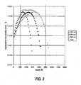
- Figure 2 is a graph illustrating simulation results for a possible impurity profile of silicon ions implanted into a structure including a HPN protective layer on a n- GaN surface layer and a n+ GaN channel layer. As shown in the simulation results of Figure 2 , silicon ions were implanted into the structure in three implant steps under differing sets of implant conditions to provide a substantially uniform dopant concentration.
- the simulation results illustrate silicon ions implanted in the first implant step at a dose of about 0.5x10 15 to about 2.5x10 15 ions/cm 2 and at an implantation energy of about 160 keV, in the second implant step at a dose of about 0.8x10 15 to about 5x10 15 ions/cm 2 and at an implantation energy of about 260keV, and in the third implant step at a dose of about 0.5x10 15 to about 3.7x10 15 ions/cm 2 and at an implantation energy of about 360keV.
- the three-step implant process described above may result in an implanted region having a substantially uniform dopant concentration with a peak concentration of about 5x10 20 ions/cm 3 , which may be desirable for some applications.
- the number of implant steps may depend on the thickness of the protective layer and/or the surface layer, in order to provide the implanted region in contact with the channel layer.
- the combinations of energy, dose, and/or other implant conditions may be optimized for a given structure, and are not limited to those combinations described herein.
- additional layers may be included in a HEMT device while still benefiting from the teachings of the present invention.
- additional layers may include GaN cap layers, as for example, described in Yu et al., "Schottky barrier engineering in III-V nitrides via the piezoelectric effect," Applied Physics Letters, Vol. 73, No. 13, 1998 , or in U.S. Patent Publication No.
- insulating layers such as SiN, or relatively high quality AlN may be deposited for making a MISHEMT and/or passivating the surface.
- the additional layers may also include a compositionally graded transition layer or layers.
- the surface layer 22 may also be provided with multiple layers as described in United States Patent Publication No. 2002/0167023A1, to Smorchkova et al. , entitled "GROUP-III NITRIDE BASED HIGH ELECTRON MOBILITY TRANSISTOR (HEMT) WITH BARRIER/SPACER LAYER" the disclosure of which is incorporated herein by reference as if set forth fully herein.
- embodiments of the present invention should not be construed as limiting the surface/barrier layer to a single layer but may include, for example, insulating layers having combinations of GaN, AlGaN and/or AlN layers.
- a GaN, AlN structure may be utilized to reduce or prevent alloy scattering.
- embodiments of the present invention may include nitride based surface layers, such as AlGaN-based barrier layers, AlN-based barrier layers, and/or combinations thereof.
- embodiments of the present invention may also be employed in connection with other types of devices and/or materials.
- embodiments of the invention may be particularly suited for use in silicon carbide MESFET devices, such as the devices described in U.S. Patent No. 6,686,616 entitled "SILICON CARBIDE METAL-SEMICONDUCTOR FIELD EFFECT TRANSISTORS" the disclosure of which is hereby incorporated herein by reference in their entirety.
- GaN-based light emitting devices LEDs
- GaAs-based devices such as GaAs/AlGaAs pHEMT devices, GaN JFET devices, GaN HJFET devices, heterojunction bipolar transistors (HBTs) including an implanted base contact through the emitter, and/or other opto-electronic or electronic Group III-nitride devices where preservation of as-grown surface properties may be desired.
- LEDs GaN-based light emitting devices
- GaAs-based devices such as GaAs/AlGaAs pHEMT devices, GaN JFET devices, GaN HJFET devices, heterojunction bipolar transistors (HBTs) including an implanted base contact through the emitter, and/or other opto-electronic or electronic Group III-nitride devices where preservation of as-grown surface properties may be desired.
- HBTs heterojunction bipolar transistors
Landscapes
- Engineering & Computer Science (AREA)
- Physics & Mathematics (AREA)
- Microelectronics & Electronic Packaging (AREA)
- General Physics & Mathematics (AREA)
- Manufacturing & Machinery (AREA)
- Computer Hardware Design (AREA)
- Condensed Matter Physics & Semiconductors (AREA)
- Power Engineering (AREA)
- High Energy & Nuclear Physics (AREA)
- Health & Medical Sciences (AREA)
- Toxicology (AREA)
- Junction Field-Effect Transistors (AREA)
- Electrodes Of Semiconductors (AREA)
- Formation Of Insulating Films (AREA)
Applications Claiming Priority (2)
| Application Number | Priority Date | Filing Date | Title |
|---|---|---|---|
| US11/556,871 US8823057B2 (en) | 2006-11-06 | 2006-11-06 | Semiconductor devices including implanted regions for providing low-resistance contact to buried layers and related devices |
| PCT/US2007/023095 WO2008057392A2 (en) | 2006-11-06 | 2007-11-01 | Methods of fabricating semiconductor devices including implanted regions for providing low-resistance contact to buried layers and related devices |
Publications (2)
| Publication Number | Publication Date |
|---|---|
| EP2084733A2 EP2084733A2 (en) | 2009-08-05 |
| EP2084733B1 true EP2084733B1 (en) | 2014-07-30 |
Family
ID=39365054
Family Applications (1)
| Application Number | Title | Priority Date | Filing Date |
|---|---|---|---|
| EP07853067.2A Active EP2084733B1 (en) | 2006-11-06 | 2007-11-01 | Methods of fabricating semiconductor devices including implanted regions for providing low-resistance contact to buried layers and related devices |
Country Status (7)
| Country | Link |
|---|---|
| US (2) | US8823057B2 (enExample) |
| EP (1) | EP2084733B1 (enExample) |
| JP (2) | JP5270562B2 (enExample) |
| KR (1) | KR101344972B1 (enExample) |
| CN (1) | CN101611473B (enExample) |
| CA (1) | CA2666519C (enExample) |
| WO (1) | WO2008057392A2 (enExample) |
Families Citing this family (72)
| Publication number | Priority date | Publication date | Assignee | Title |
|---|---|---|---|---|
| US7501669B2 (en) | 2003-09-09 | 2009-03-10 | Cree, Inc. | Wide bandgap transistor devices with field plates |
| US9773877B2 (en) | 2004-05-13 | 2017-09-26 | Cree, Inc. | Wide bandgap field effect transistors with source connected field plates |
| US11791385B2 (en) | 2005-03-11 | 2023-10-17 | Wolfspeed, Inc. | Wide bandgap transistors with gate-source field plates |
| US9040398B2 (en) * | 2006-05-16 | 2015-05-26 | Cree, Inc. | Method of fabricating seminconductor devices including self aligned refractory contacts |
| JP5183913B2 (ja) * | 2006-11-24 | 2013-04-17 | 住友電工デバイス・イノベーション株式会社 | 半導体装置の製造方法 |
| US7875537B2 (en) * | 2007-08-29 | 2011-01-25 | Cree, Inc. | High temperature ion implantation of nitride based HEMTs |
| JP5369434B2 (ja) * | 2007-12-21 | 2013-12-18 | サンケン電気株式会社 | 双方向スイッチ |
| JP5510325B2 (ja) * | 2008-08-06 | 2014-06-04 | 日本電気株式会社 | 電界効果トランジスタ |
| WO2010016212A1 (ja) * | 2008-08-06 | 2010-02-11 | 日本電気株式会社 | 電界効果トランジスタの製造方法 |
| US8674409B2 (en) * | 2008-12-26 | 2014-03-18 | Renesas Electronics Corporation | Heterojunction field effect transistor, method for producing heterojunction field effect transistor, and electronic device |
| US7915704B2 (en) * | 2009-01-26 | 2011-03-29 | Freescale Semiconductor, Inc. | Schottky diode |
| JP5568891B2 (ja) * | 2009-06-03 | 2014-08-13 | 日本電気株式会社 | ヘテロ接合電界効果トランジスタ、その製造方法 |
| JP2011210751A (ja) * | 2010-03-26 | 2011-10-20 | Nec Corp | Iii族窒化物半導体素子、iii族窒化物半導体素子の製造方法、および電子装置 |
| JP2012033689A (ja) * | 2010-07-30 | 2012-02-16 | Sumitomo Electric Device Innovations Inc | 半導体装置の製造方法 |
| KR20120032258A (ko) * | 2010-09-28 | 2012-04-05 | 삼성엘이디 주식회사 | 질화갈륨계 반도체소자 및 그 제조방법 |
| US8895993B2 (en) | 2011-01-31 | 2014-11-25 | Taiwan Semiconductor Manufacturing Company, Ltd. | Low gate-leakage structure and method for gallium nitride enhancement mode transistor |
| WO2015047421A1 (en) | 2013-09-30 | 2015-04-02 | Hrl Laboratories, Llc | Normally-off iii-nitride transistors with high threshold-voltage and low on-resistance |
| US8697505B2 (en) | 2011-09-15 | 2014-04-15 | Taiwan Semiconductor Manufacturing Company, Ltd. | Method of forming a semiconductor structure |
| JP6054620B2 (ja) * | 2012-03-29 | 2016-12-27 | トランスフォーム・ジャパン株式会社 | 化合物半導体装置及びその製造方法 |
| US9337332B2 (en) * | 2012-04-25 | 2016-05-10 | Hrl Laboratories, Llc | III-Nitride insulating-gate transistors with passivation |
| US9111868B2 (en) * | 2012-06-26 | 2015-08-18 | Freescale Semiconductor, Inc. | Semiconductor device with selectively etched surface passivation |
| US10825924B2 (en) | 2012-06-26 | 2020-11-03 | Nxp Usa, Inc. | Semiconductor device with selectively etched surface passivation |
| US10522670B2 (en) | 2012-06-26 | 2019-12-31 | Nxp Usa, Inc. | Semiconductor device with selectively etched surface passivation |
| EP2747143A1 (en) * | 2012-12-19 | 2014-06-25 | Nxp B.V. | GaN HEMTs and GaN diodes |
| US10164038B2 (en) | 2013-01-30 | 2018-12-25 | Taiwan Semiconductor Manufacturing Company, Ltd. | Method of implanting dopants into a group III-nitride structure and device formed |
| JP5940481B2 (ja) * | 2013-03-22 | 2016-06-29 | 株式会社東芝 | 半導体装置 |
| US9755059B2 (en) | 2013-06-09 | 2017-09-05 | Cree, Inc. | Cascode structures with GaN cap layers |
| US9679981B2 (en) * | 2013-06-09 | 2017-06-13 | Cree, Inc. | Cascode structures for GaN HEMTs |
| US9847411B2 (en) | 2013-06-09 | 2017-12-19 | Cree, Inc. | Recessed field plate transistor structures |
| US9768259B2 (en) * | 2013-07-26 | 2017-09-19 | Cree, Inc. | Controlled ion implantation into silicon carbide using channeling and devices fabricated using controlled ion implantation into silicon carbide using channeling |
| TWI555209B (zh) * | 2013-07-29 | 2016-10-21 | 高效電源轉換公司 | 具有降低的輸出電容之氮化鎵裝置及其製法 |
| TWI602308B (zh) * | 2013-12-17 | 2017-10-11 | 國立清華大學 | 蕭特基二極體元件 |
| WO2015131846A1 (en) * | 2014-03-06 | 2015-09-11 | The Hong Kong University Of Science And Technology | P-doping-free schottky-on-heterojunction light-emitting diode and high-electron-mobility light-emitting transistor |
| US10276712B2 (en) | 2014-05-29 | 2019-04-30 | Hrl Laboratories, Llc | III-nitride field-effect transistor with dual gates |
| US9601574B2 (en) * | 2014-12-29 | 2017-03-21 | Taiwan Semiconductor Manufacturing Company, Ltd. | V-shaped epitaxially formed semiconductor layer |
| US9812532B1 (en) | 2015-08-28 | 2017-11-07 | Hrl Laboratories, Llc | III-nitride P-channel transistor |
| US20170069723A1 (en) * | 2015-09-08 | 2017-03-09 | M/A-Com Technology Solutions Holdings, Inc. | Iii-nitride semiconductor structures comprising multiple spatially patterned implanted species |
| JP6623684B2 (ja) * | 2015-10-29 | 2019-12-25 | 富士通株式会社 | 半導体装置及びその製造方法、電源装置、高周波増幅器 |
| WO2017087197A1 (en) | 2015-11-19 | 2017-05-26 | Hrl Laboratories, Llc | Iii-nitride field-effect transistor with dual gates |
| US10128364B2 (en) | 2016-03-28 | 2018-11-13 | Nxp Usa, Inc. | Semiconductor devices with an enhanced resistivity region and methods of fabrication therefor |
| US10354879B2 (en) * | 2016-06-24 | 2019-07-16 | Cree, Inc. | Depletion mode semiconductor devices including current dependent resistance |
| US9917171B2 (en) * | 2016-07-21 | 2018-03-13 | International Business Machines Corporation | Low-resistive, CMOS-compatible, Au-free ohmic contact to N—InP |
| US10170604B2 (en) * | 2016-08-08 | 2019-01-01 | Atomera Incorporated | Method for making a semiconductor device including a resonant tunneling diode with electron mean free path control layers |
| EP3501033B1 (en) * | 2016-08-18 | 2025-09-24 | Raytheon Company | Semiconductor material growth of a high resistivity nitride buffer layer using ion implantation |
| JP6669029B2 (ja) * | 2016-09-28 | 2020-03-18 | 豊田合成株式会社 | 半導体装置の製造方法 |
| JP6629252B2 (ja) * | 2017-02-01 | 2020-01-15 | 株式会社東芝 | 半導体装置の製造方法 |
| JP6327379B1 (ja) * | 2017-04-03 | 2018-05-23 | 富士電機株式会社 | 窒化ガリウム半導体装置および窒化ガリウム半導体装置の製造方法 |
| JP6834709B2 (ja) * | 2017-04-03 | 2021-02-24 | 住友電気工業株式会社 | 窒化珪素パッシベーション膜の成膜方法及び半導体装置の製造方法 |
| JP6736513B2 (ja) | 2017-04-24 | 2020-08-05 | 株式会社東芝 | 半導体装置、電源回路、及び、コンピュータ |
| JP6920656B2 (ja) * | 2017-06-07 | 2021-08-18 | パナソニックIpマネジメント株式会社 | 半導体電極及びそれを備えたデバイス、並びに、半導体電極の製造方法 |
| WO2019009111A1 (ja) * | 2017-07-07 | 2019-01-10 | パナソニックIpマネジメント株式会社 | 半導体装置およびその製造方法 |
| CN108597997B (zh) * | 2018-02-28 | 2021-03-23 | 中国电子科技集团公司第十三研究所 | GaN基器件欧姆接触电极的制备方法 |
| US11404407B2 (en) * | 2018-06-22 | 2022-08-02 | Intel Corporation | Implants to enlarge Schottky diode cross-sectional area for lateral current conduction |
| CN109216442A (zh) * | 2018-09-11 | 2019-01-15 | 苏州汉骅半导体有限公司 | 半导体结构制造方法 |
| JP7056532B2 (ja) * | 2018-11-29 | 2022-04-19 | 豊田合成株式会社 | p型III族窒化物半導体の製造方法 |
| US11476359B2 (en) * | 2019-03-18 | 2022-10-18 | Wolfspeed, Inc. | Structures for reducing electron concentration and process for reducing electron concentration |
| GB2594308B (en) | 2020-04-23 | 2022-06-08 | X Fab Dresden Gmbh & Co Kg | Semiconductor contact structures |
| CN111613527A (zh) * | 2020-05-20 | 2020-09-01 | 南京大学 | 一种基于Mg离子注入与高温退火工艺实现氮化镓p型掺杂的方法 |
| US11749726B2 (en) | 2020-10-27 | 2023-09-05 | Wolfspeed, Inc. | Field effect transistor with source-connected field plate |
| US11502178B2 (en) | 2020-10-27 | 2022-11-15 | Wolfspeed, Inc. | Field effect transistor with at least partially recessed field plate |
| US12408403B2 (en) | 2020-10-27 | 2025-09-02 | Macom Technology Solutions Holdings, Inc. | Field effect transistor with stacked unit subcell structure |
| US11658234B2 (en) | 2020-10-27 | 2023-05-23 | Wolfspeed, Inc. | Field effect transistor with enhanced reliability |
| US12266721B2 (en) | 2020-10-27 | 2025-04-01 | Wolfspeed, Inc. | Field effect transistor with multiple stepped field plate |
| US11791389B2 (en) | 2021-01-08 | 2023-10-17 | Wolfspeed, Inc. | Radio frequency transistor amplifiers having widened and/or asymmetric source/drain regions for improved on-resistance performance |
| US11869964B2 (en) | 2021-05-20 | 2024-01-09 | Wolfspeed, Inc. | Field effect transistors with modified access regions |
| US12446252B2 (en) * | 2021-05-20 | 2025-10-14 | Macom Technology Solutions Holdings, Inc. | Transistors including semiconductor surface modification and related fabrication methods |
| PL439368A1 (pl) | 2021-10-30 | 2023-05-02 | Instytut Wysokich Ciśnień Polskiej Akademii Nauk Unipress | Sposób wytwarzania obszaru o regularnie zmiennym współczynniku załamania światła w wybranej warstwie warstwowej struktury półprzewodnikowej |
| KR102745209B1 (ko) * | 2022-01-26 | 2024-12-23 | 주식회사 세미콘웍스 | 식각공정 시 에칭 스탑을 검출하기 위한 면저항 측정센서 및 측정시스템 |
| JP7693576B2 (ja) * | 2022-02-09 | 2025-06-17 | 株式会社東芝 | 半導体装置、及び、半導体装置の製造方法 |
| US20240194751A1 (en) * | 2022-12-09 | 2024-06-13 | Wolfspeed, Inc. | Transistor devices including self-aligned ohmic contacts and contact regions and related fabrication methods |
| WO2024204055A1 (ja) * | 2023-03-30 | 2024-10-03 | ヌヴォトンテクノロジージャパン株式会社 | 半導体装置及びその製造方法 |
| CN119767726A (zh) * | 2024-12-31 | 2025-04-04 | 广东省科学院半导体研究所 | 一种氮化镓器件制备方法及氮化镓器件 |
Family Cites Families (196)
| Publication number | Priority date | Publication date | Assignee | Title |
|---|---|---|---|---|
| US3919656A (en) | 1973-04-23 | 1975-11-11 | Nathan O Sokal | High-efficiency tuned switching power amplifier |
| US3955160A (en) | 1975-04-30 | 1976-05-04 | Rca Corporation | Surface acoustic wave device |
| FR2465317A2 (fr) | 1979-03-28 | 1981-03-20 | Thomson Csf | Transistor a effet de champ a frequence de coupure elevee |
| EP0033037B1 (en) | 1979-12-28 | 1990-03-21 | Fujitsu Limited | Heterojunction semiconductor devices |
| US4947232A (en) | 1980-03-22 | 1990-08-07 | Sharp Kabushiki Kaisha | High voltage MOS transistor |
| NL8103218A (nl) | 1981-07-06 | 1983-02-01 | Philips Nv | Veldeffekttransistor met geisoleerde stuurelektrode. |
| JPS58197910A (ja) | 1982-05-14 | 1983-11-17 | Hitachi Ltd | 弾性表面波素子 |
| JPS594084A (ja) * | 1982-06-30 | 1984-01-10 | Fujitsu Ltd | 半導体装置の製造方法 |
| US4551905A (en) | 1982-12-09 | 1985-11-12 | Cornell Research Foundation, Inc. | Fabrication of metal lines for semiconductor devices |
| JPH088350B2 (ja) | 1985-04-08 | 1996-01-29 | 日本電気株式会社 | 半導体装置 |
| US4755867A (en) | 1986-08-15 | 1988-07-05 | American Telephone And Telegraph Company, At&T Bell Laboratories | Vertical Enhancement-mode Group III-V compound MISFETs |
| US4788156A (en) | 1986-09-24 | 1988-11-29 | Microwave Technology, Inc. | Subchannel doping to reduce short-gate effects in field effect transistors |
| JPH0750781B2 (ja) * | 1987-03-18 | 1995-05-31 | 富士通株式会社 | 化合物半導体集積回路装置 |
| US5011549A (en) | 1987-10-26 | 1991-04-30 | North Carolina State University | Homoepitaxial growth of Alpha-SiC thin films and semiconductor devices fabricated thereon |
| US4912064A (en) | 1987-10-26 | 1990-03-27 | North Carolina State University | Homoepitaxial growth of alpha-SiC thin films and semiconductor devices fabricated thereon |
| US4912063A (en) | 1987-10-26 | 1990-03-27 | North Carolina State University | Growth of beta-sic thin films and semiconductor devices fabricated thereon |
| US4866005A (en) | 1987-10-26 | 1989-09-12 | North Carolina State University | Sublimation of silicon carbide to produce large, device quality single crystals of silicon carbide |
| US5411914A (en) | 1988-02-19 | 1995-05-02 | Massachusetts Institute Of Technology | III-V based integrated circuits having low temperature growth buffer or passivation layers |
| EP0334006A1 (en) | 1988-02-22 | 1989-09-27 | Siemens Aktiengesellschaft | Stacked channel heterojunction fet |
| US5196359A (en) | 1988-06-30 | 1993-03-23 | Texas Instruments Incorporated | Method of forming heterostructure field effect transistor |
| EP0353805B1 (en) | 1988-08-05 | 1993-03-03 | Agfa-Gevaert N.V. | Reproduction of x-ray images with photostimulable phosphor |
| US4884001A (en) | 1988-12-13 | 1989-11-28 | United Technologies Corporation | Monolithic electro-acoustic device having an acoustic charge transport device integrated with a transistor |
| US5204278A (en) * | 1989-08-11 | 1993-04-20 | Kabushiki Kaisha Toshiba | Method of making MES field effect transistor using III-V compound semiconductor |
| US4946547A (en) | 1989-10-13 | 1990-08-07 | Cree Research, Inc. | Method of preparing silicon carbide surfaces for crystal growth |
| US5053348A (en) | 1989-12-01 | 1991-10-01 | Hughes Aircraft Company | Fabrication of self-aligned, t-gate hemt |
| US5128279A (en) | 1990-03-05 | 1992-07-07 | Vlsi Technology, Inc. | Charge neutralization using silicon-enriched oxide layer |
| US5057897A (en) | 1990-03-05 | 1991-10-15 | Vlsi Technology, Inc. | Charge neutralization using silicon-enriched oxide layer |
| US5210051A (en) | 1990-03-27 | 1993-05-11 | Cree Research, Inc. | High efficiency light emitting diodes from bipolar gallium nitride |
| US5172197A (en) | 1990-04-11 | 1992-12-15 | Hughes Aircraft Company | Hemt structure with passivated donor layer |
| US5292501A (en) | 1990-06-25 | 1994-03-08 | Degenhardt Charles R | Use of a carboxy-substituted polymer to inhibit plaque formation without tooth staining |
| US5057564A (en) | 1990-07-23 | 1991-10-15 | Exxon Research And Engineering Company | Cyclic carbonyl containing polymers |
| US5236547A (en) * | 1990-09-25 | 1993-08-17 | Kabushiki Kaisha Toshiba | Method of forming a pattern in semiconductor device manufacturing process |
| US5200022A (en) | 1990-10-03 | 1993-04-06 | Cree Research, Inc. | Method of improving mechanically prepared substrate surfaces of alpha silicon carbide for deposition of beta silicon carbide thereon and resulting product |
| US5223458A (en) | 1990-12-18 | 1993-06-29 | Raytheon Company | Method of manufacturing a III-V semiconductor device using a self-biased substrate and a plasma containing an electronegative species |
| US5155062A (en) | 1990-12-20 | 1992-10-13 | Cree Research, Inc. | Method for silicon carbide chemical vapor deposition using levitated wafer system |
| US5192987A (en) | 1991-05-17 | 1993-03-09 | Apa Optics, Inc. | High electron mobility transistor with GaN/Alx Ga1-x N heterojunctions |
| US5270554A (en) | 1991-06-14 | 1993-12-14 | Cree Research, Inc. | High power high frequency metal-semiconductor field-effect transistor formed in silicon carbide |
| JPH0521793A (ja) | 1991-07-09 | 1993-01-29 | Mitsubishi Electric Corp | 半導体装置及びその製造方法 |
| US5254862A (en) * | 1991-08-14 | 1993-10-19 | Kobe Steel U.S.A., Inc. | Diamond field-effect transistor with a particular boron distribution profile |
| US5265267A (en) | 1991-08-29 | 1993-11-23 | Motorola, Inc. | Integrated circuit including a surface acoustic wave transformer and a balanced mixer |
| US5306662A (en) | 1991-11-08 | 1994-04-26 | Nichia Chemical Industries, Ltd. | Method of manufacturing P-type compound semiconductor |
| JP3352712B2 (ja) | 1991-12-18 | 2002-12-03 | 浩 天野 | 窒化ガリウム系半導体素子及びその製造方法 |
| EP0549373B1 (en) | 1991-12-25 | 1995-05-17 | Nec Corporation | Tunnel transistor and method of manufacturing same |
| JPH05183381A (ja) | 1991-12-27 | 1993-07-23 | Nippon Steel Corp | 高周波回路基板および高周波回路素子 |
| JPH05275463A (ja) | 1992-03-30 | 1993-10-22 | Matsushita Electric Ind Co Ltd | 半導体装置 |
| JPH05326561A (ja) | 1992-05-22 | 1993-12-10 | Nec Corp | 電界効果トランジスタの製造方法 |
| US5343054A (en) * | 1992-09-14 | 1994-08-30 | Kabushiki Kaisha Toshiba | Semiconductor light-detection device with recombination rates |
| JPH06224225A (ja) | 1993-01-27 | 1994-08-12 | Fujitsu Ltd | 電界効果半導体装置 |
| JPH06267991A (ja) | 1993-03-12 | 1994-09-22 | Hitachi Ltd | 半導体装置およびその製造方法 |
| US5393993A (en) | 1993-12-13 | 1995-02-28 | Cree Research, Inc. | Buffer structure between silicon carbide and gallium nitride and resulting semiconductor devices |
| US5686737A (en) | 1994-09-16 | 1997-11-11 | Cree Research, Inc. | Self-aligned field-effect transistor for high frequency applications |
| US5592501A (en) | 1994-09-20 | 1997-01-07 | Cree Research, Inc. | Low-strain laser structures with group III nitride active layers |
| US5523589A (en) | 1994-09-20 | 1996-06-04 | Cree Research, Inc. | Vertical geometry light emitting diode with group III nitride active layer and extended lifetime |
| US5576589A (en) | 1994-10-13 | 1996-11-19 | Kobe Steel Usa, Inc. | Diamond surface acoustic wave devices |
| US5670798A (en) | 1995-03-29 | 1997-09-23 | North Carolina State University | Integrated heterostructures of Group III-V nitride semiconductor materials including epitaxial ohmic contact non-nitride buffer layer and methods of fabricating same |
| US5739554A (en) | 1995-05-08 | 1998-04-14 | Cree Research, Inc. | Double heterojunction light emitting diode with gallium nitride active layer |
| US6002148A (en) | 1995-06-30 | 1999-12-14 | Motorola, Inc. | Silicon carbide transistor and method |
| US5569937A (en) | 1995-08-28 | 1996-10-29 | Motorola | High breakdown voltage silicon carbide transistor |
| US5569943A (en) | 1995-09-01 | 1996-10-29 | The United States Of America As Represented By The Secretary Of The Army | Field effect real space transistor |
| JPH09139494A (ja) | 1995-11-16 | 1997-05-27 | Mitsubishi Electric Corp | 半導体装置の製造方法,及び半導体装置 |
| KR100195269B1 (ko) | 1995-12-22 | 1999-06-15 | 윤종용 | 액정표시장치의 제조방법 |
| US5915164A (en) | 1995-12-28 | 1999-06-22 | U.S. Philips Corporation | Methods of making high voltage GaN-A1N based semiconductor devices |
| DE19600116C2 (de) | 1996-01-03 | 2001-03-15 | Siemens Ag | Doppelheterostruktur-HEMT |
| JPH09232827A (ja) | 1996-02-21 | 1997-09-05 | Oki Electric Ind Co Ltd | 半導体装置及び送受信切り替え型アンテナスイッチ回路 |
| JPH1050982A (ja) | 1996-07-31 | 1998-02-20 | Nippon Telegr & Teleph Corp <Ntt> | 半導体装置 |
| US6936839B2 (en) | 1996-10-16 | 2005-08-30 | The University Of Connecticut | Monolithic integrated circuit including a waveguide and quantum well inversion channel devices and a method of fabricating same |
| US5929467A (en) | 1996-12-04 | 1999-07-27 | Sony Corporation | Field effect transistor with nitride compound |
| JP3767759B2 (ja) * | 1997-02-07 | 2006-04-19 | 株式会社村田製作所 | 電界効果型半導体素子 |
| JP3156620B2 (ja) | 1997-02-12 | 2001-04-16 | 日本電気株式会社 | 電界効果トランジスタ及びその製造方法 |
| US6217662B1 (en) | 1997-03-24 | 2001-04-17 | Cree, Inc. | Susceptor designs for silicon carbide thin films |
| US6448648B1 (en) | 1997-03-27 | 2002-09-10 | The United States Of America As Represented By The Secretary Of The Navy | Metalization of electronic semiconductor devices |
| JPH10335595A (ja) * | 1997-03-31 | 1998-12-18 | Sharp Corp | 増幅器用半導体素子、増幅器用半導体素子の製造方法および増幅器用半導体装置 |
| JPH10335637A (ja) | 1997-05-30 | 1998-12-18 | Sony Corp | ヘテロ接合電界効果トランジスタ |
| JP3958404B2 (ja) | 1997-06-06 | 2007-08-15 | 三菱電機株式会社 | 横型高耐圧素子を有する半導体装置 |
| JP3120756B2 (ja) | 1997-06-16 | 2000-12-25 | 日本電気株式会社 | 電界効果トランジスタ及びその製造方法 |
| US6316820B1 (en) | 1997-07-25 | 2001-11-13 | Hughes Electronics Corporation | Passivation layer and process for semiconductor devices |
| JPH1154527A (ja) | 1997-07-30 | 1999-02-26 | Fujitsu Ltd | 電界効果トランジスタおよびその製造方法 |
| JP3457511B2 (ja) | 1997-07-30 | 2003-10-20 | 株式会社東芝 | 半導体装置及びその製造方法 |
| US5943565A (en) * | 1997-09-05 | 1999-08-24 | Advanced Micro Devices, Inc. | CMOS processing employing separate spacers for independently optimized transistor performance |
| US6242327B1 (en) | 1997-09-19 | 2001-06-05 | Fujitsu Limited | Compound semiconductor device having a reduced source resistance |
| JP3653652B2 (ja) * | 1997-09-25 | 2005-06-02 | 富士通株式会社 | 半導体装置 |
| US6201262B1 (en) | 1997-10-07 | 2001-03-13 | Cree, Inc. | Group III nitride photonic devices on silicon carbide substrates with conductive buffer interlay structure |
| US6063186A (en) | 1997-12-17 | 2000-05-16 | Cree, Inc. | Growth of very uniform silicon carbide epitaxial layers |
| US6346451B1 (en) | 1997-12-24 | 2002-02-12 | Philips Electronics North America Corporation | Laterial thin-film silicon-on-insulator (SOI) device having a gate electrode and a field plate electrode |
| DE19800647C1 (de) | 1998-01-09 | 1999-05-27 | Siemens Ag | SOI-Hochspannungsschalter |
| JP3372470B2 (ja) | 1998-01-20 | 2003-02-04 | シャープ株式会社 | 窒化物系iii−v族化合物半導体装置 |
| US6150680A (en) | 1998-03-05 | 2000-11-21 | Welch Allyn, Inc. | Field effect semiconductor device having dipole barrier |
| JPH11261053A (ja) | 1998-03-09 | 1999-09-24 | Furukawa Electric Co Ltd:The | 高移動度トランジスタ |
| US6086673A (en) | 1998-04-02 | 2000-07-11 | Massachusetts Institute Of Technology | Process for producing high-quality III-V nitride substrates |
| US6020226A (en) * | 1998-04-14 | 2000-02-01 | The United States Of America As Represented By The Secretary Of The Air Force | Single layer integrated metal process for enhancement mode field-effect transistor |
| US6316793B1 (en) * | 1998-06-12 | 2001-11-13 | Cree, Inc. | Nitride based transistors on semi-insulating silicon carbide substrates |
| JP3111985B2 (ja) | 1998-06-16 | 2000-11-27 | 日本電気株式会社 | 電界効果型トランジスタ |
| US6246076B1 (en) | 1998-08-28 | 2001-06-12 | Cree, Inc. | Layered dielectric on silicon carbide semiconductor structures |
| JP3180776B2 (ja) | 1998-09-22 | 2001-06-25 | 日本電気株式会社 | 電界効果型トランジスタ |
| KR100316383B1 (ko) | 1998-10-30 | 2002-02-19 | 윤덕용 | 모노리딕직접회로위에박막또는후막단결정압전소자를집적한단일칩라디오구조및그제조방법 |
| US6297092B1 (en) | 1998-12-02 | 2001-10-02 | Micron Technology, Inc. | Method and structure for an oxide layer overlaying an oxidation-resistant layer |
| US6495409B1 (en) | 1999-01-26 | 2002-12-17 | Agere Systems Inc. | MOS transistor having aluminum nitride gate structure and method of manufacturing same |
| JP3209270B2 (ja) | 1999-01-29 | 2001-09-17 | 日本電気株式会社 | ヘテロ接合電界効果トランジスタ |
| US6518637B1 (en) | 1999-04-08 | 2003-02-11 | Wayne State University | Cubic (zinc-blende) aluminum nitride |
| US6218680B1 (en) | 1999-05-18 | 2001-04-17 | Cree, Inc. | Semi-insulating silicon carbide without vanadium domination |
| US6396080B2 (en) | 1999-05-18 | 2002-05-28 | Cree, Inc | Semi-insulating silicon carbide without vanadium domination |
| US6265727B1 (en) | 1999-06-09 | 2001-07-24 | Cree Lighting Company | Solar blind photodiode having an active region with a larger bandgap than one or both if its surrounding doped regions |
| JP2001007379A (ja) | 1999-06-24 | 2001-01-12 | Sharp Corp | 窒化ガリウム系化合物半導体受光素子 |
| US6300706B1 (en) | 1999-07-14 | 2001-10-09 | The United States Of America As Represented By The Secretary Of The Army | Compound semiconductor monolithic frequency sources and actuators |
| JP2001085670A (ja) | 1999-09-14 | 2001-03-30 | Nec Corp | 電界効果型トランジスタ及びその製造方法 |
| US6639255B2 (en) | 1999-12-08 | 2003-10-28 | Matsushita Electric Industrial Co., Ltd. | GaN-based HFET having a surface-leakage reducing cap layer |
| JP4592938B2 (ja) | 1999-12-08 | 2010-12-08 | パナソニック株式会社 | 半導体装置 |
| JP3393602B2 (ja) | 2000-01-13 | 2003-04-07 | 松下電器産業株式会社 | 半導体装置 |
| US6586781B2 (en) | 2000-02-04 | 2003-07-01 | Cree Lighting Company | Group III nitride based FETs and HEMTs with reduced trapping and method for producing the same |
| JP4667556B2 (ja) | 2000-02-18 | 2011-04-13 | 古河電気工業株式会社 | 縦型GaN系電界効果トランジスタ、バイポーラトランジスタと縦型GaN系電界効果トランジスタの製造方法 |
| US6498111B1 (en) | 2000-08-23 | 2002-12-24 | Cree Lighting Company | Fabrication of semiconductor materials and devices with controlled electrical conductivity |
| US6475889B1 (en) | 2000-04-11 | 2002-11-05 | Cree, Inc. | Method of forming vias in silicon carbide and resulting devices and circuits |
| GB2366104B (en) | 2000-05-01 | 2002-10-23 | Murata Manufacturing Co | Surface acoustic wave device, shear bulk wave transducer, and longitudinal bulk wave transducer |
| US6686616B1 (en) | 2000-05-10 | 2004-02-03 | Cree, Inc. | Silicon carbide metal-semiconductor field effect transistors |
| JP4022708B2 (ja) | 2000-06-29 | 2007-12-19 | 日本電気株式会社 | 半導体装置 |
| JP4186032B2 (ja) | 2000-06-29 | 2008-11-26 | 日本電気株式会社 | 半導体装置 |
| US6515316B1 (en) | 2000-07-14 | 2003-02-04 | Trw Inc. | Partially relaxed channel HEMT device |
| TWI257179B (en) | 2000-07-17 | 2006-06-21 | Fujitsu Quantum Devices Ltd | High-speed compound semiconductor device operable at large output power with minimum leakage current |
| US6555946B1 (en) | 2000-07-24 | 2003-04-29 | Motorola, Inc. | Acoustic wave device and process for forming the same |
| US6690042B2 (en) | 2000-09-27 | 2004-02-10 | Sensor Electronic Technology, Inc. | Metal oxide semiconductor heterostructure field effect transistor |
| US6548333B2 (en) | 2000-12-01 | 2003-04-15 | Cree, Inc. | Aluminum gallium nitride/gallium nitride high electron mobility transistors having a gate contact on a gallium nitride based cap segment |
| JP3428962B2 (ja) | 2000-12-19 | 2003-07-22 | 古河電気工業株式会社 | GaN系高移動度トランジスタ |
| TW466768B (en) | 2000-12-30 | 2001-12-01 | Nat Science Council | An In0.34Al0.66As0.85Sb0.15/InP HFET utilizing InP channels |
| US6569250B2 (en) | 2001-01-08 | 2003-05-27 | Cree, Inc. | Gas-driven rotation apparatus and method for forming silicon carbide layers |
| US6828879B2 (en) | 2001-02-16 | 2004-12-07 | Sanyo Electric Co., Ltd. | Longitudinal coupled multiple mode surface acoustic wave filter |
| US6468878B1 (en) | 2001-02-27 | 2002-10-22 | Koninklijke Philips Electronics N.V. | SOI LDMOS structure with improved switching characteristics |
| GB0107408D0 (en) | 2001-03-23 | 2001-05-16 | Koninkl Philips Electronics Nv | Field effect transistor structure and method of manufacture |
| JP3648462B2 (ja) | 2001-04-27 | 2005-05-18 | 沖電気工業株式会社 | 弾性表面波分波器 |
| US6849882B2 (en) | 2001-05-11 | 2005-02-01 | Cree Inc. | Group-III nitride based high electron mobility transistor (HEMT) with barrier/spacer layer |
| US6706114B2 (en) | 2001-05-21 | 2004-03-16 | Cree, Inc. | Methods of fabricating silicon carbide crystals |
| US6525378B1 (en) * | 2001-06-13 | 2003-02-25 | Advanced Micro Devices, Inc. | Raised S/D region for optimal silicidation to control floating body effects in SOI devices |
| US6475857B1 (en) | 2001-06-21 | 2002-11-05 | Samsung Electronics Co., Ltd. | Method of making a scalable two transistor memory device |
| US20030015708A1 (en) * | 2001-07-23 | 2003-01-23 | Primit Parikh | Gallium nitride based diodes with low forward voltage and low reverse current operation |
| EP2267783B1 (en) | 2001-07-24 | 2017-06-21 | Cree, Inc. | Insulating gate algan/gan hemt |
| US20030022412A1 (en) | 2001-07-25 | 2003-01-30 | Motorola, Inc. | Monolithic semiconductor-piezoelectric device structures and electroacoustic charge transport devices |
| US20030030119A1 (en) | 2001-08-13 | 2003-02-13 | Motorola, Inc. | Structure and method for improved piezo electric coupled component integrated devices |
| US6896738B2 (en) | 2001-10-30 | 2005-05-24 | Cree, Inc. | Induction heating devices and methods for controllably heating an article |
| WO2003038905A2 (en) | 2001-11-01 | 2003-05-08 | Koninklijke Philips Electronics N.V. | Lateral soi field-effect transistor |
| US7030428B2 (en) | 2001-12-03 | 2006-04-18 | Cree, Inc. | Strain balanced nitride heterojunction transistors |
| KR100445904B1 (ko) | 2001-12-12 | 2004-08-25 | 한국전자통신연구원 | 소스 필드 플레이트를 갖는 드레인 확장형 모스 전계 효과트랜지스터 및그 제조방법 |
| JP4157707B2 (ja) | 2002-01-16 | 2008-10-01 | 株式会社東芝 | 磁気メモリ |
| US7138291B2 (en) | 2003-01-30 | 2006-11-21 | Cree, Inc. | Methods of treating a silicon carbide substrate for improved epitaxial deposition and resulting structures and devices |
| DE10206739C1 (de) | 2002-02-18 | 2003-08-21 | Infineon Technologies Ag | Transistorbauelement |
| JP3908572B2 (ja) | 2002-03-18 | 2007-04-25 | 株式会社東芝 | 半導体素子 |
| JP3705431B2 (ja) | 2002-03-28 | 2005-10-12 | ユーディナデバイス株式会社 | 半導体装置及びその製造方法 |
| US6797069B2 (en) | 2002-04-08 | 2004-09-28 | Cree, Inc. | Gas driven planetary rotation apparatus and methods for forming silicon carbide layers |
| US6559513B1 (en) | 2002-04-22 | 2003-05-06 | M/A-Com, Inc. | Field-plate MESFET |
| US6852615B2 (en) | 2002-06-10 | 2005-02-08 | Hrl Laboratories, Llc | Ohmic contacts for high electron mobility transistors and a method of making the same |
| US6982204B2 (en) | 2002-07-16 | 2006-01-03 | Cree, Inc. | Nitride-based transistors and methods of fabrication thereof using non-etched contact recesses |
| JP3790500B2 (ja) * | 2002-07-16 | 2006-06-28 | ユーディナデバイス株式会社 | 電界効果トランジスタ及びその製造方法 |
| US6735492B2 (en) | 2002-07-19 | 2004-05-11 | International Business Machines Corporation | Feedback method utilizing lithographic exposure field dimensions to predict process tool overlay settings |
| US20050189651A1 (en) * | 2002-07-25 | 2005-09-01 | Matsushita Elec. Ind. Co. Ltd. | Contact formation method and semiconductor device |
| JP2004111910A (ja) * | 2002-07-25 | 2004-04-08 | Matsushita Electric Ind Co Ltd | コンタクト形成方法および半導体装置 |
| US6884704B2 (en) | 2002-08-05 | 2005-04-26 | Hrl Laboratories, Llc | Ohmic metal contact and channel protection in GaN devices using an encapsulation layer |
| US20040021152A1 (en) | 2002-08-05 | 2004-02-05 | Chanh Nguyen | Ga/A1GaN Heterostructure Field Effect Transistor with dielectric recessed gate |
| JP2004093683A (ja) * | 2002-08-29 | 2004-03-25 | Casio Comput Co Ltd | コンテンツ配信システム、及びプログラム |
| US6903385B2 (en) | 2002-10-09 | 2005-06-07 | Sensor Electronic Technology, Inc. | Semiconductor structure having a textured nitride-based layer |
| JP4050128B2 (ja) * | 2002-10-24 | 2008-02-20 | 松下電器産業株式会社 | ヘテロ接合電界効果型トランジスタ及びその製造方法 |
| JP4385206B2 (ja) | 2003-01-07 | 2009-12-16 | 日本電気株式会社 | 電界効果トランジスタ |
| CN100388509C (zh) | 2003-01-29 | 2008-05-14 | 株式会社东芝 | 功率半导体器件 |
| US6716690B1 (en) * | 2003-03-12 | 2004-04-06 | Advanced Micro Devices, Inc. | Uniformly doped source/drain junction in a double-gate MOSFET |
| JP4746825B2 (ja) | 2003-05-15 | 2011-08-10 | 富士通株式会社 | 化合物半導体装置 |
| JP4417677B2 (ja) | 2003-09-19 | 2010-02-17 | 株式会社東芝 | 電力用半導体装置 |
| US20050133816A1 (en) | 2003-12-19 | 2005-06-23 | Zhaoyang Fan | III-nitride quantum-well field effect transistors |
| US7135715B2 (en) | 2004-01-07 | 2006-11-14 | Cree, Inc. | Co-doping for fermi level control in semi-insulating Group III nitrides |
| US7045404B2 (en) * | 2004-01-16 | 2006-05-16 | Cree, Inc. | Nitride-based transistors with a protective layer and a low-damage recess and methods of fabrication thereof |
| US7033912B2 (en) | 2004-01-22 | 2006-04-25 | Cree, Inc. | Silicon carbide on diamond substrates and related devices and methods |
| US7170111B2 (en) | 2004-02-05 | 2007-01-30 | Cree, Inc. | Nitride heterojunction transistors having charge-transfer induced energy barriers and methods of fabricating the same |
| JP4539105B2 (ja) | 2004-02-12 | 2010-09-08 | 日立電線株式会社 | 窒化物半導体デバイスの製造方法 |
| JP2005276978A (ja) * | 2004-03-24 | 2005-10-06 | Nissan Motor Co Ltd | オーミック電極構造体の製造方法、オーミック電極構造体、半導体装置の製造方法および半導体装置 |
| JP2005286135A (ja) * | 2004-03-30 | 2005-10-13 | Eudyna Devices Inc | 半導体装置および半導体装置の製造方法 |
| JP4869563B2 (ja) | 2004-04-21 | 2012-02-08 | 新日本無線株式会社 | 窒化物半導体装置及びその製造方法 |
| JP4398780B2 (ja) * | 2004-04-30 | 2010-01-13 | 古河電気工業株式会社 | GaN系半導体装置 |
| US7432142B2 (en) | 2004-05-20 | 2008-10-07 | Cree, Inc. | Methods of fabricating nitride-based transistors having regrown ohmic contact regions |
| US7084441B2 (en) | 2004-05-20 | 2006-08-01 | Cree, Inc. | Semiconductor devices having a hybrid channel layer, current aperture transistors and methods of fabricating same |
| US7332795B2 (en) | 2004-05-22 | 2008-02-19 | Cree, Inc. | Dielectric passivation for semiconductor devices |
| JP2006032911A (ja) * | 2004-06-15 | 2006-02-02 | Ngk Insulators Ltd | 半導体積層構造、半導体素子およびhemt素子 |
| JP5248743B2 (ja) * | 2004-06-30 | 2013-07-31 | アイメック | 半導体装置および半導体装置の製造方法 |
| JP2006032552A (ja) | 2004-07-14 | 2006-02-02 | Toshiba Corp | 窒化物含有半導体装置 |
| US7238560B2 (en) | 2004-07-23 | 2007-07-03 | Cree, Inc. | Methods of fabricating nitride-based transistors with a cap layer and a recessed gate |
| US20060017064A1 (en) | 2004-07-26 | 2006-01-26 | Saxler Adam W | Nitride-based transistors having laterally grown active region and methods of fabricating same |
| US7312481B2 (en) | 2004-10-01 | 2007-12-25 | Texas Instruments Incorporated | Reliable high-voltage junction field effect transistor and method of manufacture therefor |
| JP2006134935A (ja) * | 2004-11-02 | 2006-05-25 | Mitsubishi Electric Corp | 半導体装置およびその製造方法 |
| US7456443B2 (en) | 2004-11-23 | 2008-11-25 | Cree, Inc. | Transistors having buried n-type and p-type regions beneath the source region |
| US7161194B2 (en) | 2004-12-06 | 2007-01-09 | Cree, Inc. | High power density and/or linearity transistors |
| US7355215B2 (en) | 2004-12-06 | 2008-04-08 | Cree, Inc. | Field effect transistors (FETs) having multi-watt output power at millimeter-wave frequencies |
| US7236053B2 (en) | 2004-12-31 | 2007-06-26 | Cree, Inc. | High efficiency switch-mode power amplifier |
| JP4940557B2 (ja) * | 2005-02-08 | 2012-05-30 | 日本電気株式会社 | 電界効果トランジスタ及びその製造方法 |
| US11791385B2 (en) | 2005-03-11 | 2023-10-17 | Wolfspeed, Inc. | Wide bandgap transistors with gate-source field plates |
| US7465967B2 (en) | 2005-03-15 | 2008-12-16 | Cree, Inc. | Group III nitride field effect transistors (FETS) capable of withstanding high temperature reverse bias test conditions |
| US20060226442A1 (en) * | 2005-04-07 | 2006-10-12 | An-Ping Zhang | GaN-based high electron mobility transistor and method for making the same |
| US8575651B2 (en) | 2005-04-11 | 2013-11-05 | Cree, Inc. | Devices having thick semi-insulating epitaxial gallium nitride layer |
| US7626217B2 (en) | 2005-04-11 | 2009-12-01 | Cree, Inc. | Composite substrates of conductive and insulating or semi-insulating group III-nitrides for group III-nitride devices |
| US7615774B2 (en) | 2005-04-29 | 2009-11-10 | Cree.Inc. | Aluminum free group III-nitride based high electron mobility transistors |
| US7544963B2 (en) | 2005-04-29 | 2009-06-09 | Cree, Inc. | Binary group III-nitride based high electron mobility transistors |
| US20090250785A1 (en) * | 2008-04-02 | 2009-10-08 | Thomas Joseph Krutsick | Methods of forming a shallow base region of a bipolar transistor |
-
2006
- 2006-11-06 US US11/556,871 patent/US8823057B2/en active Active
-
2007
- 2007-11-01 JP JP2009536251A patent/JP5270562B2/ja active Active
- 2007-11-01 KR KR1020097011435A patent/KR101344972B1/ko active Active
- 2007-11-01 CN CN2007800494033A patent/CN101611473B/zh active Active
- 2007-11-01 WO PCT/US2007/023095 patent/WO2008057392A2/en not_active Ceased
- 2007-11-01 CA CA2666519A patent/CA2666519C/en active Active
- 2007-11-01 EP EP07853067.2A patent/EP2084733B1/en active Active
-
2013
- 2013-05-09 JP JP2013099518A patent/JP5926216B2/ja active Active
-
2014
- 2014-07-16 US US14/332,575 patent/US9984881B2/en active Active
Also Published As
| Publication number | Publication date |
|---|---|
| WO2008057392A3 (en) | 2008-12-24 |
| KR101344972B1 (ko) | 2013-12-24 |
| JP5926216B2 (ja) | 2016-05-25 |
| JP2010509770A (ja) | 2010-03-25 |
| CN101611473A (zh) | 2009-12-23 |
| WO2008057392A2 (en) | 2008-05-15 |
| US8823057B2 (en) | 2014-09-02 |
| JP5270562B2 (ja) | 2013-08-21 |
| CA2666519C (en) | 2016-06-07 |
| EP2084733A2 (en) | 2009-08-05 |
| CN101611473B (zh) | 2012-09-05 |
| US20140329367A1 (en) | 2014-11-06 |
| US9984881B2 (en) | 2018-05-29 |
| JP2013179337A (ja) | 2013-09-09 |
| CA2666519A1 (en) | 2008-05-15 |
| KR20090090325A (ko) | 2009-08-25 |
| US20080121895A1 (en) | 2008-05-29 |
Similar Documents
| Publication | Publication Date | Title |
|---|---|---|
| EP2084733B1 (en) | Methods of fabricating semiconductor devices including implanted regions for providing low-resistance contact to buried layers and related devices | |
| EP1798762B1 (en) | Method of forming semiconductor devices including implanted regions and protective layers | |
| EP2018663B1 (en) | Method of fabricating semiconductor devices including self aligned refractory contacts | |
| US9711633B2 (en) | Methods of forming group III-nitride semiconductor devices including implanting ions directly into source and drain regions and annealing to activate the implanted ions | |
| EP1974373B1 (en) | Methods of fabricating transistors including supported gate electrodes and related devices | |
| US8481376B2 (en) | Group III nitride semiconductor devices with silicon nitride layers and methods of manufacturing such devices | |
| EP2117039B1 (en) | Semiconductor devices including shallow inplanted regions and methods of forming the same |
Legal Events
| Date | Code | Title | Description |
|---|---|---|---|
| PUAI | Public reference made under article 153(3) epc to a published international application that has entered the european phase |
Free format text: ORIGINAL CODE: 0009012 |
|
| 17P | Request for examination filed |
Effective date: 20090429 |
|
| AK | Designated contracting states |
Kind code of ref document: A2 Designated state(s): AT BE BG CH CY CZ DE DK EE ES FI FR GB GR HU IE IS IT LI LT LU LV MC MT NL PL PT RO SE SI SK TR |
|
| DAX | Request for extension of the european patent (deleted) | ||
| 17Q | First examination report despatched |
Effective date: 20120927 |
|
| GRAP | Despatch of communication of intention to grant a patent |
Free format text: ORIGINAL CODE: EPIDOSNIGR1 |
|
| INTG | Intention to grant announced |
Effective date: 20140210 |
|
| GRAS | Grant fee paid |
Free format text: ORIGINAL CODE: EPIDOSNIGR3 |
|
| GRAA | (expected) grant |
Free format text: ORIGINAL CODE: 0009210 |
|
| AK | Designated contracting states |
Kind code of ref document: B1 Designated state(s): AT BE BG CH CY CZ DE DK EE ES FI FR GB GR HU IE IS IT LI LT LU LV MC MT NL PL PT RO SE SI SK TR |
|
| REG | Reference to a national code |
Ref country code: GB Ref legal event code: FG4D |
|
| REG | Reference to a national code |
Ref country code: CH Ref legal event code: EP |
|
| REG | Reference to a national code |
Ref country code: AT Ref legal event code: REF Ref document number: 680317 Country of ref document: AT Kind code of ref document: T Effective date: 20140815 |
|
| REG | Reference to a national code |
Ref country code: IE Ref legal event code: FG4D |
|
| REG | Reference to a national code |
Ref country code: DE Ref legal event code: R096 Ref document number: 602007037925 Country of ref document: DE Effective date: 20140911 |
|
| REG | Reference to a national code |
Ref country code: NL Ref legal event code: T3 |
|
| REG | Reference to a national code |
Ref country code: LT Ref legal event code: MG4D |
|
| PG25 | Lapsed in a contracting state [announced via postgrant information from national office to epo] |
Ref country code: FI Free format text: LAPSE BECAUSE OF FAILURE TO SUBMIT A TRANSLATION OF THE DESCRIPTION OR TO PAY THE FEE WITHIN THE PRESCRIBED TIME-LIMIT Effective date: 20140730 Ref country code: LT Free format text: LAPSE BECAUSE OF FAILURE TO SUBMIT A TRANSLATION OF THE DESCRIPTION OR TO PAY THE FEE WITHIN THE PRESCRIBED TIME-LIMIT Effective date: 20140730 Ref country code: BG Free format text: LAPSE BECAUSE OF FAILURE TO SUBMIT A TRANSLATION OF THE DESCRIPTION OR TO PAY THE FEE WITHIN THE PRESCRIBED TIME-LIMIT Effective date: 20141030 Ref country code: PT Free format text: LAPSE BECAUSE OF FAILURE TO SUBMIT A TRANSLATION OF THE DESCRIPTION OR TO PAY THE FEE WITHIN THE PRESCRIBED TIME-LIMIT Effective date: 20141202 Ref country code: ES Free format text: LAPSE BECAUSE OF FAILURE TO SUBMIT A TRANSLATION OF THE DESCRIPTION OR TO PAY THE FEE WITHIN THE PRESCRIBED TIME-LIMIT Effective date: 20140730 Ref country code: GR Free format text: LAPSE BECAUSE OF FAILURE TO SUBMIT A TRANSLATION OF THE DESCRIPTION OR TO PAY THE FEE WITHIN THE PRESCRIBED TIME-LIMIT Effective date: 20141031 Ref country code: SE Free format text: LAPSE BECAUSE OF FAILURE TO SUBMIT A TRANSLATION OF THE DESCRIPTION OR TO PAY THE FEE WITHIN THE PRESCRIBED TIME-LIMIT Effective date: 20140730 |
|
| PG25 | Lapsed in a contracting state [announced via postgrant information from national office to epo] |
Ref country code: PL Free format text: LAPSE BECAUSE OF FAILURE TO SUBMIT A TRANSLATION OF THE DESCRIPTION OR TO PAY THE FEE WITHIN THE PRESCRIBED TIME-LIMIT Effective date: 20140730 Ref country code: LV Free format text: LAPSE BECAUSE OF FAILURE TO SUBMIT A TRANSLATION OF THE DESCRIPTION OR TO PAY THE FEE WITHIN THE PRESCRIBED TIME-LIMIT Effective date: 20140730 Ref country code: CY Free format text: LAPSE BECAUSE OF FAILURE TO SUBMIT A TRANSLATION OF THE DESCRIPTION OR TO PAY THE FEE WITHIN THE PRESCRIBED TIME-LIMIT Effective date: 20140730 Ref country code: IS Free format text: LAPSE BECAUSE OF FAILURE TO SUBMIT A TRANSLATION OF THE DESCRIPTION OR TO PAY THE FEE WITHIN THE PRESCRIBED TIME-LIMIT Effective date: 20141130 |
|
| PG25 | Lapsed in a contracting state [announced via postgrant information from national office to epo] |
Ref country code: RO Free format text: LAPSE BECAUSE OF FAILURE TO SUBMIT A TRANSLATION OF THE DESCRIPTION OR TO PAY THE FEE WITHIN THE PRESCRIBED TIME-LIMIT Effective date: 20140730 Ref country code: IT Free format text: LAPSE BECAUSE OF FAILURE TO SUBMIT A TRANSLATION OF THE DESCRIPTION OR TO PAY THE FEE WITHIN THE PRESCRIBED TIME-LIMIT Effective date: 20140730 Ref country code: CZ Free format text: LAPSE BECAUSE OF FAILURE TO SUBMIT A TRANSLATION OF THE DESCRIPTION OR TO PAY THE FEE WITHIN THE PRESCRIBED TIME-LIMIT Effective date: 20140730 Ref country code: SK Free format text: LAPSE BECAUSE OF FAILURE TO SUBMIT A TRANSLATION OF THE DESCRIPTION OR TO PAY THE FEE WITHIN THE PRESCRIBED TIME-LIMIT Effective date: 20140730 Ref country code: DK Free format text: LAPSE BECAUSE OF FAILURE TO SUBMIT A TRANSLATION OF THE DESCRIPTION OR TO PAY THE FEE WITHIN THE PRESCRIBED TIME-LIMIT Effective date: 20140730 Ref country code: EE Free format text: LAPSE BECAUSE OF FAILURE TO SUBMIT A TRANSLATION OF THE DESCRIPTION OR TO PAY THE FEE WITHIN THE PRESCRIBED TIME-LIMIT Effective date: 20140730 |
|
| REG | Reference to a national code |
Ref country code: DE Ref legal event code: R097 Ref document number: 602007037925 Country of ref document: DE |
|
| PLBE | No opposition filed within time limit |
Free format text: ORIGINAL CODE: 0009261 |
|
| STAA | Information on the status of an ep patent application or granted ep patent |
Free format text: STATUS: NO OPPOSITION FILED WITHIN TIME LIMIT |
|
| PG25 | Lapsed in a contracting state [announced via postgrant information from national office to epo] |
Ref country code: MC Free format text: LAPSE BECAUSE OF FAILURE TO SUBMIT A TRANSLATION OF THE DESCRIPTION OR TO PAY THE FEE WITHIN THE PRESCRIBED TIME-LIMIT Effective date: 20140730 Ref country code: BE Free format text: LAPSE BECAUSE OF NON-PAYMENT OF DUE FEES Effective date: 20141130 Ref country code: LU Free format text: LAPSE BECAUSE OF FAILURE TO SUBMIT A TRANSLATION OF THE DESCRIPTION OR TO PAY THE FEE WITHIN THE PRESCRIBED TIME-LIMIT Effective date: 20141101 |
|
| REG | Reference to a national code |
Ref country code: CH Ref legal event code: PL |
|
| 26N | No opposition filed |
Effective date: 20150504 |
|
| PG25 | Lapsed in a contracting state [announced via postgrant information from national office to epo] |
Ref country code: LI Free format text: LAPSE BECAUSE OF NON-PAYMENT OF DUE FEES Effective date: 20141130 Ref country code: CH Free format text: LAPSE BECAUSE OF NON-PAYMENT OF DUE FEES Effective date: 20141130 |
|
| REG | Reference to a national code |
Ref country code: IE Ref legal event code: MM4A |
|
| REG | Reference to a national code |
Ref country code: FR Ref legal event code: PLFP Year of fee payment: 9 |
|
| PG25 | Lapsed in a contracting state [announced via postgrant information from national office to epo] |
Ref country code: IE Free format text: LAPSE BECAUSE OF NON-PAYMENT OF DUE FEES Effective date: 20141101 |
|
| PG25 | Lapsed in a contracting state [announced via postgrant information from national office to epo] |
Ref country code: SI Free format text: LAPSE BECAUSE OF FAILURE TO SUBMIT A TRANSLATION OF THE DESCRIPTION OR TO PAY THE FEE WITHIN THE PRESCRIBED TIME-LIMIT Effective date: 20140730 |
|
| PG25 | Lapsed in a contracting state [announced via postgrant information from national office to epo] |
Ref country code: MT Free format text: LAPSE BECAUSE OF FAILURE TO SUBMIT A TRANSLATION OF THE DESCRIPTION OR TO PAY THE FEE WITHIN THE PRESCRIBED TIME-LIMIT Effective date: 20140730 Ref country code: TR Free format text: LAPSE BECAUSE OF FAILURE TO SUBMIT A TRANSLATION OF THE DESCRIPTION OR TO PAY THE FEE WITHIN THE PRESCRIBED TIME-LIMIT Effective date: 20140730 Ref country code: BE Free format text: LAPSE BECAUSE OF FAILURE TO SUBMIT A TRANSLATION OF THE DESCRIPTION OR TO PAY THE FEE WITHIN THE PRESCRIBED TIME-LIMIT Effective date: 20140730 Ref country code: HU Free format text: LAPSE BECAUSE OF FAILURE TO SUBMIT A TRANSLATION OF THE DESCRIPTION OR TO PAY THE FEE WITHIN THE PRESCRIBED TIME-LIMIT; INVALID AB INITIO Effective date: 20071101 |
|
| REG | Reference to a national code |
Ref country code: FR Ref legal event code: PLFP Year of fee payment: 10 |
|
| REG | Reference to a national code |
Ref country code: FR Ref legal event code: PLFP Year of fee payment: 11 |
|
| REG | Reference to a national code |
Ref country code: FR Ref legal event code: PLFP Year of fee payment: 12 |
|
| PGFP | Annual fee paid to national office [announced via postgrant information from national office to epo] |
Ref country code: DE Payment date: 20241127 Year of fee payment: 18 |
|
| PGFP | Annual fee paid to national office [announced via postgrant information from national office to epo] |
Ref country code: GB Payment date: 20241127 Year of fee payment: 18 |
|
| PGFP | Annual fee paid to national office [announced via postgrant information from national office to epo] |
Ref country code: FR Payment date: 20241126 Year of fee payment: 18 |
|
| PGFP | Annual fee paid to national office [announced via postgrant information from national office to epo] |
Ref country code: AT Payment date: 20241021 Year of fee payment: 18 |
|
| REG | Reference to a national code |
Ref country code: DE Ref legal event code: R079 Ref document number: 602007037925 Country of ref document: DE Free format text: PREVIOUS MAIN CLASS: H01L0021265000 Ipc: H10P0030200000 |
|
| PGFP | Annual fee paid to national office [announced via postgrant information from national office to epo] |
Ref country code: NL Payment date: 20251126 Year of fee payment: 19 |