US9337332B2 - III-Nitride insulating-gate transistors with passivation - Google Patents
III-Nitride insulating-gate transistors with passivation Download PDFInfo
- Publication number
- US9337332B2 US9337332B2 US14/290,029 US201414290029A US9337332B2 US 9337332 B2 US9337332 B2 US 9337332B2 US 201414290029 A US201414290029 A US 201414290029A US 9337332 B2 US9337332 B2 US 9337332B2
- Authority
- US
- United States
- Prior art keywords
- dielectric layer
- layer
- trench
- forming
- fet
- Prior art date
- Legal status (The legal status is an assumption and is not a legal conclusion. Google has not performed a legal analysis and makes no representation as to the accuracy of the status listed.)
- Active
Links
- 238000002161 passivation Methods 0.000 title description 10
- 239000004065 semiconductor Substances 0.000 claims abstract description 36
- 230000005669 field effect Effects 0.000 claims abstract description 15
- PMHQVHHXPFUNSP-UHFFFAOYSA-M copper(1+);methylsulfanylmethane;bromide Chemical compound Br[Cu].CSC PMHQVHHXPFUNSP-UHFFFAOYSA-M 0.000 claims description 50
- 230000004888 barrier function Effects 0.000 claims description 23
- 238000000034 method Methods 0.000 claims description 22
- 238000000623 plasma-assisted chemical vapour deposition Methods 0.000 claims description 12
- 238000005229 chemical vapour deposition Methods 0.000 claims description 10
- 229910052751 metal Inorganic materials 0.000 claims description 9
- 239000002184 metal Substances 0.000 claims description 9
- 229910002704 AlGaN Inorganic materials 0.000 claims description 7
- JMASRVWKEDWRBT-UHFFFAOYSA-N Gallium nitride Chemical compound [Ga]#N JMASRVWKEDWRBT-UHFFFAOYSA-N 0.000 claims description 7
- 238000000151 deposition Methods 0.000 claims description 5
- 239000000758 substrate Substances 0.000 claims description 5
- 229910002601 GaN Inorganic materials 0.000 claims description 4
- PIGFYZPCRLYGLF-UHFFFAOYSA-N Aluminum nitride Chemical compound [Al]#N PIGFYZPCRLYGLF-UHFFFAOYSA-N 0.000 claims description 3
- XUIMIQQOPSSXEZ-UHFFFAOYSA-N Silicon Chemical compound [Si] XUIMIQQOPSSXEZ-UHFFFAOYSA-N 0.000 claims description 3
- 229910052782 aluminium Inorganic materials 0.000 claims description 3
- 238000005530 etching Methods 0.000 claims description 3
- 238000004519 manufacturing process Methods 0.000 claims description 3
- TWNQGVIAIRXVLR-UHFFFAOYSA-N oxo(oxoalumanyloxy)alumane Chemical compound O=[Al]O[Al]=O TWNQGVIAIRXVLR-UHFFFAOYSA-N 0.000 claims description 3
- 229910052710 silicon Inorganic materials 0.000 claims description 3
- 239000010703 silicon Substances 0.000 claims description 3
- HBMJWWWQQXIZIP-UHFFFAOYSA-N silicon carbide Chemical compound [Si+]#[C-] HBMJWWWQQXIZIP-UHFFFAOYSA-N 0.000 claims description 3
- 238000000059 patterning Methods 0.000 claims description 2
- 239000012212 insulator Substances 0.000 description 20
- 238000010586 diagram Methods 0.000 description 9
- 239000000463 material Substances 0.000 description 6
- 230000008021 deposition Effects 0.000 description 3
- 238000012986 modification Methods 0.000 description 3
- 230000004048 modification Effects 0.000 description 3
- 230000015556 catabolic process Effects 0.000 description 2
- 238000001451 molecular beam epitaxy Methods 0.000 description 2
- 238000009825 accumulation Methods 0.000 description 1
- 230000006978 adaptation Effects 0.000 description 1
- 238000005275 alloying Methods 0.000 description 1
- 238000013459 approach Methods 0.000 description 1
- 230000006399 behavior Effects 0.000 description 1
- 230000000903 blocking effect Effects 0.000 description 1
- 230000000694 effects Effects 0.000 description 1
- 238000010893 electron trap Methods 0.000 description 1
- 230000000116 mitigating effect Effects 0.000 description 1
Images


Classifications
-
- H—ELECTRICITY
- H01—ELECTRIC ELEMENTS
- H01L—SEMICONDUCTOR DEVICES NOT COVERED BY CLASS H10
- H01L29/00—Semiconductor devices adapted for rectifying, amplifying, oscillating or switching, or capacitors or resistors with at least one potential-jump barrier or surface barrier, e.g. PN junction depletion layer or carrier concentration layer; Details of semiconductor bodies or of electrodes thereof ; Multistep manufacturing processes therefor
- H01L29/66—Types of semiconductor device ; Multistep manufacturing processes therefor
- H01L29/68—Types of semiconductor device ; Multistep manufacturing processes therefor controllable by only the electric current supplied, or only the electric potential applied, to an electrode which does not carry the current to be rectified, amplified or switched
- H01L29/76—Unipolar devices, e.g. field effect transistors
- H01L29/772—Field effect transistors
- H01L29/78—Field effect transistors with field effect produced by an insulated gate
- H01L29/7827—Vertical transistors
-
- H—ELECTRICITY
- H01—ELECTRIC ELEMENTS
- H01L—SEMICONDUCTOR DEVICES NOT COVERED BY CLASS H10
- H01L29/00—Semiconductor devices adapted for rectifying, amplifying, oscillating or switching, or capacitors or resistors with at least one potential-jump barrier or surface barrier, e.g. PN junction depletion layer or carrier concentration layer; Details of semiconductor bodies or of electrodes thereof ; Multistep manufacturing processes therefor
- H01L29/66—Types of semiconductor device ; Multistep manufacturing processes therefor
- H01L29/68—Types of semiconductor device ; Multistep manufacturing processes therefor controllable by only the electric current supplied, or only the electric potential applied, to an electrode which does not carry the current to be rectified, amplified or switched
- H01L29/76—Unipolar devices, e.g. field effect transistors
- H01L29/772—Field effect transistors
- H01L29/778—Field effect transistors with two-dimensional charge carrier gas channel, e.g. HEMT ; with two-dimensional charge-carrier layer formed at a heterojunction interface
- H01L29/7786—Field effect transistors with two-dimensional charge carrier gas channel, e.g. HEMT ; with two-dimensional charge-carrier layer formed at a heterojunction interface with direct single heterostructure, i.e. with wide bandgap layer formed on top of active layer, e.g. direct single heterostructure MIS-like HEMT
-
- H—ELECTRICITY
- H01—ELECTRIC ELEMENTS
- H01L—SEMICONDUCTOR DEVICES NOT COVERED BY CLASS H10
- H01L29/00—Semiconductor devices adapted for rectifying, amplifying, oscillating or switching, or capacitors or resistors with at least one potential-jump barrier or surface barrier, e.g. PN junction depletion layer or carrier concentration layer; Details of semiconductor bodies or of electrodes thereof ; Multistep manufacturing processes therefor
- H01L29/66—Types of semiconductor device ; Multistep manufacturing processes therefor
- H01L29/66007—Multistep manufacturing processes
- H01L29/66075—Multistep manufacturing processes of devices having semiconductor bodies comprising group 14 or group 13/15 materials
- H01L29/66227—Multistep manufacturing processes of devices having semiconductor bodies comprising group 14 or group 13/15 materials the devices being controllable only by the electric current supplied or the electric potential applied, to an electrode which does not carry the current to be rectified, amplified or switched, e.g. three-terminal devices
- H01L29/66409—Unipolar field-effect transistors
- H01L29/66446—Unipolar field-effect transistors with an active layer made of a group 13/15 material, e.g. group 13/15 velocity modulation transistor [VMT], group 13/15 negative resistance FET [NERFET]
- H01L29/66462—Unipolar field-effect transistors with an active layer made of a group 13/15 material, e.g. group 13/15 velocity modulation transistor [VMT], group 13/15 negative resistance FET [NERFET] with a heterojunction interface channel or gate, e.g. HFET, HIGFET, SISFET, HJFET, HEMT
-
- H—ELECTRICITY
- H01—ELECTRIC ELEMENTS
- H01L—SEMICONDUCTOR DEVICES NOT COVERED BY CLASS H10
- H01L29/00—Semiconductor devices adapted for rectifying, amplifying, oscillating or switching, or capacitors or resistors with at least one potential-jump barrier or surface barrier, e.g. PN junction depletion layer or carrier concentration layer; Details of semiconductor bodies or of electrodes thereof ; Multistep manufacturing processes therefor
- H01L29/66—Types of semiconductor device ; Multistep manufacturing processes therefor
- H01L29/66007—Multistep manufacturing processes
- H01L29/66075—Multistep manufacturing processes of devices having semiconductor bodies comprising group 14 or group 13/15 materials
- H01L29/66227—Multistep manufacturing processes of devices having semiconductor bodies comprising group 14 or group 13/15 materials the devices being controllable only by the electric current supplied or the electric potential applied, to an electrode which does not carry the current to be rectified, amplified or switched, e.g. three-terminal devices
- H01L29/66409—Unipolar field-effect transistors
- H01L29/66477—Unipolar field-effect transistors with an insulated gate, i.e. MISFET
- H01L29/66522—Unipolar field-effect transistors with an insulated gate, i.e. MISFET with an active layer made of a group 13/15 material
-
- H—ELECTRICITY
- H01—ELECTRIC ELEMENTS
- H01L—SEMICONDUCTOR DEVICES NOT COVERED BY CLASS H10
- H01L29/00—Semiconductor devices adapted for rectifying, amplifying, oscillating or switching, or capacitors or resistors with at least one potential-jump barrier or surface barrier, e.g. PN junction depletion layer or carrier concentration layer; Details of semiconductor bodies or of electrodes thereof ; Multistep manufacturing processes therefor
- H01L29/66—Types of semiconductor device ; Multistep manufacturing processes therefor
- H01L29/66007—Multistep manufacturing processes
- H01L29/66075—Multistep manufacturing processes of devices having semiconductor bodies comprising group 14 or group 13/15 materials
- H01L29/66227—Multistep manufacturing processes of devices having semiconductor bodies comprising group 14 or group 13/15 materials the devices being controllable only by the electric current supplied or the electric potential applied, to an electrode which does not carry the current to be rectified, amplified or switched, e.g. three-terminal devices
- H01L29/66409—Unipolar field-effect transistors
- H01L29/66477—Unipolar field-effect transistors with an insulated gate, i.e. MISFET
- H01L29/66666—Vertical transistors
-
- H—ELECTRICITY
- H01—ELECTRIC ELEMENTS
- H01L—SEMICONDUCTOR DEVICES NOT COVERED BY CLASS H10
- H01L29/00—Semiconductor devices adapted for rectifying, amplifying, oscillating or switching, or capacitors or resistors with at least one potential-jump barrier or surface barrier, e.g. PN junction depletion layer or carrier concentration layer; Details of semiconductor bodies or of electrodes thereof ; Multistep manufacturing processes therefor
- H01L29/66—Types of semiconductor device ; Multistep manufacturing processes therefor
- H01L29/68—Types of semiconductor device ; Multistep manufacturing processes therefor controllable by only the electric current supplied, or only the electric potential applied, to an electrode which does not carry the current to be rectified, amplified or switched
- H01L29/76—Unipolar devices, e.g. field effect transistors
- H01L29/772—Field effect transistors
- H01L29/778—Field effect transistors with two-dimensional charge carrier gas channel, e.g. HEMT ; with two-dimensional charge-carrier layer formed at a heterojunction interface
- H01L29/7782—Field effect transistors with two-dimensional charge carrier gas channel, e.g. HEMT ; with two-dimensional charge-carrier layer formed at a heterojunction interface with confinement of carriers by at least two heterojunctions, e.g. DHHEMT, quantum well HEMT, DHMODFET
- H01L29/7783—Field effect transistors with two-dimensional charge carrier gas channel, e.g. HEMT ; with two-dimensional charge-carrier layer formed at a heterojunction interface with confinement of carriers by at least two heterojunctions, e.g. DHHEMT, quantum well HEMT, DHMODFET using III-V semiconductor material
-
- H—ELECTRICITY
- H01—ELECTRIC ELEMENTS
- H01L—SEMICONDUCTOR DEVICES NOT COVERED BY CLASS H10
- H01L29/00—Semiconductor devices adapted for rectifying, amplifying, oscillating or switching, or capacitors or resistors with at least one potential-jump barrier or surface barrier, e.g. PN junction depletion layer or carrier concentration layer; Details of semiconductor bodies or of electrodes thereof ; Multistep manufacturing processes therefor
- H01L29/02—Semiconductor bodies ; Multistep manufacturing processes therefor
- H01L29/12—Semiconductor bodies ; Multistep manufacturing processes therefor characterised by the materials of which they are formed
- H01L29/20—Semiconductor bodies ; Multistep manufacturing processes therefor characterised by the materials of which they are formed including, apart from doping materials or other impurities, only AIIIBV compounds
- H01L29/2003—Nitride compounds
-
- H—ELECTRICITY
- H01—ELECTRIC ELEMENTS
- H01L—SEMICONDUCTOR DEVICES NOT COVERED BY CLASS H10
- H01L29/00—Semiconductor devices adapted for rectifying, amplifying, oscillating or switching, or capacitors or resistors with at least one potential-jump barrier or surface barrier, e.g. PN junction depletion layer or carrier concentration layer; Details of semiconductor bodies or of electrodes thereof ; Multistep manufacturing processes therefor
- H01L29/40—Electrodes ; Multistep manufacturing processes therefor
- H01L29/41—Electrodes ; Multistep manufacturing processes therefor characterised by their shape, relative sizes or dispositions
- H01L29/423—Electrodes ; Multistep manufacturing processes therefor characterised by their shape, relative sizes or dispositions not carrying the current to be rectified, amplified or switched
- H01L29/42312—Gate electrodes for field effect devices
- H01L29/42316—Gate electrodes for field effect devices for field-effect transistors
- H01L29/4232—Gate electrodes for field effect devices for field-effect transistors with insulated gate
- H01L29/42356—Disposition, e.g. buried gate electrode
- H01L29/4236—Disposition, e.g. buried gate electrode within a trench, e.g. trench gate electrode, groove gate electrode
-
- H—ELECTRICITY
- H01—ELECTRIC ELEMENTS
- H01L—SEMICONDUCTOR DEVICES NOT COVERED BY CLASS H10
- H01L29/00—Semiconductor devices adapted for rectifying, amplifying, oscillating or switching, or capacitors or resistors with at least one potential-jump barrier or surface barrier, e.g. PN junction depletion layer or carrier concentration layer; Details of semiconductor bodies or of electrodes thereof ; Multistep manufacturing processes therefor
- H01L29/40—Electrodes ; Multistep manufacturing processes therefor
- H01L29/41—Electrodes ; Multistep manufacturing processes therefor characterised by their shape, relative sizes or dispositions
- H01L29/423—Electrodes ; Multistep manufacturing processes therefor characterised by their shape, relative sizes or dispositions not carrying the current to be rectified, amplified or switched
- H01L29/42312—Gate electrodes for field effect devices
- H01L29/42316—Gate electrodes for field effect devices for field-effect transistors
- H01L29/4232—Gate electrodes for field effect devices for field-effect transistors with insulated gate
- H01L29/42372—Gate electrodes for field effect devices for field-effect transistors with insulated gate characterised by the conducting layer, e.g. the length, the sectional shape or the lay-out
- H01L29/42376—Gate electrodes for field effect devices for field-effect transistors with insulated gate characterised by the conducting layer, e.g. the length, the sectional shape or the lay-out characterised by the length or the sectional shape
-
- H—ELECTRICITY
- H01—ELECTRIC ELEMENTS
- H01L—SEMICONDUCTOR DEVICES NOT COVERED BY CLASS H10
- H01L29/00—Semiconductor devices adapted for rectifying, amplifying, oscillating or switching, or capacitors or resistors with at least one potential-jump barrier or surface barrier, e.g. PN junction depletion layer or carrier concentration layer; Details of semiconductor bodies or of electrodes thereof ; Multistep manufacturing processes therefor
- H01L29/40—Electrodes ; Multistep manufacturing processes therefor
- H01L29/43—Electrodes ; Multistep manufacturing processes therefor characterised by the materials of which they are formed
- H01L29/49—Metal-insulator-semiconductor electrodes, e.g. gates of MOSFET
- H01L29/51—Insulating materials associated therewith
- H01L29/511—Insulating materials associated therewith with a compositional variation, e.g. multilayer structures
- H01L29/513—Insulating materials associated therewith with a compositional variation, e.g. multilayer structures the variation being perpendicular to the channel plane
Definitions
- This disclosure relates to III-Nitride field effect transistors (FETs) and in particular to insulated gates for FETs.
- III-nitride transistors are promising for high-speed and high-power applications, such as power switches, which may be used for motor drivers and power supplies, among other applications.
- Normally-off mode operation can be realized by a number of approaches, but typically at the penalty of higher on-resistance and lower output-current.
- High-power applications with normally-off III-nitride transistors need an insulated gate to achieve low leakage current, and an effective passivation dielectric to achieve minimal trapping effects.
- the best-suited gate insulator and the best-suited passivation dielectric are usually different materials, which may cause processing compatibility problems.
- PECVD plasma-enhanced chemical vapor deposition
- MOCVD metal organic chemical vapor deposition
- MOCVD AlN can degrade a PECVD SiN film that is already deposited on the semiconductor.
- a field-effect transistor comprises a plurality of semiconductor layers, a source electrode contacting at least one of the semiconductor layers, a drain electrode contacting at least one of the semiconductor layers, a first dielectric layer covering a portion of semiconductor top surface between the source electrode and the drain electrode, a first trench extending through the first dielectric layer and having a bottom located on a top surface of the semiconductor layers or within one of the semiconductor layers, a second dielectric layer lining the first trench and covering a portion of the first dielectric layer, a third dielectric layer over the semiconductor layers, the first dielectric layer, and the second dielectric layer, a second trench extending through the third dielectric layer and having a bottom located in the first trench on the surface of or within the second dielectric layer, and extending over a portion of the second dielectric on the first dielectric, and a gate electrode filling the second trench.
- FET field-effect transistor
- a method of fabricating a field-effect transistor comprises forming a plurality of semiconductor layers, forming a source electrode contacting at least one of the semiconductor layers, forming a drain electrode contacting at least one of the semiconductor layers, forming a first dielectric layer covering a portion of semiconductor top surface between the source electrode and the drain electrode, forming a first trench extending through the first dielectric layer and having a bottom located on a top surface of the semiconductor layers or within one of the semiconductor layers, forming a second dielectric layer lining the first trench and covering a portion of the first dielectric layer, forming a third dielectric layer over the semiconductor layers, the first dielectric layer, and the second dielectric layer, forming a second trench extending through the third dielectric layer and having a bottom located in the first trench on the surface of or within the second dielectric layer, and extending over a portion of the second dielectric on the first dielectric, and forming a gate electrode filling the second trench.
- FET field-effect transistor
- FIG. 1 shows a diagram of III-nitride field effect transistor in accordance with the present disclosure
- FIG. 2 shows a typical off-state current voltage (IV) characteristic of a FET in accordance with the present disclosure
- FIG. 3 shows a typical dynamic current voltage (IV) characteristic of a FET in accordance with the present disclosure
- FIG. 4 shows a diagram of another field effect transistor in accordance with the present disclosure
- FIG. 5 shows a diagram of yet another field effect transistor in accordance with the present disclosure
- FIG. 6 shows a diagram of still another field effect transistor in accordance with the present disclosure.
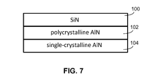
- FIG. 7 shows a diagram of a gate insulator stack in accordance with the present disclosure.
- FIG. 1 shows a diagram of III-nitride field effect transistor (FET) in accordance with the present disclosure.
- the FET has a buffer layer 14 formed on a substrate 12 .
- a channel layer 16 is formed on the buffer layer 14 and a barrier layer 18 , is formed on the channel layer 16 .
- the substrate 12 material may be silicon (Si), silicon carbide (SiC), sapphire (Al 2 O 3 ), gallium nitride (GaN), or aluminum nitride (AlN).
- the buffer layer 14 may be a stack of III-Nitride materials grown on the substrate 12 by chemical vapor deposition or molecular beam epitaxy.
- the channel layer 16 may be a III-Nitride material, such as GaN, grown on the buffer layer 14 by chemical vapor deposition or molecular beam epitaxy. Typically the channel layer 16 is an undoped GaN layer with the thickness ranging from 5 nanometers to a few micrometers.
- the barrier layer 18 may be 1-30 nanometers thick and may typically be only 5 nm thick.
- the barrier layer 18 may be AlGaN, with a 25% Al composition.
- a source electrode 20 and a drain electrode 22 are in contact with the channel layer 16 and extend through the the barrier layer 18 .
- the source electrode 20 and drain electrode 22 are on opposite ends of the channel layer 16 .
- a dielectric layer 30 which may be 1 nm to 100 nm thick and is typically 10 nm thick, and which may be SiN, is deposited by metal organic chemical vapor deposition (MOCVD) on top of the AlGaN barrier layer 18 .
- MOCVD metal organic chemical vapor deposition
- the dielectric layer 30 is deposited by MOCVD at a temperature higher than 600 degrees C., and typically at 900 degrees C.
- the dielectric layer 30 is patterned to be on top of the AlGaN barrier layer 18 in a gate area for a distance of Ls 2 , Ls 1 , Lg, Ld 1 and Ld 2 , as shown in FIG. 1 , between the source 20 and drain 22 . In the embodiment of FIG. 1 , the dielectric layer 30 is not in contact with either the source 20 or the drain 22 .
- a first gate trench 32 with a length of Lg, as shown in FIG. 1 is formed through the dielectric layer 30 and the barrier layer 18 .
- the bottom 38 of the gate trench 32 is located within the channel layer 16 , and extends below the barrier layer 18 and into the channel layer 16 by a vertical distance 36 .
- This vertical distance 36 is between an interface of the barrier layer 18 and channel layer 16 and the bottom 38 of the gate trench 32 , and is typically between 0 and 10 nanometers (nm).
- the vertical distance 36 needs to be equal or greater than 0 nm for normally-off operation, and needs to be as small as possible to in order to minimize the on-resistance.
- a gate insulator 33 is formed in the gate trench 32 and over the dielectric layer 30 .
- the gate insulator 33 may include a stack of: a layer of single-crystalline AlN 104 at the bottom of the gate trench 32 , which may be up to 2 nm thick and typically 1 nm thick; a layer of polycrystalline AlN 102 on the single crystalline AlN layer, which is 1 nm to 50 nm thick and typically 10 nm thick; and an insulating layer of SiN 100 , which may be 1 nm to 50 nm thick and typically 10 nm thick, formed on the polycrystalline AlN layer.
- the single crystalline AlN 104 is preferably grown at a temperature greater than 600 C, and less than 1100 C.
- a preferred temperature for growing the single crystalline AlN 104 is 900 C.
- the poly crystalline AlN 102 is preferably grown at a temperature greater than 300 C, and less than 900 C, and a preferred temperature is 600 C.
- the gate insulator 33 stack makes the FET a normally off FET. Under a positive gate bias the FET has a very low gate leakage, and a high-mobility electron channel is formed at the interface between the barrier layer 18 and the channel layer 16 .
- the single-crystalline AlN layer 104 of the gate insulator stack 33 provides a high-quality interface for electron transport in the channel layer 16 . Furthermore, the single crystalline AlN layer 104 provides an energy barrier to prevent electron trapping into the polycrystalline AlN layer 102 .
- the thickness of the single crystalline AlN layer 104 is chosen to be thin enough, typically below 2 nm, to avoid accumulation of channel electrons in absence of a positive gate bias.
- the SiN layer 100 serves as a blocking layer to leakage paths through grain boundaries of the polycrystalline AlN layer 102 .
- the gate insulator 33 is formed in the trench 32 and over the dielectric layer 30 .
- the gate insulator 33 and the dielectric layer 30 are removed in regions beyond the gate area of Ls 2 , Ls 1 , Lg, Ld 1 and Ld 2 , as shown in FIG. 1 .
- a passivation dielectric 34 which may be SiN and have a thickness of 10 nm to 500 nm with a typical thickness of 100 nm, is deposited by plasma-enhanced chemical vapor deposition (PECVD) over the barrier layer 18 between the source 20 and the drain 22 , over the gate insulator 33 in the trench 32 , and over the gate insulator 33 on the dielectric layer 30 .
- PECVD plasma-enhanced chemical vapor deposition
- the passivation dielectric 34 is deposited by PECVD at a temperature lower than 500 degrees C., and typically at 300 degrees C.
- a second gate trench 40 is formed in passivation dielectric 34 by etching and may have a length of the sum of Lg, Ls 1 and Ld 1 , as shown in FIG. 1 .
- the second gate trench 40 extends to the gate insulator 33 in the gate trench 32 and overlaps the gate insulator 33 on the dielectric layer 30 by a distance Ls 1 and Ld 1 , as shown in FIG. 1 .
- the gate insulator 33 on the dielectric layer 30 for distance Ls 2 and Ld 2 on either side of Ls 1 and Ld 1 , as shown in FIG. 1 remains covered by the passivation layer 34 .
- a gate electrode 24 is formed within the second gate trench 40 and may extend over the passivation layer 34 partially toward the source electrode 20 by a distance Ls 3 , as shown in FIG. 1 , and partially toward the drain electrode 22 by a distance Ld 3 , as shown in FIG. 1 , to form an integrated gate field-plate.
- the gate electrode 24 may be any suitable metal.
- a dielectric layer 30 which may be a SiN layer deposited by metal organic chemical vapor deposition (MOCVD)
- MOCVD metal organic chemical vapor deposition
- PECVD plasma-enhanced chemical vapor deposition
- Dielectric layer 30 is deposited prior to the deposition of the gate insulator layer stack 33 .
- the dielectric layer 30 serves as a etch stop layer for the patterning of the gate insulator layer stack 33 , and dielectric layer 30 can survive subsequent high-temperature steps, such as the deposition of gate insulator layer stack 33 and the alloying of source 20 and drain 22 contacts.
- Dielectric layer 34 serves the purpose of mitigating trapping behaviors. Dielectric layer 34 is deposited after the deposition of gate insulator layer stack 33 , to avoid the impact of high-temperature processing on the properties of dielectric layer 34 .
- FIG. 2 shows a typical off-state current voltage (IV) characteristic of a FET in accordance with the present disclosure. As shown in FIG. 2 , the off-state current is very low even at 600 volts, demonstrating the breakdown voltage is greater than 600 volts.
- FIG. 3 shows a typical dynamic current voltage (IV) characteristic of a FET in accordance with the present disclosure, and the graph demonstrates that the on-resistance for a FET is only minimally degraded.
- FIG. 4 shows a diagram of another field effect transistor in accordance with the present disclosure.
- the embodiment of FIG. 4 is similar to the embodiment of FIG. 1 .
- the dielectric layer 30 which may be 1 nm to 100 nm thick and is typically 10 nm thick, and which may be SiN, is deposited by metal organic chemical vapor deposition (MOCVD) on top of the AlGaN barrier layer 18 and extends from the source 20 to the drain 22 , as shown in FIG. 4 , rather than just in the gate area as shown in FIG. 1 .
- MOCVD metal organic chemical vapor deposition
- FIG. 5 shows a diagram of yet another field effect transistor in accordance with the present disclosure.
- the embodiment of FIG. 5 is similar to the embodiment of FIG. 4 .
- the gate insulator stack 33 extends from the source 20 to the drain 22 , as shown in FIG. 5 , rather than just in the gate area as shown in FIG. 4 .
- FIG. 6 shows a diagram of still another field effect transistor in accordance with the present disclosure.
- the embodiment of FIG. 6 is similar to the embodiment of FIG. 1 .
- the bottom 38 of the gate trench 32 is located within the barrier layer 18 , and does not extend below the barrier layer 18 into the channel layer 16 .
- the gate trench 32 may also be only to the top surface of the barrier layer 18 .
- Variations of the embodiment of FIG. 6 may also include an embodiment where the dielectric layer 30 extends from the source 20 to the drain 22 , and another embodiment where both the dielectric layer 30 and the gate insulator stand extend from the source 20 to the drain 22 .
Abstract
Description
Claims (30)
Priority Applications (5)
| Application Number | Priority Date | Filing Date | Title |
|---|---|---|---|
| US14/290,029 US9337332B2 (en) | 2012-04-25 | 2014-05-29 | III-Nitride insulating-gate transistors with passivation |
| CN201480052849.1A CN105580140B (en) | 2013-09-30 | 2014-09-16 | Field-effect transistor and method |
| EP14847483.6A EP3053196B1 (en) | 2013-09-30 | 2014-09-16 | Field effect transistor and method |
| PCT/US2014/055881 WO2015047797A1 (en) | 2013-09-30 | 2014-09-16 | Field effect transistor and method |
| US15/345,406 US10276712B2 (en) | 2014-05-29 | 2016-11-07 | III-nitride field-effect transistor with dual gates |
Applications Claiming Priority (3)
| Application Number | Priority Date | Filing Date | Title |
|---|---|---|---|
| US13/456,039 US8853709B2 (en) | 2011-07-29 | 2012-04-25 | III-nitride metal insulator semiconductor field effect transistor |
| US14/041,667 US8941118B1 (en) | 2011-07-29 | 2013-09-30 | Normally-off III-nitride transistors with high threshold-voltage and low on-resistance |
| US14/290,029 US9337332B2 (en) | 2012-04-25 | 2014-05-29 | III-Nitride insulating-gate transistors with passivation |
Publications (2)
| Publication Number | Publication Date |
|---|---|
| US20150349117A1 US20150349117A1 (en) | 2015-12-03 |
| US9337332B2 true US9337332B2 (en) | 2016-05-10 |
Family
ID=52744354
Family Applications (1)
| Application Number | Title | Priority Date | Filing Date |
|---|---|---|---|
| US14/290,029 Active US9337332B2 (en) | 2012-04-25 | 2014-05-29 | III-Nitride insulating-gate transistors with passivation |
Country Status (2)
| Country | Link |
|---|---|
| US (1) | US9337332B2 (en) |
| WO (1) | WO2015047797A1 (en) |
Cited By (18)
| Publication number | Priority date | Publication date | Assignee | Title |
|---|---|---|---|---|
| US20170148906A1 (en) * | 2015-11-24 | 2017-05-25 | Stmicroelectronics S.R.L. | Normally-off transistor with reduced on-state resistance and manufacturing method |
| US9812532B1 (en) | 2015-08-28 | 2017-11-07 | Hrl Laboratories, Llc | III-nitride P-channel transistor |
| US20170373176A1 (en) * | 2016-06-24 | 2017-12-28 | Cree Fayetteville, Inc. | Gallium nitride high-electron mobility transistors with p-type layers and process for making the same |
| US10192980B2 (en) | 2016-06-24 | 2019-01-29 | Cree, Inc. | Gallium nitride high-electron mobility transistors with deep implanted p-type layers in silicon carbide substrates for power switching and radio frequency applications and process for making the same |
| US10276712B2 (en) | 2014-05-29 | 2019-04-30 | Hrl Laboratories, Llc | III-nitride field-effect transistor with dual gates |
| US10522670B2 (en) | 2012-06-26 | 2019-12-31 | Nxp Usa, Inc. | Semiconductor device with selectively etched surface passivation |
| US10692984B2 (en) | 2015-11-19 | 2020-06-23 | Hrl Laboratories, Llc | III-nitride field-effect transistor with dual gates |
| US10825924B2 (en) | 2012-06-26 | 2020-11-03 | Nxp Usa, Inc. | Semiconductor device with selectively etched surface passivation |
| US10840334B2 (en) | 2016-06-24 | 2020-11-17 | Cree, Inc. | Gallium nitride high-electron mobility transistors with deep implanted p-type layers in silicon carbide substrates for power switching and radio frequency applications and process for making the same |
| US20200373421A1 (en) * | 2019-05-22 | 2020-11-26 | Intel Corporation | Iii-n transistor arrangements for reducing nonlinearity of off-state capacitance |
| US10892356B2 (en) | 2016-06-24 | 2021-01-12 | Cree, Inc. | Group III-nitride high-electron mobility transistors with buried p-type layers and process for making the same |
| US10957790B2 (en) | 2012-06-26 | 2021-03-23 | Nxp Usa, Inc. | Semiconductor device with selectively etched surface passivation |
| US10964802B2 (en) | 2018-07-23 | 2021-03-30 | Kabushiki Kaisha Toshiba | Semiconductor device and method for manufacturing the same |
| US11088269B2 (en) | 2019-06-28 | 2021-08-10 | Kabushiki Kaisha Toshiba | Semiconductor device |
| US11139393B2 (en) | 2019-03-14 | 2021-10-05 | Kabushiki Kaisha Toshiba | Semiconductor device including different nitride regions and method for manufacturing same |
| US20210320197A1 (en) * | 2020-04-09 | 2021-10-14 | Qualcomm Incorporated | MULTI-GATE HIGH ELECTRON MOBILITY TRANSISTORS (HEMTs) EMPLOYING TUNED RECESS DEPTH GATES FOR IMPROVED DEVICE LINEARITY |
| US11929428B2 (en) | 2021-05-17 | 2024-03-12 | Wolfspeed, Inc. | Circuits and group III-nitride high-electron mobility transistors with buried p-type layers improving overload recovery and process for implementing the same |
| US11967641B2 (en) | 2019-03-14 | 2024-04-23 | Kabushiki Kaisha Toshiba | Semiconductor device including different nitride regions improving characteristics of the semiconductor device |
Families Citing this family (12)
| Publication number | Priority date | Publication date | Assignee | Title |
|---|---|---|---|---|
| US9633920B2 (en) * | 2015-02-12 | 2017-04-25 | Taiwan Semiconductor Manufacturing Co., Ltd. | Low damage passivation layer for III-V based devices |
| EP3284107B1 (en) * | 2015-04-14 | 2023-06-14 | Hrl Laboratories, Llc | Iii-nitride transistor with trench gate |
| JP2017168768A (en) * | 2016-03-18 | 2017-09-21 | 三菱電機株式会社 | Field-effect transistor and method of manufacturing the same |
| EP3252825B1 (en) * | 2016-05-30 | 2022-12-21 | STMicroelectronics S.r.l. | Double-channel hemt device and manufacturing method thereof |
| JP6868389B2 (en) * | 2016-12-27 | 2021-05-12 | 住友化学株式会社 | Semiconductor substrates and electronic devices |
| WO2018234338A1 (en) * | 2017-06-19 | 2018-12-27 | Epigan Nv | A high electron mobility transistor |
| US10707322B2 (en) * | 2018-10-22 | 2020-07-07 | Vanguard International Semiconductor Corporation | Semiconductor devices and methods for fabricating the same |
| US11757027B2 (en) * | 2018-12-13 | 2023-09-12 | Intel Corporation | E-D mode 2DEG FET with gate spacer to locally tune VT and improve breakdown |
| US10818787B1 (en) | 2019-04-18 | 2020-10-27 | Semiconductor Components Industries, Llc | Electronic device including a high electron mobility transistor including a gate electrode and a dielectric film |
| EP3973576A1 (en) * | 2019-05-23 | 2022-03-30 | Power Integrations, Inc. | An enhancement mode metal insulator semiconductor high electron mobility transistor |
| US11955522B2 (en) * | 2020-02-13 | 2024-04-09 | Vanguard International Semiconductor Corporation | Semiconductor structure and method of forming the same |
| US11848402B2 (en) * | 2020-03-11 | 2023-12-19 | Lumileds Llc | Light emitting diode devices with multilayer composite film including current spreading layer |
Citations (34)
| Publication number | Priority date | Publication date | Assignee | Title |
|---|---|---|---|---|
| US6423645B1 (en) | 2000-03-27 | 2002-07-23 | Mosel Vitelic Inc. | Method for forming a self-aligned contact |
| US20030020092A1 (en) | 2001-07-24 | 2003-01-30 | Primit Parikh | Insulating gate AlGaN/GaN HEMT |
| US20050056893A1 (en) | 2003-07-18 | 2005-03-17 | Peyman Hadizad | Vertical compound semiconductor field effect transistor structure |
| US20060060871A1 (en) | 2004-01-23 | 2006-03-23 | International Rectifier Corp. | Enhancement mode III-nitride FET |
| US20060194379A1 (en) | 2003-07-28 | 2006-08-31 | Jun Suda | Field effect transistor and method for manufacturing same |
| WO2007062589A1 (en) | 2005-11-29 | 2007-06-07 | The Hong Kong University Of Science And Technology | MONOLITHIC INTEGRATION OF ENHANCEMENT- AND DEPLETION-MODE AlGaN/GaN HFETS |
| US20070141823A1 (en) | 2005-12-12 | 2007-06-21 | Kyma Technologies, Inc. | Inclusion-free uniform semi-insulating group III nitride substrates and methods for making same |
| US20070210332A1 (en) | 2005-01-14 | 2007-09-13 | Matsushita Electric Industrial Co., Ltd. | Semiconductor device |
| US7304331B2 (en) | 2004-07-14 | 2007-12-04 | Kabushiki Kaisha Toshiba | Nitride semiconductor device such as transverse power FET for high frequency signal amplification or power control |
| US20080121895A1 (en) * | 2006-11-06 | 2008-05-29 | Cree, Inc. | Methods of fabricating semiconductor devices including implanted regions for providing low-resistance contact to buried layers and related devices |
| JP2008227501A (en) | 2007-03-12 | 2008-09-25 | Cree Inc | Cap layer including aluminum nitride for nitride-based transistor, and method of fabricating the same |
| US20080237605A1 (en) | 2007-03-29 | 2008-10-02 | Tomohiro Murata | Semiconductor device and manufacturing method of the same |
| US20080261378A1 (en) | 2005-04-04 | 2008-10-23 | Tohoku Techno Arch Co., Ltd. | Method for Growth of Gan Single Crystal, Method for Preparation of Gan Substrate, Process for Producing Gan-Based Element, and Gan-Based Element |
| US20090146186A1 (en) | 2007-12-07 | 2009-06-11 | The Government of the United State of America, as represented by the Secretary of the Navy | Gate after Diamond Transistor |
| US7555219B2 (en) | 2003-07-14 | 2009-06-30 | Photonic Systems, Inc. | Bi-directional signal interface |
| US20100025730A1 (en) | 2008-07-31 | 2010-02-04 | Cree, Inc. | Normally-off Semiconductor Devices and Methods of Fabricating the Same |
| US20100090251A1 (en) | 2006-11-21 | 2010-04-15 | Interuniversitair Microelektronica Centrum (Imec) | SURFACE TREATMENT AND PASSIVATION OF AIGaN/GaN HEMT |
| US20100155780A1 (en) | 2008-12-22 | 2010-06-24 | Sanken Electric Co., Ltd. | Semiconductor device |
| US20110049526A1 (en) * | 2009-08-28 | 2011-03-03 | Transphorm Inc. | Semiconductor Devices with Field Plates |
| US8124505B1 (en) | 2010-10-21 | 2012-02-28 | Hrl Laboratories, Llc | Two stage plasma etching method for enhancement mode GaN HFET |
| JP2012156164A (en) | 2011-01-21 | 2012-08-16 | Toyota Central R&D Labs Inc | Semiconductor device |
| US20120261720A1 (en) | 2011-04-15 | 2012-10-18 | Stmicroelectronics S.R.I. | Method for manufacturing a hemt transistor and corresponding hemt transistor |
| US20130001646A1 (en) | 2011-06-29 | 2013-01-03 | Hrl Laboratories, Llc | ALGaN/GaN HYBRID MOS-HFET |
| US20130026495A1 (en) | 2011-07-29 | 2013-01-31 | Hrl Loboratories, Llc | III-Nitride Metal Insulator Semiconductor Field effect Transistor |
| US20130092947A1 (en) * | 2011-10-14 | 2013-04-18 | Bruce M. Green | Semiconductor device and method of making |
| US20130181224A1 (en) | 2009-09-15 | 2013-07-18 | Fraunhofer-Gesellschaft Zur Foerderung Der Angewandten Forschung E.V. | Semiconductor structure |
| US20130306978A1 (en) * | 2012-05-17 | 2013-11-21 | The Hong Kong University Of Science And Technology | Passivation of group iii-nitride heterojunction devices |
| US20130313609A1 (en) * | 2012-05-24 | 2013-11-28 | Rohm Co., Ltd. | Nitride semiconductor device and manufacturing method thereof |
| US20140092396A1 (en) | 2012-09-28 | 2014-04-03 | Sick Stegmann Gmbh | Device for measuring the relative position of two objects moving in relation to each other |
| US20140159050A1 (en) * | 2012-12-12 | 2014-06-12 | Electronics And Telecommunications Research Institute | Field effect transistor and method of fabricating the same |
| US20140191288A1 (en) * | 2013-01-09 | 2014-07-10 | Fujitsu Semiconductor Limited | Semiconductor device and method for manufacturing semiconductor device |
| US8941118B1 (en) | 2011-07-29 | 2015-01-27 | Hrl Laboratories, Llc | Normally-off III-nitride transistors with high threshold-voltage and low on-resistance |
| US20150048419A1 (en) * | 2013-08-15 | 2015-02-19 | Renesas Electronics Corporation | Semiconductor device and method of manufacturing the same |
| US20150060946A1 (en) * | 2013-08-27 | 2015-03-05 | Fujitsu Limited | Compound semiconductor device and method of manufacturing the same |
-
2014
- 2014-05-29 US US14/290,029 patent/US9337332B2/en active Active
- 2014-09-16 WO PCT/US2014/055881 patent/WO2015047797A1/en active Application Filing
Patent Citations (42)
| Publication number | Priority date | Publication date | Assignee | Title |
|---|---|---|---|---|
| US6423645B1 (en) | 2000-03-27 | 2002-07-23 | Mosel Vitelic Inc. | Method for forming a self-aligned contact |
| US20030020092A1 (en) | 2001-07-24 | 2003-01-30 | Primit Parikh | Insulating gate AlGaN/GaN HEMT |
| US20090315078A1 (en) | 2001-07-24 | 2009-12-24 | Cree, Inc. | INSULATING GATE AlGaN/GaN HEMT |
| US7555219B2 (en) | 2003-07-14 | 2009-06-30 | Photonic Systems, Inc. | Bi-directional signal interface |
| US20050056893A1 (en) | 2003-07-18 | 2005-03-17 | Peyman Hadizad | Vertical compound semiconductor field effect transistor structure |
| US20060194379A1 (en) | 2003-07-28 | 2006-08-31 | Jun Suda | Field effect transistor and method for manufacturing same |
| US7622763B2 (en) | 2003-07-28 | 2009-11-24 | Japan Science And Technology Agency | Field effect transistor and method for manufacturing same |
| US20060060871A1 (en) | 2004-01-23 | 2006-03-23 | International Rectifier Corp. | Enhancement mode III-nitride FET |
| US7304331B2 (en) | 2004-07-14 | 2007-12-04 | Kabushiki Kaisha Toshiba | Nitride semiconductor device such as transverse power FET for high frequency signal amplification or power control |
| US20070210332A1 (en) | 2005-01-14 | 2007-09-13 | Matsushita Electric Industrial Co., Ltd. | Semiconductor device |
| US20080261378A1 (en) | 2005-04-04 | 2008-10-23 | Tohoku Techno Arch Co., Ltd. | Method for Growth of Gan Single Crystal, Method for Preparation of Gan Substrate, Process for Producing Gan-Based Element, and Gan-Based Element |
| WO2007062589A1 (en) | 2005-11-29 | 2007-06-07 | The Hong Kong University Of Science And Technology | MONOLITHIC INTEGRATION OF ENHANCEMENT- AND DEPLETION-MODE AlGaN/GaN HFETS |
| US20070141823A1 (en) | 2005-12-12 | 2007-06-21 | Kyma Technologies, Inc. | Inclusion-free uniform semi-insulating group III nitride substrates and methods for making same |
| US20080121895A1 (en) * | 2006-11-06 | 2008-05-29 | Cree, Inc. | Methods of fabricating semiconductor devices including implanted regions for providing low-resistance contact to buried layers and related devices |
| US20100090251A1 (en) | 2006-11-21 | 2010-04-15 | Interuniversitair Microelektronica Centrum (Imec) | SURFACE TREATMENT AND PASSIVATION OF AIGaN/GaN HEMT |
| JP2008227501A (en) | 2007-03-12 | 2008-09-25 | Cree Inc | Cap layer including aluminum nitride for nitride-based transistor, and method of fabricating the same |
| US20080237605A1 (en) | 2007-03-29 | 2008-10-02 | Tomohiro Murata | Semiconductor device and manufacturing method of the same |
| US20090146186A1 (en) | 2007-12-07 | 2009-06-11 | The Government of the United State of America, as represented by the Secretary of the Navy | Gate after Diamond Transistor |
| US8592868B2 (en) | 2008-07-31 | 2013-11-26 | Cree, Inc. | Normally-off semiconductor devices |
| US20100025730A1 (en) | 2008-07-31 | 2010-02-04 | Cree, Inc. | Normally-off Semiconductor Devices and Methods of Fabricating the Same |
| US20120235160A1 (en) | 2008-07-31 | 2012-09-20 | Sten Heikman | Normally-Off Semiconductor Devices |
| US20100155780A1 (en) | 2008-12-22 | 2010-06-24 | Sanken Electric Co., Ltd. | Semiconductor device |
| US20110049526A1 (en) * | 2009-08-28 | 2011-03-03 | Transphorm Inc. | Semiconductor Devices with Field Plates |
| US20130181224A1 (en) | 2009-09-15 | 2013-07-18 | Fraunhofer-Gesellschaft Zur Foerderung Der Angewandten Forschung E.V. | Semiconductor structure |
| US8872233B2 (en) | 2009-09-15 | 2014-10-28 | Fraunhofer-Gesellschaft Zur Foerderung Der Angewandten Forschung E.V. | Semiconductor structure |
| US9059200B1 (en) | 2010-10-21 | 2015-06-16 | Hrl Laboratories, Llc | III-Nitride metal-insulator-semiconductor field-effect transistor |
| US8124505B1 (en) | 2010-10-21 | 2012-02-28 | Hrl Laboratories, Llc | Two stage plasma etching method for enhancement mode GaN HFET |
| JP2012156164A (en) | 2011-01-21 | 2012-08-16 | Toyota Central R&D Labs Inc | Semiconductor device |
| US20120261720A1 (en) | 2011-04-15 | 2012-10-18 | Stmicroelectronics S.R.I. | Method for manufacturing a hemt transistor and corresponding hemt transistor |
| US9024357B2 (en) | 2011-04-15 | 2015-05-05 | Stmicroelectronics S.R.L. | Method for manufacturing a HEMT transistor and corresponding HEMT transistor |
| US20130001646A1 (en) | 2011-06-29 | 2013-01-03 | Hrl Laboratories, Llc | ALGaN/GaN HYBRID MOS-HFET |
| US20130026495A1 (en) | 2011-07-29 | 2013-01-31 | Hrl Loboratories, Llc | III-Nitride Metal Insulator Semiconductor Field effect Transistor |
| US8853709B2 (en) | 2011-07-29 | 2014-10-07 | Hrl Laboratories, Llc | III-nitride metal insulator semiconductor field effect transistor |
| US8941118B1 (en) | 2011-07-29 | 2015-01-27 | Hrl Laboratories, Llc | Normally-off III-nitride transistors with high threshold-voltage and low on-resistance |
| US20130092947A1 (en) * | 2011-10-14 | 2013-04-18 | Bruce M. Green | Semiconductor device and method of making |
| US20130306978A1 (en) * | 2012-05-17 | 2013-11-21 | The Hong Kong University Of Science And Technology | Passivation of group iii-nitride heterojunction devices |
| US20130313609A1 (en) * | 2012-05-24 | 2013-11-28 | Rohm Co., Ltd. | Nitride semiconductor device and manufacturing method thereof |
| US20140092396A1 (en) | 2012-09-28 | 2014-04-03 | Sick Stegmann Gmbh | Device for measuring the relative position of two objects moving in relation to each other |
| US20140159050A1 (en) * | 2012-12-12 | 2014-06-12 | Electronics And Telecommunications Research Institute | Field effect transistor and method of fabricating the same |
| US20140191288A1 (en) * | 2013-01-09 | 2014-07-10 | Fujitsu Semiconductor Limited | Semiconductor device and method for manufacturing semiconductor device |
| US20150048419A1 (en) * | 2013-08-15 | 2015-02-19 | Renesas Electronics Corporation | Semiconductor device and method of manufacturing the same |
| US20150060946A1 (en) * | 2013-08-27 | 2015-03-05 | Fujitsu Limited | Compound semiconductor device and method of manufacturing the same |
Non-Patent Citations (45)
| Title |
|---|
| Ambacher, O. et al., "Two-Dimensional Electron Gases Induced by Spontaneous and Piezoelectric Polarization Charges in N- and Ga-face AlGaN/GaN Heterostructures," Journal of Applied Physics, vol. 85, No. 6, pp. 3222-3233, (Mar. 15, 1999). |
| Burnham, Shawn D. et al., "Gate-Recessed Normally-Off GaN-on-Si HEMT Using a New O2-BCl3 Digital Etching Technique," Physica Status Solidi C7, (ICNS-8), vol. 7, No. 7-8, pp. 2010-2012, (2010). |
| Buttari D. et al., "Digital Etching for Highly Reproducible Low Damage Gate Recessing on AlGaN/GaN HEMTs," Proceedings, IEEE Lester Eastman Conference, High Performance Devices, pp. 461-469, (Aug. 6-8, 2002). |
| Buttari D. et al., "Origin of Etch Delay Time in C12 Dry Etching of AlGaN/GaN Structures," Applied Physics Letters, vol. 83, No. 23, pp. 4779-4781, (Dec. 8, 2003). |
| Buttari D. et al., "Selective Dry Etching of GaN Over AlGaN in BCL3/SF6 Mixtures," Proceedings, IEEE Lester Eastman Conference, High Performance Devices, vol. 14, No. 3, pp. 132-137, (Aug. 2004). |
| Cai, Yong et al., "High-Performance Enhancement-Mode AlGaN/GaN HEMTs Using Fluoride-Based Plasma Treatment," IEEE Electron Device Letters, vol. 26, No. 7, pp. 435-437, (Jul. 2005). |
| Chapter II International Preliminary Report on Patentability (IPRP) for PCT/US2012/043114 mailed on Jul. 3, 2013. |
| Chen, T. et al., "AlGaN/GaN MIS HEMT with ALD Dielectric," Digest of CS MANTECH Conference, pp. 227-230, (Apr. 24-27, 2006). |
| Chp. II International Preliminary Report on Patentability (IPRP) for PCT/US2013/062750 mailed on Aug. 25, 2015. |
| DeSalvo, Gregory C. et al., "Wet Chemical Digital Etching of GaAs at Room Temperature," Journal of The Electrochemical Society, vol. 143, No. 11, pp. 3652-3656, (Nov. 1996). |
| EPO Extended Search Report with Search Opinion for European Patent Application No. 12819630.0 mailed on Mar. 6, 2015. |
| From U.S. Appl. No. 12/909,497 (Now U.S. Pat. No. 8,124,505), additional Non-Final Rejection mailed on May 31, 2011. |
| From U.S. Appl. No. 12/909,497 (Now U.S. Pat. No. 8,124,505), Non-Final Rejection mailed on May 31, 2011. |
| From U.S. Appl. No. 12/909,497 (Now U.S. Pat. No. 8,124,505), Notice of Allowance mailed on Nov. 10, 2011. |
| From U.S. Appl. No. 12/909,497 (Now U.S. Pat. No. 8,124,505), Notice of Allowance mailed on Oct. 24, 2011. |
| From U.S. Appl. No. 13/456,039 (Now U.S. Pat. No. 8,853,709), Advisory Action mailed on Sep. 6, 2013. |
| From U.S. Appl. No. 13/456,039 (Now U.S. Pat. No. 8,853,709), Final Rejection mailed on Jul. 12, 2013. |
| From U.S. Appl. No. 13/456,039 (Now U.S. Pat. No. 8,853,709), Non-Final Rejection mailed on Apr. 14, 2014. |
| From U.S. Appl. No. 13/456,039 (Now U.S. Pat. No. 8,853,709), Non-Final Rejection mailed on Apr. 3, 2013. |
| From U.S. Appl. No. 13/456,039 (Now U.S. Pat. No. 8,853,709), Notice of Allowance mailed on Aug. 12, 2014. |
| From U.S. Appl. No. 13/456,039 (Now U.S. Pat. No. 8,853,709), Notice of Allowance mailed on Jun. 6, 2014. |
| From U.S. Appl. No. 13/456,039 (Now U.S. Pat. No. 8,853,709), Rejection/Election mailed on Mar. 22, 2013. |
| From U.S. Appl. No. 14/041,667 (Now U.S. Pat. No. 8,941,118), Notice of Allowance mailed on Sep. 19, 2014. |
| From U.S. Appl. No. 14/469,187 (Now U.S. Pat. No. 9,059,200), Non-Final Rejection mailed on Nov. 25, 2014. |
| From U.S. Appl. No. 14/469,187 (Now U.S. Pat. No. 9,059,200), Notice of Allowance mailed on Feb. 13, 2015. |
| From U.S. Appl. No. 14/469,187 (Now U.S. Pat. No. 9,059,200), Notice of Allowance mailed on May 11, 2015. |
| From U.S. Appl. No. 14/838,958 (Unpublished, Non Publication Requested, filed Aug. 28, 2015), Application and Office Actions. |
| Hahn et al., "P-Channel Enhancement and Depletion Mode GaN-Based HFETs with Quaternary Backbarriers," IEEE Transaction on Electron Devices, (2013). |
| Harris H. et al., "Plasma Enhanced Metalorganic Chemical Vapor Deposition of Amorphous Aluminum Nitrade," Journal of Applied Physics, American Institute of Physics, vol. 90, No. 11, pp. 5825-5831, (Dec. 1, 2011). |
| Hashizume, T. et al., "Capacitance-Voltage Characterization of AlN/GaN Metal-Insulator-Semiconductor Structures Grown on Sapphire Substrate by Metalorganic Chemical Vapor Deposition," Journal of Applied Physics, vol. 88, No. 4, pp. 1983-1986, (Aug. 15, 2000). |
| International Search Report and Written Opinion for PCT/US2012/043114 mailed on Dec. 26, 2012. |
| International Search Report and Written Opinion from PCT/US2014/055881 mailed Dec. 22, 2014. |
| ISR/WO for related PCT/US2013/062750 mailed on Jun. 26, 2014. |
| Keogh, David et al., "Digital Etching of III-N Materials Using a Two-Step Ar/KOH Technique," Journal of Electronic Materials, vol. 35, No. 4, pp. 771-776, (2006). |
| Khan, M. Asif et al., "Enhancement and Depletion Mode GaN/AlGaN Heterostructure Field Effect Transistors," Applied Physics Letters, vol. 68, No. 4, pp. 514-516, (Jan. 22, 1996). |
| Lanford, W. B. et al., "Recessed-gate enhancement-mode GaN HEMT with high threshold voltage," Electronics Letters, vol. 41, No. 7, pp. 449-450, (Mar. 31, 2005). |
| Li G. et al., "Polarization-Induced GaN on Insulator E/D Mode P-Channel Heterostructure FETs," IEEE Electron Device Letters, (2013). |
| Ludviksson, Audunn et al., "Atomic Layer Etching Chemistry of Cl2 on GaAs(100)," Surface Science, vol. 277, pp. 282-300, (1992). |
| Maher, H. et al., "Smooth Wet Etching by Ultraviolet-Assisted Photoetching and Its Application to the Fabrication of AlGaN/GaN Heterostructure Field-Effect Transistors," Applied Physics Letters, vol. 77, No. 23, pp. 3833-3835, (Dec. 4, 2000). |
| Moon, Jeong S. et al., "Submicron Enhancement-mode AlGaN/GaN HEMTs," Device Research Conference, 60th DRC. Conference Digest, pp. 23-24, (2002). |
| Okamoto Y. et al., "179 W Recessed-Gate AlGaN/GaN Heterojunction FET with Field-Modulating Plate," Electronics Letters, vol. 40, No. 10, (May 13, 2004). |
| Parish, G. et al., "Simple Wet Etching of GaN," Proceedings of SPIE, Device and Process Technologies for MEMS and Microelectronics II, vol. 4592, pp. 104-110, (2001). |
| Shatalov, M. et al., "GaN/AlGaN P-Channel Inverted Heterostructure JFET," IEEE Electron Device Letters, (2002). |
| U.S. Appl. No. 14/838,958, filed Aug. 28, 2015, Chu et al. |
| Zimmermann T. et al., "P-Channel InGaN HFET Structure Based on Polarization Doping," IEEE Electron Device Letters, (2004). |
Cited By (24)
| Publication number | Priority date | Publication date | Assignee | Title |
|---|---|---|---|---|
| US10957790B2 (en) | 2012-06-26 | 2021-03-23 | Nxp Usa, Inc. | Semiconductor device with selectively etched surface passivation |
| US10522670B2 (en) | 2012-06-26 | 2019-12-31 | Nxp Usa, Inc. | Semiconductor device with selectively etched surface passivation |
| US10825924B2 (en) | 2012-06-26 | 2020-11-03 | Nxp Usa, Inc. | Semiconductor device with selectively etched surface passivation |
| US10276712B2 (en) | 2014-05-29 | 2019-04-30 | Hrl Laboratories, Llc | III-nitride field-effect transistor with dual gates |
| US9812532B1 (en) | 2015-08-28 | 2017-11-07 | Hrl Laboratories, Llc | III-nitride P-channel transistor |
| US10692984B2 (en) | 2015-11-19 | 2020-06-23 | Hrl Laboratories, Llc | III-nitride field-effect transistor with dual gates |
| US20170148906A1 (en) * | 2015-11-24 | 2017-05-25 | Stmicroelectronics S.R.L. | Normally-off transistor with reduced on-state resistance and manufacturing method |
| US20220130990A1 (en) * | 2015-11-24 | 2022-04-28 | Stmicroelectronics S.R.L. | Normally-off transistor with reduced on-state resistance and manufacturing method |
| US11222969B2 (en) | 2015-11-24 | 2022-01-11 | Stmicroelectronics S.R.L. | Normally-off transistor with reduced on-state resistance and manufacturing method |
| US11430882B2 (en) * | 2016-06-24 | 2022-08-30 | Wolfspeed, Inc. | Gallium nitride high-electron mobility transistors with p-type layers and process for making the same |
| US10840334B2 (en) | 2016-06-24 | 2020-11-17 | Cree, Inc. | Gallium nitride high-electron mobility transistors with deep implanted p-type layers in silicon carbide substrates for power switching and radio frequency applications and process for making the same |
| US11862719B2 (en) | 2016-06-24 | 2024-01-02 | Wolfspeed, Inc. | Group III-nitride high-electron mobility transistors with buried p-type layers and process for making the same |
| US10892356B2 (en) | 2016-06-24 | 2021-01-12 | Cree, Inc. | Group III-nitride high-electron mobility transistors with buried p-type layers and process for making the same |
| US20170373176A1 (en) * | 2016-06-24 | 2017-12-28 | Cree Fayetteville, Inc. | Gallium nitride high-electron mobility transistors with p-type layers and process for making the same |
| US10192980B2 (en) | 2016-06-24 | 2019-01-29 | Cree, Inc. | Gallium nitride high-electron mobility transistors with deep implanted p-type layers in silicon carbide substrates for power switching and radio frequency applications and process for making the same |
| US10964802B2 (en) | 2018-07-23 | 2021-03-30 | Kabushiki Kaisha Toshiba | Semiconductor device and method for manufacturing the same |
| US11677020B2 (en) | 2019-03-14 | 2023-06-13 | Kabushiki Kaisha Toshiba | Semiconductor device including different nitride regions and method for manufacturing same |
| US11139393B2 (en) | 2019-03-14 | 2021-10-05 | Kabushiki Kaisha Toshiba | Semiconductor device including different nitride regions and method for manufacturing same |
| US11967641B2 (en) | 2019-03-14 | 2024-04-23 | Kabushiki Kaisha Toshiba | Semiconductor device including different nitride regions improving characteristics of the semiconductor device |
| US20200373421A1 (en) * | 2019-05-22 | 2020-11-26 | Intel Corporation | Iii-n transistor arrangements for reducing nonlinearity of off-state capacitance |
| US11088269B2 (en) | 2019-06-28 | 2021-08-10 | Kabushiki Kaisha Toshiba | Semiconductor device |
| US20210320197A1 (en) * | 2020-04-09 | 2021-10-14 | Qualcomm Incorporated | MULTI-GATE HIGH ELECTRON MOBILITY TRANSISTORS (HEMTs) EMPLOYING TUNED RECESS DEPTH GATES FOR IMPROVED DEVICE LINEARITY |
| US11855198B2 (en) * | 2020-04-09 | 2023-12-26 | Qualcomm Incorporated | Multi-gate high electron mobility transistors (HEMTs) employing tuned recess depth gates for improved device linearity |
| US11929428B2 (en) | 2021-05-17 | 2024-03-12 | Wolfspeed, Inc. | Circuits and group III-nitride high-electron mobility transistors with buried p-type layers improving overload recovery and process for implementing the same |
Also Published As
| Publication number | Publication date |
|---|---|
| WO2015047797A1 (en) | 2015-04-02 |
| US20150349117A1 (en) | 2015-12-03 |
Similar Documents
| Publication | Publication Date | Title |
|---|---|---|
| US9337332B2 (en) | III-Nitride insulating-gate transistors with passivation | |
| US8941118B1 (en) | Normally-off III-nitride transistors with high threshold-voltage and low on-resistance | |
| EP3055885B1 (en) | Normally-off iii-nitride transistors with high threshold-voltage and low on-resistance | |
| US10410868B2 (en) | Semiconductor device and method of manufacturing semiconductor device | |
| US9620599B2 (en) | GaN-based semiconductor transistor | |
| US9406792B2 (en) | Semiconductor device having GaN-based layer | |
| US10283632B2 (en) | Nitride semiconductor device and manufacturing method thereof | |
| US10096702B2 (en) | Multi-step surface passivation structures and methods for fabricating same | |
| US8962461B2 (en) | GaN HEMTs and GaN diodes | |
| US20120193637A1 (en) | Low gate-leakage structure and method for gallium nitride enhancement mode transistor | |
| US8969881B2 (en) | Power transistor having segmented gate | |
| US20090206373A1 (en) | Field effect transistor | |
| US10784361B2 (en) | Semiconductor device and method for manufacturing the same | |
| US10243049B2 (en) | Nitride semiconductor device | |
| JP5055737B2 (en) | Field effect transistor having a two-dimensional carrier gas layer | |
| WO2014129245A1 (en) | Nitride semiconductor device | |
| EP3053196B1 (en) | Field effect transistor and method | |
| US9640620B2 (en) | High power transistor with oxide gate barriers |
Legal Events
| Date | Code | Title | Description |
|---|---|---|---|
| AS | Assignment |
Owner name: HRL LABORATORIES LLC, CALIFORNIA Free format text: ASSIGNMENT OF ASSIGNORS INTEREST;ASSIGNORS:CHU, RONGMING;CHEN, MARY Y.;CHEN, XU;AND OTHERS;SIGNING DATES FROM 20140529 TO 20140709;REEL/FRAME:033358/0776 |
|
| STCF | Information on status: patent grant |
Free format text: PATENTED CASE |
|
| MAFP | Maintenance fee payment |
Free format text: PAYMENT OF MAINTENANCE FEE, 4TH YEAR, LARGE ENTITY (ORIGINAL EVENT CODE: M1551); ENTITY STATUS OF PATENT OWNER: LARGE ENTITY Year of fee payment: 4 |
|
| MAFP | Maintenance fee payment |
Free format text: PAYMENT OF MAINTENANCE FEE, 8TH YEAR, LARGE ENTITY (ORIGINAL EVENT CODE: M1552); ENTITY STATUS OF PATENT OWNER: LARGE ENTITY Year of fee payment: 8 |