EP1296377B1 - A method for fabricating a small area of contact between electrodes - Google Patents
A method for fabricating a small area of contact between electrodes Download PDFInfo
- Publication number
- EP1296377B1 EP1296377B1 EP02079437A EP02079437A EP1296377B1 EP 1296377 B1 EP1296377 B1 EP 1296377B1 EP 02079437 A EP02079437 A EP 02079437A EP 02079437 A EP02079437 A EP 02079437A EP 1296377 B1 EP1296377 B1 EP 1296377B1
- Authority
- EP
- European Patent Office
- Prior art keywords
- layer
- chalcogenide
- electrode
- conductive layer
- tip
- Prior art date
- Legal status (The legal status is an assumption and is not a legal conclusion. Google has not performed a legal analysis and makes no representation as to the accuracy of the status listed.)
- Expired - Lifetime
Links
- 238000000034 method Methods 0.000 title claims description 29
- 239000000463 material Substances 0.000 claims abstract description 53
- 150000004770 chalcogenides Chemical class 0.000 claims abstract description 48
- 230000015654 memory Effects 0.000 claims abstract description 42
- 238000005530 etching Methods 0.000 claims abstract description 12
- 238000004519 manufacturing process Methods 0.000 claims description 8
- 239000000758 substrate Substances 0.000 claims description 8
- 238000000151 deposition Methods 0.000 claims description 6
- 239000000203 mixture Substances 0.000 claims description 4
- 239000004065 semiconductor Substances 0.000 claims description 3
- 239000000126 substance Substances 0.000 claims description 3
- 238000005498 polishing Methods 0.000 claims 1
- 229910021420 polycrystalline silicon Inorganic materials 0.000 abstract description 17
- 229920005591 polysilicon Polymers 0.000 abstract description 17
- 239000010410 layer Substances 0.000 description 81
- VYPSYNLAJGMNEJ-UHFFFAOYSA-N Silicium dioxide Chemical compound O=[Si]=O VYPSYNLAJGMNEJ-UHFFFAOYSA-N 0.000 description 18
- 229910052814 silicon oxide Inorganic materials 0.000 description 18
- 239000011148 porous material Substances 0.000 description 14
- 239000004020 conductor Substances 0.000 description 13
- 238000007736 thin film deposition technique Methods 0.000 description 9
- 230000008569 process Effects 0.000 description 8
- 230000000873 masking effect Effects 0.000 description 7
- NRTOMJZYCJJWKI-UHFFFAOYSA-N Titanium nitride Chemical compound [Ti]#N NRTOMJZYCJJWKI-UHFFFAOYSA-N 0.000 description 6
- OKTJSMMVPCPJKN-UHFFFAOYSA-N Carbon Chemical compound [C] OKTJSMMVPCPJKN-UHFFFAOYSA-N 0.000 description 5
- 229910052799 carbon Inorganic materials 0.000 description 5
- 238000005229 chemical vapour deposition Methods 0.000 description 4
- 239000007772 electrode material Substances 0.000 description 4
- 238000010304 firing Methods 0.000 description 4
- 230000008021 deposition Effects 0.000 description 3
- -1 i.e. Substances 0.000 description 3
- 239000012782 phase change material Substances 0.000 description 3
- 229910052581 Si3N4 Inorganic materials 0.000 description 2
- XAGFODPZIPBFFR-UHFFFAOYSA-N aluminium Chemical compound [Al] XAGFODPZIPBFFR-UHFFFAOYSA-N 0.000 description 2
- 229910052782 aluminium Inorganic materials 0.000 description 2
- 238000003491 array Methods 0.000 description 2
- 230000008859 change Effects 0.000 description 2
- 239000000470 constituent Substances 0.000 description 2
- 230000000694 effects Effects 0.000 description 2
- 229920002120 photoresistant polymer Polymers 0.000 description 2
- 230000004044 response Effects 0.000 description 2
- 229910052710 silicon Inorganic materials 0.000 description 2
- 239000010703 silicon Substances 0.000 description 2
- HQVNEWCFYHHQES-UHFFFAOYSA-N silicon nitride Chemical compound N12[Si]34N5[Si]62N3[Si]51N64 HQVNEWCFYHHQES-UHFFFAOYSA-N 0.000 description 2
- 238000001228 spectrum Methods 0.000 description 2
- 238000003860 storage Methods 0.000 description 2
- 238000000427 thin-film deposition Methods 0.000 description 2
- ZOKXTWBITQBERF-UHFFFAOYSA-N Molybdenum Chemical compound [Mo] ZOKXTWBITQBERF-UHFFFAOYSA-N 0.000 description 1
- XUIMIQQOPSSXEZ-UHFFFAOYSA-N Silicon Chemical compound [Si] XUIMIQQOPSSXEZ-UHFFFAOYSA-N 0.000 description 1
- 230000015556 catabolic process Effects 0.000 description 1
- 239000003989 dielectric material Substances 0.000 description 1
- 239000011810 insulating material Substances 0.000 description 1
- 239000011229 interlayer Substances 0.000 description 1
- 239000011733 molybdenum Substances 0.000 description 1
- 229910052750 molybdenum Inorganic materials 0.000 description 1
- 150000004767 nitrides Chemical class 0.000 description 1
- 238000001020 plasma etching Methods 0.000 description 1
- 230000009467 reduction Effects 0.000 description 1
- 239000010936 titanium Substances 0.000 description 1
- WFKWXMTUELFFGS-UHFFFAOYSA-N tungsten Chemical compound [W] WFKWXMTUELFFGS-UHFFFAOYSA-N 0.000 description 1
- 229910052721 tungsten Inorganic materials 0.000 description 1
- 239000010937 tungsten Substances 0.000 description 1
Images

Classifications
-
- H—ELECTRICITY
- H01—ELECTRIC ELEMENTS
- H01L—SEMICONDUCTOR DEVICES NOT COVERED BY CLASS H10
- H01L21/00—Processes or apparatus adapted for the manufacture or treatment of semiconductor or solid state devices or of parts thereof
- H01L21/02—Manufacture or treatment of semiconductor devices or of parts thereof
- H01L21/04—Manufacture or treatment of semiconductor devices or of parts thereof the devices having potential barriers, e.g. a PN junction, depletion layer or carrier concentration layer
- H01L21/18—Manufacture or treatment of semiconductor devices or of parts thereof the devices having potential barriers, e.g. a PN junction, depletion layer or carrier concentration layer the devices having semiconductor bodies comprising elements of Group IV of the Periodic Table or AIIIBV compounds with or without impurities, e.g. doping materials
- H01L21/28—Manufacture of electrodes on semiconductor bodies using processes or apparatus not provided for in groups H01L21/20 - H01L21/268
-
- H—ELECTRICITY
- H10—SEMICONDUCTOR DEVICES; ELECTRIC SOLID-STATE DEVICES NOT OTHERWISE PROVIDED FOR
- H10B—ELECTRONIC MEMORY DEVICES
- H10B63/00—Resistance change memory devices, e.g. resistive RAM [ReRAM] devices
- H10B63/80—Arrangements comprising multiple bistable or multi-stable switching components of the same type on a plane parallel to the substrate, e.g. cross-point arrays
-
- H—ELECTRICITY
- H10—SEMICONDUCTOR DEVICES; ELECTRIC SOLID-STATE DEVICES NOT OTHERWISE PROVIDED FOR
- H10N—ELECTRIC SOLID-STATE DEVICES NOT OTHERWISE PROVIDED FOR
- H10N70/00—Solid-state devices having no potential barriers, and specially adapted for rectifying, amplifying, oscillating or switching
- H10N70/011—Manufacture or treatment of multistable switching devices
- H10N70/061—Shaping switching materials
- H10N70/063—Shaping switching materials by etching of pre-deposited switching material layers, e.g. lithography
-
- H—ELECTRICITY
- H10—SEMICONDUCTOR DEVICES; ELECTRIC SOLID-STATE DEVICES NOT OTHERWISE PROVIDED FOR
- H10N—ELECTRIC SOLID-STATE DEVICES NOT OTHERWISE PROVIDED FOR
- H10N70/00—Solid-state devices having no potential barriers, and specially adapted for rectifying, amplifying, oscillating or switching
- H10N70/011—Manufacture or treatment of multistable switching devices
- H10N70/061—Shaping switching materials
- H10N70/066—Shaping switching materials by filling of openings, e.g. damascene method
-
- H—ELECTRICITY
- H10—SEMICONDUCTOR DEVICES; ELECTRIC SOLID-STATE DEVICES NOT OTHERWISE PROVIDED FOR
- H10N—ELECTRIC SOLID-STATE DEVICES NOT OTHERWISE PROVIDED FOR
- H10N70/00—Solid-state devices having no potential barriers, and specially adapted for rectifying, amplifying, oscillating or switching
- H10N70/20—Multistable switching devices, e.g. memristors
- H10N70/231—Multistable switching devices, e.g. memristors based on solid-state phase change, e.g. between amorphous and crystalline phases, Ovshinsky effect
-
- H—ELECTRICITY
- H10—SEMICONDUCTOR DEVICES; ELECTRIC SOLID-STATE DEVICES NOT OTHERWISE PROVIDED FOR
- H10N—ELECTRIC SOLID-STATE DEVICES NOT OTHERWISE PROVIDED FOR
- H10N70/00—Solid-state devices having no potential barriers, and specially adapted for rectifying, amplifying, oscillating or switching
- H10N70/801—Constructional details of multistable switching devices
- H10N70/821—Device geometry
- H10N70/826—Device geometry adapted for essentially vertical current flow, e.g. sandwich or pillar type devices
-
- H—ELECTRICITY
- H10—SEMICONDUCTOR DEVICES; ELECTRIC SOLID-STATE DEVICES NOT OTHERWISE PROVIDED FOR
- H10N—ELECTRIC SOLID-STATE DEVICES NOT OTHERWISE PROVIDED FOR
- H10N70/00—Solid-state devices having no potential barriers, and specially adapted for rectifying, amplifying, oscillating or switching
- H10N70/801—Constructional details of multistable switching devices
- H10N70/841—Electrodes
- H10N70/8418—Electrodes adapted for focusing electric field or current, e.g. tip-shaped
-
- H—ELECTRICITY
- H10—SEMICONDUCTOR DEVICES; ELECTRIC SOLID-STATE DEVICES NOT OTHERWISE PROVIDED FOR
- H10N—ELECTRIC SOLID-STATE DEVICES NOT OTHERWISE PROVIDED FOR
- H10N70/00—Solid-state devices having no potential barriers, and specially adapted for rectifying, amplifying, oscillating or switching
- H10N70/801—Constructional details of multistable switching devices
- H10N70/881—Switching materials
- H10N70/882—Compounds of sulfur, selenium or tellurium, e.g. chalcogenides
- H10N70/8828—Tellurides, e.g. GeSbTe
-
- G—PHYSICS
- G11—INFORMATION STORAGE
- G11C—STATIC STORES
- G11C2213/00—Indexing scheme relating to G11C13/00 for features not covered by this group
- G11C2213/50—Resistive cell structure aspects
- G11C2213/52—Structure characterized by the electrode material, shape, etc.
Definitions
- the present invention relates generally to semiconductor fabrication techniques and, more particularly, to a method for fabricating a small contact area between an upper and lower electrode for use in phase changeable memory devices such as, for example, chalcogenide memory cells.
- phase change materials i.e., materials that can be electrically switched between generally amorphous and generally crystalline states or between different resistive states while in crystalline form, for electronic memory applications.
- phase change materials is disclosed, for example, in U.S. Patent No. 5,296,716 , in the names of Ovshinsky et al. U.S. Patent No. 5,296,716 is believed to indicate generally the state of the art, and to contain a discussion of the current theory of operation of chalcogenide materials.
- phase change materials can be electrically switched between a first structural state where the material is generally amorphous and a second structural state where the material has a generally crystalline local order.
- the material may also be electrically switched between different detectable states of local order across the entire spectrum between the completely amorphous and the completely crystalline states. That is, the switching of such material is not required to take place between completely amorphous and completely crystalline states, but rather, the material can be switched in incremental steps reflecting changes of local order to provide a "gray scale" represented by a multiplicity of conditions of local order spanning the spectrum from the completely amorphous state to the completely crystalline state.
- Chalcogenide material exhibits different electrical characteristics depending upon its state. For example, in its amorphous state the material exhibits lower electrical conductivity than it does in its crystalline state.
- the operation of chalcogenide memory cells requires that a region of the chalcogenide memory material, called the chalcogenide active region, be subjected to a current pulse typically with a current density between 10 5 and 10 7 amperes/cm 2 , to change the crystalline state of the chalcogenide material within the active region contained within a small pore. This current density may be accomplished by first creating a small opening in a dielectric material that is itself deposited onto a lower electrode material.
- a second dielectric layer typically of silicon nitride, is then deposited onto the dielectric layer into the opening.
- the second dielectric layer is typically about 4 x 10 -9 m (40 Angstroms) thick.
- the chalcogenide material is then deposited over the second dielectric and into the opening.
- An upper electrode material is then deposited over the chalcogenide material.
- Carbon is commonly used as the electrode material, although other materials have also been used, for example, molybdenum and titanium nitride.
- a conductive path is then provided from the chalcogenide material to the lower electrode material by forming a, pore in the second dielectric layer by a well-known firing process.
- Firing involves passing an initial high current pulse through the structure that passes through the chalcogenide material and then provides dielectric breakdown of the second dielectric layer, thereby providing a conductive path via the pore created through the memory cell. Electrically firing the thin nitride layer is not desirable for a high density memory product due to the high current required and the large amount of testing time required for the firing.
- the active regions of the chalcogenide memory cells within the pores are believed to change crystalline structure in response to applied voltage pulses of a wide range of magnitudes and pulse durations. These changes in crystalline structure alter the bulk resistance of the chalcogenide active region.
- the wide dynamic range of these devices, the linearity of their response, and lack of hysteresis provide these memory cells with multiple bit storage capabilities.
- pore dimensions i.e., diameter, thickness and volume
- chalcogenide composition e.g., signal pulse duration and signal pulse waveform shape
- chalcogenide composition e.g., chalcogenide composition, signal pulse duration and signal pulse waveform shape
- pore dimensions i.e., diameter, thickness and volume
- chalcogenide composition e.g., signal pulse duration and signal pulse waveform shape
- the energy input required to adjust the crystalline state of the chalcogenide active region of the memory cell is directly proportional to the dimensions of the minimum lateral dimension of the pore, e.g., smaller pore sizes result in smaller energy input requirements.
- Conventional chalcogenide memory cell fabrication techniques provide minimum lateral pore dimension, diameter or width of the pore, that is limited by the photolithographic size limit. This results in pore sizes having minimum lateral dimensions down to approximately 3.5x10 -7 m (0.35 microns). However, further reduction in pore size is desirable to achieve improved current density for writing to the memory cell.
- the present invention is directed at overcoming, or at least reducing the effects of, one or more of the problems set forth above.
- the invention comprises an integrated circuit memory device as claimed in Claim 1.
- the invention comprises a method of fabricating a conductive path in an integrated circuit as claimed in Claim 6.
- the present invention provides a method for fabricating a small contact area between electrodes of chalcogenide memory cells, such that the contact area provides minimum dimensions below the photolithographic limit, thereby reducing the required energy input to the chalcogenide active region in operation.
- the electrodes are further selected to provide material properties that permit enhanced control of the current passing through the chalcogenide memory cell.
- the memory cells may be made smaller to provide denser memory arrays, and the overall power requirements for the memory cells are minimized.
- a method of fabricating a small area of contact between electrodes of chalcogenide memories is presented that provides an area of contact with the lower electrode by the upper electrode, via the chalcogenide material, that is smaller than that presently provided using conventional photolithographic techniques.
- the preferred embodiment of the present invention provides a method of fabricating electrodes for chalcogenide memories in which a minimum area of contact of the lower electrode with the upper electrode is formed by creating a tip on the lower electrode. In this manner, the lower electrode having a minimum area of contact as small as 0.00785 ⁇ m 2 is obtained.
- the present preferred embodiment thus provides enhanced control of the current passing through the resulting chalcogenide memory, and thus, reduces the total current and energy input required to the chalcogenide active region in operation.
- the total current passing through the chalcogenide active region is two milliamps (mA).
- the current density required by the preferred embodiment is 1 x 10 6 A/cm 2 to 1 x 10 7 A/cm 2 .
- the preferred embodiment allows the memory cells to be made smaller and thus allow the production of denser memory arrays, and allows the overall power requirements for the memory cell to be minimized.
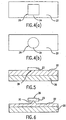
- a layer 22 of conductive material preferably polysilicon, is deposited onto a substrate 20 using conventional thin film deposition methods such as, for example, chemical vapor deposition (CVD), as illustrated in FIG. 1 .
- the layer 22 of conductive material may have a substantially uniform thickness ranging from 5 to 7 x 10 -7 m (5000 to 7000 Angstroms), and preferably will have a substantially uniform thickness of approximately 6.5 x 10 -7 m (6500) Angstroms.
- Substrate 20 may also be comprised of a conductive material such as, for example, silicon, TiN, Carbon, WiSi x , or Tungsten, and preferably will be comprised of silicon.
- the substrate 20 will further preferably comprise a lower electrode grid (not shown) used for accessing an array of chalcogenide memories.
- a layer 23 of silicon oxide is deposited onto the substrate 22, preferably by CVD, and preferably will have a thickness of 5 x 10 -8 m (500 Angstroms).
- a layer 24 of resist material is spun onto the silicon oxide layer 23, as illustrated in FIG. 2 .
- the layer 24 of resist material preferably will have a substantially uniform thickness of approximately 1.5 x 10 -6 m (15.000 Angstroms).
- a contact pattern 26, is then etched in the resist layer 24 and the silicon oxide layer 23 using conventional masking, exposing, etching, and photoresist stripping techniques as shown in FIG. 3 .
- the contact pattern 26 may be formed from the resist layer 24 and silicon oxide layer 23, for example, as a generally rectangular block as shown in FIG. 4(a) , or as a substantially circular block as shown in FIG. 4(b) .
- Contact pattern 26 is preferably formed using a conventional contact hole mask resulting in the substantially circular block shown in FIG. 4(b) .
- the minimum lateral dimension of the contact pattern 26 preferably will be approximately 0.4 ⁇ m.
- the contact pattern 26 includes a generally horizontal bottom surface 28, common to the polysilicon layer 22, and generally vertical side walls 27 at its outer periphery.
- the resist layer 24 is then removed using conventional stripping techniques after the contact 26 has been patterned in the silicon oxide layer 23, as shown in FIG. 5 .
- the silicon oxide layer 23 remains as the contact pattern 26.
- the silicon oxide layer 23 contact pattern is used as a masking layer when the polysilicon layer 22 is subsequently etched.
- the portion of the polysilicon layer 22 not covered by silicon oxide layer pattern 23 is etched, and the portions beneath silicon oxide pattern 23 are undercut, using wet etch or dry plasma etching techniques to form a frusto-conical shaped tip 30 in the polysilicon layer 22, as shown in FIG. 6 .
- the resulting tip 30 is frusto-conical in shape preferably having a minimum frustum lateral dimension of approximately 0.1 ⁇ m.
- the base of the tip 30 preferably will have a base minimum lateral dimension of approximately 0.4 ⁇ m, i.e., the same dimension as the lateral dimension of the contact pattern 26.
- Tip 30 will preferably have a height of approximately 2 x 10 -7 m (2000 Angstroms).
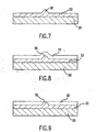
- the removal of the silicon oxide layer pattern 23 is accomplished using conventional wet etch techniques as shown in FIG. 7 .
- Contact pattern 26 thus provides a means for defining the area of contact of the base of the frusto-conical tip 30 of layer 22 of 0.00785 ⁇ m 2 [ ⁇ x (0.1/2) 2 ].
- a layer 32 of insulative material is deposited onto the polysilicon layer 22, including the tip 30, using conventional thin film deposition methods such as, for example, CVD, to isolate the polysilicon layer 22, including the tip 30, as illustrated in FIG. 8 .
- the layer 32 of insulative material may have a substantially uniform thickness of approximately 2 to 5 x 10 -7 m (2000 to 5000 Angstroms), and preferably will have a substantially uniform thickness of approximately 2 x 10 -7 m (2000 Angstroms), i.e., the same thickness as the height of the tip 30.
- Layer 32 of insulative material may be comprised of silicon oxide or silicon nitride, and preferably will be comprised of silicon oxide.
- the layer 32 of insulative material is then preferably planarized using a conventional chemical mechanical planarization (CMP) process as illustrated in FIG. 9 .
- CMP chemical mechanical planarization
- the CMP process is performed to expose the top surface 24 of the tip 30 formed on the polysilicon layer 22 that may also be referred to as the lower electrode.
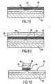
- the chalcogenide memory cell is then formed incorporating the tip 30 of the polysilicon layer 22 using conventional semiconductor processing techniques such as, for example, thin-film deposition, masking, and etching processes.
- the chalcogenide memory cell preferably includes a layer 34 of chalcogenide material, a layer 36 of conductive material serving as an upper electrode, an interlayer dielectric (ILD) layer 38, and an upper conductive layer 40.
- ILD interlayer dielectric
- the chalcogenide material layer 34 may be deposited using conventional thin film deposition methods as shown in FIG. 10 .
- Chalcogenide material layer 34 preferably is approximately 5 x 10 -8 m (500 Angstroms) thick.
- Typical chalcogenide compositions for these memory cells include average concentrations of Te in the amorphous state well below 70%, typically below about 60% and ranging in general from as low as about 23% up to about 56% Te, and most preferably to about 48% to 56% Te.
- Concentrations of Ge are typically above about 15 % and range from a low of about 17% to about 44% on average, and remain generally below 50% Ge, with the remainder of the principal constituent elements in this class being Sb. The percentages are atomic percentages which total 100% of the atoms of the constituent elements.
- the chalcogenide compositions for these memory cells comprise a Te concentration of about 56%, a Ge concentration of about 22%, and a Sb concentration of about 22%.
- the materials are typically characterized as Te a Ge b Sb 100-(a+b) , where a is equal to or less than about 70 % and preferably between about 40% to about 60%, b is above about 15% and less than 50%, and preferably between about 17% to 44%, and the remainder is Sb.
- the carbon layer 35 is preferably 6 x 10 -8 m (600 Angstroms) thick and is provided over the chalcogenide layer 34 using conventional thin film deposition techniques, as shown in FIG. 11 .
- Layer 36 of conductive material is deposited over the carbon layer 35 using conventional deposition techniques, as further shown in FIG. 11 .
- the layer 36 of conductive material thereby provides an upper electrode for the chalcogenide memory cell.
- the layer 36 of conductive material is preferably titanium nitride (TiN), but may comprise TiN or carbon, and has a thickness of approximately 5 x 10 -8 m (500 Angstroms).
- Layers 34-36 are subsequently etched back using conventional masking and etching techniques, as shown in FIG. 12 .
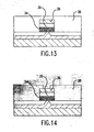
- the ILD layer 38 is then applied using conventional thin film deposition techniques.
- the ILD layer 38 preferably is approximately 3.5 x 10 -7 m (3500 Angstroms) thick, and comprises silicon oxide.
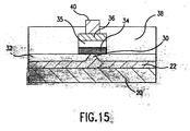
- the ILD layer 38 is then etched back, as shown in FIG. 14 , using conventional masking and etching processes to provide access to the layer 36 of conductive material or upper electrode by the upper conductive grid 40.
- Upper conductive grid interconnect 40 may be formed by first applying a blanket deposition of conductive material using conventional thin film deposition processes and then by etching the conductive material to form the upper conductive grid interconnect extending above the surface of the ILD layer 38, as shown in FIG. 15 .
- the upper conductive grid 40 material may comprise materials such as, for example, Ti, TiN, or aluminum, and preferably it will comprise aluminum.
- the methods described above are utilized to form an array of chalcogenide memory cells that are addressable by an X-Y grid of upper and lower conductors, i.e., electrodes.
- diodes are further provided in series with the chalcogenide memory cells to permit read/write operations from/to individual chalcogenide memory cells as will be recognized by persons of ordinary skill in the art.
- the present invention includes the fabrication of a plurality of tips 30 on the lower electrode, i.e., the polysilicon layer 22, such that a plurality of chalcogenide memory cells may be created.
- the drawings show only a single tip 30 for ease of illustration of the present invention.
- the particular materials selected for each layer must be selected to provide proper selectivity during the various etching processes as will be recognized by persons of ordinary skill in the art.
Landscapes
- Engineering & Computer Science (AREA)
- Manufacturing & Machinery (AREA)
- Microelectronics & Electronic Packaging (AREA)
- General Physics & Mathematics (AREA)
- Condensed Matter Physics & Semiconductors (AREA)
- Computer Hardware Design (AREA)
- Physics & Mathematics (AREA)
- Power Engineering (AREA)
- Semiconductor Memories (AREA)
- Electrical Discharge Machining, Electrochemical Machining, And Combined Machining (AREA)
- Surface Heating Bodies (AREA)
- Inert Electrodes (AREA)
- Electrodes Of Semiconductors (AREA)
- Contacts (AREA)
Applications Claiming Priority (3)
| Application Number | Priority Date | Filing Date | Title |
|---|---|---|---|
| US724816 | 1996-10-02 | ||
| US08/724,816 US6147395A (en) | 1996-10-02 | 1996-10-02 | Method for fabricating a small area of contact between electrodes |
| EP97955058A EP0946975B1 (en) | 1996-10-02 | 1997-10-02 | A device and method for fabricating a small area of contact between electrodes |
Related Parent Applications (1)
| Application Number | Title | Priority Date | Filing Date |
|---|---|---|---|
| EP97955058A Division EP0946975B1 (en) | 1996-10-02 | 1997-10-02 | A device and method for fabricating a small area of contact between electrodes |
Publications (3)
| Publication Number | Publication Date |
|---|---|
| EP1296377A2 EP1296377A2 (en) | 2003-03-26 |
| EP1296377A3 EP1296377A3 (en) | 2006-01-25 |
| EP1296377B1 true EP1296377B1 (en) | 2009-12-02 |
Family
ID=24912031
Family Applications (3)
| Application Number | Title | Priority Date | Filing Date |
|---|---|---|---|
| EP02079437A Expired - Lifetime EP1296377B1 (en) | 1996-10-02 | 1997-10-02 | A method for fabricating a small area of contact between electrodes |
| EP00202838A Expired - Lifetime EP1065736B1 (en) | 1996-10-02 | 1997-10-02 | A method for fabricating a small area of contact between electrodes |
| EP97955058A Expired - Lifetime EP0946975B1 (en) | 1996-10-02 | 1997-10-02 | A device and method for fabricating a small area of contact between electrodes |
Family Applications After (2)
| Application Number | Title | Priority Date | Filing Date |
|---|---|---|---|
| EP00202838A Expired - Lifetime EP1065736B1 (en) | 1996-10-02 | 1997-10-02 | A method for fabricating a small area of contact between electrodes |
| EP97955058A Expired - Lifetime EP0946975B1 (en) | 1996-10-02 | 1997-10-02 | A device and method for fabricating a small area of contact between electrodes |
Country Status (8)
| Country | Link |
|---|---|
| US (12) | US6147395A (ja) |
| EP (3) | EP1296377B1 (ja) |
| JP (1) | JP4747231B2 (ja) |
| KR (1) | KR100466675B1 (ja) |
| AT (3) | ATE248439T1 (ja) |
| AU (1) | AU8052598A (ja) |
| DE (3) | DE69739678D1 (ja) |
| WO (1) | WO1998036446A2 (ja) |
Families Citing this family (307)
| Publication number | Priority date | Publication date | Assignee | Title |
|---|---|---|---|---|
| US6147395A (en) | 1996-10-02 | 2000-11-14 | Micron Technology, Inc. | Method for fabricating a small area of contact between electrodes |
| US6617192B1 (en) * | 1997-10-01 | 2003-09-09 | Ovonyx, Inc. | Electrically programmable memory element with multi-regioned contact |
| US6969866B1 (en) * | 1997-10-01 | 2005-11-29 | Ovonyx, Inc. | Electrically programmable memory element with improved contacts |
| US6242304B1 (en) * | 1998-05-29 | 2001-06-05 | Micron Technology, Inc. | Method and structure for textured surfaces in floating gate tunneling oxide devices |
| US6943365B2 (en) * | 1999-03-25 | 2005-09-13 | Ovonyx, Inc. | Electrically programmable memory element with reduced area of contact and method for making same |
| CA2367365A1 (en) * | 1999-03-25 | 2000-09-28 | Stanford R. Ovshinsky | Electrically programmable memory element with improved contacts |
| US6750079B2 (en) * | 1999-03-25 | 2004-06-15 | Ovonyx, Inc. | Method for making programmable resistance memory element |
| US6391658B1 (en) * | 1999-10-26 | 2002-05-21 | International Business Machines Corporation | Formation of arrays of microelectronic elements |
| US6563156B2 (en) * | 2001-03-15 | 2003-05-13 | Micron Technology, Inc. | Memory elements and methods for making same |
| US6440837B1 (en) | 2000-07-14 | 2002-08-27 | Micron Technology, Inc. | Method of forming a contact structure in a semiconductor device |
| US6649928B2 (en) * | 2000-12-13 | 2003-11-18 | Intel Corporation | Method to selectively remove one side of a conductive bottom electrode of a phase-change memory cell and structure obtained thereby |
| US6534781B2 (en) * | 2000-12-26 | 2003-03-18 | Ovonyx, Inc. | Phase-change memory bipolar array utilizing a single shallow trench isolation for creating an individual active area region for two memory array elements and one bipolar base contact |
| US6727192B2 (en) * | 2001-03-01 | 2004-04-27 | Micron Technology, Inc. | Methods of metal doping a chalcogenide material |
| US6734455B2 (en) * | 2001-03-15 | 2004-05-11 | Micron Technology, Inc. | Agglomeration elimination for metal sputter deposition of chalcogenides |
| US6514788B2 (en) * | 2001-05-29 | 2003-02-04 | Bae Systems Information And Electronic Systems Integration Inc. | Method for manufacturing contacts for a Chalcogenide memory device |
| US6709958B2 (en) | 2001-08-30 | 2004-03-23 | Micron Technology, Inc. | Integrated circuit device and fabrication using metal-doped chalcogenide materials |
| US6448576B1 (en) * | 2001-08-30 | 2002-09-10 | Bae Systems Information And Electronic Systems Integration, Inc. | Programmable chalcogenide fuse within a semiconductor device |
| JP4911845B2 (ja) * | 2001-09-20 | 2012-04-04 | 株式会社リコー | 相変化型不揮発性メモリ素子、該相変化型不揮発性メモリ素子を用いたメモリアレーおよび該相変化型不揮発性メモリ素子の情報記録方法 |
| US6800563B2 (en) * | 2001-10-11 | 2004-10-05 | Ovonyx, Inc. | Forming tapered lower electrode phase-change memories |
| JP3603188B2 (ja) | 2001-12-12 | 2004-12-22 | 松下電器産業株式会社 | 不揮発性メモリ及びその製造方法 |
| US6545903B1 (en) * | 2001-12-17 | 2003-04-08 | Texas Instruments Incorporated | Self-aligned resistive plugs for forming memory cell with phase change material |
| US6512241B1 (en) * | 2001-12-31 | 2003-01-28 | Intel Corporation | Phase change material memory device |
| US6809362B2 (en) | 2002-02-20 | 2004-10-26 | Micron Technology, Inc. | Multiple data state memory cell |
| US6579760B1 (en) * | 2002-03-28 | 2003-06-17 | Macronix International Co., Ltd. | Self-aligned, programmable phase change memory |
| US6670628B2 (en) * | 2002-04-04 | 2003-12-30 | Hewlett-Packard Company, L.P. | Low heat loss and small contact area composite electrode for a phase change media memory device |
| CN1639868A (zh) | 2002-04-09 | 2005-07-13 | 松下电器产业株式会社 | 非易失性存储器及其制造方法 |
| US6605821B1 (en) * | 2002-05-10 | 2003-08-12 | Hewlett-Packard Development Company, L.P. | Phase change material electronic memory structure and method for forming |
| TWI233204B (en) * | 2002-07-26 | 2005-05-21 | Infineon Technologies Ag | Nonvolatile memory element and associated production methods and memory element arrangements |
| US7186569B2 (en) * | 2002-08-02 | 2007-03-06 | Unity Semiconductor Corporation | Conductive memory stack with sidewall |
| US6864503B2 (en) * | 2002-08-09 | 2005-03-08 | Macronix International Co., Ltd. | Spacer chalcogenide memory method and device |
| US6850432B2 (en) | 2002-08-20 | 2005-02-01 | Macronix International Co., Ltd. | Laser programmable electrically readable phase-change memory method and device |
| KR100448908B1 (ko) * | 2002-09-03 | 2004-09-16 | 삼성전자주식회사 | 상전이 기억 소자 구조 및 그 제조 방법 |
| US7149155B2 (en) * | 2002-09-20 | 2006-12-12 | Hewlett-Packard Development Company, L.P. | Channeled dielectric re-recordable data storage medium |
| KR100448895B1 (ko) * | 2002-10-25 | 2004-09-16 | 삼성전자주식회사 | 상변환 기억셀들 및 그 제조방법들 |
| JP4928045B2 (ja) * | 2002-10-31 | 2012-05-09 | 大日本印刷株式会社 | 相変化型メモリ素子およびその製造方法 |
| KR100481866B1 (ko) * | 2002-11-01 | 2005-04-11 | 삼성전자주식회사 | 상변환 기억소자 및 그 제조방법 |
| KR100481865B1 (ko) * | 2002-11-01 | 2005-04-11 | 삼성전자주식회사 | 상변환 기억소자 및 그 제조방법 |
| KR20040042387A (ko) * | 2002-11-14 | 2004-05-20 | 엘지전자 주식회사 | 탐침형 정보 저장 장치용 기록매체의 제조방법 |
| DE10255117A1 (de) * | 2002-11-26 | 2004-06-17 | Infineon Technologies Ag | Halbleiterspeichereinrichtung sowie Verfahren zu deren Herstellung |
| US7589343B2 (en) * | 2002-12-13 | 2009-09-15 | Intel Corporation | Memory and access device and method therefor |
| US6744088B1 (en) * | 2002-12-13 | 2004-06-01 | Intel Corporation | Phase change memory device on a planar composite layer |
| US7323734B2 (en) * | 2003-02-25 | 2008-01-29 | Samsung Electronics Co., Ltd. | Phase changeable memory cells |
| KR100560659B1 (ko) * | 2003-03-21 | 2006-03-16 | 삼성전자주식회사 | 상변화 기억 소자 및 그 제조 방법 |
| KR100504698B1 (ko) * | 2003-04-02 | 2005-08-02 | 삼성전자주식회사 | 상변화 기억 소자 및 그 형성 방법 |
| US6927074B2 (en) * | 2003-05-21 | 2005-08-09 | Sharp Laboratories Of America, Inc. | Asymmetric memory cell |
| KR100979710B1 (ko) * | 2003-05-23 | 2010-09-02 | 삼성전자주식회사 | 반도체 메모리 소자 및 제조방법 |
| US7067865B2 (en) * | 2003-06-06 | 2006-06-27 | Macronix International Co., Ltd. | High density chalcogenide memory cells |
| US6838692B1 (en) * | 2003-06-23 | 2005-01-04 | Macronix International Co., Ltd. | Chalcogenide memory device with multiple bits per cell |
| JP2006528432A (ja) * | 2003-07-21 | 2006-12-14 | ウナクシス ユーエスエイ、インコーポレイテッド | カルコゲニド記憶素子を製造するためのエッチング法 |
| US20050018526A1 (en) * | 2003-07-21 | 2005-01-27 | Heon Lee | Phase-change memory device and manufacturing method thereof |
| US7280456B2 (en) * | 2003-07-28 | 2007-10-09 | Intel Corporation | Methods and apparatus for determining the state of a variable resistive layer in a material stack |
| DE10349750A1 (de) * | 2003-10-23 | 2005-05-25 | Commissariat à l'Energie Atomique | Phasenwechselspeicher, Phasenwechselspeicheranordnung, Phasenwechselspeicherzelle, 2D-Phasenwechselspeicherzellen-Array, 3D-Phasenwechselspeicherzellen-Array und Elektronikbaustein |
| US7881133B2 (en) | 2003-11-11 | 2011-02-01 | Samsung Electronics Co., Ltd. | Method of managing a flash memory and the flash memory |
| DE10356285A1 (de) * | 2003-11-28 | 2005-06-30 | Infineon Technologies Ag | Integrierter Halbleiterspeicher und Verfahren zum Herstellen eines integrierten Halbleiterspeichers |
| US6949435B2 (en) | 2003-12-08 | 2005-09-27 | Sharp Laboratories Of America, Inc. | Asymmetric-area memory cell |
| US7057923B2 (en) * | 2003-12-10 | 2006-06-06 | International Buisness Machines Corp. | Field emission phase change diode memory |
| US7223693B2 (en) * | 2003-12-12 | 2007-05-29 | Samsung Electronics Co., Ltd. | Methods for fabricating memory devices using sacrificial layers and memory devices fabricated by same |
| US7265050B2 (en) * | 2003-12-12 | 2007-09-04 | Samsung Electronics Co., Ltd. | Methods for fabricating memory devices using sacrificial layers |
| US7291556B2 (en) * | 2003-12-12 | 2007-11-06 | Samsung Electronics Co., Ltd. | Method for forming small features in microelectronic devices using sacrificial layers |
| US20070284743A1 (en) * | 2003-12-12 | 2007-12-13 | Samsung Electronics Co., Ltd. | Fabricating Memory Devices Using Sacrificial Layers and Memory Devices Fabricated by Same |
| KR100568511B1 (ko) * | 2003-12-30 | 2006-04-07 | 삼성전자주식회사 | 상전이막 패턴을 갖는 반도체 장치들 및 그 제조방법들 |
| US7038230B2 (en) * | 2004-01-06 | 2006-05-02 | Macronix Internation Co., Ltd. | Horizontal chalcogenide element defined by a pad for use in solid-state memories |
| US6936840B2 (en) | 2004-01-30 | 2005-08-30 | International Business Machines Corporation | Phase-change memory cell and method of fabricating the phase-change memory cell |
| DE102004007633B4 (de) * | 2004-02-17 | 2010-10-14 | Qimonda Ag | Speicherzelle, Halbleiter-Speicherbauelement und Verfahren zur Herstellung einer Speicherzelle |
| KR100733147B1 (ko) * | 2004-02-25 | 2007-06-27 | 삼성전자주식회사 | 상변화 메모리 장치 및 그 제조 방법 |
| US7482616B2 (en) * | 2004-05-27 | 2009-01-27 | Samsung Electronics Co., Ltd. | Semiconductor devices having phase change memory cells, electronic systems employing the same and methods of fabricating the same |
| US20050263801A1 (en) * | 2004-05-27 | 2005-12-01 | Jae-Hyun Park | Phase-change memory device having a barrier layer and manufacturing method |
| DE102005025209B4 (de) * | 2004-05-27 | 2011-01-13 | Samsung Electronics Co., Ltd., Suwon | Halbleiterspeicherbauelement, elektronisches System und Verfahren zur Herstellung eines Halbleiterspeicherbauelements |
| US7411208B2 (en) * | 2004-05-27 | 2008-08-12 | Samsung Electronics Co., Ltd. | Phase-change memory device having a barrier layer and manufacturing method |
| US7009694B2 (en) * | 2004-05-28 | 2006-03-07 | International Business Machines Corporation | Indirect switching and sensing of phase change memory cells |
| KR100642634B1 (ko) * | 2004-06-29 | 2006-11-10 | 삼성전자주식회사 | 게이트 상전이막 패턴을 갖는 피이. 램들 및 그 형성방법들 |
| DE102004031742A1 (de) * | 2004-06-30 | 2006-01-19 | Infineon Technologies Ag | Verfahren zur Herstellung einer sublithographischen Kontaktstruktur in einem Halbleiterbauelement |
| KR100672936B1 (ko) * | 2004-07-01 | 2007-01-24 | 삼성전자주식회사 | 상변환 기억소자 및 그 제조방법 |
| KR100615598B1 (ko) * | 2004-07-19 | 2006-08-25 | 삼성전자주식회사 | 평탄화 절연막을 갖는 반도체 장치들 및 그 형성방법들 |
| KR100655796B1 (ko) * | 2004-08-17 | 2006-12-11 | 삼성전자주식회사 | 상변화 메모리 장치 및 그 제조 방법 |
| US20060108667A1 (en) * | 2004-11-22 | 2006-05-25 | Macronix International Co., Ltd. | Method for manufacturing a small pin on integrated circuits or other devices |
| US7202493B2 (en) * | 2004-11-30 | 2007-04-10 | Macronix International Co., Inc. | Chalcogenide memory having a small active region |
| KR100827653B1 (ko) * | 2004-12-06 | 2008-05-07 | 삼성전자주식회사 | 상변화 기억 셀들 및 그 제조방법들 |
| US7220983B2 (en) * | 2004-12-09 | 2007-05-22 | Macronix International Co., Ltd. | Self-aligned small contact phase-change memory method and device |
| EP1677371A1 (en) | 2004-12-30 | 2006-07-05 | STMicroelectronics S.r.l. | Dual resistance heater for phase change devices and manufacturing method thereof |
| EP1677372B1 (en) * | 2004-12-30 | 2008-05-14 | STMicroelectronics S.r.l. | Phase change memory and manufacturing method thereof |
| US7709334B2 (en) | 2005-12-09 | 2010-05-04 | Macronix International Co., Ltd. | Stacked non-volatile memory device and methods for fabricating the same |
| US20060169968A1 (en) * | 2005-02-01 | 2006-08-03 | Thomas Happ | Pillar phase change memory cell |
| KR100688532B1 (ko) | 2005-02-14 | 2007-03-02 | 삼성전자주식회사 | 텔루르 전구체, 이를 이용하여 제조된 Te-함유 칼코게나이드(chalcogenide) 박막, 상기 박막의 제조방법 및 상변화 메모리 소자 |
| DE102005014645B4 (de) * | 2005-03-31 | 2007-07-26 | Infineon Technologies Ag | Anschlusselektrode für Phasen-Wechsel-Material, zugehöriges Phasen-Wechsel-Speicherelement sowie zugehöriges Herstellungsverfahren |
| US7488967B2 (en) * | 2005-04-06 | 2009-02-10 | International Business Machines Corporation | Structure for confining the switching current in phase memory (PCM) cells |
| US7973301B2 (en) * | 2005-05-20 | 2011-07-05 | Qimonda Ag | Low power phase change memory cell with large read signal |
| CN101180684B (zh) * | 2005-05-24 | 2011-03-30 | Nxp股份有限公司 | 反熔丝存储装置 |
| KR100842903B1 (ko) * | 2005-06-10 | 2008-07-02 | 주식회사 하이닉스반도체 | 상변환 기억 소자 및 그의 제조방법 |
| US7514288B2 (en) * | 2005-06-17 | 2009-04-07 | Macronix International Co., Ltd. | Manufacturing methods for thin film fuse phase change ram |
| US7514367B2 (en) * | 2005-06-17 | 2009-04-07 | Macronix International Co., Ltd. | Method for manufacturing a narrow structure on an integrated circuit |
| US8237140B2 (en) * | 2005-06-17 | 2012-08-07 | Macronix International Co., Ltd. | Self-aligned, embedded phase change RAM |
| US7238994B2 (en) * | 2005-06-17 | 2007-07-03 | Macronix International Co., Ltd. | Thin film plate phase change ram circuit and manufacturing method |
| US7598512B2 (en) * | 2005-06-17 | 2009-10-06 | Macronix International Co., Ltd. | Thin film fuse phase change cell with thermal isolation layer and manufacturing method |
| US7321130B2 (en) * | 2005-06-17 | 2008-01-22 | Macronix International Co., Ltd. | Thin film fuse phase change RAM and manufacturing method |
| US7696503B2 (en) * | 2005-06-17 | 2010-04-13 | Macronix International Co., Ltd. | Multi-level memory cell having phase change element and asymmetrical thermal boundary |
| US7534647B2 (en) | 2005-06-17 | 2009-05-19 | Macronix International Co., Ltd. | Damascene phase change RAM and manufacturing method |
| US7521705B2 (en) * | 2005-08-15 | 2009-04-21 | Micron Technology, Inc. | Reproducible resistance variable insulating memory devices having a shaped bottom electrode |
| US7397060B2 (en) * | 2005-11-14 | 2008-07-08 | Macronix International Co., Ltd. | Pipe shaped phase change memory |
| US20070111429A1 (en) * | 2005-11-14 | 2007-05-17 | Macronix International Co., Ltd. | Method of manufacturing a pipe shaped phase change memory |
| US7786460B2 (en) * | 2005-11-15 | 2010-08-31 | Macronix International Co., Ltd. | Phase change memory device and manufacturing method |
| US7394088B2 (en) * | 2005-11-15 | 2008-07-01 | Macronix International Co., Ltd. | Thermally contained/insulated phase change memory device and method (combined) |
| US7635855B2 (en) | 2005-11-15 | 2009-12-22 | Macronix International Co., Ltd. | I-shaped phase change memory cell |
| US7450411B2 (en) | 2005-11-15 | 2008-11-11 | Macronix International Co., Ltd. | Phase change memory device and manufacturing method |
| US7414258B2 (en) | 2005-11-16 | 2008-08-19 | Macronix International Co., Ltd. | Spacer electrode small pin phase change memory RAM and manufacturing method |
| US7507986B2 (en) | 2005-11-21 | 2009-03-24 | Macronix International Co., Ltd. | Thermal isolation for an active-sidewall phase change memory cell |
| US7449710B2 (en) | 2005-11-21 | 2008-11-11 | Macronix International Co., Ltd. | Vacuum jacket for phase change memory element |
| US7829876B2 (en) | 2005-11-21 | 2010-11-09 | Macronix International Co., Ltd. | Vacuum cell thermal isolation for a phase change memory device |
| US7479649B2 (en) | 2005-11-21 | 2009-01-20 | Macronix International Co., Ltd. | Vacuum jacketed electrode for phase change memory element |
| TWI318003B (en) | 2005-11-21 | 2009-12-01 | Macronix Int Co Ltd | Air cell thermal isolation for a memory array formed of a programmable resistive material |
| US7599217B2 (en) | 2005-11-22 | 2009-10-06 | Macronix International Co., Ltd. | Memory cell device and manufacturing method |
| US7688619B2 (en) * | 2005-11-28 | 2010-03-30 | Macronix International Co., Ltd. | Phase change memory cell and manufacturing method |
| US7459717B2 (en) * | 2005-11-28 | 2008-12-02 | Macronix International Co., Ltd. | Phase change memory cell and manufacturing method |
| US7521364B2 (en) | 2005-12-02 | 2009-04-21 | Macronix Internation Co., Ltd. | Surface topology improvement method for plug surface areas |
| KR100718142B1 (ko) * | 2005-12-02 | 2007-05-14 | 삼성전자주식회사 | 금속층-절연층-금속층 구조의 스토리지 노드를 구비하는불휘발성 메모리 소자 및 그 동작 방법 |
| US7605079B2 (en) * | 2005-12-05 | 2009-10-20 | Macronix International Co., Ltd. | Manufacturing method for phase change RAM with electrode layer process |
| US7642539B2 (en) * | 2005-12-13 | 2010-01-05 | Macronix International Co., Ltd. | Thin film fuse phase change cell with thermal isolation pad and manufacturing method |
| GB2433647B (en) | 2005-12-20 | 2008-05-28 | Univ Southampton | Phase change memory materials, devices and methods |
| US7531825B2 (en) | 2005-12-27 | 2009-05-12 | Macronix International Co., Ltd. | Method for forming self-aligned thermal isolation cell for a variable resistance memory array |
| US8062833B2 (en) * | 2005-12-30 | 2011-11-22 | Macronix International Co., Ltd. | Chalcogenide layer etching method |
| US20070158632A1 (en) * | 2006-01-09 | 2007-07-12 | Macronix International Co., Ltd. | Method for Fabricating a Pillar-Shaped Phase Change Memory Element |
| US7595218B2 (en) | 2006-01-09 | 2009-09-29 | Macronix International Co., Ltd. | Programmable resistive RAM and manufacturing method |
| US7560337B2 (en) | 2006-01-09 | 2009-07-14 | Macronix International Co., Ltd. | Programmable resistive RAM and manufacturing method |
| US7741636B2 (en) * | 2006-01-09 | 2010-06-22 | Macronix International Co., Ltd. | Programmable resistive RAM and manufacturing method |
| US7825396B2 (en) * | 2006-01-11 | 2010-11-02 | Macronix International Co., Ltd. | Self-align planerized bottom electrode phase change memory and manufacturing method |
| US7432206B2 (en) | 2006-01-24 | 2008-10-07 | Macronix International Co., Ltd. | Self-aligned manufacturing method, and manufacturing method for thin film fuse phase change ram |
| KR100679270B1 (ko) * | 2006-01-27 | 2007-02-06 | 삼성전자주식회사 | 상변화 메모리 소자 및 그 제조방법 |
| US7456421B2 (en) * | 2006-01-30 | 2008-11-25 | Macronix International Co., Ltd. | Vertical side wall active pin structures in a phase change memory and manufacturing methods |
| US7956358B2 (en) | 2006-02-07 | 2011-06-07 | Macronix International Co., Ltd. | I-shaped phase change memory cell with thermal isolation |
| US7569430B2 (en) * | 2006-02-13 | 2009-08-04 | Samsung Electronics Co., Ltd. | Phase changeable structure and method of forming the same |
| US7579611B2 (en) * | 2006-02-14 | 2009-08-25 | International Business Machines Corporation | Nonvolatile memory cell comprising a chalcogenide and a transition metal oxide |
| US7910907B2 (en) | 2006-03-15 | 2011-03-22 | Macronix International Co., Ltd. | Manufacturing method for pipe-shaped electrode phase change memory |
| US7515455B2 (en) * | 2006-03-17 | 2009-04-07 | Qimonda North America Corp. | High density memory array for low power application |
| US7554144B2 (en) * | 2006-04-17 | 2009-06-30 | Macronix International Co., Ltd. | Memory device and manufacturing method |
| JP4777820B2 (ja) * | 2006-04-20 | 2011-09-21 | エルピーダメモリ株式会社 | 半導体記憶装置およびその製造方法 |
| US7928421B2 (en) | 2006-04-21 | 2011-04-19 | Macronix International Co., Ltd. | Phase change memory cell with vacuum spacer |
| US8129706B2 (en) * | 2006-05-05 | 2012-03-06 | Macronix International Co., Ltd. | Structures and methods of a bistable resistive random access memory |
| US7608848B2 (en) * | 2006-05-09 | 2009-10-27 | Macronix International Co., Ltd. | Bridge resistance random access memory device with a singular contact structure |
| US7649242B2 (en) * | 2006-05-19 | 2010-01-19 | Infineon Technologies Ag | Programmable resistive memory cell with a programmable resistance layer |
| US7423300B2 (en) | 2006-05-24 | 2008-09-09 | Macronix International Co., Ltd. | Single-mask phase change memory element |
| CN100492695C (zh) * | 2006-05-26 | 2009-05-27 | 中国科学院上海微系统与信息技术研究所 | 用硅湿法刻蚀和键合工艺制备相变存储器的方法 |
| KR100748557B1 (ko) | 2006-05-26 | 2007-08-10 | 삼성전자주식회사 | 상변화 메모리 장치 |
| US7732800B2 (en) * | 2006-05-30 | 2010-06-08 | Macronix International Co., Ltd. | Resistor random access memory cell with L-shaped electrode |
| US7820997B2 (en) * | 2006-05-30 | 2010-10-26 | Macronix International Co., Ltd. | Resistor random access memory cell with reduced active area and reduced contact areas |
| US7696506B2 (en) | 2006-06-27 | 2010-04-13 | Macronix International Co., Ltd. | Memory cell with memory material insulation and manufacturing method |
| US7785920B2 (en) | 2006-07-12 | 2010-08-31 | Macronix International Co., Ltd. | Method for making a pillar-type phase change memory element |
| KR100741467B1 (ko) * | 2006-07-12 | 2007-07-20 | 삼성전자주식회사 | 반도체 장치 및 그 제조방법 |
| KR100749740B1 (ko) * | 2006-08-01 | 2007-08-17 | 삼성전자주식회사 | 상변화 메모리 장치의 제조 방법 |
| US7442603B2 (en) * | 2006-08-16 | 2008-10-28 | Macronix International Co., Ltd. | Self-aligned structure and method for confining a melting point in a resistor random access memory |
| US8003972B2 (en) | 2006-08-30 | 2011-08-23 | Micron Technology, Inc. | Bottom electrode geometry for phase change memory |
| US7772581B2 (en) | 2006-09-11 | 2010-08-10 | Macronix International Co., Ltd. | Memory device having wide area phase change element and small electrode contact area |
| US7504653B2 (en) | 2006-10-04 | 2009-03-17 | Macronix International Co., Ltd. | Memory cell device with circumferentially-extending memory element |
| KR101270435B1 (ko) | 2006-10-09 | 2013-06-03 | 주식회사 원익아이피에스 | 상변화 메모리 제조방법 |
| US20080090324A1 (en) * | 2006-10-12 | 2008-04-17 | Lee Jong-Won S | Forming sublithographic heaters for phase change memories |
| US7510929B2 (en) * | 2006-10-18 | 2009-03-31 | Macronix International Co., Ltd. | Method for making memory cell device |
| KR100858083B1 (ko) * | 2006-10-18 | 2008-09-10 | 삼성전자주식회사 | 하부전극 콘택층과 상변화층 사이에 넓은 접촉면적을 갖는상변화 메모리 소자 및 그 제조 방법 |
| US7616472B2 (en) * | 2006-10-23 | 2009-11-10 | Macronix International Co., Ltd. | Method and apparatus for non-volatile multi-bit memory |
| US7388771B2 (en) | 2006-10-24 | 2008-06-17 | Macronix International Co., Ltd. | Methods of operating a bistable resistance random access memory with multiple memory layers and multilevel memory states |
| US20080094885A1 (en) * | 2006-10-24 | 2008-04-24 | Macronix International Co., Ltd. | Bistable Resistance Random Access Memory Structures with Multiple Memory Layers and Multilevel Memory States |
| US8106376B2 (en) * | 2006-10-24 | 2012-01-31 | Macronix International Co., Ltd. | Method for manufacturing a resistor random access memory with a self-aligned air gap insulator |
| US7863655B2 (en) | 2006-10-24 | 2011-01-04 | Macronix International Co., Ltd. | Phase change memory cells with dual access devices |
| US7527985B2 (en) * | 2006-10-24 | 2009-05-05 | Macronix International Co., Ltd. | Method for manufacturing a resistor random access memory with reduced active area and reduced contact areas |
| KR100827661B1 (ko) * | 2006-10-31 | 2008-05-07 | 삼성전자주식회사 | 이중의 하부 전극을 갖는 상변화 기억소자 및 그 제조방법 |
| US8067762B2 (en) | 2006-11-16 | 2011-11-29 | Macronix International Co., Ltd. | Resistance random access memory structure for enhanced retention |
| US7682868B2 (en) | 2006-12-06 | 2010-03-23 | Macronix International Co., Ltd. | Method for making a keyhole opening during the manufacture of a memory cell |
| US20080137400A1 (en) * | 2006-12-06 | 2008-06-12 | Macronix International Co., Ltd. | Phase Change Memory Cell with Thermal Barrier and Method for Fabricating the Same |
| US7473576B2 (en) * | 2006-12-06 | 2009-01-06 | Macronix International Co., Ltd. | Method for making a self-converged void and bottom electrode for memory cell |
| US7476587B2 (en) * | 2006-12-06 | 2009-01-13 | Macronix International Co., Ltd. | Method for making a self-converged memory material element for memory cell |
| US7697316B2 (en) * | 2006-12-07 | 2010-04-13 | Macronix International Co., Ltd. | Multi-level cell resistance random access memory with metal oxides |
| US7903447B2 (en) | 2006-12-13 | 2011-03-08 | Macronix International Co., Ltd. | Method, apparatus and computer program product for read before programming process on programmable resistive memory cell |
| US8344347B2 (en) | 2006-12-15 | 2013-01-01 | Macronix International Co., Ltd. | Multi-layer electrode structure |
| US7718989B2 (en) | 2006-12-28 | 2010-05-18 | Macronix International Co., Ltd. | Resistor random access memory cell device |
| US7515461B2 (en) * | 2007-01-05 | 2009-04-07 | Macronix International Co., Ltd. | Current compliant sensing architecture for multilevel phase change memory |
| US7433226B2 (en) | 2007-01-09 | 2008-10-07 | Macronix International Co., Ltd. | Method, apparatus and computer program product for read before programming process on multiple programmable resistive memory cell |
| US7440315B2 (en) | 2007-01-09 | 2008-10-21 | Macronix International Co., Ltd. | Method, apparatus and computer program product for stepped reset programming process on programmable resistive memory cell |
| US7667220B2 (en) * | 2007-01-19 | 2010-02-23 | Macronix International Co., Ltd. | Multilevel-cell memory structures employing multi-memory with tungsten oxides and manufacturing method |
| US7535756B2 (en) | 2007-01-31 | 2009-05-19 | Macronix International Co., Ltd. | Method to tighten set distribution for PCRAM |
| US7663135B2 (en) | 2007-01-31 | 2010-02-16 | Macronix International Co., Ltd. | Memory cell having a side electrode contact |
| US7619311B2 (en) | 2007-02-02 | 2009-11-17 | Macronix International Co., Ltd. | Memory cell device with coplanar electrode surface and method |
| US7701759B2 (en) * | 2007-02-05 | 2010-04-20 | Macronix International Co., Ltd. | Memory cell device and programming methods |
| US7483292B2 (en) * | 2007-02-07 | 2009-01-27 | Macronix International Co., Ltd. | Memory cell with separate read and program paths |
| US7463512B2 (en) | 2007-02-08 | 2008-12-09 | Macronix International Co., Ltd. | Memory element with reduced-current phase change element |
| US8138028B2 (en) * | 2007-02-12 | 2012-03-20 | Macronix International Co., Ltd | Method for manufacturing a phase change memory device with pillar bottom electrode |
| US7884343B2 (en) * | 2007-02-14 | 2011-02-08 | Macronix International Co., Ltd. | Phase change memory cell with filled sidewall memory element and method for fabricating the same |
| US8008643B2 (en) * | 2007-02-21 | 2011-08-30 | Macronix International Co., Ltd. | Phase change memory cell with heater and method for fabricating the same |
| US7619237B2 (en) * | 2007-02-21 | 2009-11-17 | Macronix International Co., Ltd. | Programmable resistive memory cell with self-forming gap |
| US7956344B2 (en) * | 2007-02-27 | 2011-06-07 | Macronix International Co., Ltd. | Memory cell with memory element contacting ring-shaped upper end of bottom electrode |
| US7786461B2 (en) * | 2007-04-03 | 2010-08-31 | Macronix International Co., Ltd. | Memory structure with reduced-size memory element between memory material portions |
| US7859036B2 (en) * | 2007-04-05 | 2010-12-28 | Micron Technology, Inc. | Memory devices having electrodes comprising nanowires, systems including same and methods of forming same |
| US8610098B2 (en) | 2007-04-06 | 2013-12-17 | Macronix International Co., Ltd. | Phase change memory bridge cell with diode isolation device |
| US7755076B2 (en) * | 2007-04-17 | 2010-07-13 | Macronix International Co., Ltd. | 4F2 self align side wall active phase change memory |
| US7569844B2 (en) * | 2007-04-17 | 2009-08-04 | Macronix International Co., Ltd. | Memory cell sidewall contacting side electrode |
| US7483316B2 (en) * | 2007-04-24 | 2009-01-27 | Macronix International Co., Ltd. | Method and apparatus for refreshing programmable resistive memory |
| US8373148B2 (en) * | 2007-04-26 | 2013-02-12 | Spansion Llc | Memory device with improved performance |
| US8513637B2 (en) | 2007-07-13 | 2013-08-20 | Macronix International Co., Ltd. | 4F2 self align fin bottom electrodes FET drive phase change memory |
| US7777215B2 (en) * | 2007-07-20 | 2010-08-17 | Macronix International Co., Ltd. | Resistive memory structure with buffer layer |
| US7884342B2 (en) | 2007-07-31 | 2011-02-08 | Macronix International Co., Ltd. | Phase change memory bridge cell |
| US7729161B2 (en) | 2007-08-02 | 2010-06-01 | Macronix International Co., Ltd. | Phase change memory with dual word lines and source lines and method of operating same |
| US9018615B2 (en) | 2007-08-03 | 2015-04-28 | Macronix International Co., Ltd. | Resistor random access memory structure having a defined small area of electrical contact |
| US7642125B2 (en) | 2007-09-14 | 2010-01-05 | Macronix International Co., Ltd. | Phase change memory cell in via array with self-aligned, self-converged bottom electrode and method for manufacturing |
| US8178386B2 (en) | 2007-09-14 | 2012-05-15 | Macronix International Co., Ltd. | Phase change memory cell array with self-converged bottom electrode and method for manufacturing |
| US7551473B2 (en) * | 2007-10-12 | 2009-06-23 | Macronix International Co., Ltd. | Programmable resistive memory with diode structure |
| JP5579362B2 (ja) * | 2007-10-19 | 2014-08-27 | ピーエスフォー ルクスコ エスエイアールエル | 縦型相変化メモリ装置の製造方法 |
| US7919766B2 (en) * | 2007-10-22 | 2011-04-05 | Macronix International Co., Ltd. | Method for making self aligning pillar memory cell device |
| US7804083B2 (en) | 2007-11-14 | 2010-09-28 | Macronix International Co., Ltd. | Phase change memory cell including a thermal protect bottom electrode and manufacturing methods |
| US7786464B2 (en) * | 2007-11-20 | 2010-08-31 | Infineon Technologies Ag | Integrated circuit having dielectric layer including nanocrystals |
| US7646631B2 (en) | 2007-12-07 | 2010-01-12 | Macronix International Co., Ltd. | Phase change memory cell having interface structures with essentially equal thermal impedances and manufacturing methods |
| US7639527B2 (en) | 2008-01-07 | 2009-12-29 | Macronix International Co., Ltd. | Phase change memory dynamic resistance test and manufacturing methods |
| US7879643B2 (en) | 2008-01-18 | 2011-02-01 | Macronix International Co., Ltd. | Memory cell with memory element contacting an inverted T-shaped bottom electrode |
| US7879645B2 (en) | 2008-01-28 | 2011-02-01 | Macronix International Co., Ltd. | Fill-in etching free pore device |
| US8158965B2 (en) | 2008-02-05 | 2012-04-17 | Macronix International Co., Ltd. | Heating center PCRAM structure and methods for making |
| JP2009212202A (ja) * | 2008-03-03 | 2009-09-17 | Elpida Memory Inc | 相変化メモリ装置およびその製造方法 |
| JP5364280B2 (ja) * | 2008-03-07 | 2013-12-11 | 株式会社東芝 | 不揮発性記憶装置及びその製造方法 |
| US7491573B1 (en) | 2008-03-13 | 2009-02-17 | International Business Machines Corporation | Phase change materials for applications that require fast switching and high endurance |
| US8084842B2 (en) | 2008-03-25 | 2011-12-27 | Macronix International Co., Ltd. | Thermally stabilized electrode structure |
| JP5305711B2 (ja) * | 2008-03-31 | 2013-10-02 | 株式会社東芝 | 不揮発性記憶装置及びその製造方法 |
| US8030634B2 (en) | 2008-03-31 | 2011-10-04 | Macronix International Co., Ltd. | Memory array with diode driver and method for fabricating the same |
| US7825398B2 (en) | 2008-04-07 | 2010-11-02 | Macronix International Co., Ltd. | Memory cell having improved mechanical stability |
| US7791057B2 (en) | 2008-04-22 | 2010-09-07 | Macronix International Co., Ltd. | Memory cell having a buried phase change region and method for fabricating the same |
| US8077505B2 (en) | 2008-05-07 | 2011-12-13 | Macronix International Co., Ltd. | Bipolar switching of phase change device |
| US7701750B2 (en) * | 2008-05-08 | 2010-04-20 | Macronix International Co., Ltd. | Phase change device having two or more substantial amorphous regions in high resistance state |
| US8415651B2 (en) | 2008-06-12 | 2013-04-09 | Macronix International Co., Ltd. | Phase change memory cell having top and bottom sidewall contacts |
| US8134857B2 (en) | 2008-06-27 | 2012-03-13 | Macronix International Co., Ltd. | Methods for high speed reading operation of phase change memory and device employing same |
| US7932506B2 (en) | 2008-07-22 | 2011-04-26 | Macronix International Co., Ltd. | Fully self-aligned pore-type memory cell having diode access device |
| US7903457B2 (en) | 2008-08-19 | 2011-03-08 | Macronix International Co., Ltd. | Multiple phase change materials in an integrated circuit for system on a chip application |
| US7719913B2 (en) | 2008-09-12 | 2010-05-18 | Macronix International Co., Ltd. | Sensing circuit for PCRAM applications |
| US8324605B2 (en) | 2008-10-02 | 2012-12-04 | Macronix International Co., Ltd. | Dielectric mesh isolated phase change structure for phase change memory |
| US8344348B2 (en) * | 2008-10-02 | 2013-01-01 | Ovonyx, Inc. | Memory device |
| US7897954B2 (en) | 2008-10-10 | 2011-03-01 | Macronix International Co., Ltd. | Dielectric-sandwiched pillar memory device |
| US7897955B2 (en) * | 2008-11-03 | 2011-03-01 | Seagate Technology Llc | Programmable resistive memory cell with filament placement structure |
| US8097870B2 (en) | 2008-11-05 | 2012-01-17 | Seagate Technology Llc | Memory cell with alignment structure |
| US8036014B2 (en) | 2008-11-06 | 2011-10-11 | Macronix International Co., Ltd. | Phase change memory program method without over-reset |
| US8907316B2 (en) | 2008-11-07 | 2014-12-09 | Macronix International Co., Ltd. | Memory cell access device having a pn-junction with polycrystalline and single crystal semiconductor regions |
| US8664689B2 (en) | 2008-11-07 | 2014-03-04 | Macronix International Co., Ltd. | Memory cell access device having a pn-junction with polycrystalline plug and single-crystal semiconductor regions |
| US7869270B2 (en) * | 2008-12-29 | 2011-01-11 | Macronix International Co., Ltd. | Set algorithm for phase change memory cell |
| US8089137B2 (en) | 2009-01-07 | 2012-01-03 | Macronix International Co., Ltd. | Integrated circuit memory with single crystal silicon on silicide driver and manufacturing method |
| US8107283B2 (en) | 2009-01-12 | 2012-01-31 | Macronix International Co., Ltd. | Method for setting PCRAM devices |
| US8030635B2 (en) | 2009-01-13 | 2011-10-04 | Macronix International Co., Ltd. | Polysilicon plug bipolar transistor for phase change memory |
| US8064247B2 (en) * | 2009-01-14 | 2011-11-22 | Macronix International Co., Ltd. | Rewritable memory device based on segregation/re-absorption |
| US8933536B2 (en) | 2009-01-22 | 2015-01-13 | Macronix International Co., Ltd. | Polysilicon pillar bipolar transistor with self-aligned memory element |
| US8084760B2 (en) | 2009-04-20 | 2011-12-27 | Macronix International Co., Ltd. | Ring-shaped electrode and manufacturing method for same |
| US8173987B2 (en) | 2009-04-27 | 2012-05-08 | Macronix International Co., Ltd. | Integrated circuit 3D phase change memory array and manufacturing method |
| US8829646B2 (en) * | 2009-04-27 | 2014-09-09 | Macronix International Co., Ltd. | Integrated circuit 3D memory array and manufacturing method |
| US8097871B2 (en) | 2009-04-30 | 2012-01-17 | Macronix International Co., Ltd. | Low operational current phase change memory structures |
| US7933139B2 (en) | 2009-05-15 | 2011-04-26 | Macronix International Co., Ltd. | One-transistor, one-resistor, one-capacitor phase change memory |
| US7968876B2 (en) | 2009-05-22 | 2011-06-28 | Macronix International Co., Ltd. | Phase change memory cell having vertical channel access transistor |
| US8350316B2 (en) | 2009-05-22 | 2013-01-08 | Macronix International Co., Ltd. | Phase change memory cells having vertical channel access transistor and memory plane |
| US8031518B2 (en) * | 2009-06-08 | 2011-10-04 | Micron Technology, Inc. | Methods, structures, and devices for reducing operational energy in phase change memory |
| US8809829B2 (en) | 2009-06-15 | 2014-08-19 | Macronix International Co., Ltd. | Phase change memory having stabilized microstructure and manufacturing method |
| US8406033B2 (en) * | 2009-06-22 | 2013-03-26 | Macronix International Co., Ltd. | Memory device and method for sensing and fixing margin cells |
| US8238149B2 (en) * | 2009-06-25 | 2012-08-07 | Macronix International Co., Ltd. | Methods and apparatus for reducing defect bits in phase change memory |
| US8363463B2 (en) * | 2009-06-25 | 2013-01-29 | Macronix International Co., Ltd. | Phase change memory having one or more non-constant doping profiles |
| US8198619B2 (en) | 2009-07-15 | 2012-06-12 | Macronix International Co., Ltd. | Phase change memory cell structure |
| US8110822B2 (en) * | 2009-07-15 | 2012-02-07 | Macronix International Co., Ltd. | Thermal protect PCRAM structure and methods for making |
| US7894254B2 (en) * | 2009-07-15 | 2011-02-22 | Macronix International Co., Ltd. | Refresh circuitry for phase change memory |
| US8283202B2 (en) * | 2009-08-28 | 2012-10-09 | International Business Machines Corporation | Single mask adder phase change memory element |
| US8283650B2 (en) | 2009-08-28 | 2012-10-09 | International Business Machines Corporation | Flat lower bottom electrode for phase change memory cell |
| US8012790B2 (en) * | 2009-08-28 | 2011-09-06 | International Business Machines Corporation | Chemical mechanical polishing stop layer for fully amorphous phase change memory pore cell |
| US20110049456A1 (en) * | 2009-09-03 | 2011-03-03 | Macronix International Co., Ltd. | Phase change structure with composite doping for phase change memory |
| US8064248B2 (en) * | 2009-09-17 | 2011-11-22 | Macronix International Co., Ltd. | 2T2R-1T1R mix mode phase change memory array |
| US8203134B2 (en) * | 2009-09-21 | 2012-06-19 | Micron Technology, Inc. | Memory devices with enhanced isolation of memory cells, systems including same and methods of forming same |
| US8178387B2 (en) * | 2009-10-23 | 2012-05-15 | Macronix International Co., Ltd. | Methods for reducing recrystallization time for a phase change material |
| US8129268B2 (en) | 2009-11-16 | 2012-03-06 | International Business Machines Corporation | Self-aligned lower bottom electrode |
| US8233317B2 (en) * | 2009-11-16 | 2012-07-31 | International Business Machines Corporation | Phase change memory device suitable for high temperature operation |
| US7943420B1 (en) * | 2009-11-25 | 2011-05-17 | International Business Machines Corporation | Single mask adder phase change memory element |
| TWI449170B (zh) * | 2009-12-29 | 2014-08-11 | Ind Tech Res Inst | 相變化記憶體裝置及其製造方法 |
| US8729521B2 (en) | 2010-05-12 | 2014-05-20 | Macronix International Co., Ltd. | Self aligned fin-type programmable memory cell |
| US8310864B2 (en) | 2010-06-15 | 2012-11-13 | Macronix International Co., Ltd. | Self-aligned bit line under word line memory array |
| US8728859B2 (en) | 2010-08-12 | 2014-05-20 | International Business Machines Corporation | Small footprint phase change memory cell |
| US9082954B2 (en) | 2010-09-24 | 2015-07-14 | Macronix International Co., Ltd. | PCRAM with current flowing laterally relative to axis defined by electrodes |
| US8395935B2 (en) | 2010-10-06 | 2013-03-12 | Macronix International Co., Ltd. | Cross-point self-aligned reduced cell size phase change memory |
| US8497705B2 (en) | 2010-11-09 | 2013-07-30 | Macronix International Co., Ltd. | Phase change device for interconnection of programmable logic device |
| US8467238B2 (en) | 2010-11-15 | 2013-06-18 | Macronix International Co., Ltd. | Dynamic pulse operation for phase change memory |
| US20150021724A1 (en) * | 2011-04-11 | 2015-01-22 | Magsil Corporation | Self contacting bit line to mram cell |
| US8497182B2 (en) | 2011-04-19 | 2013-07-30 | Macronix International Co., Ltd. | Sidewall thin film electrode with self-aligned top electrode and programmable resistance memory |
| US8598562B2 (en) * | 2011-07-01 | 2013-12-03 | Micron Technology, Inc. | Memory cell structures |
| US8987700B2 (en) | 2011-12-02 | 2015-03-24 | Macronix International Co., Ltd. | Thermally confined electrode for programmable resistance memory |
| KR20130142518A (ko) * | 2012-06-19 | 2013-12-30 | 에스케이하이닉스 주식회사 | 저항성 메모리 소자와 이를 포함하는 메모리 장치 및 데이터 처리 시스템 |
| US8981330B2 (en) | 2012-07-16 | 2015-03-17 | Macronix International Co., Ltd. | Thermally-confined spacer PCM cells |
| US9214351B2 (en) | 2013-03-12 | 2015-12-15 | Macronix International Co., Ltd. | Memory architecture of thin film 3D array |
| US8916414B2 (en) | 2013-03-13 | 2014-12-23 | Macronix International Co., Ltd. | Method for making memory cell by melting phase change material in confined space |
| US9444040B2 (en) | 2013-03-13 | 2016-09-13 | Microchip Technology Incorporated | Sidewall type memory cell |
| US9349950B2 (en) | 2013-03-13 | 2016-05-24 | Microchip Technology Incorporated | Resistive memory cell with trench-shaped bottom electrode |
| US9153777B2 (en) | 2013-06-03 | 2015-10-06 | Micron Technology, Inc. | Thermally optimized phase change memory cells and methods of fabricating the same |
| US9478419B2 (en) | 2013-12-18 | 2016-10-25 | Asm Ip Holding B.V. | Sulfur-containing thin films |
| US9245742B2 (en) | 2013-12-18 | 2016-01-26 | Asm Ip Holding B.V. | Sulfur-containing thin films |
| TWI549229B (zh) | 2014-01-24 | 2016-09-11 | 旺宏電子股份有限公司 | 應用於系統單晶片之記憶體裝置內的多相變化材料 |
| US9318702B2 (en) * | 2014-02-19 | 2016-04-19 | Microchip Technology Incorporated | Resistive memory cell having a reduced conductive path area |
| US9269606B2 (en) | 2014-02-19 | 2016-02-23 | Microchip Technology Incorporated | Spacer enabled active isolation for an integrated circuit device |
| US9385313B2 (en) | 2014-02-19 | 2016-07-05 | Microchip Technology Incorporated | Resistive memory cell having a reduced conductive path area |
| US9412942B2 (en) * | 2014-02-19 | 2016-08-09 | Microchip Technology Incorporated | Resistive memory cell with bottom electrode having a sloped side wall |
| US10003021B2 (en) * | 2014-02-19 | 2018-06-19 | Microchip Technology Incorporated | Resistive memory cell with sloped bottom electrode |
| US9559113B2 (en) | 2014-05-01 | 2017-01-31 | Macronix International Co., Ltd. | SSL/GSL gate oxide in 3D vertical channel NAND |
| US9159412B1 (en) | 2014-07-15 | 2015-10-13 | Macronix International Co., Ltd. | Staggered write and verify for phase change memory |
| KR102210329B1 (ko) | 2014-08-14 | 2021-02-01 | 삼성전자주식회사 | 저항 변화 메모리 소자 및 그 제조 방법 |
| CN107004766A (zh) | 2014-11-26 | 2017-08-01 | 密克罗奇普技术公司 | 具有用于经减少的导电路径区域/经增强的电场的间隔物区域的电阻式存储器单元 |
| US9461134B1 (en) | 2015-05-20 | 2016-10-04 | Asm Ip Holding B.V. | Method for forming source/drain contact structure with chalcogen passivation |
| US9711350B2 (en) | 2015-06-03 | 2017-07-18 | Asm Ip Holding B.V. | Methods for semiconductor passivation by nitridation |
| US10490475B2 (en) | 2015-06-03 | 2019-11-26 | Asm Ip Holding B.V. | Methods for semiconductor passivation by nitridation after oxide removal |
| US9711396B2 (en) | 2015-06-16 | 2017-07-18 | Asm Ip Holding B.V. | Method for forming metal chalcogenide thin films on a semiconductor device |
| US9741815B2 (en) | 2015-06-16 | 2017-08-22 | Asm Ip Holding B.V. | Metal selenide and metal telluride thin films for semiconductor device applications |
| US9672906B2 (en) | 2015-06-19 | 2017-06-06 | Macronix International Co., Ltd. | Phase change memory with inter-granular switching |
| CN105591271B (zh) * | 2016-02-29 | 2018-07-10 | 中国科学院半导体研究所 | 可宽带线性调频窄线宽激光装置 |
| US9793323B1 (en) | 2016-07-11 | 2017-10-17 | Macronix International Co., Ltd. | Phase change memory with high endurance |
| CN109979983B (zh) * | 2018-06-22 | 2021-05-28 | 友达光电股份有限公司 | 有机发光二极管显示装置 |
| US11271036B2 (en) | 2020-06-24 | 2022-03-08 | Sandisk Technologies Llc | Memory device containing dual etch stop layers for selector elements and method of making the same |
| US12041860B2 (en) * | 2022-01-21 | 2024-07-16 | Taiwan Semiconductor Manufacturing Company, Ltd. | Resistive memory device and method for manufacturing with protrusion of electrode |
Family Cites Families (68)
| Publication number | Priority date | Publication date | Assignee | Title |
|---|---|---|---|---|
| JPS5217995B2 (ja) * | 1972-02-18 | 1977-05-19 | ||
| US3892606A (en) * | 1973-06-28 | 1975-07-01 | Ibm | Method for forming silicon conductive layers utilizing differential etching rates |
| US3868723A (en) * | 1973-06-29 | 1975-02-25 | Ibm | Integrated circuit structure accommodating via holes |
| US4153883A (en) * | 1977-12-16 | 1979-05-08 | Harris Corporation | Electrically alterable amplifier configurations |
| DE2820403C2 (de) * | 1978-05-10 | 1984-09-27 | Siemens AG, 1000 Berlin und 8000 München | Verfahren zum Ankleben und zum Kontaktieren eines elektrischen Bauteils mit einer flächenförmigen Elektrode |
| US4223277A (en) * | 1978-12-27 | 1980-09-16 | Harris Corporation | Electrically alterable field effect transistor amplifier configuration |
| NL7907682A (nl) * | 1979-10-18 | 1981-04-22 | Philips Nv | Scheerapparaat. |
| US4442507A (en) | 1981-02-23 | 1984-04-10 | Burroughs Corporation | Electrically programmable read-only memory stacked above a semiconductor substrate |
| US4444507A (en) * | 1982-06-28 | 1984-04-24 | Dray Robert F | Apparatus and method for melting and conveying plasticated material |
| US4646266A (en) * | 1984-09-28 | 1987-02-24 | Energy Conversion Devices, Inc. | Programmable semiconductor structures and methods for using the same |
| FR2572196B1 (fr) | 1984-10-19 | 1987-02-20 | Centre Nat Rech Scient | Procede et dispositif de modulation de phase optique controlable stable |
| US4845533A (en) * | 1986-08-22 | 1989-07-04 | Energy Conversion Devices, Inc. | Thin film electrical devices with amorphous carbon electrodes and method of making same |
| US4800420A (en) * | 1987-05-14 | 1989-01-24 | Hughes Aircraft Company | Two-terminal semiconductor diode arrangement |
| US5168334A (en) * | 1987-07-31 | 1992-12-01 | Texas Instruments, Incorporated | Non-volatile semiconductor memory |
| US5210598A (en) * | 1988-08-23 | 1993-05-11 | Seiko Epson Corporation | Semiconductor element having a resistance state transition region of two-layer structure |
| US4915779A (en) * | 1988-08-23 | 1990-04-10 | Motorola Inc. | Residue-free plasma etch of high temperature AlCu |
| US5336628A (en) | 1988-10-25 | 1994-08-09 | Commissariat A L'energie Atomique | Method for fabricating semiconductor memory device |
| EP0393270A1 (en) * | 1989-04-21 | 1990-10-24 | Ming-Hsing Lee | Process for etching copper with ammoniacal etchant solution and reconditioning the used etchant solution |
| JPH03192721A (ja) * | 1989-12-21 | 1991-08-22 | Mitsubishi Electric Corp | 半導体装置配線層間の接続部形成方法 |
| US5057451A (en) * | 1990-04-12 | 1991-10-15 | Actel Corporation | Method of forming an antifuse element with substantially reduced capacitance using the locos technique |
| US5536947A (en) * | 1991-01-18 | 1996-07-16 | Energy Conversion Devices, Inc. | Electrically erasable, directly overwritable, multibit single cell memory element and arrays fabricated therefrom |
| US5296716A (en) * | 1991-01-18 | 1994-03-22 | Energy Conversion Devices, Inc. | Electrically erasable, directly overwritable, multibit single cell memory elements and arrays fabricated therefrom |
| US5406509A (en) * | 1991-01-18 | 1995-04-11 | Energy Conversion Devices, Inc. | Electrically erasable, directly overwritable, multibit single cell memory elements and arrays fabricated therefrom |
| US5219782A (en) * | 1992-03-30 | 1993-06-15 | Texas Instruments Incorporated | Sublithographic antifuse method for manufacturing |
| US5557136A (en) * | 1991-04-26 | 1996-09-17 | Quicklogic Corporation | Programmable interconnect structures and programmable integrated circuits |
| DE69232814T2 (de) * | 1991-08-19 | 2003-08-07 | Energy Conversion Devices, Inc. | Elektronisch löschbare, direkt überschreibbare multibit-einzelzellen-speicherelemente und aus diesen hergestellte anordnungen |
| JPH05110017A (ja) | 1991-10-18 | 1993-04-30 | Hitachi Ltd | 半導体装置とその製造方法 |
| WO1994020975A1 (en) * | 1993-03-11 | 1994-09-15 | Fed Corporation | Emitter tip structure and field emission device comprising same, and method of making same |
| KR0150252B1 (ko) | 1993-07-13 | 1998-10-01 | 모리시다 요이치 | 반도체 기억장치의 제조방법 |
| US5468670A (en) | 1993-07-14 | 1995-11-21 | Hyundai Electronics Industries Co., Ltd. | Method for fabricating a semiconductor memory device having a stacked capacitor cell |
| US5399505A (en) * | 1993-07-23 | 1995-03-21 | Motorola, Inc. | Method and apparatus for performing wafer level testing of integrated circuit dice |
| JPH0758204A (ja) | 1993-08-17 | 1995-03-03 | Nippon Steel Corp | 半導体装置の製造方法 |
| JP3141656B2 (ja) * | 1993-11-01 | 2001-03-05 | 富士ゼロックス株式会社 | 薄膜半導体装置の製造方法 |
| JPH08153785A (ja) * | 1994-11-28 | 1996-06-11 | Sanyo Electric Co Ltd | 半導体装置の製造方法 |
| US5530378A (en) | 1995-04-26 | 1996-06-25 | Xilinx, Inc. | Cross point interconnect structure with reduced area |
| US5869843A (en) * | 1995-06-07 | 1999-02-09 | Micron Technology, Inc. | Memory array having a multi-state element and method for forming such array or cells thereof |
| US5879955A (en) * | 1995-06-07 | 1999-03-09 | Micron Technology, Inc. | Method for fabricating an array of ultra-small pores for chalcogenide memory cells |
| US5789758A (en) | 1995-06-07 | 1998-08-04 | Micron Technology, Inc. | Chalcogenide memory cell with a plurality of chalcogenide electrodes |
| US5687112A (en) * | 1996-04-19 | 1997-11-11 | Energy Conversion Devices, Inc. | Multibit single cell memory element having tapered contact |
| US5851882A (en) * | 1996-05-06 | 1998-12-22 | Micron Technology, Inc. | ZPROM manufacture and design and methods for forming thin structures using spacers as an etching mask |
| US5761115A (en) * | 1996-05-30 | 1998-06-02 | Axon Technologies Corporation | Programmable metallization cell structure and method of making same |
| US6337266B1 (en) * | 1996-07-22 | 2002-01-08 | Micron Technology, Inc. | Small electrode for chalcogenide memories |
| US5814527A (en) * | 1996-07-22 | 1998-09-29 | Micron Technology, Inc. | Method of making small pores defined by a disposable internal spacer for use in chalcogenide memories |
| US5789277A (en) * | 1996-07-22 | 1998-08-04 | Micron Technology, Inc. | Method of making chalogenide memory device |
| US6147395A (en) | 1996-10-02 | 2000-11-14 | Micron Technology, Inc. | Method for fabricating a small area of contact between electrodes |
| US6060723A (en) * | 1997-07-18 | 2000-05-09 | Hitachi, Ltd. | Controllable conduction device |
| US5933365A (en) * | 1997-06-19 | 1999-08-03 | Energy Conversion Devices, Inc. | Memory element with energy control mechanism |
| ATE274744T1 (de) * | 1997-12-04 | 2004-09-15 | Axon Technologies Corp | Programmierbare aggregierende unterflächenmetallisierungsstruktur |
| US6141241A (en) * | 1998-06-23 | 2000-10-31 | Energy Conversion Devices, Inc. | Universal memory element with systems employing same and apparatus and method for reading, writing and programming same |
| US5912839A (en) * | 1998-06-23 | 1999-06-15 | Energy Conversion Devices, Inc. | Universal memory element and method of programming same |
| US6487106B1 (en) * | 1999-01-12 | 2002-11-26 | Arizona Board Of Regents | Programmable microelectronic devices and method of forming and programming same |
| US6570784B2 (en) * | 2001-06-29 | 2003-05-27 | Ovonyx, Inc. | Programming a phase-change material memory |
| US6969869B2 (en) * | 2001-08-30 | 2005-11-29 | Ovonyx, Inc. | Programmable resistance memory element with indirect heating |
| WO2003032392A2 (en) * | 2001-10-09 | 2003-04-17 | Axon Technologies Corporation | Programmable microelectronic device, structure, and system, and method of forming the same |
| US6549447B1 (en) * | 2001-10-31 | 2003-04-15 | Peter Fricke | Memory cell structure |
| US6879525B2 (en) * | 2001-10-31 | 2005-04-12 | Hewlett-Packard Development Company, L.P. | Feedback write method for programmable memory |
| WO2003079463A2 (en) * | 2002-03-15 | 2003-09-25 | Axon Technologies Corporation | Programmable structure, an array including the structure, and methods of forming the same |
| US6751114B2 (en) * | 2002-03-28 | 2004-06-15 | Micron Technology, Inc. | Method for programming a memory cell |
| US6759267B2 (en) * | 2002-07-19 | 2004-07-06 | Macronix International Co., Ltd. | Method for forming a phase change memory |
| KR100546322B1 (ko) * | 2003-03-27 | 2006-01-26 | 삼성전자주식회사 | 비휘발성 메모리와 휘발성 메모리로 선택적으로 동작할 수있는 상 변화 메모리 장치 및 상 변화 메모리 장치의 동작방법 |
| US7085154B2 (en) * | 2003-06-03 | 2006-08-01 | Samsung Electronics Co., Ltd. | Device and method for pulse width control in a phase change memory device |
| US6873541B2 (en) * | 2003-06-09 | 2005-03-29 | Macronix International Co., Ltd. | Nonvolatile memory programmble by a heat induced chemical reaction |
| DE102004039977B4 (de) * | 2003-08-13 | 2008-09-11 | Samsung Electronics Co., Ltd., Suwon | Programmierverfahren und Treiberschaltung für eine Phasenwechselspeicherzelle |
| KR100568512B1 (ko) * | 2003-09-29 | 2006-04-07 | 삼성전자주식회사 | 열발생층을 갖는 자기열 램셀들 및 이를 구동시키는 방법들 |
| KR100520228B1 (ko) * | 2004-02-04 | 2005-10-11 | 삼성전자주식회사 | 상변화 메모리 장치 및 그에 따른 데이터 라이팅 방법 |
| US6956761B2 (en) * | 2004-03-10 | 2005-10-18 | Micron Technology, Inc. | Method to manufacture polymer memory with copper ion switching species |
| KR100564637B1 (ko) * | 2004-10-26 | 2006-03-29 | 삼성전자주식회사 | 반도체 메모리 장치와 그 프로그래밍 방법 |
| US7233177B2 (en) * | 2005-04-04 | 2007-06-19 | International Business Machines Corporation | Precision tuning of a phase-change resistive element |
-
1996
- 1996-10-02 US US08/724,816 patent/US6147395A/en not_active Expired - Lifetime
-
1997
- 1997-10-02 DE DE69739678T patent/DE69739678D1/de not_active Expired - Lifetime
- 1997-10-02 AT AT00202838T patent/ATE248439T1/de not_active IP Right Cessation
- 1997-10-02 DE DE69721306T patent/DE69721306T2/de not_active Expired - Lifetime
- 1997-10-02 AT AT02079437T patent/ATE450891T1/de not_active IP Right Cessation
- 1997-10-02 AT AT97955058T patent/ATE238605T1/de not_active IP Right Cessation
- 1997-10-02 AU AU80525/98A patent/AU8052598A/en not_active Abandoned
- 1997-10-02 EP EP02079437A patent/EP1296377B1/en not_active Expired - Lifetime
- 1997-10-02 JP JP53133898A patent/JP4747231B2/ja not_active Expired - Fee Related
- 1997-10-02 WO PCT/US1997/017711 patent/WO1998036446A2/en active IP Right Grant
- 1997-10-02 EP EP00202838A patent/EP1065736B1/en not_active Expired - Lifetime
- 1997-10-02 KR KR10-1999-7002881A patent/KR100466675B1/ko not_active IP Right Cessation
- 1997-10-02 EP EP97955058A patent/EP0946975B1/en not_active Expired - Lifetime
- 1997-10-02 DE DE69724478T patent/DE69724478T2/de not_active Expired - Lifetime
- 1997-10-23 US US08/956,594 patent/US6150253A/en not_active Expired - Lifetime
-
2000
- 2000-06-02 US US09/586,144 patent/US6294452B1/en not_active Expired - Lifetime
- 2000-06-02 US US09/586,272 patent/US6329666B1/en not_active Expired - Lifetime
- 2000-08-31 US US09/653,542 patent/US6287887B1/en not_active Expired - Lifetime
- 2000-11-02 US US09/703,806 patent/US6462353B1/en not_active Expired - Lifetime
-
2001
- 2001-09-25 US US09/963,842 patent/US6825107B2/en not_active Expired - Fee Related
- 2001-09-25 US US09/964,145 patent/US6423621B2/en not_active Expired - Lifetime
-
2002
- 2002-07-09 US US10/191,222 patent/US6781145B2/en not_active Expired - Fee Related
-
2003
- 2003-01-17 US US10/346,994 patent/US6897467B2/en not_active Expired - Fee Related
- 2003-08-20 US US10/644,685 patent/US7253430B2/en not_active Expired - Fee Related
-
2007
- 2007-08-02 US US11/833,034 patent/US7935950B2/en not_active Expired - Fee Related
Also Published As
Similar Documents
| Publication | Publication Date | Title |
|---|---|---|
| EP1296377B1 (en) | A method for fabricating a small area of contact between electrodes | |
| WO1998036446A9 (en) | A method for fabricating a small area of contact between electrodes | |
| US6797612B2 (en) | Method of fabricating a small electrode for chalcogenide memory cells | |
| US6111264A (en) | Small pores defined by a disposable internal spacer for use in chalcogenide memories | |
| US6391688B1 (en) | Method for fabricating an array of ultra-small pores for chalcogenide memory cells | |
| US6316784B1 (en) | Method of making chalcogenide memory device |
Legal Events
| Date | Code | Title | Description |
|---|---|---|---|
| PUAI | Public reference made under article 153(3) epc to a published international application that has entered the european phase |
Free format text: ORIGINAL CODE: 0009012 |
|
| 17P | Request for examination filed |
Effective date: 20021108 |
|
| AC | Divisional application: reference to earlier application |
Ref document number: 0946975 Country of ref document: EP Kind code of ref document: P |
|
| AK | Designated contracting states |
Kind code of ref document: A2 Designated state(s): AT BE CH DE DK ES FI FR GB GR IE IT LI LU MC NL PT SE |
|
| PUAL | Search report despatched |
Free format text: ORIGINAL CODE: 0009013 |
|
| AK | Designated contracting states |
Kind code of ref document: A3 Designated state(s): AT BE CH DE DK ES FI FR GB GR IE IT LI LU MC NL PT SE |
|
| RIC1 | Information provided on ipc code assigned before grant |
Ipc: H01L 21/768 20060101ALI20051205BHEP Ipc: H01L 45/00 20060101AFI20051205BHEP Ipc: H01L 27/24 20060101ALI20051205BHEP |
|
| AKX | Designation fees paid |
Designated state(s): AT BE CH DE DK ES FI FR GB GR IE IT LI LU MC NL PT SE |
|
| 17Q | First examination report despatched |
Effective date: 20070806 |
|
| GRAP | Despatch of communication of intention to grant a patent |
Free format text: ORIGINAL CODE: EPIDOSNIGR1 |
|
| RIC1 | Information provided on ipc code assigned before grant |
Ipc: H01L 27/24 20060101AFI20090520BHEP Ipc: H01L 21/768 20060101ALI20090520BHEP |
|
| GRAS | Grant fee paid |
Free format text: ORIGINAL CODE: EPIDOSNIGR3 |
|
| GRAA | (expected) grant |
Free format text: ORIGINAL CODE: 0009210 |
|
| AC | Divisional application: reference to earlier application |
Ref document number: 0946975 Country of ref document: EP Kind code of ref document: P |
|
| AK | Designated contracting states |
Kind code of ref document: B1 Designated state(s): AT BE CH DE DK ES FI FR GB GR IE IT LI LU MC NL PT SE |
|
| REG | Reference to a national code |
Ref country code: GB Ref legal event code: FG4D |
|
| REG | Reference to a national code |
Ref country code: CH Ref legal event code: EP |
|
| REG | Reference to a national code |
Ref country code: IE Ref legal event code: FG4D |
|
| REF | Corresponds to: |
Ref document number: 69739678 Country of ref document: DE Date of ref document: 20100114 Kind code of ref document: P |
|
| REG | Reference to a national code |
Ref country code: NL Ref legal event code: VDEP Effective date: 20091202 |
|
| PG25 | Lapsed in a contracting state [announced via postgrant information from national office to epo] |
Ref country code: SE Free format text: LAPSE BECAUSE OF FAILURE TO SUBMIT A TRANSLATION OF THE DESCRIPTION OR TO PAY THE FEE WITHIN THE PRESCRIBED TIME-LIMIT Effective date: 20091202 Ref country code: FI Free format text: LAPSE BECAUSE OF FAILURE TO SUBMIT A TRANSLATION OF THE DESCRIPTION OR TO PAY THE FEE WITHIN THE PRESCRIBED TIME-LIMIT Effective date: 20091202 |
|
| PG25 | Lapsed in a contracting state [announced via postgrant information from national office to epo] |
Ref country code: AT Free format text: LAPSE BECAUSE OF FAILURE TO SUBMIT A TRANSLATION OF THE DESCRIPTION OR TO PAY THE FEE WITHIN THE PRESCRIBED TIME-LIMIT Effective date: 20091202 |
|
| PG25 | Lapsed in a contracting state [announced via postgrant information from national office to epo] |
Ref country code: NL Free format text: LAPSE BECAUSE OF FAILURE TO SUBMIT A TRANSLATION OF THE DESCRIPTION OR TO PAY THE FEE WITHIN THE PRESCRIBED TIME-LIMIT Effective date: 20091202 Ref country code: PT Free format text: LAPSE BECAUSE OF FAILURE TO SUBMIT A TRANSLATION OF THE DESCRIPTION OR TO PAY THE FEE WITHIN THE PRESCRIBED TIME-LIMIT Effective date: 20100402 Ref country code: ES Free format text: LAPSE BECAUSE OF FAILURE TO SUBMIT A TRANSLATION OF THE DESCRIPTION OR TO PAY THE FEE WITHIN THE PRESCRIBED TIME-LIMIT Effective date: 20100313 |
|
| PG25 | Lapsed in a contracting state [announced via postgrant information from national office to epo] |
Ref country code: BE Free format text: LAPSE BECAUSE OF FAILURE TO SUBMIT A TRANSLATION OF THE DESCRIPTION OR TO PAY THE FEE WITHIN THE PRESCRIBED TIME-LIMIT Effective date: 20091202 |
|
| PLBE | No opposition filed within time limit |
Free format text: ORIGINAL CODE: 0009261 |
|
| STAA | Information on the status of an ep patent application or granted ep patent |
Free format text: STATUS: NO OPPOSITION FILED WITHIN TIME LIMIT |
|
| PG25 | Lapsed in a contracting state [announced via postgrant information from national office to epo] |
Ref country code: GR Free format text: LAPSE BECAUSE OF FAILURE TO SUBMIT A TRANSLATION OF THE DESCRIPTION OR TO PAY THE FEE WITHIN THE PRESCRIBED TIME-LIMIT Effective date: 20100303 |
|
| 26N | No opposition filed |
Effective date: 20100903 |
|
| PG25 | Lapsed in a contracting state [announced via postgrant information from national office to epo] |
Ref country code: DK Free format text: LAPSE BECAUSE OF FAILURE TO SUBMIT A TRANSLATION OF THE DESCRIPTION OR TO PAY THE FEE WITHIN THE PRESCRIBED TIME-LIMIT Effective date: 20091202 |
|
| PG25 | Lapsed in a contracting state [announced via postgrant information from national office to epo] |
Ref country code: IT Free format text: LAPSE BECAUSE OF FAILURE TO SUBMIT A TRANSLATION OF THE DESCRIPTION OR TO PAY THE FEE WITHIN THE PRESCRIBED TIME-LIMIT Effective date: 20091202 |
|
| PG25 | Lapsed in a contracting state [announced via postgrant information from national office to epo] |
Ref country code: MC Free format text: LAPSE BECAUSE OF NON-PAYMENT OF DUE FEES Effective date: 20101031 |
|
| REG | Reference to a national code |
Ref country code: CH Ref legal event code: PL |
|
| PG25 | Lapsed in a contracting state [announced via postgrant information from national office to epo] |
Ref country code: FR Free format text: LAPSE BECAUSE OF NON-PAYMENT OF DUE FEES Effective date: 20101102 Ref country code: CH Free format text: LAPSE BECAUSE OF NON-PAYMENT OF DUE FEES Effective date: 20101031 Ref country code: LI Free format text: LAPSE BECAUSE OF NON-PAYMENT OF DUE FEES Effective date: 20101031 |
|
| REG | Reference to a national code |
Ref country code: FR Ref legal event code: ST Effective date: 20110630 |
|
| REG | Reference to a national code |
Ref country code: DE Ref legal event code: R119 Ref document number: 69739678 Country of ref document: DE Effective date: 20110502 |
|
| PG25 | Lapsed in a contracting state [announced via postgrant information from national office to epo] |
Ref country code: IE Free format text: LAPSE BECAUSE OF NON-PAYMENT OF DUE FEES Effective date: 20101002 |
|
| PG25 | Lapsed in a contracting state [announced via postgrant information from national office to epo] |
Ref country code: LU Free format text: LAPSE BECAUSE OF NON-PAYMENT OF DUE FEES Effective date: 20101002 |
|
| PG25 | Lapsed in a contracting state [announced via postgrant information from national office to epo] |
Ref country code: DE Free format text: LAPSE BECAUSE OF NON-PAYMENT OF DUE FEES Effective date: 20110502 |
|
| PGFP | Annual fee paid to national office [announced via postgrant information from national office to epo] |
Ref country code: GB Payment date: 20141001 Year of fee payment: 18 |
|
| GBPC | Gb: european patent ceased through non-payment of renewal fee |
Effective date: 20151002 |
|
| PG25 | Lapsed in a contracting state [announced via postgrant information from national office to epo] |
Ref country code: GB Free format text: LAPSE BECAUSE OF NON-PAYMENT OF DUE FEES Effective date: 20151002 |