EP1243442B1 - Noncontact ic card - Google Patents
Noncontact ic card Download PDFInfo
- Publication number
- EP1243442B1 EP1243442B1 EP01998452.5A EP01998452A EP1243442B1 EP 1243442 B1 EP1243442 B1 EP 1243442B1 EP 01998452 A EP01998452 A EP 01998452A EP 1243442 B1 EP1243442 B1 EP 1243442B1
- Authority
- EP
- European Patent Office
- Prior art keywords
- card
- chip
- reinforcement material
- resin
- sensitive recording
- Prior art date
- Legal status (The legal status is an assumption and is not a legal conclusion. Google has not performed a legal analysis and makes no representation as to the accuracy of the status listed.)
- Expired - Lifetime
Links
Images


Classifications
-
- G—PHYSICS
- G06—COMPUTING OR CALCULATING; COUNTING
- G06K—GRAPHICAL DATA READING; PRESENTATION OF DATA; RECORD CARRIERS; HANDLING RECORD CARRIERS
- G06K19/00—Record carriers for use with machines and with at least a part designed to carry digital markings
- G06K19/06—Record carriers for use with machines and with at least a part designed to carry digital markings characterised by the kind of the digital marking, e.g. shape, nature, code
- G06K19/067—Record carriers with conductive marks, printed circuits or semiconductor circuit elements, e.g. credit or identity cards also with resonating or responding marks without active components
- G06K19/07—Record carriers with conductive marks, printed circuits or semiconductor circuit elements, e.g. credit or identity cards also with resonating or responding marks without active components with integrated circuit chips
- G06K19/077—Constructional details, e.g. mounting of circuits in the carrier
- G06K19/0772—Physical layout of the record carrier
- G06K19/07728—Physical layout of the record carrier the record carrier comprising means for protection against impact or bending, e.g. protective shells or stress-absorbing layers around the integrated circuit
-
- G—PHYSICS
- G06—COMPUTING OR CALCULATING; COUNTING
- G06K—GRAPHICAL DATA READING; PRESENTATION OF DATA; RECORD CARRIERS; HANDLING RECORD CARRIERS
- G06K19/00—Record carriers for use with machines and with at least a part designed to carry digital markings
- G06K19/06—Record carriers for use with machines and with at least a part designed to carry digital markings characterised by the kind of the digital marking, e.g. shape, nature, code
- G06K19/067—Record carriers with conductive marks, printed circuits or semiconductor circuit elements, e.g. credit or identity cards also with resonating or responding marks without active components
- G06K19/07—Record carriers with conductive marks, printed circuits or semiconductor circuit elements, e.g. credit or identity cards also with resonating or responding marks without active components with integrated circuit chips
- G06K19/077—Constructional details, e.g. mounting of circuits in the carrier
- G06K19/07749—Constructional details, e.g. mounting of circuits in the carrier the record carrier being capable of non-contact communication, e.g. constructional details of the antenna of a non-contact smart card
-
- H—ELECTRICITY
- H01—ELECTRIC ELEMENTS
- H01L—SEMICONDUCTOR DEVICES NOT COVERED BY CLASS H10
- H01L2224/00—Indexing scheme for arrangements for connecting or disconnecting semiconductor or solid-state bodies and methods related thereto as covered by H01L24/00
- H01L2224/01—Means for bonding being attached to, or being formed on, the surface to be connected, e.g. chip-to-package, die-attach, "first-level" interconnects; Manufacturing methods related thereto
- H01L2224/10—Bump connectors; Manufacturing methods related thereto
- H01L2224/15—Structure, shape, material or disposition of the bump connectors after the connecting process
- H01L2224/16—Structure, shape, material or disposition of the bump connectors after the connecting process of an individual bump connector
-
- H—ELECTRICITY
- H01—ELECTRIC ELEMENTS
- H01L—SEMICONDUCTOR DEVICES NOT COVERED BY CLASS H10
- H01L2924/00—Indexing scheme for arrangements or methods for connecting or disconnecting semiconductor or solid-state bodies as covered by H01L24/00
- H01L2924/0001—Technical content checked by a classifier
- H01L2924/00014—Technical content checked by a classifier the subject-matter covered by the group, the symbol of which is combined with the symbol of this group, being disclosed without further technical details
-
- H—ELECTRICITY
- H01—ELECTRIC ELEMENTS
- H01L—SEMICONDUCTOR DEVICES NOT COVERED BY CLASS H10
- H01L2924/00—Indexing scheme for arrangements or methods for connecting or disconnecting semiconductor or solid-state bodies as covered by H01L24/00
- H01L2924/01—Chemical elements
- H01L2924/01004—Beryllium [Be]
-
- H—ELECTRICITY
- H01—ELECTRIC ELEMENTS
- H01L—SEMICONDUCTOR DEVICES NOT COVERED BY CLASS H10
- H01L2924/00—Indexing scheme for arrangements or methods for connecting or disconnecting semiconductor or solid-state bodies as covered by H01L24/00
- H01L2924/01—Chemical elements
- H01L2924/0102—Calcium [Ca]
-
- H—ELECTRICITY
- H01—ELECTRIC ELEMENTS
- H01L—SEMICONDUCTOR DEVICES NOT COVERED BY CLASS H10
- H01L2924/00—Indexing scheme for arrangements or methods for connecting or disconnecting semiconductor or solid-state bodies as covered by H01L24/00
- H01L2924/01—Chemical elements
- H01L2924/01025—Manganese [Mn]
-
- H—ELECTRICITY
- H01—ELECTRIC ELEMENTS
- H01L—SEMICONDUCTOR DEVICES NOT COVERED BY CLASS H10
- H01L2924/00—Indexing scheme for arrangements or methods for connecting or disconnecting semiconductor or solid-state bodies as covered by H01L24/00
- H01L2924/01—Chemical elements
- H01L2924/01078—Platinum [Pt]
-
- H—ELECTRICITY
- H01—ELECTRIC ELEMENTS
- H01L—SEMICONDUCTOR DEVICES NOT COVERED BY CLASS H10
- H01L2924/00—Indexing scheme for arrangements or methods for connecting or disconnecting semiconductor or solid-state bodies as covered by H01L24/00
- H01L2924/01—Chemical elements
- H01L2924/01079—Gold [Au]
-
- H—ELECTRICITY
- H01—ELECTRIC ELEMENTS
- H01L—SEMICONDUCTOR DEVICES NOT COVERED BY CLASS H10
- H01L2924/00—Indexing scheme for arrangements or methods for connecting or disconnecting semiconductor or solid-state bodies as covered by H01L24/00
- H01L2924/06—Polymers
- H01L2924/078—Adhesive characteristics other than chemical
- H01L2924/0781—Adhesive characteristics other than chemical being an ohmic electrical conductor
- H01L2924/07811—Extrinsic, i.e. with electrical conductive fillers
Definitions
- the present invention relates to a non-contact IC card having recorded infonnation based on electronic data and visible information thereof.
- a method of performing magnetic or optical reading has been conventionally and widely used for credit cards and the like, as ID (identification) cards for identifying individual persons.
- ID identification
- IC cards incorporating IC chips have attracted attention, as a manager of personal data from the viewpoint of the size of information capacitance and ability to contain cipher data.
- This kind of IC card has a connection terminal for electrical and mechanical connection to exchange information between an IC circuit and an external data processing device. Therefore, it involves various problems, e.g., maintenance of air-tightness of the inside of the IC circuit, countermeasures against electrostatic breakdown, defective electric connection of terminal electrodes, complicated mechanism of a reading/writing device. In addition, a manual operation of inserting or attaching an IC card into a reading/writing device is finally required, and leads to low efficiency and complicated operation in some use fields. There hence have been demands for a non-contact IC card capable of exchanging information with a remote data processing device so that portable use can be realized without troubles.
- a non-contact IC card which comprises an antenna for utilizing electromagnetic waves and an IC chip having a memory and a calculation function, in the base body of the card made of plastics.
- This is designed to drive the IC by a dielectric motive force excited from the antenna inside the card by an external electromagnetic wave from a reader/writer.
- This card need not include a battery power source insides, so a card with excellent activity can be provided.
- a thin battery such as a paper battery is included internally to send a wave for a long distance or to use a high frequency band.
- a battery-less type has been eagerly demanded.
- the high/low-molecular type reversible display medium is constructed by a support member such as a plastic sheet or the like/a coloring layer/a recording (high/low-molecular) layer/a protect layer or the like.
- a bare-chip mounting method in which a junction electrode part between an antenna and an IC chip is provided on a sheet and the IC chip is directly mounted has been attempted to reduce costs.
- This case adopts a face-down system in which a projection called a bump is provided on an electrode part formed on a circuit-forming surface of the IC chip by solder, gold, or the like.
- Some connections may be resins containing conductive grains, such as anisotropic conductive films or resins, or may have an object of filling a gap between the IC chip circuit surface and a module substrate, such as an under-fill.
- enclosure using resins as described must be made to attain operational reliability for inletting.
- all data may be lost if the IC chip is mechanically broken. Therefore, it is a problem how to improve mechanical strength against spot pressure such as bending, spot impacts, and the like.
- enclosure of an IC chip cannot yet achieve sufficient strength at present although resin having rigidity different from the base material of the card partially functions as a protector for the IC chip. Therefore, the mechanical strength is not sufficient, and there is a problem in management of money information and ID information which requires high functions from cards.
- this reinforcement material deforms in accordance with contraction of the sealing material.
- the reinforcement material After providing and card-forming an IC-mounting module having the deformed reinforcement material, a plurality of thermoplastic resin sheets, and a reversible heat-sensitive recording layer on the exterior side, the deformation of the part of the reinforcement material cannot be absorbed when forming the card from the deformed material but convexes and concaves remain on the surface of the card, thus affecting the flatness. If convexes and concaves thus remain, spacing occurs so that sufficient heating cannot be attained during printing operation on the reversible heat-sensitive recording sheet by a thermal head or the like. Consequently, a problem is involved in that recording errors easily take place.
- polyvinyl chloride (PVC) resin co-polymer of vinyl chloride and vinyl acetate are mainly used as materials of these cards.
- PVC polyvinyl chloride
- polyvinyl chloride resin is generally used.
- Polyvinyl chloride resin is excellent in physical characteristics, mechanical characteristics, and emboss property at text part, and is thus just optimal material for cards, which is widely used at present.
- polyvinyl chloride resin has excellent material property, process-ability, and economic property, it generates a hydrogen chloride gas and damages a furnace when it is disposed of, and particularly, when it is burnt.
- the lifetime of the furnace is shortened and polyvinyl chloride resin is suspected of relation with dioxin, which is dealt with as one of environmental hormones.
- many countries including Germany and those North Europe have come into movement of depositing PVC.
- JP 2000 137781 A discloses a board composed of a conductor film formed on the top surface of a filmy circuit base material.
- a semiconductor IC chip is connected to the conductor film.
- a reinforcing plate is adhered to the semiconductor IC chip with an organic adhesive and two films are laminated across the conductor film, the semiconductor IC chip and the reinforcing plate.
- the present invention has been proposed in view of the conventional situation as described above and has an object of providing an IC card which ensures reliability of the IC chip without spoiling the outer appearance or the print characteristic.
- an IC module constructed by mounting an IC chip and an antenna circuit on a substrate is sandwiched between at least one pair exterior films, wherein the IC chip is sealed with resin on outside of the IC chip and reinforced by a reinforcement material having a substantially circular shape with a diameter greater than a longest dimension value of the IC chip, wherein the reinforcement material has a Vicker hardness within a range of 200 or more and less than 580, and a height variation amount of the shape of the reinforcement material on a surface thereof is within a range of 20 ⁇ m or less.
- the height variation amount of the surface shape of the reinforcement material is defined to be within a range of 20 ⁇ m or less. Therefore, concaves and convexes disappear from the card surface, and the card has an excellent appearance and excellent print characteristic.
- FIG. 1 shows a structural example of an IC card 1 according to the present invention.
- This IC card 1 is constructed by sandwiching an IC module 2 between a pair of thermoplastic resin sheets 3a and 3b.
- FIG. 2 shows a plan view of the IC module 2
- FIG. 3 shows a circuit diagram thereof.
- the IC module 2 is constructed in a structure in which a resonance circuit comprised of an antenna coil 5 and a tuning capacitor 6 is connected to a rectification diode 7, a smoothing capacitor 8, and an IC chip 9, on an insulating substrate 4.
- the tuning capacitor 6, rectification diode 7, and smoothing capacitor 8 are incorporated in the IC chip 9 in some cases.
- the material of the insulating substrate 4 is a single material or mixture selected from a polyester group including polyimide, polyester, polyethylene terephthalate, polyethylene naphthalate, and the like, a polyolefin group including propylene and the like, a cellulose group including cellulose triacetate, cellulose diacetate, and the like, a vinyl-based resin group including acrylonitrile-butadiene-styrene resin, acrylonitrile-styrene resin, polystyrene, polyacrylonitrile, polyacrylic methyl, polymethyl-methacrylate, polyacrylic ethyl, polyethyl-methacrylate, vinyl acetate, polyvinyl alcohol, and the like, and a polycarbonate group. Any material can be used without problems, as long as it is an insulating organic material.
- a method of providing the above-mentioned antenna coil 5, tuning capacitor 6, rectification diode 7, smoothing capacitor 8, IC chip 9, and the like on the insulating substrate 4 will be a method of fixing by high/low-molecular organic materials or a composite material thereof.
- Resin that can be used will be single or mixed thermoplastic resin selected from vinyl-based resin such as polyester-polyurethane resin, polyurethane resin, polyester resin, acrylonitrile-butadiene-styrene resin, acrylonitrile- styrene resin, polystyrene, polyacrylonitrile, methyl polyacrylate, polymethyl-methacrylate, ethyl polyacrylate, polyethyl-methacrylate, vinyl acetate, polyvinyl alcohol, or the like, thermoplastic resin such as polycarbonate or the like, and the like.
- vinyl-based resin such as polyester-polyurethane resin, polyurethane resin, polyester resin, acrylonitrile-butadiene-styrene resin, acrylonitrile- styrene resin, polystyrene, polyacrylonitrile, methyl polyacrylate, polymethyl-methacrylate, ethyl polyacrylate, polyethyl-methacrylate
- thermosetting resin such as phenol resin, epoxy resin, silicon resin, or the like can be used as known binder resin.
- a chemical compound containing two or more molecules of isocyanate (NCO) in one molecule or a chemical compound including an epoxy-based functional group can be used as a reactive organic low-molecular agent. Any of these compounds including a reactive functional group can be used, mixed with a compound having a reactive property such as a compound including a hydroxyl group, amino group, or the like, without problems.
- a method of connection between the IC chip 9 and the conductive layer part will be a method in which the electrode (bump) 9a of the IC chip 9 and the antenna coil 5 or the conductive layer part of the IC-mounting part are connected in a face-down manner through an adhesive layer 10 and further an anisotropic conductive adhesive layer.
- Used as the adhesive layer 10 will be single resin, a mixture, or a complex selected from vinyl-based resin such as polyurethane resin, polyester-polyurethane resin, acrylonitrile-butadiene-styrene resin, acrylonitrile-styrene resin, polystyrene, polyacrylonitrile, methyl polyacrylate, polymethyl-methacrylate, ethyl polyacrylate, polyethyl-methacrylate, vinyl acetate, polyvinyl alcohol, or the like, polycarbonate-based resin, and epoxy resin, and the like.
- vinyl-based resin such as polyurethane resin, polyester-polyurethane resin, acrylonitrile-butadiene-styrene resin, acrylonitrile-styrene resin, polystyrene, polyacrylonitrile, methyl polyacrylate, polymethyl-methacrylate, ethyl polyacrylate, polyethyl-methacrylate, vinyl a
- the adhesive layer 10 it is possible to use a material obtained by mixing grains subjected to non-conductive processing based on an organic material into the surface of such grains that are obtained by making conductive processing (physical or chemical processing based on Au, Ni, Al, Sn, or the like) on the surface of conductive grains (Au, Ni, Al, Sn, or the like) or non-conductive grains, hollow grains, foil, or the like, in order to attain an anisotropic conductive adhesive layer.
- the conductive layer is exposed since the non-conductive processing layer is broken when mounting the IC chip 9, and are used for junction between the IC chip 9 and the antenna coil 5 or the conductive layer.
- the IC chip 9 is brought into contact with the antenna coil 5 or the conductive layer while pressure is applied or heating is further maintained, so that the IC chip 9 can contact the antenna coil 5 or the conductive layer part when mounting the IC.
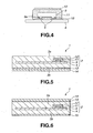
- the IC chip 9 adhered to the insulating substrate 4 is sealed by a sealing material 11 flowed so as to cover the periphery of the IC chip 9, as shown in FIG. 4 , in order to guarantee the conductive characteristic, and is reinforced and protected by a reinforcement material 12 provided on the sealing material 11.
- Epoxy-based, silicon-based, or phenol-based thermosetting resin can be used as the sealing material 11.
- a filler, hollow grains, or foil singly or a complex thereof is mixed into this resin and put to use.
- these materials are used with their size, grading, and mixing ratio thereof adjusted properly.
- Used as the reinforcement material 12 is a substantially circular disk having a larger diameter than the longest dimension value of the IC chip 9.
- the IC chip 9 adhered to the insulating substrate 4 forms a convex part on the insulating substrate 4.
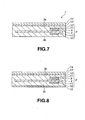
- a convex part is also formed on the surface of the reinforcement material 12 so as to reflect the convex shape of this IC chip 9, so convexes and concaves appear when the reinforcement material 12 is viewed entirely.
- the convexes and concaves of this reinforcement material 12 appear also as convexes and concaves on the card surface. If there are convexes and concaves on the card surface, not only the appearance of the card is degraded but also print characteristics are degraded, e.g., blurring or print errors occur in printing on a visible recording layer.
- the surface variation amount (height difference between convexes and concaves) of this reinforcement material 12 is defined to be 20 ⁇ m or less.
- the surface variation amount (height difference between convexes and concaves) of the reinforcement material 12 is defined to 20 ⁇ m or less, convexes and concaves appearing on the card surface are reduced to provide the card with good appearance.
- excellent print characteristics without blurs or print errors can be attained in printing onto the visible recording layer.
- the surface variation amount of the reinforcement material 12 it is effective to use a material which has Vickers hardness within a range of 200 or more and 580 or less, as the material forming the reinforcement material 12.
- the Vickers hardness is obtained by a measurement method according to JIS-Z2244, and a Vickers hardness tester according to the standard of JIS-B7725 is used.
- the Vickers hardness is less than 200, the shape of the IC chip 9 is reflected on the surface of the reinforcement material 12, or deformation is caused in accordance with contraction/hardening of the sealing material 11. Therefore, the surface variation amount of the reinforcement material 12 cannot be reduced to 20 ⁇ m or less. In addition, the convexes and concaves also appear on the card surface, thereby degrading the appearance and causing blurs and print errors. Thus, print characteristics deteriorate. Meanwhile, if the Vickers hardness is 580 or more, the shape of the IC chip 9 is not reflected on the surface of the reinforcement material 12 or deformation is not caused in accordance with contraction/hardening of the sealing material 11. The surface variation amount of the reinforcement material 12 can be restricted to be very small. However, the reinforcement material 12 is not soft, and therefore, the bending strength is so low that the card cannot be provided with softness.
- the shape of the IC chip 9 can be prevented from being reflected on the surface of the reinforcement material 12, and the surface variation amount of the reinforcement material 12 can be adjusted to 20 ⁇ m or less. Meanwhile, the card can be provided with proper softness.
- the material which has Vickers hardness of 200 or more and less than 580 will be nonferrous metal material such as Cu-Sn-P, Ni-Cu-Zn, Cu-Be-Ni-Co-Fe, or the like, nickel/alloy-based material such as Ni-Co, Ni-Cr, Ni-Mo-Cu, or the like, nickel/ferrous-alloy-based material such as Ni-Fe or the like, titanium/molybdenum/stainless-based material such as SUS304, SUS301, SUS316, SUS631, ASL350, SUS430, SUS420, or the like, or carbon steel such as SK steel, or the like. It is possible to use any of these materials after further increasing the hardness via a heat treatment.
- the thickness of the reinforcement material 12 should preferably be within a range of 50 ⁇ m or more and 100 ⁇ m or less, if the Vickers hardness of the material to be used is 200 or more. If the thickness of the reinforcement material 12 is 50 ⁇ m or less, the convex shape of the IC chip 9 cannot be absorbed, and deformation is caused in accordance with contraction/hardening of the sealing material 11. Thus, the surface variation amount of the reinforcement material 12 cannot be reduced to 20 ⁇ m or less. Alternatively, if the thickness of the reinforcement material 12 exceeds 100 ⁇ m, it is difficult to set the thickness of the IC card 1 within the range according to ISO definitions.
- the thickness of the reinforcement material 12 within a range of 50 to 100 ⁇ m, the convex shape of the IC chip 9 can be absorbed, and deformation in accordance with the contraction/hardening of the sealing material 11 is not caused.
- the surface variation amount of the reinforcement material 12 can be reduced to 20 ⁇ m or less, and the thickness of the IC card 1 can be easily set within the range according to ISO definitions.
- the thickness of the reinforcement material 12 should preferably be within a range of 30 ⁇ m or more and 100 ⁇ m or less. If the thickness of the reinforcement material 12 is 30 ⁇ m or less, the convex shape of the IC chip 9 cannot be absorbed, and deformation is caused in accordance with contraction/hardening of the sealing material 11. Thus, the surface variation amount of the reinforcement material 12 cannot be reduced to 20 ⁇ m or less. In addition, if the thickness of the reinforcement material 12 exceeds 100 ⁇ m, it is difficult to set the thickness of the IC card 1 within a range according to ISO definitions.
- the thickness of the reinforcement material 12 within a range of 30 ⁇ m or more and 100 ⁇ m or less, the convex shape of the IC chip 9 is absorbed and deformation is not caused in accordance with contraction/hardening of the sealing material 11, if the Vickers hardness of the material used for the reinforcement material 12 is 300 or more.
- the surface variation amount of the reinforcement material 12 can be reduced to 20 ⁇ m or less, and the thickness of the IC card 1 is set within a range according to ISO definitions.
- thermoplastic resin sheets 3a and 3b which sandwich the IC module 2 as described above.
- thermoplastic resin having a low-crystallization characteristic of a crystallization rate of 5 % or less it is possible to use copolymer of terephtalic-acid-cyclohexanedimethanol-ethyleneglycol, or alloy ofthis copolymer and polycarbonate, copolymer of terephtalic-acid-isophtalic-acid-ethyleneglycol, or one kind or mixed plural kinds of non-crystal resin selected from a group of resin of copolymer of acrylnitrile-butadiene-styrene, polystyrene resin, polyacrylnitrile resin, polyvinyl-alcohol resin, methyl-polyacrylate resin, polymethyl-methacrylate resin, vinyl acetate resin, poly
- non-crystal resin of these kinds it is possible to use a double-side non-crystal sheet created from non-crystal resin and crystal resin by a co-extrusion method.
- low-crystallization polyester resin of these kinds or other resin may be added with various additives or a substance such as polymer or the like within a range of weight ratio of 50 % or less, or more preferably within 15 % or less.
- a reversible heat-sensitive recording sheet 14 is adhered to one of the surfaces of the thermoplastic resin sheets 3a and 3b by way of an adhesive layer 13 .
- This reversible heat-sensitive recording sheet 14 is constructed by a high-molecule film, a coloring layer, a reversible heat-sensitive recording layer, and a transparent protect layer.
- the high-molecule film it is possible to use various high-molecule films including, for example, a polyethylene-terephtalate (PET) film and the like.
- PET polyethylene-terephtalate
- the coloring layer is prepared, for example, by forming a metal film of aluminum or the like on the high-molecule film by a vacuum deposition method or the like.
- the heat-sensitive recording layer can be selected and used from a high-molecule/low-molecule type in which nebular and transparent states change reversibly in accordance with the change of the crystal state of the organic low-molecule material dispersed in the mother material (matrix) of the resin, and a leuco compound type as a thermo-coloring compound which utilizes reversible coloring reaction between an electron donor type coloring compound and an electron acceptor type compound which are dispersed in the mother material of the resin.
- the heat-sensitive recording layer is formed to have a film thickness of about 4 to 20 ⁇ m by a coating method or the like.
- the organic low-molecule material to be dispersed in the heat-sensitive recording layer will be fatty acid or a derivative of fatty acid or alicyclic organic acid.
- the material will be saturated or non-saturated mono- or di-carboxylic acid, myristic acid, penta-decane acid, palmitic acid, hepta-decane acid, stearic acid, nano-decane acid, arachic acid, behenic acid, lignoceric acid, cerotic acid, montan acid, melissic acid, or the like.
- non-saturated fatty acid will be olein acid, elaidic acid, linoleic acid, sorbic acid, stearol acid, and the like.
- fatty acid, derivative of fatty acid, and alicyclic organic acid are not limited to those described above, and one or two or more kinds of them can be mixed and applied .
- the mother material of the resin will be a single, mixture, or copolymer selected from acryl-based resin, urethane-based resin, polyester-based resin, cellulous-acetate-based resin, nitro-cellulous-based resin, vinyl-chloride-based resin, and vinyl-acetate-based resin. Meanwhile, to control the transparence temperature range of the reversible heat-sensitive recording part, a plasticizer of resin, a high-boiling-point solvent, and the like can be added to the mother material of resin, at 0.1 to 20 weight%.
- a hardener, crosslinking agent, and the like which achieves three-dimensional bridging corresponding to the mother material of resin can be added to the mother material of resin, at 0.5 to 10 weight%.
- the heat-sensitive recording layer of the leuco compound type is a thermo-coloring compound utilizing reversible coloring reaction of a leuco compound and a coloring/decoloring agent which are dispersed in the mother material (matrix) of resin, and can be provided with a film thickness of 4 to 20 ⁇ m by a printing method, coating method, or the like.
- the leuco compound, which is used in the heat-sensitive recording layer and is normally colorless or light-colored will be generally represented by those used for a pressure-sensitive recording paper, heat-sensitive recording paper, light-sensitive recording paper, conductive heat-sensitive recording paper, heat-sensitive transfer paper, and the like.
- Xanthene-based, spiro-pyran-based, lactone-based, fluorane-based, or salton-based compound which has a partial skeleton of lactone, salton, spyro-pyran, or the like is used. However, it is not limited particularly.
- the coloring/decoloring agent is a compound which releases reversibly proton by action of thermal energy and makes both of coloring effect and decoloring effect on the leuco compound. That is, this compound has both of an acidic group consisting of a phenol hydroxyl group or a carboxyl group and a basic group consisting of an amino group, and becomes acidic or basic to color or decolor the leuco compound.
- the basic group may exist as a functional group or as a part of a compound.
- the coloring/decoloring agent having either an acidic or basic group will be, for example, aminobenzoic acid, 0-aminobenzoic acid, 4-amino-3-methylbenzoic acid, 3-amino-4-methylbenzoic acid, 2-amino-5-ethylbenzoic acid, 3-amino-4-buthylbenzoic acid, 4-amino-3-methoxybenzoic acid, 3-amino-4-ethoxybenzoic acid, 2-amino-5-chlorobenzoic acid, 4-amino-3-bromobenzoic acid, 2-amino-2-nitrobenzoic acid, 4-amino-3-nitrobenzoic acid, 3-amino-4-nitrilbenzoic acid, aminosalicylate, diaminobenzoic acid, 2-methyl-5-aminonaphthoic acid, 3-ethyl-4-aminonaphthoic acid, nicotinic acid, isonicotinic acid, 2-methyl
- the compound which includes a basic group as a part of a chloric compound will be a salt or a complex salt of a compound including a phenolic hydroxyl group or a carboxyl group, and a compound including an amino group.
- An example thereof will be a salt or a complex salt of an acid selected from hydroxybenzoic acids, hydroxysalicylic acids, gallic acids, bisphenol acetates, and the like, and a base selected from aliphatic amines, phenylalkylamines, triallylalkylamines, and the like.
- p-hydroxybenzoic acid-alkylamine salt p-hydroxybenzoic acid-phenylalkylamine salt, m-hydroxybenzoic acid-alkylamine salt, p-hydroxybenzoic methyl-alkylamine salt, p-hydroxybenzoic stearyl -alkylamine salt, bisphenol acetate-alkylamine, bisphenol octyl acetate-alkylamine salt, and the like, which are used singly or mixedly.
- the leuco compound and the coloring/decoloring agent are not limited to those described above, and one or two or more kinds of those compounds may be mixed and applied.
- the mother material of resin to be used is a single, mixture, or copolymer of resin selected from acryl-based resin, polyester-based resin, polyurethane-based resin, polyurea, melamine, polycarbonate, polyamido, polyvinylpyrolidone, polyvinylalcohol, polyvinyl chloride, polyvinyl buthylal, and the like.
- a hardener or bridging agent which forms a three-dimensional bridge corresponding to the mother material of resin, can be added to the mother material of resin, 0.5 to 10 weight%.
- an ultraviolet absorbent which has a relatively high compatibility with the leuco compound.
- the surface variation amount (height difference between convexes and concaves) of the reinforcement material 12 of the IC module 2 is defined to be 20 ⁇ m or less, so that convexes and concaves appearing on the card surface can disappear.
- this IC card 1 has a good appearance and provides excellent print characteristics without blurs or print errors, in printing on the visible recording layer.
- this IC card 1 it is possible to use a melt lamination method by heat press.
- the melt lamination method respective materials of the card are sandwiched between mirror plates which are one size larger than the materials, and they are integrated by heat melting press.
- the mirror plates used at thi s time are copper plates subjected to chrome plating, stainless plates whose surfaces are polished, aluminum plates whose surfaces are polished, or the like.
- transparent protect sheets are layered on both surfaces of the printed thermoplastic resin sheets 3a and 3b. At this time, the types of the protect sheets may be different from each other.
- thermoplastic resin sheets 3a and 3b texts or figures can be printed in the same method as conventional printing on papers and plastics, i.e., known printing methods such as a offset printing method, screen printing method, gravure printing method, and the like.
- each material of the integrated card is peeled from the mirror plates, and punching is performed into the card shape with a single blade or a male-female mold.
- the IC card 1 according to the present invention is not limited to the above embodiment but can be variously modified without deviating from the scope of the present invention.
- the embodiment described above has been explained with reference to a case where the reversible heat-sensitive recording sheet 14 is adhered to the thermoplastic resin sheet 3a in the side of the IC-chip-mounting surface.
- the reversible heat-sensitive recording sheet 14 may be adhered to the thermoplastic resin sheet 3b in the side opposite to the side where the IC chip 9 is mounted.
- the reinforcement material 12 may be provided not only on the IC-chip-mounting surface of the IC module 2 but also in the side opposite to the IC-chip mounting surface.
- the static load strength can be increased more.
- the surface of the IC module 2 where the IC chip is not mounted may be sealed with resin, and the reinforcement material 12 may also be provided on the resin.
- the reinforcement material 12 may also be provided on the resin.
- FIG. 9 only the reinforcement material 12 may be provided. Note that FIG.
- the IC card 1 shows an example of the IC card 1 in which the reinforcement material 12 is provided on the surface of the IC module 2 where the IC chip is not mounted, and further, the protect layer 15 is provided on the thermoplastic resin sheet 3b in the side opposite to the thermoplastic resin sheet 3a to which the reversible heat-sensitive recording sheet 14 is adhered.
- the IC module 2 is constructed in a structure in which only the IC-chip mounting part of the insulating substrate 4 is made of a glass epoxy substrate, a plastic substrate, or the like, and the part of the antenna coil 5 is jointed optionally and electrically by a connection lead 16.
- an antenna module was prepared.
- An IC chip (4 mm ⁇ 4mm ⁇ 180 ⁇ m) was mounted on the antenna module with a flip-chip adhesive organic conductive film having a thickness of 30 ⁇ m inserted therebetween.
- an epoxy-based sealing material and further A5052 (having a diameter of 7 mm and thickness of 100 ⁇ m) as an IC chip reinforcement material were provided and hardened at 110°C to prepare an IC module.
- thermoplastic resin sheet was prepared as follows. Terephthalic acid, copolymer (PET-G) of cyclohexane dimethanol and ethylene glycol, titanium oxide as a white color filler were mixed at a weight ratio of 10 %, and were sheeted to have a thickness of 350 ⁇ m by a melt-extrusion method, to obtain a thermoplastic resin sheet made of white PET-G.
- PET-G Terephthalic acid, copolymer of cyclohexane dimethanol and ethylene glycol, titanium oxide as a white color filler
- thermoplastic resin sheet was printed on one surface of this thermoplastic resin sheet by the screen printing method and the offset printing method.
- a set of the printed thermoplastic resin sheets for the front and back sides were prepared and arranged to sandwich the IC module prepared beforehand, with their printed surfaces oriented outsides. Four corners of the sheets are welded and fixed temporarily by an ultrasonic welding device.
- a orientative polypropulene film sheet (OPP) having a thickness of 60 ⁇ m was provided outside the temporarily fixed sheet, and stainless mirror plates having a thickness of 3 mm were further arranged to sandwich them from outside. They were pressed into contact and thermally melted under conditions of a temperature of 170 °C and a pressure of 15 kg/cm 2 by heat-melting press, and were further cooled and solidified.
- OPP was peeled to obtain a card-forming member which contains an IC module inlet.
- a reversible heat-sensitive recording sheet was prepared as follows. At first, an Al layer was formed with a thickness of about 50 ⁇ , as a coloring layer, on a polyethylene terephthalate film having a thickness of 50 ⁇ m by a vacuum vaporization method. A heat-sensitive recording layer coating material made of organic molecules dispersed in resin was coated thereon with a coating thickness of 10 ⁇ m at a dry temperature of 120°C with use of a gravure method. Further, a protection layer was coated thereon with a coating thickness of 3 ⁇ m by a gravure printing method. Next, an adhesive coating material was coated with a thickness of 3 ⁇ m on the back surface of this sheet, at a dry temperature of 100°C , by the gravure method. A reversible heat-sensitive recording sheet was thus obtained.
- compositions of the heat-sensitive recording coating material, protection layer coating material, and adhesive coating material used were as follows.
- the card-forming member including the IC module, and the reversible heat-sensitive recording sheet were temporarily fixed again by the ultrasonic welding machine, with the heat-sensitive recording layer situated outsides.
- Orientative polypropylene film sheet was provided outside the temporarily fixed sheet, and further, stainless mirror plates having a thickness of 3 mm were used to sandwich them from outside. They were pressed and thermally melted under conditions of a temperature of 120°C and a pressure of 15 kg/cm 2 , and were cooled and solidified. Thereafter, punching was carried out into a card shape. In the manner as described above, a non-contact card having a reversible heat-sensitive recording layer was prepared.
- Non-contact IC cards were prepared in the same manner as the sample 1 except that the materials shown in Table 1 were used as materials of the reinforcement material or the thermoplastic resin sheet.
- Non-contact IC cards were prepared in the same manner as the sample 1 except that the materials shown in Table 1 were used as materials of the reinforcement material or the thermoplastic resin sheet and that a sealing material and a reinforcement material were further provided on the back surface side of the IC module which was opposite to the IC-mounting surface.
- Non-contact IC cards were prepared in the same manner as the sample 1 except that the materials shown in Table 1 were used as materials of the reinforcement material or the thermoplastic resin sheet, that a sealing material and a reinforcement material were further provided on the back surface side of the IC module which is opposite to the IC-mounting surface, and a reversible heat-sensitive recording layer was provided on the side of the surface where no IC was mounted.
- thermoplastic resin sheets made of white PET-G sheets was set to 330 ⁇ m.
- the IC module was sandwiched between the back PET-G sheet where figures were printed like the sample 1 and the front PET-G sheet without figures, and was temporarily fixed therebetween.
- Card-forming members including IC modules were prepared in the same manner as the sample 1 except that a transparent PET-G sheet having a thickness of 50 ⁇ m and added with no white filler was provided on the figured surface of the temporarily fixed card-forming member.
- Non-contact IC cards each having a reversible heat-sensitive recording layer were thus prepared.
- Non-contact IC cards were prepared in the same manner as the sample 1 except that the materials shown in Table 1 were used as materials of the reinforcement material or the thermoplastic resin sheet and that the reversible heat-sensitive recording layer was set in the surface where no IC was mounted.
- the print characteristic a heat-sensitive printer manufactured by Matsushita Electric Industrial Co., Ltd. was used, and printing was carried out where application energy of the thermal head was 0.5 mJ/dot. The printed surface of the card was observed with eyes. When a print omission is caused at the part where the IC-mounting part was reinforced by the reinforcement material, the print characteristic was evaluated as ⁇ . Otherwise, when there was no print omission, the print characteristic was evaluated as o.
- print layer adhesion With respect to the print layer adhesion, printing and erasure were repeated 500 times. The condition of a figure on the print layer on the back surface of the heat-sensitive recording layer was observed with eyes. When a defect or peeling appears on the figure, the print layer adhesion was evaluated as ⁇ . Otherwise, when there was no defect or peeling, the print layer adhesion was evaluated as o.
- the load position was at the center of the IC-chip mounting part, and the top end shape of the probe was set to be a sphere having a radius of 0.2 mm.
- the load test speed was set to 0.5 mm/min.
- a breakdown was decided at the time when communication became impossible.
- the bending test was carried out according to the method described in JIS-X-6305. IC operation checks before and after the bending test were made with use of a reader/writer (communication device) manufactured by SONY (where 20 ICs were checked).
- the possibility of Cl-containing-gas generation was evaluated to be present if there is a possibility of generating a gas containing Cl when a card is subjected to incineration deposition as abandonment processing. Otherwise, if there is no possibility of generating a Cl gas, the possibility of Cl-containing-gas generation was evaluated to be absent.
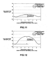
- FIG. 11 shows the surface shape measurement results of the reinforcement material with respect to the IC module of the sample 7.
- FIG. 12 shows the surface shape measurement results of the reinforcement material with respect to the IC module of the sample 1.
- the shape of the IC chip is prevented from being reflected on the surface of the reinforcement material and deformation is prevented from being caused in accordance with contraction/hardening of the sealing material, so that the surface shift among of the reinforcement material can be adjusted to 20 ⁇ m or less.
- the card is provided with optimal softness, so that the reliability in IC operation in the bending test can be improved excellently.
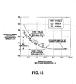
- FIG. 13 shows the relationship between the Vickers hardness and thickness of the reinforcement material for every thickness of the reinforcement material.
- the reinforcement material had poor elasticity and causes deformation of the shape in accordance with hardening/contraction of the sealing material, so it is difficult to ensure reliability of the IC operation. Meanwhile, in the range that the Vickers hardness is 580 or more or the thickness exceeds 100 ⁇ m, the reinforcement material becomes fragile when the hardness exceeds. In the range in which the thickness exceeds, only the reinforcement material part becomes easily thick and becomes difficult to set it within the definitions according to JIS.
- the reliability of the mechanical strength of the IC chip part increases by providing the IC module with reinforcement material having Vickers hardness within a range of 300 or more and less than 580 and a thickness within a range of 30 ⁇ m or more and 100 ⁇ m or less, and by setting the difference of elevation of the surface shape within 20 ⁇ m.
- reinforcement material having Vickers hardness within a range of 300 or more and less than 580 and a thickness within a range of 30 ⁇ m or more and 100 ⁇ m or less
- the reinforcement material had poor elasticity and causes deformation of the shape in accordance with hardening/contraction of the sealing material, so it is difficult to ensure reliability of the IC operation. Meanwhile, in the range that the Vickers hardness is 580 or more or the thickness exceeds 100 ⁇ m, the reinforcement material becomes fragile when the hardness exceeds. In the range in which the thickness exceeds, only the reinforcement material part becomes easily thick and becomes difficult to set it within the definitions according to JIS.
- the reliability of the mechanical strength of the IC chip part increases by providing the IC module with reinforcement material having Vickers hardness within a range of 200 or more and less than 580 and a thickness within a range of 50 ⁇ m or more and 100 ⁇ m or less, and by setting the difference of elevation of the surface shape within 20 ⁇ m.
- reinforcement material having Vickers hardness within a range of 200 or more and less than 580 and a thickness within a range of 50 ⁇ m or more and 100 ⁇ m or less, and by setting the difference of elevation of the surface shape within 20 ⁇ m.
- thermoplastic resin sheets In the samples 19 and 20, polyvinyl chloride (PVC) was used for thermoplastic resin sheets, there is a possibility of generating a gas which may cause problems of hydrogen chloride, dioxin, and the like in incineration processing. In other samples which used material containing no chloride for the thermoplastic resin sheets, there is little possibility of generating a gas which may cause problems of hydrogen chloride, dioxin, and the like in incineration processing. Accordingly, it has been found that the problems of hydrogen chloride, dioxin, and the like can be avoided in incineration processing by using material containing no chloride for the thermoplastic resin sheets.
- the static load strength can be further increased by providing the reinforcement material not only on the IC chip mounting surface but also on the surface where no IC chip was mounted, from comparison between the samples 5, 8, and 11, in which the reinforcement material was provided only on the IC chip mounting surface of the IC module, and the samples 21 to 23, in which the same reinforcement material was provided in the side of the IC module opposite to the IC-chip mounting surface.
- the reinforcement material was provided on both of the IC chip mounting surface and the surface where no IC was mounted, and further, the heat-sensitive recording layer is provided not in the side of the IC-mounting surface but on the surface where no IC was mounted. From these samples 24 to 28, it has been found that reliability of the mechanical strength of the IC part increased except the sample 24 in which the difference between the concaves and convexes exceeded 20 ⁇ m, and that a non-contact card which had satisfactory print characteristic could be obtained by further providing the heat-sensitive recording layer in the side of the surface where no IC was mounted.
- the static load strength can be increased and the printed surface can be protected by providing the reinforcement material also on the surface where no IC chip was mounted, from comparison between the samples 29 to 31, in which the reinforcement material was provided only on the IC chip mounting surface, and the samples 32 to 34, in which the reinforcement material was provided also on the surface where no reinforcement material was provided.
- concaves and convexes disappear from the card surface, by defining the surface variation amount (difference between convexes and concaves) of reinforcement material provided on the IC module, to be 20 ⁇ m or less.
- the card has a good appearance and provides excellent print characteristic without blurs or print omissions even in printing on a visible recording layer.
Landscapes
- Engineering & Computer Science (AREA)
- Computer Hardware Design (AREA)
- Microelectronics & Electronic Packaging (AREA)
- Physics & Mathematics (AREA)
- General Physics & Mathematics (AREA)
- Theoretical Computer Science (AREA)
- Credit Cards Or The Like (AREA)
Applications Claiming Priority (3)
| Application Number | Priority Date | Filing Date | Title |
|---|---|---|---|
| JP2000365967 | 2000-11-30 | ||
| JP2000365967A JP4873776B2 (ja) | 2000-11-30 | 2000-11-30 | 非接触icカード |
| PCT/JP2001/010246 WO2002043967A1 (fr) | 2000-11-30 | 2001-11-22 | Carte a circuit integre sans contact |
Publications (3)
| Publication Number | Publication Date |
|---|---|
| EP1243442A1 EP1243442A1 (en) | 2002-09-25 |
| EP1243442A4 EP1243442A4 (en) | 2006-03-29 |
| EP1243442B1 true EP1243442B1 (en) | 2015-11-11 |
Family
ID=18836652
Family Applications (1)
| Application Number | Title | Priority Date | Filing Date |
|---|---|---|---|
| EP01998452.5A Expired - Lifetime EP1243442B1 (en) | 2000-11-30 | 2001-11-22 | Noncontact ic card |
Country Status (7)
Families Citing this family (67)
| Publication number | Priority date | Publication date | Assignee | Title |
|---|---|---|---|---|
| US6615189B1 (en) | 1998-06-22 | 2003-09-02 | Bank One, Delaware, National Association | Debit purchasing of stored value card for use by and/or delivery to others |
| US7809642B1 (en) | 1998-06-22 | 2010-10-05 | Jpmorgan Chase Bank, N.A. | Debit purchasing of stored value card for use by and/or delivery to others |
| US8793160B2 (en) | 1999-12-07 | 2014-07-29 | Steve Sorem | System and method for processing transactions |
| WO2003010701A1 (en) | 2001-07-24 | 2003-02-06 | First Usa Bank, N.A. | Multiple account card and transaction routing |
| US8020754B2 (en) | 2001-08-13 | 2011-09-20 | Jpmorgan Chase Bank, N.A. | System and method for funding a collective account by use of an electronic tag |
| US7899753B1 (en) | 2002-03-25 | 2011-03-01 | Jpmorgan Chase Bank, N.A | Systems and methods for time variable financial authentication |
| WO2003083619A2 (en) | 2002-03-29 | 2003-10-09 | Bank One, Delaware, N.A. | System and process for performing purchase transaction using tokens |
| KR100467634B1 (ko) * | 2002-07-16 | 2005-01-24 | 삼성에스디에스 주식회사 | 스마트 카드 및 그의 제조방법 |
| US6726099B2 (en) * | 2002-09-05 | 2004-04-27 | Honeywell International Inc. | RFID tag having multiple transceivers |
| US7809595B2 (en) | 2002-09-17 | 2010-10-05 | Jpmorgan Chase Bank, Na | System and method for managing risks associated with outside service providers |
| US20040122736A1 (en) | 2002-10-11 | 2004-06-24 | Bank One, Delaware, N.A. | System and method for granting promotional rewards to credit account holders |
| FI20022070A7 (fi) * | 2002-11-20 | 2004-05-21 | Rafsec Oy | Transponderi |
| JP2004185208A (ja) * | 2002-12-02 | 2004-07-02 | Sony Corp | Icカード |
| US7588184B2 (en) | 2003-01-03 | 2009-09-15 | American Express Travel Related Services Company, Inc. | Metal-containing transaction card and method of making the same |
| US7823777B2 (en) * | 2003-01-03 | 2010-11-02 | American Express Travel Related Services Company, Inc. | Metal-containing transaction card and method of making same |
| US8033457B2 (en) | 2003-01-03 | 2011-10-11 | American Express Travel Related Services Company, Inc. | Metal-containing transaction card and method of making the same |
| AU2003300451B2 (en) | 2003-01-03 | 2009-12-17 | American Express Travel Related Services Company, Inc. | Metal containing transaction card and method of making the same |
| FR2853115B1 (fr) * | 2003-03-28 | 2005-05-06 | A S K | Procede de fabrication d'antenne de carte a puce sur un support thermoplastique et carte a puce obtenue par ledit procede |
| JP2004348590A (ja) * | 2003-05-23 | 2004-12-09 | Konica Minolta Photo Imaging Inc | Icカード及びicカード製造方法 |
| US8306907B2 (en) | 2003-05-30 | 2012-11-06 | Jpmorgan Chase Bank N.A. | System and method for offering risk-based interest rates in a credit instrument |
| JP2005014302A (ja) * | 2003-06-24 | 2005-01-20 | Sony Corp | 合成樹脂カード及びその製造方法 |
| US7237719B2 (en) * | 2003-09-03 | 2007-07-03 | Stmicroelectronics, Inc. | Method and apparatus for a USB and contactless smart card device |
| JP3803097B2 (ja) | 2003-10-07 | 2006-08-02 | 株式会社日立製作所 | 無線通信媒体の製造方法 |
| JP4504693B2 (ja) * | 2004-01-30 | 2010-07-14 | トッパン・フォームズ株式会社 | スレッド、icチップ入りシート及びその製造方法 |
| JP2005234683A (ja) * | 2004-02-17 | 2005-09-02 | Matsushita Electric Ind Co Ltd | Icカード |
| US7154170B2 (en) * | 2004-03-31 | 2006-12-26 | Intel Corporation | Semiconductor package security features using thermochromatic inks and three-dimensional identification coding |
| KR100602621B1 (ko) * | 2004-06-16 | 2006-07-19 | 한국조폐공사 | 조립식 콤비카드 및 이의 제조방법 |
| JP2006024087A (ja) * | 2004-07-09 | 2006-01-26 | Nec Corp | 無線デバイス、その製造方法、その検査方法及び検査装置並びに無線装置及びその製造方法 |
| US7501381B2 (en) * | 2004-09-14 | 2009-03-10 | Ricoh Company, Ltd. | Reversible thermosensitive recording medium, image processing method, and image processing apparatus |
| US7401731B1 (en) | 2005-05-27 | 2008-07-22 | Jpmorgan Chase Bank, Na | Method and system for implementing a card product with multiple customized relationships |
| JP4815891B2 (ja) * | 2005-06-22 | 2011-11-16 | 株式会社日立製作所 | 無線icタグ及びアンテナの製造方法 |
| TWI339358B (en) * | 2005-07-04 | 2011-03-21 | Hitachi Ltd | Rfid tag and manufacturing method thereof |
| EP1780662A1 (fr) * | 2005-10-27 | 2007-05-02 | Axalto SA | Module renforcé pour carte à puce et procédé de fabrication dudit module |
| US7595732B2 (en) * | 2006-03-31 | 2009-09-29 | Broadcom Corporation | Power generating circuit |
| JP2007261121A (ja) | 2006-03-29 | 2007-10-11 | Ricoh Co Ltd | 可逆性感熱記録媒体用洗浄方法 |
| US20070290048A1 (en) * | 2006-06-20 | 2007-12-20 | Innovatier, Inc. | Embedded electronic device and method for manufacturing an embedded electronic device |
| TWI506560B (zh) * | 2006-08-07 | 2015-11-01 | Kuo Ching Chiang | Non - contact credit card and financial card trading device and its non - contact transaction method |
| TWI584199B (zh) * | 2006-08-07 | 2017-05-21 | 江國慶 | 具有非接觸式儲值卡之手持通訊裝置及其方法 |
| JP4382783B2 (ja) * | 2006-08-09 | 2009-12-16 | 富士通株式会社 | Rfidタグ |
| JP2009178843A (ja) | 2006-08-22 | 2009-08-13 | Rynne Group Llc | 識別カードおよびその識別カードを使用した識別カード取引システム |
| JP4860436B2 (ja) * | 2006-11-07 | 2012-01-25 | トッパン・フォームズ株式会社 | Icカードおよびその製造方法 |
| WO2008056714A1 (fr) * | 2006-11-07 | 2008-05-15 | Toppan Forms Co., Ltd. | Matériau de base de fenêtre, et carte à module incorporé et son procédé de fabrication |
| JP2008210032A (ja) * | 2007-02-23 | 2008-09-11 | Fujitsu Ltd | Rfidタグ |
| JP2008204139A (ja) * | 2007-02-20 | 2008-09-04 | Toppan Forms Co Ltd | 非接触型データ受送信体 |
| JP5145881B2 (ja) | 2007-11-07 | 2013-02-20 | 富士通株式会社 | Rfidタグ |
| USD636021S1 (en) | 2008-07-17 | 2011-04-12 | Jpmorgan Chase Bank, N.A. | Eco-friendly transaction device |
| USD617378S1 (en) | 2009-02-12 | 2010-06-08 | Jpmorgan Chase Bank, N.A. | Transaction device with a gem-like surface appearance |
| USD620975S1 (en) | 2009-02-12 | 2010-08-03 | Jpmorgan Chase Bank, N.A. | Transaction device |
| US8725589B1 (en) | 2009-07-30 | 2014-05-13 | Jpmorgan Chase Bank, N.A. | Methods for personalizing multi-layer transaction cards |
| USD623690S1 (en) | 2010-03-05 | 2010-09-14 | Jpmorgan Chase Bank, N.A. | Metal transaction device with gem-like surface |
| AU2011224861B2 (en) * | 2010-03-08 | 2015-11-26 | Sensormatic Electronics Llc | System and method for security tag deployment using reversible adhesives |
| USD643064S1 (en) | 2010-07-29 | 2011-08-09 | Jpmorgan Chase Bank, N.A. | Metal transaction device with gem-like surface |
| KR101275983B1 (ko) * | 2010-09-01 | 2013-06-14 | 현대카드 주식회사 | 메탈 결제카드 및 그 제작 방법 |
| US10032099B2 (en) | 2012-07-20 | 2018-07-24 | CPI Card Group—Colorado, Inc. | Weighted transaction card |
| US8857722B2 (en) | 2012-07-20 | 2014-10-14 | CPI Card Group—Colorado, Inc. | Weighted transaction card |
| CN103996351B (zh) * | 2013-02-20 | 2020-01-21 | 泰科消防及安全有限公司 | 粘合剂结合的物品保护标签 |
| USD854083S1 (en) | 2013-03-27 | 2019-07-16 | Jpmorgan Chase Bank, N.A. | Hybrid transaction device |
| DE102013109976B4 (de) * | 2013-09-11 | 2017-06-22 | Infineon Technologies Ag | Chipkartenmodul-Anordnung, Chipkarte, Verfahren zum Herstellen einer Chipkartenmodul-Anordnung und Verfahren zum Herstellen einer Chipkarte |
| US9442662B2 (en) * | 2013-10-18 | 2016-09-13 | Sandisk Technologies Llc | Device and method for managing die groups |
| WO2015061611A1 (en) | 2013-10-25 | 2015-04-30 | Cpi Card Group - Colorado, Inc. | Multi-metal layered card |
| JP6353763B2 (ja) * | 2014-09-30 | 2018-07-04 | 新光電気工業株式会社 | 半導体装置及びその製造方法 |
| JP6280014B2 (ja) * | 2014-09-30 | 2018-02-14 | 新光電気工業株式会社 | 半導体装置及びその製造方法 |
| US20160232438A1 (en) | 2015-02-06 | 2016-08-11 | American Express Travel Related Services Company, Inc. | Ceramic-containing transaction cards |
| WO2017210305A1 (en) | 2016-06-01 | 2017-12-07 | Cpi Card Group - Colorado, Inc. | Ic chip card with integrated biometric sensor pads |
| EP3582973B1 (en) | 2017-02-14 | 2023-06-28 | CPI Card Group - Colorado, Inc. | Edge-to-edge metal card and production method |
| KR102242063B1 (ko) | 2019-11-04 | 2021-05-12 | (주)비티비엘 | 품질이 우수한 휴대용 카드 |
| JP6871464B1 (ja) * | 2020-08-18 | 2021-05-12 | 三菱瓦斯化学株式会社 | 樹脂組成物、樹脂シート、多層体、および、カード |
Family Cites Families (19)
| Publication number | Priority date | Publication date | Assignee | Title |
|---|---|---|---|---|
| JPS61123990A (ja) * | 1984-11-05 | 1986-06-11 | Casio Comput Co Ltd | Icカ−ド |
| JPH0823149A (ja) * | 1994-05-06 | 1996-01-23 | Seiko Epson Corp | 半導体装置及びその製造方法 |
| DE4443980C2 (de) * | 1994-12-11 | 1997-07-17 | Angewandte Digital Elektronik | Verfahren zur Herstellung von Chipkarten und Chipkarte hergestellt nach diesem Verfahren |
| CA2192076C (en) * | 1995-04-13 | 2000-01-18 | Masao Gogami | Ic card and ic module |
| JPH09156267A (ja) * | 1995-12-06 | 1997-06-17 | Watada Insatsu Kk | プラスチックカード |
| DE19632813C2 (de) * | 1996-08-14 | 2000-11-02 | Siemens Ag | Verfahren zur Herstellung eines Chipkarten-Moduls, unter Verwendung dieses Verfahrens hergestellter Chipkarten-Modul und diesen Chipkarten-Modul enthaltende Kombi-Chipkarte |
| JPH1076779A (ja) * | 1996-09-04 | 1998-03-24 | Toppan Printing Co Ltd | 可逆性感熱記録カード及びその製造方法 |
| JPH10198950A (ja) * | 1996-11-18 | 1998-07-31 | Dainippon Printing Co Ltd | 磁気カード |
| JPH10203059A (ja) | 1997-01-20 | 1998-08-04 | Toshiba Corp | 無線カード |
| US6607135B1 (en) * | 1997-06-23 | 2003-08-19 | Rohm Co., Ltd. | Module for IC card, IC card, and method for manufacturing module for IC card |
| JP2000090229A (ja) * | 1998-07-13 | 2000-03-31 | Minolta Co Ltd | 情報記録表示カ―ド及びそれを用いた情報記録表示システム |
| JP2000048151A (ja) * | 1998-07-30 | 2000-02-18 | Toppan Printing Co Ltd | 非接触icカード |
| JP2000057295A (ja) * | 1998-08-14 | 2000-02-25 | Hitachi Maxell Ltd | 非接触icカード及びその製造方法 |
| JP3340076B2 (ja) * | 1998-10-16 | 2002-10-28 | スター精密株式会社 | 可視表示カードおよびカード処理システム |
| JP4215886B2 (ja) * | 1999-02-03 | 2009-01-28 | ソニー株式会社 | 半導体集積回路チップの封止方法、半導体集積回路カードの製造方法 |
| JP2000137781A (ja) * | 1998-10-30 | 2000-05-16 | Hitachi Ltd | カード型電子回路基板及びその製造方法 |
| JP4284750B2 (ja) * | 1999-04-26 | 2009-06-24 | 凸版印刷株式会社 | カード及びカードの製造方法 |
| JP4649688B2 (ja) * | 1999-04-28 | 2011-03-16 | 凸版印刷株式会社 | 非接触式icカード |
| JP2001351076A (ja) * | 2000-06-05 | 2001-12-21 | Toppan Printing Co Ltd | 非接触icカード及び補強板搭載方法 |
-
2000
- 2000-11-30 JP JP2000365967A patent/JP4873776B2/ja not_active Expired - Lifetime
-
2001
- 2001-11-22 WO PCT/JP2001/010246 patent/WO2002043967A1/ja active Application Filing
- 2001-11-22 KR KR1020027009761A patent/KR100859105B1/ko not_active Expired - Fee Related
- 2001-11-22 CN CNB018042899A patent/CN1264697C/zh not_active Expired - Fee Related
- 2001-11-22 US US10/182,085 patent/US6942156B2/en not_active Expired - Lifetime
- 2001-11-22 EP EP01998452.5A patent/EP1243442B1/en not_active Expired - Lifetime
- 2001-11-27 TW TW090129290A patent/TW561415B/zh not_active IP Right Cessation
Also Published As
| Publication number | Publication date |
|---|---|
| EP1243442A4 (en) | 2006-03-29 |
| TW561415B (en) | 2003-11-11 |
| JP4873776B2 (ja) | 2012-02-08 |
| US20030062420A1 (en) | 2003-04-03 |
| US6942156B2 (en) | 2005-09-13 |
| KR20020081283A (ko) | 2002-10-26 |
| JP2002170087A (ja) | 2002-06-14 |
| CN1264697C (zh) | 2006-07-19 |
| WO2002043967A1 (fr) | 2002-06-06 |
| EP1243442A1 (en) | 2002-09-25 |
| KR100859105B1 (ko) | 2008-09-18 |
| CN1396869A (zh) | 2003-02-12 |
Similar Documents
| Publication | Publication Date | Title |
|---|---|---|
| EP1243442B1 (en) | Noncontact ic card | |
| EP1394734B1 (en) | Ic card | |
| US7377446B2 (en) | IC card | |
| KR20040004069A (ko) | Ic 카드 | |
| KR20030087936A (ko) | Ic 카드 | |
| JP4278039B2 (ja) | 非接触icカード、インレットシート及び非接触icカードの製造方法 | |
| JP4770049B2 (ja) | 非接触型icカードおよびその製造方法 | |
| JP2008059240A (ja) | インターポーザ保護構造を有するicタグとicタグ付きリライタブルシート | |
| JP2002163624A (ja) | Icカード | |
| JP5136049B2 (ja) | 非接触icカードの製造方法 | |
| JP2004192568A (ja) | Icカード | |
| JP2002163623A (ja) | Icカード | |
| JP2005092488A (ja) | 情報表示手段付icカードおよびその製造方法 | |
| JP2002197433A (ja) | Icカード及びその製造方法 | |
| JPH1035161A (ja) | Icカードおよびicカードの製造方法 | |
| JP2004338310A (ja) | カードの製造方法及びカード | |
| JP2004326351A (ja) | Icカード及びその製造方法 | |
| JPH09315057A (ja) | Icカードおよびicカードの製造方法 | |
| JP2001283172A (ja) | 非接触型icカード | |
| JP2001155126A (ja) | 非接触icカード用ベース基材及びそれを用いた非接触icカード | |
| JP2008040641A (ja) | インターポーザ保護構造を有するicタグとicタグ付きリライタブルシート | |
| HK1069469B (en) | Ic card |
Legal Events
| Date | Code | Title | Description |
|---|---|---|---|
| PUAI | Public reference made under article 153(3) epc to a published international application that has entered the european phase |
Free format text: ORIGINAL CODE: 0009012 |
|
| AK | Designated contracting states |
Kind code of ref document: A1 Designated state(s): AT BE CH CY DE DK ES FI FR GB GR IE IT LI LU MC NL PT SE TR |
|
| 17P | Request for examination filed |
Effective date: 20021107 |
|
| RBV | Designated contracting states (corrected) |
Designated state(s): DE FI FR GB SE |
|
| A4 | Supplementary search report drawn up and despatched |
Effective date: 20060215 |
|
| 17Q | First examination report despatched |
Effective date: 20100602 |
|
| REG | Reference to a national code |
Ref country code: DE Ref legal event code: R079 Ref document number: 60149669 Country of ref document: DE Free format text: PREVIOUS MAIN CLASS: B42D0015100000 Ipc: G06K0019070000 |
|
| GRAP | Despatch of communication of intention to grant a patent |
Free format text: ORIGINAL CODE: EPIDOSNIGR1 |
|
| RIC1 | Information provided on ipc code assigned before grant |
Ipc: G06K 19/07 20060101AFI20150326BHEP Ipc: G06K 19/077 20060101ALI20150326BHEP |
|
| INTG | Intention to grant announced |
Effective date: 20150415 |
|
| GRAS | Grant fee paid |
Free format text: ORIGINAL CODE: EPIDOSNIGR3 |
|
| RAP1 | Party data changed (applicant data changed or rights of an application transferred) |
Owner name: SONY CORPORATION |
|
| RIN1 | Information on inventor provided before grant (corrected) |
Inventor name: MATSUMURA, SHINICHI, SONY CORPORATION Inventor name: YAMAZAKI, NORIHIKO, SONY CORPORATION Inventor name: OHTA, EIJI, SONY CORPORATION |
|
| GRAA | (expected) grant |
Free format text: ORIGINAL CODE: 0009210 |
|
| AK | Designated contracting states |
Kind code of ref document: B1 Designated state(s): DE FI FR GB SE |
|
| REG | Reference to a national code |
Ref country code: GB Ref legal event code: FG4D |
|
| REG | Reference to a national code |
Ref country code: FR Ref legal event code: PLFP Year of fee payment: 15 |
|
| REG | Reference to a national code |
Ref country code: DE Ref legal event code: R096 Ref document number: 60149669 Country of ref document: DE |
|
| PG25 | Lapsed in a contracting state [announced via postgrant information from national office to epo] |
Ref country code: SE Free format text: LAPSE BECAUSE OF FAILURE TO SUBMIT A TRANSLATION OF THE DESCRIPTION OR TO PAY THE FEE WITHIN THE PRESCRIBED TIME-LIMIT Effective date: 20151111 Ref country code: FI Free format text: LAPSE BECAUSE OF FAILURE TO SUBMIT A TRANSLATION OF THE DESCRIPTION OR TO PAY THE FEE WITHIN THE PRESCRIBED TIME-LIMIT Effective date: 20151111 |
|
| REG | Reference to a national code |
Ref country code: DE Ref legal event code: R097 Ref document number: 60149669 Country of ref document: DE |
|
| PLBE | No opposition filed within time limit |
Free format text: ORIGINAL CODE: 0009261 |
|
| STAA | Information on the status of an ep patent application or granted ep patent |
Free format text: STATUS: NO OPPOSITION FILED WITHIN TIME LIMIT |
|
| 26N | No opposition filed |
Effective date: 20160812 |
|
| REG | Reference to a national code |
Ref country code: FR Ref legal event code: PLFP Year of fee payment: 16 |
|
| REG | Reference to a national code |
Ref country code: FR Ref legal event code: PLFP Year of fee payment: 17 |
|
| PGFP | Annual fee paid to national office [announced via postgrant information from national office to epo] |
Ref country code: DE Payment date: 20181120 Year of fee payment: 18 |
|
| PGFP | Annual fee paid to national office [announced via postgrant information from national office to epo] |
Ref country code: GB Payment date: 20181120 Year of fee payment: 18 Ref country code: FR Payment date: 20181121 Year of fee payment: 18 |
|
| REG | Reference to a national code |
Ref country code: DE Ref legal event code: R119 Ref document number: 60149669 Country of ref document: DE |
|
| GBPC | Gb: european patent ceased through non-payment of renewal fee |
Effective date: 20191122 |
|
| PG25 | Lapsed in a contracting state [announced via postgrant information from national office to epo] |
Ref country code: FR Free format text: LAPSE BECAUSE OF NON-PAYMENT OF DUE FEES Effective date: 20191130 Ref country code: GB Free format text: LAPSE BECAUSE OF NON-PAYMENT OF DUE FEES Effective date: 20191122 Ref country code: DE Free format text: LAPSE BECAUSE OF NON-PAYMENT OF DUE FEES Effective date: 20200603 |