EP1193676A2 - Transistor à couche mince pour l'alimentation d'un élément électroluminescent - Google Patents
Transistor à couche mince pour l'alimentation d'un élément électroluminescent Download PDFInfo
- Publication number
- EP1193676A2 EP1193676A2 EP01308326A EP01308326A EP1193676A2 EP 1193676 A2 EP1193676 A2 EP 1193676A2 EP 01308326 A EP01308326 A EP 01308326A EP 01308326 A EP01308326 A EP 01308326A EP 1193676 A2 EP1193676 A2 EP 1193676A2
- Authority
- EP
- European Patent Office
- Prior art keywords
- thin film
- film transistor
- driven
- layer
- tft
- Prior art date
- Legal status (The legal status is an assumption and is not a legal conclusion. Google has not performed a legal analysis and makes no representation as to the accuracy of the status listed.)
- Withdrawn
Links
- 239000010409 thin film Substances 0.000 title claims description 122
- 238000009413 insulation Methods 0.000 claims description 49
- 239000004065 semiconductor Substances 0.000 claims description 35
- 239000011159 matrix material Substances 0.000 claims description 33
- 238000005401 electroluminescence Methods 0.000 claims description 11
- 150000002894 organic compounds Chemical class 0.000 claims description 8
- 238000000137 annealing Methods 0.000 claims description 5
- 238000005224 laser annealing Methods 0.000 abstract description 16
- 239000010410 layer Substances 0.000 description 216
- 238000005286 illumination Methods 0.000 description 45
- 230000015572 biosynthetic process Effects 0.000 description 33
- 239000003990 capacitor Substances 0.000 description 19
- 238000010586 diagram Methods 0.000 description 19
- 239000010408 film Substances 0.000 description 18
- 238000000034 method Methods 0.000 description 11
- 239000000463 material Substances 0.000 description 10
- 229910021420 polycrystalline silicon Inorganic materials 0.000 description 10
- 230000009467 reduction Effects 0.000 description 10
- 239000000758 substrate Substances 0.000 description 9
- 239000011229 interlayer Substances 0.000 description 8
- 229910021417 amorphous silicon Inorganic materials 0.000 description 6
- 229910052751 metal Inorganic materials 0.000 description 6
- 239000002184 metal Substances 0.000 description 6
- 230000000694 effects Effects 0.000 description 5
- 230000005684 electric field Effects 0.000 description 5
- 230000005525 hole transport Effects 0.000 description 5
- 230000008569 process Effects 0.000 description 5
- 238000012935 Averaging Methods 0.000 description 4
- 230000008901 benefit Effects 0.000 description 4
- 229910052782 aluminium Inorganic materials 0.000 description 3
- XAGFODPZIPBFFR-UHFFFAOYSA-N aluminium Chemical compound [Al] XAGFODPZIPBFFR-UHFFFAOYSA-N 0.000 description 3
- 230000000903 blocking effect Effects 0.000 description 3
- VBVAVBCYMYWNOU-UHFFFAOYSA-N coumarin 6 Chemical compound C1=CC=C2SC(C3=CC4=CC=C(C=C4OC3=O)N(CC)CC)=NC2=C1 VBVAVBCYMYWNOU-UHFFFAOYSA-N 0.000 description 3
- 230000002950 deficient Effects 0.000 description 3
- 230000006872 improvement Effects 0.000 description 3
- 239000012044 organic layer Substances 0.000 description 3
- TVIVIEFSHFOWTE-UHFFFAOYSA-K tri(quinolin-8-yloxy)alumane Chemical compound [Al+3].C1=CN=C2C([O-])=CC=CC2=C1.C1=CN=C2C([O-])=CC=CC2=C1.C1=CN=C2C([O-])=CC=CC2=C1 TVIVIEFSHFOWTE-UHFFFAOYSA-K 0.000 description 3
- HXWWMGJBPGRWRS-CMDGGOBGSA-N 4- -2-tert-butyl-6- -4h-pyran Chemical compound O1C(C(C)(C)C)=CC(=C(C#N)C#N)C=C1\C=C\C1=CC(C(CCN2CCC3(C)C)(C)C)=C2C3=C1 HXWWMGJBPGRWRS-CMDGGOBGSA-N 0.000 description 2
- GQVWHWAWLPCBHB-UHFFFAOYSA-L beryllium;benzo[h]quinolin-10-olate Chemical compound [Be+2].C1=CC=NC2=C3C([O-])=CC=CC3=CC=C21.C1=CC=NC2=C3C([O-])=CC=CC3=CC=C21 GQVWHWAWLPCBHB-UHFFFAOYSA-L 0.000 description 2
- UFVXQDWNSAGPHN-UHFFFAOYSA-K bis[(2-methylquinolin-8-yl)oxy]-(4-phenylphenoxy)alumane Chemical compound [Al+3].C1=CC=C([O-])C2=NC(C)=CC=C21.C1=CC=C([O-])C2=NC(C)=CC=C21.C1=CC([O-])=CC=C1C1=CC=CC=C1 UFVXQDWNSAGPHN-UHFFFAOYSA-K 0.000 description 2
- 239000002019 doping agent Substances 0.000 description 2
- 239000012535 impurity Substances 0.000 description 2
- 230000001678 irradiating effect Effects 0.000 description 2
- 238000010030 laminating Methods 0.000 description 2
- 238000004519 manufacturing process Methods 0.000 description 2
- 238000000926 separation method Methods 0.000 description 2
- YOZHUJDVYMRYDM-UHFFFAOYSA-N 4-(4-anilinophenyl)-3-naphthalen-1-yl-n-phenylaniline Chemical compound C=1C=C(C=2C(=CC(NC=3C=CC=CC=3)=CC=2)C=2C3=CC=CC=C3C=CC=2)C=CC=1NC1=CC=CC=C1 YOZHUJDVYMRYDM-UHFFFAOYSA-N 0.000 description 1
- 239000004642 Polyimide Substances 0.000 description 1
- NRCMAYZCPIVABH-UHFFFAOYSA-N Quinacridone Chemical class N1C2=CC=CC=C2C(=O)C2=C1C=C1C(=O)C3=CC=CC=C3NC1=C2 NRCMAYZCPIVABH-UHFFFAOYSA-N 0.000 description 1
- BOTDANWDWHJENH-UHFFFAOYSA-N Tetraethyl orthosilicate Chemical compound CCO[Si](OCC)(OCC)OCC BOTDANWDWHJENH-UHFFFAOYSA-N 0.000 description 1
- 239000007983 Tris buffer Substances 0.000 description 1
- 230000015556 catabolic process Effects 0.000 description 1
- 230000007812 deficiency Effects 0.000 description 1
- 238000006731 degradation reaction Methods 0.000 description 1
- 230000001419 dependent effect Effects 0.000 description 1
- 230000009977 dual effect Effects 0.000 description 1
- BHEPBYXIRTUNPN-UHFFFAOYSA-N hydridophosphorus(.) (triplet) Chemical compound [PH] BHEPBYXIRTUNPN-UHFFFAOYSA-N 0.000 description 1
- AMGQUBHHOARCQH-UHFFFAOYSA-N indium;oxotin Chemical compound [In].[Sn]=O AMGQUBHHOARCQH-UHFFFAOYSA-N 0.000 description 1
- 230000005764 inhibitory process Effects 0.000 description 1
- 238000002347 injection Methods 0.000 description 1
- 239000007924 injection Substances 0.000 description 1
- 239000011810 insulating material Substances 0.000 description 1
- 230000010354 integration Effects 0.000 description 1
- 239000004973 liquid crystal related substance Substances 0.000 description 1
- PQXKHYXIUOZZFA-UHFFFAOYSA-M lithium fluoride Chemical compound [Li+].[F-] PQXKHYXIUOZZFA-UHFFFAOYSA-M 0.000 description 1
- CUONGYYJJVDODC-UHFFFAOYSA-N malononitrile Chemical compound N#CCC#N CUONGYYJJVDODC-UHFFFAOYSA-N 0.000 description 1
- 230000003287 optical effect Effects 0.000 description 1
- 239000011368 organic material Substances 0.000 description 1
- 125000002080 perylenyl group Chemical group C1(=CC=C2C=CC=C3C4=CC=CC5=CC=CC(C1=C23)=C45)* 0.000 description 1
- CSHWQDPOILHKBI-UHFFFAOYSA-N peryrene Natural products C1=CC(C2=CC=CC=3C2=C2C=CC=3)=C3C2=CC=CC3=C1 CSHWQDPOILHKBI-UHFFFAOYSA-N 0.000 description 1
- 229920001721 polyimide Polymers 0.000 description 1
- 230000002265 prevention Effects 0.000 description 1
- 230000004044 response Effects 0.000 description 1
- 230000035945 sensitivity Effects 0.000 description 1
- LENZDBCJOHFCAS-UHFFFAOYSA-N tris Chemical compound OCC(N)(CO)CO LENZDBCJOHFCAS-UHFFFAOYSA-N 0.000 description 1
Images


Classifications
-
- G—PHYSICS
- G09—EDUCATION; CRYPTOGRAPHY; DISPLAY; ADVERTISING; SEALS
- G09G—ARRANGEMENTS OR CIRCUITS FOR CONTROL OF INDICATING DEVICES USING STATIC MEANS TO PRESENT VARIABLE INFORMATION
- G09G3/00—Control arrangements or circuits, of interest only in connection with visual indicators other than cathode-ray tubes
- G09G3/20—Control arrangements or circuits, of interest only in connection with visual indicators other than cathode-ray tubes for presentation of an assembly of a number of characters, e.g. a page, by composing the assembly by combination of individual elements arranged in a matrix no fixed position being assigned to or needed to be assigned to the individual characters or partial characters
- G09G3/22—Control arrangements or circuits, of interest only in connection with visual indicators other than cathode-ray tubes for presentation of an assembly of a number of characters, e.g. a page, by composing the assembly by combination of individual elements arranged in a matrix no fixed position being assigned to or needed to be assigned to the individual characters or partial characters using controlled light sources
- G09G3/30—Control arrangements or circuits, of interest only in connection with visual indicators other than cathode-ray tubes for presentation of an assembly of a number of characters, e.g. a page, by composing the assembly by combination of individual elements arranged in a matrix no fixed position being assigned to or needed to be assigned to the individual characters or partial characters using controlled light sources using electroluminescent panels
- G09G3/32—Control arrangements or circuits, of interest only in connection with visual indicators other than cathode-ray tubes for presentation of an assembly of a number of characters, e.g. a page, by composing the assembly by combination of individual elements arranged in a matrix no fixed position being assigned to or needed to be assigned to the individual characters or partial characters using controlled light sources using electroluminescent panels semiconductive, e.g. using light-emitting diodes [LED]
- G09G3/3208—Control arrangements or circuits, of interest only in connection with visual indicators other than cathode-ray tubes for presentation of an assembly of a number of characters, e.g. a page, by composing the assembly by combination of individual elements arranged in a matrix no fixed position being assigned to or needed to be assigned to the individual characters or partial characters using controlled light sources using electroluminescent panels semiconductive, e.g. using light-emitting diodes [LED] organic, e.g. using organic light-emitting diodes [OLED]
- G09G3/3225—Control arrangements or circuits, of interest only in connection with visual indicators other than cathode-ray tubes for presentation of an assembly of a number of characters, e.g. a page, by composing the assembly by combination of individual elements arranged in a matrix no fixed position being assigned to or needed to be assigned to the individual characters or partial characters using controlled light sources using electroluminescent panels semiconductive, e.g. using light-emitting diodes [LED] organic, e.g. using organic light-emitting diodes [OLED] using an active matrix
- G09G3/3233—Control arrangements or circuits, of interest only in connection with visual indicators other than cathode-ray tubes for presentation of an assembly of a number of characters, e.g. a page, by composing the assembly by combination of individual elements arranged in a matrix no fixed position being assigned to or needed to be assigned to the individual characters or partial characters using controlled light sources using electroluminescent panels semiconductive, e.g. using light-emitting diodes [LED] organic, e.g. using organic light-emitting diodes [OLED] using an active matrix with pixel circuitry controlling the current through the light-emitting element
-
- G—PHYSICS
- G09—EDUCATION; CRYPTOGRAPHY; DISPLAY; ADVERTISING; SEALS
- G09G—ARRANGEMENTS OR CIRCUITS FOR CONTROL OF INDICATING DEVICES USING STATIC MEANS TO PRESENT VARIABLE INFORMATION
- G09G3/00—Control arrangements or circuits, of interest only in connection with visual indicators other than cathode-ray tubes
- G09G3/20—Control arrangements or circuits, of interest only in connection with visual indicators other than cathode-ray tubes for presentation of an assembly of a number of characters, e.g. a page, by composing the assembly by combination of individual elements arranged in a matrix no fixed position being assigned to or needed to be assigned to the individual characters or partial characters
- G09G3/22—Control arrangements or circuits, of interest only in connection with visual indicators other than cathode-ray tubes for presentation of an assembly of a number of characters, e.g. a page, by composing the assembly by combination of individual elements arranged in a matrix no fixed position being assigned to or needed to be assigned to the individual characters or partial characters using controlled light sources
- G09G3/30—Control arrangements or circuits, of interest only in connection with visual indicators other than cathode-ray tubes for presentation of an assembly of a number of characters, e.g. a page, by composing the assembly by combination of individual elements arranged in a matrix no fixed position being assigned to or needed to be assigned to the individual characters or partial characters using controlled light sources using electroluminescent panels
-
- H—ELECTRICITY
- H05—ELECTRIC TECHNIQUES NOT OTHERWISE PROVIDED FOR
- H05B—ELECTRIC HEATING; ELECTRIC LIGHT SOURCES NOT OTHERWISE PROVIDED FOR; CIRCUIT ARRANGEMENTS FOR ELECTRIC LIGHT SOURCES, IN GENERAL
- H05B33/00—Electroluminescent light sources
-
- H—ELECTRICITY
- H10—SEMICONDUCTOR DEVICES; ELECTRIC SOLID-STATE DEVICES NOT OTHERWISE PROVIDED FOR
- H10K—ORGANIC ELECTRIC SOLID-STATE DEVICES
- H10K59/00—Integrated devices, or assemblies of multiple devices, comprising at least one organic light-emitting element covered by group H10K50/00
- H10K59/10—OLED displays
- H10K59/12—Active-matrix OLED [AMOLED] displays
- H10K59/121—Active-matrix OLED [AMOLED] displays characterised by the geometry or disposition of pixel elements
- H10K59/1213—Active-matrix OLED [AMOLED] displays characterised by the geometry or disposition of pixel elements the pixel elements being TFTs
-
- H—ELECTRICITY
- H10—SEMICONDUCTOR DEVICES; ELECTRIC SOLID-STATE DEVICES NOT OTHERWISE PROVIDED FOR
- H10K—ORGANIC ELECTRIC SOLID-STATE DEVICES
- H10K59/00—Integrated devices, or assemblies of multiple devices, comprising at least one organic light-emitting element covered by group H10K50/00
- H10K59/10—OLED displays
- H10K59/12—Active-matrix OLED [AMOLED] displays
- H10K59/123—Connection of the pixel electrodes to the thin film transistors [TFT]
-
- G—PHYSICS
- G02—OPTICS
- G02F—OPTICAL DEVICES OR ARRANGEMENTS FOR THE CONTROL OF LIGHT BY MODIFICATION OF THE OPTICAL PROPERTIES OF THE MEDIA OF THE ELEMENTS INVOLVED THEREIN; NON-LINEAR OPTICS; FREQUENCY-CHANGING OF LIGHT; OPTICAL LOGIC ELEMENTS; OPTICAL ANALOGUE/DIGITAL CONVERTERS
- G02F1/00—Devices or arrangements for the control of the intensity, colour, phase, polarisation or direction of light arriving from an independent light source, e.g. switching, gating or modulating; Non-linear optics
- G02F1/01—Devices or arrangements for the control of the intensity, colour, phase, polarisation or direction of light arriving from an independent light source, e.g. switching, gating or modulating; Non-linear optics for the control of the intensity, phase, polarisation or colour
- G02F1/13—Devices or arrangements for the control of the intensity, colour, phase, polarisation or direction of light arriving from an independent light source, e.g. switching, gating or modulating; Non-linear optics for the control of the intensity, phase, polarisation or colour based on liquid crystals, e.g. single liquid crystal display cells
- G02F1/133—Constructional arrangements; Operation of liquid crystal cells; Circuit arrangements
- G02F1/136—Liquid crystal cells structurally associated with a semi-conducting layer or substrate, e.g. cells forming part of an integrated circuit
- G02F1/1362—Active matrix addressed cells
- G02F1/13624—Active matrix addressed cells having more than one switching element per pixel
-
- G—PHYSICS
- G09—EDUCATION; CRYPTOGRAPHY; DISPLAY; ADVERTISING; SEALS
- G09G—ARRANGEMENTS OR CIRCUITS FOR CONTROL OF INDICATING DEVICES USING STATIC MEANS TO PRESENT VARIABLE INFORMATION
- G09G2300/00—Aspects of the constitution of display devices
- G09G2300/04—Structural and physical details of display devices
- G09G2300/0404—Matrix technologies
- G09G2300/0417—Special arrangements specific to the use of low carrier mobility technology
-
- G—PHYSICS
- G09—EDUCATION; CRYPTOGRAPHY; DISPLAY; ADVERTISING; SEALS
- G09G—ARRANGEMENTS OR CIRCUITS FOR CONTROL OF INDICATING DEVICES USING STATIC MEANS TO PRESENT VARIABLE INFORMATION
- G09G2300/00—Aspects of the constitution of display devices
- G09G2300/04—Structural and physical details of display devices
- G09G2300/0421—Structural details of the set of electrodes
- G09G2300/0426—Layout of electrodes and connections
-
- G—PHYSICS
- G09—EDUCATION; CRYPTOGRAPHY; DISPLAY; ADVERTISING; SEALS
- G09G—ARRANGEMENTS OR CIRCUITS FOR CONTROL OF INDICATING DEVICES USING STATIC MEANS TO PRESENT VARIABLE INFORMATION
- G09G2300/00—Aspects of the constitution of display devices
- G09G2300/04—Structural and physical details of display devices
- G09G2300/0439—Pixel structures
- G09G2300/0465—Improved aperture ratio, e.g. by size reduction of the pixel circuit, e.g. for improving the pixel density or the maximum displayable luminance or brightness
-
- G—PHYSICS
- G09—EDUCATION; CRYPTOGRAPHY; DISPLAY; ADVERTISING; SEALS
- G09G—ARRANGEMENTS OR CIRCUITS FOR CONTROL OF INDICATING DEVICES USING STATIC MEANS TO PRESENT VARIABLE INFORMATION
- G09G2300/00—Aspects of the constitution of display devices
- G09G2300/08—Active matrix structure, i.e. with use of active elements, inclusive of non-linear two terminal elements, in the pixels together with light emitting or modulating elements
- G09G2300/0809—Several active elements per pixel in active matrix panels
- G09G2300/0842—Several active elements per pixel in active matrix panels forming a memory circuit, e.g. a dynamic memory with one capacitor
-
- G—PHYSICS
- G09—EDUCATION; CRYPTOGRAPHY; DISPLAY; ADVERTISING; SEALS
- G09G—ARRANGEMENTS OR CIRCUITS FOR CONTROL OF INDICATING DEVICES USING STATIC MEANS TO PRESENT VARIABLE INFORMATION
- G09G2300/00—Aspects of the constitution of display devices
- G09G2300/08—Active matrix structure, i.e. with use of active elements, inclusive of non-linear two terminal elements, in the pixels together with light emitting or modulating elements
- G09G2300/088—Active matrix structure, i.e. with use of active elements, inclusive of non-linear two terminal elements, in the pixels together with light emitting or modulating elements using a non-linear two-terminal element
- G09G2300/0885—Pixel comprising a non-linear two-terminal element alone in series with each display pixel element
-
- G—PHYSICS
- G09—EDUCATION; CRYPTOGRAPHY; DISPLAY; ADVERTISING; SEALS
- G09G—ARRANGEMENTS OR CIRCUITS FOR CONTROL OF INDICATING DEVICES USING STATIC MEANS TO PRESENT VARIABLE INFORMATION
- G09G2320/00—Control of display operating conditions
- G09G2320/02—Improving the quality of display appearance
- G09G2320/0204—Compensation of DC component across the pixels in flat panels
-
- G—PHYSICS
- G09—EDUCATION; CRYPTOGRAPHY; DISPLAY; ADVERTISING; SEALS
- G09G—ARRANGEMENTS OR CIRCUITS FOR CONTROL OF INDICATING DEVICES USING STATIC MEANS TO PRESENT VARIABLE INFORMATION
- G09G2320/00—Control of display operating conditions
- G09G2320/02—Improving the quality of display appearance
- G09G2320/0233—Improving the luminance or brightness uniformity across the screen
-
- G—PHYSICS
- G09—EDUCATION; CRYPTOGRAPHY; DISPLAY; ADVERTISING; SEALS
- G09G—ARRANGEMENTS OR CIRCUITS FOR CONTROL OF INDICATING DEVICES USING STATIC MEANS TO PRESENT VARIABLE INFORMATION
- G09G2320/00—Control of display operating conditions
- G09G2320/04—Maintaining the quality of display appearance
- G09G2320/043—Preventing or counteracting the effects of ageing
-
- G—PHYSICS
- G09—EDUCATION; CRYPTOGRAPHY; DISPLAY; ADVERTISING; SEALS
- G09G—ARRANGEMENTS OR CIRCUITS FOR CONTROL OF INDICATING DEVICES USING STATIC MEANS TO PRESENT VARIABLE INFORMATION
- G09G2330/00—Aspects of power supply; Aspects of display protection and defect management
- G09G2330/02—Details of power systems and of start or stop of display operation
- G09G2330/021—Power management, e.g. power saving
-
- H—ELECTRICITY
- H10—SEMICONDUCTOR DEVICES; ELECTRIC SOLID-STATE DEVICES NOT OTHERWISE PROVIDED FOR
- H10K—ORGANIC ELECTRIC SOLID-STATE DEVICES
- H10K59/00—Integrated devices, or assemblies of multiple devices, comprising at least one organic light-emitting element covered by group H10K50/00
- H10K59/10—OLED displays
- H10K59/12—Active-matrix OLED [AMOLED] displays
Definitions
- the present invention relates to an electroluminescent display device, and in particular, to transistors constructing the circuit structure in the pixel section of an electroluminescent display device.
- An electroluminescence (hereinafter referred to as EL) display device which uses an EL element which is a self-illuminating element as an illumination element in each pixel has attracted a strong interest as an alternative display device for a display device such as a liquid crystal display device (LCD) and a CRT because the EL display device has advantages such as thin width and low power consumption, in addition to the advantage of being self-illuminating.
- EL electroluminescence
- an active matrix type EL display device in which a switching element such as, for example, a thin film transistor for individually controlling an EL element is provided for each pixel and EL elements are controlled for each pixel, as a high resolution display device.
- a switching element such as, for example, a thin film transistor for individually controlling an EL element is provided for each pixel and EL elements are controlled for each pixel, as a high resolution display device.
- Fig. 1 shows a circuit structure for one pixel in an active matrix type EL display device having m rows and n columns.
- a plurality of gate lines GL extend on a substrate in the row direction and a plurality of data lines DL and power supply lines VL extend on the substrate in the column direction.
- Each pixel has an organic EL element 50, a switching TFT (first TFT) 10, an EL element driving TFT (second TFT) 20, and a storage capacitor Cs.
- the first TFT 10 is connected to the gate line GL and data line DL, and is turned on by receiving a gate signal (selection signal) on its gate electrode.
- a data signal which is being supplied on the data line DL at this point is then held in the storage capacitor Cs connected between the first TFT 10 and the second TFT 20.
- a voltage corresponding to the data signal is supplied to the gate electrode of the second TFT 20 via the first TFT 10.
- the second TFT 20 then supplies a current, corresponding to the voltage value, from the power supply line VL to the organic EL element 50. In this manner, the organic EL element in each pixel is illuminated at a brightness based on the data signal, and a desired image is displayed.
- the organic EL element is a current-driven element which is illuminated by supplying a current to an organic emissive layer provided between a cathode and an anode.
- the data signal output onto the data line DL is a voltage signal with an amplitude corresponding to the display data.
- a first TFT 10 and a second TFT 20 are provided in each pixel.
- the display quality and reliability of the organic EL display devices described above remain insufficient, and the characteristic variations in the first and second TFTs 10 and 20 must be dissolved.
- reduction in characteristic variation in the second TFT 20 for controlling the amount of current supplied from the power supply line VL to the organic EL element 50 is desired, because such variation directly causes variation in the illumination brightness.
- the first and second TFTs 10 and 20 from a polycrystalline silicon TFT which has quick operation speed and which can be driven by a low voltage.
- a polycrystalline silicon In order to obtain a polycrystalline silicon, an amorphous silicon is polycrystallized by laser annealing. Because of various reasons such as, for example, energy variation in the irradiating laser at the irradiation surface, the grain size of the polycrystalline silicon is not uniform. When grain size is not uniform, in particular around the TFT channel, there is a problem in that the on-current characteristic or the like of the TFT may also vary.
- the present invention is conceived to solve the above problem, and one object of the present invention is to provide an active matrix type organic EL panel capable of illuminating each illumination pixel at a uniform brightness by alleviating the characteristic variations of the TFT which controls the organic EL element.
- Another object of the present invention is to improve reliability and characteristics in a device having an organic EL element or the like as an element to be driven.
- a device comprising an electroluminescence element having an emissive layer between a first electrode and a second electrode; a switching thin film transistor which operates by receiving a gate signal at its gate, for reading a data signal; and an element driving thin film transistor provided between a driving power supply and the electroluminescence element, for controlling the supply of power from the driving power supply to the electroluminescence element based on a data signal supplied from the switching thin film transistor, wherein a compensation thin film transistor having an opposite conductive characteristic as the element driving thin film transistor is provided between the driving power supply and the element driving thin film transistor.
- the compensation thin film transistor is a diode connected transistor disposed between the driving power supply and the element driving thin film transistor.
- the element driving thin film transistor comprises a plurality of thin film transistors connected to each other in parallel.
- the element driving thin film transistor comprises a plurality of thin film transistors connected between the driving power supply and the electroluminescence element and in parallel to each other; and the compensation thin film transistor is respectively provided between the plurality of thin film transistors connected in parallel and the driving power supply.
- the overall influence on the characteristic of the transistors connected in parallel can be alleviated even when characteristic variation occurs in an individual transitor. Because of this, it is possible to supply current with small variation to the EL element.
- the influence of the characteristic variation in the individual transistors on the characteristic of the overall pixel transistor can be reduced, which facilitates illumination of the EL element at a uniform brightness.
- the semiconductor device can be used for an active matrix type display device wherein each of the pixels arranged in a matrix form comprises a switching thin film transistor, an element driving thin film transistor, a compensation thin film transistor, and the element to be driven, which is the display element.
- the element driving thin film transistor and the compensation thin film transistor are placed so that the channel length direction of the thin film transistors are along the extension direction of the data line for supplying the data signal to the switching thin film transistor.
- an active matrix type display device in which each of a plurality of pixels arranged in a matrix form comprises at least an element to be driven and an element driving thin film transistor for supplying power from a driving power supply to the element to be driven; wherein each pixel region of the plurality of pixels has one of the sides in the row direction or column direction of the matrix longer than the other side; and the element driving thin film transistor is placed so that its channel length direction is along the longer side of the pixel region.
- the side along the column direction of the matrix is longer than the side along the row direction of the matrix; and that the element driving thin film transistor is placed so that its channel length direction is along the column direction.
- a semiconductor apparatus comprising at least one element driving thin film transistor for supplying driving current from a power supply line to a corresponding element to be driven; and a switching thin film transistor for controlling the element driving thin film transistor based on data supplied when selected; wherein the element driving thin film transistor is placed so that its channel length direction is along the extension direction of a data line for supplying the data signal to the switching thin film transistor.
- the channel length of the element driving thin film transistor for supplying power to the element to be driven it is possible to increase the channel length of the element driving thin film transistor for supplying power to the element to be driven, and, to thereby improve reliability characteristics of the transistor such as, for example, its durability.
- the characteristic of the element driving thin film transistors each provided for an element to be driven can be averaged, and, thus, the variation in the illumination brightness among the elements can be inhibited even when the element to be driven is an illumination element which has different illumination brightness depending on the supplied power.
- the configuration facilitates efficient placement of a plurality of element driving thin filmtransistors, for example, with sufficient channel length with respect to one element to be driven, in parallel or in series within a pixel and, thus, it is possible to increase the illumination region in a case where the element to be driven is an illumination element.
- the element driving thin film transistor is formed so that its channel length direction is along the scan direction of a line pulse laser for annealing the channel region of the transistor.
- the laser output energy tends to vary.
- the variation includes a variation in the pulse laser within an irradiation region and variation among the shots.
- the element driving thin film transistor which is used for a semiconductor apparatus such as, for example, an active matrix type display device, is designed so that the channel length is significantly greater than the channel width. By placing the element driving thin film transistor along the longer side of the pixel region or forming the element driving thin film transistor along the column direction or the extension direction of the data line, the channel length of the element driving thin film transistor can easily be increased to a sufficient length.
- the device can easily be adjusted so that the entire channel region of one element driving thin film transistor is not simultaneously annealed by a single shot. This can be easily achieved by, for example, setting the channel length of the element driving thin film transistor to be longer than one moving pitch of a pulse laser.
- the channel length direction of the element driving thin film transistor does not coincide with the channel length direction of the switching thin film transistor.
- the switching thin film transistor is placed near the section where the selection line for selecting the transistor and the data line for supplying a data signal cross each other.
- the switching thin film transistor is placed so that its channel length direction is approximately parallel to the extension direction of the selection line. In such a case, by placing the element driving thin film transistor so that its channel length direction is different from that of the switching thin film transistor, the channel length of the element driving thin film transistor can easily be increased.
- a semiconductor device comprising n thin film transistors for controlling the power supplied to an element to be driven which operates based on the supplied power, where n is an integer equal to or greater than 2, provided between the element to be driven and a power supply line for supplying power to the element to be driven, wherein the number of contact points for electrically connecting the n thin film transistors and corresponding element to be driven is equal to or less than (n-1).
- the contact section is usually a non-illuminating region. Therefore, by setting the number of contacts between n thin film transistors for supplying power to the element to be driven and the element to be driven to be equal to or less than (n-1), it is possible to improve the reliability as a device, while simultaneously securing a maximum actual operation region (illumination region for an emissive element) for the element to be driven.
- a semiconductor device comprising a thin film transistor for controlling the power supplied to an element to be driven, provided between the element to be driven which operates based on the supplied power and a power supply line for supplying power to the element to be driven, wherein the thin film transistor and corresponding element to be driven are electrically connected to each other by a wiring layer; and the contact position between the wiring layer and the thin film transistor is placed to be distant from the contact position between the wiring layer and the element to be driven.
- the formation of the element to be driven which in many cases is formed at a layer above the wiring layer, on a more flat surface is facilitated.
- the thin film transistor and the wiring layer are separated by an insulation layer and the contact between the thin film transistor and the wiring layer is achieved through a contact hole formed on the insulation layer.
- the connection between the wiring layer and the element to be driven is achieved through a contact hole formed on another insulation layer for insulating the wiring layer and the element to be driven.
- the element to be driven which is formed at the uppermost layer, would be formed on top of an uneven surface with a large height difference due to two (steps of) contact holes.
- an emissive element for example, an organic EL element which uses an organic compound in the emissive layer
- electric field concentration or the like tends to occur at the layer which includes the organic compound if the flatness of the formation surface is not good, and a dark spot which cannot illuminate tends to be generated from such electric field concentration. Therefore, by placing at a distance the contact between the wiring layer and the element to be driven from the contact between the thin film transistor and the wiring layer, the flatness of the formation region of the element to be driven can be improved.
- the element to be driven is an illumination element which includes an emissive element layer between a first electrode and a second electrode; a contact hole is formed on an insulation layer which is formed above the wiring layer; the wiring layer is connected through the contact hole to the first electrode of the illumination element which is formed on top of the insulation layer and covering the contact hole; at least the contact hole region of the first electrode is covered by a flattening layer for planarization; and the emissive element layer is formed above the first electrode and the flattening layer.
- a flattening layer By covering the contact hole region of the first electrode by a flattening layer, that is, by filling the recessed section caused by the presence of the contract hole by the flattening layer, a surface which has a very high flatness can be obtained by the first electrode and the flattening layer.
- the reliability of the element can be improved.
- a semiconductor device comprising a thin film transistor for controlling power supplied to an element to be driven which operates based on the supplied power and which includes an emissive element layer between a first electrode and a second electrode, the thin film transistor being provided between the element to be driven and a power supply line for supplying power to the element to be driven, wherein the thin film transistor and the corresponding element to be driven are directly or indirectly, and electrically connected to each other at a contact hole formed on an insulation layer for separating the thin film transistor which is formed at a lower layer and the element to be driven; at least the contact hole region of the first electrode is covered by a flattening layer; and the emissive element layer is formed above the first electrode and the flattening layer.
- An emissive element layer is formed above the first electrode, but, because the recess section on the first electrode generated by the presence of the contact hole is covered by a flattening layer, the first electrode and the flattening layer can create a very flat surface even when the recess section is deep such that the reliability of the element can be improved by forming the emissive element layer on top of the surface with a high flatness.
- the element to be driven is an organic electroluminescence element which employs an organic compound as an emissive layer.
- an organic EL element has high brightness and wider selection ranges for the illumination color and material, because the organic EL element is current driven, variation in the amount of supplied current causes a variation in the illumination brightness.
- the circuit structure of the pixel or placement as described above it is possible to easily maintain uniformity of the supplied current.
- the aperture ratio can be increased and the element layer such as the emissive layer can be formed on a flat surface, and a more reliable element can be obtained.
- Fig. 1 is a diagram showing a circuit structure for one pixel in an active matrix type organic EL display device.
- Fig. 2 is a diagram showing an example circuit structure of one pixel in an active matrix type organic EL display device according to a first embodiment of the invention.
- Fig. 3 is a diagram showing the I-V characteristic of a TFT.
- Figs. 4A and 4B are diagrams showing the effects obtained by the circuit structure of the present invention and by a circuit of conventional structure.
- Fig. 5 is a diagram showing another circuit structure of one pixel in an active matrix type organic EL display device according to the first embodiment of the invention.
- Fig. 6 is a diagram showing yet another circuit structure of one pixel in an active matrix type organic EL display device according to the first embodiment of the invention.
- Fig. 7 is a diagram showing still another circuit structure of one pixel in an active matrix type organic EL display device according to the first embodiment of the invention.
- Fig. 8 is a diagram showing planer structure of the active matrix type organic EL panel according to the first embodiment of the present invention with the circuit structure shown in Fig. 7.
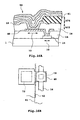
- Figs. 9A, 9B, and 9C are diagrams respectively showing the cross sectional structure along the lines A-A, B-B, and C-C of Fig. 8.
- Figs. 10A and 10B are respectively a planer diagram and a cross sectional diagram of one pixel of the active matrix type organic EL panel according to a second embodiment of the present invention.
- Fig. 11 shows another example of a planer structure of one pixel of the active matrix type organic EL panel according to the second embodiment.
- Fig. 12 is a planer diagram of one pixel of the active matrix type organic EL panel according to a third embodiment of the present invention.
- Fig. 13 shows another example of a planer structure of one pixel of the active matrix type organic EL element according to the third embodiment.
- Fig. 14 shows yet another example of a planer structure of one pixel of the active matrix type organic EL panel according to the third embodiment.
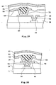
- Figs. 15A and 15B are diagrams respectively showing the cross sectional structure and planer structure of the contact section between the active layer 16 of the second TFT and the anode 52 of the organic EL element 50.
- Figs. 16A and 16B are diagrams respectively showing the cross sectional structure and planer structure of the contact section between the active layer 16 of the second TFT and the anode 52 of the organic EL element 50 according to a fourth embodiment of the present invention.
- Fig. 17 is a diagram showing another example of a cross sectional structure of the contact section between the active layer 16 of the second TFT and the anode 52 of the organic EL element 50 according to the fourth embodiment.
- Fig. 18 is a diagram showing a further example of across sectional structure of the contact section between the active layer 16 of the second TFT and the anode 52 of the organic EL element 50 according to the fourth embodiment.
- Fig. 19 is a diagram showing yet another example of a cross sectional structure of the contact section between the active layer 16 of the second TFT and the anode 52 of the organic EL element 50 according to the fourth embodiment.
- Fig. 20 is diagram showing another example of a cross sectional structure of the contact section between the active layer 16 of the second TFT and the anode 52 of the organic EL element 50 according to the third embodiment.
- Fig. 2 shows a circuit structure of one pixel in an active matrix type EL display device having m rows and n columns according to a first embodiment of the present invention.
- each pixel comprises an organic EL element 50, a switching TFT (first TFT) 10, an element driving TFT (second TFT) 20, and an storage capacitor Cs, and is constructed in a region surrounded by a gate line GL extending in the row direction and a data line DL extending in the column direction.
- a compensation TFT 30 having the conductive characteristic opposite of that of the second TFT 20 is provided between the power supply line VL and the second TFT 20.
- the gate and either the source or the drain of the compensation TFT 30 are connected to provide a diode connection.
- the diode is connected in the forward direction between the power supply line VL and the second TFT 20.
- the compensation TFT can be operated without supplying any designated control signal.
- the first TFT 10 is turned on by receiving a gate signal at its gate.
- the data signal supplied to the data line DL is held at the storage capacitor Cs connected between the first and second TFTs 10 and 20, and the potential at one electrode of the storage capacitor Cs becomes equal to the data signal.
- the second TFT 20 is provided between the power supply line VL and the organic EL element (the anode of the element) 50, and operates to supply a current corresponding to the voltage value of the data signal applied to its gate, from the power supply line VL to the organic EL element 50.
- an nch-TFT which is capable of high-speed response is used for the first TFT 10 and a pch-TFT is used for the second TFT 20.
- An nch-TFT having a polarity opposite that of the second TFT 20 is used for the compensation TFT 30.
- I-V (current-voltage) characteristic of the second TFT 20 is varied, the I-V characteristic of the compensation TFT 30 is varied in the opposite direction, thus compensating for the characteristic variation of the second TFT 20.
- Fig. 3 shows I-V characteristics of an nch-TFT and a pch-TFT which use polycrystalline silicon for the active layer.
- thench-TFT when the voltage applied to the gate exceeds a predetermined positive voltage(+Vth), the current value is rapidly increased.
- thepch-TFT when the voltage applied to the gate becomes less than a predetermined negative voltage (-Vth), the current value is rapidly increased.
- the threshold value, +Vth of the nch-TFT is varied by an increase, that is, shifted to the right in Fig.
- the threshold value, -Vth, of the pch-TFT is shifted by about the same degree to the right of Fig. 3.
- the threshold value, +Vth, of the nch-TFT is shifted to the left
- the threshold value, -Vth, of the pch-TFT is also shifted to the left.
- the amount of current supplied to the organic EL element 50 under the same condition would immediately be reduced.
- the amount of current flowing from the compensation TFT 30, which is provided between the second TFT 20 and the power supply line VL and which is constructed from an nch-TFT is increased.
- a second TFT 20 and a compensation TFT 30 of opposite polarity are provided between the power supply line VL and the organic EL element 50.
- the two TFTs are thus balanced. That is, the amounts of current flowing from these TFTs always compensate for each other.
- the maximum current value which can be supplied to the organic RL element 50 is less than that in the conventional circuit structure shown in Fig. 1 which does not have the compensation TFT 30.
- the identification sensitivity of human eyes at a high brightness is significantly lower than that at an intermediate brightness, a small reduction in the maximum current value which can be supplied does not significantly influence the display quality.
- the second TFT 20 and the compensation TFT 30 adjust the current flowing from each other in each pixel, the variation in the amount of current supplied to the organic EL element 50 among the pixels can be reduced.
- Fig. 4A shows the relationship between the applied voltage (data signal) and the illumination brightness for an example case where the organic EL element is illuminated by the pixel circuit structure of the first embodiment shown in Fig. 2.
- Fig. 4B shows the relationship between the applied voltage (data signal) and the illumination brightness for an example case wherein the organic EL element is illuminated by the conventional pixel circuit structure shown in Fig. 1.
- the setting in both Figs. 4A and 4B is such that the requested maximum brightness with respect to the organic EL element occurs at the applied voltage (data signal) of 8V, and the gradation display is performed at an applied voltage between 8V and 10V.
- Figs. 4A and 4B respectively indicate illumination brightness characteristics for cases wherein organic EL panels having circuit structure respectively of Fig. 2 and Fig. 1 are formed under different manufacturing conditions. In other words, these samples indicate illumination brightness characteristics for cases where the characteristic of the TFT in the pixel section is deliberately varied.
- the brightness (luminance) characteristics for the three samples having different characteristics for TFT in the pixel section significantly differ from each other at the set voltage range for data signals between 8V and 10V.
- the circuit structure according to the first embodiment although the characteristics differ from each other at the high-brightness region to which human eyes are insensitive, the brightness characteristic difference among the three samples at the intermediate-brightness region is very small.
- the variation can be compensated by the compensation TFT 30 of an opposite polarity, thus enabling inhibition of the variation in the illumination brightness of the organic EL element.
- Fig. 5 shows another example circuit structure according to the first embodiment.
- the circuit structure of Fig. 5 differs from that of Fig. 2 in that the second TFT 22 is constructed using an nch-TFT and the compensation TFT 32 is constructed using a diode connected pch-TFT. Similar to the above structure, with this structure, the variation in characteristic of the second TFT 22 can be compensated by the compensation TFT 32.
- Fig . 6 shows yet another example of a circuit structure according to the first embodiment.
- the circuit structure of Fig. 6 differs from that of Fig. 2 in that a plurality of second TFTs are provided in parallel between the compensation TFT 30 and the organic EL element 50.
- the polarity of the TFTs are identical to that in Fig. 2, that is, the second TFTs 24 are of pch and the compensation TFT 30 is of nch.
- the gates of two second TFTs 24 are both connected to the first TFT 10 and to the first electrode of the storage capacitor Cs.
- Each of the sources is connected to the compensation TFT 30 and each of the drains is connected to the organic EL element 50. In this manner, by providing a plurality of the second TFTs 24 in parallel, it is possible to further reduce the variation in the current supplied to the organic EL element due to the characteristic variation of the second TFT.
- the target current value for each of the two second TFTs 24 is assumed to be i, the total target current value for the two second TFTs 24 would be 2i. Even when the current supply capability for one of the second TFTs 24 is reduced to i/2 due to, for example, variations, the other second TFT 24 can continue to flow a current of i, and a total current of (3/2)i can be supplied to the organic EL element, where the target value is 2i. In the worst case, if the current supply capability of one of the TFTs becomes 0, a current of i can be supplied to the organic EL element by the other TFT in the example shown in Fig. 6. The advantage of such a structure can be readily seen when one considers a case wherein the current supply capability becomes 0 in a circuit having single second TFT 24 and the pixel becomes deficient.
- Each TFT in the first embodiment is obtained by polycrystallizing an a-Si by a laser annealing process.
- a plurality of second TFTs 24 are provided in parallel, it is easy to arrange the positions of the second TFTs 24 so that the laser is not simultaneously irradiated to active layers of both second TFTs 24 by, forexample, shifting the formation positions with respect to the laser scan direction.
- the probability that all second TFTs 24 become deficient can be significantly reduced, and thus, characteristic variation caused by the laser annealing can be minimized.
- a compensation TFT 30 is provided between the second TFTs 24 and the power supply line VL, even when there is a shift in the threshold value of the second TFTs 24 due to the variations in conditions such as, for example, annealing condition, the shift can be alleviated by the compensation TFT 30.
- Fig. 7 shows a further example pixel circuit structure according to the first embodiment.
- This circuit structure differs from that shown in Fig. 6 in that not only are the second TFTs 24 provided in plurality, but that the compensation TFTs are also provided in plurality.
- Each compensation TFT 34 is provided between the power supply line VL and the second TFTs 24.
- variations in the current supply capability generated among the compensation TFTs 34 can be alleviated and, thus, reliability of reduction in variation in current supply capability to the organic EL element 50 can be enhanced.
- Fig. 8 shows one example of the planer structure of the organic EL display device having a circuit structure shown in Fig. 7.
- Fig. 9A is a schematic cross section along the A-A line in Fig. 8
- Fig. 9B is a schematic cross section along the B-B line in Fig. 8
- Fig. 9C is a schematic cross section along the C-C line in Fig. 8.
- the layers (films) that are simultaneously formed are assigned the same reference numeral except where their functions are different.
- each pixel includes a first TFT 10, a storage capacitor Cs, two pch-second TFTs 24, two nch-compensation TFTs 34 which are diode-connected between the power supply line VL and the second TFTs 24, and an organic EL element 50 connected to the drains of the second TFTs 24.
- a pixel is placed in the region surrounded by a gate line GL extending in the row direction and a power supply line VL and a data line DL both extending in the column direction. Also in the example of Fig.
- delta arrangement is employed for realizing a more high resolution color display device wherein the positions for R, G, and B pixels are shifted at each row, and consequently, the data line DL and the power supply line VL are not straight, but extend in the column direction through the gap between pixels having positions shifted for each row.
- the first TFT 10 is formed near the cross section between the gate line GL and data line DL.
- an active layer 6 p-Si obtained by polycrystallizing a-Si by a laser annealing process is used.
- the active layer 6 has a pattern where it steps over twice the gate electrode 2 which protrudes from the gate line GL.
- a single gate structure is shown in Fig. 7, in the circuit, a dual gate structure is employed.
- the active layer 6 is formed on a gate insulation film 4 which is formed to cover the gate electrode 2.
- the sections of the active layer 6 immediately above the gate electrodes 2 form channels and source region 6S and drain region 6D to which an impurity is doped are formed around the channels. Because it is desirable that the first TFT 10 responds quickly to the selection signal output on the gate line GL, impurity such as phosphorous (P) is doped into the source region 6S and the drain region 6D, to form an nch-TFT.
- impurity such as phosphorous (P
- the drain region 6D of the first TFT 10 is connected, via a contact hole opened in an interlayer insulation film 14 formed to cover the entire first TFT 10, to the data line DL formed on top of the interlayer insulation film 14.
- the source region 6S of the first TFT 10 is connected to the storage capacitor Cs.
- the storage capacitor Cs is formed in the region where a first electrode 7 and a second electrode 8 are overlapped with the gate insulation film 4 in between.
- the first electrode 7 extends in the row direction in Fig. 8, similar to the gate line GL, and is formed integrally with a capacitor line SL formed from the same material as the gate.
- the second electrode 8 is integral with the active layer (semiconductor layer) 6 of the first TFT 10 and is constructed by the active layer 6 extending to the formation position of the first electrode 7.
- the second electrode 8 is connected to the gate electrodes 25 of the second TFTs 24 via a connector 42.
- the cross sectional structures for the two pch-second TFTs 24 and the two nch-compensation TFTs 34 are shown in Fig. 9B.
- the second TFTs 24 and the compensation TFTs 34 use a semiconductor layer 16 patterned in an island-like manner for each TFT in the direction along the data line DL (power supply line VL), as an active layer. Therefore, in this example, the channels of the second TFTs 24 and of the compensation TFTs 34 are arranged so that the channel length direction is along the data line DL, that is, along the longitudinal direction of the pixel having an elongated shape.
- the semiconductor layer 16 is simultaneously formed with the active layer 6 of the first TFT 10, and a polycrystalline silicon formed by polycrystallizing a-Si by a laser annealing process is used as the semiconductor layer 16.
- the compensation TFTs 34 placed at both ends of Fig. 9B are connected at their respective drain region to the same power supply line VL via a contact hole opened in the interlayer insulation film 14.
- a gate electrode 35 is provided immediately below the channel region of the compensation TFT 34 with the gate insulation film 4 in between.
- the gate electrode 35 is a layer formed by the same material as and simultaneously with the gate line GL, and is connected to the power supply line VL at a contact hole, as shown in Fig. 8. Therefore, the compensation TFTs 34 construct diodes in which both gates and drains are connected to the power supply line VL, as shown in the circuit diagram of Fig. 7.
- the source region of each compensation TFT 34 is provided to be distant from the source region of the second TFT 24 constructed from a pch-TFT, and is connected to the source region of the second TFT 24 by a contact wiring 43.
- each gate electrode 25 of the second TFTs 24 is a conductive layer formed from the same material as and simultaneously with the gate line GL.
- the conductive layer is connected to the second electrode 8 of the storage capacitor Cs via the connector 42, extends from the formation region of the storage capacitor Cs along the power supply line VL, extends further under the active layer 16, and forms each of the gate electrodes 25 of the two second TFTs 24.
- the organic EL element 50 has a cross sectional structure as shown in, for example, Fig. 9C, and is formed on top of a flattening insulation layer 18 provided over entire substrate for flattening the upper surface after each of the TFTs are formed as described above.
- the organic EL element 50 is constructed by laminating an organic layer between an anode (transparent electrode) 52 and a cathode (metal electrode) 57 formed at the uppermost layer and common to all pixels .
- the anode 52 and the source region of the second TFT 24 are not directly connected, but are connected via a connector 40 which constructs a wiring layer.
- two second TFTs 24 are both connected to a connector 40 and the connector 40 contacts the first electrode 52 of the organic EL element 50 at one contact point.
- the organic EL element 50 is connected to n second TFTs 24 at contact points having the number equal to or smaller than (n-1). Because the contact region sometimes become a non-illuminating region, by minimizing the number of contact points between the organic EL element 50 and the connector 40 (second TFTs 24), it is possible to maximize the illumination region. Another example related to the number of contacts will be described later as a third embodiment.
- the connection position between the connector 40 and the anode 52 is arranged so that it is shifted from the connection position between the connector 40 and the second TFTs 24.
- the emissive element layer 51 which will be described later and which includes an organic compound, electric field concentration tends to occur at a locally thin region, and degradation may be caused from the region where electric field concentration occurred. Therefore, it is desirable that the formation region of the emissive element layer 51 in which an organic material is used be as flat as possible.
- a recess due to the contact hole is produced, and the depth of the recess becomes larger as the contact hole becomes deeper.
- the contact hole for connecting the connector 40 and the source region of the second TFTs 24 at a region outside the formation region of the anode 52, it is possible to make the upper surface of the anode 52 onto which an organic layer is formed as flat as possible.
- An example for flattening the upper surface of the anode 52 will be described later to illustrate a fourth embodiment of the present invention.
- the emissive element layer (organic layer) 51 comprises, from the side of the anode, for example, a first hole transport layer 53, a second hole transport layer 54, an organic emissive layer 55, and an electron transport layer 56 laminated in that order.
- the first hole transport layer 52 includes MTDATA:4,4',4"-tris(3-methylphenylphenylamino)triphenylamine
- the second hole transport layer 54 includes TPD:N,N'-diphenyl-N,N'-di(3-methylphenyl)-1,1'-biphenyl-4,4'-diamine
- the organic emissive layer 55 includes, although dependent on the target illumination color of R, G, and B, for example, BeBq 2 :bis(10-hydroxybenzo[h]quinolinato)beryllium which includes quinacridone derivative
- the electron transport layer 56 is constructed from BeBq.
- the layers (53, 54, 56, and 57) other than the anode 52 constructed from an ITO (indium Tin Oxide) or the like and the organic emissive layer 55 are formed to be common to every pixel.
- Another example of the structure of the EL element can be constructed by sequentially laminating the layers of (a) transparent layer (anode); (b) a hole transport layer constructed from NBP; (c) an emissive layer including red (R) constructed by doping a reddopant (DCJTB) into a host material (Alq 3 ), green (G) constructed by doping a green dopant (coumarin 6) into a host material (Alq 3 ), and blue (B) constructed by doping a blue dopant (perylene) into a host material (BAlq) ; (d) an electron transport layer constructed fromAlq 3 ; (e) an electron injection layer constructed from lithium fluoride (LiF); and (f) electrode (cathode) constructed from Aluminum (
- a current based on the data signal can be accurately supplied to the organic EL element 50 for each pixel and, thus, uniform display without variation can be achieved.
- a plurality of (in this example, two) compensation TFTs 34 and second TFTs 24 are provided between the power supply line VL and the organic EL element 50 in that order, when a characteristic shift or deficiency is generated at one of these TFTs due to a variation, the variation in the supplied amount of current, which is determined by the total of the plurality of groups, is alleviated due to the presence of the other TFT having normal characteristics.
- a polycrystalline silicon layer produced by polycrystallization by laser annealing process is used as the active layers.
- the annealing process may be performed, for example, by scanning a laser beam which is longer in the row direction of the figure, in the column direction. Even in such a case, the channel direction of the first TFT 10 and the length channel direction of the active layers of each of the second and compensation TFTs 24 and 34 do not coincide, and the formation positions for the first and second TFTs 10 and 24 are far apart. Therefore, it is possible to prevent simultaneous generation of failures in the first and second TFTs 10 and 24 and in the second and compensation TFTs 24 and 34 by the laser annealing.
- first TFT 10, second TFTs 24, and compensation TFTs 34 are described as a bottom gate structure, but these TFTs can have a top gate structure wherein the gate electrode is formed on an upper layer than the active layer.
- the first embodiment it is possible to alleviate variations in characteristic of the transistor for supplying power to an element to be driven such as an organic EL element and, thus, it is possible to average the variation in the supplied power to the element to be driven and to prevent variations in illumination brightness (luminance) or the like at the element to be driven.
- a compensation thin film transistor having an opposite conductive characteristic as the element driving thin film transistor is provided in order to prevent variation in the illumination brightness among pixels as a result of characteristic variations in the transistor.
- the variation in the illumination brightness among pixels is inhibited by considering the placement of the element driving thin film transistor (second TFT) .
- Figs. 10A and 10B show an example configuration of one pixel according to the second embodiment.
- Fig. 10A is a schematic planer view
- Fig. 10B is a cross sectional view along the B-B line in Fig. 10A. This structure is shown with the same circuit structure as that of Fig. 1.
- the components corresponding to those in the drawings that are already explained will be referred to by the same reference numerals.
- one pixel comprises an organic EL element 50, a first TFT (switching thin film transistor) 10, a storage capacitor Cs, and a second TFT (element driving thin film transistor) 20.
- a single second TFT 20 is formed between the power supply line VL and the organic EL element 50, and the second TFT 20 is placed so that its channel length direction is along the longitudinal direction of the pixel formed in an elongated shape, similar to the configuration shown in Fig. 8.
- the illumination region of the organic element 50 can be maximized, and, at the same time, the necessary TFT can be efficiently placed in one pixel region which has a limited area, even in the case where a second TFT 20 having a long channel length is to be placed or in the case where a second TFT 20 and a compensation TFT 30 must be placed between the power supply line VL and the organic EL element 50 as shown in Fig. 8.
- the channel length of the second TFT 20 can be lengthened to a sufficient length, as shown in Figs. 10A and 10B.
- the reliability can be improved because the durability of the TFT is improved.
- this configuration enables averaging of the transistor characteristic of the second TFT 20, and, thus enables reduction in variations in the current supply capability of the second TFT 20 among pixels. The reduction of capability variation then allows for significant reduction of the variation in the illumination brightness of the organic EL element 50 caused by such a capability variation.
- the second TFT 20 uses a polycrystalline silicon layer obtained by polycrystallizing an amorphous silicon layer by laser annealing as the semiconductor layer (active layer) 16, similar as in the first embodiment.
- the scan direction of the laser annealing to coincide with the channel length direction of the second TFT 20, that is, by placing the irradiating region of the pulse laser so that the edge in the longitudinal direction crosses in the width direction of the channel 16c and by lengthening the channel length of the second TFT 20 as described above
- the characteristics variation in the second TFT 20 can be reduced because it is easy to adjust the laser so that the entire channel region of the second TFT 20 is not annealed by a single laser shot, and because generation of a large difference in the characteristic of the second TFT 20 among other pixels can be prevented.
- the second TFT 20 supplies a relatively large current from the driving power supply (power supply line VL) to the organic EL element 50.
- the driving power supply power supply line VL
- the second TFT 20 is directly connected to the power supply line VL, the required durability is high, and consequently, it is often desired that the channel length CL be longer than the channel width.
- the channel length of the second TFT 20 be lengthened to a sufficient length.
- the shape of each of the pixels tends to be designed to have a shape that is longer in the column direction as shown in Figs. 8 and 10A.
- the channel length would be along the longitudinal direction of the pixel region, and thus, the desired channel length as described above can be easily secured.
- a data line DL for supplying a data signal to the first TFT 10 is provided in the column direction and a selection line (gate line) GL is provided in the row direction.
- a selection line (gate line) GL is provided in the row direction.
- the second TFT 20 is arranged so that its channel length direction coincides with the scan direction of the laser annealing or is parallel to the column direction (extension direction of the data line DL), but the first TFT 10 is placed so that its channel length direction coincides with the extension direction of the gate line GL, that is, the row direction.
- the first TFT 10 and the second TFT 20 have different channel length directions.
- Fig. 10B shows a cross sectional structure of the second TFT 20 and the organic EL element 50 which is connected to the second TFT 20.
- the first TFT 10 which is not shown, has a basic structure similar to that of the second TFT 20 shown in Fig. 10B, with the exceptions that the first TFT 10 has a different channel length, a double gate structure, and a different conductive type for the active layer 6.
- the first TFT and second TFT shown in the first embodiment both have a bottom gate structure, but the first TFT 10 and the second TFT 20 of the second embodiment have a top gate structure wherein the gate electrode is formed on an upper layer than the active layer.
- the structure of the second embodiment is not limited to the top gate structure, and a bottom gate structure may also be employed.
- the active layer 16 of the second TFT 20 and the active layer 6 of the first TFT 10 are both constructed from polycrystalline silicon obtained by laser annealing and polycrystallizing an amorphous silicon layer formed on a substrate 1, as described above.
- a gate insulation film 4 is formed on top of the active layers 6 and 16 constructed form polycrystalline silicon.
- Each of the gate electrodes 2 and 25 respectively of the first TFT 10 and of the second TFT 20 is formed on the gate insulation film 4.
- the gate electrode 25 of the second TFT 20 is connected to the second electrode 8 of the storage capacitor Cs which is integral with the active layer 6 of the first TFT 10. As shown in Fig. 10A, the gate electrode 25 is patterned so that it extends from the connection section with the storage capacitor Cs in the column direction and widely covers the section of the gate insulation film 4 above the active layer 16.
- the region of the active layer 16 of the second TFT 20 which is covered by the gate electrode 25 at the top is the channel region 16c.
- a source region 16s and a drain region 16d are formed at both sides of the channel region 16c.
- the source region 16s of the active layer 16 is electrically connected to the power supply line VL near the storage capacitor Cs via a contact hole formed to penetrate through the gate insulation film 4 and the interlayer insulation film 14.
- the drain region 16d is connected to a connector (wiring layer) 40 near the gate line GL which corresponds to the next row of the matrix, via a contact hole formed to penetrate through the gate insulation film 4 and the interlayer insulation film 14.
- the connector 40 extends from the connection region with the drain region 16d to the formation region of the organic EL element 50, and is electrically connected to an ITO electrode (anode) 52 of the organic EL element 50 via a contact hole formed on a first flattening insulation layer (planarizating insulation layer) 18 which is formed to cover the interlayer insulation film 14, power supply line VL, and connector 40.
- FIG. 10B only the central region of formation of the anode 52 of the organic EL element is opened above the first flattening layer 18.
- a second flattening (planarizating) insulation layer 61 is formed to cover the edge of the anode 52, wiring region, and the formation regions for the first and second TFTs.
- the emissive element layer 51 of the organic EL element 50 is formed on the anode 52 and the second flattening insulation layer 61.
- a metal electrode 57 which is common to all pixels is formed on top of the emissive element layer 51.
- the channel length CL of the second TFT 20 is sufficiently long.
- the moving pitch P of the laser and the channel length CL are adjustable according to the setting of the optical assembly system of the laser annealing device or the like. In such a case, it is preferable that the device be adjusted so that CL > P. In a display device having a resolution of about 200 dpi, for example, even when the length in the pixel row direction is about 30 m, about 80 m can be secured in the column direction.
- the channel region 16c of the second TFT 20 is always polycrystallized by a plurality of pulse laser irradiations, and it is possible to reduce the difference in the characteristic from the second TFT 20 of other pixels which are similarly polycrystallized by a plurality of pulse laser irradiations.
- a single second TFT 20 is formed between the organic element 50 and the power supply line VL in one pixel.
- the second embodiment is not limited to such a configuration, and a plurality of second TFTs 20 may be provided in one pixel.
- Fig. 11 shows an example layout for a case wherein a plurality of second TFTs 20 are connected in parallel between the power supply line VL and the organic EL element 50.
- the equivalent circuit of the pixel structure shown in Fig. 11 is similar to the case where the compensation TFT 30 is removed from the circuit shown in Fig. 6.
- the source regions 16sa and 16sb of two second TFTs 20 are both connected to the power supply line VL and the drain regions 16da and 16db are both connected to the anode 52 of the organic EL element 50 via a contact 40 respectively.
- the placement of two second TFTs 20a and 20b is such that the channel length direction of the second TFTs 20a and 20b is approximately parallel to the longitudinal direction (in this case, this direction coincides with the extension direction of the data line DL) of the pixel region similar to Fig. 10A. With such a placement, it is possible to maximize the illumination region and, at the same time, to secure maximum length for each channel length CL.
- the scan direction of the laser anneal is set, even in Fig. 11, to be parallel to both channel length directions of the two second TFTs 20a and 20b.
- the active layers 16a and 16b are placed in a straight line.
- the active layers for a plurality of second TFTs 20a and 20b be provided on a straight line, but because the channel regions 16ca and 16cb of the second TFTs 20a and 20b do not completely coincide with the laser scan direction and are somewhat shifted, it is possible to more reliably prevent the characteristics of the TFTs 20a and 20b to vary in the same manner.
- the probability that the channel for the two TFTs are simultaneously annealed by the same pulse is reduced and, thus, the probability of a problem such as, for example, the characteristics of the second TFTs 20a and 20b being shifted from the set value in the same manner or simultaneous failure of both transistors can be significantly lowered. Therefore, the variation in the total amount of current supplied to the organic EL element 50 among the pixels can be reduced.
- both channel lengths CLa and CLb of the two second TFTs 20a and 20b be greater than the moving pitch P of the laser, as described above.
- the separation distance L between the channels 16ca and 16cb of the plurality of second TFTs 20a and 20b be greater than the moving pitch P of the laser.
- the second embodiment it is possible to alleviate variations in characteristics of the transistor for supplying power to an element to be driven such as an organic EL element, and thus, it is possible to average the variation in the supplied power to the element to be driven and to prevent variations in illumination brightness or the like at the element to be driven.
- Amethod for efficiently connecting a plurality of second TFTs 20 and corresponding organic EL element 50 within one pixel will now be described as a third embodiment of the present invention.
- provision of a plurality of second TFTs 20 between an organic EL element 50 and a power supply line VL within one pixel is advantageous from the viewpoint of improvements in reliability, characteristic, or the like.
- a current can more reliably be supplied from the power supply line VL to the organic EL element 50 via the second TFTs 20.
- the contact section usually has a light blocking characteristic.
- the connection between the organic El element 50 and the second TFT 20 is achieved by the wiring layer 40 (connector) which is a metal wiring, and at the contact section between the wiring layer 40 and the anode 52, the wiring layer 40 having a light blocking characteristic is present below the anode 52.
- the light from the emissive layer 55 cannot pass through to the side of the substrate 1. Therefore, if n contact sections are provided between the second TFTs 20 and the organic EL element 50 to correspond to the n second TFTs 20, the illumination area would be reduced in proportion to the number of contacts.
- the number of contacts between the second TFTs 20 and the organic EL element 50 is less than or equal to (n-1), wherein the number of second TFTs 20 in one pixel is n (n.2).
- n second TFTs 20 and the organic EL element 50 are connected with the number of contacts being equal to or less than (n-1).
- Fig. 12 shows a contact method between second TFTs 20a and 20b and an organic EL element 50 when two second TFTs 20a and 20b are provided in parallel between the power supply line VL and the organic EL element 50. Similar to Fig. 11, the two TFTs 20a and 20b are placed such that respective channel length direction is parallel to the longitudinal direction of the pixel (the extension direction of the data line DL) or to the scan direction of laser annealing. The TFTs 20a and 20b are also placed so that they are shifted from each other. With such a configuration, as described above, the illumination variation among pixels can be reduced and the reliability can be improved.
- a semiconductor layer constructed from p-Si patterned into a single island-like manner is used for the active layers 16a and 16b of the second TFTs 20a and 20b.
- the semiconductor is patterned so that both ends in the column direction are the source regions (in the case of a pch-TFT) 16sa and 16sb of respective second TFTs 20a and 20b, and are connected to the power supply line VL.
- the region around the center of the semiconductor pattern defines the drain regions (in the case of a pch-TFT) 16da and 16db of the TFTs 20a and 20b, and the drain regions are connected to a single wiring layer 40 provided between the two TFTs via a common contact hole formed to penetrate through the interlayer insulation film 14 and the gate insulation film 4 (refer to Fig. 10B).
- the wiring layer 40 extends to the anode formation region of the organic EL element 50. Similar to the cross sectional structure shown in Fig. 10B, the wiring layer 40 is connected to the anode 52 of the organic EL element 50 via one contact hole opened on the first flattening insulation layer 18.
- the connection position between the wiring layer 40 and the anode 52 is set in Fig. 12 to be around the center of the anode 52 in the longitudinal direction of the pixel.
- the contact position is not limited to the configuration of Fig. 12, but by placing the contact position near the center of the anode 52 as shown in Fig.
- averaging effect of the current density can be obtained in the formation region of the anode 52 which is constructed from an ITO or the like having a relatively high resistance compared to a metal electrode and, thus, the uniformity of the illumination brightness at the illumination surface of each pixel can be improved.
- the number of second TFTs 20 is increased to three.
- Three second TFTs 20-1, 20-2, and 20-3 are connected in parallel between the power supply line VL and the anode of the organic EL element 50.
- the active layer 16 of three second TFTs 20 are integrally formed and are set so that the channel length direction is along the row direction in Fig. 13.
- Each of the channel regions 16c 1 through 16c 3 of second TFTs 20-1 through 20-3 are separated in their channel width directions by openings in the pattern of the active layer 16.
- the three second TFTs 20 are connected to the power supply line VL at one contact point, and also connected to the anode 52 of the organic EL element 50 at one contact point by a single wiring layer 40.
- the gate electrode 25 is common to all three TFTs, is electrically connected to the second electrode 8 of the storage capacitor Cs, and is constructed from a metal wiring extending in the column direction from around the storage capacitor Cs.
- three second TFTs 20-1 through 20-3 are connected to the organic EL element 50 by one contact section. Therefore, the ratio of the occupational area of the contact section within the formation region of the organic EL element 50 can be lowered, and thus, the ratio of opening in one pixel, that is, the illumination area, can be increased.
- the number of second TFTs 20 is increased to 4.
- the four TFTs 20-1 through 20-4 are electrically connected in parallel between the power supply line VL and the anode 52 of the organic EL element 50.
- the active layer 16 of four second TFTs 20 are integrally constructed and the channel length directions of the TFTs 20-1 through 20-4 are set to be parallel to the longitudinal direction of the pixel region or the extension direction of the data line DL, similar to Fig. 12.
- the four TFTs are arranged in an almost straight line.
- TFTs 20-1 through 20-4 are connected to the power supply line VL at three contact points, and connected to the anode 52 of the organic EL element 50 at two contact points by first and second wiring layers 40-1 and 40-2.
- the source regions 16S 1 and 16S 4 of the TFTs 20-1 and 20-4 which are located at the outermost positions of the single active layer 16 are respectively connected to the power supply line VL as a separate entity.
- the source regions 16S 2 and 16S 3 of the TFTs 20-2 and 20-3 which are located at the central position are together connected to the power supply line VL.
- the second TFTs 20-1 and 20-2 and the organic EL element 50 are connected as follows.
- the drain regions 16d 1 and 16d 2 of the second TFTs 20-1 and 20-2 are connected to a first wiring layer 40-1 extending from between the second TFTs 20-1 and 20-2 to the element 50, and the first wiring layer 40-1 extends to the formation region of the organic EL element 50 and is connected to the anode 52 of the element.
- the second TFTs 20-3 and 20-4 are connected to the organic EL element 50 as follows.
- the drain regions 16d 3 and 16d 4 of the second TFTs 20-3 and 20-4 are connected to a second wiring layer 40-2 extending from between the second TFTs 20-3 and 20-4 to the element 50, and the second wiring layer 40-2 extends to the formation region of the organic EL element 50 and is connected to the anode 52 of the element.
- four second TFTs 20-1 through 20-4 are connected to the organic EL element 50 only at two contact points, in order to inhibit the reduction of illumination region caused by providing four second TFTs 20-1 through 20-4.
- the third embodiment by connecting an element to be driven and a transistor for supplying power to the element by minimum number of contacts, necessary transistors and elements can be efficiently placed in a limited area. Therefore, when an EL element is used, for example, as the element to be driven, the illumination area ratio can be improved in one pixel unit.
- connection structure between the second TFT 20 and the organic EL element 50 will now be described referring to Figs. 15 through 20.
- the contact region between the organic EL element 50 and the second TFT 20 is usually a non-illuminating region. Also, in order to improve the integration density in many integrated circuits, and in order to improve the resolution in a display device, it is desired to minimize the contact area.
- the active layer 16 of the second TFT 20 is directly connected to the anode 52 of the organic EL element 50 or when the direct connection is not employed and a metal connection layer (Al layer, Cr layer or the like) is provided in between for improving the connection characteristic, it is preferable to form the first contact hole 70 of the interlayer insulation film 14 and the second contact hole 72 of the first flattening insulation layer 18 to overlap each other, as shown in Figs. 15A and 15B.
- the total step size (h70 + h72) of the contact holes become large and, thus, the surface flatness of the layer formed on top of the contact hole is reduced.
- a second flattening insulation layer 61 is used for covering the edge region of the anode 52 as shown in Fig. 15A in order to prevent shortage between the anode 52 and the cathode 57 caused by coverage failure of the emissive element layer 51 at the anode edge region.
- the second flattening (planarizating) insulation layer 61 is opened at the central region of the anode 52.
- the opened section of the second flattening insulation layer 61 is formed near the first and second contract holes 70 and 72, and the formation surface of the emissive element layer 51 will be influenced also by the step h74 caused by the opening of the second flattening insulation layer 61.
- the organic EL element 50 In the organic EL element 50, on the other hand, illumination organic compound in the emissive layer 55 is illuminated by flowing a current through the emissive element layer 51. It is known that if there is a large difference in the thickness within the layer of the emissive element layer 51, an electric field concentration tends to occur at a portion that is thinner than the other portions, and a dark spot tends to be generated at such a portion. Dark spots degrade display quality, and furthermore, because dark spots tend to expand as the element is driven, each dark spot shortens the life of the element. Therefore, when the organic EL element 50 is formed at a layer above the contact region, it is desired to maximize the flatness of the formation surface of the emissive element layer 51.
- the contact structure shown in Figs. 15A and 15B in which the emissive element layer 51 is formed on an uneven surface is not desirable from the viewpoint of improving the reliability of the emissive element layer 51.
- Figs. 16A and 16B show an example of a connection method wherein the flatness at the formation surface of the emissive element layer 51 is increased, considering the above.
- Fig. 16A shows a cross sectional structure of the contact section between the active layer 16 of the second TFT 20 and the anode 52 of the organic EL element 50.
- Fig. 16B shows a schematic planer structure of the contact section.
- the connection structure shown in Figs. 16A and 16B is identical to the structure shown in Figs. 8 and 9 as explained for the first embodiment.
- connection position between the wiring layer 40 and the anode 52 is placed such that it is shifted with respect to the connection position between the wiring layer 40 and the active layer 16 of the second TFT 20.
- the anode surface at the contact region between the wiring layer 40 and the anode 52 being the formation surface of the emissive element layer 51, is only influenced by the step h72 caused by the second contact hole 72 and is not influenced by the step h70 caused by the first contact hole 70 as in the case shown in Figs. 15A and 15B. Therefore, as is clear from comparison between Figs. 15A, B and 16A, B, the flatness of the formation surface for emissive element layer, especially at the illumination region of each pixel onto which the emissive layer 55 is formed can be improved.
- Fig. 17 shows a method for further flattening the formation surface of the emissive element layer as shown in Fig. 16A.
- the formation position of the second contact hole 72 for connecting the wiring layer 40 and the anode 52 of the organic EL element 50 is shifted from the formation position of the first contact hole 70, and, in addition, the second contact hole 72 is covered by the second flattening insulation layer 61. Therefore, the region onto which the emissive layer 55 is formed is neither influenced by the step caused by the first contact hole 70 nor by the step caused by the second contact hole 72.
- the flatness of the formation surface of the emissive element layer can thus be further improved. Because the second flattening layer 61 covers the edge region of the anode 52, shortage between the anode 52 and the cathode 57 or the like can reliably be prevented.
- the illumination region of the organic EL element is a region in which the anode 52 and the cathode 57 oppose each other with the emissive layer 55 in between, and the region in which the second flattening insulation layer 61 is formed between the anode 52 and the emissive element layer 51 does not illuminate. Therefore, strictly speaking, with the configuration shown in Fig. 17, because the second flattening insulation layer 61 covers not only the edge of the anode 52 but also the section above the second contact hole 72, the illumination region is reduced. However, as described above, when the wiring layer 40 or the like which has a light blocking characteristic is formed at a lower layer, the formation region of the wiring layer 40 will be a non-illuminating region when seen from outside. Therefore, even when the structure shown in Fig. 17 in which the second flattening insulation layer 61 covers the second contact hole 72 is employed, the actual reduction in the illumination area due to the formation of the second flattening insulation layer 61 for one pixel can be inhibited.
- the improvement effect on the flatness of the formation surface for the emissive element layer can also be achieved by the method of covering the contact hole by the second flattening insulation layer 61, by employing a layout wherein the first and second contact holes 70 and 72 are placed to overlap each other, as in Figs. 15A and 15B.
- the active layer 16 of the second TFT 20 and the anode 52 of the organic EL element 50 are connected by first and second contact holes 70 and 72 formed to overlap each other, and the region of the anode 52 having the upper surface recessed because of two contact holes is covered by the second flattening insulation layer 61.
- the formation surface for the emissive element layer above the contact holes 70 and 72 will thus be a surface with a good flatness, formed by the second flattening insulation layer 61. Also, by placing the two contact holes 70 and 72 at the same position in Fig. 18, the element placement efficiency in one pixel is high and it is easy to contribute to an improvement in the illumination region.
- Fig. 19 shows another flattening method of the formation surface for the emissive element layer.
- the method of Fig. 19 differs from that of Fig. 17 in that a filling layer 62 is selectively formed on top of the anode 52 instead of the second flattening insulation layer 61, at the formation region of the second contact hole 72, in order to fill the recess caused by the contact hole.
- a filling layer 62 is selectively formed on top of the anode 52 for covering the contact hole 72, even when the second flattening insulation layer 61 or the like is not provided, the formation surface for the emissive element layer above the contact hole can be flattened.
- the filling layer 62 may also be employed, similar to Fig.
- the filling layer 62 is selectively formed on the anode 52 at the region where the two contact holes are formed to overlap, in order to fill the deep recess formed by the two contact holes.
- the emissive element layer 51 is formed on a flat surface of the filling layer 62 at the region where the contact hole or contact holes are formed and, thus, failures in the emissive element layer generating in this region can be prevented.
- the material for the second flattening insulation layer 61 and for the filling layer 62 can be any material which has a flat upper surface, but it is preferable to use a stable and insulating material which does not react with the emissive element layer 51 and which is not hydrous.
- a stable and insulating material which does not react with the emissive element layer 51 and which is not hydrous.
- polyimide, HMOSO, TOMCAT, or TEOS can be used.
- the flatness of the surface onto which the element to be driven such as an organic EL element, is formed can be improved, and thus, it is possible to improve the reliability of the element to be driven.
Landscapes
- Engineering & Computer Science (AREA)
- Physics & Mathematics (AREA)
- Microelectronics & Electronic Packaging (AREA)
- Computer Hardware Design (AREA)
- General Physics & Mathematics (AREA)
- Theoretical Computer Science (AREA)
- Geometry (AREA)
- Electroluminescent Light Sources (AREA)
- Devices For Indicating Variable Information By Combining Individual Elements (AREA)
- Control Of El Displays (AREA)
- Metal-Oxide And Bipolar Metal-Oxide Semiconductor Integrated Circuits (AREA)
- Thin Film Transistor (AREA)
- Recrystallisation Techniques (AREA)
- Control Of Indicators Other Than Cathode Ray Tubes (AREA)
Applications Claiming Priority (4)
| Application Number | Priority Date | Filing Date | Title |
|---|---|---|---|
| JP2000300982 | 2000-09-29 | ||
| JP2000300982 | 2000-09-29 | ||
| JP2001279802 | 2001-09-14 | ||
| JP2001279802A JP4925528B2 (ja) | 2000-09-29 | 2001-09-14 | 表示装置 |
Publications (1)
| Publication Number | Publication Date |
|---|---|
| EP1193676A2 true EP1193676A2 (fr) | 2002-04-03 |
Family
ID=26601273
Family Applications (1)
| Application Number | Title | Priority Date | Filing Date |
|---|---|---|---|
| EP01308326A Withdrawn EP1193676A2 (fr) | 2000-09-29 | 2001-09-28 | Transistor à couche mince pour l'alimentation d'un élément électroluminescent |
Country Status (6)
| Country | Link |
|---|---|
| US (5) | US6781153B2 (fr) |
| EP (1) | EP1193676A2 (fr) |
| JP (1) | JP4925528B2 (fr) |
| KR (3) | KR100481110B1 (fr) |
| CN (1) | CN1242492C (fr) |
| TW (1) | TW526676B (fr) |
Cited By (21)
| Publication number | Priority date | Publication date | Assignee | Title |
|---|---|---|---|---|
| WO2003025894A2 (fr) * | 2001-09-18 | 2003-03-27 | Pioneer Corporation | Circuit d'attaque pour elements electroluminescents |
| FR2849534A1 (fr) * | 2002-12-31 | 2004-07-02 | Lg Philips Lcd Co Ltd | Dispositif d'affichage electroluminescent organique a matrice active et son procede de fabrication |
| FR2849961A1 (fr) * | 2002-12-26 | 2004-07-16 | Lg Philips Lcd Co Ltd | Dispositif d'affichage electroluminescent organique de type a panneau double, et procede de fabrication de celui-ci |
| WO2004061812A1 (fr) * | 2002-12-27 | 2004-07-22 | Semiconductor Energy Laboratory Co., Ltd. | Dispositif a semi-conducteur et ecran mettant ce dernier en application |
| KR100562261B1 (ko) * | 2002-07-31 | 2006-03-22 | 세이코 엡슨 가부시키가이샤 | 전자 회로, 전자 회로의 구동 방법, 전기 광학 장치, 전기광학 장치의 구동 방법 및 전자 기기 |
| US7158105B2 (en) | 2002-08-30 | 2007-01-02 | Seiko Epson Corporation | Electronic circuit, method of driving electronic circuit, electro-optical device, method of driving electro-optical device, and electronic apparatus |
| EP1793425A2 (fr) | 2005-11-30 | 2007-06-06 | Seiko Epson Corporation | Dispositif électroluminescent et appareil électronique |
| US7268498B2 (en) | 2004-04-28 | 2007-09-11 | Semiconductor Energy Laboratory Co., Ltd. | Display device |
| EP1884910A1 (fr) * | 2005-05-23 | 2008-02-06 | Sharp Kabushiki Kaisha | Substrat de matrice active, dispositif d' affichage, et procede de correction des defauts de pixels |
| US7365719B2 (en) | 2003-05-16 | 2008-04-29 | Semiconductor Energy Laboratory Co., Ltd. | Display device |
| EP2237253A1 (fr) * | 2009-04-01 | 2010-10-06 | ARISTOTLE UNIVERSITY OF THESSALONIKI- Research Committee | Circuit de pixels, affichage l'utilisant et son procédé de commande |
| US7928945B2 (en) | 2003-05-16 | 2011-04-19 | Semiconductor Energy Laboratory Co., Ltd. | Display device and driving method thereof |
| US8254865B2 (en) | 2006-04-07 | 2012-08-28 | Belair Networks | System and method for frequency offsetting of information communicated in MIMO-based wireless networks |
| US8280337B2 (en) | 2006-04-07 | 2012-10-02 | Belair Networks Inc. | System and method for zero intermediate frequency filtering of information communicated in wireless networks |
| US8324618B2 (en) | 2001-11-09 | 2012-12-04 | Semiconductor Energy Laboratory Co., Ltd. | Light emitting device |
| US8772789B2 (en) | 2005-11-30 | 2014-07-08 | Seiko Epson Corporation | Light-emitting device and electronic apparatus |
| EP1501067B1 (fr) * | 2002-04-26 | 2016-04-20 | Sanyo Electric Co., Ltd. | Afficheur |
| US9640558B2 (en) | 2005-06-30 | 2017-05-02 | Semiconductor Energy Laboratory Co., Ltd. | Semiconductor device, display device, and electronic appliance |
| US10546529B2 (en) | 2006-10-26 | 2020-01-28 | Semiconductor Energy Laboratory Co., Ltd. | Electronic device, display device, and semiconductor device and method for driving the same |
| WO2020025620A1 (fr) * | 2018-08-03 | 2020-02-06 | Osram Oled Gmbh | Dispositif d'éclairage optoélectronique et procédé de commande d'un dispositif d'éclairage optoélectronique |
| US11869977B2 (en) | 2013-09-13 | 2024-01-09 | Semiconductor Energy Laboratory Co., Ltd. | Semiconductor device |
Families Citing this family (188)
| Publication number | Priority date | Publication date | Assignee | Title |
|---|---|---|---|---|
| KR100637433B1 (ko) | 2004-05-24 | 2006-10-20 | 삼성에스디아이 주식회사 | 발광 표시 장치 |
| JP4925528B2 (ja) * | 2000-09-29 | 2012-04-25 | 三洋電機株式会社 | 表示装置 |
| US6912021B2 (en) * | 2001-01-22 | 2005-06-28 | Seiko Epson Corporation | Electro-optical device, method for driving electro-optical device, electronic apparatus, and method for driving electronic apparatus |
| JP4380954B2 (ja) * | 2001-09-28 | 2009-12-09 | 三洋電機株式会社 | アクティブマトリクス型表示装置 |
| US20030103022A1 (en) * | 2001-11-09 | 2003-06-05 | Yukihiro Noguchi | Display apparatus with function for initializing luminance data of optical element |
| CN101009322B (zh) * | 2001-11-09 | 2012-06-27 | 株式会社半导体能源研究所 | 发光器件 |
| KR100940342B1 (ko) | 2001-11-13 | 2010-02-04 | 가부시키가이샤 한도오따이 에네루기 켄큐쇼 | 표시장치 및 그 구동방법 |
| US7483001B2 (en) * | 2001-11-21 | 2009-01-27 | Seiko Epson Corporation | Active matrix substrate, electro-optical device, and electronic device |
| TWI250498B (en) * | 2001-12-07 | 2006-03-01 | Semiconductor Energy Lab | Display device and electric equipment using the same |
| CN101673508B (zh) * | 2002-01-18 | 2013-01-09 | 株式会社半导体能源研究所 | 发光器件 |
| JP3481231B2 (ja) * | 2002-03-05 | 2003-12-22 | 三洋電機株式会社 | 有機エレクトロルミネッセンス表示装置およびその製造方法 |
| JP3989763B2 (ja) * | 2002-04-15 | 2007-10-10 | 株式会社半導体エネルギー研究所 | 半導体表示装置 |
| TWI272556B (en) | 2002-05-13 | 2007-02-01 | Semiconductor Energy Lab | Display device |
| JP2003345306A (ja) * | 2002-05-23 | 2003-12-03 | Sanyo Electric Co Ltd | 表示装置 |
| JP4086550B2 (ja) * | 2002-05-30 | 2008-05-14 | 三洋電機株式会社 | 表示装置 |
| JP4813743B2 (ja) * | 2002-07-24 | 2011-11-09 | 株式会社 日立ディスプレイズ | 画像表示装置の製造方法 |
| JP3829778B2 (ja) | 2002-08-07 | 2006-10-04 | セイコーエプソン株式会社 | 電子回路、電気光学装置、及び電子機器 |
| TWI338346B (en) | 2002-09-20 | 2011-03-01 | Semiconductor Energy Lab | Display device and manufacturing method thereof |
| JP2004179138A (ja) * | 2002-10-01 | 2004-06-24 | Sanyo Electric Co Ltd | エレクトロルミネッセンス表示装置及びその製造方法 |
| KR100915233B1 (ko) * | 2002-11-05 | 2009-09-02 | 삼성전자주식회사 | 박막 트랜지스터 어레이 기판 |
| EP1566787A4 (fr) * | 2002-11-25 | 2009-12-09 | Toshiba Matsushita Display Tec | Panneau d'affichage organique electroluminescent |
| WO2004057561A1 (fr) * | 2002-12-19 | 2004-07-08 | Semiconductor Energy Laboratory Co., Ltd. | Procede de commande pour dispositif luminescent |
| TWI353467B (en) * | 2003-01-08 | 2011-12-01 | Samsung Electronics Co Ltd | Polysilicon thin film transistor array panel and m |
| KR100521277B1 (ko) * | 2003-02-05 | 2005-10-13 | 삼성에스디아이 주식회사 | 애노드전극층을 전원공급층으로 사용한 평판표시장치 및그의 제조방법 |
| EP1594347B1 (fr) * | 2003-02-13 | 2010-12-08 | FUJIFILM Corporation | Appareil d'affichage et procede de fabrication correspondant |
| EP1598938B1 (fr) | 2003-02-28 | 2013-10-30 | Semiconductor Energy Laboratory Co., Ltd. | Dispositif a semi-conducteurs et son mode de fonctionnement |
| KR100496297B1 (ko) * | 2003-03-06 | 2005-06-17 | 삼성에스디아이 주식회사 | 박막 트랜지스터를 구비한 평판표시장치 |
| EP1607931B1 (fr) * | 2003-03-26 | 2014-01-08 | Semiconductor Energy Laboratory Co., Ltd. | Substrat pour dispositif et dispositif electroluminescent |
| JP4562997B2 (ja) | 2003-03-26 | 2010-10-13 | 株式会社半導体エネルギー研究所 | 素子基板及び発光装置 |
| KR100528913B1 (ko) | 2003-04-29 | 2005-11-16 | 삼성에스디아이 주식회사 | 평판표시소자 |
| JP4518747B2 (ja) | 2003-05-08 | 2010-08-04 | 三洋電機株式会社 | 有機el表示装置 |
| JP4754772B2 (ja) * | 2003-05-16 | 2011-08-24 | 株式会社半導体エネルギー研究所 | 発光装置及び該発光装置を用いた電子機器 |
| US7557779B2 (en) | 2003-06-13 | 2009-07-07 | Semiconductor Energy Laboratory Co., Ltd. | Display device |
| US7122969B2 (en) * | 2003-06-18 | 2006-10-17 | Semiconductor Energy Laboratory Co., Ltd. | Element substrate and light emitting device |
| JP2005031629A (ja) | 2003-06-19 | 2005-02-03 | Sharp Corp | 表示素子および表示装置 |
| US8552933B2 (en) * | 2003-06-30 | 2013-10-08 | Semiconductor Energy Laboratory Co., Ltd. | Light emitting device and driving method of the same |
| JP4583732B2 (ja) * | 2003-06-30 | 2010-11-17 | 株式会社半導体エネルギー研究所 | 表示装置、及びその駆動方法 |
| KR100560780B1 (ko) | 2003-07-07 | 2006-03-13 | 삼성에스디아이 주식회사 | 유기전계 발광표시장치의 화소회로 및 그의 구동방법 |
| KR100560782B1 (ko) * | 2003-08-25 | 2006-03-13 | 삼성에스디아이 주식회사 | 유기 전계 발광 표시 장치 |
| JP2005123571A (ja) * | 2003-09-22 | 2005-05-12 | Sanyo Electric Co Ltd | トランジスタ基板、表示装置及びそれらの製造方法 |
| CA2443206A1 (fr) | 2003-09-23 | 2005-03-23 | Ignis Innovation Inc. | Panneaux arriere d'ecran amoled - circuits de commande des pixels, architecture de reseau et compensation externe |
| JP4413569B2 (ja) * | 2003-09-25 | 2010-02-10 | 株式会社 日立ディスプレイズ | 表示パネルの製造方法及び表示パネル |
| JP4443179B2 (ja) * | 2003-09-29 | 2010-03-31 | 三洋電機株式会社 | 有機elパネル |
| JP4488709B2 (ja) * | 2003-09-29 | 2010-06-23 | 三洋電機株式会社 | 有機elパネル |
| JP4446707B2 (ja) * | 2003-09-30 | 2010-04-07 | 三洋電機株式会社 | アクティブマトリクス型表示装置 |
| JP2005107890A (ja) | 2003-09-30 | 2005-04-21 | Sanyo Electric Co Ltd | El表示装置 |
| TWI252602B (en) * | 2003-10-09 | 2006-04-01 | Au Optronics Corp | Pixel structure of active organic light emitting diode |
| KR100552975B1 (ko) * | 2003-11-22 | 2006-02-15 | 삼성에스디아이 주식회사 | 능동 매트릭스 유기전계발광표시장치 및 그의 제조방법 |
| JP4678124B2 (ja) * | 2003-11-10 | 2011-04-27 | セイコーエプソン株式会社 | 電気光学装置、電気光学装置の製造方法及び電子機器 |
| KR100741962B1 (ko) | 2003-11-26 | 2007-07-23 | 삼성에스디아이 주식회사 | 평판표시장치 |
| JP4278499B2 (ja) * | 2003-12-01 | 2009-06-17 | 三菱電機株式会社 | 表示装置 |
| JP2005173881A (ja) | 2003-12-10 | 2005-06-30 | Sanyo Electric Co Ltd | El表示装置 |
| JP4581408B2 (ja) * | 2004-01-19 | 2010-11-17 | ソニー株式会社 | 表示装置 |
| KR100741966B1 (ko) * | 2004-01-27 | 2007-07-23 | 삼성에스디아이 주식회사 | 유기전계발광 표시장치 및 그의 제조방법 |
| US20050243032A1 (en) * | 2004-04-29 | 2005-11-03 | Kuo-Sheng Lee | Power line layout for electroluminescent display |
| US7199397B2 (en) * | 2004-05-05 | 2007-04-03 | Au Optronics Corporation | AMOLED circuit layout |
| CA2472671A1 (fr) | 2004-06-29 | 2005-12-29 | Ignis Innovation Inc. | Procede de programmation par tensions pour affichages a del excitees par courant |
| KR100699997B1 (ko) * | 2004-09-21 | 2007-03-26 | 삼성에스디아이 주식회사 | 다수개의 구동 트랜지스터와 다수개의 애노드 또는캐소드전극을 갖는 유기 전계 발광 표시장치 |
| KR100688813B1 (ko) * | 2004-09-22 | 2007-02-28 | 삼성에스디아이 주식회사 | 화소와 이를 가지는 발광 표시장치 |
| KR100612392B1 (ko) | 2004-10-13 | 2006-08-16 | 삼성에스디아이 주식회사 | 발광 표시 장치 및 발광 표시 패널 |
| US7524728B2 (en) | 2004-11-08 | 2009-04-28 | Sanyo Electric Co., Ltd. | Thin film transistor manufacturing method and organic electroluminescent display device |
| KR100600341B1 (ko) * | 2004-11-17 | 2006-07-18 | 삼성에스디아이 주식회사 | 구동 트랜지스터 및 그것을 채용한 유기 발광 표시 장치 |
| KR100688801B1 (ko) | 2004-11-22 | 2007-03-02 | 삼성에스디아이 주식회사 | 델타 화소회로 및 발광 표시장치 |
| KR100688802B1 (ko) | 2004-11-22 | 2007-03-02 | 삼성에스디아이 주식회사 | 화소 및 발광 표시장치 |
| CA2490858A1 (fr) | 2004-12-07 | 2006-06-07 | Ignis Innovation Inc. | Methode d'attaque pour la programmation a tension compensee d'affichages del organiques a matrice active |
| US7382384B2 (en) * | 2004-12-07 | 2008-06-03 | Eastman Kodak Company | OLED displays with varying sized pixels |
| US10013907B2 (en) | 2004-12-15 | 2018-07-03 | Ignis Innovation Inc. | Method and system for programming, calibrating and/or compensating, and driving an LED display |
| KR20070101275A (ko) | 2004-12-15 | 2007-10-16 | 이그니스 이노베이션 인크. | 발광 소자를 프로그래밍하고, 교정하고, 구동시키기 위한방법 및 시스템 |
| US9799246B2 (en) | 2011-05-20 | 2017-10-24 | Ignis Innovation Inc. | System and methods for extraction of threshold and mobility parameters in AMOLED displays |
| US8599191B2 (en) | 2011-05-20 | 2013-12-03 | Ignis Innovation Inc. | System and methods for extraction of threshold and mobility parameters in AMOLED displays |
| US9280933B2 (en) | 2004-12-15 | 2016-03-08 | Ignis Innovation Inc. | System and methods for extraction of threshold and mobility parameters in AMOLED displays |
| US9275579B2 (en) | 2004-12-15 | 2016-03-01 | Ignis Innovation Inc. | System and methods for extraction of threshold and mobility parameters in AMOLED displays |
| US20140111567A1 (en) | 2005-04-12 | 2014-04-24 | Ignis Innovation Inc. | System and method for compensation of non-uniformities in light emitting device displays |
| US8576217B2 (en) | 2011-05-20 | 2013-11-05 | Ignis Innovation Inc. | System and methods for extraction of threshold and mobility parameters in AMOLED displays |
| US9171500B2 (en) | 2011-05-20 | 2015-10-27 | Ignis Innovation Inc. | System and methods for extraction of parasitic parameters in AMOLED displays |
| US10012678B2 (en) | 2004-12-15 | 2018-07-03 | Ignis Innovation Inc. | Method and system for programming, calibrating and/or compensating, and driving an LED display |
| US7612368B2 (en) * | 2004-12-29 | 2009-11-03 | E.I. Du Pont De Nemours And Company | Organic bottom emission electronic device |
| KR100637203B1 (ko) * | 2005-01-07 | 2006-10-23 | 삼성에스디아이 주식회사 | 유기 전계발광 표시장치 및 그 동작방법 |
| CN1822385B (zh) | 2005-01-31 | 2013-02-06 | 株式会社半导体能源研究所 | 显示装置及含有其的电子设备 |
| CA2496642A1 (fr) | 2005-02-10 | 2006-08-10 | Ignis Innovation Inc. | Methode d'attaque a courte duree de stabilisation pour afficheurs a diodes organiques electroluminescentes (oled) programmes par courant |
| GB0506899D0 (en) * | 2005-04-05 | 2005-05-11 | Plastic Logic Ltd | Multiple conductive layer TFT |
| TWI319553B (en) * | 2005-05-13 | 2010-01-11 | Au Optronics Corp | Organic electro-luminescence display |
| KR20060121514A (ko) * | 2005-05-24 | 2006-11-29 | 삼성전자주식회사 | 유기발광 디스플레이 및 그 제조방법 |
| EP1904995A4 (fr) | 2005-06-08 | 2011-01-05 | Ignis Innovation Inc | Procede et systeme permettant de commander un affichage a dispositif electroluminescent |
| CA2518276A1 (fr) | 2005-09-13 | 2007-03-13 | Ignis Innovation Inc. | Technique de compensation de la degradation de luminance dans des dispositifs electroluminescents |
| JP2007095733A (ja) * | 2005-09-27 | 2007-04-12 | Seiko Epson Corp | エレクトロルミネッセンス装置および電子機器 |
| KR100729077B1 (ko) * | 2005-11-14 | 2007-06-14 | 삼성에스디아이 주식회사 | 유기 발광 표시장치 |
| JP5076306B2 (ja) * | 2005-11-14 | 2012-11-21 | セイコーエプソン株式会社 | 発光装置および電子機器 |
| JP2007156388A (ja) * | 2005-11-14 | 2007-06-21 | Seiko Epson Corp | 発光装置および電子機器 |
| KR20070059403A (ko) * | 2005-12-06 | 2007-06-12 | 삼성전자주식회사 | 표시 장치 및 그 구동 방법 |
| US9269322B2 (en) | 2006-01-09 | 2016-02-23 | Ignis Innovation Inc. | Method and system for driving an active matrix display circuit |
| US9489891B2 (en) | 2006-01-09 | 2016-11-08 | Ignis Innovation Inc. | Method and system for driving an active matrix display circuit |
| EP2458579B1 (fr) | 2006-01-09 | 2017-09-20 | Ignis Innovation Inc. | Procédé et système de commande d'un circuit d'affichage à matrice active |
| JP2007286081A (ja) * | 2006-04-12 | 2007-11-01 | Hitachi Displays Ltd | 有機el表示装置 |
| EP2008264B1 (fr) | 2006-04-19 | 2016-11-16 | Ignis Innovation Inc. | Plan de commande stable pour des affichages à matrice active |
| JP2008009276A (ja) * | 2006-06-30 | 2008-01-17 | Canon Inc | 表示装置及びそれを用いた情報処理装置 |
| CA2556961A1 (fr) | 2006-08-15 | 2008-02-15 | Ignis Innovation Inc. | Technique de compensation de diodes electroluminescentes organiques basee sur leur capacite |
| JP5132566B2 (ja) * | 2006-09-28 | 2013-01-30 | シャープ株式会社 | 液晶表示装置およびテレビジョン受信機 |
| TWI356375B (en) * | 2006-11-21 | 2012-01-11 | Chimei Innolux Corp | Liquid crystal display device |
| FR2913818B1 (fr) * | 2007-03-16 | 2009-04-17 | Thales Sa | Matrice active d'un ecran electroluminescent organique |
| JP5596898B2 (ja) * | 2007-03-29 | 2014-09-24 | グローバル・オーエルイーディー・テクノロジー・リミテッド・ライアビリティ・カンパニー | アクティブマトリクス型表示装置 |
| KR100859655B1 (ko) * | 2007-04-10 | 2008-09-23 | 삼성에스디아이 주식회사 | 유기 전계 발광 표시 장치 |
| KR101526475B1 (ko) * | 2007-06-29 | 2015-06-05 | 가부시키가이샤 한도오따이 에네루기 켄큐쇼 | 표시 장치 및 그 구동 방법 |
| JP2009116206A (ja) * | 2007-11-09 | 2009-05-28 | Sony Corp | El表示パネル及び電子機器 |
| CA2660598A1 (fr) | 2008-04-18 | 2009-06-22 | Ignis Innovation Inc. | Systeme et methode de fonctionnement d'un affichage a dispositif electroluminescent |
| KR101099167B1 (ko) * | 2008-07-02 | 2011-12-27 | 후지 덴키 가부시키가이샤 | 면발광 표시장치 |
| JP4697270B2 (ja) | 2008-07-14 | 2011-06-08 | ソニー株式会社 | 電子装置およびその製造方法 |
| CA2637343A1 (fr) | 2008-07-29 | 2010-01-29 | Ignis Innovation Inc. | Amelioration de pilote de source d'affichage |
| US8488075B2 (en) | 2008-10-15 | 2013-07-16 | Sharp Kabushiki Kaisha | Active matrix substrate, display panel, display device, and electronic apparatus |
| US9370075B2 (en) | 2008-12-09 | 2016-06-14 | Ignis Innovation Inc. | System and method for fast compensation programming of pixels in a display |
| JP2010231178A (ja) * | 2009-03-05 | 2010-10-14 | Seiko Epson Corp | 電気光学装置用基板、電気光学装置及び電子機器 |
| US10319307B2 (en) | 2009-06-16 | 2019-06-11 | Ignis Innovation Inc. | Display system with compensation techniques and/or shared level resources |
| US9311859B2 (en) | 2009-11-30 | 2016-04-12 | Ignis Innovation Inc. | Resetting cycle for aging compensation in AMOLED displays |
| US9384698B2 (en) | 2009-11-30 | 2016-07-05 | Ignis Innovation Inc. | System and methods for aging compensation in AMOLED displays |
| CA2688870A1 (fr) | 2009-11-30 | 2011-05-30 | Ignis Innovation Inc. | Procede et techniques pour ameliorer l'uniformite d'affichage |
| CA2669367A1 (fr) | 2009-06-16 | 2010-12-16 | Ignis Innovation Inc | Technique de compensation pour la variation chromatique des ecrans d'affichage . |
| CN102044212B (zh) * | 2009-10-21 | 2013-03-20 | 京东方科技集团股份有限公司 | 电压驱动像素电路及其驱动方法、有机发光显示器件 |
| US8497828B2 (en) | 2009-11-12 | 2013-07-30 | Ignis Innovation Inc. | Sharing switch TFTS in pixel circuits |
| JP2011112724A (ja) * | 2009-11-24 | 2011-06-09 | Sony Corp | 表示装置およびその駆動方法ならびに電子機器 |
| JP2011112723A (ja) * | 2009-11-24 | 2011-06-09 | Sony Corp | 表示装置およびその駆動方法ならびに電子機器 |
| US10996258B2 (en) | 2009-11-30 | 2021-05-04 | Ignis Innovation Inc. | Defect detection and correction of pixel circuits for AMOLED displays |
| US8803417B2 (en) | 2009-12-01 | 2014-08-12 | Ignis Innovation Inc. | High resolution pixel architecture |
| CA2687631A1 (fr) | 2009-12-06 | 2011-06-06 | Ignis Innovation Inc | Mecanisme de commande a faible puissance pour applications d'affichage |
| US9881532B2 (en) | 2010-02-04 | 2018-01-30 | Ignis Innovation Inc. | System and method for extracting correlation curves for an organic light emitting device |
| US10089921B2 (en) | 2010-02-04 | 2018-10-02 | Ignis Innovation Inc. | System and methods for extracting correlation curves for an organic light emitting device |
| CA2692097A1 (fr) | 2010-02-04 | 2011-08-04 | Ignis Innovation Inc. | Extraction de courbes de correlation pour des dispositifs luminescents |
| US10176736B2 (en) | 2010-02-04 | 2019-01-08 | Ignis Innovation Inc. | System and methods for extracting correlation curves for an organic light emitting device |
| US20140313111A1 (en) | 2010-02-04 | 2014-10-23 | Ignis Innovation Inc. | System and methods for extracting correlation curves for an organic light emitting device |
| US10163401B2 (en) | 2010-02-04 | 2018-12-25 | Ignis Innovation Inc. | System and methods for extracting correlation curves for an organic light emitting device |
| CA2696778A1 (fr) | 2010-03-17 | 2011-09-17 | Ignis Innovation Inc. | Procedes d'extraction des parametres d'uniformite de duree de vie |
| WO2012042564A1 (fr) * | 2010-09-29 | 2012-04-05 | パナソニック株式会社 | Dispositif à semiconducteur en couche mince pour dispositif d'affichage, procédé de production d'un dispositif à semiconducteur en couche mince pour dispositif d'affichage, panneau d'affichage électroluminescent et dispositif d'affichage électroluminescent |
| TWI424412B (zh) * | 2010-10-28 | 2014-01-21 | Au Optronics Corp | 有機發光二極體之像素驅動電路 |
| US8907991B2 (en) | 2010-12-02 | 2014-12-09 | Ignis Innovation Inc. | System and methods for thermal compensation in AMOLED displays |
| WO2012124603A1 (fr) * | 2011-03-15 | 2012-09-20 | シャープ株式会社 | Substrat semi-conducteur et dispositif d'affichage électroluminescent (el) organique |
| US9886899B2 (en) | 2011-05-17 | 2018-02-06 | Ignis Innovation Inc. | Pixel Circuits for AMOLED displays |
| US9351368B2 (en) | 2013-03-08 | 2016-05-24 | Ignis Innovation Inc. | Pixel circuits for AMOLED displays |
| US20140368491A1 (en) | 2013-03-08 | 2014-12-18 | Ignis Innovation Inc. | Pixel circuits for amoled displays |
| US9530349B2 (en) | 2011-05-20 | 2016-12-27 | Ignis Innovations Inc. | Charged-based compensation and parameter extraction in AMOLED displays |
| US9466240B2 (en) | 2011-05-26 | 2016-10-11 | Ignis Innovation Inc. | Adaptive feedback system for compensating for aging pixel areas with enhanced estimation speed |
| JP2014517940A (ja) | 2011-05-27 | 2014-07-24 | イグニス・イノベイション・インコーポレーテッド | Amoledディスプレイにおけるエージング補償ためのシステムおよび方法 |
| EP2945147B1 (fr) | 2011-05-28 | 2018-08-01 | Ignis Innovation Inc. | Procédé de programmation de compensation rapide de pixels dans un affichage |
| US10089924B2 (en) | 2011-11-29 | 2018-10-02 | Ignis Innovation Inc. | Structural and low-frequency non-uniformity compensation |
| US9324268B2 (en) | 2013-03-15 | 2016-04-26 | Ignis Innovation Inc. | Amoled displays with multiple readout circuits |
| TWI467543B (zh) * | 2012-01-04 | 2015-01-01 | Chimei Innolux Corp | 畫素電路 |
| US8937632B2 (en) | 2012-02-03 | 2015-01-20 | Ignis Innovation Inc. | Driving system for active-matrix displays |
| JP5893449B2 (ja) * | 2012-03-09 | 2016-03-23 | 株式会社ジャパンディスプレイ | 表示装置、および、電子機器 |
| US9747834B2 (en) | 2012-05-11 | 2017-08-29 | Ignis Innovation Inc. | Pixel circuits including feedback capacitors and reset capacitors, and display systems therefore |
| US8922544B2 (en) | 2012-05-23 | 2014-12-30 | Ignis Innovation Inc. | Display systems with compensation for line propagation delay |
| US9336717B2 (en) | 2012-12-11 | 2016-05-10 | Ignis Innovation Inc. | Pixel circuits for AMOLED displays |
| US9786223B2 (en) | 2012-12-11 | 2017-10-10 | Ignis Innovation Inc. | Pixel circuits for AMOLED displays |
| US8766531B1 (en) * | 2012-12-14 | 2014-07-01 | Universal Display Corporation | Wearable display |
| JP5918118B2 (ja) * | 2012-12-18 | 2016-05-18 | 株式会社日本製鋼所 | 結晶半導体膜の製造方法 |
| US9830857B2 (en) | 2013-01-14 | 2017-11-28 | Ignis Innovation Inc. | Cleaning common unwanted signals from pixel measurements in emissive displays |
| US9171504B2 (en) | 2013-01-14 | 2015-10-27 | Ignis Innovation Inc. | Driving scheme for emissive displays providing compensation for driving transistor variations |
| CN103137071A (zh) * | 2013-03-04 | 2013-06-05 | 陈鑫 | 一种新型的可进行阈值补偿的主动式像素驱动电路 |
| CA2894717A1 (fr) | 2015-06-19 | 2016-12-19 | Ignis Innovation Inc. | Caracterisation d'un dispositif optoelectronique au moyen d'une ligne de sens partage |
| US9721505B2 (en) | 2013-03-08 | 2017-08-01 | Ignis Innovation Inc. | Pixel circuits for AMOLED displays |
| EP3043338A1 (fr) | 2013-03-14 | 2016-07-13 | Ignis Innovation Inc. | Re-interpolation avec détection de bord pour extraire un motif de vieillissement d'écrans amoled |
| CN110634431B (zh) | 2013-04-22 | 2023-04-18 | 伊格尼斯创新公司 | 检测和制造显示面板的方法 |
| US9437137B2 (en) | 2013-08-12 | 2016-09-06 | Ignis Innovation Inc. | Compensation accuracy |
| JP6242121B2 (ja) * | 2013-09-02 | 2017-12-06 | 株式会社ジャパンディスプレイ | 発光素子表示装置及び発光素子表示装置の製造方法 |
| TWI713943B (zh) | 2013-09-12 | 2020-12-21 | 日商新力股份有限公司 | 顯示裝置及電子機器 |
| KR20150040447A (ko) * | 2013-10-07 | 2015-04-15 | 삼성디스플레이 주식회사 | 화소 및 이를 이용한 유기전계발광 표시장치 |
| JP6393972B2 (ja) * | 2013-10-10 | 2018-09-26 | セイコーエプソン株式会社 | 発光装置および電子機器 |
| US9390649B2 (en) | 2013-11-27 | 2016-07-12 | Universal Display Corporation | Ruggedized wearable display |
| US9761170B2 (en) | 2013-12-06 | 2017-09-12 | Ignis Innovation Inc. | Correction for localized phenomena in an image array |
| US9741282B2 (en) | 2013-12-06 | 2017-08-22 | Ignis Innovation Inc. | OLED display system and method |
| US9502653B2 (en) | 2013-12-25 | 2016-11-22 | Ignis Innovation Inc. | Electrode contacts |
| JP6160499B2 (ja) | 2014-02-06 | 2017-07-12 | ソニー株式会社 | 表示装置および表示装置の製造方法、並びに電子機器 |
| DE102015206281A1 (de) | 2014-04-08 | 2015-10-08 | Ignis Innovation Inc. | Anzeigesystem mit gemeinsam genutzten Niveauressourcen für tragbare Vorrichtungen |
| CA2873476A1 (fr) | 2014-12-08 | 2016-06-08 | Ignis Innovation Inc. | Architecture d'affichage de pixels intelligents |
| CA2879462A1 (fr) | 2015-01-23 | 2016-07-23 | Ignis Innovation Inc. | Compensation de la variation de couleur dans les dispositifs emetteurs |
| JP6584099B2 (ja) * | 2015-03-10 | 2019-10-02 | 株式会社ジャパンディスプレイ | 表示装置およびその製造方法 |
| JP6518466B2 (ja) * | 2015-03-11 | 2019-05-22 | 株式会社ジャパンディスプレイ | 薄膜トランジスタ |
| CA2886862A1 (fr) | 2015-04-01 | 2016-10-01 | Ignis Innovation Inc. | Ajustement de la luminosite d'affichage en vue d'eviter la surchauffe ou le vieillissement accelere |
| CA2889870A1 (fr) | 2015-05-04 | 2016-11-04 | Ignis Innovation Inc. | Systeme de retroaction optique |
| KR102557315B1 (ko) | 2015-05-08 | 2023-07-19 | 삼성디스플레이 주식회사 | 유기 발광 표시 장치 |
| CA2892714A1 (fr) | 2015-05-27 | 2016-11-27 | Ignis Innovation Inc | Reduction de largeur de bande de memoire dans un systeme de compensation |
| CA2898282A1 (fr) | 2015-07-24 | 2017-01-24 | Ignis Innovation Inc. | Etalonnage hybride de sources de courant destine a des afficheurs a tension polarisee par courant programmes |
| US10373554B2 (en) | 2015-07-24 | 2019-08-06 | Ignis Innovation Inc. | Pixels and reference circuits and timing techniques |
| US10657895B2 (en) | 2015-07-24 | 2020-05-19 | Ignis Innovation Inc. | Pixels and reference circuits and timing techniques |
| CA2900170A1 (fr) | 2015-08-07 | 2017-02-07 | Gholamreza Chaji | Etalonnage de pixel fonde sur des valeurs de reference ameliorees |
| CN105116579B (zh) * | 2015-09-30 | 2019-05-03 | 深圳市华星光电技术有限公司 | 液晶显示面板及其驱动方法 |
| CA2908285A1 (fr) | 2015-10-14 | 2017-04-14 | Ignis Innovation Inc. | Pilote comportant une structure de pixel a plusieurs couleurs |
| WO2019186725A1 (fr) * | 2018-03-27 | 2019-10-03 | シャープ株式会社 | Dispositif d'affichage |
| US20220139313A1 (en) * | 2019-03-08 | 2022-05-05 | Sony Semiconductor Solutions Corporation | Display device and electronic apparatus |
| WO2021031167A1 (fr) * | 2019-08-21 | 2021-02-25 | 京东方科技集团股份有限公司 | Substrat d'affichage, dispositif d'affichage et procédé de fabrication de substrat d'affichage |
| JP7479203B2 (ja) * | 2020-06-04 | 2024-05-08 | キヤノン株式会社 | 発光装置、表示装置、光電変換装置、電子機器、照明装置、移動体およびウェアラブルデバイス |
Family Cites Families (40)
| Publication number | Priority date | Publication date | Assignee | Title |
|---|---|---|---|---|
| JPS51117531A (en) * | 1975-04-07 | 1976-10-15 | Nec Corp | Output circuit |
| JP2523590B2 (ja) * | 1987-03-04 | 1996-08-14 | 松下電器産業株式会社 | 多値演算回路 |
| JPH02165125A (ja) * | 1988-12-20 | 1990-06-26 | Seiko Epson Corp | 表示装置 |
| EP0387812A3 (fr) * | 1989-03-14 | 1992-08-05 | Fujitsu Limited | Circuit intégré bipolaire ayant une structure à module de base |
| JPH0470820A (ja) * | 1990-07-12 | 1992-03-05 | Matsushita Electric Ind Co Ltd | アクティブ・マトリックス型平板表示装置 |
| JP3255942B2 (ja) * | 1991-06-19 | 2002-02-12 | 株式会社半導体エネルギー研究所 | 逆スタガ薄膜トランジスタの作製方法 |
| JPH0618851A (ja) * | 1992-07-06 | 1994-01-28 | Fujitsu Ltd | 液晶駆動回路 |
| JP3304539B2 (ja) * | 1993-08-31 | 2002-07-22 | 富士通株式会社 | 基準電圧発生回路 |
| JPH07109573A (ja) * | 1993-10-12 | 1995-04-25 | Semiconductor Energy Lab Co Ltd | ガラス基板および加熱処理方法 |
| JPH08129360A (ja) * | 1994-10-31 | 1996-05-21 | Tdk Corp | エレクトロルミネセンス表示装置 |
| US5684365A (en) * | 1994-12-14 | 1997-11-04 | Eastman Kodak Company | TFT-el display panel using organic electroluminescent media |
| US5640067A (en) * | 1995-03-24 | 1997-06-17 | Tdk Corporation | Thin film transistor, organic electroluminescence display device and manufacturing method of the same |
| JP3636777B2 (ja) * | 1995-07-04 | 2005-04-06 | Tdk株式会社 | 画像表示装置 |
| WO1997023806A1 (fr) * | 1995-12-26 | 1997-07-03 | Seiko Epson Corporation | Substrat de matrice active, son procede de fabrication, affichage a cristaux liquides et equipement electronique |
| TW578130B (en) * | 1997-02-17 | 2004-03-01 | Seiko Epson Corp | Display unit |
| JP3952511B2 (ja) * | 1997-02-17 | 2007-08-01 | セイコーエプソン株式会社 | 表示装置及び表示装置の駆動方法 |
| KR100550020B1 (ko) * | 1997-03-12 | 2006-10-31 | 세이코 엡슨 가부시키가이샤 | 전류구동형발광소자를구비한화소회로,표시장치및전자기기 |
| US5952789A (en) * | 1997-04-14 | 1999-09-14 | Sarnoff Corporation | Active matrix organic light emitting diode (amoled) display pixel structure and data load/illuminate circuit therefor |
| WO1998048403A1 (fr) * | 1997-04-23 | 1998-10-29 | Sarnoff Corporation | Structure de pixel a diode luminescente a matrice active et procede |
| US6229506B1 (en) * | 1997-04-23 | 2001-05-08 | Sarnoff Corporation | Active matrix light emitting diode pixel structure and concomitant method |
| JP2000031488A (ja) * | 1997-08-26 | 2000-01-28 | Semiconductor Energy Lab Co Ltd | 半導体装置およびその作製方法 |
| JPH1187720A (ja) | 1997-09-08 | 1999-03-30 | Sanyo Electric Co Ltd | 半導体装置及び液晶表示装置 |
| JP3591242B2 (ja) | 1997-09-18 | 2004-11-17 | セイコーエプソン株式会社 | 薄膜トランジスタ、画素マトリクス及び液晶表示装置 |
| JP3629939B2 (ja) * | 1998-03-18 | 2005-03-16 | セイコーエプソン株式会社 | トランジスタ回路、表示パネル及び電子機器 |
| JP3252897B2 (ja) * | 1998-03-31 | 2002-02-04 | 日本電気株式会社 | 素子駆動装置および方法、画像表示装置 |
| GB9812742D0 (en) * | 1998-06-12 | 1998-08-12 | Philips Electronics Nv | Active matrix electroluminescent display devices |
| JP2953465B1 (ja) * | 1998-08-14 | 1999-09-27 | 日本電気株式会社 | 定電流駆動回路 |
| JP2000221903A (ja) * | 1999-01-29 | 2000-08-11 | Sanyo Electric Co Ltd | エレクトロルミネッセンス表示装置 |
| JP4073107B2 (ja) * | 1999-03-18 | 2008-04-09 | 三洋電機株式会社 | アクティブ型el表示装置 |
| JP2000322924A (ja) * | 1999-05-14 | 2000-11-24 | Hitachi Lighting Ltd | ライン照明装置 |
| JP4423701B2 (ja) * | 1999-06-07 | 2010-03-03 | Tdk株式会社 | 有機el表示装置 |
| TW556357B (en) * | 1999-06-28 | 2003-10-01 | Semiconductor Energy Lab | Method of manufacturing an electro-optical device |
| US6307322B1 (en) * | 1999-12-28 | 2001-10-23 | Sarnoff Corporation | Thin-film transistor circuitry with reduced sensitivity to variance in transistor threshold voltage |
| KR100327374B1 (ko) * | 2000-03-06 | 2002-03-06 | 구자홍 | 액티브 구동 회로 |
| TW466466B (en) * | 2000-06-21 | 2001-12-01 | Chi Mei Optoelectronics Corp | Driving circuit of thin film transistor light emitting display and the usage method thereof |
| TW463393B (en) * | 2000-08-25 | 2001-11-11 | Ind Tech Res Inst | Structure of organic light emitting diode display |
| JP5030345B2 (ja) * | 2000-09-29 | 2012-09-19 | 三洋電機株式会社 | 半導体装置 |
| JP4925528B2 (ja) * | 2000-09-29 | 2012-04-25 | 三洋電機株式会社 | 表示装置 |
| US20030103022A1 (en) * | 2001-11-09 | 2003-06-05 | Yukihiro Noguchi | Display apparatus with function for initializing luminance data of optical element |
| JP2003150107A (ja) * | 2001-11-09 | 2003-05-23 | Sharp Corp | 表示装置およびその駆動方法 |
-
2001
- 2001-09-14 JP JP2001279802A patent/JP4925528B2/ja not_active Expired - Lifetime
- 2001-09-26 TW TW090123708A patent/TW526676B/zh not_active IP Right Cessation
- 2001-09-28 US US09/966,445 patent/US6781153B2/en not_active Expired - Lifetime
- 2001-09-28 US US09/966,821 patent/US6798405B2/en not_active Expired - Lifetime
- 2001-09-28 EP EP01308326A patent/EP1193676A2/fr not_active Withdrawn
- 2001-09-28 US US09/965,937 patent/US6876346B2/en not_active Expired - Lifetime
- 2001-09-28 US US09/966,000 patent/US6784454B2/en not_active Expired - Lifetime
- 2001-09-29 CN CNB011385170A patent/CN1242492C/zh not_active Expired - Lifetime
- 2001-09-29 KR KR10-2001-0060955A patent/KR100481110B1/ko active IP Right Grant
-
2004
- 2004-02-23 US US10/785,578 patent/US7102163B2/en not_active Expired - Lifetime
- 2004-04-28 KR KR10-2004-0029577A patent/KR100522641B1/ko active IP Right Grant
- 2004-11-19 KR KR10-2004-0095111A patent/KR100535293B1/ko active IP Right Grant
Cited By (68)
| Publication number | Priority date | Publication date | Assignee | Title |
|---|---|---|---|---|
| WO2003025894A3 (fr) * | 2001-09-18 | 2003-10-30 | Pioneer Corp | Circuit d'attaque pour elements electroluminescents |
| WO2003025894A2 (fr) * | 2001-09-18 | 2003-03-27 | Pioneer Corporation | Circuit d'attaque pour elements electroluminescents |
| US7196681B2 (en) | 2001-09-18 | 2007-03-27 | Pioneer Corporation | Driving circuit for light emitting elements |
| US10461140B2 (en) | 2001-11-09 | 2019-10-29 | Semiconductor Energy Laboratory Co., Ltd. | Light emitting device |
| US11063102B2 (en) | 2001-11-09 | 2021-07-13 | Semiconductor Energy Laboratory Co., Ltd. | Light emitting device |
| US8324618B2 (en) | 2001-11-09 | 2012-12-04 | Semiconductor Energy Laboratory Co., Ltd. | Light emitting device |
| US10680049B2 (en) | 2001-11-09 | 2020-06-09 | Semiconductor Energy Laboratory Co., Ltd. | Light emitting device |
| US8648338B2 (en) | 2001-11-09 | 2014-02-11 | Semiconductor Energy Laboratory Co., Ltd. | Light emitting device comprising an organic compound layer |
| US9054199B2 (en) | 2001-11-09 | 2015-06-09 | Semiconductor Energy Laboratory Co., Ltd. | Light emitting device |
| US9577016B2 (en) | 2001-11-09 | 2017-02-21 | Semiconductor Energy Laboratory Co., Ltd. | Light emitting device |
| US9905624B2 (en) | 2001-11-09 | 2018-02-27 | Semiconductor Energy Laboratory Co., Ltd. | Light emitting device |
| EP1501067B1 (fr) * | 2002-04-26 | 2016-04-20 | Sanyo Electric Co., Ltd. | Afficheur |
| US7187004B2 (en) | 2002-07-31 | 2007-03-06 | Seiko Epson Corporation | System and methods for driving an electro-optical device |
| KR100562261B1 (ko) * | 2002-07-31 | 2006-03-22 | 세이코 엡슨 가부시키가이샤 | 전자 회로, 전자 회로의 구동 방법, 전기 광학 장치, 전기광학 장치의 구동 방법 및 전자 기기 |
| US7158105B2 (en) | 2002-08-30 | 2007-01-02 | Seiko Epson Corporation | Electronic circuit, method of driving electronic circuit, electro-optical device, method of driving electro-optical device, and electronic apparatus |
| US7880690B2 (en) | 2002-08-30 | 2011-02-01 | Seiko Epson Corporation | Electronic circuit, method of driving electronic circuit, electro-optical device, method of driving electro-optical device, and electronic apparatus |
| US7259395B2 (en) | 2002-12-26 | 2007-08-21 | Lg.Philips Lcd Co., Ltd. | Dual panel type organic electroluminescent display device and manufacturing method for the same |
| US7005677B2 (en) | 2002-12-26 | 2006-02-28 | Lg.Philips Lcd Co., Ltd. | Dual panel type organic electroluminescent display device and manufacturing method for the same |
| NL1025118C2 (nl) * | 2002-12-26 | 2005-12-23 | Lg Philips Lcd Co | Organische elektroluminescerende beeldweergevende inrichting met twee panelen en werkwijze voor het vervaardigen daarvan. |
| FR2849961A1 (fr) * | 2002-12-26 | 2004-07-16 | Lg Philips Lcd Co Ltd | Dispositif d'affichage electroluminescent organique de type a panneau double, et procede de fabrication de celui-ci |
| CN100565637C (zh) * | 2002-12-27 | 2009-12-02 | 株式会社半导体能源研究所 | 半导体装置以及使用了该装置的显示装置 |
| US9620060B2 (en) | 2002-12-27 | 2017-04-11 | Semiconductor Energy Laboratory Co., Ltd. | Semiconductor device including transistors, switches and capacitor, and electronic device utilizing the same |
| US8866714B2 (en) | 2002-12-27 | 2014-10-21 | Semiconductor Energy Laboratory Co., Ltd. | Semiconductor device and display device utilizing the same |
| US7345657B2 (en) | 2002-12-27 | 2008-03-18 | Semiconductor Energy Laboratory Co., Ltd. | Semiconductor device and display device utilizing the same |
| WO2004061812A1 (fr) * | 2002-12-27 | 2004-07-22 | Semiconductor Energy Laboratory Co., Ltd. | Dispositif a semi-conducteur et ecran mettant ce dernier en application |
| US7940239B2 (en) | 2002-12-27 | 2011-05-10 | Semiconductor Energy Laboratory Co., Ltd. | Semiconductor device and display device utilizing the same |
| US7928971B2 (en) | 2002-12-31 | 2011-04-19 | Lg Display Co., Ltd. | Active matrix organic electroluminescent display device and method of fabricating the same |
| US8081174B2 (en) | 2002-12-31 | 2011-12-20 | Lg Display Co., Ltd. | Active matrix organic electroluminescent display device and method of fabricating the same |
| US7911460B2 (en) | 2002-12-31 | 2011-03-22 | Lg Display Co., Ltd. | Active matrix organic electroluminescent display device and method of fabricating the same |
| NL1025145C2 (nl) * | 2002-12-31 | 2013-11-26 | L G Philips Lcd Co | Organische elektroluminescerende beeldweergevende inrichting en werkwijze voor het vervaardigen daarvan. |
| US7304639B2 (en) | 2002-12-31 | 2007-12-04 | Lg.Philips Lcd Co., Ltd. | Active matrix organic electroluminescent display device and method of fabricating the same |
| FR2849534A1 (fr) * | 2002-12-31 | 2004-07-02 | Lg Philips Lcd Co Ltd | Dispositif d'affichage electroluminescent organique a matrice active et son procede de fabrication |
| DE10360454B4 (de) * | 2002-12-31 | 2010-10-21 | Lg Display Co., Ltd. | Organische Elektrolumineszenz-Anzeigevorrichtung mit aktiver Matrix und Verfahren zu deren Herstellung |
| US7928945B2 (en) | 2003-05-16 | 2011-04-19 | Semiconductor Energy Laboratory Co., Ltd. | Display device and driving method thereof |
| US7365719B2 (en) | 2003-05-16 | 2008-04-29 | Semiconductor Energy Laboratory Co., Ltd. | Display device |
| US8643591B2 (en) | 2003-05-16 | 2014-02-04 | Semiconductor Energy Laboratory Co., Ltd. | Display device and driving method thereof |
| US8284130B2 (en) | 2004-04-28 | 2012-10-09 | Semiconductor Energy Laboratory Co., Ltd. | Display device |
| US8878754B2 (en) | 2004-04-28 | 2014-11-04 | Semiconductor Energy Laboratory Co., Ltd. | Display device |
| US9997099B2 (en) | 2004-04-28 | 2018-06-12 | Semiconductor Energy Laboratory Co., Ltd. | Display device |
| US7268498B2 (en) | 2004-04-28 | 2007-09-11 | Semiconductor Energy Laboratory Co., Ltd. | Display device |
| US9231001B2 (en) | 2004-04-28 | 2016-01-05 | Semiconductor Energy Laboratory Co., Ltd. | Display device |
| US7733435B2 (en) | 2005-05-23 | 2010-06-08 | Sharp Kabushiki Kaisha | Active matrix substrate, display apparatus, and pixel defect correction method |
| EP1884910A1 (fr) * | 2005-05-23 | 2008-02-06 | Sharp Kabushiki Kaisha | Substrat de matrice active, dispositif d' affichage, et procede de correction des defauts de pixels |
| EP1884910A4 (fr) * | 2005-05-23 | 2009-12-09 | Sharp Kk | Substrat de matrice active, dispositif d' affichage, et procede de correction des defauts de pixels |
| US10224347B2 (en) | 2005-06-30 | 2019-03-05 | Semiconductor Energy Laboratory Co., Ltd. | Semiconductor device, display device, and electronic appliance |
| US9640558B2 (en) | 2005-06-30 | 2017-05-02 | Semiconductor Energy Laboratory Co., Ltd. | Semiconductor device, display device, and electronic appliance |
| US11444106B2 (en) | 2005-06-30 | 2022-09-13 | Semiconductor Energy Laboratory Co., Ltd. | Semiconductor device, display device, and electronic appliance |
| US10903244B2 (en) | 2005-06-30 | 2021-01-26 | Semiconductor Energy Laboratory Co., Ltd. | Semiconductor device, display device, and electronic appliance |
| US8704234B2 (en) | 2005-11-30 | 2014-04-22 | Seiko Epson Corporation | Light-emitting device and electronic apparatus having a power source line that overlaps a capacitor element |
| EP1793425A2 (fr) | 2005-11-30 | 2007-06-06 | Seiko Epson Corporation | Dispositif électroluminescent et appareil électronique |
| US8772789B2 (en) | 2005-11-30 | 2014-07-08 | Seiko Epson Corporation | Light-emitting device and electronic apparatus |
| US9379172B2 (en) | 2005-11-30 | 2016-06-28 | Seiko Epson Corporation | Light-emitting device and electronic apparatus |
| US9066388B2 (en) | 2005-11-30 | 2015-06-23 | Seiko Epson Corporation | Light-emitting device and electronic apparatus |
| EP1793425A3 (fr) * | 2005-11-30 | 2012-09-19 | Seiko Epson Corporation | Dispositif électroluminescent et appareil électronique |
| US9070649B2 (en) | 2005-11-30 | 2015-06-30 | Seiko Epson Corporation | Light-emitting device and electronic apparatus |
| US8937316B2 (en) | 2005-11-30 | 2015-01-20 | Seiko Epson Corporation | Light-emitting device and electronic apparatus having a power line with a notch portion |
| US9917145B2 (en) | 2005-11-30 | 2018-03-13 | Seiko Epson Corporation | Light-emitting device and electronic apparatus |
| US8785948B2 (en) | 2005-11-30 | 2014-07-22 | Seiko Epson Corporation | Light-emitting device and electronic apparatus |
| US8433254B2 (en) | 2006-04-07 | 2013-04-30 | Belair Networks Inc. | System and method for frequency offsetting of information communicated in MIMO-based wireless networks |
| US8583066B2 (en) | 2006-04-07 | 2013-11-12 | Belair Networks Inc. | System and method for frequency offsetting of information communicated in MIMO-based wireless networks |
| US8254865B2 (en) | 2006-04-07 | 2012-08-28 | Belair Networks | System and method for frequency offsetting of information communicated in MIMO-based wireless networks |
| US8280337B2 (en) | 2006-04-07 | 2012-10-02 | Belair Networks Inc. | System and method for zero intermediate frequency filtering of information communicated in wireless networks |
| US8447232B2 (en) | 2006-04-07 | 2013-05-21 | Belair Networks Inc. | System and method for frequency offsetting of information communicated in MIMO-based wireless networks |
| US10546529B2 (en) | 2006-10-26 | 2020-01-28 | Semiconductor Energy Laboratory Co., Ltd. | Electronic device, display device, and semiconductor device and method for driving the same |
| US11887535B2 (en) | 2006-10-26 | 2024-01-30 | Semiconductor Energy Laboratory Co., Ltd. | Electronic device, display device, and semiconductor device and method for driving the same |
| EP2237253A1 (fr) * | 2009-04-01 | 2010-10-06 | ARISTOTLE UNIVERSITY OF THESSALONIKI- Research Committee | Circuit de pixels, affichage l'utilisant et son procédé de commande |
| US11869977B2 (en) | 2013-09-13 | 2024-01-09 | Semiconductor Energy Laboratory Co., Ltd. | Semiconductor device |
| WO2020025620A1 (fr) * | 2018-08-03 | 2020-02-06 | Osram Oled Gmbh | Dispositif d'éclairage optoélectronique et procédé de commande d'un dispositif d'éclairage optoélectronique |
Also Published As
| Publication number | Publication date |
|---|---|
| US6781153B2 (en) | 2004-08-24 |
| US6784454B2 (en) | 2004-08-31 |
| US7102163B2 (en) | 2006-09-05 |
| US20040164303A1 (en) | 2004-08-26 |
| US20020101394A1 (en) | 2002-08-01 |
| KR100522641B1 (ko) | 2005-10-19 |
| KR100535293B1 (ko) | 2005-12-09 |
| KR100481110B1 (ko) | 2005-04-07 |
| JP4925528B2 (ja) | 2012-04-25 |
| KR20040049300A (ko) | 2004-06-11 |
| CN1242492C (zh) | 2006-02-15 |
| US6876346B2 (en) | 2005-04-05 |
| TW526676B (en) | 2003-04-01 |
| US20020074580A1 (en) | 2002-06-20 |
| US20020075254A1 (en) | 2002-06-20 |
| KR20050012702A (ko) | 2005-02-02 |
| US20020084746A1 (en) | 2002-07-04 |
| KR20020025842A (ko) | 2002-04-04 |
| CN1367537A (zh) | 2002-09-04 |
| JP2002175029A (ja) | 2002-06-21 |
| US6798405B2 (en) | 2004-09-28 |
Similar Documents
| Publication | Publication Date | Title |
|---|---|---|
| US6784454B2 (en) | Contact between element to be driven and thin film transistor for supplying power to element to be driven | |
| US6469318B2 (en) | Semiconductor device having thin film transistor for supplying current to driven element | |
| US6456013B1 (en) | Thin film transistor and display device | |
| US6724149B2 (en) | Emissive display device and electroluminescence display device with uniform luminance | |
| KR100488835B1 (ko) | 반도체 장치 및 표시 장치 | |
| JP5364781B2 (ja) | 半導体装置 | |
| JP4005952B2 (ja) | 薄膜トランジスタを具備したフラットパネルディスプレイ | |
| KR100490552B1 (ko) | 박막 트랜지스터를 구비한 평판표시장치 |
Legal Events
| Date | Code | Title | Description |
|---|---|---|---|
| PUAI | Public reference made under article 153(3) epc to a published international application that has entered the european phase |
Free format text: ORIGINAL CODE: 0009012 |
|
| AK | Designated contracting states |
Kind code of ref document: A2 Designated state(s): AT BE CH CY DE DK ES FI FR GB GR IE IT LI LU MC NL PT SE TR |
|
| AX | Request for extension of the european patent |
Free format text: AL;LT;LV;MK;RO;SI |
|
| STAA | Information on the status of an ep patent application or granted ep patent |
Free format text: STATUS: THE APPLICATION HAS BEEN WITHDRAWN |
|
| 18W | Application withdrawn |
Effective date: 20070305 |