EP1594347B1 - Appareil d'affichage et procede de fabrication correspondant - Google Patents
Appareil d'affichage et procede de fabrication correspondant Download PDFInfo
- Publication number
- EP1594347B1 EP1594347B1 EP03705089A EP03705089A EP1594347B1 EP 1594347 B1 EP1594347 B1 EP 1594347B1 EP 03705089 A EP03705089 A EP 03705089A EP 03705089 A EP03705089 A EP 03705089A EP 1594347 B1 EP1594347 B1 EP 1594347B1
- Authority
- EP
- European Patent Office
- Prior art keywords
- light emitting
- organic
- emitting regions
- display device
- area
- Prior art date
- Legal status (The legal status is an assumption and is not a legal conclusion. Google has not performed a legal analysis and makes no representation as to the accuracy of the status listed.)
- Expired - Lifetime
Links
- 238000004519 manufacturing process Methods 0.000 title claims description 15
- 239000011159 matrix material Substances 0.000 claims abstract description 28
- 239000000758 substrate Substances 0.000 claims description 18
- 238000007740 vapor deposition Methods 0.000 claims description 15
- 238000000034 method Methods 0.000 claims description 7
- 230000001629 suppression Effects 0.000 abstract 1
- 238000005401 electroluminescence Methods 0.000 description 73
- 239000010410 layer Substances 0.000 description 37
- 239000011521 glass Substances 0.000 description 13
- 239000003086 colorant Substances 0.000 description 11
- 239000010408 film Substances 0.000 description 10
- 238000004040 coloring Methods 0.000 description 8
- 238000012986 modification Methods 0.000 description 8
- 230000004048 modification Effects 0.000 description 8
- 230000000052 comparative effect Effects 0.000 description 5
- 239000003990 capacitor Substances 0.000 description 3
- 238000000151 deposition Methods 0.000 description 3
- 230000008021 deposition Effects 0.000 description 3
- 238000003860 storage Methods 0.000 description 3
- 229910045601 alloy Inorganic materials 0.000 description 2
- 239000000956 alloy Substances 0.000 description 2
- AMGQUBHHOARCQH-UHFFFAOYSA-N indium;oxotin Chemical compound [In].[Sn]=O AMGQUBHHOARCQH-UHFFFAOYSA-N 0.000 description 2
- 239000000463 material Substances 0.000 description 2
- 238000012545 processing Methods 0.000 description 2
- 229910000838 Al alloy Inorganic materials 0.000 description 1
- 239000000853 adhesive Substances 0.000 description 1
- 230000001070 adhesive effect Effects 0.000 description 1
- 229910052782 aluminium Inorganic materials 0.000 description 1
- XAGFODPZIPBFFR-UHFFFAOYSA-N aluminium Chemical compound [Al] XAGFODPZIPBFFR-UHFFFAOYSA-N 0.000 description 1
- 239000000969 carrier Substances 0.000 description 1
- 230000002542 deteriorative effect Effects 0.000 description 1
- 239000011229 interlayer Substances 0.000 description 1
- 238000000059 patterning Methods 0.000 description 1
- 230000035515 penetration Effects 0.000 description 1
- 238000012805 post-processing Methods 0.000 description 1
- 239000011347 resin Substances 0.000 description 1
- 229920005989 resin Polymers 0.000 description 1
- 239000007787 solid Substances 0.000 description 1
- 239000010409 thin film Substances 0.000 description 1
Images


Classifications
-
- H—ELECTRICITY
- H10—SEMICONDUCTOR DEVICES; ELECTRIC SOLID-STATE DEVICES NOT OTHERWISE PROVIDED FOR
- H10K—ORGANIC ELECTRIC SOLID-STATE DEVICES
- H10K59/00—Integrated devices, or assemblies of multiple devices, comprising at least one organic light-emitting element covered by group H10K50/00
- H10K59/30—Devices specially adapted for multicolour light emission
- H10K59/35—Devices specially adapted for multicolour light emission comprising red-green-blue [RGB] subpixels
-
- H—ELECTRICITY
- H10—SEMICONDUCTOR DEVICES; ELECTRIC SOLID-STATE DEVICES NOT OTHERWISE PROVIDED FOR
- H10K—ORGANIC ELECTRIC SOLID-STATE DEVICES
- H10K59/00—Integrated devices, or assemblies of multiple devices, comprising at least one organic light-emitting element covered by group H10K50/00
- H10K59/10—OLED displays
- H10K59/12—Active-matrix OLED [AMOLED] displays
Definitions
- the present invention relates to display devices that use organic EL (Electro-Luminescence), and more particularly, is applied to a bottom emission type, active matrix organic EL panel.
- organic EL Electro-Luminescence
- organic EL displays that employ an organic EL system in which carriers are injected into an organic solid from an electrode to emit light from a flat surface have actively been developed as light-emitting type displays.
- the organic EL displays can be divided into passive matrix type and active matrix type, for example, depending on how the displays are driven.
- the former type display allows pixels arranged in a matrix to emit light by line-at-a-time driving method.
- the latter type has a switching element for each of pixels arranged in a matrix and the switching elements are controlled to drive the pixels so that they emit light individually.
- the switching circuits control light emission of the pixels on a pixel basis, and therefore the display has attracted attention particularly as an optimum display for moving picture.
- a bottom emission type, active matrix organic EL panel is provided with a switching circuit on a pixel basis, and light is emitted toward the glass substrate. Therefore, the part of the switching circuits that occupies half the area of the pixel inevitably becomes a non-light emitting region.
- three light emitting regions for three colors R (red), G (green), and B (blue) that are necessary for full color display are produced by coloring the organic EL light emitting layer discretely corresponding to the colors. Therefore, a registration margin (dm) for discrete coloring between adjacent light emitting regions in different colors is necessary, and this dm portion constitutes a non-light emitting region.
- the three light emitting regions for R, G, and B and the switching circuit portions are arranged continuously based on the colors (see Fig. 4 for the arrangement in the horizontal (X-) direction).
- the registration margin (dm) depends on the registration precision by the pixel film deposition device and the processing precision of the pattering mask, how much the registration margin (dm) can be reduced is limited, and the minimum value for the margin dm is generally 20 ⁇ m (corresponding to ⁇ 10 ⁇ m). In this case, the width of each light emitting region is smaller as the resolution increases.
- the minimum value for dm is fixed, and therefore the ratio of dm occupied in the pixel increases, which lowers the ratio of the light emitting regions (aperture ratio) if higher resolution is to be achieved.
- aperture ratio the ratio of the light emitting regions
- With a smaller aperture ratio the luminance is lowered, and therefore the amount of current that contributes to the light emission should be increased to keep the luminance in a necessary level. This gives rise to increase in power consumption.
- EP 1 006 588 A2 discloses a display device having an active matrix organic panel comprising an organic light emitting layer provided between electrodes where the light emitting regions are disposed in a zigzag manner and kept from contacting each other.
- the present invention was devised in view of the above described problems, and it is an object of the present invention to provide a display device having a bottom emission type, active matrix organic EL panel that efficiently secures a sufficient aperture ratio, has pixel arrangement in which the aperture ratio is hardly a trade off for higher resolution, and can operate with reduced power consumption for obtaining necessary luminance and contribute to downsizing of the driving circuit and the device as a whole, and a manufacturing method that allows the configuration of such a display device to be readily provided with reliability.
- a display device includes an active matrix organic EL panel having first and second electrodes provided on a substrate and an organic EL light emitting layer provided between the first and second electrodes.
- the organic EL light emitting layer includes a light emitting region, a plurality of the light emitting regions are arranged in a zigzag manner, and adjacent ones of the light emitting regions are kept from contacting each other wherein three kinds of said light emitting regions corresponding to R, G, and B and three switching circuits corresponding to the three kinds of said light emitting regions are arranged in a matrix, and in six segments arranged in two rows and three columns, said light emitting regions are arranged in three of said segments positioned in a zigzag manner and said three switching circuits are arranged in the three remaining segments.
- a display device By a method of manufacturing a display device according to the invention, a display device is produced that includes an active matrix organic EL panel having first and second electrodes provided on a substrate and an organic EL light emitting layer provided between the first and second electrodes.
- the organic EL light emitting layer includes a light emitting region.
- the organic EL light emitting layers corresponding to the respective light emitting regions are formed by mask vapor deposition so that they are arranged in a zigzag manner and adjacent ones of the light emitting regions are kept from contacting each other, wherein three kinds of said light emitting regions corresponding to R, G, and B and three switching circuits corresponding to the three kinds of said light emitting regions are arranged in a matrix, and in six segments arranged in two rows and three columns, said light emitting regions are arranged in three of said segments positioned in a zigzag manner and said three switching circuits are arranged in the three remaining segments.
- the embodiment is mainly directed to a display device including a bottom emission type, active matrix organic EL panel (bottom emission type, active matrix organic EL display).
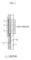
- Fig. 1 is a schematic sectional view of the configuration of the panel of the organic EL display according to the embodiment
- Fig. 2 is a schematic plan view of an organic EL light emitting layer, a main component of the organic EL display according to the embodiment, showing its surface as being enlarged
- Fig. 3 is a schematic plan view of pixels in Fig. 2 as being enlarged.
- Fig. 1 shows a section taken along the line I-I' in Fig. 3 .
- the organic EL display includes a TFT (Thin Film Transistor) element 12 as a switching circuit that controls light emission, for example, on a glass substrate 1 as a transparent substrate.
- the TFT element 12 and the interconnection lines are protected and insulated by a flattening film 10 that forms a flat surface on which an organic EL element is to be stacked.
- a plurality of first electrodes 2 made of a material containing, for example, an indium tin oxide (ITO) alloy as transparent electrodes, a plurality of organic EL layers 3 corresponding to the respective first electrodes 2, and a second electrode 4 made of a material containing aluminum or the like and covering the entire surface are stacked on the flat surface.
- ITO indium tin oxide
- the organic EL layers 3 are held between the associated first electrodes 2 and the second electrode 4, and the fist electrode 2 and the TFT element 12 are connected by a through hole provided at part of the flattening film 10.
- the area of the organic EL layer 3 is formed to be larger than the area of the first electrode 2.
- a plurality of pixels 21 are arranged in a matrix, and the pixels 21 each include a plurality of light emitting regions 11R, 11G, and 11B corresponding to R, G, and B, and a plurality of TFT elements 12 provided corresponding to the light emitting regions and serving as switching circuits that control light emission from the respective light emitting regions.
- the overlapping parts between the first electrodes 2 and the organic EL layers 3 are the light emitting regions 11R, 11G, and 11B.
- the light emitting regions 11R, 11G, and 11B are arranged in a zigzag manner, and non-light emitting regions 13 provided at corners of the light emitting regions prevent adjacent ones among the light emitting regions 11R, 11G, and 11B from contacting each other.
- One pixel 21 is in the shape of a regular square of P ⁇ P.
- the pixels 21 are each divided in two in the vertical direction and three in the horizontal direction into six segments 22a to 22c and 23a to 23c.
- the light emitting regions 11R, 11G, and 11B are provided in the three zigzagged segments 22a to 22c, and the TFT elements 12 are in the remaining three segments 23a to 23c.
- the light emitting regions in the same color are aligned in the vertical direction (Y-direction) with each TFT element 12 interposed therebetween.
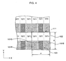
- pixel arrangement in a conventional bottom emission type, active matrix organic EL display is shown in Fig. 4 .
- the light emitting regions 101R, 101G, and 101B constituting the pixel 111 are aligned in the horizontal direction (X-direction), and therefore adjacent light emitting regions are separated by the non-light emitting regions 103 provided at vertical sides of the light emitting regions and the TFT elements 102. Therefore, how much the area of the non-light emitting regions 103 can be reduced is necessarily limited.
- the light emitting regions 11R, 11G, and 11B are provided with notches, in C-chamfer shape in this example (though they may be rounded), as the non-light emitting regions 13 at their respective four corners.
- the non-light emitting regions 13 and the TFT circuits 12 keep adjacent light emitting regions from contacting one another.
- the non-light emitting regions 13 formed at the corners of the light emitting regions occupy only an extremely small area, and the aperture ratio can be improved significantly over that of the example in Fig. 4 .
- a size for a resolution of 160 ppi will be described with reference to Fig. 3 . It is understood that the size is simply by way of example and the invention is not limited thereto.
- the registration margin dm necessary for discrete coloring is 20 ⁇ m ( ⁇ 5 ⁇ m for the registration margin by the pixel film deposition device plus ⁇ 5 ⁇ m for the processing precision for the R, G, and B patterning mask).
- the necessary interconnection lines include a data line 31, a scanning line 32, a power supply line 33, and a storage capacitor line 34, and these lines each have a width in the range of from 5 ⁇ m to 15 ⁇ m.
- the data line 31 is provided in the Y-direction, and the scanning line 32, the power supply line 33, and the storage capacitor line 34 are provided in the X-direction.
- interconnection lines in the TFT element 12 are formed in different layers formed as multiple film layers and connected with each other by a through hole 35 provided in interlayer insulating films. Therefore, a chamfer of C15 ⁇ m provided at the corner of each light emitting region allows the registration margin and the space for the interconnection lines to be secured.
- the segment width of each of the R, G, and B light emitting regions is P/3 relative to the pixel pitch P, and if the registration margin dm for discrete coloring is secured, the width of the light emitting region is P/3 - dm. If the lower limit for the registration margin dm for discrete coloring is applied to design higher resolution arrangement, the ratio of reduction in the width of the light emitting region by dm increases as the pitch P is reduced, and the aperture ratio is reduced.
- the organic EL display according to the embodiment having the above-described configuration was compared to the conventional example (the comparative example described above) regarding the relation between increase in the pixel resolution and the aperture ratio.
- the result is given in Fig. 5 .
- the aperture ratio in the configuration according to the present embodiment is significantly greater than that of the conventional example regardless of the value of the resolution. It has been found that the configuration according to the embodiment considerably, effectively improves the aperture ratio in the bottom emission type, active matrix organic EL panel.
- the present embodiment can improve the aperture ratio by 13.6% over the comparative example. Therefore, according to the embodiment, a display having a bottom emission type, active matrix organic EL panel that efficiently secures a sufficient aperture ratio, has pixel arrangement in which the aperture ratio is hardly a trade off for higher resolution, and can operate with reduced power consumption for obtaining necessary luminance and contribute to downsizing of the driving circuit and the device as a whole can be provided.
- Figs. 6A to 6G are schematic sectional views showing main steps in the process of manufacturing the organic EL display according to the embodiment in the order of the steps.
- the left side on the surface of the sheet corresponds to a section taken along the line II-II' in Fig. 3
- the right side corresponds to a section taken along line III-III' in Fig. 3 .
- a TFT element 12 serving as a switching circuit, and various interconnection lines such as a data line 31, a scanning line 32, a power supply line 33, and a storage capacitor line 34 are formed, and then a flattening film 10 made of a transparent resin is formed to cover them.
- the TFT elements 12 are formed in the parts corresponding to the segments 23a to 23c of the pixel 21 as described above.
- a film of an indium tin oxide (ITO) alloy as a transparent electrode is deposited at the effective light emitting portion described above, and thus first electrodes 2 are formed.
- ITO indium tin oxide
- a vapor deposition mask 5 with an opening 5a corresponding to a region to form a light emitting region is used.
- the vapor deposition mask 5 is placed on the surface of the glass substrate 1 so that the opening 5a is placed only in the position of the organic EL layer 3 corresponding to the light emitting region 11R, and the organic EL layer 3 corresponding to the light emitting region 11R is formed in the segment 22a by vapor deposition.
- the first electrode 2 is completely covered with the organic EL layer 3 for the light emitting region 11R, and the organic EL layer 3 does not overlap the first electrodes 2 for the other colors.
- the mask 5 is moved and placed on the surface of the glass substrate 1 so that the opening 5a is placed only in the position to form an organic EL layer 3 corresponding to the light emitting region 11G and the organic EL layer 3 corresponding to the light emitting region 11G is formed in the segment 22b by vapor deposition.
- the first electrode 2 is completely covered with the organic EL layer 3 for the light emitting region 11G, and the organic EL layer 3 does not overlap the first electrodes 2 for the other colors.
- the mask 5 is moved and placed on the surface of the glass substrate 1 so that the opening 5a is placed only in the position to form the organic EL layer 3 corresponding to the light emitting region 11B and the organic EL layer 3 corresponding to the light emitting region 11B is formed in the segment 22c by vapor deposition.
- the first electrode 2 is completely covered with the organic EL layer 3 for the light emitting region 11B, and the organic EL layer 3 does not overlap the first electrodes 2 for the other colors.
- C-chamfer shaped (or rounded) non-light emitting regions 13 are formed at the four corners of the light emitting regions 11R, 11G, and 11B.
- These non-light emitting regions 13 as well as the segments 23a to 23c for the TFT elements 12 are non-light emitting regions, the organic EL layers 3 are formed so that adjacent light emitting regions are kept from contacting one another in a pixel 21 and a plurality of such pixels 21 are provided in a matrix.
- the organic EL layers 3 corresponding to the light emitting regions 11R, 11G, and 11B are each formed to have an area greater than the corresponding first electrode 2 and cover the same, so that the registration margins for forming the light emitting regions can be secured.
- the TFT element region can be used for securing the registration margin necessary for achieving higher resolution. In this way, the aperture ratio can be improved.
- the light emitting regions for the same colors are aligned with each TFT element 12 interposed therebetween so that the light emitting regions 11R, 11G, and 11B are evenly provided in a plane without contacting one another.
- a vapor deposition mask 6 with openings 6a to expose all the light emitting regions is used and placed on the surface of the glass substrate 1, and an aluminum alloy film is deposited by vapor deposition, thereby forming a second electrode 4 to cover all the light emitting regions.
- a plate 7 made of glass or the like that prevents moisture penetration is adhesively fixed, for example, with an adhesive 8 to cover the second electrode 4, so that the organic EL layers 3 are prevented from deteriorating by moisture and the like.
- Various conductive members formed on the glass substrate 1 are connected to a driving circuit (not shown) through the interconnection line 9 of an FPC (Flexible Printed Circuit).
- a bottom emission type, active matrix organic EL display for example, with a resolution of 160 ppi and an aperture ratio of 44.7% is produced.
- the single vapor deposition mask 5 can readily be formed using a single film deposition chamber, low molecular organic EL can be deposited by vapor deposition, and an organic EL display having the above-described configuration can readily be provided with reliability.
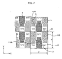
- Fig. 7 is a schematic plan view of an organic EL light emitting layer, a main part of an organic EL display according to Modification 1, showing its surface as being enlarged.
- the areas of the light emitting regions 11R, 11G, and 11B in the pixel 21 are each greater than the area of the TFT element 12.
- the registration margins necessary for discrete coloring into the three colors can be included in the segments of the TFT elements 12, so that the aperture ratio can be increased.
- Fig. 8 is a schematic plan view of an organic EL light emitting layer, a main part of an organic EL display according to Modification 2, showing its surface as being enlarged.
- the areas of the light emitting regions 11R, 11G, and 11B in the pixel 21 are each smaller than the area of the TFT element 12.
- adjacent TFT elements 12 separate adjacent light emitting regions, and therefore there is no necessity for providing non-light emitting regions in association with the light emitting regions, so that the aperture ratio can be increased (in the shown example, the segments for the TFT elements 12 are in contact with each other).
- a display device having a bottom emission type, active matrix organic EL panel that efficiently secures a sufficient aperture ratio, has pixel arrangement in which the aperture ratio is hardly a trade off for higher resolution, and can operate with reduced power consumption for obtaining necessary luminance and contribute to downsizing of the driving circuit and the device as a whole, and a manufacturing method that allows the configuration of such a device to be readily provided can be provided with reliability.
Abstract
Claims (13)
- Dispositif d'affichage comportant un panneau électroluminescent organique à matrice active comprenant :des première et deuxième électrodes prévues sur un substrat, etune couche d'émission de lumière électroluminescente organique prévue entre lesdites première et deuxième électrodes, dans lequelladite couche d'émission de lumière électroluminescente organique comprend des régions d'émission de lumière, agencées en zigzag, et les régions adjacentes parmi lesdites régions d'émission de lumière sont empêchées de venir en contact les unes avec les autres, dans lequel,trois types desdites régions d'émission de lumière correspondant à R, G et B et trois circuits de commutation correspondant aux trois types desdites régions d'émission de lumière sont agencés en une matrice, etdans six segments agencés en deux rangées et trois colonnes, lesdites régions d'émission de lumière sont agencées dans trois desdits segments positionnés en zigzag et lesdits trois circuits de commutation sont agencés dans les trois segments restants.
- Dispositif d'affichage selon la revendication 1, dans lequel
lesdites régions d'émission de lumière pour la même couleur sont alignées avec ledit circuit de commutation interposé entre elles. - Dispositif d'affichage selon la revendication 1, dans lequel
l'aire de ladite couche d'émission de lumière électroluminescente organique est plus grande que l'aire de ladite première électrode. - Dispositif d'affichage selon la revendication 1, dans lequel
une région de non émission de lumière est formée au niveau d'un coin de ladite région d'émission de lumière, et les régions adjacentes parmi lesdites régions d'émission de lumière sont séparées par ladite région de non émission de lumière. - Dispositif d'affichage selon la revendication 1, dans lequel
l'aire de ladite région d'émission de lumière est plus grande que l'aire dudit circuit de commutation. - Dispositif d'affichage selon la revendication 1, dans lequel
ladite région d'émission de lumière a une aire plus petite que l'aire dudit circuit de commutation et est séparée de la région adjacente parmi lesdites régions d'émission de lumière avec ledit circuit de commutation interposé entre elles. - Procédé de fabrication d'un dispositif d'affichage comportant un panneau électroluminescent organique à matrice active comprenant des première et deuxième électrodes prévues sur un substrat et une couche d'émission de lumière électroluminescente organique prévue entre lesdites première et deuxième électrodes, dans lequel ladite couche d'émission de lumière électroluminescente organique comprend une région d'émission de lumière, le procédé comprenant l'étape consistant à
former une pluralité desdites régions d'émission de lumière par dépôt d'un masque en phase vapeur, dans lequel lesdites couches d'émission de lumière électroluminescentes organiques correspondant à chacune desdites régions d'émission de lumière sont agencées en zigzag et les régions adjacentes parmi lesdites régions d'émission de lumière sont empêchées de venir en contact les unes avec les autres, dans lequel :trois types desdites régions d'émission de lumière correspondant à R, G et B et lesdits trois circuits de commutation correspondant aux trois types desdites régions d'émission de lumière sont agencés en une matrice ;dans six segments agencés en deux rangées et trois colonnes, lesdites régions d'émission de lumière sont agencées dans trois desdits segments positionnés en zigzag et lesdits trois circuits de commutation sont agencés dans les trois segments restants. - Procédé de fabrication d'un dispositif d'affichage selon la revendication 7, dans lequel
le même masque est déplacé séquentiellement pour former lesdites couches d'émission de lumière électroluminescentes organiques correspondant à chacune desdites régions d'émission de lumière. - Procédé de fabrication d'un dispositif d'affichage selon la revendication 7, dans lequel
lesdites régions d'émission de lumière pour la même couleur sont alignées avec ledit circuit de commutation interposé entre elles. - Procédé de fabrication d'un dispositif d'affichage selon la revendication 7, dans lequel
ladite couche d'émission de lumière électroluminescente organique est formée de manière à avoir une aire plus grande que l'aire de ladite première électrode. - Procédé de fabrication d'un dispositif d'affichage selon la revendication 7, dans lequel
ladite région d'émission de lumière est formée de manière à avoir une partie de coin servant en tant que région de non émission de lumière. - Procédé de fabrication d'un dispositif d'affichage selon la revendication 7, dans lequel
ladite région d'émission de lumière est formée de manière à avoir une aire plus grande que l'aire dudit circuit de commutation. - Procédé de fabrication d'un dispositif d'affichage selon la revendication 7, dans lequel
ladite région d'émission de lumière a une aire plus petite que l'aire dudit circuit de commutation et est séparée de la région adjacente parmi lesdites régions d'émission de lumière avec ledit circuit de commutation interposé entre elles.
Applications Claiming Priority (1)
| Application Number | Priority Date | Filing Date | Title |
|---|---|---|---|
| PCT/JP2003/001464 WO2004073356A1 (fr) | 2003-02-13 | 2003-02-13 | Appareil d'affichage et procede de fabrication correspondant |
Publications (3)
| Publication Number | Publication Date |
|---|---|
| EP1594347A1 EP1594347A1 (fr) | 2005-11-09 |
| EP1594347A4 EP1594347A4 (fr) | 2008-03-19 |
| EP1594347B1 true EP1594347B1 (fr) | 2010-12-08 |
Family
ID=32866106
Family Applications (1)
| Application Number | Title | Priority Date | Filing Date |
|---|---|---|---|
| EP03705089A Expired - Lifetime EP1594347B1 (fr) | 2003-02-13 | 2003-02-13 | Appareil d'affichage et procede de fabrication correspondant |
Country Status (5)
| Country | Link |
|---|---|
| US (1) | US7368868B2 (fr) |
| EP (1) | EP1594347B1 (fr) |
| JP (1) | JP4287820B2 (fr) |
| DE (1) | DE60335300D1 (fr) |
| WO (1) | WO2004073356A1 (fr) |
Cited By (27)
| Publication number | Priority date | Publication date | Assignee | Title |
|---|---|---|---|---|
| US8599191B2 (en) | 2011-05-20 | 2013-12-03 | Ignis Innovation Inc. | System and methods for extraction of threshold and mobility parameters in AMOLED displays |
| US8743096B2 (en) | 2006-04-19 | 2014-06-03 | Ignis Innovation, Inc. | Stable driving scheme for active matrix displays |
| US8803417B2 (en) | 2009-12-01 | 2014-08-12 | Ignis Innovation Inc. | High resolution pixel architecture |
| US8816946B2 (en) | 2004-12-15 | 2014-08-26 | Ignis Innovation Inc. | Method and system for programming, calibrating and driving a light emitting device display |
| US8907991B2 (en) | 2010-12-02 | 2014-12-09 | Ignis Innovation Inc. | System and methods for thermal compensation in AMOLED displays |
| USRE45291E1 (en) | 2004-06-29 | 2014-12-16 | Ignis Innovation Inc. | Voltage-programming scheme for current-driven AMOLED displays |
| US8922544B2 (en) | 2012-05-23 | 2014-12-30 | Ignis Innovation Inc. | Display systems with compensation for line propagation delay |
| US8941697B2 (en) | 2003-09-23 | 2015-01-27 | Ignis Innovation Inc. | Circuit and method for driving an array of light emitting pixels |
| US8994617B2 (en) | 2010-03-17 | 2015-03-31 | Ignis Innovation Inc. | Lifetime uniformity parameter extraction methods |
| US9093028B2 (en) | 2009-12-06 | 2015-07-28 | Ignis Innovation Inc. | System and methods for power conservation for AMOLED pixel drivers |
| US9093029B2 (en) | 2011-05-20 | 2015-07-28 | Ignis Innovation Inc. | System and methods for extraction of threshold and mobility parameters in AMOLED displays |
| US9111485B2 (en) | 2009-06-16 | 2015-08-18 | Ignis Innovation Inc. | Compensation technique for color shift in displays |
| US9125278B2 (en) | 2006-08-15 | 2015-09-01 | Ignis Innovation Inc. | OLED luminance degradation compensation |
| US9171500B2 (en) | 2011-05-20 | 2015-10-27 | Ignis Innovation Inc. | System and methods for extraction of parasitic parameters in AMOLED displays |
| US9171504B2 (en) | 2013-01-14 | 2015-10-27 | Ignis Innovation Inc. | Driving scheme for emissive displays providing compensation for driving transistor variations |
| US9275579B2 (en) | 2004-12-15 | 2016-03-01 | Ignis Innovation Inc. | System and methods for extraction of threshold and mobility parameters in AMOLED displays |
| US9280933B2 (en) | 2004-12-15 | 2016-03-08 | Ignis Innovation Inc. | System and methods for extraction of threshold and mobility parameters in AMOLED displays |
| US9305488B2 (en) | 2013-03-14 | 2016-04-05 | Ignis Innovation Inc. | Re-interpolation with edge detection for extracting an aging pattern for AMOLED displays |
| US9311859B2 (en) | 2009-11-30 | 2016-04-12 | Ignis Innovation Inc. | Resetting cycle for aging compensation in AMOLED displays |
| US9324268B2 (en) | 2013-03-15 | 2016-04-26 | Ignis Innovation Inc. | Amoled displays with multiple readout circuits |
| US9336717B2 (en) | 2012-12-11 | 2016-05-10 | Ignis Innovation Inc. | Pixel circuits for AMOLED displays |
| US9343006B2 (en) | 2012-02-03 | 2016-05-17 | Ignis Innovation Inc. | Driving system for active-matrix displays |
| US9384698B2 (en) | 2009-11-30 | 2016-07-05 | Ignis Innovation Inc. | System and methods for aging compensation in AMOLED displays |
| US9430958B2 (en) | 2010-02-04 | 2016-08-30 | Ignis Innovation Inc. | System and methods for extracting correlation curves for an organic light emitting device |
| US9437137B2 (en) | 2013-08-12 | 2016-09-06 | Ignis Innovation Inc. | Compensation accuracy |
| US9466240B2 (en) | 2011-05-26 | 2016-10-11 | Ignis Innovation Inc. | Adaptive feedback system for compensating for aging pixel areas with enhanced estimation speed |
| US9530349B2 (en) | 2011-05-20 | 2016-12-27 | Ignis Innovations Inc. | Charged-based compensation and parameter extraction in AMOLED displays |
Families Citing this family (63)
| Publication number | Priority date | Publication date | Assignee | Title |
|---|---|---|---|---|
| US7483001B2 (en) | 2001-11-21 | 2009-01-27 | Seiko Epson Corporation | Active matrix substrate, electro-optical device, and electronic device |
| US10013907B2 (en) | 2004-12-15 | 2018-07-03 | Ignis Innovation Inc. | Method and system for programming, calibrating and/or compensating, and driving an LED display |
| US20140111567A1 (en) | 2005-04-12 | 2014-04-24 | Ignis Innovation Inc. | System and method for compensation of non-uniformities in light emitting device displays |
| US10012678B2 (en) | 2004-12-15 | 2018-07-03 | Ignis Innovation Inc. | Method and system for programming, calibrating and/or compensating, and driving an LED display |
| US9799246B2 (en) | 2011-05-20 | 2017-10-24 | Ignis Innovation Inc. | System and methods for extraction of threshold and mobility parameters in AMOLED displays |
| JP2006181980A (ja) * | 2004-12-28 | 2006-07-13 | Seiko Epson Corp | 露光ヘッド及び画像形成装置 |
| US7612368B2 (en) * | 2004-12-29 | 2009-11-03 | E.I. Du Pont De Nemours And Company | Organic bottom emission electronic device |
| CA2496642A1 (fr) | 2005-02-10 | 2006-08-10 | Ignis Innovation Inc. | Methode d'attaque a courte duree de stabilisation pour afficheurs a diodes organiques electroluminescentes (oled) programmes par courant |
| US8866707B2 (en) * | 2005-03-31 | 2014-10-21 | Semiconductor Energy Laboratory Co., Ltd. | Display device, and apparatus using the display device having a polygonal pixel electrode |
| JP5177957B2 (ja) * | 2005-03-31 | 2013-04-10 | 株式会社半導体エネルギー研究所 | 表示装置、およびそれを用いた電子機器 |
| KR101219036B1 (ko) | 2005-05-02 | 2013-01-07 | 삼성디스플레이 주식회사 | 유기 발광 표시 장치 |
| KR100683403B1 (ko) * | 2005-05-31 | 2007-02-15 | 엘지.필립스 엘시디 주식회사 | 유기전계발광소자 및 그 제조 방법 |
| CN102663977B (zh) | 2005-06-08 | 2015-11-18 | 伊格尼斯创新有限公司 | 用于驱动发光器件显示器的方法和系统 |
| JP5613360B2 (ja) * | 2005-07-04 | 2014-10-22 | 株式会社半導体エネルギー研究所 | 表示装置、表示モジュール及び電子機器 |
| US7898623B2 (en) | 2005-07-04 | 2011-03-01 | Semiconductor Energy Laboratory Co., Ltd. | Display device, electronic device and method of driving display device |
| CA2518276A1 (fr) | 2005-09-13 | 2007-03-13 | Ignis Innovation Inc. | Technique de compensation de la degradation de luminance dans des dispositifs electroluminescents |
| KR101293568B1 (ko) * | 2006-02-23 | 2013-08-06 | 삼성디스플레이 주식회사 | 표시 장치 |
| US20080001525A1 (en) * | 2006-06-30 | 2008-01-03 | Au Optronics Corporation | Arrangements of color pixels for full color OLED |
| JP4623114B2 (ja) * | 2008-03-23 | 2011-02-02 | ソニー株式会社 | El表示パネル及び電子機器 |
| JP4623138B2 (ja) | 2008-05-21 | 2011-02-02 | ソニー株式会社 | 表示装置および電子機器 |
| JP5176993B2 (ja) * | 2009-02-02 | 2013-04-03 | セイコーエプソン株式会社 | 電気光学装置及び電子機器 |
| US8896505B2 (en) | 2009-06-12 | 2014-11-25 | Global Oled Technology Llc | Display with pixel arrangement |
| CA2688870A1 (fr) | 2009-11-30 | 2011-05-30 | Ignis Innovation Inc. | Procede et techniques pour ameliorer l'uniformite d'affichage |
| US10319307B2 (en) | 2009-06-16 | 2019-06-11 | Ignis Innovation Inc. | Display system with compensation techniques and/or shared level resources |
| US10996258B2 (en) | 2009-11-30 | 2021-05-04 | Ignis Innovation Inc. | Defect detection and correction of pixel circuits for AMOLED displays |
| CA2686174A1 (fr) * | 2009-12-01 | 2011-06-01 | Ignis Innovation Inc | Architecture de pixels haute resolution |
| US10176736B2 (en) | 2010-02-04 | 2019-01-08 | Ignis Innovation Inc. | System and methods for extracting correlation curves for an organic light emitting device |
| US9881532B2 (en) | 2010-02-04 | 2018-01-30 | Ignis Innovation Inc. | System and method for extracting correlation curves for an organic light emitting device |
| US20140313111A1 (en) | 2010-02-04 | 2014-10-23 | Ignis Innovation Inc. | System and methods for extracting correlation curves for an organic light emitting device |
| US10089921B2 (en) | 2010-02-04 | 2018-10-02 | Ignis Innovation Inc. | System and methods for extracting correlation curves for an organic light emitting device |
| US10163401B2 (en) | 2010-02-04 | 2018-12-25 | Ignis Innovation Inc. | System and methods for extracting correlation curves for an organic light emitting device |
| KR101257734B1 (ko) * | 2010-09-08 | 2013-04-24 | 엘지디스플레이 주식회사 | 유기전계발광 표시장치 |
| WO2012164475A2 (fr) | 2011-05-27 | 2012-12-06 | Ignis Innovation Inc. | Systèmes et procédés de compensation du vieillissement dans des écrans amoled |
| US10089924B2 (en) | 2011-11-29 | 2018-10-02 | Ignis Innovation Inc. | Structural and low-frequency non-uniformity compensation |
| KR101615332B1 (ko) | 2012-03-06 | 2016-04-26 | 삼성디스플레이 주식회사 | 유기 발광 표시 장치의 화소 배열 구조 |
| KR102061283B1 (ko) * | 2012-09-13 | 2020-01-02 | 삼성디스플레이 주식회사 | 유기 발광 표시 장치의 화소 배열 구조 |
| US10832616B2 (en) | 2012-03-06 | 2020-11-10 | Samsung Display Co., Ltd. | Pixel arrangement structure for organic light emitting diode display |
| US9190456B2 (en) | 2012-04-25 | 2015-11-17 | Ignis Innovation Inc. | High resolution display panel with emissive organic layers emitting light of different colors |
| US9747834B2 (en) | 2012-05-11 | 2017-08-29 | Ignis Innovation Inc. | Pixel circuits including feedback capacitors and reset capacitors, and display systems therefore |
| EP2709155B1 (fr) * | 2012-09-13 | 2020-11-11 | Samsung Display Co., Ltd. | Structure de disposition de pixels pour dispositif d'affichage à diodes électroluminescentes organiques |
| US9786223B2 (en) | 2012-12-11 | 2017-10-10 | Ignis Innovation Inc. | Pixel circuits for AMOLED displays |
| US9830857B2 (en) | 2013-01-14 | 2017-11-28 | Ignis Innovation Inc. | Cleaning common unwanted signals from pixel measurements in emissive displays |
| WO2014174427A1 (fr) | 2013-04-22 | 2014-10-30 | Ignis Innovation Inc. | Système d'inspection pour panneaux d'affichage panneaux d'affichage à diodes électroluminescentes organiques |
| KR101427593B1 (ko) | 2013-04-26 | 2014-08-07 | 삼성디스플레이 주식회사 | 유기 발광 표시 장치 |
| US9741282B2 (en) | 2013-12-06 | 2017-08-22 | Ignis Innovation Inc. | OLED display system and method |
| US9761170B2 (en) | 2013-12-06 | 2017-09-12 | Ignis Innovation Inc. | Correction for localized phenomena in an image array |
| US9502653B2 (en) | 2013-12-25 | 2016-11-22 | Ignis Innovation Inc. | Electrode contacts |
| CN104009066B (zh) * | 2013-12-31 | 2018-03-02 | 昆山工研院新型平板显示技术中心有限公司 | 一种像素结构及采用该像素结构的有机发光显示器 |
| CN104752469B (zh) * | 2013-12-31 | 2018-08-03 | 昆山国显光电有限公司 | 一种像素结构及采用该像素结构的有机发光显示器 |
| CN104037197B (zh) * | 2013-12-31 | 2017-06-16 | 昆山国显光电有限公司 | 一种像素结构及采用该像素结构的有机发光显示器 |
| CN103898441A (zh) * | 2014-03-13 | 2014-07-02 | 昆山允升吉光电科技有限公司 | 一种配套掩模板及其蒸镀方法 |
| CN103898442A (zh) * | 2014-03-13 | 2014-07-02 | 昆山允升吉光电科技有限公司 | 一种配套掩模板及其蒸镀方法 |
| CN103904105A (zh) * | 2014-03-13 | 2014-07-02 | 昆山允升吉光电科技有限公司 | 一种oled显示屏的像素结构 |
| US10192479B2 (en) | 2014-04-08 | 2019-01-29 | Ignis Innovation Inc. | Display system using system level resources to calculate compensation parameters for a display module in a portable device |
| KR102184784B1 (ko) * | 2014-06-30 | 2020-11-30 | 엘지디스플레이 주식회사 | 투명 유기 발광 표시 장치 |
| CA2879462A1 (fr) | 2015-01-23 | 2016-07-23 | Ignis Innovation Inc. | Compensation de la variation de couleur dans les dispositifs emetteurs |
| CA2889870A1 (fr) | 2015-05-04 | 2016-11-04 | Ignis Innovation Inc. | Systeme de retroaction optique |
| CA2892714A1 (fr) | 2015-05-27 | 2016-11-27 | Ignis Innovation Inc | Reduction de largeur de bande de memoire dans un systeme de compensation |
| CA2900170A1 (fr) | 2015-08-07 | 2017-02-07 | Gholamreza Chaji | Etalonnage de pixel fonde sur des valeurs de reference ameliorees |
| KR102446205B1 (ko) * | 2015-11-18 | 2022-09-23 | 삼성디스플레이 주식회사 | 표시 장치 |
| US10394091B2 (en) * | 2015-11-18 | 2019-08-27 | Samsung Display Co., Ltd. | Liquid crystal display device |
| KR102602169B1 (ko) * | 2016-07-11 | 2023-11-14 | 삼성디스플레이 주식회사 | 표시 장치 |
| KR20210038224A (ko) * | 2019-09-30 | 2021-04-07 | 엘지디스플레이 주식회사 | 표시 장치 |
Family Cites Families (13)
| Publication number | Priority date | Publication date | Assignee | Title |
|---|---|---|---|---|
| JPS60218626A (ja) * | 1984-04-13 | 1985-11-01 | Sharp Corp | カラ−液晶表示装置 |
| WO1999020080A1 (fr) * | 1997-10-15 | 1999-04-22 | Toray Industries, Inc. | Procede de fabrication d'un dispositif electroluminescent organique |
| JP3879281B2 (ja) | 1998-11-06 | 2007-02-07 | カシオ計算機株式会社 | 表示装置及び表示装置の駆動方法 |
| JP2000228284A (ja) * | 1998-12-01 | 2000-08-15 | Sanyo Electric Co Ltd | カラーel表示装置 |
| JP2000227770A (ja) * | 1998-12-01 | 2000-08-15 | Sanyo Electric Co Ltd | カラーel表示装置 |
| JP2000214800A (ja) | 1999-01-20 | 2000-08-04 | Sanyo Electric Co Ltd | エレクトロルミネッセンス表示装置 |
| JP2001085162A (ja) * | 1999-09-10 | 2001-03-30 | Sharp Corp | 有機発光素子及びその製造方法 |
| JP4497596B2 (ja) * | 1999-09-30 | 2010-07-07 | 三洋電機株式会社 | 薄膜トランジスタ及び表示装置 |
| JP2002056972A (ja) | 2000-08-08 | 2002-02-22 | Sharp Corp | 有機発光素子の製造方法および有機発光素子 |
| JP4925528B2 (ja) * | 2000-09-29 | 2012-04-25 | 三洋電機株式会社 | 表示装置 |
| JP3620490B2 (ja) * | 2000-11-22 | 2005-02-16 | ソニー株式会社 | アクティブマトリクス型表示装置 |
| JP2002215063A (ja) * | 2001-01-19 | 2002-07-31 | Sony Corp | アクティブマトリクス型表示装置 |
| KR100741967B1 (ko) * | 2004-11-08 | 2007-07-23 | 삼성에스디아이 주식회사 | 평판표시장치 |
-
2003
- 2003-02-13 WO PCT/JP2003/001464 patent/WO2004073356A1/fr active Application Filing
- 2003-02-13 EP EP03705089A patent/EP1594347B1/fr not_active Expired - Lifetime
- 2003-02-13 JP JP2004568176A patent/JP4287820B2/ja not_active Expired - Lifetime
- 2003-02-13 DE DE60335300T patent/DE60335300D1/de not_active Expired - Lifetime
-
2005
- 2005-03-18 US US11/083,025 patent/US7368868B2/en not_active Expired - Lifetime
Cited By (40)
| Publication number | Priority date | Publication date | Assignee | Title |
|---|---|---|---|---|
| US9472139B2 (en) | 2003-09-23 | 2016-10-18 | Ignis Innovation Inc. | Circuit and method for driving an array of light emitting pixels |
| US9472138B2 (en) | 2003-09-23 | 2016-10-18 | Ignis Innovation Inc. | Pixel driver circuit with load-balance in current mirror circuit |
| US8941697B2 (en) | 2003-09-23 | 2015-01-27 | Ignis Innovation Inc. | Circuit and method for driving an array of light emitting pixels |
| USRE45291E1 (en) | 2004-06-29 | 2014-12-16 | Ignis Innovation Inc. | Voltage-programming scheme for current-driven AMOLED displays |
| US8816946B2 (en) | 2004-12-15 | 2014-08-26 | Ignis Innovation Inc. | Method and system for programming, calibrating and driving a light emitting device display |
| US9280933B2 (en) | 2004-12-15 | 2016-03-08 | Ignis Innovation Inc. | System and methods for extraction of threshold and mobility parameters in AMOLED displays |
| US9275579B2 (en) | 2004-12-15 | 2016-03-01 | Ignis Innovation Inc. | System and methods for extraction of threshold and mobility parameters in AMOLED displays |
| US8994625B2 (en) | 2004-12-15 | 2015-03-31 | Ignis Innovation Inc. | Method and system for programming, calibrating and driving a light emitting device display |
| US8743096B2 (en) | 2006-04-19 | 2014-06-03 | Ignis Innovation, Inc. | Stable driving scheme for active matrix displays |
| US9530352B2 (en) | 2006-08-15 | 2016-12-27 | Ignis Innovations Inc. | OLED luminance degradation compensation |
| US9125278B2 (en) | 2006-08-15 | 2015-09-01 | Ignis Innovation Inc. | OLED luminance degradation compensation |
| US9111485B2 (en) | 2009-06-16 | 2015-08-18 | Ignis Innovation Inc. | Compensation technique for color shift in displays |
| US9117400B2 (en) | 2009-06-16 | 2015-08-25 | Ignis Innovation Inc. | Compensation technique for color shift in displays |
| US9418587B2 (en) | 2009-06-16 | 2016-08-16 | Ignis Innovation Inc. | Compensation technique for color shift in displays |
| US9311859B2 (en) | 2009-11-30 | 2016-04-12 | Ignis Innovation Inc. | Resetting cycle for aging compensation in AMOLED displays |
| US9384698B2 (en) | 2009-11-30 | 2016-07-05 | Ignis Innovation Inc. | System and methods for aging compensation in AMOLED displays |
| US8803417B2 (en) | 2009-12-01 | 2014-08-12 | Ignis Innovation Inc. | High resolution pixel architecture |
| US9093028B2 (en) | 2009-12-06 | 2015-07-28 | Ignis Innovation Inc. | System and methods for power conservation for AMOLED pixel drivers |
| US9262965B2 (en) | 2009-12-06 | 2016-02-16 | Ignis Innovation Inc. | System and methods for power conservation for AMOLED pixel drivers |
| US9430958B2 (en) | 2010-02-04 | 2016-08-30 | Ignis Innovation Inc. | System and methods for extracting correlation curves for an organic light emitting device |
| US8994617B2 (en) | 2010-03-17 | 2015-03-31 | Ignis Innovation Inc. | Lifetime uniformity parameter extraction methods |
| US8907991B2 (en) | 2010-12-02 | 2014-12-09 | Ignis Innovation Inc. | System and methods for thermal compensation in AMOLED displays |
| US9489897B2 (en) | 2010-12-02 | 2016-11-08 | Ignis Innovation Inc. | System and methods for thermal compensation in AMOLED displays |
| US9589490B2 (en) | 2011-05-20 | 2017-03-07 | Ignis Innovation Inc. | System and methods for extraction of threshold and mobility parameters in AMOLED displays |
| US8599191B2 (en) | 2011-05-20 | 2013-12-03 | Ignis Innovation Inc. | System and methods for extraction of threshold and mobility parameters in AMOLED displays |
| US9355584B2 (en) | 2011-05-20 | 2016-05-31 | Ignis Innovation Inc. | System and methods for extraction of threshold and mobility parameters in AMOLED displays |
| US9530349B2 (en) | 2011-05-20 | 2016-12-27 | Ignis Innovations Inc. | Charged-based compensation and parameter extraction in AMOLED displays |
| US9093029B2 (en) | 2011-05-20 | 2015-07-28 | Ignis Innovation Inc. | System and methods for extraction of threshold and mobility parameters in AMOLED displays |
| US9171500B2 (en) | 2011-05-20 | 2015-10-27 | Ignis Innovation Inc. | System and methods for extraction of parasitic parameters in AMOLED displays |
| US9466240B2 (en) | 2011-05-26 | 2016-10-11 | Ignis Innovation Inc. | Adaptive feedback system for compensating for aging pixel areas with enhanced estimation speed |
| US9343006B2 (en) | 2012-02-03 | 2016-05-17 | Ignis Innovation Inc. | Driving system for active-matrix displays |
| US9536460B2 (en) | 2012-05-23 | 2017-01-03 | Ignis Innovation Inc. | Display systems with compensation for line propagation delay |
| US9368063B2 (en) | 2012-05-23 | 2016-06-14 | Ignis Innovation Inc. | Display systems with compensation for line propagation delay |
| US8922544B2 (en) | 2012-05-23 | 2014-12-30 | Ignis Innovation Inc. | Display systems with compensation for line propagation delay |
| US9336717B2 (en) | 2012-12-11 | 2016-05-10 | Ignis Innovation Inc. | Pixel circuits for AMOLED displays |
| US9171504B2 (en) | 2013-01-14 | 2015-10-27 | Ignis Innovation Inc. | Driving scheme for emissive displays providing compensation for driving transistor variations |
| US9305488B2 (en) | 2013-03-14 | 2016-04-05 | Ignis Innovation Inc. | Re-interpolation with edge detection for extracting an aging pattern for AMOLED displays |
| US9536465B2 (en) | 2013-03-14 | 2017-01-03 | Ignis Innovation Inc. | Re-interpolation with edge detection for extracting an aging pattern for AMOLED displays |
| US9324268B2 (en) | 2013-03-15 | 2016-04-26 | Ignis Innovation Inc. | Amoled displays with multiple readout circuits |
| US9437137B2 (en) | 2013-08-12 | 2016-09-06 | Ignis Innovation Inc. | Compensation accuracy |
Also Published As
| Publication number | Publication date |
|---|---|
| EP1594347A4 (fr) | 2008-03-19 |
| JP4287820B2 (ja) | 2009-07-01 |
| US7368868B2 (en) | 2008-05-06 |
| JPWO2004073356A1 (ja) | 2006-06-01 |
| WO2004073356A1 (fr) | 2004-08-26 |
| US20050162079A1 (en) | 2005-07-28 |
| EP1594347A1 (fr) | 2005-11-09 |
| DE60335300D1 (de) | 2011-01-20 |
Similar Documents
| Publication | Publication Date | Title |
|---|---|---|
| EP1594347B1 (fr) | Appareil d'affichage et procede de fabrication correspondant | |
| US11910683B2 (en) | Display panel and display device | |
| EP3333895B1 (fr) | Afficheur électroluminescent organique | |
| KR101695082B1 (ko) | 표시장치 | |
| US5742129A (en) | Organic electroluminescent display panel with projecting ramparts and method for manufacturing the same | |
| CN101764144B (zh) | El装置、el装置的制造方法及电子设备 | |
| CN111584591A (zh) | 显示面板、驱动方法及显示装置 | |
| US20170250367A1 (en) | Display device | |
| US20220077276A1 (en) | Electronic device, display apparatus, display substrate and manufacturing method therefor | |
| CN115224091A (zh) | 一种显示面板及显示装置 | |
| KR102572407B1 (ko) | 박막 트랜지스터 어레이 기판 및 이를 포함하는 유기발광 표시장치 | |
| JP7048292B2 (ja) | 有機el表示装置 | |
| US20050046341A1 (en) | OLED display and method for manufacturing thereof | |
| US20220181429A1 (en) | Display device | |
| CN108364991B (zh) | 有机发光二极管显示基板及其制备方法、显示装置 | |
| JP2011526719A (ja) | 発光装置 | |
| CN100336095C (zh) | 主动矩阵型显示装置 | |
| US11818930B2 (en) | Display device | |
| JP7344004B2 (ja) | Oled表示装置及びoled表示装置の製造方法 | |
| JP4639662B2 (ja) | 電気光学装置および電子機器 | |
| JP2006317740A (ja) | 発光装置、その駆動方法および製造方法、ならびに電子機器 | |
| US20220199937A1 (en) | Display device | |
| CN114725163A (zh) | 显示装置 | |
| CN114335081A (zh) | 显示面板和显示设备 | |
| KR100713048B1 (ko) | 표시 장치 및 그 제조 방법 |
Legal Events
| Date | Code | Title | Description |
|---|---|---|---|
| PUAI | Public reference made under article 153(3) epc to a published international application that has entered the european phase |
Free format text: ORIGINAL CODE: 0009012 |
|
| 17P | Request for examination filed |
Effective date: 20050331 |
|
| AK | Designated contracting states |
Kind code of ref document: A1 Designated state(s): AT BE BG CH CY CZ DE DK EE ES FI FR GB GR HU IE IT LI LU MC NL PT SE SI SK TR |
|
| RBV | Designated contracting states (corrected) |
Designated state(s): DE FR GB |
|
| RAP1 | Party data changed (applicant data changed or rights of an application transferred) |
Owner name: FUJI PHOTO FILM CO., LTD. |
|
| RAP1 | Party data changed (applicant data changed or rights of an application transferred) |
Owner name: FUJIFILM CORPORATION |
|
| A4 | Supplementary search report drawn up and despatched |
Effective date: 20080218 |
|
| 17Q | First examination report despatched |
Effective date: 20080901 |
|
| RIC1 | Information provided on ipc code assigned before grant |
Ipc: H01L 27/32 20060101AFI20100422BHEP |
|
| GRAP | Despatch of communication of intention to grant a patent |
Free format text: ORIGINAL CODE: EPIDOSNIGR1 |
|
| GRAS | Grant fee paid |
Free format text: ORIGINAL CODE: EPIDOSNIGR3 |
|
| GRAA | (expected) grant |
Free format text: ORIGINAL CODE: 0009210 |
|
| AK | Designated contracting states |
Kind code of ref document: B1 Designated state(s): DE FR GB |
|
| REG | Reference to a national code |
Ref country code: GB Ref legal event code: FG4D |
|
| REF | Corresponds to: |
Ref document number: 60335300 Country of ref document: DE Date of ref document: 20110120 Kind code of ref document: P |
|
| PLBE | No opposition filed within time limit |
Free format text: ORIGINAL CODE: 0009261 |
|
| STAA | Information on the status of an ep patent application or granted ep patent |
Free format text: STATUS: NO OPPOSITION FILED WITHIN TIME LIMIT |
|
| 26N | No opposition filed |
Effective date: 20110909 |
|
| REG | Reference to a national code |
Ref country code: DE Ref legal event code: R097 Ref document number: 60335300 Country of ref document: DE Effective date: 20110909 |
|
| REG | Reference to a national code |
Ref country code: DE Ref legal event code: R082 Ref document number: 60335300 Country of ref document: DE Representative=s name: HOFFMANN - EITLE, DE |
|
| REG | Reference to a national code |
Ref country code: GB Ref legal event code: 732E Free format text: REGISTERED BETWEEN 20121025 AND 20121031 |
|
| REG | Reference to a national code |
Ref country code: DE Ref legal event code: R081 Ref document number: 60335300 Country of ref document: DE Owner name: UDC IRELAND LTD., IE Free format text: FORMER OWNER: FUJIFILM CORP., TOKIO/TOKYO, JP Effective date: 20121002 Ref country code: DE Ref legal event code: R082 Ref document number: 60335300 Country of ref document: DE Representative=s name: HOFFMANN - EITLE, DE Effective date: 20121002 Ref country code: DE Ref legal event code: R082 Ref document number: 60335300 Country of ref document: DE Representative=s name: HOFFMANN - EITLE PATENT- UND RECHTSANWAELTE PA, DE Effective date: 20121002 |
|
| REG | Reference to a national code |
Ref country code: FR Ref legal event code: PLFP Year of fee payment: 14 |
|
| REG | Reference to a national code |
Ref country code: FR Ref legal event code: PLFP Year of fee payment: 15 |
|
| REG | Reference to a national code |
Ref country code: FR Ref legal event code: PLFP Year of fee payment: 16 |
|
| PGFP | Annual fee paid to national office [announced via postgrant information from national office to epo] |
Ref country code: FR Payment date: 20211217 Year of fee payment: 20 Ref country code: GB Payment date: 20211223 Year of fee payment: 20 |
|
| PGFP | Annual fee paid to national office [announced via postgrant information from national office to epo] |
Ref country code: DE Payment date: 20211222 Year of fee payment: 20 |
|
| REG | Reference to a national code |
Ref country code: DE Ref legal event code: R071 Ref document number: 60335300 Country of ref document: DE |
|
| REG | Reference to a national code |
Ref country code: GB Ref legal event code: PE20 Expiry date: 20230212 |
|
| PG25 | Lapsed in a contracting state [announced via postgrant information from national office to epo] |
Ref country code: GB Free format text: LAPSE BECAUSE OF EXPIRATION OF PROTECTION Effective date: 20230212 |