EP1127381B1 - Oxydes conducteurs transparents pour ecran plat en plastique - Google Patents
Oxydes conducteurs transparents pour ecran plat en plastique Download PDFInfo
- Publication number
- EP1127381B1 EP1127381B1 EP99956881.9A EP99956881A EP1127381B1 EP 1127381 B1 EP1127381 B1 EP 1127381B1 EP 99956881 A EP99956881 A EP 99956881A EP 1127381 B1 EP1127381 B1 EP 1127381B1
- Authority
- EP
- European Patent Office
- Prior art keywords
- layer
- substrate
- layers
- deposited
- oxide
- Prior art date
- Legal status (The legal status is an assumption and is not a legal conclusion. Google has not performed a legal analysis and makes no representation as to the accuracy of the status listed.)
- Expired - Lifetime
Links
Images


Classifications
-
- C—CHEMISTRY; METALLURGY
- C23—COATING METALLIC MATERIAL; COATING MATERIAL WITH METALLIC MATERIAL; CHEMICAL SURFACE TREATMENT; DIFFUSION TREATMENT OF METALLIC MATERIAL; COATING BY VACUUM EVAPORATION, BY SPUTTERING, BY ION IMPLANTATION OR BY CHEMICAL VAPOUR DEPOSITION, IN GENERAL; INHIBITING CORROSION OF METALLIC MATERIAL OR INCRUSTATION IN GENERAL
- C23C—COATING METALLIC MATERIAL; COATING MATERIAL WITH METALLIC MATERIAL; SURFACE TREATMENT OF METALLIC MATERIAL BY DIFFUSION INTO THE SURFACE, BY CHEMICAL CONVERSION OR SUBSTITUTION; COATING BY VACUUM EVAPORATION, BY SPUTTERING, BY ION IMPLANTATION OR BY CHEMICAL VAPOUR DEPOSITION, IN GENERAL
- C23C16/00—Chemical coating by decomposition of gaseous compounds, without leaving reaction products of surface material in the coating, i.e. chemical vapour deposition [CVD] processes
- C23C16/02—Pretreatment of the material to be coated
- C23C16/0272—Deposition of sub-layers, e.g. to promote the adhesion of the main coating
-
- C—CHEMISTRY; METALLURGY
- C23—COATING METALLIC MATERIAL; COATING MATERIAL WITH METALLIC MATERIAL; CHEMICAL SURFACE TREATMENT; DIFFUSION TREATMENT OF METALLIC MATERIAL; COATING BY VACUUM EVAPORATION, BY SPUTTERING, BY ION IMPLANTATION OR BY CHEMICAL VAPOUR DEPOSITION, IN GENERAL; INHIBITING CORROSION OF METALLIC MATERIAL OR INCRUSTATION IN GENERAL
- C23C—COATING METALLIC MATERIAL; COATING MATERIAL WITH METALLIC MATERIAL; SURFACE TREATMENT OF METALLIC MATERIAL BY DIFFUSION INTO THE SURFACE, BY CHEMICAL CONVERSION OR SUBSTITUTION; COATING BY VACUUM EVAPORATION, BY SPUTTERING, BY ION IMPLANTATION OR BY CHEMICAL VAPOUR DEPOSITION, IN GENERAL
- C23C16/00—Chemical coating by decomposition of gaseous compounds, without leaving reaction products of surface material in the coating, i.e. chemical vapour deposition [CVD] processes
- C23C16/44—Chemical coating by decomposition of gaseous compounds, without leaving reaction products of surface material in the coating, i.e. chemical vapour deposition [CVD] processes characterised by the method of coating
- C23C16/54—Apparatus specially adapted for continuous coating
- C23C16/545—Apparatus specially adapted for continuous coating for coating elongated substrates
-
- G—PHYSICS
- G02—OPTICS
- G02F—OPTICAL DEVICES OR ARRANGEMENTS FOR THE CONTROL OF LIGHT BY MODIFICATION OF THE OPTICAL PROPERTIES OF THE MEDIA OF THE ELEMENTS INVOLVED THEREIN; NON-LINEAR OPTICS; FREQUENCY-CHANGING OF LIGHT; OPTICAL LOGIC ELEMENTS; OPTICAL ANALOGUE/DIGITAL CONVERTERS
- G02F1/00—Devices or arrangements for the control of the intensity, colour, phase, polarisation or direction of light arriving from an independent light source, e.g. switching, gating or modulating; Non-linear optics
- G02F1/01—Devices or arrangements for the control of the intensity, colour, phase, polarisation or direction of light arriving from an independent light source, e.g. switching, gating or modulating; Non-linear optics for the control of the intensity, phase, polarisation or colour
- G02F1/13—Devices or arrangements for the control of the intensity, colour, phase, polarisation or direction of light arriving from an independent light source, e.g. switching, gating or modulating; Non-linear optics for the control of the intensity, phase, polarisation or colour based on liquid crystals, e.g. single liquid crystal display cells
- G02F1/133—Constructional arrangements; Operation of liquid crystal cells; Circuit arrangements
- G02F1/1333—Constructional arrangements; Manufacturing methods
- G02F1/133345—Insulating layers
-
- H—ELECTRICITY
- H10—SEMICONDUCTOR DEVICES; ELECTRIC SOLID-STATE DEVICES NOT OTHERWISE PROVIDED FOR
- H10K—ORGANIC ELECTRIC SOLID-STATE DEVICES
- H10K50/00—Organic light-emitting devices
- H10K50/80—Constructional details
- H10K50/805—Electrodes
- H10K50/81—Anodes
-
- H—ELECTRICITY
- H10—SEMICONDUCTOR DEVICES; ELECTRIC SOLID-STATE DEVICES NOT OTHERWISE PROVIDED FOR
- H10K—ORGANIC ELECTRIC SOLID-STATE DEVICES
- H10K50/00—Organic light-emitting devices
- H10K50/80—Constructional details
- H10K50/805—Electrodes
- H10K50/81—Anodes
- H10K50/816—Multilayers, e.g. transparent multilayers
-
- H—ELECTRICITY
- H10—SEMICONDUCTOR DEVICES; ELECTRIC SOLID-STATE DEVICES NOT OTHERWISE PROVIDED FOR
- H10K—ORGANIC ELECTRIC SOLID-STATE DEVICES
- H10K50/00—Organic light-emitting devices
- H10K50/80—Constructional details
- H10K50/84—Passivation; Containers; Encapsulations
- H10K50/844—Encapsulations
- H10K50/8445—Encapsulations multilayered coatings having a repetitive structure, e.g. having multiple organic-inorganic bilayers
-
- H—ELECTRICITY
- H10—SEMICONDUCTOR DEVICES; ELECTRIC SOLID-STATE DEVICES NOT OTHERWISE PROVIDED FOR
- H10K—ORGANIC ELECTRIC SOLID-STATE DEVICES
- H10K77/00—Constructional details of devices covered by this subclass and not covered by groups H10K10/80, H10K30/80, H10K50/80 or H10K59/80
- H10K77/10—Substrates, e.g. flexible substrates
- H10K77/111—Flexible substrates
-
- G—PHYSICS
- G02—OPTICS
- G02F—OPTICAL DEVICES OR ARRANGEMENTS FOR THE CONTROL OF LIGHT BY MODIFICATION OF THE OPTICAL PROPERTIES OF THE MEDIA OF THE ELEMENTS INVOLVED THEREIN; NON-LINEAR OPTICS; FREQUENCY-CHANGING OF LIGHT; OPTICAL LOGIC ELEMENTS; OPTICAL ANALOGUE/DIGITAL CONVERTERS
- G02F1/00—Devices or arrangements for the control of the intensity, colour, phase, polarisation or direction of light arriving from an independent light source, e.g. switching, gating or modulating; Non-linear optics
- G02F1/01—Devices or arrangements for the control of the intensity, colour, phase, polarisation or direction of light arriving from an independent light source, e.g. switching, gating or modulating; Non-linear optics for the control of the intensity, phase, polarisation or colour
- G02F1/13—Devices or arrangements for the control of the intensity, colour, phase, polarisation or direction of light arriving from an independent light source, e.g. switching, gating or modulating; Non-linear optics for the control of the intensity, phase, polarisation or colour based on liquid crystals, e.g. single liquid crystal display cells
- G02F1/133—Constructional arrangements; Operation of liquid crystal cells; Circuit arrangements
- G02F1/1333—Constructional arrangements; Manufacturing methods
- G02F1/133305—Flexible substrates, e.g. plastics, organic film
-
- H—ELECTRICITY
- H10—SEMICONDUCTOR DEVICES; ELECTRIC SOLID-STATE DEVICES NOT OTHERWISE PROVIDED FOR
- H10K—ORGANIC ELECTRIC SOLID-STATE DEVICES
- H10K2102/00—Constructional details relating to the organic devices covered by this subclass
- H10K2102/301—Details of OLEDs
- H10K2102/311—Flexible OLED
-
- Y—GENERAL TAGGING OF NEW TECHNOLOGICAL DEVELOPMENTS; GENERAL TAGGING OF CROSS-SECTIONAL TECHNOLOGIES SPANNING OVER SEVERAL SECTIONS OF THE IPC; TECHNICAL SUBJECTS COVERED BY FORMER USPC CROSS-REFERENCE ART COLLECTIONS [XRACs] AND DIGESTS
- Y02—TECHNOLOGIES OR APPLICATIONS FOR MITIGATION OR ADAPTATION AGAINST CLIMATE CHANGE
- Y02E—REDUCTION OF GREENHOUSE GAS [GHG] EMISSIONS, RELATED TO ENERGY GENERATION, TRANSMISSION OR DISTRIBUTION
- Y02E10/00—Energy generation through renewable energy sources
- Y02E10/50—Photovoltaic [PV] energy
- Y02E10/549—Organic PV cells
-
- Y—GENERAL TAGGING OF NEW TECHNOLOGICAL DEVELOPMENTS; GENERAL TAGGING OF CROSS-SECTIONAL TECHNOLOGIES SPANNING OVER SEVERAL SECTIONS OF THE IPC; TECHNICAL SUBJECTS COVERED BY FORMER USPC CROSS-REFERENCE ART COLLECTIONS [XRACs] AND DIGESTS
- Y02—TECHNOLOGIES OR APPLICATIONS FOR MITIGATION OR ADAPTATION AGAINST CLIMATE CHANGE
- Y02P—CLIMATE CHANGE MITIGATION TECHNOLOGIES IN THE PRODUCTION OR PROCESSING OF GOODS
- Y02P70/00—Climate change mitigation technologies in the production process for final industrial or consumer products
- Y02P70/50—Manufacturing or production processes characterised by the final manufactured product
-
- Y—GENERAL TAGGING OF NEW TECHNOLOGICAL DEVELOPMENTS; GENERAL TAGGING OF CROSS-SECTIONAL TECHNOLOGIES SPANNING OVER SEVERAL SECTIONS OF THE IPC; TECHNICAL SUBJECTS COVERED BY FORMER USPC CROSS-REFERENCE ART COLLECTIONS [XRACs] AND DIGESTS
- Y10—TECHNICAL SUBJECTS COVERED BY FORMER USPC
- Y10T—TECHNICAL SUBJECTS COVERED BY FORMER US CLASSIFICATION
- Y10T428/00—Stock material or miscellaneous articles
- Y10T428/12—All metal or with adjacent metals
- Y10T428/12493—Composite; i.e., plural, adjacent, spatially distinct metal components [e.g., layers, joint, etc.]
- Y10T428/12535—Composite; i.e., plural, adjacent, spatially distinct metal components [e.g., layers, joint, etc.] with additional, spatially distinct nonmetal component
- Y10T428/12576—Boride, carbide or nitride component
-
- Y—GENERAL TAGGING OF NEW TECHNOLOGICAL DEVELOPMENTS; GENERAL TAGGING OF CROSS-SECTIONAL TECHNOLOGIES SPANNING OVER SEVERAL SECTIONS OF THE IPC; TECHNICAL SUBJECTS COVERED BY FORMER USPC CROSS-REFERENCE ART COLLECTIONS [XRACs] AND DIGESTS
- Y10—TECHNICAL SUBJECTS COVERED BY FORMER USPC
- Y10T—TECHNICAL SUBJECTS COVERED BY FORMER US CLASSIFICATION
- Y10T428/00—Stock material or miscellaneous articles
- Y10T428/31504—Composite [nonstructural laminate]
- Y10T428/31652—Of asbestos
- Y10T428/31667—Next to addition polymer from unsaturated monomers, or aldehyde or ketone condensation product
-
- Y—GENERAL TAGGING OF NEW TECHNOLOGICAL DEVELOPMENTS; GENERAL TAGGING OF CROSS-SECTIONAL TECHNOLOGIES SPANNING OVER SEVERAL SECTIONS OF THE IPC; TECHNICAL SUBJECTS COVERED BY FORMER USPC CROSS-REFERENCE ART COLLECTIONS [XRACs] AND DIGESTS
- Y10—TECHNICAL SUBJECTS COVERED BY FORMER USPC
- Y10T—TECHNICAL SUBJECTS COVERED BY FORMER US CLASSIFICATION
- Y10T428/00—Stock material or miscellaneous articles
- Y10T428/31504—Composite [nonstructural laminate]
- Y10T428/31678—Of metal
- Y10T428/31681—Next to polyester, polyamide or polyimide [e.g., alkyd, glue, or nylon, etc.]
-
- Y—GENERAL TAGGING OF NEW TECHNOLOGICAL DEVELOPMENTS; GENERAL TAGGING OF CROSS-SECTIONAL TECHNOLOGIES SPANNING OVER SEVERAL SECTIONS OF THE IPC; TECHNICAL SUBJECTS COVERED BY FORMER USPC CROSS-REFERENCE ART COLLECTIONS [XRACs] AND DIGESTS
- Y10—TECHNICAL SUBJECTS COVERED BY FORMER USPC
- Y10T—TECHNICAL SUBJECTS COVERED BY FORMER US CLASSIFICATION
- Y10T428/00—Stock material or miscellaneous articles
- Y10T428/31504—Composite [nonstructural laminate]
- Y10T428/31678—Of metal
- Y10T428/31692—Next to addition polymer from unsaturated monomers
-
- Y—GENERAL TAGGING OF NEW TECHNOLOGICAL DEVELOPMENTS; GENERAL TAGGING OF CROSS-SECTIONAL TECHNOLOGIES SPANNING OVER SEVERAL SECTIONS OF THE IPC; TECHNICAL SUBJECTS COVERED BY FORMER USPC CROSS-REFERENCE ART COLLECTIONS [XRACs] AND DIGESTS
- Y10—TECHNICAL SUBJECTS COVERED BY FORMER USPC
- Y10T—TECHNICAL SUBJECTS COVERED BY FORMER US CLASSIFICATION
- Y10T428/00—Stock material or miscellaneous articles
- Y10T428/31504—Composite [nonstructural laminate]
- Y10T428/31786—Of polyester [e.g., alkyd, etc.]
- Y10T428/31794—Of cross-linked polyester
-
- Y—GENERAL TAGGING OF NEW TECHNOLOGICAL DEVELOPMENTS; GENERAL TAGGING OF CROSS-SECTIONAL TECHNOLOGIES SPANNING OVER SEVERAL SECTIONS OF THE IPC; TECHNICAL SUBJECTS COVERED BY FORMER USPC CROSS-REFERENCE ART COLLECTIONS [XRACs] AND DIGESTS
- Y10—TECHNICAL SUBJECTS COVERED BY FORMER USPC
- Y10T—TECHNICAL SUBJECTS COVERED BY FORMER US CLASSIFICATION
- Y10T428/00—Stock material or miscellaneous articles
- Y10T428/31504—Composite [nonstructural laminate]
- Y10T428/31855—Of addition polymer from unsaturated monomers
- Y10T428/31935—Ester, halide or nitrile of addition polymer
Definitions
- This invention relates to composite substrates for flat panel displays (FPD), packaging materials and light sources (electro luminescence lamps) comprising a plastic substrate having thin film barrier and conductive layers, in particular, multiple thin alternating layers of tansparent conductive oxide (TCO), and organic polymers deposited over the plastic substrate.
- FPD flat panel displays
- light sources electro luminescence lamps
- TCO tansparent conductive oxide
- the use of portable electronic devices incorporating flat panel displays is prevalent and increasing rapidly. Because of the portable nature of these devices, it is desired to minimize both the size and weight and maximize durability.
- the display portion of the device is generally larger and denser as compared to the rest of the device, and is manufactured on glass substrates. Accordingly, a smaller, lighter and more durable portable electronic device is most effectively achieved with a smaller, lighter and shatterproof electronic device display.
- plastic has not been considered a viable substrate material so be used for the manufacture of flat panel displays for multiple reasons.
- flat panel displays with plastic substrates tend to fail prematurely due to degradation of the display, medium and some metallic electrodes.
- the display medium and some metallic electrodes become degraded when atmospheric oxygen and water permeate the substrate and chemically degrade the active portion of the display matrix, which is generally comprised of liquid crystals and/or light emitting devices.
- common optical quality plastic substrates e.g. polyethylene terephthalate (PET) have limited thermal properties.
- PET polyethylene terephthalate
- useful optical quality e.g. clarity, transparency, uniform index of refraction
- EP 0 977 469 (A2 ) describes a barrier for preventing water or oxygen from reaching a device that is sensitive to water or oxygen.
- the barrier is constructed by depositing a first polymer layer between the device and the source.
- An inorganic layer is deposited on the first polymer layer of the device by plasma enhanced chemical vapor deposition utilizing an electron cyclotron resonance source ECR-PECVD.
- a second polymer layer is then deposited on the inorganic layer.
- the inorganic layer is preferably an oxide or nitride.
- a second barrier layer having a compound that absorbs oxygen or water can be placed between the inorganic layer and the device to further retard the passage of oxygen or water.
- JP 9 291356 (A ) describes a method wherein a transparent oxide layer 2, a metallic layer 3, a transparent oxide layer 4 and a coating layer 11 are formed on a backing substrate 1.
- Zinc oxide as the main component of the transparent oxide layer 2 promotes the crystallization of Ag in the metallic layer 3.
- An indium oxide containing coating layer 11 is formed above the transparent layer 4.
- a plastic substrate low in heat resistance is used.
- JP 6 251631 (A ) decribes a method wherein a transparent inorganic thin film of barrier quality substantially impermeable to oxygen and water vapor is formed on a transparent film substrate.
- Aromatic polyester, aromatic polyacrylate, or polycarbonate is used for the substrate, and metallic oxide mainly composed of silicon oxide and/or metallic nitride mainly composed of silicon nitride is suitable for the thin film of barrier quality.
- a transparent conductive thin film of metallic oxide mainly composed of indium oxide is formed on the thin film, preferably by using a magnetron sputtering method.
- US 4,799,745 (A ) describes a transparent, infrared reflecting composite film including a transparent metal layer-dielectric layer filter adhered to one side of a transparent support, employing as the transparent metal layer-dielectric layer filter a visible light-transmitting infrared-reflecting Fabry-Perot interference filter which includes at least two separate discrete continuous sputter-deposited transparent metal layers separated from one another by a discrete continuous spacer layer of sputter-deposited inorganic metal oxide, compound or salt dielectric wherein each transparent metal layer is contiguous with and directly adherent to the adjacent spacer layer of dielectric without an intervening nucleation layer.
- JP 0 4048515 describes a composite substrate comprising polymer layers and a transparent conductive oxide layer.
- the present invention is directed to the fabrication of flat panel displays on lightweight, flexible, plastic substrates. Because plastic substrates for FPDs are flexible, smaller and lighter than glass substrates, the electronic device with the plastic FPD is more portable, space-efficient and lightweight. In addition, electroluminescent and organic light emitting devices fabricated on flexible polymeric substrates in a coating process have lower manufacturing costs than those with glass substrates, and improved ruggedness.
- a display medium of the flat panel display is sandwiched between two electrode layers. At least one of the electrodes is transparent for viewing of the display. The display medium is protected from oxidative degradation.
- at least one layer having both barrier characteristics and the ability to function as an electrode, is deposited over the substrate.
- the layer has both low oxygen and moisture permeability, and a low enough resistivity to function as an electrode for the display.
- multiple alternating layers of barrier materials and conductive materials are applied.
- the conductive layers are in direct contact.
- the barrier material includes at least one of an organic polymer, a transparent dielectric, a transparent metal nitride and/or a transparent conductive oxide.
- the conductive material includes at least one of a thin transparent conductive oxide, a thin transparent metallic film and/or a metal nitride.
- a composite substrate according to the invention is described in claim 1 and a method for fabricating said substrate is described in claim 12.
- a smoothing base coat layer over the plastic substrate imparts good optical quality throughout the substrate layers and provides a pristine surface for nucleation of the deposited conductive layer, e.g. TCO.
- the pristine surface smooths over any surface roughness of the plastic substrate, thereby adding to the FPD lifetime and optical quality.
- a hardcoat layer is applied over the substrate in lieu of or in addition to the smoothing basecoat layer. The hardcoat layer provides increased barrier ability.
- the base coat is fabricated through a polymer multilayer (PML) coating process.
- PML polymer multilayer
- Related desirable coating processes are disclosed in U.S. Patents 5,547,508 , 5,395,644 , 5,260,095 , U.S. Patent Application Number 08/939,594, filed September 29, 1997 , entitled " Plasma enhanced chemical deposition with low vapor pressure compounds" herein incorporated by reference, Thin Film Processes II, chapters II-2, 4, 5, and IV-1, edited by John L.
- Plasma PML processes PML and liquid PML are called liquid multilayer (LML) processes.
- the PML process for vacuum evaporation is used to deposit organic monomers over the plastic substrate.
- the organic monomer is then polymerized in-situ by electron beam or UV radiation.
- the PML process is compatible with physical vapor deposition processes for layers such as TCO layers. Both processes are carried out in combined sequences within a properly designed single vacuum chamber, however, multiple vacuum chambers are preferably used.
- the PML deposited organic polymer layer is used to produce substrate surface smoothing and improve barrier coatings in the multilayer structure.
- the benefit of a smooth substrate surface is that there is a clean surface for adhesion, nucleation, and growth of a deposited conductive layer, e.g. a TCO.
- a PML deposited organic polymer layer provides protection of an underlying barrier layer in order to minimize holes or other defects in the layer so that there is low permeability.
- a single layer coating with metal oxide layers such as thin film dielectric coatings (alumina or silica or other certain metal oxides), or thick metallic film layers having optical densities greater than 2.0 on plastic flat panel displays does not tender low enough permeability for the processing and manufacture of these displays with acceptable lifetimes. Even where multiple layers of dielectrics, metals or the combination thereof are used, the improvement in performance is minimal.
- a transparent dielectric barrier such as SiO 2-x or Al 2 O 3-y , is deposited over a plastic substrate.
- a barrier coating of ITO (called “indium tin oxide”, which is actually “Tin doped indium oxide,” a mixture of indium oxide and tin oxide) or another TCO barrier is deposited over the substrate.
- ITO indium tin oxide
- TCO barrier layers and PML processed organic polymer layers are deposited over the plastic substrate.
- both TCO barrier layers with PML processed organic polymer layers and the transparent dielectric barrier layers are deposited over the plastic or polymeric substrate. Multilayer structures of such organic and inorganic layers deposited over a plastic substrate exhibit significantly improved barrier properties as compared to inorganic, organic or metallic layers alone.
- a PML processed top coat polymer layer is applied before the previously deposited layer contacts a surface, such as a roller, thereby protecting the previously deposited layer.
- the PML processed top coat greatly enhances the exclusion of moisture and atmospheric gases that chemically degrade the display medium and decrease the device performance, even though the polymer topcoat is not, itself, a good barrier material.
- Metal oxide dielectric barriers have previously been deposited by evaporation, sputtering, and chemical vapor deposition processes onto glass substrates.
- a high temperature deposition method is to be used which melts the plastic substrate, thereby negatively impacting the mechanical properties of the substrate.
- the PML process used for depositing an organic dielectric does not require such high temperatures and therefore does not significantly alter the mechanical properties of the substrate.
- organic polymer layers alone do not provide substantial barrier properties, particularly against water vapor.
- TCOs When TCOs are deposited at low temperatures to accommodate the thermal and mechanical limits of the substrate, for example, by magnetron sputtering, electron-beam evaporation or plasma enhanced chemical vapor deposition (PECVD), the subsequent TCO coatings have less than bulk conductivity, i.e. low overall levels of conductivity. TCO films with a larger thickness deposited through these methods achieve acceptable conductive levels for portable electronic devices. However, these thick films of TCO are subject to cracking, crazing and, in some instances, delamination from the substrate, especially when they are processed by a heat treatment step or a coating process involving mechanical rollers (e.g. web coating). As a consequence, the TCO coating is deposited in a series of thin, separated layers, yet still maintain high conductive levels. Multiple thin layers of TCO avoid the problems associated with thicker layers, and advantageously are electrically connected in parallel to provide adequate electrical performance characteristics.
- PECVD plasma enhanced chemical vapor deposition
- the thin layers of TCO are deposited in combination with the PML process, which leads to improved optical, electrical and mechanical performance.
- Superior surface properties low surface roughness, and high optical quality
- barrier properties low vapor permeability
- mechanical properties result when TCO coatings are deposited by magnetron sputtering on a plastic substrate in combination with the PML process.
- moderate annealing temperature conditions are used for TCO deposition.
- the resistivity of ITO Tin doped indium oxide
- a TCO is a function of the oxygen and tin content, as well as the deposition conditions (e.g. temperature).
- low temperature depositions yielded high resistivity ITO layers, when a low resistivity for ITO was desired.
- the resistivity of ITO was shown to decrease with a thicker TCO layer. But as discussed previously, thick TCO layers are prone to cracking or crazing. Multiple thin layers of TCO, as described in the present invention, will not crack and will yield a lower resistivity. Moreover, the surface resistivity of a thin film of TCO in multiple layers is low for a given total film thickness, due to its improved microstructure.
- a polymer smoothing coating is deposited over the substrate.
- the smoothing coating is applied by a PML process or liquid coating.
- a TCO, metal nitride, or metal layer is then deposited over the smoothing layer.
- multiple alternating layers of a protective polymer layer and an additional TCO is deposited. The alternating layers are of the same material, e.g. TCO/polymer/TCO, etc.
- a polymer smoothing coating layer is optionally deposited over the substrate. Additionally, multiple alternating layers of polymer layers and metal oxide are deposited over the substrate. A TCO layer is then deposited over the top of multiple alternating layers. These multiple alternating layers together with the TCO have adequate barrier and conductivity characteristics.
- a substrate is coated with a TCO layer, a metal coating, and another TCO layer.
- This three layer configuration is called "optically enhanced metal," or an induced transmission filter and has similar characteristics as a single TCO layer. With the optically enhanced metal good conductivity, optical transmission, and barrier properties are achieved.
- metal nitrides e.g., silicon nitride, metal and another metal nitride layer functions equivalently.
- a substrate is alternatively coated with an inorganic layer (such as TCO), and polymer layers to provide both barrier and conductive properties.
- an inorganic layer such as TCO
- polymer layers to provide both barrier and conductive properties.
- a flat panel display (FPD) 1, of the present invention as shown in FIG. 1 employs lightweight, flexible, plastic substrates 38 for constructing FPDs. In between two plastic substrates of the flat panel display are at least two electrodes. At least one of the electrodes is transparent for viewing of the display. A display medium 2 for the flat panel display is situated between the two electrodes. The display medium, as well as some electrode material, are protected from oxidative degradation and reaction or incorporation of moisture.
- the displays are fabricated using plastic substrates such as various polyolefins, e.g. polypropylene (PP), various polyesters, e.g. polyethylene terephthalate (PET), and other polymers such as polyethylene napthalate (PEN), polyethersulphone (PES), polyestercarbonate (PC), polyetherimide (PEI), polyarylate (PAR), polyimide (PI), and polymers with trade names ARTON® (Japanese Synthetic Rubber Co., Tokyo, Japan) and AVATRELTM (B.F. Goodrich, Brecksville, Ohio).
- plastic substrates such as various polyolefins, e.g. polypropylene (PP), various polyesters, e.g. polyethylene terephthalate (PET), and other polymers such as polyethylene napthalate (PEN), polyethersulphone (PES), polyestercarbonate (PC), polyetherimide (PEI), polyarylate (PAR), polyimide (PI), and polymers with trade names ARTON® (Japa
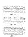
- a conductive barrier layer 3 has both barrier characteristics (to protect the display medium and/or the metal electrode) and the ability to function as an electrode, and is deposited over the substrate to form a composite substrate, as shown in FIG. 19 .
- layer 3 has both low oxygen and moisture permeability, and a low enough resistivity to function as an electrode for the display.
- conductive barrier layer 3 comprises at least one sublayer 3 1 deposited over the substrate, for instance a single ITO layer.
- at least one pair of sublayers (a dyad of a polymer and a TCO, metal, or metal oxide) is deposited over the substrate.
- multiple alternating sublayer pairs comprised of the same materials as the original sublayer pair, are deposited over the substrate or over the previously deposited sublayer.
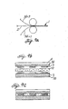
- FIGs. 2-7 illustrate generally only some of the more preferred embodiments of sublayer 3 1 materials for conductive barrier layer 3, while FIGS. 19-33 illustrate particularly the more preferred embodiments for the conductive barrier layer.
- a base coating 20 is deposited over the substrate 38.
- the base coating is a polymer smoothing coating applied by a PML process or an organic hardcoat deposited by a liquid coating process to render a hardcoated PET substrate that is abrasion resistant.
- a TCO 22 (or metal layer 12) is then deposited over the base coat, as shown in FIG. 3 , and more particularly in FIG. 20 .
- multiple alternating layers of a protective polymer layer 24 and an additional TCO 22 (or metal layer 12) are additionally deposited, as represented by sublayer 3 1 in FIG. 3 , and more particularly in FIGs. 21 and 22 .
- the alternating layers are of the same material, e.g. TCO/polymer/TCO, etc.
- FIG. 2 illustrates the embodiment of polymer/TCO/polymer without base coat 20.
- a metal conductor or reflector 12 overlays the top polymer layer 24 as in FIGs. 23-25 , and 30.
- a substrate is coated with a TCO layer, a metal coating, and another TCO layer.
- This three layer configuration is called an "optically enhanced metal," and has characteristics similar to a single TCO layer. With the optically enhanced metal, good conductivity, transmission and barrier properties are achieved.
- Deposited on these three layers is preferably a polymer layer 24, that is alternating with the three layers.
- base coat 20 is deposited over the substrate as shown in FIG. 27 .
- another dyad (a metal and TCO pair) is deposited over the top TCO layer, as shown in FIGs. 28 and 29 . Additionally or alternatively as shown in FIG.
- an additional polymer layer 24 (a polymer overcoat) is deposited over the previously deposited dyad.
- a thick metal layer 12 is deposited over the polymer overcoat layer, as also shown in FIG. 29 .
- a metal nitride layer is substituted for one or more of the metal layers of these embodiments, for example, see FIGs. 31 and 32 .
- a substrate is alternatively coated with an inorganic layer (such as a TCO), and polymer layers to provide both barrier and conductive properties.
- an inorganic layer such as a TCO
- polymer layers to provide both barrier and conductive properties.
- FIG. 33 illustrates a metal layer 12 sandwiched between two metal nitride layers 14.
- additional dyads metal and metal nitride pair
- FIG. 33 illustrates a metal layer 12 sandwiched between two metal nitride layers 14.
- additional dyads metal and metal nitride pair
- FIG. 33 illustrates a metal layer 12 sandwiched between two metal nitride layers 14.
- additional dyads metal and metal nitride pair
- FIG. 33 illustrates a metal layer 12 sandwiched between two metal nitride layers 14.
- additional dyads metal and metal nitride pair
- a dielectric layer replaces one or more TCO layers in the above described embodiments (see generally FIGs. 6 and 7 ).
- multiple alternating layers of dielectric 17 and polymer layers 24 are deposited over the substrate 38.
- the number of multiple alternating layers (or dyads) vary, and is represented here by 3 1 , sublayers of the conductive barrier layer 3.
- a TCO layer 22 is then deposited over the top of multiple alternating layers.
- Each TCO layer 22 of the above embodiments is a single TCO layer.
- the TCO layer represents two TCO layers.
- metal layers that are alternating dyad pairs or in between TCO, metal nitride, or dielectric layers are thin.
- Sublayer 3' materials that provide barrier properties are thin transparent metal oxides 16, and/or thin transparent metallic films 12.
- the polymers 24 enhance barrier properties by reducing the number of holes and defects in the films upon which or under which, they are deposited.
- the metal oxide layers alternatively comprise dielectric layers 17 and/or transparent conductive oxide layers 22.
- the thickness for these barrier layers are in the nanometer and angstrom range.
- the thickness for the PML deposited layers are in the micron range. For example, improved barrier coating occurs when a PML deposited organic polymer layer (a base coat), and/or a metal oxide layer is placed over the plastic substrate. See Tables 2 and 3.
- Sublayer 3 1 materials that provide conductive properties include a thin TCO 22, a thin transparent metallic film 12 (such as aluminum, silver, copper, gold, platinum, palladium, and alloys thereof), and a metal nitride 14 (such as transition metal nitrides, for example, titanium nitride, zirconium nitride, hafnium nitride, and nitrides of Group IVA, VA, and VIA elements of the Periodic Table, as well as nitrides of Group IIIB and IVB elements of the Periodic Table, for example: gallium nitride, silicon nitride, and aluminum nitride).
- the thickness for these conductive layers are in the nanometer and angstrom range.
- the TCO is formed by multiple thin layers deposited with electrical contact to each other, so that a low resistivity is achieved. Consequently, the TCO functions as both the electrode and a barrier.
- the base coat there is a PML processed base coat 20 deposited over the substrate as shown in FIG. 3 .
- the base coat produces substrate smoothing, and more importantly, in combination with other layers, the base coat has surprisingly effective vapor barrier enhancement properties because of the smoothing and protection characteristics.
- the sublayers are deposited in combination with the process illustrated in FIG. 8 .
- Using a smoothing base coat layer over the plastic substrate imparts good optical and barrier quality throughout the substrate layers and provides a pristine surface for nucleation of the deposited TCO electrode layer.
- the pristine surface smooths over any surface roughness of the plastic substrate, thereby adding to the FPD lifetime and optical quality.
- one or more metal oxide layers are replaced with a TCO.
- TCO coatings including ITO ("Tin doped indium oxide"), cadmium oxides (CdSn 2 O 4 , CdGa 2 O 4 , CdIn 2 O 4 , CdSb 2 O 6 , CdGeO 4 ), tin oxides, indium oxides (In 2 O 3 : Ga, GaInO 3 (Sn, Ge), (GaIn) 2 O 3 ), zinc oxides (ZnO(Al), ZnO(Ga), ZnSnO 3 , Zn 2 SnO 4 , Zn 2 In 2 O 3 , Zn 3 In 2 O 6 ), and/or magnesium oxides (MgIn 2 O 4 , MgIn 2 O 4 - Zn 2 In 2 O 5 ) are deposited on a plastic substrate at a low temperature, they have an amorphous micro structure.
- the amorphous structure and oxygen deficiency of the TCO allow the TCO coating to exhibit conductive properties and barrier properties similar to transparent dielectric barrier layers, such as types of silica or alumina. Because of the oxygen deficiency, the barrier layers gather the oxygen and keep the oxygen from passing through. Multiple thin layers of TCO function as a transparent electrode and a transparent barrier layer.
- the benefit of using TCO alternating with metallic film layers, besides the barrier properties, is that all the layers of the structure are conductive, thus improving conductivity.
- a suitable apparatus for coating the substrate with conductive and barrier layers is illustrated schematically in FIG. 8 .
- All of the coating equipment is positioned in a vacuum chamber 36.
- a roll of polypropylene, polyester or other suitable plastic sheet is mounted on a pay-out reel 37.
- Plastic sheet 38 forming the substrate is wrapped around a first rotatable drum 39, and fed to a take-up reel 41.
- a roll 42 is employed, as appropriate, for guiding the sheet material from the payout reel to the drum and/or to the take-up reel.
- a flash evaporator 43 is mounted in proximity to the drum at a first coating station.
- the flash evaporator deposits a layer or film of monomer, typically an acrylate, on the substrate sheet as it travels around the drum.
- the substrate sheet passes an irradiation station where the monomer is irradiated by a source 44 such as an electron gun or source of ultraviolet radiation.
- a source 44 such as an electron gun or source of ultraviolet radiation.
- the radiation or electron bombardment of the film induces polymerization of the monomer.
- the sheet then preferably passes a sputtering station 46 where a coating of TCO is applied by magnetron sputtering.
- the sheet then passes another flash evaporator 47 where another layer of monomer is deposited over the TCO layer.
- a layer of monomer is above or below the TCO layer, either evaporator 43 or 47 is used.
- both evaporators and their respective radiation sources are used.
- the TCO layer is processed by one of thermal evaporation, chemical vapor deposition, plasma enhanced chemical vapor deposition, and electron beam evaporation. Chemical vapor deposition is a high temperature process, and is therefore the least desirable for use with plastic substrates.
- a liquid PML (called Liquid Multilayer, LML) smoothing applicator 52 is mounted in proximity to the drum at a first coating station.
- the liquid smoothing applicator deposits a layer of monomer, e.g. acrylate, over the substrate. This layer of monomer is cured by irradiation from an ultraviolet or electron beam source 48 adjacent the drum.
- the sheet then passes sputtering station 46 where a coating of thin metal film, metal oxide, and/or metal nitride is applied by one of vacuum sputtering, vacuum metallizing, plasma assisted chemical vapor deposition, or electron beam evaporation.
- silicon oxides is deposited by a plasma enhanced chemical vapor deposition process using a metal organic precursor and an oxidizing or inert carrier gas.
- the various layers described are deposited in several processes in addition to vacuum coating techniques.
- the layers are deposited through nonvacuum (atmospheric) roll coating.
- the layers are deposited by an in line coating machine, whereby a conveyor belt runs the substrate to be coated past multiple coating stations.
- the layers are deposited by an intermittent motion machine, that is either in a vacuum processor a nonvacuum process.
- the layers are coated using a multitude of machines. For instance, the plastic substrate is first coated through atmospheric roll coating with a cured polymer and subsequently coated by vacuum deposition, or liquid coated, such as Gravure coating.
- take up reel 41 For multiple layers of organic polymer coatings deposited in the PML process, take up reel 41, with the sheet wound thereon, functions as the pay out reel 37, and the process is repeated as desired by coating in both directions.
- the roll of sheet is removed from the vacuum system for use.
- FIG. 9a illustrates a laminating process for the FPD where the coated plastic substrate and display medium are bonded together with an adhesive, pressure and temperature or through UV radiation.
- FIGs. 9b and 9c are a cross-sectional views of the FPD before and after undergoing the bonding process, respectively.
- the laminating process is one of the alternate methods for bonding the layers to construct the FPD. Because the layers of the present invention are thin; cracking, crazing, and delamination are avoided using processing methods of this type.
- FIGs. 9b and 9c illustrate the flat panel display with a protective overcoat 4 and the display medium 2.
- Transparent dielectric layers with good barrier properties and a high refractive index such as metal oxides like titanium oxide or aluminum oxide, or metal nitrides such as silicon nitride or aluminum nitride, used in combination with thin, transparent metallic film layers provide a transparent conductive barrier coating.
- the metal oxide or metal nitride layers are deposited at specific thicknesses to optimize the optical performance (e.g. transmittance) of a particular display.
- the thin metallic film layer is sandwiched in between layers of metal oxide or metal nitride. Multiple alternating layers of metal oxides or metal nitrides, with their barrier properties, and the highly conductive metallic film layers provide increased barrier performance and conductivity for a particular display medium.
- optical and electrical performance of transparent conductive oxide coatings are also improved by mildly heating during deposition or post-annealing the coated substrate. Even though the substrate was heated to a moderate temperature of only 65 °C, the resistivity of the ITO was still low enough to effectively operate as an electrode, because of the thin layer of ITO. See the Experimental Results below.
- a thin conductive metal nitride layer is substituted for one or more thin metallic film layers.
- Metal oxide orTCO layers are utilized with the metal nitride layer for enhancing both the optical and electrical performance characteristics.
- Metal nitrides have good gas barrier properties. However, to maintain the preferred moisture and oxygen permeability, there is a minimum thickness of the metal nitride layer. Because of the higher optical transparency silicon nitride thin films, for example, are attractive candidates for flexible FPD as barrier layers for atmospheric gases.
- At least one of the metallic film layers is replaced with a polymer layer formed via the PML processes.
- the plastic substrate for a flat panel display has a very low oxygen and water vapor permeability, a surface roughness much less than the barrier film thickness, a high Tg (the glass transition temperature) to allow a higher temperature and/or higher energy ITO deposition process, and a high transparency with low ND (index of refraction) birefringence.
- Defects in the coated layers limit the barrier properties. For instance, rough substrates, particulates, and roller contact damage the coated layers. Rough substrates with thin film barriers are smoothed and prevented from damage by roller contact with an organic basecoat and polymer top coat multilayers, respectively.
- TCO's deposited on the substrate achieve lower surface resistivity than a single thick layer of TCO. Further, the multiple TCO layers act as electrodes connected in parallel.
- non-stoichiometric dielectric of a group including silicon oxides, aluminum oxides, and silicon nitrides allow for the fabrication all efficient thin film barriers for flexible plastic films.
- the optical, electrical and barrier properties were measured for ITO sputter-deposited directly onto a PET substrate, and also measured with a PML acrylic base coat over the substrate before deposition of the ITO, in a roll-to-roll (web) coating process. See FIGS. 10-13 , and descriptions of the Figures below.
- the typical performance of a single ITO layer deposited on a base coated PET substrate is ⁇ 85%T (Transmittance) and ⁇ 80 ohms/square.
- the ITO layer has a physical thickness of about 140 nm, for a one-half wave optical thickness, while the PET substrate has a thickness of about 0.007".
- oxygen permeability ranged from 0.005 to 0.05 oxygen cc/m 2 /day, while the water permeability ranged from 0.005 to 0.05 g/m 2 /day.
- FIG. 10 discloses a chart showing water permeability of ITO film, as well as ITO sandwiching a silver layer, each deposited on a PET substrate versus ITO film resistance. No smoothing base coat was applied to the substrate in either case.
- the ITO layer was DC sputter deposited onto a PET substrate.
- the deposited ITO film is sputtered from a metal target in a web coater.
- the vertical lines shown connect the midpoints of the range of permeability results at each measured resistance for the ITO film sheet.
- the chart shows that the permeability dips to a minimal value of approximately 0.006 g/m 2 day at a resistance of about 60 ohms/square.
- the permeability reaches a maximum of approximately 0.21 g/m 2 day at a resistance of about 350 ohms/square.
- the approximate permeability range was 0.04 to 0.075 g/m 2 day for the sheet resistance at about 12 ohms/square.
- FIG. 11 discloses a chart showing water permeability of ITO film, as well as ITO sandwiching a silver layer, each deposited on a PET substrate versus ITO film sheet thickness.
- the ITO layer alone is analyzed in the same manner as above.
- the chart shows that the permeability dips to a minimal value of approximately 0.006 g/m 2 day at a thickness of about 120 nm.
- the permeability reaches a maximum of approximately 0.21 g/m 2 day at a thickness of about 40 nm.
- the approximate permeability range was 0.04 to 0.075 g/m 2 day for a sheet thickness of approximately 120 nm.
- FIGs. 12 and 13 disclose charts showing oxygen permeability of ITO film deposited on a PET substrate versus ITO film sheet thickness and sheet resistivity, respectively.
- FIG. 12 shows that the permeability dips to a minimal value of approximately 0.017 g/m 2 day at a thickness of about 220 nm. The permeability reaches a maximum of approximately 0.9 cc/m 2 day at a thickness of about 40 nm.
- alternating barrier layers of PML deposited organic polymers and dielectrics have permeation rates below the limits of the instruments, which is 0.005 g/m 2 *day for Permatran-W 3/31, an instrument for measuring water vapor transmission rates and 0.005 cc/m 2 *day for Ox-Tran 2/20, an instrument for measuring oxygen transmission rates.
- a transparent dielectric barrier layer or a "single layer" of TCO deposited on the substrate has suitable barrier properties for the plastic FPD.
- the preferable barrier properties vary by the type of display technology: liquid crystal display (LCD) and organic light emitting display (OLED).
- the acceptable value of vapor permeation with plastic substrates for FPD depends on the sensitivity of the specific display technology utilized. For example, the LCD is much less sensitive to vapor permeation than the OLED.
- oxygen permeability is preferably in the range of about 0.01 to 0.1 cc/m 2 *day, while water vapor permeability is preferably in the range of about 0.01 to 0.1 glm 2 *day.
- permeabilities of ⁇ 0.001 cc/m 2 *day for oxygen, and ⁇ 0.001 g/m 2 *day for moisture (water vapor) are preferred.
- a polymer OLED and a small molecule OLED describes the two basic technologies for the layer that emits light in the OLED.
- the light emitting material is deposited by flow coating, spin coating, gravure coating, meniscus coating, curtain coating or any common liquid coating or printing techniques.
- the small molecule OLED is normally thermally evaporated in'a vacuum, but is also processed with nonvacuum coating methods. If the ITO layer is deposited by nonvacuum processes such as by screen printing, the process of the present invention is entirely nonvacuum.
- the process of the present invention takes place by both vacuum and nonvacuum methods. Preferably, the process takes place in a vacuum both to avoid contamination by particulates, and to avoid moisture and oxygen. Superior barrier films and other films are provided by the cleaner vacuum process.
- the preferred water permeability for the LCD is met.
- the preferred oxygen permeability for the LCD is met as long as the ITO film thickness is above about 85 nm and as long as the sheet resistance is below about 150 ohm/square.
- the barrier capability is enhanced by multilayer dielectric or TCO barriers in combination with PML processed polymer coatings (i.e. composite barrier layers of PML deposited organic polymer layers, dielectric layers and/or TCO layers).
- Two charts of a test illustrate water vapor and oxygen permeability versus ITO thickness.
- the measured results for semi-reactively and reactively sputtered ITO, as well as the differences between a single ITO layer and two ITO layers (with a polymer layer in between the two layers) made with a semi-reactive process, are as follows; 'Semi-reactively' sputtered refers to DC magnetron sputtered from a ceramic target.
- the differences between the two processes are due to the specific process parameters, and not inherent to the process type.
- the two ITO layers have higher conductivity and lower permeability as compared to the single ITO layer. Further, the two ITO layers have higher electrical performance, because the single ITO layer cracks and/or crazes.
- the preferred thickness for the deposited layers is different for conductivity and barrier properties.
- the deposited film is thick in order to have conductive properties. Also, if a film layer is too thin it will not have adequate barrier properties.
- the critical thickness for these layers varies with the material and, to a lesser extent, how the layer is deposited.
- the critical minimal thickness is about 20 nanometers (or 200 angstroms).
- the lower limits for some of the metal oxides are about 10 to 30 nanometer range in packaging. Generally, 5-10 nanometers is the minimum thickness for adequate barrier properties.
- enhanced conductive properties result film thickness in the range of about 20 nanometers to 300 nanometers. If the film is thicker than that range, then the film starts cracking, and hence, loses conductivity and barrier properties. For maximizing optical transmission, it is well known that optical thicknesses of thin films are selected.
- the typical physical thickness is 20-300 nanometers for ITO on a flexible substrate.
- the percentage of spectral transmittance and reflectance remains relatively constant.
- the transmittance percentage is about 80% for resistance ranging from 29 ohms/square to 347 ohms/square.
- DC sputter deposited ITO on a hardcoated PET substrate exhibited a resistivity of 46.9 Ohms/square, which is approximately 5X10 -4 ohm-cm, and a visible transmittance of 84.7%.
- the transmittance increases (and the reflectance decreases) as the plasma wavelength increases. There is always a compromise between high optical transmittance and high conductivity.
- FIG. 14 (a more preferred embodiment of the present invention) at the higher wavelengths, the transmittance decreases (and the reflectance increases).
- Another test illustrates the Transmittance and Reflectance of semi-reactively sputtered ITO on a PET substrate for various thicknesses versus wavelength.
- the transmittance and reflectance of a substrate coated with a polymer layer and an ITO layer, a substrate with an ITO layer, and a substrate with two ITO layers (with a polymer layer in between the two ITO layers) are illustrated.
- transmittance and conductivity are inversely related.
- Improved optical performance is achieved by controlling the thickness and index of the polymer layers.
- a transparent electrode conductivity varies with display technology and addressing method,
- the surface resistivity for LCD's is about 50-300 Ohm/square, and for OLED's is about 10-100 Ohm/square.
- the corresponding visible transmittance for LCD's is about 90%, and for OLED's is about 80-85%.
- the thickness of the conductor layer is compatible with the vacuum web coating processing for the flexible plastic substrate.
- Table 1 shows the test results for oxygen and water vapor transmission rates of various samples of a substrate coated with a single ITO layer with different ohm/square coatings and a substrate coated with an ITO layer, a metal layer, and another ITO layer.
- the test conditions were as follows: the temperature was at 23°C/73.4°F.
- the relative humidity was 0%.
- the relative humidity was 100%, but the other side of the barrier had a relative humidity of 0%.
- the first eight samples are a single layer ITO with different resistances coated onto a plastic substrate.
- the '25-1' is the first sample of the resistance of 25 ohm/square; whereas '25-2' is the second sample from the same lot.
- the last two samples are of a substrate coated with an ITO layer, a metal coating, and another ITO layer, with a resistance of 10 ohm/square.
- This 3 layer configuration is called "optically enhanced metal,” or "induced transmission filter,” and has similar characteristics as a single TCO layer. With the optically enhanced metal good conductivity, transmission and barrier properties are achieved.
- the ITO layers, which antireflect the metal each have a thickness of about 30-60 nanometers. In several instances, the samples were tested two times.
- the second column for the 25 and 60 ohm/square reflects the results of the second test.
- Table 1 Sample Water Vapor Transmission Rate (g/m 2 *day) Oxygen Transmission Rate (cc/m 2 *day) 25-1 0.026 ⁇ 0.005 1 0.017 0.087 25-2 0.097 ⁇ 0.005 1 0.584 0.257 60-1 0.042 0.059 0.071 60-2 0.050 0.204 0.090 60-3 0.007 ⁇ 0.005 2 60-4 ⁇ 0.005 1 0.014 300-1 0.243 0.861 300-2 0.232 0.864 M-10-1 0.076 0.035 M-10-2 0.041 0.024 1
- the actual water vapor transmission rate was at least as low as the lower limit of the instrument.
- the actual oxygen transmission rate was at least as low as the lower limit of the instrument.
- Table 2 compares permeation rates for different coatings, including multiple dyad (an acrylate/oxide pair) layers, on polyethylene terephthalate (PET) and oriented polypropylene (OPP) substrates. As shown, a single dyad on a substrate has high permeation resistance for oxygen and moisture. In some instances, two oxygen transmission rate tests were conducted, and the results were shown in a second column. Footnote 1 denotes the typical permeation rate for the PET substrate.
- Samples A through D are layers of polymer (PML)/oxide/polymer (PML) on 2 mil PET.
- Samples E through H are 2 mil PET only.
Claims (32)
- Substrat composite pour une utilisation dans les affichages à écran plat (1), l'emballage ou les lampes à électroluminescence comprenant :un substrat en plastique (38) ; etune première couche de matériau de barrière conducteur (3) déposée sur le substrat en plastique (38), la couche de matériau de barrière conducteur (3) incluant un matériau parmi un oxyde conducteur transparent mince (22) et un nitrure de métal (14) caractérisé en ce que le substrat composite comprend en outre plusieurs paires de sous-couches alternées d'un monomère organique réticulé déposé en phase vapeur et d'un oxyde conducteur transparent (22).
- Substrat composite selon la revendication 1, comprenant en outre un premier polymère organique déposé au-dessus du substrat en plastique (38).
- Substrat composite selon la revendication 1, comprenant en outre un premier polymère organique déposé au-dessus de la couche de barrière conductrice (3).
- Substrat composite selon la revendication 2, comprenant en outre un deuxième polymère organique déposé au-dessus de la couche de barrière conductrice (3).
- Substrat composite selon la revendication 1, comprenant en outre une ou plusieurs couches supplémentaires de matériau de barrière conducteur déposé au-dessus du substrat en plastique (38), les couches supplémentaires de matériau de barrière conducteur possédant le même matériau que le premier matériau de barrière conducteur (3).
- Substrat composite selon la revendication 5, comprenant en outre une ou plusieurs couches supplémentaires déposées au-dessus de la couche de matériau de barrière conducteur précédemment déposée, respectivement, chaque couche supplémentaire incluant un matériau parmi un polymère organique, un diélectrique transparent mince, un film métallique transparent mince (12) et un oxyde conducteur transparent mince (22).
- Substrat composite selon la revendication 6, dans lequel le film métallique transparent mince (12) est de l'aluminium.
- Substrat composite selon la revendication 6, dans lequel le film métallique transparent mince (12) est de l'argent.
- Substrat composite selon la revendication 1, dans lequel le substrat en plastique (38) est un matériau parmi un polyester et une polyoléfine.
- Substrat composite selon la revendication 1, dans lequel l'oxyde conducteur transparent (22) est de l'oxyde d'indium dopé à l'étain.
- Substrat composite selon la revendication 6, dans lequel la barrière diélectrique transparente est un matériau parmi l'oxyde de silicium et l'oxyde d'aluminium.
- Procédé de fabrication d'un substrat composite pour une utilisation dans un affichage à écran plat (1) ou un emballage, comprenant :la fourniture d'un substrat en plastique (38) ; etle dépôt d'une première couche de matériau de barrière conducteur (3) sur le substrat en plastique (38), la couche de matériau de barrière conducteur (3) incluant un matériau parmi un oxyde conducteur transparent mince (22) et un nitrure de métal (14), caractérisé en ce que le procédé comprend en outre le dépôt de plusieurs paires de sous-couches alternées d'un monomère organique réticulé déposé en phase vapeur et d'un oxyde conducteur transparent (22).
- Procédé selon la revendication 12, comprenant en outre le dépôt d'un premier polymère organique au-dessus du substrat en plastique (38).
- Procédé selon la revendication 12, comprenant en outre le dépôt d'un premier polymère organique au-dessus de la couche de barrière conductrice (3).
- Procédé selon la revendication 13, comprenant en outre le dépôt d'un deuxième polymère organique au-dessus de la couche de barrière conductrice (3).
- Procédé selon la revendication 12, comprenant en outre le dépôt d'une ou plusieurs couches supplémentaires de matériau de barrière conducteur au-dessus du substrat en plastique (38), les couches supplémentaires de matériau de barrière conducteur possédant le même matériau que le premier matériau de barrière conducteur (3).
- Procédé selon la revendication 16, comprenant en outre le dépôt d'une ou plusieurs couches supplémentaires au-dessus de la couche de matériau de barrière conducteur précédemment déposée, respectivement, chaque couche supplémentaire incluant un matériau parmi un polymère organique, un diélectrique transparent mince, un film métallique transparent mince (12) et un oxyde conducteur transparent mince (22).
- Procédé selon la revendication 13, comprenant en outre le dépôt en phase vapeur et la réticulation d'un monomère organique pour former la couche polymère.
- Procédé selon la revendication 13, comprenant en outre le lissage par liquide d'un polymère organique de façon à former la couche polymère.
- Procédé selon la revendication 13, comprenant en outre le dépôt de la couche polymère au-dessus de la couche précédemment déposée avant que la couche précédemment déposée ne vienne en contact avec une surface.
- Procédé selon la revendication 17, dans lequel le film métallique transparent mince (12) est de l'aluminium.
- Procédé selon la revendication 17, dans lequel le film métallique transparent mince (12) est de l'argent.
- Procédé selon la revendication 12, dans lequel le substrat en plastique (38) est un matériau parmi un polyester et une polyoléfine.
- Procédé selon la revendication 12, dans lequel le revêtement d'oxyde conducteur transparent (22) est de l'oxyde d'indium dopé à l'étain.
- Procédé selon la revendication 17, dans lequel la barrière diélectrique transparente est un matériau parmi l'oxyde de silicium et l'oxyde d'aluminium.
- Procédé selon la revendication 25, comprenant en outre le dépôt de l'oxyde d'aluminium par un procédé d'évaporation de l'aluminium qui est ensuite converti en un oxyde dans un plasma d'oxygène et une évaporation par faisceau d'électrons.
- Procédé selon la revendication 17, comprenant en outre le dépôt de la couche diélectrique par un procédé de dépôt chimique en phase vapeur assisté par plasma en utilisant un matériau parmi un gaz vecteur oxydant et un gaz vecteur inerte.
- Procédé selon la revendication 21, comprenant en outre le dépôt de la couche d'aluminium par un procédé parmi la métallisation sous vide et la pulvérisation.
- Procédé selon la revendication 12, dans lequel l'oxyde conducteur transparent (22) est déposé par pulvérisation.
- Procédé selon la revendication 29, comprenant en outre la fourniture d'hydrogène dans un plasma d'une chambre à vide utilisée dans le procédé de pulvérisation de l'oxyde conducteur transparent (22).
- Procédé selon la revendication 12, comprenant en outre un recuit modéré du substrat (38) avant dépôt des couches sur celui-ci.
- Procédé selon la revendication 31, dans lequel le substrat (38) est recuit à approximativement 65 °C.
Applications Claiming Priority (5)
| Application Number | Priority Date | Filing Date | Title |
|---|---|---|---|
| US419870 | 1995-04-11 | ||
| US10687198P | 1998-11-02 | 1998-11-02 | |
| US106871P | 1998-11-02 | ||
| US41987099A | 1999-10-18 | 1999-10-18 | |
| PCT/US1999/025843 WO2000026973A1 (fr) | 1998-11-02 | 1999-11-02 | Oxydes conducteurs transparents pour ecran plat en plastique |
Publications (2)
| Publication Number | Publication Date |
|---|---|
| EP1127381A1 EP1127381A1 (fr) | 2001-08-29 |
| EP1127381B1 true EP1127381B1 (fr) | 2015-09-23 |
Family
ID=26804119
Family Applications (1)
| Application Number | Title | Priority Date | Filing Date |
|---|---|---|---|
| EP99956881.9A Expired - Lifetime EP1127381B1 (fr) | 1998-11-02 | 1999-11-02 | Oxydes conducteurs transparents pour ecran plat en plastique |
Country Status (5)
| Country | Link |
|---|---|
| US (5) | US7186465B2 (fr) |
| EP (1) | EP1127381B1 (fr) |
| AU (1) | AU1339700A (fr) |
| CA (1) | CA2353506A1 (fr) |
| WO (1) | WO2000026973A1 (fr) |
Cited By (2)
| Publication number | Priority date | Publication date | Assignee | Title |
|---|---|---|---|---|
| US9184410B2 (en) | 2008-12-22 | 2015-11-10 | Samsung Display Co., Ltd. | Encapsulated white OLEDs having enhanced optical output |
| US9337446B2 (en) | 2008-12-22 | 2016-05-10 | Samsung Display Co., Ltd. | Encapsulated RGB OLEDs having enhanced optical output |
Families Citing this family (216)
| Publication number | Priority date | Publication date | Assignee | Title |
|---|---|---|---|---|
| US20040241454A1 (en) * | 1993-10-04 | 2004-12-02 | Shaw David G. | Barrier sheet and method of making same |
| CA2353506A1 (fr) * | 1998-11-02 | 2000-05-11 | 3M Innovative Properties Company | Oxydes conducteurs transparents pour ecran plat en plastique |
| TW439308B (en) * | 1998-12-16 | 2001-06-07 | Battelle Memorial Institute | Environmental barrier material for organic light emitting device and method of making |
| US6413645B1 (en) * | 2000-04-20 | 2002-07-02 | Battelle Memorial Institute | Ultrabarrier substrates |
| US7198832B2 (en) * | 1999-10-25 | 2007-04-03 | Vitex Systems, Inc. | Method for edge sealing barrier films |
| US6548912B1 (en) * | 1999-10-25 | 2003-04-15 | Battelle Memorial Institute | Semicoductor passivation using barrier coatings |
| US6866901B2 (en) * | 1999-10-25 | 2005-03-15 | Vitex Systems, Inc. | Method for edge sealing barrier films |
| US20100330748A1 (en) * | 1999-10-25 | 2010-12-30 | Xi Chu | Method of encapsulating an environmentally sensitive device |
| US20070196682A1 (en) * | 1999-10-25 | 2007-08-23 | Visser Robert J | Three dimensional multilayer barrier and method of making |
| US20090191342A1 (en) * | 1999-10-25 | 2009-07-30 | Vitex Systems, Inc. | Method for edge sealing barrier films |
| US6867539B1 (en) | 2000-07-12 | 2005-03-15 | 3M Innovative Properties Company | Encapsulated organic electronic devices and method for making same |
| JP2002187231A (ja) * | 2000-10-13 | 2002-07-02 | Dainippon Printing Co Ltd | バリア性フィルムおよびその製造法 |
| US6537688B2 (en) | 2000-12-01 | 2003-03-25 | Universal Display Corporation | Adhesive sealed organic optoelectronic structures |
| US6614057B2 (en) | 2001-02-07 | 2003-09-02 | Universal Display Corporation | Sealed organic optoelectronic structures |
| US6576351B2 (en) | 2001-02-16 | 2003-06-10 | Universal Display Corporation | Barrier region for optoelectronic devices |
| US6624568B2 (en) | 2001-03-28 | 2003-09-23 | Universal Display Corporation | Multilayer barrier region containing moisture- and oxygen-absorbing material for optoelectronic devices |
| US6664137B2 (en) | 2001-03-29 | 2003-12-16 | Universal Display Corporation | Methods and structures for reducing lateral diffusion through cooperative barrier layers |
| CA2352567A1 (fr) | 2001-07-06 | 2003-01-06 | Mohamed Latreche | Matiere translucide possedant de tres bonnes proprietes barrieres contre la diffusion de gaz et de vapeurs et methode de production de ladite matiere |
| US6844203B2 (en) * | 2001-08-30 | 2005-01-18 | Micron Technology, Inc. | Gate oxides, and methods of forming |
| US8026161B2 (en) | 2001-08-30 | 2011-09-27 | Micron Technology, Inc. | Highly reliable amorphous high-K gate oxide ZrO2 |
| US20090208754A1 (en) * | 2001-09-28 | 2009-08-20 | Vitex Systems, Inc. | Method for edge sealing barrier films |
| CN100378551C (zh) * | 2001-10-22 | 2008-04-02 | 三星电子株式会社 | 液晶显示器及其制造方法 |
| US6888305B2 (en) | 2001-11-06 | 2005-05-03 | Universal Display Corporation | Encapsulation structure that acts as a multilayer mirror |
| US20030089252A1 (en) * | 2001-11-09 | 2003-05-15 | Sarnecki Greg J. | Production of Electroluminescent Devices |
| US6597111B2 (en) | 2001-11-27 | 2003-07-22 | Universal Display Corporation | Protected organic optoelectronic devices |
| US6753096B2 (en) | 2001-11-27 | 2004-06-22 | General Electric Company | Environmentally-stable organic electroluminescent fibers |
| US7053547B2 (en) | 2001-11-29 | 2006-05-30 | Universal Display Corporation | Increased emission efficiency in organic light-emitting devices on high-index substrates |
| CN100381898C (zh) * | 2001-11-29 | 2008-04-16 | 大宇电子Service株式会社 | 制造塑料基板的方法 |
| US6953730B2 (en) * | 2001-12-20 | 2005-10-11 | Micron Technology, Inc. | Low-temperature grown high quality ultra-thin CoTiO3 gate dielectrics |
| US6765351B2 (en) * | 2001-12-20 | 2004-07-20 | The Trustees Of Princeton University | Organic optoelectronic device structures |
| TW520616B (en) * | 2001-12-31 | 2003-02-11 | Ritdisplay Corp | Manufacturing method of organic surface light emitting device |
| WO2003057472A1 (fr) * | 2002-01-07 | 2003-07-17 | Hanita Coatings | Film de protection statique, transparent, presentant des proprietes barrieres |
| US7012363B2 (en) | 2002-01-10 | 2006-03-14 | Universal Display Corporation | OLEDs having increased external electroluminescence quantum efficiencies |
| US6767795B2 (en) * | 2002-01-17 | 2004-07-27 | Micron Technology, Inc. | Highly reliable amorphous high-k gate dielectric ZrOXNY |
| JP3627707B2 (ja) | 2002-01-23 | 2005-03-09 | 富士電機ホールディングス株式会社 | 色変換フィルタ基板、それを用いた有機多色elディスプレイパネルおよびそれらの製造方法 |
| US6812100B2 (en) * | 2002-03-13 | 2004-11-02 | Micron Technology, Inc. | Evaporation of Y-Si-O films for medium-k dielectrics |
| EP2249413A3 (fr) | 2002-04-01 | 2011-02-02 | Konica Corporation | Support et élément électroluminescent organique comprenant ce support |
| US6897474B2 (en) | 2002-04-12 | 2005-05-24 | Universal Display Corporation | Protected organic electronic devices and methods for making the same |
| US6835950B2 (en) | 2002-04-12 | 2004-12-28 | Universal Display Corporation | Organic electronic devices with pressure sensitive adhesive layer |
| US8900366B2 (en) | 2002-04-15 | 2014-12-02 | Samsung Display Co., Ltd. | Apparatus for depositing a multilayer coating on discrete sheets |
| US8808457B2 (en) | 2002-04-15 | 2014-08-19 | Samsung Display Co., Ltd. | Apparatus for depositing a multilayer coating on discrete sheets |
| US20030203210A1 (en) * | 2002-04-30 | 2003-10-30 | Vitex Systems, Inc. | Barrier coatings and methods of making same |
| US7589029B2 (en) * | 2002-05-02 | 2009-09-15 | Micron Technology, Inc. | Atomic layer deposition and conversion |
| US7160577B2 (en) * | 2002-05-02 | 2007-01-09 | Micron Technology, Inc. | Methods for atomic-layer deposition of aluminum oxides in integrated circuits |
| JP4052021B2 (ja) * | 2002-06-04 | 2008-02-27 | 帝人デュポンフィルム株式会社 | 配向ポリエステルフィルムおよびそれを用いた積層フィルム |
| US7135421B2 (en) * | 2002-06-05 | 2006-11-14 | Micron Technology, Inc. | Atomic layer-deposited hafnium aluminum oxide |
| US7217344B2 (en) * | 2002-06-14 | 2007-05-15 | Streaming Sales Llc | Transparent conductive film for flat panel displays |
| US6811815B2 (en) | 2002-06-14 | 2004-11-02 | Avery Dennison Corporation | Method for roll-to-roll deposition of optically transparent and high conductivity metallic thin films |
| US7221586B2 (en) * | 2002-07-08 | 2007-05-22 | Micron Technology, Inc. | Memory utilizing oxide nanolaminates |
| US7399500B2 (en) * | 2002-08-07 | 2008-07-15 | Schott Ag | Rapid process for the production of multilayer barrier layers |
| US6929864B2 (en) | 2002-08-17 | 2005-08-16 | 3M Innovative Properties Company | Extensible, visible light-transmissive and infrared-reflective film and methods of making and using the film |
| US6818291B2 (en) | 2002-08-17 | 2004-11-16 | 3M Innovative Properties Company | Durable transparent EMI shielding film |
| US6933051B2 (en) * | 2002-08-17 | 2005-08-23 | 3M Innovative Properties Company | Flexible electrically conductive film |
| US7215473B2 (en) | 2002-08-17 | 2007-05-08 | 3M Innovative Properties Company | Enhanced heat mirror films |
| US7015640B2 (en) | 2002-09-11 | 2006-03-21 | General Electric Company | Diffusion barrier coatings having graded compositions and devices incorporating the same |
| US6958302B2 (en) * | 2002-12-04 | 2005-10-25 | Micron Technology, Inc. | Atomic layer deposited Zr-Sn-Ti-O films using TiI4 |
| US6975067B2 (en) | 2002-12-19 | 2005-12-13 | 3M Innovative Properties Company | Organic electroluminescent device and encapsulation method |
| US20040121146A1 (en) * | 2002-12-20 | 2004-06-24 | Xiao-Ming He | Composite barrier films and method |
| SG112874A1 (en) * | 2003-02-20 | 2005-07-28 | Sony Corp | Reducing water permeation into electronic devices |
| US7018713B2 (en) | 2003-04-02 | 2006-03-28 | 3M Innovative Properties Company | Flexible high-temperature ultrabarrier |
| US6888172B2 (en) * | 2003-04-11 | 2005-05-03 | Eastman Kodak Company | Apparatus and method for encapsulating an OLED formed on a flexible substrate |
| US7510913B2 (en) * | 2003-04-11 | 2009-03-31 | Vitex Systems, Inc. | Method of making an encapsulated plasma sensitive device |
| US7648925B2 (en) | 2003-04-11 | 2010-01-19 | Vitex Systems, Inc. | Multilayer barrier stacks and methods of making multilayer barrier stacks |
| US7051282B2 (en) * | 2003-06-13 | 2006-05-23 | Microsoft Corporation | Multi-layer graphical user interface |
| GB2403594B (en) * | 2003-07-03 | 2006-04-26 | Fuji Electric Co Ltd | Color-converting filter substrate,multi-color organic el display panel using the color-converting filter substrate,and manufacturing methods thereof |
| US7052772B2 (en) | 2003-08-14 | 2006-05-30 | 3M Innovative Properties Company | Material for packaging electronic components |
| US6998648B2 (en) | 2003-08-25 | 2006-02-14 | Universal Display Corporation | Protected organic electronic device structures incorporating pressure sensitive adhesive and desiccant |
| US20050051763A1 (en) * | 2003-09-05 | 2005-03-10 | Helicon Research, L.L.C. | Nanophase multilayer barrier and process |
| JP4703108B2 (ja) * | 2003-09-10 | 2011-06-15 | 三星モバイルディスプレイ株式會社 | 発光素子基板およびそれを用いた発光素子 |
| JP2005108644A (ja) * | 2003-09-30 | 2005-04-21 | Sanyo Electric Co Ltd | 有機el素子 |
| EP1697813A1 (fr) * | 2003-12-19 | 2006-09-06 | Koninklijke Philips Electronics N.V. | Afficheur securise |
| EP1712109A4 (fr) * | 2003-12-30 | 2008-03-19 | Agency Science Tech & Res | Dispositifs electroluminescents souples |
| US20050214556A1 (en) * | 2004-02-20 | 2005-09-29 | Fuji Photo Film Co., Ltd | Organic-inorganic composite composition, plastic substrate, gas barrier laminate film, and image display device |
| US7135352B2 (en) * | 2004-02-26 | 2006-11-14 | Eastman Kodak Company | Method of fabricating a cover plate bonded over an encapsulated OLEDs |
| US20050228465A1 (en) * | 2004-04-09 | 2005-10-13 | Christa Harris | Thermal device for activatable thermochemical compositions |
| DE102004025578B4 (de) * | 2004-05-25 | 2009-04-23 | Applied Materials Gmbh & Co. Kg | Verfahren zum Herstellen von organischen, Licht emittierenden Flächenelementen und Verwendung dieses Verfahrens |
| US7169232B2 (en) * | 2004-06-01 | 2007-01-30 | Eastman Kodak Company | Producing repetitive coatings on a flexible substrate |
| US7378157B2 (en) * | 2004-06-28 | 2008-05-27 | Dai Nippon Printing Co., Ltd. | Gas barrier film, and display substrate and display using the same |
| US20070160786A1 (en) * | 2004-07-04 | 2007-07-12 | Gila Levin | Semi-transparent shielding bag formed by translucent barrier statis shielding film |
| DE102004036170B4 (de) * | 2004-07-26 | 2007-10-11 | Schott Ag | Vakuumbeschichtungsanlage und Verfahren zur Vakuumbeschichtung und deren Verwendung |
| KR100601324B1 (ko) * | 2004-07-27 | 2006-07-14 | 엘지전자 주식회사 | 유기 전계 발광 소자 |
| US8748003B2 (en) | 2004-09-01 | 2014-06-10 | Konica Minolta Holdings, Inc. | Gas barrier laminate and production method of the same |
| EP1819508A1 (fr) * | 2004-11-19 | 2007-08-22 | Akzo Nobel N.V. | Procédé de fabrication de matériau souple en couches, transparent compensé mécaniquement |
| US7695805B2 (en) * | 2004-11-30 | 2010-04-13 | Tdk Corporation | Transparent conductor |
| DE102004059876B4 (de) * | 2004-12-10 | 2010-01-28 | W.C. Heraeus Gmbh | Verwendung eines Sputtertargets aus einer Silberlegierung sowie Glassubstrat mit Wärmedämmschicht |
| JP4837295B2 (ja) * | 2005-03-02 | 2011-12-14 | 株式会社沖データ | 半導体装置、led装置、ledヘッド、及び画像形成装置 |
| JP4425167B2 (ja) * | 2005-03-22 | 2010-03-03 | 富士フイルム株式会社 | ガスバリア性フィルム、基材フィルムおよび有機エレクトロルミネッセンス素子 |
| US7531239B2 (en) * | 2005-04-06 | 2009-05-12 | Eclipse Energy Systems Inc | Transparent electrode |
| JP4663381B2 (ja) * | 2005-04-12 | 2011-04-06 | 富士フイルム株式会社 | ガスバリア性フィルム、基材フィルムおよび有機エレクトロルミネッセンス素子 |
| US20080280073A1 (en) * | 2005-04-18 | 2008-11-13 | Sumitomo Chemical Company, Limited | Substrate and Display Device |
| JP4698310B2 (ja) * | 2005-07-11 | 2011-06-08 | 富士フイルム株式会社 | ガスバリア性フィルム、基材フィルムおよび有機エレクトロルミネッセンス素子 |
| US20070020451A1 (en) * | 2005-07-20 | 2007-01-25 | 3M Innovative Properties Company | Moisture barrier coatings |
| US7927948B2 (en) | 2005-07-20 | 2011-04-19 | Micron Technology, Inc. | Devices with nanocrystals and methods of formation |
| US20070030568A1 (en) * | 2005-07-26 | 2007-02-08 | Tohoku University Future Vision Inc. | High-reflectance visible-light reflector member, liquid-crystal display backlight unit employing the same, and manufacture of the high-reflectance visible-light reflector member |
| US7744955B2 (en) * | 2005-08-02 | 2010-06-29 | Guardian Industries Corp. | Method of thermally tempering coated article with transparent conductive oxide (TCO) coating using flame(s) in tempering furnace adjacent TCO to burn off oxygen and product made using same |
| JP4356113B2 (ja) * | 2005-08-08 | 2009-11-04 | セイコーエプソン株式会社 | 製膜方法、パターニング方法、光学装置の製造方法、および電子装置の製造方法 |
| US7767498B2 (en) | 2005-08-25 | 2010-08-03 | Vitex Systems, Inc. | Encapsulated devices and method of making |
| KR101168731B1 (ko) * | 2005-09-06 | 2012-07-26 | 삼성전자주식회사 | 액정표시장치용 기판 |
| WO2007030458A2 (fr) * | 2005-09-06 | 2007-03-15 | Trustees Of Boston University | Plasmons a surface accordable pouvant ameliorer le rendement d'emission de lumiere |
| TWI326379B (en) * | 2005-09-20 | 2010-06-21 | Au Optronics Corp | A double-sided liquid crystal display |
| US20070096646A1 (en) * | 2005-10-28 | 2007-05-03 | Van Nice Harold L | Electroluminescent displays |
| CN101351868B (zh) * | 2005-12-29 | 2013-03-13 | 3M创新有限公司 | 使用涂覆工艺雾化材料的方法 |
| JP4717674B2 (ja) * | 2006-03-27 | 2011-07-06 | 富士フイルム株式会社 | ガスバリア性フィルム、基材フィルムおよび有機エレクトロルミネッセンス素子 |
| US20080006819A1 (en) * | 2006-06-19 | 2008-01-10 | 3M Innovative Properties Company | Moisture barrier coatings for organic light emitting diode devices |
| WO2008007770A1 (fr) * | 2006-07-14 | 2008-01-17 | Dai Nippon Printing Co., Ltd. | Film revêtu d'une couche conductrice transparente et son utilisation |
| EP2070104A2 (fr) * | 2006-07-25 | 2009-06-17 | David W. Cunningham | Lampe a incandescence integrant un systeme de revetement reflechissant l'infrarouge et appareil d'eclairage comportant une telle lampe |
| WO2008023802A1 (fr) * | 2006-08-25 | 2008-02-28 | Nalux Co., Ltd. | Dispositif optique à film multicouche et procédé pour produire celui-ci |
| US8088502B2 (en) | 2006-09-20 | 2012-01-03 | Battelle Memorial Institute | Nanostructured thin film optical coatings |
| KR100824880B1 (ko) * | 2006-11-10 | 2008-04-23 | 삼성에스디아이 주식회사 | 유기 전계 발광 표시 장치 및 그 제조 방법 |
| KR100824881B1 (ko) * | 2006-11-10 | 2008-04-23 | 삼성에스디아이 주식회사 | 유기 전계 발광 표시 장치 및 그 제조 방법 |
| KR100833738B1 (ko) * | 2006-11-30 | 2008-05-29 | 삼성에스디아이 주식회사 | 유기 전계 발광 표시 장치 및 그 제조 방법 |
| KR100824902B1 (ko) * | 2006-12-13 | 2008-04-23 | 삼성에스디아이 주식회사 | 유기 전계 발광 표시 장치 및 그 제조 방법 |
| EP2125361B1 (fr) | 2006-12-28 | 2019-01-23 | 3M Innovative Properties Company | Couche de nucléation pour la formation d'une couche métallique à film mince |
| BRPI0721301A2 (pt) | 2006-12-29 | 2014-03-25 | 3M Innovative Properties Co | Método para cura de filmes contendo alcóxido metálico |
| BRPI0720867A2 (pt) * | 2006-12-29 | 2014-03-04 | 3M Innovative Properties Company. | Método para fabricação de filmes inorgânicos ou híbridos inorgânicos/orgânicos |
| US8747630B2 (en) | 2007-01-16 | 2014-06-10 | Alliance For Sustainable Energy, Llc | Transparent conducting oxides and production thereof |
| US20080197016A1 (en) * | 2007-02-20 | 2008-08-21 | Mikuro Denshi Corporation Limited | Thin Film Deposited Substrate and Deposition System for Such Thin Film |
| US20080204970A1 (en) * | 2007-02-28 | 2008-08-28 | Uchicago Argonne, Llc | Transparent oxide capacitor structures |
| KR100829760B1 (ko) * | 2007-04-10 | 2008-05-15 | 삼성에스디아이 주식회사 | 유기 발광 소자의 제조방법 및 이를 이용하여 제조된 유기발광 소자 |
| US8630040B2 (en) | 2007-10-30 | 2014-01-14 | 3M Innovative Properties Company | Multi-component films for optical display filters |
| WO2009057637A1 (fr) * | 2007-10-31 | 2009-05-07 | Sumitomo Metal Mining Co., Ltd. | Film conducteur transparent flexible et dispositif fonctionnel flexible l'utilisant |
| KR101563025B1 (ko) | 2007-12-28 | 2015-10-23 | 쓰리엠 이노베이티브 프로퍼티즈 컴파니 | 가요성 캡슐화 필름 및 그의 제조 방법 |
| CN101909873B (zh) | 2007-12-28 | 2016-10-19 | 3M创新有限公司 | 用于阳光控制及其它用途的红外线反射膜 |
| JP2009181856A (ja) * | 2008-01-31 | 2009-08-13 | Sumitomo Chemical Co Ltd | 透明導電膜付き透明板および有機エレクトロルミネッセンス素子 |
| WO2009102079A1 (fr) * | 2008-02-13 | 2009-08-20 | Sumitomo Metal Mining Co., Ltd. | Film conducteur transparent flexible, élément fonctionnel flexible, et procédés de fabrication de ceux-ci |
| JP2009302029A (ja) * | 2008-02-13 | 2009-12-24 | Sumitomo Metal Mining Co Ltd | フレキシブル透明導電フィルムとフレキシブル機能性素子およびこれ等の製造方法 |
| WO2009116990A1 (fr) * | 2008-03-17 | 2009-09-24 | Midwest Research Institute | Films minces au zno dopé de haute qualité |
| EP2161350B1 (fr) * | 2008-04-04 | 2012-09-12 | Applied Materials, Inc. | Procédé de dépôt de couches protectrices sur un substrat plastique ainsi que dispositif de revêtement correspondant et système de couche |
| WO2009121685A1 (fr) * | 2008-04-04 | 2009-10-08 | Applied Materials Inc., A Corporation Of The State Of Delaware | Procédé de dépôt de couches de barrière sur un substrat en matière plastique, et dispositif de revêtement pour celui-ci, et système à couches |
| US8350451B2 (en) * | 2008-06-05 | 2013-01-08 | 3M Innovative Properties Company | Ultrathin transparent EMI shielding film comprising a polymer basecoat and crosslinked polymer transparent dielectric layer |
| US20090316060A1 (en) * | 2008-06-18 | 2009-12-24 | 3M Innovative Properties Company | Conducting film or electrode with improved optical and electrical performance |
| WO2010002755A2 (fr) | 2008-06-30 | 2010-01-07 | 3M Innovative Properties Company | Procédé de fabrication de films barrière inorganiques ou hybrides inorganiques/organiques |
| DE102008053326A1 (de) | 2008-07-25 | 2010-01-28 | Osram Opto Semiconductors Gmbh | Strahlungsemittierende Vorrichtung und Verfahren zur Herstellung einer strahlungsemittierenden Vorrichtung |
| US20100052706A1 (en) * | 2008-08-29 | 2010-03-04 | Applied Materials, Inc. | Consistant and quantitative method for tco delamination evaluation |
| WO2010036776A2 (fr) * | 2008-09-24 | 2010-04-01 | Alliance For Sustainable Energy, Llc | Dispositifs électroniques à couche mince présentant des barrières conductrices et transparentes de perméation à la diffusion du gaz et de l'humidité |
| US8033885B2 (en) | 2008-09-30 | 2011-10-11 | General Electric Company | System and method for applying a conformal barrier coating with pretreating |
| US20100167002A1 (en) * | 2008-12-30 | 2010-07-01 | Vitex Systems, Inc. | Method for encapsulating environmentally sensitive devices |
| US7918019B2 (en) * | 2009-01-09 | 2011-04-05 | Apple Inc. | Method for fabricating thin touch sensor panels |
| JP4575984B2 (ja) * | 2009-02-12 | 2010-11-04 | 三井造船株式会社 | 原子層成長装置および薄膜形成方法 |
| US20110008525A1 (en) * | 2009-07-10 | 2011-01-13 | General Electric Company | Condensation and curing of materials within a coating system |
| SG178225A1 (en) | 2009-08-03 | 2012-03-29 | 3M Innovative Properties Co | Process for forming optically clear conductive metal or metal alloy thin films and films made therefrom |
| US9581870B2 (en) | 2009-08-13 | 2017-02-28 | 3M Innovative Properties Company | Conducting film or electrode with improved optical and electrical performance for display and lighting devices and solar cells |
| DE102009038904A1 (de) * | 2009-08-29 | 2011-03-10 | Bundesdruckerei Gmbh | Gegenstand mit einem Organic Light Emitting Display |
| KR102013045B1 (ko) | 2009-11-18 | 2019-08-21 | 쓰리엠 이노베이티브 프로퍼티즈 컴파니 | 다층 광학 필름 |
| US8730184B2 (en) * | 2009-12-16 | 2014-05-20 | 3M Innovative Properties Company | Touch sensitive device with multilayer electrode having improved optical and electrical performance |
| US8590338B2 (en) | 2009-12-31 | 2013-11-26 | Samsung Mobile Display Co., Ltd. | Evaporator with internal restriction |
| JP2013516789A (ja) * | 2010-01-06 | 2013-05-13 | ダウ グローバル テクノロジーズ エルエルシー | エラストマー性ポリシロキサン保護層を有する耐湿分性光電池デバイス |
| NZ602103A (en) * | 2010-03-01 | 2014-07-25 | Cpfilms Inc | Low emissivity and emi shielding window films |
| US8778109B2 (en) | 2010-03-01 | 2014-07-15 | Cpfilms Inc. | Low emissivity and EMI shielding films |
| JP2011214062A (ja) * | 2010-03-31 | 2011-10-27 | Fujifilm Corp | 透明導電膜の製造方法 |
| EP2383817A1 (fr) | 2010-04-29 | 2011-11-02 | Nederlandse Organisatie voor toegepast -natuurwetenschappelijk onderzoek TNO | Dispositif électroluminescent et son procédé de fabrication |
| US9254506B2 (en) | 2010-07-02 | 2016-02-09 | 3M Innovative Properties Company | Moisture resistant coating for barrier films |
| TWI559472B (zh) | 2010-07-02 | 2016-11-21 | 3M新設資產公司 | 具封裝材料與光伏打電池之阻隔組合 |
| JP2012066990A (ja) * | 2010-08-25 | 2012-04-05 | Fuji Xerox Co Ltd | スズ−亜鉛複合酸化物粉体、スズ−亜鉛複合酸化物粉体の製造方法、電子写真用キャリアおよび電子写真用現像剤 |
| EP2625313B1 (fr) | 2010-10-06 | 2020-12-09 | 3M Innovative Properties Company | Articles antireflet présentant des revêtements à base de nanosilice |
| US9285584B2 (en) | 2010-10-06 | 2016-03-15 | 3M Innovative Properties Company | Anti-reflective articles with nanosilica-based coatings and barrier layer |
| US8936965B2 (en) * | 2010-11-26 | 2015-01-20 | Semiconductor Energy Laboratory Co., Ltd. | Semiconductor device and manufacturing method thereof |
| US8728636B2 (en) * | 2010-12-13 | 2014-05-20 | Southwall Technologies Inc. | Insulating glass unit with crack-resistant low-emissivity suspended film |
| CN102560484B (zh) * | 2010-12-30 | 2015-03-11 | 鸿富锦精密工业(深圳)有限公司 | 镁合金表面防腐处理方法及其镁制品 |
| US20130302627A1 (en) * | 2011-01-31 | 2013-11-14 | 3M Innovative Properties Company | Vapor-deposited coating for barrier films and methods of making and using the same |
| US20130323519A1 (en) * | 2011-01-31 | 2013-12-05 | 3M Innovative Properties Company | Coatings for barrier films and methods of making and using the same |
| KR20140035991A (ko) * | 2011-06-09 | 2014-03-24 | 쓰리엠 이노베이티브 프로퍼티즈 컴파니 | 다층 전극 및 기초층이 있는 터치 감지 장치를 만드는 방법 |
| CN103988578B (zh) | 2011-08-04 | 2017-07-21 | 3M创新有限公司 | 边缘受保护的阻隔组件 |
| WO2013022669A2 (fr) | 2011-08-05 | 2013-02-14 | 3M Innovative Properties Company | Systèmes et procédés pour traiter la vapeur |
| US20130109124A1 (en) * | 2011-10-28 | 2013-05-02 | General Electric Company | Methods of making a transparent layer and a photovoltaic device |
| JP6101214B2 (ja) * | 2012-01-27 | 2017-03-22 | 株式会社カネカ | 透明電極付き基板およびその製造方法 |
| US9725357B2 (en) | 2012-10-12 | 2017-08-08 | Corning Incorporated | Glass articles having films with moderate adhesion and retained strength |
| WO2013119550A1 (fr) | 2012-02-10 | 2013-08-15 | Alliance For Sustainable Energy, Llc | Dispositifs photovoltaïques à film mince mini-conducteur avec une couche tampon à conductivité minimale |
| EP2823082B1 (fr) * | 2012-03-09 | 2024-05-15 | Versum Materials US, LLC | Matériaux barrière pour dispositifs d'affichage |
| KR101985053B1 (ko) | 2012-03-27 | 2019-05-31 | 쓰리엠 이노베이티브 프로퍼티즈 컴파니 | 광 지향 매체를 포함하는 광기전 모듈 및 이를 제조하는 방법 |
| CN104781442A (zh) * | 2012-05-31 | 2015-07-15 | 拜耳材料科技股份有限公司 | 具有改善的光学吸收性质的涂覆锌-锡-氧化物的塑料膜 |
| CN102779944B (zh) * | 2012-08-06 | 2015-04-15 | 上海电力学院 | 一种透明导电薄膜 |
| TWI610806B (zh) | 2012-08-08 | 2018-01-11 | 3M新設資產公司 | 障壁膜,製造該障壁膜之方法,及包含該障壁膜之物件 |
| BR112015002836A2 (pt) | 2012-08-08 | 2018-04-24 | 3M Innovative Properties Co | dispositivos fotovoltaicos com filme de barreira para encapsulação. |
| SG11201500945XA (en) | 2012-08-08 | 2015-03-30 | 3M Innovative Properties Co | Urea (multi)-urethane (meth)acrylate-silane compositions and articles including the same |
| US10784455B2 (en) | 2012-08-08 | 2020-09-22 | 3M Innovative Properties Company | Coatings for barrier films and methods of making and using the same |
| TWI615367B (zh) | 2012-10-12 | 2018-02-21 | 康寧公司 | 具有保留強度之物品 |
| WO2014077895A1 (fr) | 2012-11-19 | 2014-05-22 | Alliance For Sustainable Energy, Llc | Dispositifs et procédés comprenant l'addition de métaux réfractaires dans des couches d'interface de contact |
| US20150294793A1 (en) | 2012-11-21 | 2015-10-15 | 3M Innovative Properties Company | Multilayer film including first and second dielectric layers |
| US20150302990A1 (en) | 2012-11-21 | 2015-10-22 | 3M Innovative Properties Company | Multilayer film including first and second dielectric layers |
| WO2014100551A1 (fr) | 2012-12-20 | 2014-06-26 | 3M Innovative Properties Company | Copolymères comprenant des groupes absorbant les ultraviolets et compositions de fluoropolymère les comprenant |
| TWI624519B (zh) | 2012-12-20 | 2018-05-21 | 3M新設資產公司 | 包含具有吸收紫外線基團之寡聚物之氟聚合物組合物 |
| KR102279390B1 (ko) | 2013-07-24 | 2021-07-21 | 쓰리엠 이노베이티브 프로퍼티즈 컴파니 | 접착제 배리어 필름 구조물 |
| CN105531114B (zh) | 2013-09-24 | 2017-10-10 | 3M创新有限公司 | 可转移的透明导电图案和显示器叠堆材料 |
| CN103474583A (zh) * | 2013-09-24 | 2013-12-25 | 京东方科技集团股份有限公司 | 柔性显示基板及其制备方法、柔性显示装置 |
| KR20150043890A (ko) * | 2013-10-15 | 2015-04-23 | 삼성디스플레이 주식회사 | 유기 발광 표시 장치 |
| WO2015061657A1 (fr) * | 2013-10-24 | 2015-04-30 | Universal Display Corporation | Système de barrière de perméation pour substrats et dispositifs et son procédé de fabrication |
| CN103594498B (zh) * | 2013-12-03 | 2016-06-15 | 北京理工大学 | 一种透明导电薄膜 |
| CN105829622B (zh) * | 2013-12-19 | 2019-08-06 | 3M创新有限公司 | 阻隔膜和采用所述阻隔膜的真空隔热板 |
| US10125251B2 (en) | 2014-06-25 | 2018-11-13 | 3M Innovative Properties Company | Fluoropolymer composition including at least one oligomer |
| JP2017528537A (ja) | 2014-06-25 | 2017-09-28 | スリーエム イノベイティブ プロパティズ カンパニー | トリアジン基を含むコポリマー、並びにそれらを含む組成物 |
| US11110689B2 (en) | 2014-06-25 | 2021-09-07 | 3M Innovative Properties Company | Pressure sensitive adhesive composition including ultraviolet light-absorbing oligomer |
| CN104485345A (zh) * | 2014-12-15 | 2015-04-01 | 京东方科技集团股份有限公司 | 一种柔性电极结构、其制作方法及柔性显示基板 |
| KR20180021094A (ko) | 2015-06-25 | 2018-02-28 | 쓰리엠 이노베이티브 프로퍼티즈 캄파니 | 자외광-흡수 기를 포함하는 공중합체 및 그것을 포함하는 조성물 |
| CN107925010B (zh) | 2015-08-17 | 2020-11-06 | 3M创新有限公司 | 阻挡膜构造 |
| CN107922805B (zh) | 2015-08-17 | 2020-09-15 | 3M创新有限公司 | 纳米粘土填充的阻挡粘合剂组合物 |
| EP3133649A1 (fr) * | 2015-08-18 | 2017-02-22 | Saint-Gobain Performance Plastics Corporation | Film fonctionnalisé flexible |
| EP3337658B1 (fr) | 2015-08-19 | 2021-02-03 | 3M Innovative Properties Company | Article composite comprenant un ensemble barrière multicouche et ses procédés de fabrication |
| JP6507309B2 (ja) | 2015-08-19 | 2019-04-24 | スリーエム イノベイティブ プロパティズ カンパニー | 複合材物品及その製造方法 |
| US20180244881A1 (en) | 2015-08-19 | 2018-08-30 | 3M Innovative Properties Company | Composite Article Including a Multilayer Barrier Assembly and Methods of Making the Same |
| WO2017066146A1 (fr) | 2015-10-12 | 2017-04-20 | 3M Innovative Properties Company | Film de redirection de lumière utile avec des modules solaires |
| EP3433889A1 (fr) | 2016-03-25 | 2019-01-30 | 3M Innovative Properties Company | Films barrières multicouches |
| CN109311288B (zh) * | 2016-05-25 | 2021-01-12 | 3M创新有限公司 | 用于触摸传感器的基底 |
| KR102407014B1 (ko) | 2016-06-16 | 2022-06-10 | 쓰리엠 이노베이티브 프로퍼티즈 컴파니 | 나노입자 충전된 배리어 접착제 조성물 |
| JP2019524911A (ja) | 2016-06-16 | 2019-09-05 | スリーエム イノベイティブ プロパティズ カンパニー | ナノ粒子充填バリア接着剤組成物 |
| WO2018080830A1 (fr) | 2016-10-28 | 2018-05-03 | 3M Innovative Properties Company | Article nanostructuré |
| WO2018189714A2 (fr) * | 2017-04-14 | 2018-10-18 | 3M Innovative Properties Company | Structures durables de films de fenêtre à faible émissivité |
| US20200123419A1 (en) | 2017-04-21 | 2020-04-23 | 3M Innovative Properties Company | Barrier adhesive compositions and articles |
| WO2019111182A1 (fr) | 2017-12-06 | 2019-06-13 | 3M Innovative Properties Company | Articles et compositions adhésives barrières |
| KR102452529B1 (ko) * | 2017-12-12 | 2022-10-11 | 삼성디스플레이 주식회사 | 플렉서블 기판 및 이를 포함하는 표시 장치 |
| EP3747055A1 (fr) | 2018-01-30 | 2020-12-09 | 3M Innovative Properties Company | Dispositif de redirection de lumière et module de cellules solaires comprenant ledit dispositif |
| GB2574793B (en) | 2018-05-01 | 2022-09-28 | Flexenable Ltd | Organic liquid crystal display device with one or more oxygen permeable films |
| WO2020035768A1 (fr) | 2018-08-15 | 2020-02-20 | 3M Innovative Properties Company | Élément optique comprenant un réseau de microlentilles |
| CN112567280A (zh) | 2018-08-31 | 2021-03-26 | 3M创新有限公司 | 用于太阳能组件的具有杂散光减轻特性的光重定向膜 |
| EP4260378A1 (fr) | 2020-12-09 | 2023-10-18 | 3M Innovative Properties Company | Ensemble barrière pour cellules solaires |
| WO2023013733A1 (fr) * | 2021-08-06 | 2023-02-09 | 日東電工株式会社 | Stratifié |
Citations (1)
| Publication number | Priority date | Publication date | Assignee | Title |
|---|---|---|---|---|
| JPH0448515A (ja) * | 1990-06-14 | 1992-02-18 | Hitachi Aic Inc | 透明導電性フィルムの製造方法 |
Family Cites Families (276)
| Publication number | Priority date | Publication date | Assignee | Title |
|---|---|---|---|---|
| US2741769A (en) | 1938-08-10 | 1956-04-17 | White Philip | Inflatable brassiere |
| US2676117A (en) * | 1949-04-18 | 1954-04-20 | Libbey Owens Ford Glass Co | Light transmissive electrically conducting optical article |
| US3018262A (en) | 1957-05-01 | 1962-01-23 | Shell Oil Co | Curing polyepoxides with certain metal salts of inorganic acids |
| NL295987A (fr) * | 1962-08-02 | 1900-01-01 | ||
| US3475307A (en) | 1965-02-04 | 1969-10-28 | Continental Can Co | Condensation of monomer vapors to increase polymerization rates in a glow discharge |
| FR1393629A (fr) | 1965-09-13 | 1965-03-26 | Continental Oil Co | Procédé et appareil pour enduire des feuilles en matières solides |
| US3302002A (en) * | 1966-08-11 | 1967-01-31 | Sierracin Corp | Uniformly heated conductive panels |
| US3682582A (en) | 1967-05-15 | 1972-08-08 | Monsanto Co | Glue and dye in nylon-jute carpet dyeing |
| US3529074A (en) | 1968-05-07 | 1970-09-15 | Sierracin Corp | External busbar system |
| US3601471A (en) | 1969-03-03 | 1971-08-24 | Optical Coating Laboratory Inc | Durable first surface silver high reflector |
| US3607365A (en) | 1969-05-12 | 1971-09-21 | Minnesota Mining & Mfg | Vapor phase method of coating substrates with polymeric coating |
| BE759235A (fr) * | 1969-11-20 | 1971-05-21 | Triplex Safety Glass Co | Perfectionnements aux objets transparents conducteurs de l'electricite |
| US3682528A (en) | 1970-09-10 | 1972-08-08 | Optical Coating Laboratory Inc | Infra-red interference filter |
| US3752348A (en) | 1971-08-30 | 1973-08-14 | Ford Motor Co | Motor vehicle electrically heated windshield and backlight system |
| US3729313A (en) | 1971-12-06 | 1973-04-24 | Minnesota Mining & Mfg | Novel photosensitive systems comprising diaryliodonium compounds and their use |
| US3808006A (en) | 1971-12-06 | 1974-04-30 | Minnesota Mining & Mfg | Photosensitive material containing a diaryliodium compound, a sensitizer and a color former |
| US3779778A (en) | 1972-02-09 | 1973-12-18 | Minnesota Mining & Mfg | Photosolubilizable compositions and elements |
| US3825917A (en) * | 1972-11-16 | 1974-07-23 | Sierracin Corp | Security window |
| GB1446849A (en) | 1972-11-29 | 1976-08-18 | Triplex Safety Glass Co | Articles comprising transparent electrically-conductive coatings on non-conducting substrates |
| US3897140A (en) * | 1972-12-22 | 1975-07-29 | Roger W Tuthill | Multilayer solar filter reducing distortive diffraction |
| US3879140A (en) * | 1973-01-11 | 1975-04-22 | Erwin A Ritter | Painting apparatus |
| AU497960B2 (en) | 1974-04-11 | 1979-01-25 | Minnesota Mining And Manufacturing Company | Photopolymerizable compositions |
| US3990784A (en) | 1974-06-05 | 1976-11-09 | Optical Coating Laboratory, Inc. | Coated architectural glass system and method |
| US4017661A (en) * | 1974-08-09 | 1977-04-12 | Ppg Industries, Inc. | Electrically conductive transparent laminated window |
| US4721349A (en) * | 1974-08-16 | 1988-01-26 | Massachusetts Institute Of Technology | Transparent heat-mirror |
| US4337990A (en) * | 1974-08-16 | 1982-07-06 | Massachusetts Institute Of Technology | Transparent heat-mirror |
| US4556277A (en) | 1976-05-27 | 1985-12-03 | Massachusetts Institute Of Technology | Transparent heat-mirror |
| US4098965A (en) | 1977-01-24 | 1978-07-04 | Polaroid Corporation | Flat batteries and method of making the same |
| US4166876A (en) | 1977-03-28 | 1979-09-04 | Teijin Limited | Transparent, electrically conductive laminated structure and process for production thereof |
| JPS5944993B2 (ja) | 1978-07-11 | 1984-11-02 | 帝人株式会社 | 積層体 |
| JPS55129345A (en) | 1979-03-29 | 1980-10-07 | Ulvac Corp | Electron beam plate making method by vapor phase film formation and vapor phase development |
| US4250053A (en) | 1979-05-21 | 1981-02-10 | Minnesota Mining And Manufacturing Company | Sensitized aromatic iodonium or aromatic sulfonium salt photoinitiator systems |
| US4226910A (en) | 1979-07-12 | 1980-10-07 | Minnesota Mining And Manufacturing Company | Energy control sheet having insulative properties |
| US4279717A (en) | 1979-08-03 | 1981-07-21 | General Electric Company | Ultraviolet curable epoxy silicone coating compositions |
| EP0024925B1 (fr) * | 1979-08-31 | 1983-10-05 | Teijin Limited | Structure stratifiée, réfléchissant le rayonnement thermique ou électriquement conductrice |
| DE3160998D1 (en) | 1980-03-10 | 1983-11-03 | Teijin Ltd | Selectively light-transmitting laminated structure |
| US4581337A (en) | 1983-07-07 | 1986-04-08 | E. I. Du Pont De Nemours And Company | Polyether polyamines as linking agents for particle reagents useful in immunoassays |
| JPS57159645A (en) | 1981-03-27 | 1982-10-01 | Teijin Ltd | Conductive laminate |
| US4463047A (en) * | 1981-10-02 | 1984-07-31 | Optical Coating Laboratory, Inc. | Flexible selective energy control sheet and assembly using the same |
| DE3370195D1 (en) * | 1982-06-30 | 1987-04-16 | Teijin Ltd | Optical laminar structure |
| US4491628A (en) | 1982-08-23 | 1985-01-01 | International Business Machines Corporation | Positive- and negative-working resist compositions with acid generating photoinitiator and polymer with acid labile groups pendant from polymer backbone |
| US4565719A (en) * | 1982-10-08 | 1986-01-21 | Optical Coating Laboratory, Inc. | Energy control window film systems and methods for manufacturing the same |
| JPS59138440A (ja) * | 1983-01-27 | 1984-08-08 | 豊田合成株式会社 | セラミツクス被膜層を有する樹脂成形体 |
| US4590118A (en) * | 1983-02-17 | 1986-05-20 | Teijin Limited | Selective light transmission sheet |
| US4710426A (en) * | 1983-11-28 | 1987-12-01 | Polaroid Corporation, Patent Dept. | Solar radiation-control articles with protective overlayer |
| US5125138A (en) * | 1983-12-19 | 1992-06-30 | Spectrum Control, Inc. | Miniaturized monolithic multi-layer capacitor and apparatus and method for making same |
| US5032461A (en) | 1983-12-19 | 1991-07-16 | Spectrum Control, Inc. | Method of making a multi-layered article |
| US4842893A (en) | 1983-12-19 | 1989-06-27 | Spectrum Control, Inc. | High speed process for coating substrates |
| US5097800A (en) * | 1983-12-19 | 1992-03-24 | Spectrum Control, Inc. | High speed apparatus for forming capacitors |
| US5018048A (en) * | 1983-12-19 | 1991-05-21 | Spectrum Control, Inc. | Miniaturized monolithic multi-layer capacitor and apparatus and method for making |
| EP0155823B1 (fr) | 1984-03-21 | 1989-07-26 | Nihon Shinku Gijutsu Kabushiki Kaisha | Revêtement de substrats avec des films en résine synthétique |
| US4600627A (en) * | 1984-04-24 | 1986-07-15 | Bridgstone Corporation | Sandwich glasses |
| JPH064912B2 (ja) | 1984-06-18 | 1994-01-19 | 東洋メタライジング株式会社 | 虹彩模様を呈する積層体 |
| JPS6179644A (ja) | 1984-09-28 | 1986-04-23 | 住友ベークライト株式会社 | 透明積層導電フイルム |
| US4722515A (en) * | 1984-11-06 | 1988-02-02 | Spectrum Control, Inc. | Atomizing device for vaporization |
| US4645714A (en) * | 1984-12-24 | 1987-02-24 | Minnesota Mining And Manufacturing Company | Corrosion-resistant silver mirror |
| EP0242460A1 (fr) | 1985-01-18 | 1987-10-28 | SPECTRUM CONTROL, INC. (a Pennsylvania corporation) | Pulvérisateur destiné à la vaporisation d'un monomère |
| US4642126A (en) | 1985-02-11 | 1987-02-10 | Norton Company | Coated abrasives with rapidly curable adhesives and controllable curvature |
| JPS61277114A (ja) | 1985-05-31 | 1986-12-08 | 帝人株式会社 | 導電性積層体の製造方法 |
| US4652274A (en) | 1985-08-07 | 1987-03-24 | Minnesota Mining And Manufacturing Company | Coated abrasive product having radiation curable binder |
| US4828346A (en) * | 1985-10-08 | 1989-05-09 | The Boc Group, Inc. | Transparent article having high visible transmittance |
| US4654067A (en) * | 1986-01-28 | 1987-03-31 | Ford Motor Company | Method for making an electrically heatable windshield |
| JPH0734332B2 (ja) | 1986-03-12 | 1995-04-12 | 株式会社ト−ビ | 透明導電性フイルムの製造方法 |
| JPS62217506A (ja) * | 1986-03-18 | 1987-09-25 | ユニチカ株式会社 | 透明導電性フイルム |
| US4695618A (en) | 1986-05-23 | 1987-09-22 | Ameron, Inc. | Solventless polyurethane spray compositions and method for applying them |
| US4954371A (en) | 1986-06-23 | 1990-09-04 | Spectrum Control, Inc. | Flash evaporation of monomer fluids |
| US4799745A (en) | 1986-06-30 | 1989-01-24 | Southwall Technologies, Inc. | Heat reflecting composite films and glazing products containing the same |
| US4699830A (en) | 1986-06-30 | 1987-10-13 | Baxter Travenol Laboratories, Inc. | Laminated sheet material for packaging electronic components |
| US5071206A (en) | 1986-06-30 | 1991-12-10 | Southwall Technologies Inc. | Color-corrected heat-reflecting composite films and glazing products containing the same |
| US5332888A (en) | 1986-08-20 | 1994-07-26 | Libbey-Owens-Ford Co. | Sputtered multi-layer color compatible solar control coating |
| JP2632673B2 (ja) * | 1986-09-14 | 1997-07-23 | 東洋紡績 株式会社 | 液晶表示パネル用電極基板 |
| JPH0832436B2 (ja) | 1986-11-27 | 1996-03-29 | 旭硝子株式会社 | 透明導電性積層体 |
| US5028759A (en) | 1988-04-01 | 1991-07-02 | Ppg Industries, Inc. | Low emissivity film for a heated windshield |
| US5270517A (en) | 1986-12-29 | 1993-12-14 | Ppg Industries, Inc. | Method for fabricating an electrically heatable coated transparency |
| US5059295A (en) | 1986-12-29 | 1991-10-22 | Ppg Industries, Inc. | Method of making low emissivity window |
| US4806220A (en) * | 1986-12-29 | 1989-02-21 | Ppg Industries, Inc. | Method of making low emissivity film for high temperature processing |
| CA1323949C (fr) | 1987-04-02 | 1993-11-02 | Michael C. Palazzotto | Systeme ternaire de photoinitiateur pour la polymerisation additive |
| US4786767A (en) | 1987-06-01 | 1988-11-22 | Southwall Technologies Inc. | Transparent touch panel switch |
| US4847469A (en) | 1987-07-15 | 1989-07-11 | The Boc Group, Inc. | Controlled flow vaporizer |
| EP0299687B1 (fr) | 1987-07-17 | 1993-06-23 | LUCAS INDUSTRIES public limited company | Objets transparents |
| JPH0626997Y2 (ja) | 1987-07-22 | 1994-07-20 | シャープ株式会社 | 磁気記録再生装置のロ−ディング装置 |
| US4786783A (en) | 1987-08-11 | 1988-11-22 | Monsanto Company | Electrically heatable laminated window |
| US4782216A (en) | 1987-08-11 | 1988-11-01 | Monsanto Company | Electrically heatable laminated window |
| US4910090A (en) * | 1987-10-21 | 1990-03-20 | Southwall Technologies, Inc. | EMI/RFI shield for visual display terminals |
| US4873139A (en) | 1988-03-29 | 1989-10-10 | Minnesota Mining And Manufacturing Company | Corrosion resistant silver and copper surfaces |
| US4977013A (en) * | 1988-06-03 | 1990-12-11 | Andus Corporation | Tranparent conductive coatings |
| FR2633920B1 (fr) * | 1988-07-08 | 1992-02-21 | Saint Gobain Vitrage | Procede pour produire une couche transparente a faible resistivite |
| US5324374A (en) * | 1988-07-27 | 1994-06-28 | Saint Gobain Vitrage | Laminated glass with an electroconductive layer |
| FR2639042B1 (fr) * | 1988-11-14 | 1993-01-15 | Saint Gobain Vitrage | Dispositif pour l'entrainement des rouleaux moteurs d'une calandreuse pour vitrages feuilletes et calandreuse equipee de ce dispositif |
| US4973511A (en) | 1988-12-01 | 1990-11-27 | Monsanto Company | Composite solar/safety film and laminated window assembly made therefrom |
| US4965408A (en) | 1989-02-01 | 1990-10-23 | Borden, Inc. | Composite sheet material for electromagnetic radiation shielding |
| JP2678055B2 (ja) | 1989-03-30 | 1997-11-17 | シャープ株式会社 | 有機化合物薄膜の製法 |
| US5792550A (en) | 1989-10-24 | 1998-08-11 | Flex Products, Inc. | Barrier film having high colorless transparency and method |
| US5506037A (en) * | 1989-12-09 | 1996-04-09 | Saint Gobain Vitrage International | Heat-reflecting and/or electrically heatable laminated glass pane |
| CA2038117A1 (fr) * | 1990-03-29 | 1991-09-30 | Mahfuza B. Ali | Composes adhesifs a photodurcissement controle pour fixer les dispositifs microelectroniques et methode de fixation de dispositifs microelectroniques avec ces composes |
| JP3260742B2 (ja) | 1990-04-16 | 2002-02-25 | 凸版印刷株式会社 | 蒸着フィルム |
| US5377045A (en) | 1990-05-10 | 1994-12-27 | The Boc Group, Inc. | Durable low-emissivity solar control thin film coating |
| JPH04230906A (ja) * | 1990-05-23 | 1992-08-19 | Unitika Ltd | 透明導電積層体 |
| US5362328A (en) | 1990-07-06 | 1994-11-08 | Advanced Technology Materials, Inc. | Apparatus and method for delivering reagents in vapor form to a CVD reactor, incorporating a cleaning subsystem |
| US5711816A (en) | 1990-07-06 | 1998-01-27 | Advanced Technolgy Materials, Inc. | Source reagent liquid delivery apparatus, and chemical vapor deposition system comprising same |
| US5091244A (en) * | 1990-08-10 | 1992-02-25 | Viratec Thin Films, Inc. | Electrically-conductive, light-attenuating antireflection coating |
| US5111329A (en) * | 1990-11-28 | 1992-05-05 | Ford Motor Company | Solar load reduction panel with controllable light transparency |
| US5306547A (en) * | 1990-12-14 | 1994-04-26 | Southwall Technologies Inc. | Low transmission heat-reflective glazing materials |
| WO1992012219A1 (fr) * | 1991-01-11 | 1992-07-23 | Minnesota Mining And Manufacturing Company | Dispositif a cristaux liquides disperses dans un polymere, presentant une matrice polymerisable aux ultraviolets et une transmission optique variable, et procede de preparation de ce dispositif |
| US5235015A (en) | 1991-02-21 | 1993-08-10 | Minnesota Mining And Manufacturing Company | High speed aqueous solvent developable photopolymer compositions |
| US5427861A (en) * | 1991-08-12 | 1995-06-27 | Monsanto Company | Laminated glazing panel having improved resistance to light exposure |
| JP2755844B2 (ja) | 1991-09-30 | 1998-05-25 | シャープ株式会社 | プラスチック基板液晶表示素子 |
| ES2146591T3 (es) * | 1991-11-14 | 2000-08-16 | Univ Technologies Int | Sistema automatico para proporcionar una presion positiva continua en las vias respiratorias nasales. |
| US5372851A (en) | 1991-12-16 | 1994-12-13 | Matsushita Electric Industrial Co., Ltd. | Method of manufacturing a chemically adsorbed film |
| US5759329A (en) | 1992-01-06 | 1998-06-02 | Pilot Industries, Inc. | Fluoropolymer composite tube and method of preparation |
| JP2958186B2 (ja) | 1992-04-20 | 1999-10-06 | シャープ株式会社 | プラスチック基板液晶表示素子 |
| US5427638A (en) | 1992-06-04 | 1995-06-27 | Alliedsignal Inc. | Low temperature reaction bonding |
| GB9215928D0 (en) | 1992-07-27 | 1992-09-09 | Cambridge Display Tech Ltd | Manufacture of electroluminescent devices |
| US5260095A (en) | 1992-08-21 | 1993-11-09 | Battelle Memorial Institute | Vacuum deposition and curing of liquid monomers |
| DE4232390A1 (de) | 1992-09-26 | 1994-03-31 | Roehm Gmbh | Verfahren zum Erzeugen von siliciumoxidischen kratzfesten Schichten auf Kunststoffen durch Plasmabeschichtung |
| TW268969B (fr) | 1992-10-02 | 1996-01-21 | Minnesota Mining & Mfg | |
| JPH06136159A (ja) * | 1992-10-27 | 1994-05-17 | Kanegafuchi Chem Ind Co Ltd | 透明導電性フィルムおよびその製造法 |
| JPH06182935A (ja) | 1992-12-18 | 1994-07-05 | Bridgestone Corp | ガスバリア性ゴム積層物及びその製造方法 |
| JP3501819B2 (ja) | 1993-02-23 | 2004-03-02 | 鐘淵化学工業株式会社 | 平坦性に優れた透明導電性フィルム |
| AU6411894A (en) | 1993-03-23 | 1994-10-11 | Southwall Technologies, Inc. | Gold-clad-silver-layer-containing films |
| US5360659A (en) | 1993-05-24 | 1994-11-01 | The Dow Chemical Company | Two component infrared reflecting film |
| US5631315A (en) * | 1993-07-01 | 1997-05-20 | Monsanto Company | Plasticized polyvinyl butyral sheet containing epoxy resin |
| JP2825736B2 (ja) | 1993-07-30 | 1998-11-18 | 京セラ株式会社 | 誘電体磁器組成物および半導体素子収容用パッケージ |
| US5457356A (en) | 1993-08-11 | 1995-10-10 | Spire Corporation | Flat panel displays and process |
| US5510173A (en) * | 1993-08-20 | 1996-04-23 | Southwall Technologies Inc. | Multiple layer thin films with improved corrosion resistance |
| BR9407741A (pt) | 1993-10-04 | 1997-02-12 | Catalina Coatings Inc | Revestimento de acrilato |
| US5440446A (en) | 1993-10-04 | 1995-08-08 | Catalina Coatings, Inc. | Acrylate coating material |
| JP2846571B2 (ja) | 1994-02-25 | 1999-01-13 | 出光興産株式会社 | 有機エレクトロルミネッセンス素子 |
| US6673438B1 (en) * | 1994-05-03 | 2004-01-06 | Cardinal Cg Company | Transparent article having protective silicon nitride film |
| US5521765A (en) | 1994-07-07 | 1996-05-28 | The Boc Group, Inc. | Electrically-conductive, contrast-selectable, contrast-improving filter |
| US5489489A (en) * | 1994-07-21 | 1996-02-06 | Motorola, Inc. | Substrate having an optically transparent EMI/RFI shield |
| US5654084A (en) | 1994-07-22 | 1997-08-05 | Martin Marietta Energy Systems, Inc. | Protective coatings for sensitive materials |
| US5856373A (en) | 1994-10-31 | 1999-01-05 | Minnesota Mining And Manufacturing Company | Dental visible light curable epoxy system with enhanced depth of cure |
| US6083628A (en) | 1994-11-04 | 2000-07-04 | Sigma Laboratories Of Arizona, Inc. | Hybrid polymer film |
| US5607789A (en) | 1995-01-23 | 1997-03-04 | Duracell Inc. | Light transparent multilayer moisture barrier for electrochemical cell tester and cell employing same |
| US5620524A (en) | 1995-02-27 | 1997-04-15 | Fan; Chiko | Apparatus for fluid delivery in chemical vapor deposition systems |
| US5877895A (en) * | 1995-03-20 | 1999-03-02 | Catalina Coatings, Inc. | Multicolor interference coating |
| US5981059A (en) | 1995-04-03 | 1999-11-09 | Southwall Technologies, Inc. | Multi-layer topcoat for an optical member |
| US5744227A (en) * | 1995-04-03 | 1998-04-28 | Southwall Technologies Inc. | Antireflective coatings comprising a lubricating layer having a specific surface energy |
| US5811183A (en) | 1995-04-06 | 1998-09-22 | Shaw; David G. | Acrylate polymer release coated sheet materials and method of production thereof |
| US5771562A (en) * | 1995-05-02 | 1998-06-30 | Motorola, Inc. | Passivation of organic devices |
| US5554220A (en) | 1995-05-19 | 1996-09-10 | The Trustees Of Princeton University | Method and apparatus using organic vapor phase deposition for the growth of organic thin films with large optical non-linearities |
| US5629389A (en) | 1995-06-06 | 1997-05-13 | Hewlett-Packard Company | Polymer-based electroluminescent device with improved stability |
| US6737154B2 (en) * | 1995-06-26 | 2004-05-18 | 3M Innovative Properties Company | Multilayer polymer film with additional coatings or layers |
| BR9609314A (pt) | 1995-06-26 | 1999-07-06 | Minnesota Mining & Mfg | Película de multicamadas |
| US5699188A (en) * | 1995-06-26 | 1997-12-16 | Minnesota Mining And Manufacturing Co. | Metal-coated multilayer mirror |
| CN1119674C (zh) * | 1995-06-26 | 2003-08-27 | 美国3M公司 | 透明的多层装置及包含该装置的制品 |
| US5593221A (en) | 1995-06-27 | 1997-01-14 | Silicon Graphics, Inc. | Overhead projector for flat panel display capability |
| US5896119A (en) | 1995-06-27 | 1999-04-20 | Silicon Graphics, Inc. | Removable backlighting assembly for flat panel display subsystem |
| CA2224780A1 (fr) | 1995-06-30 | 1997-01-23 | Wojciech Stanislaw Gutowski | Traitement de surface ameliore pour polymeres |
| JP3079961B2 (ja) * | 1995-07-11 | 2000-08-21 | 株式会社村田製作所 | 衝撃センサ |
| US5681615A (en) | 1995-07-27 | 1997-10-28 | Battelle Memorial Institute | Vacuum flash evaporated polymer composites |
| US5540446A (en) | 1995-09-07 | 1996-07-30 | Felsen; Karl H. | Covers and target pattern appliques |
| FR2738772B1 (fr) * | 1995-09-15 | 1997-10-24 | Saint Gobain Vitrage | Vitrage feuillete d'isolation acoustique |
| DE19603746A1 (de) | 1995-10-20 | 1997-04-24 | Bosch Gmbh Robert | Elektrolumineszierendes Schichtsystem |
| US5780174A (en) * | 1995-10-27 | 1998-07-14 | Kabushiki Kaisha Toyota Chuo Kenkyusho | Micro-optical resonator type organic electroluminescent device |
| US5686360A (en) | 1995-11-30 | 1997-11-11 | Motorola | Passivation of organic devices |
| US5811177A (en) | 1995-11-30 | 1998-09-22 | Motorola, Inc. | Passivation of electroluminescent organic devices |
| US5684084A (en) | 1995-12-21 | 1997-11-04 | E. I. Du Pont De Nemours And Company | Coating containing acrylosilane polymer to improve mar and acid etch resistance |
| US5756192A (en) * | 1996-01-16 | 1998-05-26 | Ford Motor Company | Multilayer coating for defrosting glass |
| US5955161A (en) | 1996-01-30 | 1999-09-21 | Becton Dickinson And Company | Blood collection tube assembly |
| US5725090A (en) | 1996-02-21 | 1998-03-10 | High Sierra Sport Company | Carrying case for electronic equipment |
| EP0795468B1 (fr) | 1996-03-15 | 2002-11-27 | Airbus Deutschland GmbH | Système d'éclairage pour une cabine de passagers, spécialement une cabine d'avion |
| US6106627A (en) | 1996-04-04 | 2000-08-22 | Sigma Laboratories Of Arizona, Inc. | Apparatus for producing metal coated polymers |
| US5731948A (en) | 1996-04-04 | 1998-03-24 | Sigma Labs Inc. | High energy density capacitor |
| JP3785676B2 (ja) | 1996-04-26 | 2006-06-14 | 旭硝子株式会社 | 透明導電膜付き基体とその製造方法 |
| US5739180A (en) | 1996-05-02 | 1998-04-14 | Lucent Technologies Inc. | Flat panel displays and methods and substrates therefor |
| TW446637B (en) | 1996-05-28 | 2001-07-21 | Mitsui Chemicals Inc | Transparent laminates and optical filters for displays using the same |
| JPH10100303A (ja) | 1996-06-07 | 1998-04-21 | Nippon Sheet Glass Co Ltd | 透明導電膜付き基板およびそれを用いた表示素子 |
| JPH1013083A (ja) * | 1996-06-27 | 1998-01-16 | Tosoh Corp | 電磁波吸収体 |
| US5731661A (en) | 1996-07-15 | 1998-03-24 | Motorola, Inc. | Passivation of electroluminescent organic devices |
| US5902688A (en) | 1996-07-16 | 1999-05-11 | Hewlett-Packard Company | Electroluminescent display device |
| US5693956A (en) | 1996-07-29 | 1997-12-02 | Motorola | Inverted oleds on hard plastic substrate |
| US5844363A (en) | 1997-01-23 | 1998-12-01 | The Trustees Of Princeton Univ. | Vacuum deposited, non-polymeric flexible organic light emitting devices |
| US5948552A (en) | 1996-08-27 | 1999-09-07 | Hewlett-Packard Company | Heat-resistant organic electroluminescent device |
| KR20000064304A (ko) | 1996-09-03 | 2000-11-06 | 도낀 가부시끼가이샤 | 복합자성 시트의 제조방법 |
| GB9619781D0 (en) * | 1996-09-23 | 1996-11-06 | Secr Defence | Multi layer interference coatings |
| EP0881426B1 (fr) | 1996-10-25 | 2006-01-18 | Omron Corporation | Source lumineuse de surface et affichage a cristaux liquides, telephone portable et terminal d'informations mettant en oeuvre cette source lumineuse de surface |
| US5821692A (en) | 1996-11-26 | 1998-10-13 | Motorola, Inc. | Organic electroluminescent device hermetic encapsulation package |
| US6132882A (en) | 1996-12-16 | 2000-10-17 | 3M Innovative Properties Company | Damped glass and plastic laminates |
| US5912069A (en) | 1996-12-19 | 1999-06-15 | Sigma Laboratories Of Arizona | Metal nanolaminate composite |
| DE19704620A1 (de) * | 1997-02-07 | 1998-08-13 | Basf Ag | Verfahren zur Abtrennung von 6-Aminocapronitril aus Mischungen, die 6-Aminocapronitril und ein Imin enthalten |
| US5872355A (en) | 1997-04-09 | 1999-02-16 | Hewlett-Packard Company | Electroluminescent device and fabrication method for a light detection system |
| TW417025B (en) | 1997-04-10 | 2001-01-01 | Sumitomo Chemical Co | Front plate for plasma display |
| US5998495A (en) | 1997-04-11 | 1999-12-07 | 3M Innovative Properties Company | Ternary photoinitiator system for curing of epoxy/polyol resin compositions |
| US6025406A (en) | 1997-04-11 | 2000-02-15 | 3M Innovative Properties Company | Ternary photoinitiator system for curing of epoxy resins |
| US5887895A (en) * | 1997-04-22 | 1999-03-30 | Easter; Basil O. | Wheel lubricating device |
| US6198220B1 (en) | 1997-07-11 | 2001-03-06 | Emagin Corporation | Sealing structure for organic light emitting devices |
| US5965907A (en) | 1997-09-29 | 1999-10-12 | Motorola, Inc. | Full color organic light emitting backlight device for liquid crystal display applications |
| US5902641A (en) | 1997-09-29 | 1999-05-11 | Battelle Memorial Institute | Flash evaporation of liquid monomer particle mixture |
| US6469437B1 (en) * | 1997-11-03 | 2002-10-22 | The Trustees Of Princeton University | Highly transparent organic light emitting device employing a non-metallic cathode |
| EP0916394B1 (fr) | 1997-11-14 | 2004-03-10 | Sharp Kabushiki Kaisha | Procédé et installation pour la préparation de particules modifiées |
| US6045864A (en) | 1997-12-01 | 2000-04-04 | 3M Innovative Properties Company | Vapor coating method |
| US6007901A (en) | 1997-12-04 | 1999-12-28 | Cpfilms, Inc. | Heat reflecting fenestration products with color corrective and corrosion protective layers |
| US6030671A (en) * | 1998-01-09 | 2000-02-29 | Msc Specialty Films, Inc. | Low emissivity window films |
| US6808658B2 (en) | 1998-01-13 | 2004-10-26 | 3M Innovative Properties Company | Method for making texture multilayer optical films |
| US6049419A (en) * | 1998-01-13 | 2000-04-11 | 3M Innovative Properties Co | Multilayer infrared reflecting optical body |
| CN1104325C (zh) | 1998-01-13 | 2003-04-02 | 美国3M公司 | 改性共聚聚酯和改进的多层反射薄膜 |
| DE19802740A1 (de) | 1998-01-26 | 1999-07-29 | Leybold Systems Gmbh | Verfahren zur Behandlung von Oberflächen von Substraten aus Kunststoff |
| DE69910732T2 (de) * | 1998-01-27 | 2004-06-17 | Minnesota Mining & Manufacturing Company, St. Paul | Fluorochemische benzotriazole |
| US6077462A (en) | 1998-02-20 | 2000-06-20 | 3M Innovative Properties Company | Method and apparatus for seamless microreplication using an expandable mold |
| US6111698A (en) | 1998-03-06 | 2000-08-29 | Southwall Technologies, Inc. | Multilayer absorbing antireflective coating |
| US5996498A (en) | 1998-03-12 | 1999-12-07 | Presstek, Inc. | Method of lithographic imaging with reduced debris-generated performance degradation and related constructions |
| US6066826A (en) | 1998-03-16 | 2000-05-23 | Yializis; Angelo | Apparatus for plasma treatment of moving webs |
| JP4063945B2 (ja) | 1998-03-19 | 2008-03-19 | リンテック株式会社 | 電波シールド材 |
| US5904958A (en) | 1998-03-20 | 1999-05-18 | Rexam Industries Corp. | Adjustable nozzle for evaporation or organic monomers |
| US6361885B1 (en) * | 1998-04-10 | 2002-03-26 | Organic Display Technology | Organic electroluminescent materials and device made from such materials |
| US6500559B2 (en) | 1998-05-04 | 2002-12-31 | Cryovac, Inc. | Multiple layer film with amorphous polyamide layer |
| US6146462A (en) | 1998-05-08 | 2000-11-14 | Astenjohnson, Inc. | Structures and components thereof having a desired surface characteristic together with methods and apparatuses for producing the same |
| US6040939A (en) * | 1998-06-16 | 2000-03-21 | Turkiye Sise Ve Cam Fabrikalari A.S. | Anti-solar and low emissivity functioning multi-layer coatings on transparent substrates |
| US6146225A (en) | 1998-07-30 | 2000-11-14 | Agilent Technologies, Inc. | Transparent, flexible permeability barrier for organic electroluminescent devices |
| US6635989B1 (en) * | 1998-08-03 | 2003-10-21 | E. I. Du Pont De Nemours And Company | Encapsulation of polymer-based solid state devices with inorganic materials |
| US6352777B1 (en) * | 1998-08-19 | 2002-03-05 | The Trustees Of Princeton University | Organic photosensitive optoelectronic devices with transparent electrodes |
| US6034813A (en) * | 1998-08-24 | 2000-03-07 | Southwall Technologies, Inc. | Wavelength selective applied films with glare control |
| US6097147A (en) * | 1998-09-14 | 2000-08-01 | The Trustees Of Princeton University | Structure for high efficiency electroluminescent device |
| US6040017A (en) | 1998-10-02 | 2000-03-21 | Sigma Laboratories, Inc. | Formation of multilayered photonic polymer composites |
| DE19848751C1 (de) | 1998-10-22 | 1999-12-16 | Ver Glaswerke Gmbh | Schichtsystem für transparente Substrate |
| CA2353506A1 (fr) | 1998-11-02 | 2000-05-11 | 3M Innovative Properties Company | Oxydes conducteurs transparents pour ecran plat en plastique |
| US6039553A (en) | 1998-12-02 | 2000-03-21 | 3M Innovative Properties Company | Apparatus for molding light extraction structures onto a light guide |
| JP2000167969A (ja) * | 1998-12-07 | 2000-06-20 | Nitto Denko Corp | 透明積層体およびそれを用いたプラズマディスプレイパネル用フィルター |
| US6268695B1 (en) | 1998-12-16 | 2001-07-31 | Battelle Memorial Institute | Environmental barrier material for organic light emitting device and method of making |
| US6118218A (en) | 1999-02-01 | 2000-09-12 | Sigma Technologies International, Inc. | Steady-state glow-discharge plasma at atmospheric pressure |
| US6172810B1 (en) * | 1999-02-26 | 2001-01-09 | 3M Innovative Properties Company | Retroreflective articles having polymer multilayer reflective coatings |
| JP2000282225A (ja) | 1999-04-01 | 2000-10-10 | Nippon Sheet Glass Co Ltd | 透明導電膜形成方法及び該方法より形成された透明導電膜 |
| JP2000294980A (ja) * | 1999-04-06 | 2000-10-20 | Nippon Sheet Glass Co Ltd | 透光性電磁波フィルタおよびその製造方法 |
| US6650478B1 (en) | 1999-08-20 | 2003-11-18 | Cpfilms Inc. | Optical filter for a window |
| US6440642B1 (en) | 1999-09-15 | 2002-08-27 | Shipley Company, L.L.C. | Dielectric composition |
| US6425673B1 (en) | 1999-09-20 | 2002-07-30 | Mitsubisshi Chemical Corporation | Light guide pipe having elongate roughened protrusions and/or roughened concaves, planar light source unit having a broad viewing angle characteristic, and liquid crystal display device |
| US6264336B1 (en) * | 1999-10-22 | 2001-07-24 | 3M Innovative Properties Company | Display apparatus with corrosion-resistant light directing film |
| US6573652B1 (en) * | 1999-10-25 | 2003-06-03 | Battelle Memorial Institute | Encapsulated display devices |
| US6413645B1 (en) | 2000-04-20 | 2002-07-02 | Battelle Memorial Institute | Ultrabarrier substrates |
| US6107357A (en) | 1999-11-16 | 2000-08-22 | International Business Machines Corporatrion | Dielectric compositions and method for their manufacture |
| CN1234107C (zh) | 2000-02-01 | 2005-12-28 | 三井化学株式会社 | 显示器用滤光片、显示装置及其制造方法 |
| US6204480B1 (en) | 2000-02-01 | 2001-03-20 | Southwall Technologies, Inc. | Vacuum deposition of bus bars onto conductive transparent films |
| US6811867B1 (en) | 2000-02-10 | 2004-11-02 | 3M Innovative Properties Company | Color stable pigmented polymeric films |
| US6492026B1 (en) | 2000-04-20 | 2002-12-10 | Battelle Memorial Institute | Smoothing and barrier layers on high Tg substrates |
| US7238401B1 (en) | 2000-06-09 | 2007-07-03 | 3M Innovative Properties Company | Glazing element and laminate for use in the same |
| US6797396B1 (en) | 2000-06-09 | 2004-09-28 | 3M Innovative Properties Company | Wrinkle resistant infrared reflecting film and non-planar laminate articles made therefrom |
| JP2002123182A (ja) | 2000-08-10 | 2002-04-26 | Nisshinbo Ind Inc | プラズマディスプレイパネル用前面板及びその製造方法 |
| US6416872B1 (en) * | 2000-08-30 | 2002-07-09 | Cp Films, Inc. | Heat reflecting film with low visible reflectance |
| AU2000275542A1 (en) | 2000-09-15 | 2002-03-26 | 3M Innovative Properties Company | Light extractor for a light guide lamp |
| US20030228476A1 (en) | 2001-10-22 | 2003-12-11 | Harry Buhay | Methods of changing the visible light transmittance of coated articles and coated articles made thereby |
| US6738051B2 (en) | 2001-04-06 | 2004-05-18 | 3M Innovative Properties Company | Frontlit illuminated touch panel |
| US7263268B2 (en) | 2001-07-23 | 2007-08-28 | Ben-Zion Inditsky | Ultra thin radiation management and distribution systems with hybrid optical waveguide |
| US7215473B2 (en) * | 2002-08-17 | 2007-05-08 | 3M Innovative Properties Company | Enhanced heat mirror films |
| US6929864B2 (en) | 2002-08-17 | 2005-08-16 | 3M Innovative Properties Company | Extensible, visible light-transmissive and infrared-reflective film and methods of making and using the film |
| US6818291B2 (en) * | 2002-08-17 | 2004-11-16 | 3M Innovative Properties Company | Durable transparent EMI shielding film |
| US6933051B2 (en) | 2002-08-17 | 2005-08-23 | 3M Innovative Properties Company | Flexible electrically conductive film |
| US7169328B2 (en) * | 2003-01-17 | 2007-01-30 | T/J Technologies, Inc. | Multiphase nanocomposite material and method for its manufacture |
| US7018713B2 (en) * | 2003-04-02 | 2006-03-28 | 3M Innovative Properties Company | Flexible high-temperature ultrabarrier |
| TWI246804B (en) * | 2003-05-07 | 2006-01-01 | Hon Hai Prec Ind Co Ltd | Cable end connector assembly |
| US6833391B1 (en) | 2003-05-27 | 2004-12-21 | General Electric Company | Curable (meth)acrylate compositions |
| US20040241396A1 (en) | 2003-05-29 | 2004-12-02 | 3M Innovative Properties Company | Method of modifying a surface of a substrate and articles therefrom |
| US6872793B1 (en) | 2003-08-07 | 2005-03-29 | Alcon, Inc. | Ophthalmic and otorhinolaryngological device materials |
| US7148360B2 (en) | 2004-01-30 | 2006-12-12 | 3M Innovative Properties Company | Perfluoropolyether benzotriazole compounds |
| US20060055308A1 (en) * | 2004-09-16 | 2006-03-16 | Lairson Bruce M | Plasma display filter with a dielectric/metallic layer stack of at least eleven layers |
| WO2006052834A2 (fr) | 2004-11-05 | 2006-05-18 | Optical Research Associates | Procedes de manipulation d'extraction lumineuse d'un guide lumineux |
| US8075982B2 (en) | 2004-11-15 | 2011-12-13 | Kevin Gerard Donahue | Device for making illuminated markings |
| EP1666933A1 (fr) | 2004-12-02 | 2006-06-07 | Asulab S.A. | Dispositif optique a double fonction d'illumination et de formation d'une image figurative |
| KR100629053B1 (ko) | 2005-05-19 | 2006-09-26 | 삼성전자주식회사 | 키 패드 어셈블리 |
| KR100658951B1 (ko) | 2005-07-12 | 2006-12-19 | 주식회사 엘에스텍 | 유연성을 가지는 입력장치 키 후면조광용 백라이트 장치 |
| KR100639954B1 (ko) | 2005-07-12 | 2006-11-01 | 주식회사 엘에스텍 | 유연성을 가지는 입력장치 키 후면조광용 백라이트 장치 |
| US7545569B2 (en) | 2006-01-13 | 2009-06-09 | Avery Dennison Corporation | Optical apparatus with flipped compound prism structures |
| US20070191506A1 (en) | 2006-02-13 | 2007-08-16 | 3M Innovative Properties Company | Curable compositions for optical articles |
| US7683279B2 (en) | 2006-02-28 | 2010-03-23 | Hyun Soo Kim | Light emitting keypad comprising light guide film and light guide |
| US20080037284A1 (en) | 2006-04-21 | 2008-02-14 | Rudisill Charles A | Lightguide tile modules and modular lighting system |
| US20070279935A1 (en) | 2006-05-31 | 2007-12-06 | 3M Innovative Properties Company | Flexible light guide |
| EP2125361B1 (fr) | 2006-12-28 | 2019-01-23 | 3M Innovative Properties Company | Couche de nucléation pour la formation d'une couche métallique à film mince |
| US8120854B2 (en) | 2006-12-28 | 2012-02-21 | 3M Innovative Properties Company | Interference films having acrylamide layer and method of making same |
| BRPI0720867A2 (pt) | 2006-12-29 | 2014-03-04 | 3M Innovative Properties Company. | Método para fabricação de filmes inorgânicos ou híbridos inorgânicos/orgânicos |
| JP2008181791A (ja) | 2007-01-25 | 2008-08-07 | Alps Electric Co Ltd | スイッチ用可動接点ユニットおよびそれを用いたスイッチ装置 |
| EP2191308A1 (fr) | 2007-09-06 | 2010-06-02 | 3M Innovative Properties Company | Guide de lumiere avec flexibilite et durabilite |
| US8630040B2 (en) | 2007-10-30 | 2014-01-14 | 3M Innovative Properties Company | Multi-component films for optical display filters |
| US8350451B2 (en) | 2008-06-05 | 2013-01-08 | 3M Innovative Properties Company | Ultrathin transparent EMI shielding film comprising a polymer basecoat and crosslinked polymer transparent dielectric layer |
| KR20120041238A (ko) | 2009-08-03 | 2012-04-30 | 쓰리엠 이노베이티브 프로퍼티즈 컴파니 | 반사방지성 투명 emi 차폐 광학 필터 |
| SG178225A1 (en) | 2009-08-03 | 2012-03-29 | 3M Innovative Properties Co | Process for forming optically clear conductive metal or metal alloy thin films and films made therefrom |
-
1999
- 1999-11-02 CA CA 2353506 patent/CA2353506A1/fr not_active Abandoned
- 1999-11-02 WO PCT/US1999/025843 patent/WO2000026973A1/fr active Application Filing
- 1999-11-02 EP EP99956881.9A patent/EP1127381B1/fr not_active Expired - Lifetime
- 1999-11-02 AU AU13397/00A patent/AU1339700A/en not_active Abandoned
-
2001
- 2001-08-24 US US09/939,008 patent/US7186465B2/en not_active Expired - Fee Related
-
2002
- 2002-12-12 US US10/317,623 patent/US7276291B2/en not_active Expired - Fee Related
-
2007
- 2007-09-21 US US11/859,581 patent/US20080008893A1/en not_active Abandoned
-
2010
- 2010-12-10 US US12/964,909 patent/US8241752B2/en not_active Expired - Fee Related
-
2012
- 2012-06-25 US US13/532,181 patent/US8541942B2/en not_active Expired - Fee Related
Patent Citations (1)
| Publication number | Priority date | Publication date | Assignee | Title |
|---|---|---|---|---|
| JPH0448515A (ja) * | 1990-06-14 | 1992-02-18 | Hitachi Aic Inc | 透明導電性フィルムの製造方法 |
Cited By (3)
| Publication number | Priority date | Publication date | Assignee | Title |
|---|---|---|---|---|
| US9184410B2 (en) | 2008-12-22 | 2015-11-10 | Samsung Display Co., Ltd. | Encapsulated white OLEDs having enhanced optical output |
| US9337446B2 (en) | 2008-12-22 | 2016-05-10 | Samsung Display Co., Ltd. | Encapsulated RGB OLEDs having enhanced optical output |
| US9362530B2 (en) | 2008-12-22 | 2016-06-07 | Samsung Display Co., Ltd. | Encapsulated white OLEDs having enhanced optical output |
Also Published As
| Publication number | Publication date |
|---|---|
| AU1339700A (en) | 2000-05-22 |
| US20110074282A1 (en) | 2011-03-31 |
| US20030124392A1 (en) | 2003-07-03 |
| US20020022156A1 (en) | 2002-02-21 |
| US20120262056A1 (en) | 2012-10-18 |
| US7276291B2 (en) | 2007-10-02 |
| EP1127381A1 (fr) | 2001-08-29 |
| US20080008893A1 (en) | 2008-01-10 |
| US8241752B2 (en) | 2012-08-14 |
| US7186465B2 (en) | 2007-03-06 |
| WO2000026973A1 (fr) | 2000-05-11 |
| US8541942B2 (en) | 2013-09-24 |
| CA2353506A1 (fr) | 2000-05-11 |
Similar Documents
| Publication | Publication Date | Title |
|---|---|---|
| EP1127381B1 (fr) | Oxydes conducteurs transparents pour ecran plat en plastique | |
| US8236424B2 (en) | Multilayer coating package on flexible substrates for electro-optical devices | |
| EP1859496B1 (fr) | Revêtement protecteur à haute intégrité | |
| US6788379B2 (en) | Transparent flexible barrier for liquid crystal display devices and method of making the same | |
| EP2462791B1 (fr) | Procédé pour former des films métalliques conducteurs transparents optiquement ou des films mince en alliage métallique et films réalisés à partir de ceux-ci | |
| US7781034B2 (en) | Composite modular barrier structures and packages | |
| Chen et al. | Improvements of permeation barrier coatings using encapsulated parylene interlayers for flexible electronic applications | |
| JP5245893B2 (ja) | 多層フィルムおよびその製造方法 | |
| EP1930250A2 (fr) | Couche barrière, article composite la comprenant, dispositif électroactif et procédé | |
| KR101027610B1 (ko) | 전자파 차폐 적층체 및 이를 이용한 디스플레이 장치 | |
| JP2002520205A (ja) | 区分されたガラスラミネート | |
| JP5567934B2 (ja) | 非晶質窒化珪素膜とその製造方法、ガスバリア性フィルム、並びに、有機エレクトロルミネッセンス素子とその製造方法および封止方法 | |
| JP4506365B2 (ja) | バリアフィルムの製造方法 | |
| KR20180003143A (ko) | 배리어 필름 및 이의 제조방법 | |
| JP4211295B2 (ja) | バリア膜付き光学フィルムシートおよびこれを用いた表示素子 | |
| JP3933894B2 (ja) | 透明水蒸気バリアフィルム | |
| JP2001074922A (ja) | 反射鏡 | |
| JP3501820B2 (ja) | 屈曲性に優れた透明導電性フィルム | |
| JP3501819B2 (ja) | 平坦性に優れた透明導電性フィルム | |
| JP3373888B2 (ja) | 透明導電性積層体の製造方法 | |
| KR20230060284A (ko) | 성분 구배 무기층을 갖는 필름, 이의 제조방법 및 디스플레이 장치 | |
| JP4004813B2 (ja) | 透明ガス・水蒸気バリアフィルム | |
| JPS60242046A (ja) | 透明導電性積層体 | |
| JP2004001356A (ja) | 透明水蒸気バリアフィルムシートおよびその製造方法 |
Legal Events
| Date | Code | Title | Description |
|---|---|---|---|
| PUAI | Public reference made under article 153(3) epc to a published international application that has entered the european phase |
Free format text: ORIGINAL CODE: 0009012 |
|
| 17P | Request for examination filed |
Effective date: 20010605 |
|
| AK | Designated contracting states |
Kind code of ref document: A1 Designated state(s): AT BE CH CY DE DK ES FI FR GB GR IE IT LI LU MC NL PT SE |
|
| AX | Request for extension of the european patent |
Free format text: AL PAYMENT 20010605;LT PAYMENT 20010605;LV PAYMENT 20010605;MK PAYMENT 20010605;RO PAYMENT 20010605;SI PAYMENT 20010605 |
|
| 17Q | First examination report despatched |
Effective date: 20080319 |
|
| RAP1 | Party data changed (applicant data changed or rights of an application transferred) |
Owner name: 3M INNOVATIVE PROPERTIES COMPANY |
|
| REG | Reference to a national code |
Ref country code: DE Ref legal event code: R079 Ref document number: 69945406 Country of ref document: DE Free format text: PREVIOUS MAIN CLASS: H01L0051200000 Ipc: H01L0051000000 |
|
| GRAP | Despatch of communication of intention to grant a patent |
Free format text: ORIGINAL CODE: EPIDOSNIGR1 |
|
| RIC1 | Information provided on ipc code assigned before grant |
Ipc: C23C 16/54 20060101ALI20150217BHEP Ipc: G02F 1/1333 20060101ALI20150217BHEP Ipc: C23C 16/02 20060101ALI20150217BHEP Ipc: H01L 51/00 20060101AFI20150217BHEP Ipc: H01L 51/52 20060101ALI20150217BHEP |
|
| INTG | Intention to grant announced |
Effective date: 20150305 |
|
| GRAS | Grant fee paid |
Free format text: ORIGINAL CODE: EPIDOSNIGR3 |
|
| GRAA | (expected) grant |
Free format text: ORIGINAL CODE: 0009210 |
|
| AK | Designated contracting states |
Kind code of ref document: B1 Designated state(s): AT BE CH CY DE DK ES FI FR GB GR IE IT LI LU MC NL PT SE |
|
| AX | Request for extension of the european patent |
Extension state: AL LT LV MK RO SI |
|
| REG | Reference to a national code |
Ref country code: GB Ref legal event code: FG4D |
|
| REG | Reference to a national code |
Ref country code: CH Ref legal event code: EP |
|
| REG | Reference to a national code |
Ref country code: AT Ref legal event code: REF Ref document number: 751644 Country of ref document: AT Kind code of ref document: T Effective date: 20151015 |
|
| REG | Reference to a national code |
Ref country code: IE Ref legal event code: FG4D |
|
| REG | Reference to a national code |
Ref country code: DE Ref legal event code: R096 Ref document number: 69945406 Country of ref document: DE |
|
| REG | Reference to a national code |
Ref country code: NL Ref legal event code: MP Effective date: 20150923 |
|
| PG25 | Lapsed in a contracting state [announced via postgrant information from national office to epo] |
Ref country code: GR Free format text: LAPSE BECAUSE OF FAILURE TO SUBMIT A TRANSLATION OF THE DESCRIPTION OR TO PAY THE FEE WITHIN THE PRESCRIBED TIME-LIMIT Effective date: 20151224 Ref country code: FI Free format text: LAPSE BECAUSE OF FAILURE TO SUBMIT A TRANSLATION OF THE DESCRIPTION OR TO PAY THE FEE WITHIN THE PRESCRIBED TIME-LIMIT Effective date: 20150923 |
|
| PGFP | Annual fee paid to national office [announced via postgrant information from national office to epo] |
Ref country code: DE Payment date: 20151028 Year of fee payment: 17 |
|
| REG | Reference to a national code |
Ref country code: LT Ref legal event code: MG9D |
|
| REG | Reference to a national code |
Ref country code: AT Ref legal event code: MK05 Ref document number: 751644 Country of ref document: AT Kind code of ref document: T Effective date: 20150923 |
|
| PG25 | Lapsed in a contracting state [announced via postgrant information from national office to epo] |
Ref country code: SE Free format text: LAPSE BECAUSE OF FAILURE TO SUBMIT A TRANSLATION OF THE DESCRIPTION OR TO PAY THE FEE WITHIN THE PRESCRIBED TIME-LIMIT Effective date: 20150923 |
|
| PG25 | Lapsed in a contracting state [announced via postgrant information from national office to epo] |
Ref country code: NL Free format text: LAPSE BECAUSE OF FAILURE TO SUBMIT A TRANSLATION OF THE DESCRIPTION OR TO PAY THE FEE WITHIN THE PRESCRIBED TIME-LIMIT Effective date: 20150923 |
|
| PG25 | Lapsed in a contracting state [announced via postgrant information from national office to epo] |
Ref country code: ES Free format text: LAPSE BECAUSE OF FAILURE TO SUBMIT A TRANSLATION OF THE DESCRIPTION OR TO PAY THE FEE WITHIN THE PRESCRIBED TIME-LIMIT Effective date: 20150923 Ref country code: IT Free format text: LAPSE BECAUSE OF FAILURE TO SUBMIT A TRANSLATION OF THE DESCRIPTION OR TO PAY THE FEE WITHIN THE PRESCRIBED TIME-LIMIT Effective date: 20150923 |
|
| PG25 | Lapsed in a contracting state [announced via postgrant information from national office to epo] |
Ref country code: PT Free format text: LAPSE BECAUSE OF FAILURE TO SUBMIT A TRANSLATION OF THE DESCRIPTION OR TO PAY THE FEE WITHIN THE PRESCRIBED TIME-LIMIT Effective date: 20160125 Ref country code: AT Free format text: LAPSE BECAUSE OF FAILURE TO SUBMIT A TRANSLATION OF THE DESCRIPTION OR TO PAY THE FEE WITHIN THE PRESCRIBED TIME-LIMIT Effective date: 20150923 |
|
| REG | Reference to a national code |
Ref country code: DE Ref legal event code: R097 Ref document number: 69945406 Country of ref document: DE |
|
| PG25 | Lapsed in a contracting state [announced via postgrant information from national office to epo] |
Ref country code: MC Free format text: LAPSE BECAUSE OF FAILURE TO SUBMIT A TRANSLATION OF THE DESCRIPTION OR TO PAY THE FEE WITHIN THE PRESCRIBED TIME-LIMIT Effective date: 20150923 Ref country code: LU Free format text: LAPSE BECAUSE OF FAILURE TO SUBMIT A TRANSLATION OF THE DESCRIPTION OR TO PAY THE FEE WITHIN THE PRESCRIBED TIME-LIMIT Effective date: 20151102 |
|
| REG | Reference to a national code |
Ref country code: CH Ref legal event code: PL |
|
| PG25 | Lapsed in a contracting state [announced via postgrant information from national office to epo] |
Ref country code: LI Free format text: LAPSE BECAUSE OF NON-PAYMENT OF DUE FEES Effective date: 20151130 Ref country code: CH Free format text: LAPSE BECAUSE OF NON-PAYMENT OF DUE FEES Effective date: 20151130 |
|
| PLBE | No opposition filed within time limit |
Free format text: ORIGINAL CODE: 0009261 |
|
| STAA | Information on the status of an ep patent application or granted ep patent |
Free format text: STATUS: NO OPPOSITION FILED WITHIN TIME LIMIT |
|
| GBPC | Gb: european patent ceased through non-payment of renewal fee |
Effective date: 20151223 |
|
| REG | Reference to a national code |
Ref country code: IE Ref legal event code: MM4A |
|
| REG | Reference to a national code |
Ref country code: FR Ref legal event code: ST Effective date: 20160729 |
|
| 26N | No opposition filed |
Effective date: 20160624 |
|
| PG25 | Lapsed in a contracting state [announced via postgrant information from national office to epo] |
Ref country code: DK Free format text: LAPSE BECAUSE OF FAILURE TO SUBMIT A TRANSLATION OF THE DESCRIPTION OR TO PAY THE FEE WITHIN THE PRESCRIBED TIME-LIMIT Effective date: 20150923 |
|
| PG25 | Lapsed in a contracting state [announced via postgrant information from national office to epo] |
Ref country code: IE Free format text: LAPSE BECAUSE OF NON-PAYMENT OF DUE FEES Effective date: 20151102 Ref country code: GB Free format text: LAPSE BECAUSE OF NON-PAYMENT OF DUE FEES Effective date: 20151223 |
|
| PG25 | Lapsed in a contracting state [announced via postgrant information from national office to epo] |
Ref country code: FR Free format text: LAPSE BECAUSE OF NON-PAYMENT OF DUE FEES Effective date: 20151130 |
|
| PG25 | Lapsed in a contracting state [announced via postgrant information from national office to epo] |
Ref country code: BE Free format text: LAPSE BECAUSE OF FAILURE TO SUBMIT A TRANSLATION OF THE DESCRIPTION OR TO PAY THE FEE WITHIN THE PRESCRIBED TIME-LIMIT Effective date: 20150923 |
|
| REG | Reference to a national code |
Ref country code: DE Ref legal event code: R119 Ref document number: 69945406 Country of ref document: DE |
|
| PG25 | Lapsed in a contracting state [announced via postgrant information from national office to epo] |
Ref country code: CY Free format text: LAPSE BECAUSE OF FAILURE TO SUBMIT A TRANSLATION OF THE DESCRIPTION OR TO PAY THE FEE WITHIN THE PRESCRIBED TIME-LIMIT Effective date: 20150923 |
|
| PG25 | Lapsed in a contracting state [announced via postgrant information from national office to epo] |
Ref country code: DE Free format text: LAPSE BECAUSE OF NON-PAYMENT OF DUE FEES Effective date: 20170601 |