WO2017154407A1 - プラズマ処理方法およびプラズマ処理装置 - Google Patents
プラズマ処理方法およびプラズマ処理装置 Download PDFInfo
- Publication number
- WO2017154407A1 WO2017154407A1 PCT/JP2017/003258 JP2017003258W WO2017154407A1 WO 2017154407 A1 WO2017154407 A1 WO 2017154407A1 JP 2017003258 W JP2017003258 W JP 2017003258W WO 2017154407 A1 WO2017154407 A1 WO 2017154407A1
- Authority
- WO
- WIPO (PCT)
- Prior art keywords
- gas
- plasma
- plasma processing
- processing method
- film
- Prior art date
- Legal status (The legal status is an assumption and is not a legal conclusion. Google has not performed a legal analysis and makes no representation as to the accuracy of the status listed.)
- Ceased
Links
Images



Classifications
-
- H—ELECTRICITY
- H10—SEMICONDUCTOR DEVICES; ELECTRIC SOLID-STATE DEVICES NOT OTHERWISE PROVIDED FOR
- H10P—GENERIC PROCESSES OR APPARATUS FOR THE MANUFACTURE OR TREATMENT OF DEVICES COVERED BY CLASS H10
- H10P72/00—Handling or holding of wafers, substrates or devices during manufacture or treatment thereof
- H10P72/04—Apparatus for manufacture or treatment
- H10P72/0402—Apparatus for fluid treatment
- H10P72/0418—Apparatus for fluid treatment for etching
- H10P72/0421—Apparatus for fluid treatment for etching for drying etching
-
- H—ELECTRICITY
- H01—ELECTRIC ELEMENTS
- H01J—ELECTRIC DISCHARGE TUBES OR DISCHARGE LAMPS
- H01J37/00—Discharge tubes with provision for introducing objects or material to be exposed to the discharge, e.g. for the purpose of examination or processing thereof
- H01J37/32—Gas-filled discharge tubes
- H01J37/32009—Arrangements for generation of plasma specially adapted for examination or treatment of objects, e.g. plasma sources
- H01J37/32082—Radio frequency generated discharge
-
- H—ELECTRICITY
- H01—ELECTRIC ELEMENTS
- H01J—ELECTRIC DISCHARGE TUBES OR DISCHARGE LAMPS
- H01J37/00—Discharge tubes with provision for introducing objects or material to be exposed to the discharge, e.g. for the purpose of examination or processing thereof
- H01J37/32—Gas-filled discharge tubes
- H01J37/32431—Constructional details of the reactor
- H01J37/3244—Gas supply means
-
- H—ELECTRICITY
- H05—ELECTRIC TECHNIQUES NOT OTHERWISE PROVIDED FOR
- H05H—PLASMA TECHNIQUE; PRODUCTION OF ACCELERATED ELECTRICALLY-CHARGED PARTICLES OR OF NEUTRONS; PRODUCTION OR ACCELERATION OF NEUTRAL MOLECULAR OR ATOMIC BEAMS
- H05H1/00—Generating plasma; Handling plasma
- H05H1/24—Generating plasma
- H05H1/46—Generating plasma using applied electromagnetic fields, e.g. high frequency or microwave energy
-
- H—ELECTRICITY
- H10—SEMICONDUCTOR DEVICES; ELECTRIC SOLID-STATE DEVICES NOT OTHERWISE PROVIDED FOR
- H10P—GENERIC PROCESSES OR APPARATUS FOR THE MANUFACTURE OR TREATMENT OF DEVICES COVERED BY CLASS H10
- H10P14/00—Formation of materials, e.g. in the shape of layers or pillars
- H10P14/60—Formation of materials, e.g. in the shape of layers or pillars of insulating materials
- H10P14/68—Organic materials, e.g. photoresists
- H10P14/683—Organic materials, e.g. photoresists carbon-based polymeric organic materials, e.g. polyimides, poly cyclobutene or PVC
- H10P14/687—Organic materials, e.g. photoresists carbon-based polymeric organic materials, e.g. polyimides, poly cyclobutene or PVC the materials being fluorocarbon compounds, e.g. (CHxFy) n or polytetrafluoroethylene
-
- H—ELECTRICITY
- H10—SEMICONDUCTOR DEVICES; ELECTRIC SOLID-STATE DEVICES NOT OTHERWISE PROVIDED FOR
- H10P—GENERIC PROCESSES OR APPARATUS FOR THE MANUFACTURE OR TREATMENT OF DEVICES COVERED BY CLASS H10
- H10P14/00—Formation of materials, e.g. in the shape of layers or pillars
- H10P14/60—Formation of materials, e.g. in the shape of layers or pillars of insulating materials
- H10P14/69—Inorganic materials
- H10P14/692—Inorganic materials composed of oxides, glassy oxides or oxide-based glasses
- H10P14/6921—Inorganic materials composed of oxides, glassy oxides or oxide-based glasses containing silicon
- H10P14/6922—Inorganic materials composed of oxides, glassy oxides or oxide-based glasses containing silicon the material containing Si, O and at least one of H, N, C, F or other non-metal elements, e.g. SiOC, SiOC:H or SiONC
- H10P14/6923—Inorganic materials composed of oxides, glassy oxides or oxide-based glasses containing silicon the material containing Si, O and at least one of H, N, C, F or other non-metal elements, e.g. SiOC, SiOC:H or SiONC the material being boron or phosphorus doped silicon oxides, e.g. BPSG, BSG or PSG
-
- H—ELECTRICITY
- H10—SEMICONDUCTOR DEVICES; ELECTRIC SOLID-STATE DEVICES NOT OTHERWISE PROVIDED FOR
- H10P—GENERIC PROCESSES OR APPARATUS FOR THE MANUFACTURE OR TREATMENT OF DEVICES COVERED BY CLASS H10
- H10P14/00—Formation of materials, e.g. in the shape of layers or pillars
- H10P14/60—Formation of materials, e.g. in the shape of layers or pillars of insulating materials
- H10P14/69—Inorganic materials
- H10P14/692—Inorganic materials composed of oxides, glassy oxides or oxide-based glasses
- H10P14/6921—Inorganic materials composed of oxides, glassy oxides or oxide-based glasses containing silicon
- H10P14/6922—Inorganic materials composed of oxides, glassy oxides or oxide-based glasses containing silicon the material containing Si, O and at least one of H, N, C, F or other non-metal elements, e.g. SiOC, SiOC:H or SiONC
- H10P14/6927—Inorganic materials composed of oxides, glassy oxides or oxide-based glasses containing silicon the material containing Si, O and at least one of H, N, C, F or other non-metal elements, e.g. SiOC, SiOC:H or SiONC the material being a silicon oxynitride, e.g. SiON or SiON:H
-
- H—ELECTRICITY
- H10—SEMICONDUCTOR DEVICES; ELECTRIC SOLID-STATE DEVICES NOT OTHERWISE PROVIDED FOR
- H10P—GENERIC PROCESSES OR APPARATUS FOR THE MANUFACTURE OR TREATMENT OF DEVICES COVERED BY CLASS H10
- H10P50/00—Etching of wafers, substrates or parts of devices
- H10P50/20—Dry etching; Plasma etching; Reactive-ion etching
- H10P50/24—Dry etching; Plasma etching; Reactive-ion etching of semiconductor materials
- H10P50/242—Dry etching; Plasma etching; Reactive-ion etching of semiconductor materials of Group IV materials
-
- H—ELECTRICITY
- H10—SEMICONDUCTOR DEVICES; ELECTRIC SOLID-STATE DEVICES NOT OTHERWISE PROVIDED FOR
- H10P—GENERIC PROCESSES OR APPARATUS FOR THE MANUFACTURE OR TREATMENT OF DEVICES COVERED BY CLASS H10
- H10P50/00—Etching of wafers, substrates or parts of devices
- H10P50/20—Dry etching; Plasma etching; Reactive-ion etching
- H10P50/28—Dry etching; Plasma etching; Reactive-ion etching of insulating materials
- H10P50/282—Dry etching; Plasma etching; Reactive-ion etching of insulating materials of inorganic materials
- H10P50/283—Dry etching; Plasma etching; Reactive-ion etching of insulating materials of inorganic materials by chemical means
-
- H—ELECTRICITY
- H10—SEMICONDUCTOR DEVICES; ELECTRIC SOLID-STATE DEVICES NOT OTHERWISE PROVIDED FOR
- H10P—GENERIC PROCESSES OR APPARATUS FOR THE MANUFACTURE OR TREATMENT OF DEVICES COVERED BY CLASS H10
- H10P50/00—Etching of wafers, substrates or parts of devices
- H10P50/20—Dry etching; Plasma etching; Reactive-ion etching
- H10P50/28—Dry etching; Plasma etching; Reactive-ion etching of insulating materials
- H10P50/282—Dry etching; Plasma etching; Reactive-ion etching of insulating materials of inorganic materials
- H10P50/283—Dry etching; Plasma etching; Reactive-ion etching of insulating materials of inorganic materials by chemical means
- H10P50/285—Dry etching; Plasma etching; Reactive-ion etching of insulating materials of inorganic materials by chemical means of materials not containing Si, e.g. PZT or Al2O3
-
- H—ELECTRICITY
- H10—SEMICONDUCTOR DEVICES; ELECTRIC SOLID-STATE DEVICES NOT OTHERWISE PROVIDED FOR
- H10P—GENERIC PROCESSES OR APPARATUS FOR THE MANUFACTURE OR TREATMENT OF DEVICES COVERED BY CLASS H10
- H10P50/00—Etching of wafers, substrates or parts of devices
- H10P50/73—Etching of wafers, substrates or parts of devices using masks for insulating materials
-
- H—ELECTRICITY
- H10—SEMICONDUCTOR DEVICES; ELECTRIC SOLID-STATE DEVICES NOT OTHERWISE PROVIDED FOR
- H10P—GENERIC PROCESSES OR APPARATUS FOR THE MANUFACTURE OR TREATMENT OF DEVICES COVERED BY CLASS H10
- H10P76/00—Manufacture or treatment of masks on semiconductor bodies, e.g. by lithography or photolithography
- H10P76/20—Manufacture or treatment of masks on semiconductor bodies, e.g. by lithography or photolithography of masks comprising organic materials
- H10P76/204—Manufacture or treatment of masks on semiconductor bodies, e.g. by lithography or photolithography of masks comprising organic materials of organic photoresist masks
- H10P76/2041—Photolithographic processes
- H10P76/2043—Photolithographic processes using an anti-reflective coating
Definitions
- the present invention relates to a plasma processing method and apparatus for processing a sample using plasma related to semiconductor manufacturing.
- a B-Doped ACL film containing boron in which the boron element (B) is doped (contained) in the ACL film and the plasma resistance is improved has been adopted.
- the resist pattern was transferred to the ACL film using plasma mainly composed of oxygen, added with COS or nitrogen, or diluted with argon or helium. It was difficult to etch a B-Doped ACL film containing a certain amount of boron with this gas system.
- Patent Document 2 discloses a method in which etching is performed by increasing the volatility of a reaction product of boron by setting the temperature of the wafer stage to 100 ° C. or more. , CH 4 , Cl 2 , SF 6 , and O 2 to form boron fluoride, thereby increasing reaction product volatility and controlling processing verticality with Cl 2 and CH 4 , A method of etching at room temperature of 10 to 30 ° C. is disclosed.
- the silicon oxynitride selection ratio with respect to the silicon oxynitride film is smaller than that in the conventional ACL film etching, so that the silicon oxynitride having a thickness of 30 to 40 nm required during the conventional ACL film etching is performed.
- the film is used, there is a problem that the etching cannot reach the lower SiO 2 film, or faceting that is retreated from the opening of the silicon oxynitride film occurs during the etching.
- the present invention enables a consistent process by realizing a high selectivity and a high etching rate when etching a laminated film using an amorphous carbon film containing boron, and simplifies the mask film forming process. Accordingly, it is an object of the present invention to provide a plasma processing method and a processing apparatus for realizing a high throughput including pre- and post-processes and having a shape controllability in vertical processing.
- the present invention relates to a plasma processing method for forming a mask by plasma etching a laminated film having an amorphous carbon film containing boron, in which a mixed gas of oxygen gas, fluorine-containing gas, halogen gas, and silicon tetrafluoride gas or
- the amorphous carbon film containing boron is plasma-etched using a mixed gas of oxygen gas, fluorine-containing gas, halogen gas, and silicon tetrachloride gas.
- the present invention also provides a plasma processing apparatus comprising a processing chamber in which a sample is plasma-processed, and a high-frequency power source that supplies high-frequency power for generating plasma in the processing chamber.
- a gas supply mechanism for supplying a second gas, which is a gas mixed with the gas, into the processing chamber through a plurality of regions is further provided.
- an amorphous carbon film containing boron can be etched with a high etching rate and a high selection ratio using an inorganic film as a mask.
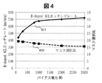
- FIG. 1 is a longitudinal sectional view of a parallel plate type magnetic field VHF dry etching apparatus according to the present invention. It is a figure which shows the etching shape in one Example of the plasma processing method of this invention. It is a schematic diagram of the etching cross section which shows shape abnormality. It is a figure which shows the bias electric power dependence with respect to the B-Doped ACL etching rate and mask selection ratio in this invention. It is a figure which shows the pressure dependence with respect to the B-Doped ACL etching rate and mask selection ratio in this invention.
- FIG. 1 is a longitudinal sectional view of a parallel plate type magnetic field VHF dry etching apparatus which is an example of the plasma processing apparatus of the present invention.
- a sample stage 103 on which a wafer 102 as a sample is placed is provided on the upper surface of a vacuum chamber 101 having a cylindrical inner space and serving as a processing chamber.
- a high frequency power source 105 for bias application and a DC power source 106 for electrostatic chucking of the wafer are connected to the sample stage 103 via a first matching unit 104.
- a temperature control unit 107 is connected to the sample stage 103.
- the high frequency power source 105 uses a frequency of 4 MHz.
- an exhaust port is provided in the lower part of the vacuum vessel 101, and an exhaust device (not shown) is connected to the exhaust port.
- a flat antenna 108 is provided on the upper part of the vacuum chamber 101 so as to face the wafer mounting surface of the sample stage 103, and a high frequency power source 110 for plasma generation is connected via a second matching unit 109. .
- the high frequency power supply 110 uses a VHF wave with a frequency of 200 MHz in this embodiment.
- a solenoid coil 111 for forming a magnetic field in the vacuum vessel 101 is provided on the upper surface and outer periphery outside the vacuum vessel 1. The solenoid coil 111 forms a divergent magnetic field toward the sample stage 103 in the axial direction of the vacuum vessel 101.
- a shower plate 112 having a large number of gas supply holes is provided on the lower surface of the antenna 108 facing the sample stage 103, and an inner space and an outer space surrounding the inner space are formed between the antenna 108 and the shower plate 112.
- the gas supply holes are connected to each space.
- An inner gas supply path 113 is provided in the inner space, and an outer gas supply path 114 is provided in the outer space.
- the main gas system 115 and the inner additive gas system 116 are mixed and connected to the inner gas supply path 113, and the main gas system 115 and the outer additive gas system 117 are mixed and connected to the outer gas supply path 114. is there.
- the main gas system 115 is a gas system of a first gas that is a mixed gas composed of oxygen, a fluorine-containing gas, a halogen gas, and an inert gas.
- the fluorine-containing gas is CHF 3 .
- the halogen gas is Cl 2 and the inert gas is N 2 .
- the main gas line 115 includes a flow controller A118 for controlling the flow rate of the gas source O 2, the flow controller B119 for controlling the flow rate of the gas source CHF 3, a flow controller C120 for controlling the gas source Cl 2 flow rate, a flow controller D121a for controlling the flow rate of the gas source N 2, gas flow divider to these free flow controller 118 and stop valve 123 connected respectively to 121a, gas mixed through a respective stop valve 123 is supplied 124.
- the inner additive gas system 116 and the outer additive gas system 117 are gas systems of a second gas that is a mixed gas composed of a silicon-containing gas (silicon tetrachloride gas or silicon tetrafluoride gas) and an inert gas.
- a silicon-containing gas SiCl 4
- the inert gas is N 2 .
- Stop valve outer additive gas line 117 which are connected respectively with flow controller D121c for controlling the flow rate of the gas source N 2, and the flow controller E122b for controlling the flow rate of the gas source SiCl 4, these flow controllers D121c and 122b 123, and the mixed gas is supplied through the respective stop valves 123.
- Each gas whose gas flow rate from each gas source is adjusted to each set flow rate by the flow rate controllers 118 to 121a is divided into a predetermined ratio by the gas flow rate diverter 115 to the inner gas supply channel 113 and the outer gas supply channel 114. Is washed away.
- Each gas whose gas flow rate from each gas source is adjusted to each set flow rate by the flow rate controllers 121b and 122a is mixed with the gas diverted to the inner gas supply path 113 by the gas flow rate diverter 115 and It is supplied to the inner space and supplied to the central side of the vacuum vessel 101 through the gas supply hole.
- Each gas whose gas flow rate from each gas source is adjusted to each set flow rate by the flow rate controllers 121c and 122b is mixed with the gas diverted to the outer gas supply path 114 by the gas flow rate diverter 115 and It is supplied to the outer space and supplied to the outside surrounding the central portion of the vacuum vessel 101 through the gas supply hole.
- the main gas is divided at a predetermined ratio according to the separated inner and outer regions of the shower plate by the gas flow diverter 124, and the flow rate adjusted additive gas is merged with each main gas divided at the predetermined ratio, Supply to the inner and outer areas of the shower plate.
- the in-plane distribution which adjusted each gas component arbitrarily in the radial direction below the shower plate 112 in the vacuum vessel 101 can be obtained.
- the gas reservoir space in the shower plate 112 is separated into two regions, the inside and outside, but it may be three or more regions, or a plurality of regions may be separated in the circumferential direction, according to the number separated.
- the number of divisions of the gas flow divider 124 may be set, and the number of additive gas systems of the same gas type may be provided.
- a wafer 102 carried into the vacuum vessel 101 by a transfer device (not shown) is placed on the sample stage 103, and the wafer 102 is electrostatically adsorbed on the sample stage 103 by applying a voltage from the DC power source 106.
- the back surface of the wafer 102 adsorbed and held on the sample stage 103 is supplied with H 2 gas, which is a heat transfer gas, and heat is transferred between the temperature of the sample stage 103 adjusted by the temperature control unit 107 and the wafer. 102 is maintained at a predetermined processing temperature.
- flow control is performed in the vacuum vessel 101 from the main gas system 115, the inner additive gas system 116, and the outer additive gas system 117 to the inner gas supply path 113 and the outer gas supply path 114, respectively.
- a mixed gas of O 2 , CHF 3 , Cl 2 , SiCl 4 , and N 2 that is the processed gas is supplied.
- the supplied mixed gas is supplied into the vacuum vessel through the shower plate 112 and is maintained at a predetermined processing pressure in the vacuum vessel 101, and the magnetic field from the solenoid coil 111 together with the high frequency power of 200 MHz from the high frequency power supply 110. As a result, the mixed gas is excited and turned into plasma.
- a high frequency power for bias is supplied to the sample stage 103 by the high frequency power source 105.
- ions in the plasma enter the wafer 2 and the wafer 102 is etched.
- each gas component supplied into the vacuum vessel 101 is arbitrarily adjusted in the radial direction, and in the plasma, radicals and ions of gas components dissociated according to the in-plane distribution are distributed, and the wafer 102 It is adjusted so as to act uniformly on the in-plane etching process.
- the wafer 102 as the material to be etched has a laminated film shown in FIG.
- a pair layer 201 is formed on the wafer substrate, and in this embodiment, a laminated film in which a silicon oxide film (SiO 2) and a polysilicon film (Poly-Si) are alternately laminated is provided.
- a film (B-Doped ACL film) 202, a silicon oxynitride film (SiON) 203, an antireflection film (BARC) 204, and a photoresist film (PR) 205 are provided.
- the pattern is transferred by etching the antireflection film 204 and the silicon oxynitride film 203 using the photoresist film 205 exposed to the circuit pattern as a mask.
- a mixed gas of CHF 3 gas and SF 6 gas is used in the etching process of the silicon oxynitride film 203.
- a treatment for removing the photoresist film 205 and the antireflection film 204 may be added.
- the B-doped ACL 202 is etched using the silicon oxynitride film 203 as a mask.
- the present invention in order to etch boron in the ACL film 202 using the silicon oxynitride film 203 as a mask, in addition to oxygen which is a conventional ACL etchant, fluorine-containing gas, halogen gas, silicon tetrachloride gas (SiCl 4 ), or four A mixed gas of silicon fluoride gas (SiF 4 ) is used.
- the ratio of the halogen gas to the entire gas is appropriately set according to the boron content (for example, 5-70%) contained in the B-Doped ACL 202 and the set temperature of the temperature control unit 107.
- the temperature of the temperature control unit 107 is set to 50 ° C., and a mixed gas of O 2 gas, CHF 3 gas, Cl 2 gas, and SiCl 4 gas. It was used.
- the tendency of each gas type is as follows.
- the temperature of the sample stage 103 is maintained from the upper film of the B-Doped ACL film to the lower film in order to maintain high throughput in the integrated processing from the upper film of the B-Doped ACL film to the lower film. It is preferable to set the temperature difference suitable for etching within ⁇ 10 ° C. (when the change rate between steps is 1 ° C./s, the temperature change waiting time is within 10 s). Further, it is common to change the temperature of the sample stage 103 in accordance with the material change of the upper and lower layers of the B-Doped ACL film.
- the temperature of the sample stage 103 was increased as necessary, and the flow rate ratio of CHF 3 was decreased and increased in each film.
- the flow rate ratio of CHF 3 was decreased and increased in each film.
- the temperature of the sample stage 103 is lowered, side etch can be reduced by reducing the reaction probability of fluorine radicals due to the temperature drop, so the Cl 2 gas ratio to the CHF 3 gas is preferably lowered. That is, the angle of the bowing shape or the taper shape can be adjusted by adjusting the temperature of the sample stage 103.
- a high anisotropic shape can be obtained by setting a high ratio of Cl 2 gas to CHF 3 gas, but by using a high bias power and high pressure region, a high rate equal to or higher than that of conventional ACL etching can be obtained. Processing becomes possible. Further, increasing the bias has the effect of increasing the side wall protection due to the increase of reaction products, and has the effect of suppressing side etching and bowing. Further, as shown in FIG. 4, the etching rate 401 of the B-Doped ACL film greatly increases as the bias power increases in the region where the bias power is 1000 W or less, but gradually increases in the region where the bias power is 1000 W or more.
- the mask selection ratio 402 gradually decreases as the bias power increases, but the reduction range is small. That is, in order to process the B-Doped ACL film at a high etching rate, the power setting of the bias power source is preferably set to 1000 W or more. At this time, at 1000 W of 4 MHz, Vpp, which is the peak-to-peak voltage of the sine wave, is 1350 V. Therefore, when the bias frequency is different, the power can be adjusted by power supply power exceeding Vpp or by direct Vpp control.
- the pressure setting is preferably 4 Pa or higher.
- the silicon oxide compound is deposited on the silicon oxynitride film 203 as a mask by adding silicon tetrachloride gas or silicon tetrafluoride gas, and the etching amount of the silicon oxynitride film 203 is reduced.
- the selection ratio can be increased.
- the retreat of the mask can be reduced, and the faceting 304 at the upper part of the shape is suppressed as shown in FIG.
- the thickness can be as low as a conventional ACL etching process such as ⁇ 40 nm. This avoids complication of the mask film forming process and improves the throughput and CoO.
- the wafer stage may be 100 ° C. or less.
- the temperature is preferably set to 0 ° C. or more and 60 ° C. or less.
- CHF 3 gas is used as the fluorine-containing gas, but other CH 2 F 2 gas, CH 3 F gas, NF 3 gas, CF 4 gas, and SF 6 gas may be used.
- a Br-containing gas such as HBr gas or HI gas may be used.
- SiF 4 gas may be used in addition to SiCl 4 gas.
- NF 3 gas, CF 4 gas, SF 6 gas, or the like that generates a larger amount of fluorine than CHF 3 gas is used, the fluorine-based gas ratio is lowered than when CHF 3 gas is used, or the sample stage 103 The vertical shape can be maintained by lowering the set temperature.
- an amorphous material containing boron using a mixed gas of oxygen gas, fluorine-containing gas, halogen gas, and silicon tetrachloride gas or a mixed gas of oxygen gas, fluorine-containing gas, halogen gas, and silicon tetrafluoride gas was plasma-etched, but a mixed gas of oxygen gas, fluorine-containing gas, halogen gas, and silicon tetrachloride gas or a mixed gas of oxygen gas, fluorine-containing gas, halogen gas, and silicon tetrafluoride gas was N. Even if diluted with an inert gas such as 2 gas, Ar gas, He gas, Xe gas, or Kr gas, the same effect as in this embodiment can be obtained.
- an inert gas such as 2 gas, Ar gas, He gas, Xe gas, or Kr gas
- HBr gas when using HBr gas, it has a low reactivity than Cl 2 gas can be controlled in a small flow rate from Cl 2 gas.
- SiF 4 gas when used, it is an oxide film precursor as well as a fluorine element supply source, so a high selectivity can be realized by adjusting the flow rate appropriately while reducing the amount of fluorine-based gas. .
- the mask formation example of the B-Doped ACL film which is an amorphous carbon film containing boron
- the dry etching according to the present invention was applied to an amorphous carbon film containing no boron.
- the same effect as the present embodiment can be obtained. That is, even if the dry etching according to the present invention is applied to a conventional amorphous carbon film, the same effect as that of the present embodiment can be obtained.
- the main component of the amorphous carbon film containing no boron is the same organic material as the main component of the amorphous carbon film containing boron, and silicon oxide is added by adding silicon tetrachloride gas or silicon tetrafluoride gas. This is because the compound is deposited on the silicon oxynitride film 203 as a mask and the etching amount of the silicon oxynitride film 203 is reduced, thereby improving the selectivity.
- etching apparatus that is equipped with the above-described gas species and can apply a bias of about 3000 W and is uniform at a high pressure of 4 Pa or higher.
- the parallel plate structure VHF etching apparatus shown in FIG. 1 was used.
- CCP capacitively coupled plasma
- ICP inductively coupled plasma
- Micro Wave Electron CyRectron wave etc.
- the same effects as in this embodiment can be obtained by adjusting the pressure, gas flow rate, gas ratio, bias power, frequency, stage temperature, and the like.
- an amorphous carbon film can be etched with a high etching rate and a high selection ratio using an inorganic film as a mask, so that an integrated etching process including pre- and post-processes is possible, and the mask film forming process is simplified. Therefore, it is possible to realize a high throughput including pre- and post-processes.
Landscapes
- Physics & Mathematics (AREA)
- Engineering & Computer Science (AREA)
- Plasma & Fusion (AREA)
- Chemical & Material Sciences (AREA)
- Analytical Chemistry (AREA)
- Electromagnetism (AREA)
- Spectroscopy & Molecular Physics (AREA)
- Drying Of Semiconductors (AREA)
- Plasma Technology (AREA)
Abstract
Description
102:ウェハ
103:試料台
104:第一の整合器
105:バイアス印加用の高周波電源
106:直流電源
107:温調ユニット
108:アンテナ
109:第二の整合器
110:プラズマ生成用の高周波電源
111:ソレノイドコイル
112:シャワープレート
113:内側ガス供給路
114:外側ガス供給路
115:メインガス系統
116:内側添加ガス系統
117:外側添加ガス系統
118:流量制御器A
119:流量制御器B
120:流量制御器C
121a:流量制御器D
121b:流量制御器D
121c:流量制御器D
122a:流量制御器E
122b:流量制御器E
123:ストップバルブ
124:ガス分流器
201:シリコン酸化膜とポリシリコン膜のペア層
202:B-Doped ACL膜
203:シリコン酸窒化膜
204:反射防止膜
205:フォトレジスト膜
301:サイドエッチ
302:ボーイング
303:エッチストップ
304:ファセッティング
Claims (9)
- ホウ素が含有されたアモルファスカーボン膜を有する積層膜をプラズマエッチングすることによりマスクを形成するプラズマ処理方法において、
酸素ガスとフッ素含有ガスとハロゲンガスと四フッ化シリコンガスの混合ガスまたは酸素ガスとフッ素含有ガスとハロゲンガスと四塩化シリコンガスの混合ガスを用いて前記ホウ素が含有されたアモルファスカーボン膜をプラズマエッチングすることを特徴とするプラズマ処理方法。 - 請求項1に記載のプラズマ処理方法において、
前記フッ素含有ガスは、CHF3ガス、CH2F2ガス、CH3Fガス、NF3ガス、CF4ガスまたはSF6ガスであって、
前記ハロゲンガスは、Cl2ガス、HBrガスまたはHIガスであることを特徴とするプラズマ処理方法。 - 請求項1に記載のプラズマ処理方法において、
前記混合ガスに対する前記ハロゲンガスの流量比率は、前記混合ガスに対する前記フッ素含有ガスの流量比率より高いことを特徴とするプラズマ処理方法。 - 請求項1に記載のプラズマ処理方法において、
前記積層膜が成膜された試料を載置する試料台に1000W以上の高周波電力を供給または前記試料台に1350V以上のピーク間高周波電圧を印加することにより前記ホウ素が含有されたアモルファスカーボン膜をプラズマエッチングすることを特徴とするプラズマ処理方法。 - 請求項1ないし請求項4のいずれか一項に記載のプラズマ処理方法において、
圧力を4Pa以上として前記ホウ素が含有されたアモルファスカーボン膜をプラズマエッチングすることを特徴とするプラズマ処理方法。 - 請求項1に記載のプラズマ処理方法において、
O2ガスとCHF3ガスとCl2ガスとSiCl4ガスの混合ガスを用いて前記ホウ素が含有されたアモルファスカーボン膜をプラズマエッチングすることを特徴とするプラズマ処理方法。 - アモルファスカーボン膜を有する積層膜をプラズマエッチングすることによりマスクを形成するプラズマ処理方法において、
酸素ガスとフッ素含有ガスとハロゲンガスと四フッ化シリコンガスの混合ガスまたは酸素ガスとフッ素含有ガスとハロゲンガスと四塩化シリコンガスの混合ガスを用いて前記アモルファスカーボン膜をプラズマエッチングすることを特徴とするプラズマ処理方法。 - 試料がプラズマ処理される処理室と、前記処理室内にプラズマを生成するための高周波電力を供給する高周波電源とを備えるプラズマ処理装置において、
第一のガスと前記第一のガスへ混合されるガスである第二のガスを複数の領域を介して前記処理室内へ供給するガス供給機構をさらに備えることを特徴とするプラズマ処理装置。 - 請求項8に記載のプラズマ処理装置において、
前記ガス供給機構は、複数のガスが混合された第一のガスを前記複数の領域の各々に供給する第一のガス配管と、前記第一のガス配管に接続され前記第二のガスが流れる第二のガス配管とを有することを特徴とするプラズマ処理装置。
Priority Applications (9)
| Application Number | Priority Date | Filing Date | Title |
|---|---|---|---|
| KR1020187015807A KR102262750B1 (ko) | 2016-03-28 | 2017-01-31 | 플라스마 처리 방법 및 플라스마 처리 장치 |
| CN202010515418.1A CN111627807B (zh) | 2016-03-28 | 2017-01-31 | 等离子处理方法以及等离子处理装置 |
| KR1020197029860A KR102329531B1 (ko) | 2016-03-28 | 2017-01-31 | 플라스마 처리 방법 및 플라스마 처리 장치 |
| JP2017538254A JP6458156B2 (ja) | 2016-03-28 | 2017-01-31 | プラズマ処理方法 |
| KR1020177020315A KR101990332B1 (ko) | 2016-03-28 | 2017-01-31 | 플라스마 처리 방법 및 플라스마 처리 장치 |
| US15/558,045 US10157750B2 (en) | 2016-03-28 | 2017-01-31 | Plasma processing method and plasma processing apparatus |
| CN201780000763.8A CN107438892B (zh) | 2016-03-28 | 2017-01-31 | 等离子处理方法以及等离子处理装置 |
| TW106110331A TWI638406B (zh) | 2016-03-28 | 2017-03-28 | 電漿處理方法 |
| TW107121935A TWI685034B (zh) | 2016-03-28 | 2017-03-28 | 電漿處理方法 |
Applications Claiming Priority (2)
| Application Number | Priority Date | Filing Date | Title |
|---|---|---|---|
| JP2016062977 | 2016-03-28 | ||
| JP2016-062977 | 2016-03-28 |
Publications (1)
| Publication Number | Publication Date |
|---|---|
| WO2017154407A1 true WO2017154407A1 (ja) | 2017-09-14 |
Family
ID=59790197
Family Applications (1)
| Application Number | Title | Priority Date | Filing Date |
|---|---|---|---|
| PCT/JP2017/003258 Ceased WO2017154407A1 (ja) | 2016-03-28 | 2017-01-31 | プラズマ処理方法およびプラズマ処理装置 |
Country Status (6)
| Country | Link |
|---|---|
| US (1) | US10157750B2 (ja) |
| JP (3) | JP6458156B2 (ja) |
| KR (3) | KR101990332B1 (ja) |
| CN (2) | CN107438892B (ja) |
| TW (2) | TWI685034B (ja) |
| WO (1) | WO2017154407A1 (ja) |
Cited By (4)
| Publication number | Priority date | Publication date | Assignee | Title |
|---|---|---|---|---|
| KR20190031806A (ko) * | 2017-09-18 | 2019-03-27 | 삼성전자주식회사 | 반도체 장치 및 그 제조 방법 |
| WO2020031224A1 (ja) * | 2018-08-06 | 2020-02-13 | 株式会社日立ハイテクノロジーズ | プラズマ処理方法およびプラズマアッシング装置 |
| JP2021530119A (ja) * | 2018-10-31 | 2021-11-04 | インテグリス・インコーポレーテッド | ホウ素ドープアモルファスカーボンハードマスク及び方法 |
| US11875978B2 (en) | 2020-06-16 | 2024-01-16 | Hitachi High-Tech Corporation | Plasma processing apparatus and plasma processing method |
Families Citing this family (342)
| Publication number | Priority date | Publication date | Assignee | Title |
|---|---|---|---|---|
| US9394608B2 (en) | 2009-04-06 | 2016-07-19 | Asm America, Inc. | Semiconductor processing reactor and components thereof |
| US8802201B2 (en) | 2009-08-14 | 2014-08-12 | Asm America, Inc. | Systems and methods for thin-film deposition of metal oxides using excited nitrogen-oxygen species |
| US9312155B2 (en) | 2011-06-06 | 2016-04-12 | Asm Japan K.K. | High-throughput semiconductor-processing apparatus equipped with multiple dual-chamber modules |
| US10854498B2 (en) | 2011-07-15 | 2020-12-01 | Asm Ip Holding B.V. | Wafer-supporting device and method for producing same |
| US20130023129A1 (en) | 2011-07-20 | 2013-01-24 | Asm America, Inc. | Pressure transmitter for a semiconductor processing environment |
| US9017481B1 (en) | 2011-10-28 | 2015-04-28 | Asm America, Inc. | Process feed management for semiconductor substrate processing |
| US10714315B2 (en) | 2012-10-12 | 2020-07-14 | Asm Ip Holdings B.V. | Semiconductor reaction chamber showerhead |
| US20160376700A1 (en) | 2013-02-01 | 2016-12-29 | Asm Ip Holding B.V. | System for treatment of deposition reactor |
| US10683571B2 (en) | 2014-02-25 | 2020-06-16 | Asm Ip Holding B.V. | Gas supply manifold and method of supplying gases to chamber using same |
| US10167557B2 (en) | 2014-03-18 | 2019-01-01 | Asm Ip Holding B.V. | Gas distribution system, reactor including the system, and methods of using the same |
| US11015245B2 (en) | 2014-03-19 | 2021-05-25 | Asm Ip Holding B.V. | Gas-phase reactor and system having exhaust plenum and components thereof |
| US10858737B2 (en) | 2014-07-28 | 2020-12-08 | Asm Ip Holding B.V. | Showerhead assembly and components thereof |
| US9890456B2 (en) | 2014-08-21 | 2018-02-13 | Asm Ip Holding B.V. | Method and system for in situ formation of gas-phase compounds |
| US9657845B2 (en) | 2014-10-07 | 2017-05-23 | Asm Ip Holding B.V. | Variable conductance gas distribution apparatus and method |
| US10941490B2 (en) | 2014-10-07 | 2021-03-09 | Asm Ip Holding B.V. | Multiple temperature range susceptor, assembly, reactor and system including the susceptor, and methods of using the same |
| US10276355B2 (en) | 2015-03-12 | 2019-04-30 | Asm Ip Holding B.V. | Multi-zone reactor, system including the reactor, and method of using the same |
| US10458018B2 (en) | 2015-06-26 | 2019-10-29 | Asm Ip Holding B.V. | Structures including metal carbide material, devices including the structures, and methods of forming same |
| US10600673B2 (en) | 2015-07-07 | 2020-03-24 | Asm Ip Holding B.V. | Magnetic susceptor to baseplate seal |
| US10211308B2 (en) | 2015-10-21 | 2019-02-19 | Asm Ip Holding B.V. | NbMC layers |
| US11139308B2 (en) | 2015-12-29 | 2021-10-05 | Asm Ip Holding B.V. | Atomic layer deposition of III-V compounds to form V-NAND devices |
| US10529554B2 (en) | 2016-02-19 | 2020-01-07 | Asm Ip Holding B.V. | Method for forming silicon nitride film selectively on sidewalls or flat surfaces of trenches |
| US10343920B2 (en) | 2016-03-18 | 2019-07-09 | Asm Ip Holding B.V. | Aligned carbon nanotubes |
| CN107438892B (zh) * | 2016-03-28 | 2021-08-24 | 株式会社日立高新技术 | 等离子处理方法以及等离子处理装置 |
| US10865475B2 (en) | 2016-04-21 | 2020-12-15 | Asm Ip Holding B.V. | Deposition of metal borides and silicides |
| US10190213B2 (en) | 2016-04-21 | 2019-01-29 | Asm Ip Holding B.V. | Deposition of metal borides |
| US10032628B2 (en) | 2016-05-02 | 2018-07-24 | Asm Ip Holding B.V. | Source/drain performance through conformal solid state doping |
| US10367080B2 (en) | 2016-05-02 | 2019-07-30 | Asm Ip Holding B.V. | Method of forming a germanium oxynitride film |
| US11453943B2 (en) | 2016-05-25 | 2022-09-27 | Asm Ip Holding B.V. | Method for forming carbon-containing silicon/metal oxide or nitride film by ALD using silicon precursor and hydrocarbon precursor |
| US10612137B2 (en) | 2016-07-08 | 2020-04-07 | Asm Ip Holdings B.V. | Organic reactants for atomic layer deposition |
| US9859151B1 (en) | 2016-07-08 | 2018-01-02 | Asm Ip Holding B.V. | Selective film deposition method to form air gaps |
| US10714385B2 (en) | 2016-07-19 | 2020-07-14 | Asm Ip Holding B.V. | Selective deposition of tungsten |
| US9812320B1 (en) | 2016-07-28 | 2017-11-07 | Asm Ip Holding B.V. | Method and apparatus for filling a gap |
| KR102532607B1 (ko) | 2016-07-28 | 2023-05-15 | 에이에스엠 아이피 홀딩 비.브이. | 기판 가공 장치 및 그 동작 방법 |
| US9887082B1 (en) | 2016-07-28 | 2018-02-06 | Asm Ip Holding B.V. | Method and apparatus for filling a gap |
| US10643826B2 (en) | 2016-10-26 | 2020-05-05 | Asm Ip Holdings B.V. | Methods for thermally calibrating reaction chambers |
| US11532757B2 (en) | 2016-10-27 | 2022-12-20 | Asm Ip Holding B.V. | Deposition of charge trapping layers |
| US10714350B2 (en) | 2016-11-01 | 2020-07-14 | ASM IP Holdings, B.V. | Methods for forming a transition metal niobium nitride film on a substrate by atomic layer deposition and related semiconductor device structures |
| US10643904B2 (en) | 2016-11-01 | 2020-05-05 | Asm Ip Holdings B.V. | Methods for forming a semiconductor device and related semiconductor device structures |
| US10229833B2 (en) | 2016-11-01 | 2019-03-12 | Asm Ip Holding B.V. | Methods for forming a transition metal nitride film on a substrate by atomic layer deposition and related semiconductor device structures |
| US10134757B2 (en) | 2016-11-07 | 2018-11-20 | Asm Ip Holding B.V. | Method of processing a substrate and a device manufactured by using the method |
| KR102546317B1 (ko) | 2016-11-15 | 2023-06-21 | 에이에스엠 아이피 홀딩 비.브이. | 기체 공급 유닛 및 이를 포함하는 기판 처리 장치 |
| KR102762543B1 (ko) | 2016-12-14 | 2025-02-05 | 에이에스엠 아이피 홀딩 비.브이. | 기판 처리 장치 |
| US11447861B2 (en) | 2016-12-15 | 2022-09-20 | Asm Ip Holding B.V. | Sequential infiltration synthesis apparatus and a method of forming a patterned structure |
| US11581186B2 (en) | 2016-12-15 | 2023-02-14 | Asm Ip Holding B.V. | Sequential infiltration synthesis apparatus |
| KR102700194B1 (ko) | 2016-12-19 | 2024-08-28 | 에이에스엠 아이피 홀딩 비.브이. | 기판 처리 장치 |
| US10269558B2 (en) | 2016-12-22 | 2019-04-23 | Asm Ip Holding B.V. | Method of forming a structure on a substrate |
| US10867788B2 (en) | 2016-12-28 | 2020-12-15 | Asm Ip Holding B.V. | Method of forming a structure on a substrate |
| US11390950B2 (en) | 2017-01-10 | 2022-07-19 | Asm Ip Holding B.V. | Reactor system and method to reduce residue buildup during a film deposition process |
| US10655221B2 (en) | 2017-02-09 | 2020-05-19 | Asm Ip Holding B.V. | Method for depositing oxide film by thermal ALD and PEALD |
| US10468261B2 (en) | 2017-02-15 | 2019-11-05 | Asm Ip Holding B.V. | Methods for forming a metallic film on a substrate by cyclical deposition and related semiconductor device structures |
| US10529563B2 (en) | 2017-03-29 | 2020-01-07 | Asm Ip Holdings B.V. | Method for forming doped metal oxide films on a substrate by cyclical deposition and related semiconductor device structures |
| USD876504S1 (en) | 2017-04-03 | 2020-02-25 | Asm Ip Holding B.V. | Exhaust flow control ring for semiconductor deposition apparatus |
| KR102457289B1 (ko) | 2017-04-25 | 2022-10-21 | 에이에스엠 아이피 홀딩 비.브이. | 박막 증착 방법 및 반도체 장치의 제조 방법 |
| US10770286B2 (en) | 2017-05-08 | 2020-09-08 | Asm Ip Holdings B.V. | Methods for selectively forming a silicon nitride film on a substrate and related semiconductor device structures |
| US10892156B2 (en) | 2017-05-08 | 2021-01-12 | Asm Ip Holding B.V. | Methods for forming a silicon nitride film on a substrate and related semiconductor device structures |
| US12040200B2 (en) | 2017-06-20 | 2024-07-16 | Asm Ip Holding B.V. | Semiconductor processing apparatus and methods for calibrating a semiconductor processing apparatus |
| US11306395B2 (en) | 2017-06-28 | 2022-04-19 | Asm Ip Holding B.V. | Methods for depositing a transition metal nitride film on a substrate by atomic layer deposition and related deposition apparatus |
| US10685834B2 (en) | 2017-07-05 | 2020-06-16 | Asm Ip Holdings B.V. | Methods for forming a silicon germanium tin layer and related semiconductor device structures |
| KR20190009245A (ko) | 2017-07-18 | 2019-01-28 | 에이에스엠 아이피 홀딩 비.브이. | 반도체 소자 구조물 형성 방법 및 관련된 반도체 소자 구조물 |
| US10541333B2 (en) | 2017-07-19 | 2020-01-21 | Asm Ip Holding B.V. | Method for depositing a group IV semiconductor and related semiconductor device structures |
| US11018002B2 (en) | 2017-07-19 | 2021-05-25 | Asm Ip Holding B.V. | Method for selectively depositing a Group IV semiconductor and related semiconductor device structures |
| US11374112B2 (en) | 2017-07-19 | 2022-06-28 | Asm Ip Holding B.V. | Method for depositing a group IV semiconductor and related semiconductor device structures |
| US10590535B2 (en) | 2017-07-26 | 2020-03-17 | Asm Ip Holdings B.V. | Chemical treatment, deposition and/or infiltration apparatus and method for using the same |
| TWI815813B (zh) | 2017-08-04 | 2023-09-21 | 荷蘭商Asm智慧財產控股公司 | 用於分配反應腔內氣體的噴頭總成 |
| US10692741B2 (en) | 2017-08-08 | 2020-06-23 | Asm Ip Holdings B.V. | Radiation shield |
| US10770336B2 (en) | 2017-08-08 | 2020-09-08 | Asm Ip Holding B.V. | Substrate lift mechanism and reactor including same |
| US10249524B2 (en) | 2017-08-09 | 2019-04-02 | Asm Ip Holding B.V. | Cassette holder assembly for a substrate cassette and holding member for use in such assembly |
| US11769682B2 (en) | 2017-08-09 | 2023-09-26 | Asm Ip Holding B.V. | Storage apparatus for storing cassettes for substrates and processing apparatus equipped therewith |
| US11139191B2 (en) | 2017-08-09 | 2021-10-05 | Asm Ip Holding B.V. | Storage apparatus for storing cassettes for substrates and processing apparatus equipped therewith |
| USD900036S1 (en) | 2017-08-24 | 2020-10-27 | Asm Ip Holding B.V. | Heater electrical connector and adapter |
| US11830730B2 (en) | 2017-08-29 | 2023-11-28 | Asm Ip Holding B.V. | Layer forming method and apparatus |
| KR102491945B1 (ko) | 2017-08-30 | 2023-01-26 | 에이에스엠 아이피 홀딩 비.브이. | 기판 처리 장치 |
| US11056344B2 (en) | 2017-08-30 | 2021-07-06 | Asm Ip Holding B.V. | Layer forming method |
| US11295980B2 (en) | 2017-08-30 | 2022-04-05 | Asm Ip Holding B.V. | Methods for depositing a molybdenum metal film over a dielectric surface of a substrate by a cyclical deposition process and related semiconductor device structures |
| KR102401446B1 (ko) | 2017-08-31 | 2022-05-24 | 에이에스엠 아이피 홀딩 비.브이. | 기판 처리 장치 |
| JP6814116B2 (ja) * | 2017-09-13 | 2021-01-13 | キオクシア株式会社 | 半導体装置の製造方法および半導体製造装置 |
| KR102630301B1 (ko) | 2017-09-21 | 2024-01-29 | 에이에스엠 아이피 홀딩 비.브이. | 침투성 재료의 순차 침투 합성 방법 처리 및 이를 이용하여 형성된 구조물 및 장치 |
| US10844484B2 (en) | 2017-09-22 | 2020-11-24 | Asm Ip Holding B.V. | Apparatus for dispensing a vapor phase reactant to a reaction chamber and related methods |
| US10658205B2 (en) | 2017-09-28 | 2020-05-19 | Asm Ip Holdings B.V. | Chemical dispensing apparatus and methods for dispensing a chemical to a reaction chamber |
| US10403504B2 (en) | 2017-10-05 | 2019-09-03 | Asm Ip Holding B.V. | Method for selectively depositing a metallic film on a substrate |
| US10319588B2 (en) | 2017-10-10 | 2019-06-11 | Asm Ip Holding B.V. | Method for depositing a metal chalcogenide on a substrate by cyclical deposition |
| US10923344B2 (en) | 2017-10-30 | 2021-02-16 | Asm Ip Holding B.V. | Methods for forming a semiconductor structure and related semiconductor structures |
| KR102443047B1 (ko) | 2017-11-16 | 2022-09-14 | 에이에스엠 아이피 홀딩 비.브이. | 기판 처리 장치 방법 및 그에 의해 제조된 장치 |
| US10910262B2 (en) | 2017-11-16 | 2021-02-02 | Asm Ip Holding B.V. | Method of selectively depositing a capping layer structure on a semiconductor device structure |
| US11022879B2 (en) | 2017-11-24 | 2021-06-01 | Asm Ip Holding B.V. | Method of forming an enhanced unexposed photoresist layer |
| JP7214724B2 (ja) | 2017-11-27 | 2023-01-30 | エーエスエム アイピー ホールディング ビー.ブイ. | バッチ炉で利用されるウェハカセットを収納するための収納装置 |
| TWI791689B (zh) | 2017-11-27 | 2023-02-11 | 荷蘭商Asm智慧財產控股私人有限公司 | 包括潔淨迷你環境之裝置 |
| US11127599B2 (en) * | 2018-01-12 | 2021-09-21 | Applied Materials, Inc. | Methods for etching a hardmask layer |
| US10872771B2 (en) | 2018-01-16 | 2020-12-22 | Asm Ip Holding B. V. | Method for depositing a material film on a substrate within a reaction chamber by a cyclical deposition process and related device structures |
| KR102695659B1 (ko) | 2018-01-19 | 2024-08-14 | 에이에스엠 아이피 홀딩 비.브이. | 플라즈마 보조 증착에 의해 갭 충진 층을 증착하는 방법 |
| TWI799494B (zh) | 2018-01-19 | 2023-04-21 | 荷蘭商Asm 智慧財產控股公司 | 沈積方法 |
| USD903477S1 (en) | 2018-01-24 | 2020-12-01 | Asm Ip Holdings B.V. | Metal clamp |
| US11018047B2 (en) | 2018-01-25 | 2021-05-25 | Asm Ip Holding B.V. | Hybrid lift pin |
| USD880437S1 (en) | 2018-02-01 | 2020-04-07 | Asm Ip Holding B.V. | Gas supply plate for semiconductor manufacturing apparatus |
| US11081345B2 (en) | 2018-02-06 | 2021-08-03 | Asm Ip Holding B.V. | Method of post-deposition treatment for silicon oxide film |
| US11685991B2 (en) | 2018-02-14 | 2023-06-27 | Asm Ip Holding B.V. | Method for depositing a ruthenium-containing film on a substrate by a cyclical deposition process |
| US10896820B2 (en) | 2018-02-14 | 2021-01-19 | Asm Ip Holding B.V. | Method for depositing a ruthenium-containing film on a substrate by a cyclical deposition process |
| US10731249B2 (en) | 2018-02-15 | 2020-08-04 | Asm Ip Holding B.V. | Method of forming a transition metal containing film on a substrate by a cyclical deposition process, a method for supplying a transition metal halide compound to a reaction chamber, and related vapor deposition apparatus |
| KR102636427B1 (ko) * | 2018-02-20 | 2024-02-13 | 에이에스엠 아이피 홀딩 비.브이. | 기판 처리 방법 및 장치 |
| US10658181B2 (en) | 2018-02-20 | 2020-05-19 | Asm Ip Holding B.V. | Method of spacer-defined direct patterning in semiconductor fabrication |
| US10975470B2 (en) | 2018-02-23 | 2021-04-13 | Asm Ip Holding B.V. | Apparatus for detecting or monitoring for a chemical precursor in a high temperature environment |
| US11473195B2 (en) | 2018-03-01 | 2022-10-18 | Asm Ip Holding B.V. | Semiconductor processing apparatus and a method for processing a substrate |
| US11629406B2 (en) | 2018-03-09 | 2023-04-18 | Asm Ip Holding B.V. | Semiconductor processing apparatus comprising one or more pyrometers for measuring a temperature of a substrate during transfer of the substrate |
| US11114283B2 (en) | 2018-03-16 | 2021-09-07 | Asm Ip Holding B.V. | Reactor, system including the reactor, and methods of manufacturing and using same |
| KR102646467B1 (ko) | 2018-03-27 | 2024-03-11 | 에이에스엠 아이피 홀딩 비.브이. | 기판 상에 전극을 형성하는 방법 및 전극을 포함하는 반도체 소자 구조 |
| US11088002B2 (en) | 2018-03-29 | 2021-08-10 | Asm Ip Holding B.V. | Substrate rack and a substrate processing system and method |
| US11230766B2 (en) | 2018-03-29 | 2022-01-25 | Asm Ip Holding B.V. | Substrate processing apparatus and method |
| KR102501472B1 (ko) | 2018-03-30 | 2023-02-20 | 에이에스엠 아이피 홀딩 비.브이. | 기판 처리 방법 |
| KR102600229B1 (ko) | 2018-04-09 | 2023-11-10 | 에이에스엠 아이피 홀딩 비.브이. | 기판 지지 장치, 이를 포함하는 기판 처리 장치 및 기판 처리 방법 |
| US12025484B2 (en) | 2018-05-08 | 2024-07-02 | Asm Ip Holding B.V. | Thin film forming method |
| TWI843623B (zh) | 2018-05-08 | 2024-05-21 | 荷蘭商Asm Ip私人控股有限公司 | 藉由循環沉積製程於基板上沉積氧化物膜之方法及相關裝置結構 |
| US12272527B2 (en) | 2018-05-09 | 2025-04-08 | Asm Ip Holding B.V. | Apparatus for use with hydrogen radicals and method of using same |
| KR20190129718A (ko) | 2018-05-11 | 2019-11-20 | 에이에스엠 아이피 홀딩 비.브이. | 기판 상에 피도핑 금속 탄화물 막을 형성하는 방법 및 관련 반도체 소자 구조 |
| KR102596988B1 (ko) | 2018-05-28 | 2023-10-31 | 에이에스엠 아이피 홀딩 비.브이. | 기판 처리 방법 및 그에 의해 제조된 장치 |
| US11718913B2 (en) | 2018-06-04 | 2023-08-08 | Asm Ip Holding B.V. | Gas distribution system and reactor system including same |
| US11270889B2 (en) * | 2018-06-04 | 2022-03-08 | Tokyo Electron Limited | Etching method and etching apparatus |
| TWI840362B (zh) | 2018-06-04 | 2024-05-01 | 荷蘭商Asm Ip私人控股有限公司 | 水氣降低的晶圓處置腔室 |
| CN110571138A (zh) * | 2018-06-05 | 2019-12-13 | 中芯国际集成电路制造(上海)有限公司 | 半导体器件的制作方法 |
| US11286562B2 (en) | 2018-06-08 | 2022-03-29 | Asm Ip Holding B.V. | Gas-phase chemical reactor and method of using same |
| US10797133B2 (en) | 2018-06-21 | 2020-10-06 | Asm Ip Holding B.V. | Method for depositing a phosphorus doped silicon arsenide film and related semiconductor device structures |
| KR102568797B1 (ko) | 2018-06-21 | 2023-08-21 | 에이에스엠 아이피 홀딩 비.브이. | 기판 처리 시스템 |
| TWI871083B (zh) | 2018-06-27 | 2025-01-21 | 荷蘭商Asm Ip私人控股有限公司 | 用於形成含金屬材料之循環沉積製程 |
| US11499222B2 (en) | 2018-06-27 | 2022-11-15 | Asm Ip Holding B.V. | Cyclic deposition methods for forming metal-containing material and films and structures including the metal-containing material |
| US10612136B2 (en) | 2018-06-29 | 2020-04-07 | ASM IP Holding, B.V. | Temperature-controlled flange and reactor system including same |
| KR102686758B1 (ko) | 2018-06-29 | 2024-07-18 | 에이에스엠 아이피 홀딩 비.브이. | 박막 증착 방법 및 반도체 장치의 제조 방법 |
| US10755922B2 (en) | 2018-07-03 | 2020-08-25 | Asm Ip Holding B.V. | Method for depositing silicon-free carbon-containing film as gap-fill layer by pulse plasma-assisted deposition |
| US10388513B1 (en) | 2018-07-03 | 2019-08-20 | Asm Ip Holding B.V. | Method for depositing silicon-free carbon-containing film as gap-fill layer by pulse plasma-assisted deposition |
| US10767789B2 (en) | 2018-07-16 | 2020-09-08 | Asm Ip Holding B.V. | Diaphragm valves, valve components, and methods for forming valve components |
| US11053591B2 (en) | 2018-08-06 | 2021-07-06 | Asm Ip Holding B.V. | Multi-port gas injection system and reactor system including same |
| JP7203531B2 (ja) * | 2018-08-08 | 2023-01-13 | 東京エレクトロン株式会社 | プラズマ処理方法及びプラズマ処理装置 |
| US10883175B2 (en) | 2018-08-09 | 2021-01-05 | Asm Ip Holding B.V. | Vertical furnace for processing substrates and a liner for use therein |
| US10829852B2 (en) | 2018-08-16 | 2020-11-10 | Asm Ip Holding B.V. | Gas distribution device for a wafer processing apparatus |
| US11430674B2 (en) | 2018-08-22 | 2022-08-30 | Asm Ip Holding B.V. | Sensor array, apparatus for dispensing a vapor phase reactant to a reaction chamber and related methods |
| US11024523B2 (en) | 2018-09-11 | 2021-06-01 | Asm Ip Holding B.V. | Substrate processing apparatus and method |
| KR102707956B1 (ko) | 2018-09-11 | 2024-09-19 | 에이에스엠 아이피 홀딩 비.브이. | 박막 증착 방법 |
| US11049751B2 (en) | 2018-09-14 | 2021-06-29 | Asm Ip Holding B.V. | Cassette supply system to store and handle cassettes and processing apparatus equipped therewith |
| CN110970344B (zh) | 2018-10-01 | 2024-10-25 | Asmip控股有限公司 | 衬底保持设备、包含所述设备的系统及其使用方法 |
| US11232963B2 (en) | 2018-10-03 | 2022-01-25 | Asm Ip Holding B.V. | Substrate processing apparatus and method |
| KR102592699B1 (ko) | 2018-10-08 | 2023-10-23 | 에이에스엠 아이피 홀딩 비.브이. | 기판 지지 유닛 및 이를 포함하는 박막 증착 장치와 기판 처리 장치 |
| US10847365B2 (en) | 2018-10-11 | 2020-11-24 | Asm Ip Holding B.V. | Method of forming conformal silicon carbide film by cyclic CVD |
| US10811256B2 (en) | 2018-10-16 | 2020-10-20 | Asm Ip Holding B.V. | Method for etching a carbon-containing feature |
| KR102605121B1 (ko) | 2018-10-19 | 2023-11-23 | 에이에스엠 아이피 홀딩 비.브이. | 기판 처리 장치 및 기판 처리 방법 |
| KR102546322B1 (ko) | 2018-10-19 | 2023-06-21 | 에이에스엠 아이피 홀딩 비.브이. | 기판 처리 장치 및 기판 처리 방법 |
| USD948463S1 (en) | 2018-10-24 | 2022-04-12 | Asm Ip Holding B.V. | Susceptor for semiconductor substrate supporting apparatus |
| US12378665B2 (en) | 2018-10-26 | 2025-08-05 | Asm Ip Holding B.V. | High temperature coatings for a preclean and etch apparatus and related methods |
| US11087997B2 (en) | 2018-10-31 | 2021-08-10 | Asm Ip Holding B.V. | Substrate processing apparatus for processing substrates |
| KR102748291B1 (ko) | 2018-11-02 | 2024-12-31 | 에이에스엠 아이피 홀딩 비.브이. | 기판 지지 유닛 및 이를 포함하는 기판 처리 장치 |
| US11572620B2 (en) | 2018-11-06 | 2023-02-07 | Asm Ip Holding B.V. | Methods for selectively depositing an amorphous silicon film on a substrate |
| US11031242B2 (en) | 2018-11-07 | 2021-06-08 | Asm Ip Holding B.V. | Methods for depositing a boron doped silicon germanium film |
| US10847366B2 (en) | 2018-11-16 | 2020-11-24 | Asm Ip Holding B.V. | Methods for depositing a transition metal chalcogenide film on a substrate by a cyclical deposition process |
| US10818758B2 (en) | 2018-11-16 | 2020-10-27 | Asm Ip Holding B.V. | Methods for forming a metal silicate film on a substrate in a reaction chamber and related semiconductor device structures |
| US10559458B1 (en) | 2018-11-26 | 2020-02-11 | Asm Ip Holding B.V. | Method of forming oxynitride film |
| US12040199B2 (en) | 2018-11-28 | 2024-07-16 | Asm Ip Holding B.V. | Substrate processing apparatus for processing substrates |
| US11217444B2 (en) | 2018-11-30 | 2022-01-04 | Asm Ip Holding B.V. | Method for forming an ultraviolet radiation responsive metal oxide-containing film |
| KR102636428B1 (ko) | 2018-12-04 | 2024-02-13 | 에이에스엠 아이피 홀딩 비.브이. | 기판 처리 장치를 세정하는 방법 |
| US11158513B2 (en) | 2018-12-13 | 2021-10-26 | Asm Ip Holding B.V. | Methods for forming a rhenium-containing film on a substrate by a cyclical deposition process and related semiconductor device structures |
| JP7504584B2 (ja) | 2018-12-14 | 2024-06-24 | エーエスエム・アイピー・ホールディング・ベー・フェー | 窒化ガリウムの選択的堆積を用いてデバイス構造体を形成する方法及びそのためのシステム |
| TWI866480B (zh) | 2019-01-17 | 2024-12-11 | 荷蘭商Asm Ip 私人控股有限公司 | 藉由循環沈積製程於基板上形成含過渡金屬膜之方法 |
| KR102727227B1 (ko) | 2019-01-22 | 2024-11-07 | 에이에스엠 아이피 홀딩 비.브이. | 기판 처리 장치 |
| CN111524788B (zh) | 2019-02-01 | 2023-11-24 | Asm Ip私人控股有限公司 | 氧化硅的拓扑选择性膜形成的方法 |
| TWI845607B (zh) | 2019-02-20 | 2024-06-21 | 荷蘭商Asm Ip私人控股有限公司 | 用來填充形成於基材表面內之凹部的循環沉積方法及設備 |
| KR102626263B1 (ko) | 2019-02-20 | 2024-01-16 | 에이에스엠 아이피 홀딩 비.브이. | 처리 단계를 포함하는 주기적 증착 방법 및 이를 위한 장치 |
| TWI873122B (zh) | 2019-02-20 | 2025-02-21 | 荷蘭商Asm Ip私人控股有限公司 | 填充一基板之一表面內所形成的一凹槽的方法、根據其所形成之半導體結構、及半導體處理設備 |
| KR20200102357A (ko) | 2019-02-20 | 2020-08-31 | 에이에스엠 아이피 홀딩 비.브이. | 3-d nand 응용의 플러그 충진체 증착용 장치 및 방법 |
| TWI842826B (zh) | 2019-02-22 | 2024-05-21 | 荷蘭商Asm Ip私人控股有限公司 | 基材處理設備及處理基材之方法 |
| KR102858005B1 (ko) | 2019-03-08 | 2025-09-09 | 에이에스엠 아이피 홀딩 비.브이. | 실리콘 질화물 층을 선택적으로 증착하는 방법, 및 선택적으로 증착된 실리콘 질화물 층을 포함하는 구조체 |
| KR102762833B1 (ko) | 2019-03-08 | 2025-02-04 | 에이에스엠 아이피 홀딩 비.브이. | SiOCN 층을 포함한 구조체 및 이의 형성 방법 |
| KR102782593B1 (ko) | 2019-03-08 | 2025-03-14 | 에이에스엠 아이피 홀딩 비.브이. | SiOC 층을 포함한 구조체 및 이의 형성 방법 |
| JP2020167398A (ja) | 2019-03-28 | 2020-10-08 | エーエスエム・アイピー・ホールディング・ベー・フェー | ドアオープナーおよびドアオープナーが提供される基材処理装置 |
| KR102809999B1 (ko) | 2019-04-01 | 2025-05-19 | 에이에스엠 아이피 홀딩 비.브이. | 반도체 소자를 제조하는 방법 |
| KR102897355B1 (ko) | 2019-04-19 | 2025-12-08 | 에이에스엠 아이피 홀딩 비.브이. | 층 형성 방법 및 장치 |
| JP6959999B2 (ja) * | 2019-04-19 | 2021-11-05 | 株式会社日立ハイテク | プラズマ処理方法 |
| JP6963097B2 (ja) * | 2019-04-22 | 2021-11-05 | 株式会社日立ハイテク | プラズマ処理方法 |
| KR20200125453A (ko) | 2019-04-24 | 2020-11-04 | 에이에스엠 아이피 홀딩 비.브이. | 기상 반응기 시스템 및 이를 사용하는 방법 |
| KR102929471B1 (ko) | 2019-05-07 | 2026-02-20 | 에이에스엠 아이피 홀딩 비.브이. | 딥 튜브가 있는 화학물질 공급원 용기 |
| KR102869364B1 (ko) | 2019-05-07 | 2025-10-10 | 에이에스엠 아이피 홀딩 비.브이. | 비정질 탄소 중합체 막을 개질하는 방법 |
| KR102929472B1 (ko) | 2019-05-10 | 2026-02-20 | 에이에스엠 아이피 홀딩 비.브이. | 표면 상에 재료를 증착하는 방법 및 본 방법에 따라 형성된 구조 |
| JP7612342B2 (ja) | 2019-05-16 | 2025-01-14 | エーエスエム・アイピー・ホールディング・ベー・フェー | ウェハボートハンドリング装置、縦型バッチ炉および方法 |
| JP7598201B2 (ja) | 2019-05-16 | 2024-12-11 | エーエスエム・アイピー・ホールディング・ベー・フェー | ウェハボートハンドリング装置、縦型バッチ炉および方法 |
| USD947913S1 (en) | 2019-05-17 | 2022-04-05 | Asm Ip Holding B.V. | Susceptor shaft |
| USD975665S1 (en) | 2019-05-17 | 2023-01-17 | Asm Ip Holding B.V. | Susceptor shaft |
| USD935572S1 (en) | 2019-05-24 | 2021-11-09 | Asm Ip Holding B.V. | Gas channel plate |
| USD922229S1 (en) | 2019-06-05 | 2021-06-15 | Asm Ip Holding B.V. | Device for controlling a temperature of a gas supply unit |
| KR20200141002A (ko) | 2019-06-06 | 2020-12-17 | 에이에스엠 아이피 홀딩 비.브이. | 배기 가스 분석을 포함한 기상 반응기 시스템을 사용하는 방법 |
| KR102918757B1 (ko) | 2019-06-10 | 2026-01-28 | 에이에스엠 아이피 홀딩 비.브이. | 석영 에피택셜 챔버를 세정하는 방법 |
| KR20200143254A (ko) | 2019-06-11 | 2020-12-23 | 에이에스엠 아이피 홀딩 비.브이. | 개질 가스를 사용하여 전자 구조를 형성하는 방법, 상기 방법을 수행하기 위한 시스템, 및 상기 방법을 사용하여 형성되는 구조 |
| USD944946S1 (en) | 2019-06-14 | 2022-03-01 | Asm Ip Holding B.V. | Shower plate |
| USD931978S1 (en) | 2019-06-27 | 2021-09-28 | Asm Ip Holding B.V. | Showerhead vacuum transport |
| KR102911421B1 (ko) | 2019-07-03 | 2026-01-12 | 에이에스엠 아이피 홀딩 비.브이. | 기판 처리 장치용 온도 제어 조립체 및 이를 사용하는 방법 |
| JP7499079B2 (ja) | 2019-07-09 | 2024-06-13 | エーエスエム・アイピー・ホールディング・ベー・フェー | 同軸導波管を用いたプラズマ装置、基板処理方法 |
| CN112216646B (zh) | 2019-07-10 | 2026-02-10 | Asmip私人控股有限公司 | 基板支撑组件及包括其的基板处理装置 |
| KR102895115B1 (ko) | 2019-07-16 | 2025-12-03 | 에이에스엠 아이피 홀딩 비.브이. | 기판 처리 장치 |
| TWI826704B (zh) | 2019-07-17 | 2023-12-21 | 荷蘭商Asm Ip私人控股有限公司 | 自由基輔助引燃電漿系統和方法 |
| KR102860110B1 (ko) | 2019-07-17 | 2025-09-16 | 에이에스엠 아이피 홀딩 비.브이. | 실리콘 게르마늄 구조를 형성하는 방법 |
| US11643724B2 (en) | 2019-07-18 | 2023-05-09 | Asm Ip Holding B.V. | Method of forming structures using a neutral beam |
| KR102903090B1 (ko) | 2019-07-19 | 2025-12-19 | 에이에스엠 아이피 홀딩 비.브이. | 토폴로지-제어된 비정질 탄소 중합체 막을 형성하는 방법 |
| TWI839544B (zh) | 2019-07-19 | 2024-04-21 | 荷蘭商Asm Ip私人控股有限公司 | 形成形貌受控的非晶碳聚合物膜之方法 |
| CN112309843B (zh) | 2019-07-29 | 2026-01-23 | Asmip私人控股有限公司 | 实现高掺杂剂掺入的选择性沉积方法 |
| KR20210015655A (ko) | 2019-07-30 | 2021-02-10 | 에이에스엠 아이피 홀딩 비.브이. | 기판 처리 장치 및 방법 |
| CN112309899B (zh) | 2019-07-30 | 2025-11-14 | Asmip私人控股有限公司 | 基板处理设备 |
| CN112309900B (zh) | 2019-07-30 | 2025-11-04 | Asmip私人控股有限公司 | 基板处理设备 |
| US11587814B2 (en) | 2019-07-31 | 2023-02-21 | Asm Ip Holding B.V. | Vertical batch furnace assembly |
| US11587815B2 (en) | 2019-07-31 | 2023-02-21 | Asm Ip Holding B.V. | Vertical batch furnace assembly |
| US11227782B2 (en) | 2019-07-31 | 2022-01-18 | Asm Ip Holding B.V. | Vertical batch furnace assembly |
| KR20210018759A (ko) | 2019-08-05 | 2021-02-18 | 에이에스엠 아이피 홀딩 비.브이. | 화학물질 공급원 용기를 위한 액체 레벨 센서 |
| KR20210018761A (ko) | 2019-08-09 | 2021-02-18 | 에이에스엠 아이피 홀딩 비.브이. | 냉각 장치를 포함한 히터 어셈블리 및 이를 사용하는 방법 |
| USD965044S1 (en) | 2019-08-19 | 2022-09-27 | Asm Ip Holding B.V. | Susceptor shaft |
| USD965524S1 (en) | 2019-08-19 | 2022-10-04 | Asm Ip Holding B.V. | Susceptor support |
| JP7810514B2 (ja) | 2019-08-21 | 2026-02-03 | エーエスエム・アイピー・ホールディング・ベー・フェー | 成膜原料混合ガス生成装置及び成膜装置 |
| JP7190988B2 (ja) * | 2019-08-21 | 2022-12-16 | 東京エレクトロン株式会社 | エッチング方法及び基板処理装置 |
| KR20210024423A (ko) | 2019-08-22 | 2021-03-05 | 에이에스엠 아이피 홀딩 비.브이. | 홀을 구비한 구조체를 형성하기 위한 방법 |
| USD940837S1 (en) | 2019-08-22 | 2022-01-11 | Asm Ip Holding B.V. | Electrode |
| USD949319S1 (en) | 2019-08-22 | 2022-04-19 | Asm Ip Holding B.V. | Exhaust duct |
| USD979506S1 (en) | 2019-08-22 | 2023-02-28 | Asm Ip Holding B.V. | Insulator |
| USD930782S1 (en) | 2019-08-22 | 2021-09-14 | Asm Ip Holding B.V. | Gas distributor |
| US11286558B2 (en) | 2019-08-23 | 2022-03-29 | Asm Ip Holding B.V. | Methods for depositing a molybdenum nitride film on a surface of a substrate by a cyclical deposition process and related semiconductor device structures including a molybdenum nitride film |
| KR102928101B1 (ko) | 2019-08-23 | 2026-02-13 | 에이에스엠 아이피 홀딩 비.브이. | 비스(디에틸아미노)실란을 사용하여 peald에 의해 개선된 품질을 갖는 실리콘 산화물 막을 증착하기 위한 방법 |
| KR102868968B1 (ko) | 2019-09-03 | 2025-10-10 | 에이에스엠 아이피 홀딩 비.브이. | 칼코지나이드 막 및 상기 막을 포함한 구조체를 증착하기 위한 방법 및 장치 |
| KR102806450B1 (ko) | 2019-09-04 | 2025-05-12 | 에이에스엠 아이피 홀딩 비.브이. | 희생 캡핑 층을 이용한 선택적 증착 방법 |
| KR102733104B1 (ko) | 2019-09-05 | 2024-11-22 | 에이에스엠 아이피 홀딩 비.브이. | 기판 처리 장치 |
| WO2021048995A1 (ja) * | 2019-09-13 | 2021-03-18 | 株式会社日立ハイテク | 半導体装置の製造方法及びプラズマ処理装置 |
| US12469693B2 (en) | 2019-09-17 | 2025-11-11 | Asm Ip Holding B.V. | Method of forming a carbon-containing layer and structure including the layer |
| US11562901B2 (en) | 2019-09-25 | 2023-01-24 | Asm Ip Holding B.V. | Substrate processing method |
| CN112593212B (zh) | 2019-10-02 | 2023-12-22 | Asm Ip私人控股有限公司 | 通过循环等离子体增强沉积工艺形成拓扑选择性氧化硅膜的方法 |
| TW202128273A (zh) | 2019-10-08 | 2021-08-01 | 荷蘭商Asm Ip私人控股有限公司 | 氣體注入系統、及將材料沉積於反應室內之基板表面上的方法 |
| KR102948143B1 (ko) | 2019-10-08 | 2026-04-07 | 에이에스엠 아이피 홀딩 비.브이. | 활성 종을 이용하기 위한 가스 분배 어셈블리를 포함한 반응기 시스템 및 이를 사용하는 방법 |
| TWI846953B (zh) | 2019-10-08 | 2024-07-01 | 荷蘭商Asm Ip私人控股有限公司 | 基板處理裝置 |
| TWI846966B (zh) | 2019-10-10 | 2024-07-01 | 荷蘭商Asm Ip私人控股有限公司 | 形成光阻底層之方法及包括光阻底層之結構 |
| US12009241B2 (en) | 2019-10-14 | 2024-06-11 | Asm Ip Holding B.V. | Vertical batch furnace assembly with detector to detect cassette |
| TWI834919B (zh) | 2019-10-16 | 2024-03-11 | 荷蘭商Asm Ip私人控股有限公司 | 氧化矽之拓撲選擇性膜形成之方法 |
| US11637014B2 (en) | 2019-10-17 | 2023-04-25 | Asm Ip Holding B.V. | Methods for selective deposition of doped semiconductor material |
| KR102845724B1 (ko) | 2019-10-21 | 2025-08-13 | 에이에스엠 아이피 홀딩 비.브이. | 막을 선택적으로 에칭하기 위한 장치 및 방법 |
| US11996292B2 (en) | 2019-10-25 | 2024-05-28 | Asm Ip Holding B.V. | Methods for filling a gap feature on a substrate surface and related semiconductor structures |
| US11646205B2 (en) | 2019-10-29 | 2023-05-09 | Asm Ip Holding B.V. | Methods of selectively forming n-type doped material on a surface, systems for selectively forming n-type doped material, and structures formed using same |
| KR102890638B1 (ko) | 2019-11-05 | 2025-11-25 | 에이에스엠 아이피 홀딩 비.브이. | 도핑된 반도체 층을 갖는 구조체 및 이를 형성하기 위한 방법 및 시스템 |
| US11501968B2 (en) | 2019-11-15 | 2022-11-15 | Asm Ip Holding B.V. | Method for providing a semiconductor device with silicon filled gaps |
| KR102861314B1 (ko) | 2019-11-20 | 2025-09-17 | 에이에스엠 아이피 홀딩 비.브이. | 기판의 표면 상에 탄소 함유 물질을 증착하는 방법, 상기 방법을 사용하여 형성된 구조물, 및 상기 구조물을 형성하기 위한 시스템 |
| KR20210065848A (ko) | 2019-11-26 | 2021-06-04 | 에이에스엠 아이피 홀딩 비.브이. | 제1 유전체 표면과 제2 금속성 표면을 포함한 기판 상에 타겟 막을 선택적으로 형성하기 위한 방법 |
| CN112951697B (zh) | 2019-11-26 | 2025-07-29 | Asmip私人控股有限公司 | 基板处理设备 |
| CN120432376A (zh) | 2019-11-29 | 2025-08-05 | Asm Ip私人控股有限公司 | 基板处理设备 |
| CN112885692B (zh) | 2019-11-29 | 2025-08-15 | Asmip私人控股有限公司 | 基板处理设备 |
| JP7527928B2 (ja) | 2019-12-02 | 2024-08-05 | エーエスエム・アイピー・ホールディング・ベー・フェー | 基板処理装置、基板処理方法 |
| KR20210070898A (ko) | 2019-12-04 | 2021-06-15 | 에이에스엠 아이피 홀딩 비.브이. | 기판 처리 장치 |
| US11885013B2 (en) | 2019-12-17 | 2024-01-30 | Asm Ip Holding B.V. | Method of forming vanadium nitride layer and structure including the vanadium nitride layer |
| KR102943768B1 (ko) | 2019-12-19 | 2026-03-26 | 에이에스엠 아이피 홀딩 비.브이. | 기판 상의 갭 피처를 충진하는 방법 및 이와 관련된 반도체 소자 구조 |
| JP7730637B2 (ja) | 2020-01-06 | 2025-08-28 | エーエスエム・アイピー・ホールディング・ベー・フェー | ガス供給アセンブリ、その構成要素、およびこれを含む反応器システム |
| TWI887322B (zh) | 2020-01-06 | 2025-06-21 | 荷蘭商Asm Ip私人控股有限公司 | 反應器系統、抬升銷、及處理方法 |
| US11993847B2 (en) | 2020-01-08 | 2024-05-28 | Asm Ip Holding B.V. | Injector |
| KR102882467B1 (ko) | 2020-01-16 | 2025-11-05 | 에이에스엠 아이피 홀딩 비.브이. | 고 종횡비 피처를 형성하는 방법 |
| KR102675856B1 (ko) | 2020-01-20 | 2024-06-17 | 에이에스엠 아이피 홀딩 비.브이. | 박막 형성 방법 및 박막 표면 개질 방법 |
| TWI889744B (zh) | 2020-01-29 | 2025-07-11 | 荷蘭商Asm Ip私人控股有限公司 | 污染物捕集系統、及擋板堆疊 |
| TW202513845A (zh) | 2020-02-03 | 2025-04-01 | 荷蘭商Asm Ip私人控股有限公司 | 半導體裝置結構及其形成方法 |
| KR20210100010A (ko) | 2020-02-04 | 2021-08-13 | 에이에스엠 아이피 홀딩 비.브이. | 대형 물품의 투과율 측정을 위한 방법 및 장치 |
| US11776846B2 (en) | 2020-02-07 | 2023-10-03 | Asm Ip Holding B.V. | Methods for depositing gap filling fluids and related systems and devices |
| KR20210103953A (ko) | 2020-02-13 | 2021-08-24 | 에이에스엠 아이피 홀딩 비.브이. | 가스 분배 어셈블리 및 이를 사용하는 방법 |
| KR102916725B1 (ko) | 2020-02-13 | 2026-01-23 | 에이에스엠 아이피 홀딩 비.브이. | 수광 장치를 포함하는 기판 처리 장치 및 수광 장치의 교정 방법 |
| US11781243B2 (en) | 2020-02-17 | 2023-10-10 | Asm Ip Holding B.V. | Method for depositing low temperature phosphorous-doped silicon |
| TWI895326B (zh) | 2020-02-28 | 2025-09-01 | 荷蘭商Asm Ip私人控股有限公司 | 專用於零件清潔的系統 |
| JP2021141153A (ja) | 2020-03-04 | 2021-09-16 | キオクシア株式会社 | パターン形成方法及び半導体装置の製造方法 |
| KR102943116B1 (ko) | 2020-03-04 | 2026-03-23 | 에이에스엠 아이피 홀딩 비.브이. | 반응기 시스템용 정렬 고정구 |
| US11876356B2 (en) | 2020-03-11 | 2024-01-16 | Asm Ip Holding B.V. | Lockout tagout assembly and system and method of using same |
| KR20210116240A (ko) | 2020-03-11 | 2021-09-27 | 에이에스엠 아이피 홀딩 비.브이. | 조절성 접합부를 갖는 기판 핸들링 장치 |
| KR102775390B1 (ko) | 2020-03-12 | 2025-02-28 | 에이에스엠 아이피 홀딩 비.브이. | 타겟 토폴로지 프로파일을 갖는 층 구조를 제조하기 위한 방법 |
| US12173404B2 (en) | 2020-03-17 | 2024-12-24 | Asm Ip Holding B.V. | Method of depositing epitaxial material, structure formed using the method, and system for performing the method |
| KR102755229B1 (ko) | 2020-04-02 | 2025-01-14 | 에이에스엠 아이피 홀딩 비.브이. | 박막 형성 방법 |
| TWI887376B (zh) | 2020-04-03 | 2025-06-21 | 荷蘭商Asm Ip私人控股有限公司 | 半導體裝置的製造方法 |
| TWI888525B (zh) | 2020-04-08 | 2025-07-01 | 荷蘭商Asm Ip私人控股有限公司 | 用於選擇性蝕刻氧化矽膜之設備及方法 |
| KR20210128343A (ko) | 2020-04-15 | 2021-10-26 | 에이에스엠 아이피 홀딩 비.브이. | 크롬 나이트라이드 층을 형성하는 방법 및 크롬 나이트라이드 층을 포함하는 구조 |
| US11821078B2 (en) | 2020-04-15 | 2023-11-21 | Asm Ip Holding B.V. | Method for forming precoat film and method for forming silicon-containing film |
| US11996289B2 (en) | 2020-04-16 | 2024-05-28 | Asm Ip Holding B.V. | Methods of forming structures including silicon germanium and silicon layers, devices formed using the methods, and systems for performing the methods |
| KR102901748B1 (ko) | 2020-04-21 | 2025-12-17 | 에이에스엠 아이피 홀딩 비.브이. | 기판을 처리하기 위한 방법 |
| KR102866804B1 (ko) | 2020-04-24 | 2025-09-30 | 에이에스엠 아이피 홀딩 비.브이. | 냉각 가스 공급부를 포함한 수직형 배치 퍼니스 어셈블리 |
| KR102934380B1 (ko) | 2020-04-24 | 2026-03-05 | 에이에스엠 아이피 홀딩 비.브이. | 바나듐 보라이드 및 바나듐 포스파이드 층을 포함한 구조체를 형성하는 방법 |
| TW202539998A (zh) | 2020-04-24 | 2025-10-16 | 荷蘭商Asm Ip私人控股有限公司 | 包含釩化合物之組成物與容器及用於穩定釩化合物之方法及系統 |
| KR20210132600A (ko) | 2020-04-24 | 2021-11-04 | 에이에스엠 아이피 홀딩 비.브이. | 바나듐, 질소 및 추가 원소를 포함한 층을 증착하기 위한 방법 및 시스템 |
| CN113555279A (zh) | 2020-04-24 | 2021-10-26 | Asm Ip私人控股有限公司 | 形成含氮化钒的层的方法及包含其的结构 |
| KR102783898B1 (ko) | 2020-04-29 | 2025-03-18 | 에이에스엠 아이피 홀딩 비.브이. | 고체 소스 전구체 용기 |
| KR20210134869A (ko) | 2020-05-01 | 2021-11-11 | 에이에스엠 아이피 홀딩 비.브이. | Foup 핸들러를 이용한 foup의 빠른 교환 |
| JP7726664B2 (ja) | 2020-05-04 | 2025-08-20 | エーエスエム・アイピー・ホールディング・ベー・フェー | 基板を処理するための基板処理システム |
| JP7736446B2 (ja) | 2020-05-07 | 2025-09-09 | エーエスエム・アイピー・ホールディング・ベー・フェー | 同調回路を備える反応器システム |
| KR102788543B1 (ko) | 2020-05-13 | 2025-03-27 | 에이에스엠 아이피 홀딩 비.브이. | 반응기 시스템용 레이저 정렬 고정구 |
| KR102936676B1 (ko) | 2020-05-15 | 2026-03-10 | 에이에스엠 아이피 홀딩 비.브이. | 다중 전구체를 사용하여 실리콘 게르마늄 균일도를 제어하기 위한 방법 |
| KR102905441B1 (ko) | 2020-05-19 | 2025-12-30 | 에이에스엠 아이피 홀딩 비.브이. | 기판 처리 장치 |
| KR102795476B1 (ko) | 2020-05-21 | 2025-04-11 | 에이에스엠 아이피 홀딩 비.브이. | 다수의 탄소 층을 포함한 구조체 및 이를 형성하고 사용하는 방법 |
| KR20210145079A (ko) | 2020-05-21 | 2021-12-01 | 에이에스엠 아이피 홀딩 비.브이. | 기판을 처리하기 위한 플랜지 및 장치 |
| TWI873343B (zh) | 2020-05-22 | 2025-02-21 | 荷蘭商Asm Ip私人控股有限公司 | 用於在基材上形成薄膜之反應系統 |
| KR20210146802A (ko) | 2020-05-26 | 2021-12-06 | 에이에스엠 아이피 홀딩 비.브이. | 붕소 및 갈륨을 함유한 실리콘 게르마늄 층을 증착하는 방법 |
| TWI876048B (zh) | 2020-05-29 | 2025-03-11 | 荷蘭商Asm Ip私人控股有限公司 | 基板處理方法 |
| TW202212620A (zh) | 2020-06-02 | 2022-04-01 | 荷蘭商Asm Ip私人控股有限公司 | 處理基板之設備、形成膜之方法、及控制用於處理基板之設備之方法 |
| US12266534B2 (en) | 2020-06-15 | 2025-04-01 | Tokyo Electron Limited | Forming a semiconductor device using a protective layer |
| KR20210156219A (ko) | 2020-06-16 | 2021-12-24 | 에이에스엠 아이피 홀딩 비.브이. | 붕소를 함유한 실리콘 게르마늄 층을 증착하는 방법 |
| TWI908816B (zh) | 2020-06-24 | 2025-12-21 | 荷蘭商Asm Ip私人控股有限公司 | 形成含矽層之方法 |
| TWI873359B (zh) | 2020-06-30 | 2025-02-21 | 荷蘭商Asm Ip私人控股有限公司 | 基板處理方法 |
| US12431354B2 (en) | 2020-07-01 | 2025-09-30 | Asm Ip Holding B.V. | Silicon nitride and silicon oxide deposition methods using fluorine inhibitor |
| KR102707957B1 (ko) | 2020-07-08 | 2024-09-19 | 에이에스엠 아이피 홀딩 비.브이. | 기판 처리 방법 |
| KR20220010438A (ko) | 2020-07-17 | 2022-01-25 | 에이에스엠 아이피 홀딩 비.브이. | 포토리소그래피에 사용하기 위한 구조체 및 방법 |
| TWI878570B (zh) | 2020-07-20 | 2025-04-01 | 荷蘭商Asm Ip私人控股有限公司 | 用於沉積鉬層之方法及系統 |
| KR20220011092A (ko) | 2020-07-20 | 2022-01-27 | 에이에스엠 아이피 홀딩 비.브이. | 전이 금속층을 포함하는 구조체를 형성하기 위한 방법 및 시스템 |
| TW202219303A (zh) | 2020-07-27 | 2022-05-16 | 荷蘭商Asm Ip私人控股有限公司 | 薄膜沉積製程 |
| KR20220020210A (ko) | 2020-08-11 | 2022-02-18 | 에이에스엠 아이피 홀딩 비.브이. | 기판 상에 티타늄 알루미늄 카바이드 막 구조체 및 관련 반도체 구조체를 증착하는 방법 |
| KR102915124B1 (ko) | 2020-08-14 | 2026-01-19 | 에이에스엠 아이피 홀딩 비.브이. | 기판 처리 방법 |
| US12040177B2 (en) | 2020-08-18 | 2024-07-16 | Asm Ip Holding B.V. | Methods for forming a laminate film by cyclical plasma-enhanced deposition processes |
| TWI911263B (zh) | 2020-08-25 | 2026-01-11 | 荷蘭商Asm Ip私人控股有限公司 | 清潔基板的方法、選擇性沉積的方法、及反應器系統 |
| TW202534193A (zh) | 2020-08-26 | 2025-09-01 | 荷蘭商Asm Ip私人控股有限公司 | 形成金屬氧化矽層及金屬氮氧化矽層的方法 |
| TWI911265B (zh) | 2020-08-27 | 2026-01-11 | 荷蘭商Asm Ip私人控股有限公司 | 形成圖案化結構的方法、操控機械特性的方法、及裝置結構 |
| TWI904232B (zh) | 2020-09-10 | 2025-11-11 | 荷蘭商Asm Ip私人控股有限公司 | 沉積間隙填充流體之方法及相關系統和裝置 |
| USD990534S1 (en) | 2020-09-11 | 2023-06-27 | Asm Ip Holding B.V. | Weighted lift pin |
| KR20220036866A (ko) | 2020-09-16 | 2022-03-23 | 에이에스엠 아이피 홀딩 비.브이. | 실리콘 산화물 증착 방법 |
| USD1012873S1 (en) | 2020-09-24 | 2024-01-30 | Asm Ip Holding B.V. | Electrode for semiconductor processing apparatus |
| TWI889903B (zh) | 2020-09-25 | 2025-07-11 | 荷蘭商Asm Ip私人控股有限公司 | 基板處理方法 |
| US12009224B2 (en) | 2020-09-29 | 2024-06-11 | Asm Ip Holding B.V. | Apparatus and method for etching metal nitrides |
| TW202229612A (zh) | 2020-10-06 | 2022-08-01 | 荷蘭商Asm Ip私人控股有限公司 | 在部件的側壁上形成氮化矽的方法及系統 |
| KR20220045900A (ko) | 2020-10-06 | 2022-04-13 | 에이에스엠 아이피 홀딩 비.브이. | 실리콘 함유 재료를 증착하기 위한 증착 방법 및 장치 |
| CN114293174A (zh) | 2020-10-07 | 2022-04-08 | Asm Ip私人控股有限公司 | 气体供应单元和包括气体供应单元的衬底处理设备 |
| KR102855834B1 (ko) | 2020-10-14 | 2025-09-04 | 에이에스엠 아이피 홀딩 비.브이. | 단차형 구조 상에 재료를 증착하는 방법 |
| KR102873665B1 (ko) | 2020-10-15 | 2025-10-17 | 에이에스엠 아이피 홀딩 비.브이. | 반도체 소자의 제조 방법, 및 ether-cat을 사용하는 기판 처리 장치 |
| TW202217037A (zh) | 2020-10-22 | 2022-05-01 | 荷蘭商Asm Ip私人控股有限公司 | 沉積釩金屬的方法、結構、裝置及沉積總成 |
| TW202223136A (zh) | 2020-10-28 | 2022-06-16 | 荷蘭商Asm Ip私人控股有限公司 | 用於在基板上形成層之方法、及半導體處理系統 |
| TW202229620A (zh) | 2020-11-12 | 2022-08-01 | 特文特大學 | 沉積系統、用於控制反應條件之方法、沉積方法 |
| TW202229795A (zh) | 2020-11-23 | 2022-08-01 | 荷蘭商Asm Ip私人控股有限公司 | 具注入器之基板處理設備 |
| TW202235649A (zh) | 2020-11-24 | 2022-09-16 | 荷蘭商Asm Ip私人控股有限公司 | 填充間隙之方法與相關之系統及裝置 |
| TW202235675A (zh) | 2020-11-30 | 2022-09-16 | 荷蘭商Asm Ip私人控股有限公司 | 注入器、及基板處理設備 |
| KR20220077875A (ko) | 2020-12-02 | 2022-06-09 | 에이에스엠 아이피 홀딩 비.브이. | 샤워헤드 어셈블리용 세정 고정구 |
| US12255053B2 (en) | 2020-12-10 | 2025-03-18 | Asm Ip Holding B.V. | Methods and systems for depositing a layer |
| US12159788B2 (en) | 2020-12-14 | 2024-12-03 | Asm Ip Holding B.V. | Method of forming structures for threshold voltage control |
| CN114639631A (zh) | 2020-12-16 | 2022-06-17 | Asm Ip私人控股有限公司 | 跳动和摆动测量固定装置 |
| JP7254971B2 (ja) * | 2020-12-16 | 2023-04-10 | 株式会社日立ハイテク | プラズマ処理装置及びプラズマ処理方法 |
| TW202232639A (zh) | 2020-12-18 | 2022-08-16 | 荷蘭商Asm Ip私人控股有限公司 | 具有可旋轉台的晶圓處理設備 |
| KR20220090435A (ko) | 2020-12-22 | 2022-06-29 | 에이에스엠 아이피 홀딩 비.브이. | 전구체 캡슐, 용기 및 방법 |
| KR20220090438A (ko) | 2020-12-22 | 2022-06-29 | 에이에스엠 아이피 홀딩 비.브이. | 전이금속 증착 방법 |
| TW202226899A (zh) | 2020-12-22 | 2022-07-01 | 荷蘭商Asm Ip私人控股有限公司 | 具匹配器的電漿處理裝置 |
| CN113192958B (zh) * | 2021-04-28 | 2022-01-04 | 长江存储科技有限责任公司 | 存储器件及其制造方法 |
| USD981973S1 (en) | 2021-05-11 | 2023-03-28 | Asm Ip Holding B.V. | Reactor wall for substrate processing apparatus |
| USD1023959S1 (en) | 2021-05-11 | 2024-04-23 | Asm Ip Holding B.V. | Electrode for substrate processing apparatus |
| USD980813S1 (en) | 2021-05-11 | 2023-03-14 | Asm Ip Holding B.V. | Gas flow control plate for substrate processing apparatus |
| USD980814S1 (en) | 2021-05-11 | 2023-03-14 | Asm Ip Holding B.V. | Gas distributor for substrate processing apparatus |
| USD990441S1 (en) | 2021-09-07 | 2023-06-27 | Asm Ip Holding B.V. | Gas flow control plate |
| USD1099184S1 (en) | 2021-11-29 | 2025-10-21 | Asm Ip Holding B.V. | Weighted lift pin |
| USD1060598S1 (en) | 2021-12-03 | 2025-02-04 | Asm Ip Holding B.V. | Split showerhead cover |
| KR102898977B1 (ko) | 2021-12-13 | 2025-12-11 | 삼성전자주식회사 | 플라즈마 식각 장치, 이를 이용한 플라즈마 식각 방법 및 이를 이용한 반도체 소자 제조 방법 |
| US20250095981A1 (en) * | 2022-04-18 | 2025-03-20 | Hitachi High-Tech Corporation | Plasma processing method |
| WO2025182678A1 (ja) * | 2024-02-26 | 2025-09-04 | 東京エレクトロン株式会社 | 基板処理方法及びプラズマ処理装置 |
Citations (5)
| Publication number | Priority date | Publication date | Assignee | Title |
|---|---|---|---|---|
| US20080160766A1 (en) * | 2007-01-03 | 2008-07-03 | Hynix Semiconductor Inc. | Method for fabricating bulb-shaped recess pattern |
| JP2008536297A (ja) * | 2005-03-15 | 2008-09-04 | マイクロン テクノロジー, インク. | フォトリソグラフィー構造よりも狭いピッチを有するパターン |
| JP2011228436A (ja) * | 2010-04-19 | 2011-11-10 | Hitachi High-Technologies Corp | プラズマ処理装置およびプラズマ処理方法 |
| US20160005602A1 (en) * | 2014-07-03 | 2016-01-07 | Applied Materials, Inc. | Methods of removing residual polymers formed during a boron-doped amorphous carbon layer etch process |
| JP2016036018A (ja) * | 2014-07-31 | 2016-03-17 | 東京エレクトロン株式会社 | プラズマ処理装置及びガス供給部材 |
Family Cites Families (21)
| Publication number | Priority date | Publication date | Assignee | Title |
|---|---|---|---|---|
| US4975144A (en) * | 1988-03-22 | 1990-12-04 | Semiconductor Energy Laboratory Co., Ltd. | Method of plasma etching amorphous carbon films |
| JP3438313B2 (ja) * | 1994-05-12 | 2003-08-18 | 富士通株式会社 | パターン形成方法 |
| US6007733A (en) * | 1998-05-29 | 1999-12-28 | Taiwan Semiconductor Manufacturing Company | Hard masking method for forming oxygen containing plasma etchable layer |
| US7105431B2 (en) * | 2003-08-22 | 2006-09-12 | Micron Technology, Inc. | Masking methods |
| US7390746B2 (en) * | 2005-03-15 | 2008-06-24 | Micron Technology, Inc. | Multiple deposition for integration of spacers in pitch multiplication process |
| KR100780944B1 (ko) * | 2005-10-12 | 2007-12-03 | 삼성전자주식회사 | 탄소함유막 식각 방법 및 이를 이용한 반도체 소자의 제조방법 |
| US7491343B2 (en) * | 2006-09-14 | 2009-02-17 | Lam Research Corporation | Line end shortening reduction during etch |
| KR100898590B1 (ko) * | 2007-08-13 | 2009-05-20 | 주식회사 하이닉스반도체 | 반도체 소자 제조 방법 |
| US7838361B2 (en) * | 2007-09-28 | 2010-11-23 | Hynix Semiconductor Inc. | Method for fabricating recess gate in semiconductor device |
| US20100330805A1 (en) * | 2007-11-02 | 2010-12-30 | Kenny Linh Doan | Methods for forming high aspect ratio features on a substrate |
| JP2010283213A (ja) * | 2009-06-05 | 2010-12-16 | Tokyo Electron Ltd | 基板処理方法 |
| JP5644401B2 (ja) * | 2010-11-15 | 2014-12-24 | 株式会社Sumco | エピタキシャルウェーハの製造方法およびエピタキシャルウェーハ |
| CN102412139A (zh) * | 2011-05-23 | 2012-04-11 | 上海华力微电子有限公司 | 一种无定形碳硬掩模的等离子体刻蚀方法 |
| JP2014007370A (ja) | 2012-06-01 | 2014-01-16 | Tokyo Electron Ltd | プラズマエッチング方法 |
| CN103515197A (zh) * | 2012-06-26 | 2014-01-15 | 中芯国际集成电路制造(上海)有限公司 | 自对准多重图形化的掩膜层及其形成方法 |
| FR3002689B1 (fr) * | 2013-02-25 | 2016-10-28 | Commissariat Energie Atomique | Procede de gravure autolimitant a niveaux multiples |
| JP2014225501A (ja) * | 2013-05-15 | 2014-12-04 | 東京エレクトロン株式会社 | プラズマエッチング方法及びプラズマエッチング装置 |
| US9287124B2 (en) | 2013-08-30 | 2016-03-15 | Applied Materials, Inc. | Method of etching a boron doped carbon hardmask |
| JP6277004B2 (ja) * | 2014-01-31 | 2018-02-07 | 株式会社日立ハイテクノロジーズ | ドライエッチング方法 |
| CN103928339A (zh) * | 2014-04-08 | 2014-07-16 | 上海华力微电子有限公司 | SiGe PMOS半导体器件的制作方法 |
| CN107438892B (zh) * | 2016-03-28 | 2021-08-24 | 株式会社日立高新技术 | 等离子处理方法以及等离子处理装置 |
-
2017
- 2017-01-31 CN CN201780000763.8A patent/CN107438892B/zh active Active
- 2017-01-31 JP JP2017538254A patent/JP6458156B2/ja active Active
- 2017-01-31 KR KR1020177020315A patent/KR101990332B1/ko not_active Expired - Fee Related
- 2017-01-31 CN CN202010515418.1A patent/CN111627807B/zh active Active
- 2017-01-31 KR KR1020187015807A patent/KR102262750B1/ko not_active Expired - Fee Related
- 2017-01-31 WO PCT/JP2017/003258 patent/WO2017154407A1/ja not_active Ceased
- 2017-01-31 KR KR1020197029860A patent/KR102329531B1/ko active Active
- 2017-01-31 US US15/558,045 patent/US10157750B2/en active Active
- 2017-03-28 TW TW107121935A patent/TWI685034B/zh active
- 2017-03-28 TW TW106110331A patent/TWI638406B/zh active
-
2018
- 2018-06-25 JP JP2018119547A patent/JP6580215B2/ja active Active
-
2019
- 2019-07-12 JP JP2019129708A patent/JP6734973B2/ja active Active
Patent Citations (5)
| Publication number | Priority date | Publication date | Assignee | Title |
|---|---|---|---|---|
| JP2008536297A (ja) * | 2005-03-15 | 2008-09-04 | マイクロン テクノロジー, インク. | フォトリソグラフィー構造よりも狭いピッチを有するパターン |
| US20080160766A1 (en) * | 2007-01-03 | 2008-07-03 | Hynix Semiconductor Inc. | Method for fabricating bulb-shaped recess pattern |
| JP2011228436A (ja) * | 2010-04-19 | 2011-11-10 | Hitachi High-Technologies Corp | プラズマ処理装置およびプラズマ処理方法 |
| US20160005602A1 (en) * | 2014-07-03 | 2016-01-07 | Applied Materials, Inc. | Methods of removing residual polymers formed during a boron-doped amorphous carbon layer etch process |
| JP2016036018A (ja) * | 2014-07-31 | 2016-03-17 | 東京エレクトロン株式会社 | プラズマ処理装置及びガス供給部材 |
Cited By (8)
| Publication number | Priority date | Publication date | Assignee | Title |
|---|---|---|---|---|
| KR20190031806A (ko) * | 2017-09-18 | 2019-03-27 | 삼성전자주식회사 | 반도체 장치 및 그 제조 방법 |
| KR102403619B1 (ko) * | 2017-09-18 | 2022-05-30 | 삼성전자주식회사 | 반도체 장치 및 그 제조 방법 |
| WO2020031224A1 (ja) * | 2018-08-06 | 2020-02-13 | 株式会社日立ハイテクノロジーズ | プラズマ処理方法およびプラズマアッシング装置 |
| JP2020025084A (ja) * | 2018-08-06 | 2020-02-13 | 株式会社日立ハイテクノロジーズ | プラズマ処理方法およびプラズマアッシング装置 |
| US11456183B2 (en) * | 2018-08-06 | 2022-09-27 | Hitachi High-Tech Corporation | Plasma processing method and plasma ashing apparatus |
| JP2021530119A (ja) * | 2018-10-31 | 2021-11-04 | インテグリス・インコーポレーテッド | ホウ素ドープアモルファスカーボンハードマスク及び方法 |
| JP7025600B2 (ja) | 2018-10-31 | 2022-02-24 | インテグリス・インコーポレーテッド | ホウ素ドープアモルファスカーボンハードマスク及び方法 |
| US11875978B2 (en) | 2020-06-16 | 2024-01-16 | Hitachi High-Tech Corporation | Plasma processing apparatus and plasma processing method |
Also Published As
| Publication number | Publication date |
|---|---|
| JP6734973B2 (ja) | 2020-08-05 |
| KR101990332B1 (ko) | 2019-06-18 |
| TW201838033A (zh) | 2018-10-16 |
| KR102262750B1 (ko) | 2021-06-10 |
| KR20190119176A (ko) | 2019-10-21 |
| JP6458156B2 (ja) | 2019-01-23 |
| JP2019186572A (ja) | 2019-10-24 |
| CN111627807B (zh) | 2023-08-29 |
| CN107438892A (zh) | 2017-12-05 |
| TWI638406B (zh) | 2018-10-11 |
| JP6580215B2 (ja) | 2019-09-25 |
| US20180068862A1 (en) | 2018-03-08 |
| JP2018160689A (ja) | 2018-10-11 |
| JPWO2017154407A1 (ja) | 2018-03-15 |
| KR102329531B1 (ko) | 2021-11-23 |
| KR20170125009A (ko) | 2017-11-13 |
| TWI685034B (zh) | 2020-02-11 |
| KR20180063383A (ko) | 2018-06-11 |
| CN107438892B (zh) | 2021-08-24 |
| TW201802931A (zh) | 2018-01-16 |
| CN111627807A (zh) | 2020-09-04 |
| US10157750B2 (en) | 2018-12-18 |
Similar Documents
| Publication | Publication Date | Title |
|---|---|---|
| JP6580215B2 (ja) | プラズマ処理方法 | |
| TWI508164B (zh) | Manufacturing method of semiconductor device | |
| US10658181B2 (en) | Method of spacer-defined direct patterning in semiconductor fabrication | |
| TWI778793B (zh) | 用於高深寬比結構之移除方法 | |
| US10026621B2 (en) | SiN spacer profile patterning | |
| TWI527117B (zh) | 橫向修整硬遮罩的方法 | |
| US20220051904A1 (en) | Etching method | |
| US12230505B2 (en) | Etching apparatus | |
| CN101197258A (zh) | 用于多层抗蚀剂等离子体蚀刻的方法 | |
| US9543164B2 (en) | Etching method | |
| US20110049098A1 (en) | Plasma etching method | |
| TW201411718A (zh) | 電漿蝕刻方法 | |
| JP7054759B2 (ja) | プラズマ処理方法 | |
| US20240112919A1 (en) | Low-Temperature Etch | |
| JP6226668B2 (ja) | プラズマ処理方法 | |
| US20230094212A1 (en) | Plasma etch process for fabricating high aspect ratio (har) features | |
| KR20250153830A (ko) | 에칭된 실리콘-및-게르마늄-함유 재료 표면 거칠기를 개선하기 위한 처리들 |
Legal Events
| Date | Code | Title | Description |
|---|---|---|---|
| ENP | Entry into the national phase |
Ref document number: 2017538254 Country of ref document: JP Kind code of ref document: A |
|
| ENP | Entry into the national phase |
Ref document number: 20177020315 Country of ref document: KR Kind code of ref document: A |
|
| WWE | Wipo information: entry into national phase |
Ref document number: 15558045 Country of ref document: US |
|
| NENP | Non-entry into the national phase |
Ref country code: DE |
|
| 121 | Ep: the epo has been informed by wipo that ep was designated in this application |
Ref document number: 17762753 Country of ref document: EP Kind code of ref document: A1 |
|
| 122 | Ep: pct application non-entry in european phase |
Ref document number: 17762753 Country of ref document: EP Kind code of ref document: A1 |