WO2011125605A1 - マスクパターンの形成方法及び半導体装置の製造方法 - Google Patents
マスクパターンの形成方法及び半導体装置の製造方法 Download PDFInfo
- Publication number
- WO2011125605A1 WO2011125605A1 PCT/JP2011/057618 JP2011057618W WO2011125605A1 WO 2011125605 A1 WO2011125605 A1 WO 2011125605A1 JP 2011057618 W JP2011057618 W JP 2011057618W WO 2011125605 A1 WO2011125605 A1 WO 2011125605A1
- Authority
- WO
- WIPO (PCT)
- Prior art keywords
- film
- line portion
- line
- mask
- silicon oxide
- Prior art date
- Legal status (The legal status is an assumption and is not a legal conclusion. Google has not performed a legal analysis and makes no representation as to the accuracy of the status listed.)
- Ceased
Links
Images




Classifications
-
- H—ELECTRICITY
- H10—SEMICONDUCTOR DEVICES; ELECTRIC SOLID-STATE DEVICES NOT OTHERWISE PROVIDED FOR
- H10P—GENERIC PROCESSES OR APPARATUS FOR THE MANUFACTURE OR TREATMENT OF DEVICES COVERED BY CLASS H10
- H10P50/00—Etching of wafers, substrates or parts of devices
- H10P50/20—Dry etching; Plasma etching; Reactive-ion etching
- H10P50/28—Dry etching; Plasma etching; Reactive-ion etching of insulating materials
- H10P50/286—Dry etching; Plasma etching; Reactive-ion etching of insulating materials of organic materials
- H10P50/287—Dry etching; Plasma etching; Reactive-ion etching of insulating materials of organic materials by chemical means
-
- H—ELECTRICITY
- H01—ELECTRIC ELEMENTS
- H01J—ELECTRIC DISCHARGE TUBES OR DISCHARGE LAMPS
- H01J37/00—Discharge tubes with provision for introducing objects or material to be exposed to the discharge, e.g. for the purpose of examination or processing thereof
- H01J37/32—Gas-filled discharge tubes
- H01J37/32009—Arrangements for generation of plasma specially adapted for examination or treatment of objects, e.g. plasma sources
- H01J37/32082—Radio frequency generated discharge
- H01J37/32091—Radio frequency generated discharge the radio frequency energy being capacitively coupled to the plasma
-
- H—ELECTRICITY
- H10—SEMICONDUCTOR DEVICES; ELECTRIC SOLID-STATE DEVICES NOT OTHERWISE PROVIDED FOR
- H10P—GENERIC PROCESSES OR APPARATUS FOR THE MANUFACTURE OR TREATMENT OF DEVICES COVERED BY CLASS H10
- H10P14/00—Formation of materials, e.g. in the shape of layers or pillars
- H10P14/60—Formation of materials, e.g. in the shape of layers or pillars of insulating materials
- H10P14/63—Formation of materials, e.g. in the shape of layers or pillars of insulating materials characterised by the formation processes
- H10P14/6326—Deposition processes
- H10P14/6328—Deposition from the gas or vapour phase
- H10P14/6334—Deposition from the gas or vapour phase using decomposition or reaction of gaseous or vapour phase compounds, i.e. chemical vapour deposition
- H10P14/6336—Deposition from the gas or vapour phase using decomposition or reaction of gaseous or vapour phase compounds, i.e. chemical vapour deposition in the presence of a plasma [PECVD]
-
- H—ELECTRICITY
- H10—SEMICONDUCTOR DEVICES; ELECTRIC SOLID-STATE DEVICES NOT OTHERWISE PROVIDED FOR
- H10P—GENERIC PROCESSES OR APPARATUS FOR THE MANUFACTURE OR TREATMENT OF DEVICES COVERED BY CLASS H10
- H10P14/00—Formation of materials, e.g. in the shape of layers or pillars
- H10P14/60—Formation of materials, e.g. in the shape of layers or pillars of insulating materials
- H10P14/63—Formation of materials, e.g. in the shape of layers or pillars of insulating materials characterised by the formation processes
- H10P14/6326—Deposition processes
- H10P14/6328—Deposition from the gas or vapour phase
- H10P14/6334—Deposition from the gas or vapour phase using decomposition or reaction of gaseous or vapour phase compounds, i.e. chemical vapour deposition
- H10P14/6339—Deposition from the gas or vapour phase using decomposition or reaction of gaseous or vapour phase compounds, i.e. chemical vapour deposition deposition by cyclic CVD, e.g. ALD, ALE or pulsed CVD
-
- H—ELECTRICITY
- H10—SEMICONDUCTOR DEVICES; ELECTRIC SOLID-STATE DEVICES NOT OTHERWISE PROVIDED FOR
- H10P—GENERIC PROCESSES OR APPARATUS FOR THE MANUFACTURE OR TREATMENT OF DEVICES COVERED BY CLASS H10
- H10P14/00—Formation of materials, e.g. in the shape of layers or pillars
- H10P14/60—Formation of materials, e.g. in the shape of layers or pillars of insulating materials
- H10P14/66—Formation of materials, e.g. in the shape of layers or pillars of insulating materials characterised by the type of materials
- H10P14/668—Formation of materials, e.g. in the shape of layers or pillars of insulating materials characterised by the type of materials the materials being characterised by the deposition precursor materials
- H10P14/6681—Formation of materials, e.g. in the shape of layers or pillars of insulating materials characterised by the type of materials the materials being characterised by the deposition precursor materials the precursor containing a compound comprising Si
- H10P14/6682—Formation of materials, e.g. in the shape of layers or pillars of insulating materials characterised by the type of materials the materials being characterised by the deposition precursor materials the precursor containing a compound comprising Si the compound being a silane, e.g. disilane, methylsilane or chlorosilane
-
- H—ELECTRICITY
- H10—SEMICONDUCTOR DEVICES; ELECTRIC SOLID-STATE DEVICES NOT OTHERWISE PROVIDED FOR
- H10P—GENERIC PROCESSES OR APPARATUS FOR THE MANUFACTURE OR TREATMENT OF DEVICES COVERED BY CLASS H10
- H10P14/00—Formation of materials, e.g. in the shape of layers or pillars
- H10P14/60—Formation of materials, e.g. in the shape of layers or pillars of insulating materials
- H10P14/69—Inorganic materials
- H10P14/692—Inorganic materials composed of oxides, glassy oxides or oxide-based glasses
- H10P14/6921—Inorganic materials composed of oxides, glassy oxides or oxide-based glasses containing silicon
- H10P14/69215—Inorganic materials composed of oxides, glassy oxides or oxide-based glasses containing silicon the material being a silicon oxide, e.g. SiO2
-
- H—ELECTRICITY
- H10—SEMICONDUCTOR DEVICES; ELECTRIC SOLID-STATE DEVICES NOT OTHERWISE PROVIDED FOR
- H10P—GENERIC PROCESSES OR APPARATUS FOR THE MANUFACTURE OR TREATMENT OF DEVICES COVERED BY CLASS H10
- H10P50/00—Etching of wafers, substrates or parts of devices
- H10P50/20—Dry etching; Plasma etching; Reactive-ion etching
- H10P50/28—Dry etching; Plasma etching; Reactive-ion etching of insulating materials
- H10P50/282—Dry etching; Plasma etching; Reactive-ion etching of insulating materials of inorganic materials
- H10P50/283—Dry etching; Plasma etching; Reactive-ion etching of insulating materials of inorganic materials by chemical means
-
- H—ELECTRICITY
- H10—SEMICONDUCTOR DEVICES; ELECTRIC SOLID-STATE DEVICES NOT OTHERWISE PROVIDED FOR
- H10P—GENERIC PROCESSES OR APPARATUS FOR THE MANUFACTURE OR TREATMENT OF DEVICES COVERED BY CLASS H10
- H10P50/00—Etching of wafers, substrates or parts of devices
- H10P50/71—Etching of wafers, substrates or parts of devices using masks for conductive or resistive materials
-
- H—ELECTRICITY
- H10—SEMICONDUCTOR DEVICES; ELECTRIC SOLID-STATE DEVICES NOT OTHERWISE PROVIDED FOR
- H10P—GENERIC PROCESSES OR APPARATUS FOR THE MANUFACTURE OR TREATMENT OF DEVICES COVERED BY CLASS H10
- H10P76/00—Manufacture or treatment of masks on semiconductor bodies, e.g. by lithography or photolithography
- H10P76/20—Manufacture or treatment of masks on semiconductor bodies, e.g. by lithography or photolithography of masks comprising organic materials
- H10P76/204—Manufacture or treatment of masks on semiconductor bodies, e.g. by lithography or photolithography of masks comprising organic materials of organic photoresist masks
-
- H—ELECTRICITY
- H10—SEMICONDUCTOR DEVICES; ELECTRIC SOLID-STATE DEVICES NOT OTHERWISE PROVIDED FOR
- H10P—GENERIC PROCESSES OR APPARATUS FOR THE MANUFACTURE OR TREATMENT OF DEVICES COVERED BY CLASS H10
- H10P76/00—Manufacture or treatment of masks on semiconductor bodies, e.g. by lithography or photolithography
- H10P76/40—Manufacture or treatment of masks on semiconductor bodies, e.g. by lithography or photolithography of masks comprising inorganic materials
- H10P76/408—Manufacture or treatment of masks on semiconductor bodies, e.g. by lithography or photolithography of masks comprising inorganic materials characterised by their sizes, orientations, dispositions, behaviours or shapes
- H10P76/4085—Manufacture or treatment of masks on semiconductor bodies, e.g. by lithography or photolithography of masks comprising inorganic materials characterised by their sizes, orientations, dispositions, behaviours or shapes characterised by the processes involved to create the masks
-
- H—ELECTRICITY
- H10—SEMICONDUCTOR DEVICES; ELECTRIC SOLID-STATE DEVICES NOT OTHERWISE PROVIDED FOR
- H10P—GENERIC PROCESSES OR APPARATUS FOR THE MANUFACTURE OR TREATMENT OF DEVICES COVERED BY CLASS H10
- H10P76/00—Manufacture or treatment of masks on semiconductor bodies, e.g. by lithography or photolithography
- H10P76/40—Manufacture or treatment of masks on semiconductor bodies, e.g. by lithography or photolithography of masks comprising inorganic materials
- H10P76/408—Manufacture or treatment of masks on semiconductor bodies, e.g. by lithography or photolithography of masks comprising inorganic materials characterised by their sizes, orientations, dispositions, behaviours or shapes
- H10P76/4088—Processes for improving the resolution of the masks
Definitions
- the present invention relates to a mask pattern forming method and a semiconductor device manufacturing method.
- the dimensions of the wiring and separation band regions required for the manufacturing process tend to be miniaturized.
- a pattern in which line portions made of a photoresist film (hereinafter referred to as “resist film”) are arranged at a predetermined interval is formed by a photolithography technique, and the formed pattern is used as a mask pattern. And formed by etching the film to be etched.
- double patterning method As a method for forming a fine mask pattern having a dimension below the resolution limit of photolithography technology.
- patterning is performed in two stages, that is, a first pattern forming process and a second pattern forming process performed after the first pattern forming process.
- a mask pattern having a finer line width and space width is formed by this two-stage patterning than when a mask pattern is formed by one patterning.
- the SWP ide Wall Patterning
- a method of forming a mask pattern having a fine array interval is also known.
- a resist film is first formed to form a resist pattern in which line portions are arranged, and then a silicon oxide film or the like is formed so as to cover the surface of the line portions isotropically.
- etch back is performed so that the silicon oxide film remains only on the side wall portion covering the side surface of the line portion, and then the line portion is removed, and the remaining silicon oxide film as the side wall portion is used as a mask pattern (for example, Patent Document 1).
- a fine mask pattern having a dimension that is less than the resolution limit of the photolithography technique is formed.
- the line portion made of the resist film constituting the core material is exposed to plasma. Easy to be. Since the resist film exposed to the plasma reacts with the plasma, the surface of the line portion may become rough or deform, and as a result, the flatness of the side wall of the line portion may deteriorate, or the line portion Line width may decrease.
- the silicon oxide film covering the side surface of the line portion cannot be formed with good flatness, so that the shape of the mask pattern made up of the remaining side wall portion is made uniform and accurate. I can't.
- the side wall portion covering the side surface of the line portion may be inclined in one direction or fall down. In any case, since the shape of the side wall portion cannot be formed uniformly and accurately, the shape formed by etching cannot be made uniform and accurate when etching the lower layer using the mask pattern including the side wall portion as a mask. .
- the present invention has been made in view of the above points, and when forming a fine mask pattern by the SWP method, when forming a silicon oxide film for forming a sidewall portion, and the silicon oxide film
- a mask pattern forming method and a semiconductor device manufacturing method capable of preventing a core material made of a resist film from being deformed when etching back.
- the antireflection film is etched using the first line portion made of a resist film formed on the substrate via the antireflection film as a mask, thereby forming the resist film and the reflection film.
- a silicon oxide film forming step of forming a silicon oxide film so as to cover the second line portion isotropically; removing the silicon oxide film from an upper portion of the second line portion; and Etching back the silicon oxide film so as to remain as a side wall portion of the second line portion, and after the etching back step, the second line portion is assembled.
- a resist film is formed when a silicon oxide film for forming a sidewall is formed and when the silicon oxide film is etched back. It can prevent that the core material which consists of deforms.
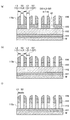
- FIG. 4A is a diagram for explaining the mask pattern forming method and the semiconductor device manufacturing method according to the first embodiment, following FIG. 4A, schematically showing the state of the wafer in each step.
- FIG. 4A is a diagram for explaining the mask pattern forming method and the semiconductor device manufacturing method according to the first embodiment, following FIG. 4A, schematically showing the state of the wafer in each step.
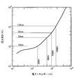
- FIG. 4B is a diagram for explaining the mask pattern forming method and the semiconductor device manufacturing method according to the first embodiment, following FIG. 4B, schematically showing the state of the wafer in each step. It is a schematic diagram for demonstrating the principle of the modification process performed by irradiating an electron to a line part in 1st Embodiment. It is a figure which shows the theoretical relationship between the electron energy when an electron is irradiated to a resist, and an electron penetration depth with a graph. In the conventional mask pattern formation method and semiconductor device manufacturing method, it is sectional drawing which shows typically the wafer after an etch-back process is performed.
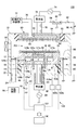
- a plasma processing apparatus 100 is configured as a capacitively coupled plasma etching apparatus, and includes a cylindrical chamber (processing vessel) 10 made of metal such as aluminum or stainless steel.
- the chamber 10 is grounded.
- a disk-shaped susceptor 12 on which a semiconductor wafer W (hereinafter referred to as "wafer W") is placed is horizontally disposed as a lower electrode.
- the susceptor 12 is made of, for example, aluminum, and is supported by an insulating cylindrical support portion 14 that extends vertically upward from the bottom of the chamber 10.
- An annular exhaust path 18 is formed between the conductive cylindrical support portion (inner wall portion) 16 extending vertically upward from the bottom of the chamber 10 and the side wall of the chamber 10 along the outer periphery of the cylindrical support portion 14. Yes.
- a ring-shaped exhaust ring (baffle plate) 20 is attached to the inlet of the exhaust path 18, and an exhaust port 22 is provided at the bottom of the exhaust path 18.
- An exhaust device 26 is connected to the exhaust port 22 via an exhaust pipe 24.
- the exhaust device 26 has a vacuum pump such as a turbo molecular pump, and can exhaust the processing space in the chamber 10 to a desired degree of vacuum.
- a gate valve 28 for opening and closing the loading / unloading port of the wafer W is attached to the side wall of the chamber 10.
- a high frequency power supply 30 is electrically connected to the susceptor 12 via a matching unit 32 and a lower power feed rod 36.
- the high frequency power supply 30 outputs high frequency power.
- This high-frequency power has a frequency (usually 13.56 MHz or less) that contributes to ion attraction to attract ions toward the wafer W on the susceptor 12.
- the matching unit 32 can match the impedance between the high-frequency power source 30 and the load (mainly electrodes, plasma, and chamber) and can automatically correct the matching impedance.
- the wafer W to be processed is placed on the susceptor 12.
- the susceptor 12 has a diameter larger than the diameter of the wafer W.
- a focus ring (correction ring) 38 surrounding the wafer W placed on the susceptor 12 is provided on the susceptor 12.
- An electrostatic chuck 40 for attracting wafers is provided on the upper surface of the susceptor 12.
- the electrostatic chuck 40 has a sheet-like or mesh-like conductor sandwiched between a film-like or plate-like dielectric.
- a DC power source 42 disposed outside the chamber 10 is electrically connected to the conductor via a switch 44 and a power supply line 46.
- the wafer W can be attracted and held on the electrostatic chuck 40 by a Coulomb force by a DC voltage applied from the DC power source 42.
- the susceptor 12 is provided with a temperature distribution adjusting unit 120.
- the temperature distribution adjusting unit 120 includes heaters 121a and 121b, heater power supplies 122a and 122b, thermometers 123a and 123b, and refrigerant flow paths 124a and 124b.
- a central heater 121a is provided in the central region, and an outer peripheral heater 121b is provided outside the central heater 121a.
- a center heater power source 122a is connected to the center heater 121a, and an outer side heater power source 122b is connected to the outer side heater 121b.
- the center side heater power source 122a and the outer side heater power source 122b respectively adjust the power supplied to the center side heater 121a and the outer side heater 121b to the susceptor 12 in a desired temperature distribution along the radial direction. Can be generated. Thereby, a desired temperature distribution along the radial direction can be generated on the wafer W.
- a center side thermometer 123a and an outer side thermometer 123b are provided inside the susceptor 12.
- the center-side thermometer 123a and the outer periphery-side thermometer 123b can measure the temperatures of the center region and the outer periphery region of the susceptor 12, and thereby derive the temperatures of the center region and the outer periphery region of the wafer W.
- a signal indicating the temperature measured by the center side thermometer 123a and the outer side thermometer 123b is sent to the temperature control unit 127.
- the temperature control unit 127 adjusts the outputs of the central heater power supply 122a and the outer peripheral heater power supply 122b so that the temperature of the wafer W derived from the measured temperature becomes the target temperature.
- the temperature control unit 127 is connected to a control unit 130 described later.
- a center side refrigerant flow path 124a is provided in the central region, and an outer peripheral side refrigerant flow path 124b is provided outside the center side refrigerant flow path 124a.
- refrigerants having different temperatures are circulated and supplied from chiller units (not shown).
- the refrigerant is introduced from the center side introduction pipe 125a into the center side refrigerant flow path 124a, circulated through the center side refrigerant flow path 124a, and then discharged from the center side refrigerant flow path 124a through the center side discharge pipe 126a. Is done.
- the refrigerant is introduced from the outer peripheral side introduction pipe 125b into the outer peripheral side refrigerant flow path 124b, circulated in the outer peripheral side refrigerant flow path 124b, and then discharged from the outer peripheral side refrigerant flow path 124b through the outer peripheral side discharge pipe 126b.
- the refrigerant for example, cooling water, a fluorocarbon liquid, or the like can be used.
- the temperature of the susceptor 12 is adjusted by heating by the center heater 121a and the outer heater 121b and cooling from the refrigerant. Accordingly, the wafer W is adjusted to have a predetermined temperature by transferring heat with the susceptor 12, including heating due to radiation from the plasma or irradiation of ions contained in the plasma. Moreover, in this Embodiment, the susceptor 12 has the center heater 121a and the center side refrigerant
- a heat transfer gas such as He gas from a heat transfer gas supply unit (not shown) is used as a gas passage inside the gas supply pipe 54 and the susceptor 12. It is supplied between the electrostatic chuck 40 and the wafer W via 56.
- an upper electrode 60 that is parallel to the susceptor 12 and also serves as a shower head.
- the upper electrode (shower head) 60 includes an electrode plate 62 facing the susceptor 12 and an electrode support 64 that detachably supports the electrode plate 62 from the back (upper) thereof.
- a gas diffusion chamber 66 is provided inside the electrode support 64.
- the electrode support 64 and the electrode plate 62 are formed with a plurality of gas discharge holes 68 that allow the gas diffusion chamber 66 and the internal space of the chamber 10 to communicate with each other.
- a space between the electrode plate 62 and the susceptor 12 becomes a plasma generation space or a processing space PS.
- the gas diffusion chamber 66 is connected to the processing gas supply unit 72 via a gas supply pipe 70.
- the electrode plate 62 of the upper electrode 60 is exposed to plasma during processing, it is preferably made of a material that does not adversely affect the process even if sputtered by ion bombardment from the plasma. Moreover, in this Embodiment, since the electrode plate 62 (especially the surface) functions as a DC application member, it is preferable that it has favorable electroconductivity with respect to a direct current. Examples of such materials include Si-containing conductive materials such as Si and SiC, and C (carbon). Moreover, the electrode support body 64 may be comprised, for example with the aluminum by which the alumite process was carried out.
- the upper electrode 60 is attached to the chamber 10 via a ring-shaped insulator 65 between the upper electrode 60 and the chamber 10. The upper electrode 60 is electrically floated from the chamber 10 by the insulator 65.
- a high frequency power source 74 is electrically connected to the upper electrode 60 via a matching unit 76 and an upper power feed rod 78.
- the high frequency power supply 74 outputs high frequency power having a frequency (usually 40 MHz or more) that contributes to plasma generation.
- the matching unit 76 can match the impedance between the high-frequency power source 74 and the load (mainly electrodes, plasma, and chamber), and can automatically adjust the matching impedance.
- variable DC power supply 80 installed outside the chamber 10 is electrically connected to the upper electrode 60 via a switch 82 and a DC power supply line 84.
- the variable DC power supply 80 can output a DC voltage VDC of ⁇ 2000 to +1000 V, for example.
- the filter circuit 86 provided in the middle of the DC power supply line 84 allows the DC voltage VDC from the variable DC power supply 80 to pass through the filter circuit 86 and be applied to the upper electrode 60.
- the filter circuit 86 can guide the high frequency to the ground line. For this reason, the high frequency from the susceptor 12 hardly flows to the variable DC power supply 80 via the processing space PS, the upper electrode 60, and the DC power supply line 84.
- a ring-shaped DC ground part (DC ground electrode) 88 made of a conductive material such as Si or SiC is attached to the upper surface of the baffle plate 20 in the chamber 10.
- the DC ground part 88 is always grounded via the ground line 90.
- the DC ground part 88 is not limited to the upper surface of the baffle plate 20 and may be provided at a position facing the processing space PS.
- the DC ground part 88 may be provided near the top of the cylindrical support part 16 or on the outer side in the radial direction of the upper electrode 60.
- the control unit 130 includes a processor (CPU) 152, a memory (RAM) 154, a program storage device (HDD) 156, a disk drive (DRV such as a flexible disk or an optical disk) connected via a bus 150. 158, an input device (KEY) 160 such as a keyboard and a mouse, a display device (DIS) 162, a network interface (COM) 164, and a peripheral interface (I / F) 166.
- CPU central processing unit
- RAM random access memory
- HDD program storage device
- D disk drive
- 158 an input device 160 such as a keyboard and a mouse
- DIS display device
- COM network interface
- I / F peripheral interface
- the processor (CPU) 152 reads a code of a required program from a storage medium 168 such as a flexible disk or an optical disk loaded in the disk drive (DRV) 158 and stores it in the HDD 156. Alternatively, a required program can be downloaded from the network via the network interface 164.
- the processor (CPU) 152 loads a program code necessary for the process to be executed from the program storage device (HDD) 156 onto the working memory (RAM) 154, executes each step, and performs a desired arithmetic processing. .
- the processor (CPU) 152 is connected to each part in the apparatus via the peripheral interface (I / F) 166, in particular, the exhaust device 26, the high frequency power supplies 30, 74, the processing gas supply unit 72, the variable DC power supply 80, and the switch 82.
- the temperature distribution adjusting unit 120 and the like are controlled.
- a processing gas including an etchant gas is introduced into the chamber 10 from the processing gas supply unit 72 at a predetermined flow rate, and the exhaust apparatus 26 Adjust the pressure to the set value. Further, a first high frequency (40 MHz or higher) for plasma generation is applied from the high frequency power source 74 to the upper electrode 60 via the matching unit 76 and the upper power feed rod 78, and at the same time, a second high frequency (13 .56 MHz) is applied to the susceptor 12 through the matching unit 32 and the lower power feed rod 36. Further, the switch 44 is turned on, and the wafer W is attracted to the electrostatic chuck 40 by the electrostatic adsorption force.
- a first high frequency 40 MHz or higher
- a second high frequency 13 .56 MHz
- the heat transfer gas (He gas) is confined in the contact interface between the wafer W and the electrostatic chuck 40.
- the processing gas discharged from the gas discharge hole 68 of the upper electrode 60 is turned into plasma in the processing space PS by the high frequency applied between the electrodes 12 and 60, and the radicals and ions generated in the plasma cause the target gas on the wafer W to become plasma.
- the processed film is etched into a desired pattern.
- a first high frequency wave having a relatively high frequency suitable for plasma generation of 40 MHz or higher (more preferably 60 MHz or higher) is applied from the high frequency power source 74 to the upper electrode 60.
- the plasma can be kept in a preferable dissociated state and can be densified, so that high-density plasma can be formed even under lower pressure conditions.
- a second high frequency wave having a relatively low frequency suitable for ion attraction of 13.56 MHz or less is applied to the susceptor 12.
- anisotropic etching with high selectivity to the film to be processed of the wafer W can be realized.
- the first high frequency for plasma generation is always used in any plasma process, but the second high frequency for ion attraction may not be used depending on the process.
- a DC voltage is applied to the upper electrode 60 from the variable DC power supply 80 (usually within a range of ⁇ 900 V to 0 V).
- plasma ignition stability, resist selectivity, etching rate, etching uniformity, etc. can also be improved.
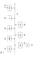
- the stacking step S11 is performed.
- an insulating film 111, an etching target film 112, a mask film 113, an antireflection film 114, and a resist film 115 are stacked on a wafer W made of, for example, a silicon substrate.
- the to-be-etched film 112 is a film to be finally etched in the semiconductor device manufacturing method including the mask pattern forming method according to the present embodiment.
- the insulating film 111 is, for example, a silicon oxide (SiO 2 ) film made of, for example, TEOS (tetraethoxysilane) that functions as a gate insulating film
- the film to be etched 112 is a polysilicon film that functions as a gate electrode after etching, for example. It can be.
- the thickness of the etching target film 112 can be set to 90 nm, for example.
- the mask film 113 functions as a hard mask when etching the etching target film 112 which is a lower layer film.
- a pattern of the third line portion 116a made of the silicon oxide film 116 formed in the silicon oxide film forming step S15 (described later) is transferred to the mask film 113.
- the mask film 113 preferably has a high selection ratio with respect to the etching target film 112 when the etching target film 112 is etched. That is, it is preferable that the ratio of the etching rate of the film to be etched 112 to the etching rate of the mask film 113 is large.
- an inorganic film such as a SiN film or a SiON film can be used.
- the thickness of the mask film 113 can be set to 26 nm, for example.
- the antireflection film 114 functions as an antireflection film (BARC) when exposing the resist film 115 formed thereon.
- BARC antireflection film
- an anti-reflection film 114 may be, for example, film or the like made of C x H y O z called organic BARC. Further, the thickness of the antireflection film 114 can be set to, for example, 30 nm.
- the resist film 115 is formed on the wafer W via the antireflection film 114.
- the resist film 115 is exposed and developed to provide a first line portion 115a that becomes a core material in the subsequent SWP.
- an ArF resist can be used as the resist film 115.
- the thickness of the resist film 115 can be set to 100 nm, for example.
- the photolithography step S12 is performed.
- the photolithography step S12 as shown in FIG. 4A (b), the first line portion 115a made of the resist film 115 is formed by using a photolithography technique.
- the resist film 115 formed on the antireflection film 114 is exposed and developed through a photomask (not shown) having a predetermined pattern, whereby the first film made of the resist film 115 is formed.
- a pattern including the line portion 115a is formed.
- the first line portion 115a functions as a mask when the antireflection film 114 is etched.
- the line width L1 and the space width S1 are not particularly limited, but both can be set to 60 nm, for example.
- a line part is a structure extended along a 1st direction on a plane, and it is a predetermined distance along the 2nd direction orthogonal to a 1st direction from the adjacent same structure.
- the line width is a length along the second direction of the line portion.
- the space width is the length along the second direction of the gap between two adjacent line portions.
- the interval at which the line portions are arranged is a distance between the center of one line portion and the center of the adjacent line portion.
- mask pattern forming steps S13 to S18 are performed.
- the wafer W is irradiated with plasma, and the first line portion 115a formed of the resist film 115 formed on the wafer W via the antireflection film 114 is used as a mask.
- 114 is etched.
- a pattern including the second line portion 114a made of the resist film 115 and the antireflection film 114 is formed.
- the antireflection film 114 is etched and the first line portion 115a is trimmed to obtain a line width L2 smaller than the line width L1 of the first line portion 115a.
- the second line portion 114a may be formed (FIG. 4A (c)).
- trimming of the first line portion 115a is also performed will be specifically described.
- a predetermined processing gas is introduced into the chamber 10 from the processing gas supply unit 72 of the plasma processing apparatus 100 at an appropriate flow rate, and the pressure in the chamber 10 is adjusted to a set value by the exhaust device 26.
- a first high frequency (40 MHz or higher) for plasma generation is applied from the high frequency power source 74 to the upper electrode 60 via the matching unit 76 and the upper power feed rod 78.
- the switch 44 is turned on, and the wafer W is attracted to the electrostatic chuck 40 by the electrostatic adsorption force.
- the heat transfer gas He gas
- the processing gas discharged from the gas discharge hole 68 of the upper electrode 60 is turned into plasma in the processing space PS by the high frequency applied between the electrodes 12 and 60.
- a CF gas such as CF 4 , C 4 F 8 , CHF 3 , CH 3 F, and CH 2 F 2 and a mixed gas such as Ar gas, or this A gas in which oxygen is added to the mixed gas as necessary can be used.
- the antireflection film 114 is etched using the first line portion 115a made of the resist film 115 as a mask, and the first line portion 115a itself is also trimmed. As a result, the resist film 115 and the antireflection film 114 are included, and the second line width L2 (FIG. 4A (c)) smaller than the line width L1 (FIG. 4A (b)) of the first line portion 115a.
- a line portion 114a is formed. That is, the magnitude relationship between the line width L1 and space width S1 of the first line portion 115a and the line width L2 and space width S2 of the second line portion 114a is L2 ⁇ L1, S2> S1.
- the values of L2 and S2 are not particularly limited. For example, L2 can be 30 nm and S2 can be 90 nm.
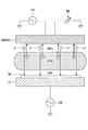
- the sheath voltage V U is approximately equal to the DC voltage.
- ions in the plasma PR (+) are accelerated by the electric field of the upper ion sheath SH U, it leads to a high kinetic energy.
- the ions collide with the upper electrode 60 (electrode plate 62) with large impact energy a large number of secondary electrons e ⁇ are emitted from the electrode plate 62.
- the secondary electrons e ⁇ emitted from the electrode plate 62 are accelerated in the direction opposite to the ions by the electric field of the upper ion sheath SH U , pass through the plasma PR, further cross the lower ion sheath SH L , and on the susceptor 12.
- the wafer W is driven with a large amount of energy. That is, the first line portion 115a made of the resist film 115 on the surface of the wafer W is irradiated with electrons.
- the resist polymer constituting the first line portion 115a absorbs the energy of the electrons, causing a composition change, a structure change, a crosslinking reaction, and the like. Thereby, the first line portion 115a is modified.
- the secondary electrons e ⁇ pass through the plasma PR at an equal speed, but the lower the sheath voltage V L (or the self-bias voltage) of the lower ion sheath SH L is better, and normally it is preferably 100 V or less. Therefore, the power of the second high frequency (13.56 MHz) applied to the susceptor 12 may be selected to be 50 W or less, more preferably 0 W.
- the electron energy and the electron penetration depth when electrons are injected into the resist are in a substantially proportional relationship as shown in FIG. According to this theory, the penetration depth when the electron energy is 600 eV is about 30 nm, the penetration depth when the electron energy is 1000 eV is about 50 nm, and the penetration depth when the electron energy is 1500 eV. 120 nm.
- the absolute value of the negative DC voltage V DC applied to the upper electrode 60 is preferably equal to or less than a predetermined absolute value V AB .
- the predetermined absolute value V AB can be set to 600 V, for example.
- the absolute value of the negative direct current voltage VDC can be set to 600 V, for example.
- the temperature distribution in the plane of the wafer W supported by the susceptor 12 may be adjusted.
- the distribution of the line width L2 of the second line portion 114a in the plane of the wafer W can be controlled.
- an irradiation step S14 is performed.
- the second line portion 114a made of the resist film 115 and the antireflection film 114 is irradiated with electrons.
- a predetermined processing gas is introduced into the chamber 10 from the processing gas supply unit 72 at an appropriate flow rate, and the pressure in the chamber 10 is set to a set value by the exhaust device 26. Adjust to. Then, a first high frequency (40 MHz or higher) for plasma generation is applied from the high frequency power source 74 to the upper electrode 60 via the matching unit 76 and the upper power feed rod 78. The processing gas discharged from the gas discharge hole 68 of the upper electrode 60 is turned into plasma in the processing space PS by the high frequency applied between the electrodes 12 and 60.
- the irradiation step S14 is performed not for etching but for modifying the second line portion 114a formed in the first pattern formation step S13. Therefore, as a processing gas, a processing gas having a large etching ability, for example, a processing gas having a small etching ability instead of a CF gas such as CF 4 , C 4 F 8 , CHF 3 , CH 3 F, CH 2 F 2 ,
- a processing gas having a small etching ability instead of a CF gas such as CF 4 , C 4 F 8 , CHF 3 , CH 3 F, CH 2 F 2 .
- hydrogen (H 2 ) gas and mixed gas such as Ar gas are used.
- the line width L2 of the second line portion 114a made of the resist film 115 and the antireflection film 114 hardly changes in the irradiation step S14.
- the DC voltage VDC is applied to the upper electrode 60 with a negative high voltage from the variable DC power source 80, as in the first pattern formation step S13.
- a DC voltage V DC to the upper electrode 60 increases the ion bombardment energy with which ions in the plasma PR (+) strikes the upper electrode 60 are accelerated by the electric field of the upper ion sheath SH U (electrode plate 62), Secondary electrons e ⁇ emitted from the electrode plate 62 by the discharge increase. The secondary electrons e ⁇ emitted from the electrode plate 62 are injected with a predetermined high energy into the surface of the wafer W on the susceptor 12.
- the absolute value of the negative DC voltage VDC applied to the upper electrode 60 is the predetermined absolute value described above. It may be larger than the V AB. Specifically, as described above, when the predetermined absolute value V AB is set to 600 V, for example, the absolute value of the negative direct current voltage V DC can be set to 900 V, for example.
- a silicon oxide film forming step S15 is performed.
- the silicon oxide film 116 is formed so as to cover the second line portion 114a isotropically.
- the silicon oxide film 116 is not limited to SiO 2, is formed of a material having other composition comprising SiO x and SiO 2 film composition ratio of oxygen and silicon are different, or silicon and oxygen as main components Also good. Further, the silicon oxide film 116 may be formed of silicon oxynitride (SiON).
- the silicon oxide film 116 is formed in a state where the resist film 115 and the antireflection film 114 remain as the second line portion 114a.
- a low temperature eg, about 300 ° C. or lower.
- Any method can be used for forming the silicon oxide film 116 as long as it can be formed at a low temperature.
- it can be performed by low-temperature molecular layer deposition (hereinafter referred to as MLD), that is, low-temperature MLD.
- MLD low-temperature molecular layer deposition
- a silicon oxide film 116 is formed on the entire surface of the wafer W, and the side surfaces of the second line portions 114a are also covered on the side surfaces of the second line portions 114a.
- a silicon oxide film 116 is formed.
- the thickness of the silicon oxide film 116 at this time is D
- the width of the silicon oxide film 116 covering the side surface of the second line portion 114a is also D.
- the thickness D of the silicon oxide film 116 can be set to 30 nm, for example.
- a silicon oxide film forming process by low temperature MLD will be described.
- a source gas containing silicon is supplied into a processing container of a film forming apparatus, a silicon source is adsorbed on the wafer W, a gas containing oxygen is supplied into the processing container, and the silicon source is oxidized.
- the process of making it repeat alternately.
- an aminosilane gas having two amino groups in one molecule for example, a bister-sharp
- BTBAS Butylaminosilane
- an oxidation process in the process of supplying oxygen-containing gas into the processing vessel and oxidizing the BTBAS adsorbed on the wafer W (hereinafter referred to as an oxidation process), for example, plasma generation with a high-frequency power source is used as the oxygen-containing gas.
- O 2 gas converted into plasma by the mechanism is supplied into the processing container through a gas supply nozzle for a predetermined time.
- the BTBAS adsorbed on the wafer W is oxidized, and a silicon oxide film 116 is formed.
- a process (hereinafter referred to as a purge process) of supplying a purge gas into the processing container while evacuating the processing container is performed for a predetermined time. be able to. Therefore, the adsorption process, the purge process, the oxidation process, and the purge process are repeated in this order.
- the purge gas for example, an inert gas such as nitrogen gas can be used.
- the purge process is not limited as long as the gas remaining in the processing container can be removed. For this reason, in the purge process, the inside of the processing container may be simply evacuated without supplying the purge gas (without supplying the source gas).
- a source gas containing organic silicon other than BTBAS may be used for forming the silicon oxide film 116 by low temperature MLD.
- An example of a source gas containing organic silicon is an aminosilane-based precursor.
- An example of the aminosilane precursor is a monovalent or divalent aminosilane precursor. Specific examples of monovalent or divalent aminosilane precursors include BTBAS (Bisthal butylaminosilane), BDMAS (Bisdimethylaminosilane), BDEAS (Bisdiethylaminosilane), DPAS (Dipropylaminosilane), BAS (Butylaminosilane) , And DIPAS (diisopropylaminosilane).
- a trivalent aminosilane precursor can be used as the aminosilane precursor.
- An example of a trivalent aminosilane-based precursor is TDMAS (tridimethylaminosilane).
- an ethoxysilane precursor can be used in addition to an aminosilane precursor.
- An example of the ethoxysilane precursor is, for example, TEOS (tetraethoxysilane).
- gas containing oxygen in addition to O 2 gas, NO gas, N 2 O gas, H 2 O gas, and O 3 gas can be used, and these are converted into plasma by a high frequency electric field and used as an oxidizing agent. Can do.
- plasma of such a gas containing oxygen the silicon oxide film can be formed at 300 ° C. or lower.
- the silicon oxide film can be formed at 100 ° C. or lower or at room temperature.
- an etch back step S16 is performed.
- the silicon oxide film 116 is removed from the upper portion of the second line portion 114a and, as shown in FIG. 4B (f), left as the side wall portion 116a of the second line portion 114a. Then, the silicon oxide film 116 is etched back.
- a predetermined processing gas is introduced into the chamber 10 at an appropriate flow rate from the processing gas supply unit 72 in the plasma processing apparatus 100 again, and the pressure in the chamber 10 is adjusted to a set value by the exhaust device 26. To do. Then, a first high frequency (40 MHz or higher) for plasma generation is applied from the high frequency power source 74 to the upper electrode 60 via the matching unit 76 and the upper power feed rod 78. Then, the processing gas discharged from the shower head 60 is dissociated and ionized by high-frequency discharge between the electrodes 12 and 60 to generate plasma.
- a first high frequency 40 MHz or higher
- a CF gas such as CF 4 , C 4 F 8 , CHF 3 , CH 3 F, or CH 2 F 2 and a mixed gas such as Ar gas or a mixed gas as the processing gas.
- a gas to which oxygen is added can be used as necessary.
- the silicon oxide film 116 is anisotropically etched mainly along a direction perpendicular to the surface of the wafer W. As a result, the silicon oxide film 116 is removed from the upper part of the second line portion 114a and remains only as a side wall portion 116a that covers the side surface of the second line portion 114a. At this time, the silicon oxide film 116 formed in the space portion between the second line portion 114a and the adjacent second line portion 114a is also removed.
- the second line portion 114a whose side surface is covered with the side wall portion 116a is referred to as a side surface covering line portion 114b.
- an etching step S17 for etching the mask film 113 is performed.
- the mask film 113 is etched using the side surface covering line portion 114b including the side wall portion 116a and the second line portion 114a as a mask.
- a predetermined processing gas is introduced into the chamber 10 from the processing gas supply unit 72 at an appropriate flow rate, and a first high frequency (40 MHz or higher) for plasma generation is applied to the upper electrode 60 and at the same time for ion attraction.
- the second high frequency 13.56 MHz is applied to the susceptor 12.
- the supplied processing gas is turned into plasma by high-frequency discharge between the electrodes 12 and 60, and the mask film 113 is etched by radicals and ions generated by the plasma.
- a processing gas for example, a CF-based gas such as CF 4 , C 4 F 8 , CHF 3 , CH 3 F, or CH 2 F 2 and a mixed gas such as Ar gas, or this mixed gas is necessary.
- a gas to which oxygen is added can be used.
- the mask film 113 is etched in the region R1 that is a space portion between the side surface covering line portion 114b and the adjacent side surface covering line portion 114b.
- a second pattern forming step S18 is performed.
- the second line portion 114a made of the resist film 115 and the antireflection film 114 is ashed.
- a mask pattern including the third line portion 116a remaining as the side wall portion 116a made of the silicon oxide film 116 is formed.
- a cross section of the wafer W when the second pattern formation step S18 is completed is shown in FIG. 4C (g).
- a predetermined processing gas is introduced into the chamber 10 from the processing gas supply unit 72 at an appropriate flow rate, and simultaneously with the application of the first high frequency (40 MHz or higher) for plasma generation to the upper electrode 60. Then, a second high frequency (13.56 MHz) for ion attraction is applied to the susceptor 12.
- the supplied processing gas is turned into plasma by high-frequency discharge between the electrodes 12 and 60, and the second line portion 114a composed of the resist film 115 and the antireflection film 114 is formed by radicals and ions generated by the plasma. Ashed.
- a mixed gas such as hydrogen (H 2 ) gas or nitrogen (N 2 ) gas can be used as the processing gas.
- the second line portion 114a made of the resist film 115 and the antireflection film 114 is ashed, and the third line portion made of the silicon oxide film 116 remains as the side wall portion 116a.
- a pattern including 116a is formed.
- the third line portion 116a functions as a mask when the mask film 113 is etched.
- the line width of the third line portion 116a is L3 and the space widths are S3 and S3 ′
- the line width L2 of the second line portion 114a is 30 nm and the thickness D of the side wall portion 116a is 30 nm
- L3 can be set to 30 nm
- S3 and S3 ′ can be set to 30 nm.
- a mask film etching step S19 is performed.
- the mask film 113 is etched by plasma irradiated on the wafer W using the third line portion 116a as a mask.
- a fourth line portion 113a made of the mask film 113 is formed.
- a predetermined processing gas is introduced into the chamber 10 from the processing gas supply unit 72 at an appropriate flow rate, and at the same time as a first high frequency (40 MHz or more) for plasma generation is applied to the upper electrode 60, A second high frequency (13.56 MHz) for drawing is applied to the susceptor 12.
- the supplied processing gas is turned into plasma by high-frequency discharge between the electrodes 12 and 60, and the mask film 113 is etched by radicals and ions generated by the plasma.
- a processing gas for example, a CF-based gas such as CF 4 , C 4 F 8 , CHF 3 , CH 3 F, or CH 2 F 2 and a mixed gas such as Ar gas, or this mixed gas
- a gas to which oxygen is added can be used as necessary.
- the mask film 113 is etched using the third line portion 116a made of the silicon oxide film 116 as a mask.
- the fourth line portion 113a made of the mask film 113 and having substantially the same line width as the third line portion 116a is formed.
- an etching target film etching step S20 is performed.
- the etching target film 112 is etched by the plasma irradiated to the wafer W using the fourth line portion 113a made of the mask film 113 as a mask, as shown in FIG. 4C (i). Then, a fifth line portion 112a made of the etching target film 112 is formed.
- a predetermined processing gas is introduced into the chamber 10 from the processing gas supply unit 72 at an appropriate flow rate, and simultaneously with applying a first high frequency (40 MHz or more) for plasma generation to the upper electrode 60, A second high frequency (13.56 MHz) for ion attraction is applied to the susceptor 12.
- the supplied processing gas is turned into plasma by high-frequency discharge between the electrodes 12 and 60, and the film to be etched 112 is etched by radicals and ions generated by the plasma.
- a processing gas for example, a CF-based gas such as CF 4 , C 4 F 8 , CHF 3 , CH 3 F, or CH 2 F 2 and a mixed gas such as Ar gas, or a mixture thereof
- a gas in which oxygen is added to the gas as necessary can be used.
- the etching target film 112 is etched using the fourth line portion 113a made of the mask film 113 as a mask.
- the fifth line portion 112a which is made of the film to be etched 112 and has substantially the same line width as the third line portion 116a and the fourth line portion 113a, is formed.
- the temperature distribution in the plane of the wafer W supported by the susceptor 12 may be adjusted. By this adjustment, as will be described later, the distribution of the line width L3 of the fifth line portion 112a in the surface of the wafer W can be controlled.
- FIG. 7 is a cross-sectional view schematically showing the state of the wafer W after the etch back step S16 is performed in the conventional mask pattern forming method and semiconductor device manufacturing method.
- the resist film 115 such as an ArF resist has low plasma resistance or etching resistance
- the surface of the second line portion 114a made of the resist film 115 is roughened or the side surface of the second line portion 114a is formed during plasma etching. Tends to be uneven, and LER (Line Edge Roughness) and LWR (Line Width Roughness) deteriorate. Further, since the second line portion 114a has a very narrow width, the second line portion 114a also appears to meander when viewed from above due to the unevenness of the side surface of the second line portion 114a. And LWR may be further deteriorated.
- the second line portion 114a made of such a resist film 115 is used as the SWP core material
- the silicon oxide film 116 is formed in the silicon oxide film forming step S15
- the second line portion 114a is used. Will be exposed to plasma. When exposed to plasma, the surface of the second line portion 114a may become rough or deform. Further, when the silicon oxide film 116 is etched back in the etch back step S16, the silicon oxide film 116 above the second line portion 114a is removed, so that the second line portion 114a is exposed to plasma. Therefore, the surface of the second line portion 114a may be roughened or deformed.
- the side wall portion 116a is formed.
- the third line portions 116a are alternately arranged with different space widths, and there is a possibility that the third line portions 116a having a desired shape cannot be formed.
- the line width L2t on the upper end side of the second line portion 114a is larger than the line width L2b on the root side. May be smaller. This is because the upper end side of the second line portion 114a is easily exposed to plasma. In such a case, the side wall portion 116a cannot be formed perpendicularly to the surface of the wafer W, but alternately tilts in the opposite direction, so that the third line portion 116a having a desired shape can be formed. It may not be possible.
- the side surface of the second line portion 114a becomes uneven, and the side wall of the side wall portion 116a also becomes uneven.
- the above-described LER, LWR, or the like of the third line portion 116a made of the side wall portion 116a may deteriorate, and the third line portion 116a having a desired shape may not be formed.
- the deformed shape is transferred when the lower mask layer 113 and the etching target film 112 are sequentially etched using the side wall portion 116a as a mask. Therefore, when the etching target film 112 is etched to form the fifth line portion 112a, the fifth line portion 112a cannot be formed with high accuracy.
- the second line portion 114a is modified by irradiating the second line portion 114a made of the resist film 115 with electrons. .
- the second line portion which is a core material is formed.
- the deformation of 114a can be prevented.
- the shape formed by the etching can be accurately performed when the lower layer film is etched using the second line portion 114a as a mask.
- the pattern formed by etching can be prevented from falling.
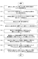
- FIG. 8 is a flowchart for explaining the procedure of each step in another example of the mask pattern forming method and the semiconductor device manufacturing method according to the present embodiment.
- a first pattern formation step S13 ′ is performed.
- a pattern including the second line 114a is formed by etching the antireflection film 114 without irradiating electrons.
- each process other than the first pattern formation process S13 ′) is the same as each process in FIG.
- Example 1 and Example 2 were carried out, and by comparison with Comparative Example 1, the shape of the second line part 114a whose side surface was covered with the side wall part 116a was evaluated.
- the evaluation result will be described with reference to Table 1.
- Example 1 As Example 1, steps S11 to S18 in FIG. 3 were performed. The conditions of each process of step S13, step S14, step S16 to step S18 in Example 1 are shown below.
- (A) First pattern formation step S13 Pressure inside the film forming apparatus: 800 mTorr High frequency power supply (40MHz / 13MHz): 200 / 0W Upper electrode potential: -600V Wafer temperature: center side / outer peripheral side 30/30 ° C.
- Process gas flow rate: CF 4 / O 2 / Ar 150/50/1000 sccm Processing time: 30 seconds
- Process gas flow rate: H 2 / Ar 450/450 sccm Processing time: 10 seconds
- Process gas flow rate: CF 4 / CHF 3 / O 2 125/125/20 sccm Processing time: 12 seconds
- Second pattern formation step S18 Pressure inside the film forming apparatus: 100 mTorr High frequency power supply (40MHz / 13MHz): 500 / 0W Upper electrode potential: 0V Wafer temperature: center side / outer peripheral side 30/30 ° C.
- Process gas flow rate: H 2 / N 2 300/900 sccm Processing time: 60 seconds (Example 2)
- each process of step S11 to step S18 in FIG. 8 was performed.
- the conditions of steps S14 and S16 to S18 in the second embodiment are the same as those in the first embodiment.
- step S13 'in Example 2 the conditions of step S13 'in Example 2 are shown below.
- (F) 1st pattern formation process S13 ') Pressure inside the film forming apparatus: 800 mTorr High frequency power supply (40MHz / 13MHz): 200 / 0W Upper electrode potential: 0V Wafer temperature: center side / outer peripheral side 30/30 ° C.
- Process gas flow rate: CF 4 / O 2 / Ar 150/20/1000 sccm Processing time: 55 seconds
- Step S14 in FIG. 8 was omitted, and Steps S11, S12, Step S13 ′, and Steps S15 to S18 were performed.
- the conditions of each step from Step S16 to Step S18 in Comparative Example 1 are the same as in Example 1.
- the condition of Step S13 ′ in Comparative Example 1 is the same as that in Example 2.
- Table 1 shows the line width L2 of the second line portion 114a whose side surface is covered with the side wall portion 116a after the process up to the etch-back step S16 in Example 1, Example 2, and Comparative Example 1.
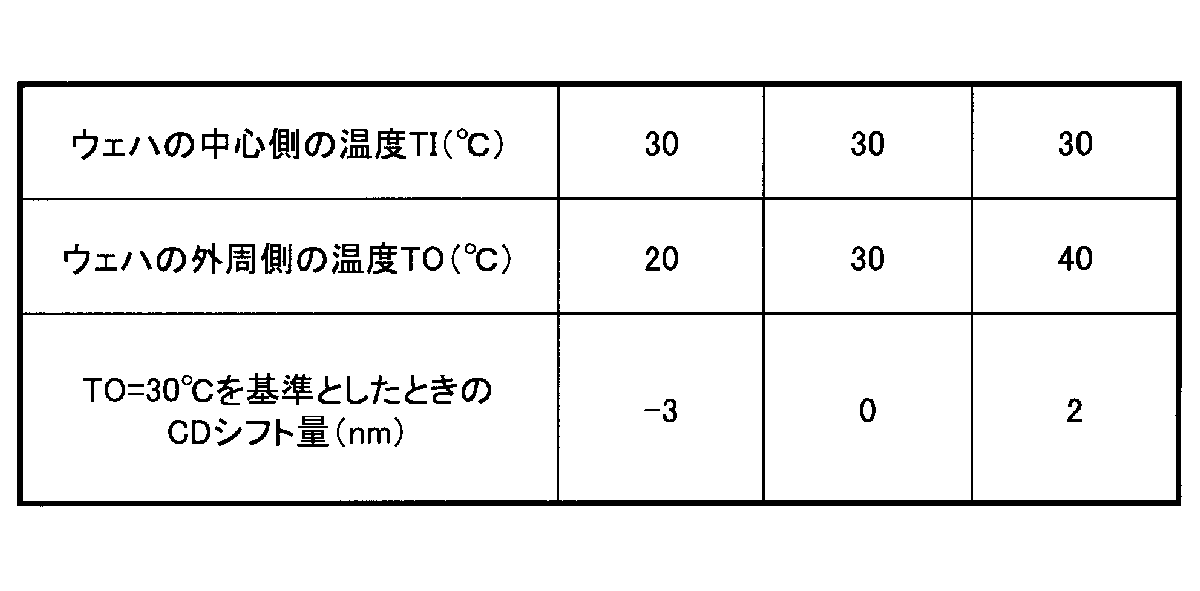
- the temperature distribution of the wafer W is adjusted by changing the temperature TO on the outer peripheral side while keeping the temperature TI on the center side of the wafer W constant (30 ° C.) under the condition (A) described above.
- the variation of the line width CD in the W plane was determined.
- Other conditions are the same as the above-mentioned condition (A).
- Table 2 shows the CD shift amount at the outermost periphery of the wafer W when the temperature TO on the outer peripheral side of the wafer W is 20 ° C., 30 ° C., and 40 ° C., based on the case where the temperature TO on the outer peripheral side is 30 ° C. .
- the size of the wafer W was 300 mm ⁇ .
- the CD shift amount refers to the line width L1 of the first line portion 115a before trimming (first pattern formation step S13) and the second line portion 114a after trimming (first pattern formation step S13). Means a difference from the line width L2.
- the CD shift amount at the outermost periphery of the wafer W is 30 ° C. on the outer peripheral side. It is 3 nm smaller than there are. Further, when the temperature TO on the outer peripheral side is 40 ° C., which is 10 ° C. higher than the temperature TI on the center side, the CD shift amount at the outermost periphery of the wafer W is larger than that when the temperature TO on the outer peripheral side is 30 ° C. 2 nm larger.
- the line width L2 of the second line width 114a after the trimming process (first pattern formation step S13) is adjusted to the center of the wafer W by independently adjusting the temperature TI on the center side and the temperature TO on the outer peripheral side. It is possible to control independently on the side and the outer peripheral side.
- the distribution of the line width L2 of the second line portion 114a in the plane of the wafer W is adjusted by adjusting the temperature distribution in the plane of the wafer W supported by the susceptor 12 in the first pattern formation step S13. Can be made uniform.
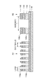
- FIG. 9 is a cross-sectional view schematically showing the state of the wafer W provided with the dense portion A1 and the sparse portion A2.
- a region where the third line portions 116a are arranged at a relatively small distance D21 (S3 + L3) (hereinafter referred to as a “dense portion”) is provided.
- a portion where the region A1 is provided is protected with a resist film or the like, and a third resist layer made of another resist film is provided on the portion where the region A2 is provided.
- a pattern including the line portion 116b is formed.
- the fifth line portions 112a and 112b are formed by performing the mask film etching step S19 and the etching target film etching step S20 using the mask pattern including the formed third line portions 116a and 116b.
- An area A1 in which the fifth line portions 112a are arranged at a relatively small distance D21 (S3 + L3) is provided on the left side of FIG. 9, and a relatively large area (larger than the distance D21) is provided on the right side of FIG. )
- a region A2 in which the fifth line portions 112b are arranged at the interval D22 is provided.
- the dense part A1 is provided by performing the processes from step S11 to step S18 in FIG. 3 under the conditions shown in (A) to (E) shown in the first embodiment, and the sparse part A2 is separately provided. Thereafter, Step S19 was performed under the same conditions as Step S17 shown in (D), and Step S20 was further executed under the conditions shown in (G) below.
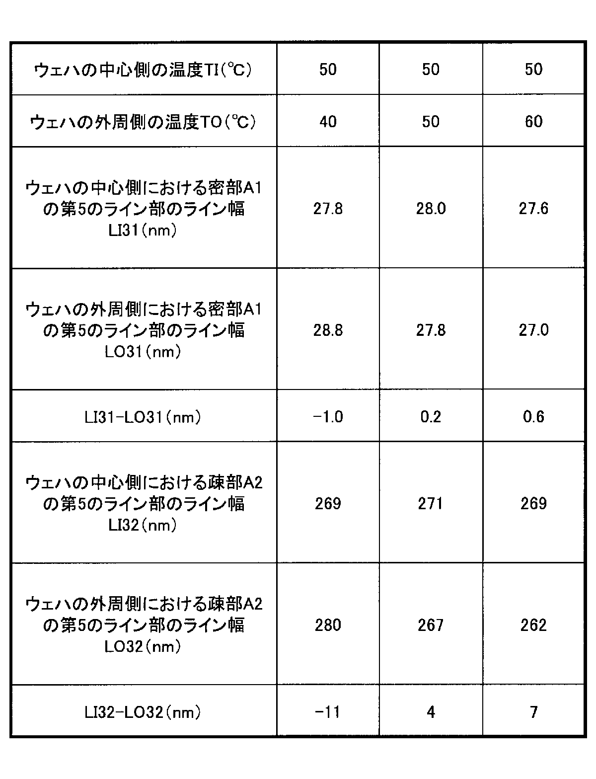
- Step S20 the temperature distribution in the plane of the wafer W was adjusted by changing the temperature TO on the outer peripheral side while keeping the temperature TI on the center side of the wafer W constant (50 ° C.). Then, the line widths of the fifth line portions 112a and 112b in the dense portion A1 and the sparse portion A2 were obtained.
- Table 3 shows the numbers of the dense part A1 and the sparse part A2 on the center side and the outer peripheral side of the wafer W when the temperature TO on the outer peripheral side of the wafer W is 40 ° C., 50 ° C., and 60 ° C., respectively.
- 5 shows the line widths of the five line portions 112a and 112b.
- the line widths of the fifth line portions 112a of the dense portion A1 on the center side and the outer peripheral side of the wafer W are set to LI31 and LO31, respectively.
- the line widths of the fifth line portions 112b of the sparse portion A2 on the center side and the outer peripheral side of the wafer W are set to LI32 and LO32, respectively.
- the difference LI32 ⁇ LO32 in the line width of the fifth line portion 112b of the sparse portion A2 between the center side and the outer peripheral side of the wafer W is ⁇ It can be freely changed from 11 nm to 7 nm. Therefore, since LI32-LO32 can be set to 0, the distribution of the line widths of the fifth line portions 112b of the sparse portion A2 on the center side and the outer peripheral side of the wafer W can be made uniform.
- the difference in the line width of the sparse part A2 between the center side and the outer periphery side of the wafer W is the wafer W having the line width of the dense part A1. Changes more than the difference between the center side and the outer periphery side. This is presumably because the fifth line portion 112b in the sparse portion A2 is more likely to react with the plasma than the fifth line portion 112a in the dense portion A1.
- the reaction rate at which the fifth line portions 112a and 112b react with the plasma, and the adhesion coefficient at which the reaction products generated by the reaction reattach to the fifth line portions 112a and 112b depend on the temperature. Therefore, when the temperature of the wafer W is changed, the line width of the fifth line portion 112b in the sparse portion A2 changes more than the line width of the fifth line portion 112a in the dense portion A1.
- the line width can be largely changed in the sparse part A2 than in the dense part A1.
- the line width LI31 at the center-side dense portion A1 and the line width LO31 at the outer periphery-side dense portion A1 are substantially equal, and the line width LI32 at the center-side sparse portion A2 and the outer periphery side
- the line width LO32 in the sparse part A2 can be made substantially equal.
- the second oxide which becomes the core material of the sidewall portion 116a before the silicon oxide film 116 which becomes the sidewall portion 116a is formed.
- the second line part 114a is modified by irradiating the line part 114a with electrons.
- the temperature distribution in the plane of the wafer W is adjusted in any of the first pattern forming step S13 and the etching target film etching step S20. Thereby, the distribution of the line widths of the second line portion 114a and the fifth line portion 112a on the center side and the outer peripheral side of the wafer W can be made uniform.
- the example in which the antireflection film 114 is etched and the first line portion 115a is trimmed in the first pattern formation step S13 has been described.
- the first line portion 115a is not trimmed in the first pattern formation step S13, that is, when the line width L2 of the second line portion 114a is substantially equal to the line width L1 of the first line portion 115a.
- the present embodiment is applicable. And the same effect as the trimming process is produced.
- This embodiment is different from the first embodiment in that the temperature distribution in the surface of the wafer W is not adjusted in any of the first pattern forming step S13 and the etching target film etching step S20.
- FIG. 10 is a schematic cross-sectional view showing a plasma processing apparatus 100a suitable for carrying out the mask pattern forming method according to the present embodiment.
- the same parts as those described with reference to FIG. 10 are identical to FIG. 10 in FIG. 10, the same parts as those described with reference to FIG. 10 in FIG. 10, the same parts as those described with reference to FIG. 10 in FIG. 10, the same parts as those described with reference to FIG. 10 in FIG. 10, the same parts as those described with reference to FIG.
- the plasma processing apparatus 100a has been described with reference to FIG. 1 in the first embodiment in that the susceptor 12 is not provided with a temperature distribution adjusting unit. Different from the plasma processing apparatus 100.
- the plasma processing apparatus 100 is the same as that described with reference to FIG. 1 except that the temperature distribution adjusting unit is not provided.
- the temperature distribution adjusting unit is not provided, and an annular coolant channel 48 extending in the circumferential direction, for example, is only provided inside the susceptor 12.
- a coolant having a predetermined temperature for example, cooling water, is circulated and supplied to the coolant channel 48 via pipes 50 and 52 from a chiller unit (not shown).
- the temperature of the wafer W on the electrostatic chuck 40 can be controlled by the temperature of the coolant.
- a heat transfer gas for example, He gas
- a heat transfer gas supply unit (not shown) is introduced into the gas supply pipe 54 and the susceptor 12. Is supplied between the electrostatic chuck 40 and the wafer W through the gas passage 56.
- the mask pattern forming method and the semiconductor device manufacturing method according to the present embodiment can be the same as the method according to the first embodiment described with reference to FIGS.
- the plasma processing apparatus 100a that does not have the temperature distribution adjustment unit is used, the surface of the wafer W is used in both the first pattern forming step S13 and the etching target film etching step S20. Do not adjust the temperature distribution inside.
- the second line portion 114a serving as a core material of the side wall portion 116a is formed before the silicon oxide film 116 to be the side wall portion 116a is formed.
- the second line portion 114a is modified by irradiating with electrons.
- This embodiment is also applicable to the case where the first line portion 115a is not trimmed in the first pattern forming step S13, and has the same effect as the case of trimming. Also in this embodiment, electrons may be irradiated after the photolithography step S12 and before the first pattern formation step S13.
Landscapes
- Physics & Mathematics (AREA)
- Engineering & Computer Science (AREA)
- Plasma & Fusion (AREA)
- Chemical & Material Sciences (AREA)
- Analytical Chemistry (AREA)
- Drying Of Semiconductors (AREA)
- Exposure And Positioning Against Photoresist Photosensitive Materials (AREA)
- Exposure Of Semiconductors, Excluding Electron Or Ion Beam Exposure (AREA)
Abstract
Description
(第1の実施の形態)
図1から図9を参照し、本発明の第1の実施の形態に係るマスクパターンの形成方法及び半導体装置の製造方法について説明する。
図1を参照すると、プラズマ処理装置100は、容量結合型のプラズマエッチング装置として構成されており、例えばアルミニウム又はステンレス鋼等の金属製の円筒型チャンバ(処理容器)10を有している。チャンバ10は接地されている。
低温MLDにおいては、シリコンを含む原料ガスを成膜装置の処理容器内に供給し、シリコン原料をウエハW上に吸着させる工程と、酸素を含むガスを処理容器内に供給し、シリコン原料を酸化させる工程とを交互に繰り返す。
実施例1として、図3におけるステップS11からステップS18の各工程を行った。実施例1におけるステップS13、ステップS14、ステップS16からステップS18の各工程の条件を以下に示す。
(A)第1のパターン形成工程S13
成膜装置内圧力 :800mTorr
高周波電源パワー(40MHz/13MHz):200/0W
上部電極の電位 :-600V
ウエハ温度 :中心側/外周側=30/30℃
処理ガスの流量 :CF4/O2/Ar=150/50/1000sccm
処理時間 :30秒
(B)照射工程S14
成膜装置内圧力 :100mTorr
高周波電源パワー(40MHz/13MHz):500/0W
上部電極の電位 :-900V
ウエハ温度 :中心側/外周側=30/30℃
処理ガスの流量 :H2/Ar=450/450sccm
処理時間 :10秒
(C)エッチバック工程S16
成膜装置内圧力 :30mTorr
高周波電源パワー(40MHz/13MHz):500/100W
上部電極の電位 :300V
ウエハ温度 :中心側/外周側=30/30℃
処理ガスの流量 :C4F6/Ar/O2=15/450/22.5sccm
処理時間 :25秒
(D)エッチング工程S17
成膜装置内圧力 :30mTorr
高周波電源パワー(40MHz/13MHz):400/0W
上部電極の電位 :0V
ウエハ温度 :中心側/外周側=30/30℃
処理ガスの流量 :CF4/CHF3/O2=125/125/20sccm
処理時間 :12秒
(E)第2のパターン形成工程S18
成膜装置内圧力 :100mTorr
高周波電源パワー(40MHz/13MHz):500/0W
上部電極の電位 :0V
ウエハ温度 :中心側/外周側=30/30℃
処理ガスの流量 :H2/N2=300/900sccm
処理時間 :60秒
(実施例2)
実施例2として、図8におけるステップS11からステップS18の各工程を行った。実施例2におけるステップS14、ステップS16からステップS18の各工程の条件は、実施例1と同様である。また、実施例2におけるステップS13´の条件を以下に示す。
(F)第1のパターン形成工程S13´)
成膜装置内圧力 :800mTorr
高周波電源パワー(40MHz/13MHz):200/0W
上部電極の電位 :0V
ウエハ温度 :中心側/外周側=30/30℃
処理ガスの流量 :CF4/O2/Ar=150/20/1000sccm
処理時間 :55秒
(比較例1)
比較例1として、図8におけるステップS14を省略し、ステップS11、ステップS12、ステップS13´、ステップS15からステップS18の各工程を行った。比較例1におけるステップS16からステップS18の各工程の条件は、実施例1と同様である。また、比較例1におけるステップS13´の条件は、実施例2と同様である。

表1に示すように、比較例1ではL2=25.6nmであるが、実施例2ではL2=28.3nmとなり、実施例2では比較例1に比べ、第2のライン部114aのライン幅L2が大きくなった。従って、照射工程S14において電子を照射することによって、酸化シリコン膜成膜工程S15及びエッチバック工程S16において第2のライン部114aが変形することを防止できる。
(G)被エッチング膜エッチング工程S20
成膜装置内圧力 :25mTorr
高周波電源パワー(40MHz/13MHz):1500/1500W
上部電極の電位 :300V
ウエハ温度 :中心側=50℃
処理ガスの流量 :C4F8/Ar/O2=50/700/37sccm
処理時間 :40秒
表3は、ウエハWの外周側の温度TOが40℃、50℃、60℃のときの、ウエハWの中心側及び外周側における、それぞれ密部A1、疎部A2の第5のライン部112a、112bのライン幅を示す。表3において、ウエハWの中心側及び外周側における密部A1の第5のライン部112aのライン幅を、それぞれLI31及びLO31とする。また、ウエハWの中心側及び外周側における疎部A2の第5のライン部112bのライン幅を、それぞれLI32及びLO32とする。
次に、図10を参照し、本発明の第2の実施の形態に係るマスクパターンの形成方法について説明する。
Claims (7)
- 反射防止膜上に形成されたフォトレジスト膜よりなる第1のライン部をマスクとして前記反射防止膜をエッチングすることによって、前記フォトレジスト膜と前記反射防止膜とよりなる第2のライン部を含むパターンを形成する第1のパターン形成工程と、
前記フォトレジスト膜に電子を照射する照射工程と、
前記第2のライン部を等方的に被覆するように酸化シリコン膜を成膜する酸化シリコン膜成膜工程と、
前記酸化シリコン膜を、前記第2のライン部の上部から除去するとともに、前記第2のライン部の側壁部として残存するように、前記酸化シリコン膜をエッチバックするエッチバック工程と、
前記第2のライン部をアッシングすることによって、前記酸化シリコン膜よりなり、前記側壁部として残存する第3のライン部を含むマスクパターンを形成する第2のパターン形成工程と
を有する、マスクパターンの形成方法。 - 前記照射工程において、前記第2のライン部に含まれている前記フォトレジスト膜に電子が照射される、請求項1に記載のマスクパターンの形成方法。
- 前記第1のパターン形成工程は、前記第1のライン部に電子を照射しながら、前記反射防止膜をエッチングするものである、請求項1に記載のマスクパターンの形成方法。
- 前記第1のパターン形成工程が、前記第1のライン部をトリミングする工程を更に含み、前記第1のライン部の線幅よりも小さな線幅を有し、前記フォトレジスト膜と前記反射防止膜とよりなる前記第2のライン部を含むパターンが形成される、請求項1に記載のマスクパターンの形成方法。
- 前記第1のパターン形成工程において、前記基板の面内における温度分布を調整することによって、前記基板の面内における前記第2のライン部の線幅の分布が制御される、請求項1に記載のマスクパターンの形成方法。
- 基板上に、被エッチング膜、マスク膜、前記反射防止膜、及び前記フォトレジスト膜を積層する積層工程と、
フォトリソグラフィ技術を用いて、前記フォトレジスト膜から前記第1のライン部を形成するフォトリソグラフィ工程と、
請求項1に記載のマスクパターンの形成方法により、前記マスクパターンを形成するマスクパターン形成工程と、
形成された前記マスクパターンを用いて前記マスク膜をエッチングすることによって、前記マスク膜よりなる第4のライン部を形成するマスク膜エッチング工程と、
形成された前記第4のライン部をマスクとして前記被エッチング膜をエッチングすることによって、前記被エッチング膜よりなる第5のライン部を形成する被エッチング膜エッチング工程と
を有する、半導体装置の製造方法。 - 前記被エッチング膜エッチング工程は、前記基板の面内における温度分布を調整することによって、前記基板の面内における前記第5のライン部の線幅の分布を制御するものである、請求項6に記載の半導体装置の製造方法。
Priority Applications (3)
| Application Number | Priority Date | Filing Date | Title |
|---|---|---|---|
| KR1020127028853A KR101427505B1 (ko) | 2010-04-02 | 2011-03-28 | 마스크 패턴의 형성 방법 및 반도체 장치의 제조 방법 |
| US13/638,662 US20130023120A1 (en) | 2010-04-02 | 2011-03-28 | Method of forming mask pattern and method of manufacturing semiconductor device |
| CN201180018012.1A CN102822943B (zh) | 2010-04-02 | 2011-03-28 | 掩模图案的形成方法以及半导体装置的制造方法 |
Applications Claiming Priority (2)
| Application Number | Priority Date | Filing Date | Title |
|---|---|---|---|
| JP2010-085956 | 2010-04-02 | ||
| JP2010085956A JP4733214B1 (ja) | 2010-04-02 | 2010-04-02 | マスクパターンの形成方法及び半導体装置の製造方法 |
Publications (1)
| Publication Number | Publication Date |
|---|---|
| WO2011125605A1 true WO2011125605A1 (ja) | 2011-10-13 |
Family
ID=44461724
Family Applications (1)
| Application Number | Title | Priority Date | Filing Date |
|---|---|---|---|
| PCT/JP2011/057618 Ceased WO2011125605A1 (ja) | 2010-04-02 | 2011-03-28 | マスクパターンの形成方法及び半導体装置の製造方法 |
Country Status (6)
| Country | Link |
|---|---|
| US (1) | US20130023120A1 (ja) |
| JP (1) | JP4733214B1 (ja) |
| KR (1) | KR101427505B1 (ja) |
| CN (1) | CN102822943B (ja) |
| TW (1) | TWI450317B (ja) |
| WO (1) | WO2011125605A1 (ja) |
Families Citing this family (344)
| Publication number | Priority date | Publication date | Assignee | Title |
|---|---|---|---|---|
| US9394608B2 (en) | 2009-04-06 | 2016-07-19 | Asm America, Inc. | Semiconductor processing reactor and components thereof |
| US8802201B2 (en) | 2009-08-14 | 2014-08-12 | Asm America, Inc. | Systems and methods for thin-film deposition of metal oxides using excited nitrogen-oxygen species |
| US9390909B2 (en) * | 2013-11-07 | 2016-07-12 | Novellus Systems, Inc. | Soft landing nanolaminates for advanced patterning |
| US9312155B2 (en) | 2011-06-06 | 2016-04-12 | Asm Japan K.K. | High-throughput semiconductor-processing apparatus equipped with multiple dual-chamber modules |
| US10854498B2 (en) | 2011-07-15 | 2020-12-01 | Asm Ip Holding B.V. | Wafer-supporting device and method for producing same |
| US20130023129A1 (en) | 2011-07-20 | 2013-01-24 | Asm America, Inc. | Pressure transmitter for a semiconductor processing environment |
| KR101982366B1 (ko) * | 2011-09-28 | 2019-05-24 | 도쿄엘렉트론가부시키가이샤 | 에칭 방법 및 장치 |
| US9017481B1 (en) | 2011-10-28 | 2015-04-28 | Asm America, Inc. | Process feed management for semiconductor substrate processing |
| JP5905735B2 (ja) * | 2012-02-21 | 2016-04-20 | 東京エレクトロン株式会社 | 基板処理装置、基板処理方法及び基板温度の設定可能帯域の変更方法 |
| US10714315B2 (en) | 2012-10-12 | 2020-07-14 | Asm Ip Holdings B.V. | Semiconductor reaction chamber showerhead |
| WO2014103615A1 (ja) * | 2012-12-28 | 2014-07-03 | 大日本印刷株式会社 | ナノインプリントモールドの製造方法 |
| US8828839B2 (en) * | 2013-01-29 | 2014-09-09 | GlobalFoundries, Inc. | Methods for fabricating electrically-isolated finFET semiconductor devices |
| US20160376700A1 (en) | 2013-02-01 | 2016-12-29 | Asm Ip Holding B.V. | System for treatment of deposition reactor |
| CN104425223B (zh) * | 2013-08-28 | 2017-11-03 | 中芯国际集成电路制造(上海)有限公司 | 图形化方法 |
| US10683571B2 (en) | 2014-02-25 | 2020-06-16 | Asm Ip Holding B.V. | Gas supply manifold and method of supplying gases to chamber using same |
| US10167557B2 (en) | 2014-03-18 | 2019-01-01 | Asm Ip Holding B.V. | Gas distribution system, reactor including the system, and methods of using the same |
| US11015245B2 (en) | 2014-03-19 | 2021-05-25 | Asm Ip Holding B.V. | Gas-phase reactor and system having exhaust plenum and components thereof |
| JP6230954B2 (ja) * | 2014-05-09 | 2017-11-15 | 東京エレクトロン株式会社 | エッチング方法 |
| US10858737B2 (en) | 2014-07-28 | 2020-12-08 | Asm Ip Holding B.V. | Showerhead assembly and components thereof |
| US9890456B2 (en) | 2014-08-21 | 2018-02-13 | Asm Ip Holding B.V. | Method and system for in situ formation of gas-phase compounds |
| JP6366454B2 (ja) * | 2014-10-07 | 2018-08-01 | 東京エレクトロン株式会社 | 被処理体を処理する方法 |
| JP6382055B2 (ja) * | 2014-10-07 | 2018-08-29 | 東京エレクトロン株式会社 | 被処理体を処理する方法 |
| US10941490B2 (en) | 2014-10-07 | 2021-03-09 | Asm Ip Holding B.V. | Multiple temperature range susceptor, assembly, reactor and system including the susceptor, and methods of using the same |
| CN105826197A (zh) * | 2015-01-08 | 2016-08-03 | 中芯国际集成电路制造(上海)有限公司 | 一种半导体器件及其制造方法、电子装置 |
| US10276355B2 (en) | 2015-03-12 | 2019-04-30 | Asm Ip Holding B.V. | Multi-zone reactor, system including the reactor, and method of using the same |
| JP6462477B2 (ja) * | 2015-04-27 | 2019-01-30 | 東京エレクトロン株式会社 | 被処理体を処理する方法 |
| US9589964B1 (en) | 2015-06-24 | 2017-03-07 | Samsung Electronics Co., Ltd. | Methods of fabricating semiconductor devices |
| US10458018B2 (en) | 2015-06-26 | 2019-10-29 | Asm Ip Holding B.V. | Structures including metal carbide material, devices including the structures, and methods of forming same |
| US10600673B2 (en) | 2015-07-07 | 2020-03-24 | Asm Ip Holding B.V. | Magnetic susceptor to baseplate seal |
| JP6537473B2 (ja) * | 2015-10-06 | 2019-07-03 | 東京エレクトロン株式会社 | 被処理体を処理する方法 |
| US10211308B2 (en) | 2015-10-21 | 2019-02-19 | Asm Ip Holding B.V. | NbMC layers |
| US11139308B2 (en) | 2015-12-29 | 2021-10-05 | Asm Ip Holding B.V. | Atomic layer deposition of III-V compounds to form V-NAND devices |
| US10157742B2 (en) | 2015-12-31 | 2018-12-18 | Taiwan Semiconductor Manufacturing Co., Ltd. | Method for mandrel and spacer patterning |
| JP6236481B2 (ja) * | 2016-02-17 | 2017-11-22 | 東京エレクトロン株式会社 | パターン形成方法 |
| US10529554B2 (en) | 2016-02-19 | 2020-01-07 | Asm Ip Holding B.V. | Method for forming silicon nitride film selectively on sidewalls or flat surfaces of trenches |
| US10343920B2 (en) | 2016-03-18 | 2019-07-09 | Asm Ip Holding B.V. | Aligned carbon nanotubes |
| JP6770848B2 (ja) * | 2016-03-29 | 2020-10-21 | 東京エレクトロン株式会社 | 被処理体を処理する方法 |
| US10190213B2 (en) | 2016-04-21 | 2019-01-29 | Asm Ip Holding B.V. | Deposition of metal borides |
| US10865475B2 (en) | 2016-04-21 | 2020-12-15 | Asm Ip Holding B.V. | Deposition of metal borides and silicides |
| US10032628B2 (en) | 2016-05-02 | 2018-07-24 | Asm Ip Holding B.V. | Source/drain performance through conformal solid state doping |
| US10367080B2 (en) | 2016-05-02 | 2019-07-30 | Asm Ip Holding B.V. | Method of forming a germanium oxynitride film |
| US11453943B2 (en) | 2016-05-25 | 2022-09-27 | Asm Ip Holding B.V. | Method for forming carbon-containing silicon/metal oxide or nitride film by ALD using silicon precursor and hydrocarbon precursor |
| US9859151B1 (en) | 2016-07-08 | 2018-01-02 | Asm Ip Holding B.V. | Selective film deposition method to form air gaps |
| US10612137B2 (en) | 2016-07-08 | 2020-04-07 | Asm Ip Holdings B.V. | Organic reactants for atomic layer deposition |
| US10714385B2 (en) | 2016-07-19 | 2020-07-14 | Asm Ip Holding B.V. | Selective deposition of tungsten |
| US9887082B1 (en) | 2016-07-28 | 2018-02-06 | Asm Ip Holding B.V. | Method and apparatus for filling a gap |
| KR102532607B1 (ko) | 2016-07-28 | 2023-05-15 | 에이에스엠 아이피 홀딩 비.브이. | 기판 가공 장치 및 그 동작 방법 |
| US9812320B1 (en) | 2016-07-28 | 2017-11-07 | Asm Ip Holding B.V. | Method and apparatus for filling a gap |
| JP6757624B2 (ja) * | 2016-08-12 | 2020-09-23 | 東京エレクトロン株式会社 | 被処理体を処理する方法 |
| US10643826B2 (en) | 2016-10-26 | 2020-05-05 | Asm Ip Holdings B.V. | Methods for thermally calibrating reaction chambers |
| US11532757B2 (en) | 2016-10-27 | 2022-12-20 | Asm Ip Holding B.V. | Deposition of charge trapping layers |
| US10229833B2 (en) | 2016-11-01 | 2019-03-12 | Asm Ip Holding B.V. | Methods for forming a transition metal nitride film on a substrate by atomic layer deposition and related semiconductor device structures |
| US10714350B2 (en) | 2016-11-01 | 2020-07-14 | ASM IP Holdings, B.V. | Methods for forming a transition metal niobium nitride film on a substrate by atomic layer deposition and related semiconductor device structures |
| US10643904B2 (en) | 2016-11-01 | 2020-05-05 | Asm Ip Holdings B.V. | Methods for forming a semiconductor device and related semiconductor device structures |
| KR102546317B1 (ko) | 2016-11-15 | 2023-06-21 | 에이에스엠 아이피 홀딩 비.브이. | 기체 공급 유닛 및 이를 포함하는 기판 처리 장치 |
| JP6804280B2 (ja) * | 2016-12-07 | 2020-12-23 | 東京エレクトロン株式会社 | プラズマ処理装置及びプラズマ処理方法 |
| KR102762543B1 (ko) | 2016-12-14 | 2025-02-05 | 에이에스엠 아이피 홀딩 비.브이. | 기판 처리 장치 |
| US11581186B2 (en) | 2016-12-15 | 2023-02-14 | Asm Ip Holding B.V. | Sequential infiltration synthesis apparatus |
| US11447861B2 (en) | 2016-12-15 | 2022-09-20 | Asm Ip Holding B.V. | Sequential infiltration synthesis apparatus and a method of forming a patterned structure |
| KR102700194B1 (ko) | 2016-12-19 | 2024-08-28 | 에이에스엠 아이피 홀딩 비.브이. | 기판 처리 장치 |
| US10269558B2 (en) | 2016-12-22 | 2019-04-23 | Asm Ip Holding B.V. | Method of forming a structure on a substrate |
| US10867788B2 (en) | 2016-12-28 | 2020-12-15 | Asm Ip Holding B.V. | Method of forming a structure on a substrate |
| US11390950B2 (en) | 2017-01-10 | 2022-07-19 | Asm Ip Holding B.V. | Reactor system and method to reduce residue buildup during a film deposition process |
| US10655221B2 (en) | 2017-02-09 | 2020-05-19 | Asm Ip Holding B.V. | Method for depositing oxide film by thermal ALD and PEALD |
| US10468261B2 (en) | 2017-02-15 | 2019-11-05 | Asm Ip Holding B.V. | Methods for forming a metallic film on a substrate by cyclical deposition and related semiconductor device structures |
| US10529563B2 (en) | 2017-03-29 | 2020-01-07 | Asm Ip Holdings B.V. | Method for forming doped metal oxide films on a substrate by cyclical deposition and related semiconductor device structures |
| KR102457289B1 (ko) | 2017-04-25 | 2022-10-21 | 에이에스엠 아이피 홀딩 비.브이. | 박막 증착 방법 및 반도체 장치의 제조 방법 |
| US10770286B2 (en) | 2017-05-08 | 2020-09-08 | Asm Ip Holdings B.V. | Methods for selectively forming a silicon nitride film on a substrate and related semiconductor device structures |
| US10892156B2 (en) | 2017-05-08 | 2021-01-12 | Asm Ip Holding B.V. | Methods for forming a silicon nitride film on a substrate and related semiconductor device structures |
| US12040200B2 (en) | 2017-06-20 | 2024-07-16 | Asm Ip Holding B.V. | Semiconductor processing apparatus and methods for calibrating a semiconductor processing apparatus |
| US11306395B2 (en) | 2017-06-28 | 2022-04-19 | Asm Ip Holding B.V. | Methods for depositing a transition metal nitride film on a substrate by atomic layer deposition and related deposition apparatus |
| US10685834B2 (en) | 2017-07-05 | 2020-06-16 | Asm Ip Holdings B.V. | Methods for forming a silicon germanium tin layer and related semiconductor device structures |
| KR20190009245A (ko) | 2017-07-18 | 2019-01-28 | 에이에스엠 아이피 홀딩 비.브이. | 반도체 소자 구조물 형성 방법 및 관련된 반도체 소자 구조물 |
| US11018002B2 (en) | 2017-07-19 | 2021-05-25 | Asm Ip Holding B.V. | Method for selectively depositing a Group IV semiconductor and related semiconductor device structures |
| US11374112B2 (en) | 2017-07-19 | 2022-06-28 | Asm Ip Holding B.V. | Method for depositing a group IV semiconductor and related semiconductor device structures |
| US10541333B2 (en) | 2017-07-19 | 2020-01-21 | Asm Ip Holding B.V. | Method for depositing a group IV semiconductor and related semiconductor device structures |
| US10590535B2 (en) | 2017-07-26 | 2020-03-17 | Asm Ip Holdings B.V. | Chemical treatment, deposition and/or infiltration apparatus and method for using the same |
| TWI815813B (zh) | 2017-08-04 | 2023-09-21 | 荷蘭商Asm智慧財產控股公司 | 用於分配反應腔內氣體的噴頭總成 |
| US10770336B2 (en) | 2017-08-08 | 2020-09-08 | Asm Ip Holding B.V. | Substrate lift mechanism and reactor including same |
| US10692741B2 (en) | 2017-08-08 | 2020-06-23 | Asm Ip Holdings B.V. | Radiation shield |
| US11769682B2 (en) | 2017-08-09 | 2023-09-26 | Asm Ip Holding B.V. | Storage apparatus for storing cassettes for substrates and processing apparatus equipped therewith |
| US11139191B2 (en) | 2017-08-09 | 2021-10-05 | Asm Ip Holding B.V. | Storage apparatus for storing cassettes for substrates and processing apparatus equipped therewith |
| US10249524B2 (en) | 2017-08-09 | 2019-04-02 | Asm Ip Holding B.V. | Cassette holder assembly for a substrate cassette and holding member for use in such assembly |
| USD900036S1 (en) | 2017-08-24 | 2020-10-27 | Asm Ip Holding B.V. | Heater electrical connector and adapter |
| US11830730B2 (en) | 2017-08-29 | 2023-11-28 | Asm Ip Holding B.V. | Layer forming method and apparatus |
| US11295980B2 (en) | 2017-08-30 | 2022-04-05 | Asm Ip Holding B.V. | Methods for depositing a molybdenum metal film over a dielectric surface of a substrate by a cyclical deposition process and related semiconductor device structures |
| KR102491945B1 (ko) | 2017-08-30 | 2023-01-26 | 에이에스엠 아이피 홀딩 비.브이. | 기판 처리 장치 |
| US11056344B2 (en) | 2017-08-30 | 2021-07-06 | Asm Ip Holding B.V. | Layer forming method |
| KR102401446B1 (ko) | 2017-08-31 | 2022-05-24 | 에이에스엠 아이피 홀딩 비.브이. | 기판 처리 장치 |
| KR102630301B1 (ko) | 2017-09-21 | 2024-01-29 | 에이에스엠 아이피 홀딩 비.브이. | 침투성 재료의 순차 침투 합성 방법 처리 및 이를 이용하여 형성된 구조물 및 장치 |
| US10844484B2 (en) | 2017-09-22 | 2020-11-24 | Asm Ip Holding B.V. | Apparatus for dispensing a vapor phase reactant to a reaction chamber and related methods |
| US10658205B2 (en) | 2017-09-28 | 2020-05-19 | Asm Ip Holdings B.V. | Chemical dispensing apparatus and methods for dispensing a chemical to a reaction chamber |
| US10403504B2 (en) | 2017-10-05 | 2019-09-03 | Asm Ip Holding B.V. | Method for selectively depositing a metallic film on a substrate |
| US10319588B2 (en) | 2017-10-10 | 2019-06-11 | Asm Ip Holding B.V. | Method for depositing a metal chalcogenide on a substrate by cyclical deposition |
| US10923344B2 (en) | 2017-10-30 | 2021-02-16 | Asm Ip Holding B.V. | Methods for forming a semiconductor structure and related semiconductor structures |
| KR102443047B1 (ko) | 2017-11-16 | 2022-09-14 | 에이에스엠 아이피 홀딩 비.브이. | 기판 처리 장치 방법 및 그에 의해 제조된 장치 |
| US10910262B2 (en) | 2017-11-16 | 2021-02-02 | Asm Ip Holding B.V. | Method of selectively depositing a capping layer structure on a semiconductor device structure |
| US11022879B2 (en) | 2017-11-24 | 2021-06-01 | Asm Ip Holding B.V. | Method of forming an enhanced unexposed photoresist layer |
| TWI791689B (zh) | 2017-11-27 | 2023-02-11 | 荷蘭商Asm智慧財產控股私人有限公司 | 包括潔淨迷你環境之裝置 |
| JP7214724B2 (ja) | 2017-11-27 | 2023-01-30 | エーエスエム アイピー ホールディング ビー.ブイ. | バッチ炉で利用されるウェハカセットを収納するための収納装置 |
| US10872771B2 (en) | 2018-01-16 | 2020-12-22 | Asm Ip Holding B. V. | Method for depositing a material film on a substrate within a reaction chamber by a cyclical deposition process and related device structures |
| KR102695659B1 (ko) | 2018-01-19 | 2024-08-14 | 에이에스엠 아이피 홀딩 비.브이. | 플라즈마 보조 증착에 의해 갭 충진 층을 증착하는 방법 |
| TWI799494B (zh) | 2018-01-19 | 2023-04-21 | 荷蘭商Asm 智慧財產控股公司 | 沈積方法 |
| USD903477S1 (en) | 2018-01-24 | 2020-12-01 | Asm Ip Holdings B.V. | Metal clamp |
| US11018047B2 (en) | 2018-01-25 | 2021-05-25 | Asm Ip Holding B.V. | Hybrid lift pin |
| JP7011947B2 (ja) * | 2018-01-29 | 2022-02-10 | 東京エレクトロン株式会社 | アッシング装置、アッシング方法及びコンピュータ読み取り可能な記録媒体 |
| USD880437S1 (en) | 2018-02-01 | 2020-04-07 | Asm Ip Holding B.V. | Gas supply plate for semiconductor manufacturing apparatus |
| US11081345B2 (en) | 2018-02-06 | 2021-08-03 | Asm Ip Holding B.V. | Method of post-deposition treatment for silicon oxide film |
| US11685991B2 (en) | 2018-02-14 | 2023-06-27 | Asm Ip Holding B.V. | Method for depositing a ruthenium-containing film on a substrate by a cyclical deposition process |
| US10896820B2 (en) | 2018-02-14 | 2021-01-19 | Asm Ip Holding B.V. | Method for depositing a ruthenium-containing film on a substrate by a cyclical deposition process |
| US10731249B2 (en) | 2018-02-15 | 2020-08-04 | Asm Ip Holding B.V. | Method of forming a transition metal containing film on a substrate by a cyclical deposition process, a method for supplying a transition metal halide compound to a reaction chamber, and related vapor deposition apparatus |
| KR102636427B1 (ko) | 2018-02-20 | 2024-02-13 | 에이에스엠 아이피 홀딩 비.브이. | 기판 처리 방법 및 장치 |
| US10658181B2 (en) | 2018-02-20 | 2020-05-19 | Asm Ip Holding B.V. | Method of spacer-defined direct patterning in semiconductor fabrication |
| US10975470B2 (en) | 2018-02-23 | 2021-04-13 | Asm Ip Holding B.V. | Apparatus for detecting or monitoring for a chemical precursor in a high temperature environment |
| US11473195B2 (en) | 2018-03-01 | 2022-10-18 | Asm Ip Holding B.V. | Semiconductor processing apparatus and a method for processing a substrate |
| US11629406B2 (en) | 2018-03-09 | 2023-04-18 | Asm Ip Holding B.V. | Semiconductor processing apparatus comprising one or more pyrometers for measuring a temperature of a substrate during transfer of the substrate |
| US11114283B2 (en) | 2018-03-16 | 2021-09-07 | Asm Ip Holding B.V. | Reactor, system including the reactor, and methods of manufacturing and using same |
| KR102646467B1 (ko) | 2018-03-27 | 2024-03-11 | 에이에스엠 아이피 홀딩 비.브이. | 기판 상에 전극을 형성하는 방법 및 전극을 포함하는 반도체 소자 구조 |
| US11230766B2 (en) | 2018-03-29 | 2022-01-25 | Asm Ip Holding B.V. | Substrate processing apparatus and method |
| US11088002B2 (en) | 2018-03-29 | 2021-08-10 | Asm Ip Holding B.V. | Substrate rack and a substrate processing system and method |
| KR102501472B1 (ko) | 2018-03-30 | 2023-02-20 | 에이에스엠 아이피 홀딩 비.브이. | 기판 처리 방법 |
| KR102600229B1 (ko) | 2018-04-09 | 2023-11-10 | 에이에스엠 아이피 홀딩 비.브이. | 기판 지지 장치, 이를 포함하는 기판 처리 장치 및 기판 처리 방법 |
| US12025484B2 (en) | 2018-05-08 | 2024-07-02 | Asm Ip Holding B.V. | Thin film forming method |
| TWI843623B (zh) | 2018-05-08 | 2024-05-21 | 荷蘭商Asm Ip私人控股有限公司 | 藉由循環沉積製程於基板上沉積氧化物膜之方法及相關裝置結構 |
| US12272527B2 (en) | 2018-05-09 | 2025-04-08 | Asm Ip Holding B.V. | Apparatus for use with hydrogen radicals and method of using same |
| KR20190129718A (ko) | 2018-05-11 | 2019-11-20 | 에이에스엠 아이피 홀딩 비.브이. | 기판 상에 피도핑 금속 탄화물 막을 형성하는 방법 및 관련 반도체 소자 구조 |
| KR102596988B1 (ko) | 2018-05-28 | 2023-10-31 | 에이에스엠 아이피 홀딩 비.브이. | 기판 처리 방법 및 그에 의해 제조된 장치 |
| TWI840362B (zh) | 2018-06-04 | 2024-05-01 | 荷蘭商Asm Ip私人控股有限公司 | 水氣降低的晶圓處置腔室 |
| US11718913B2 (en) | 2018-06-04 | 2023-08-08 | Asm Ip Holding B.V. | Gas distribution system and reactor system including same |
| US11286562B2 (en) | 2018-06-08 | 2022-03-29 | Asm Ip Holding B.V. | Gas-phase chemical reactor and method of using same |
| KR102568797B1 (ko) | 2018-06-21 | 2023-08-21 | 에이에스엠 아이피 홀딩 비.브이. | 기판 처리 시스템 |
| US10797133B2 (en) | 2018-06-21 | 2020-10-06 | Asm Ip Holding B.V. | Method for depositing a phosphorus doped silicon arsenide film and related semiconductor device structures |
| TWI871083B (zh) | 2018-06-27 | 2025-01-21 | 荷蘭商Asm Ip私人控股有限公司 | 用於形成含金屬材料之循環沉積製程 |
| US11499222B2 (en) | 2018-06-27 | 2022-11-15 | Asm Ip Holding B.V. | Cyclic deposition methods for forming metal-containing material and films and structures including the metal-containing material |
| US10612136B2 (en) | 2018-06-29 | 2020-04-07 | ASM IP Holding, B.V. | Temperature-controlled flange and reactor system including same |
| KR102686758B1 (ko) | 2018-06-29 | 2024-07-18 | 에이에스엠 아이피 홀딩 비.브이. | 박막 증착 방법 및 반도체 장치의 제조 방법 |
| US10388513B1 (en) | 2018-07-03 | 2019-08-20 | Asm Ip Holding B.V. | Method for depositing silicon-free carbon-containing film as gap-fill layer by pulse plasma-assisted deposition |
| US10755922B2 (en) | 2018-07-03 | 2020-08-25 | Asm Ip Holding B.V. | Method for depositing silicon-free carbon-containing film as gap-fill layer by pulse plasma-assisted deposition |
| US10767789B2 (en) | 2018-07-16 | 2020-09-08 | Asm Ip Holding B.V. | Diaphragm valves, valve components, and methods for forming valve components |
| US11053591B2 (en) | 2018-08-06 | 2021-07-06 | Asm Ip Holding B.V. | Multi-port gas injection system and reactor system including same |
| US10883175B2 (en) | 2018-08-09 | 2021-01-05 | Asm Ip Holding B.V. | Vertical furnace for processing substrates and a liner for use therein |
| US10829852B2 (en) | 2018-08-16 | 2020-11-10 | Asm Ip Holding B.V. | Gas distribution device for a wafer processing apparatus |
| US11430674B2 (en) | 2018-08-22 | 2022-08-30 | Asm Ip Holding B.V. | Sensor array, apparatus for dispensing a vapor phase reactant to a reaction chamber and related methods |
| US11024523B2 (en) | 2018-09-11 | 2021-06-01 | Asm Ip Holding B.V. | Substrate processing apparatus and method |
| KR102707956B1 (ko) | 2018-09-11 | 2024-09-19 | 에이에스엠 아이피 홀딩 비.브이. | 박막 증착 방법 |
| US11049751B2 (en) | 2018-09-14 | 2021-06-29 | Asm Ip Holding B.V. | Cassette supply system to store and handle cassettes and processing apparatus equipped therewith |
| CN110970344B (zh) | 2018-10-01 | 2024-10-25 | Asmip控股有限公司 | 衬底保持设备、包含所述设备的系统及其使用方法 |
| US11232963B2 (en) | 2018-10-03 | 2022-01-25 | Asm Ip Holding B.V. | Substrate processing apparatus and method |
| KR102592699B1 (ko) | 2018-10-08 | 2023-10-23 | 에이에스엠 아이피 홀딩 비.브이. | 기판 지지 유닛 및 이를 포함하는 박막 증착 장치와 기판 처리 장치 |
| US10847365B2 (en) | 2018-10-11 | 2020-11-24 | Asm Ip Holding B.V. | Method of forming conformal silicon carbide film by cyclic CVD |
| US10811256B2 (en) * | 2018-10-16 | 2020-10-20 | Asm Ip Holding B.V. | Method for etching a carbon-containing feature |
| KR102546322B1 (ko) | 2018-10-19 | 2023-06-21 | 에이에스엠 아이피 홀딩 비.브이. | 기판 처리 장치 및 기판 처리 방법 |
| KR102605121B1 (ko) | 2018-10-19 | 2023-11-23 | 에이에스엠 아이피 홀딩 비.브이. | 기판 처리 장치 및 기판 처리 방법 |
| USD948463S1 (en) | 2018-10-24 | 2022-04-12 | Asm Ip Holding B.V. | Susceptor for semiconductor substrate supporting apparatus |
| US12378665B2 (en) | 2018-10-26 | 2025-08-05 | Asm Ip Holding B.V. | High temperature coatings for a preclean and etch apparatus and related methods |
| US11087997B2 (en) | 2018-10-31 | 2021-08-10 | Asm Ip Holding B.V. | Substrate processing apparatus for processing substrates |
| KR102748291B1 (ko) | 2018-11-02 | 2024-12-31 | 에이에스엠 아이피 홀딩 비.브이. | 기판 지지 유닛 및 이를 포함하는 기판 처리 장치 |
| US11572620B2 (en) | 2018-11-06 | 2023-02-07 | Asm Ip Holding B.V. | Methods for selectively depositing an amorphous silicon film on a substrate |
| US11031242B2 (en) | 2018-11-07 | 2021-06-08 | Asm Ip Holding B.V. | Methods for depositing a boron doped silicon germanium film |
| US10847366B2 (en) | 2018-11-16 | 2020-11-24 | Asm Ip Holding B.V. | Methods for depositing a transition metal chalcogenide film on a substrate by a cyclical deposition process |
| US10818758B2 (en) | 2018-11-16 | 2020-10-27 | Asm Ip Holding B.V. | Methods for forming a metal silicate film on a substrate in a reaction chamber and related semiconductor device structures |
| US12040199B2 (en) | 2018-11-28 | 2024-07-16 | Asm Ip Holding B.V. | Substrate processing apparatus for processing substrates |
| US11217444B2 (en) | 2018-11-30 | 2022-01-04 | Asm Ip Holding B.V. | Method for forming an ultraviolet radiation responsive metal oxide-containing film |
| KR102636428B1 (ko) | 2018-12-04 | 2024-02-13 | 에이에스엠 아이피 홀딩 비.브이. | 기판 처리 장치를 세정하는 방법 |
| US11158513B2 (en) | 2018-12-13 | 2021-10-26 | Asm Ip Holding B.V. | Methods for forming a rhenium-containing film on a substrate by a cyclical deposition process and related semiconductor device structures |
| JP7504584B2 (ja) | 2018-12-14 | 2024-06-24 | エーエスエム・アイピー・ホールディング・ベー・フェー | 窒化ガリウムの選択的堆積を用いてデバイス構造体を形成する方法及びそのためのシステム |
| TWI866480B (zh) | 2019-01-17 | 2024-12-11 | 荷蘭商Asm Ip 私人控股有限公司 | 藉由循環沈積製程於基板上形成含過渡金屬膜之方法 |
| KR102727227B1 (ko) | 2019-01-22 | 2024-11-07 | 에이에스엠 아이피 홀딩 비.브이. | 기판 처리 장치 |
| CN111524788B (zh) | 2019-02-01 | 2023-11-24 | Asm Ip私人控股有限公司 | 氧化硅的拓扑选择性膜形成的方法 |
| CN111524855B (zh) * | 2019-02-02 | 2023-05-05 | 中芯国际集成电路制造(上海)有限公司 | 半导体结构及其形成方法 |
| KR20200102357A (ko) | 2019-02-20 | 2020-08-31 | 에이에스엠 아이피 홀딩 비.브이. | 3-d nand 응용의 플러그 충진체 증착용 장치 및 방법 |
| TWI845607B (zh) | 2019-02-20 | 2024-06-21 | 荷蘭商Asm Ip私人控股有限公司 | 用來填充形成於基材表面內之凹部的循環沉積方法及設備 |
| KR102626263B1 (ko) | 2019-02-20 | 2024-01-16 | 에이에스엠 아이피 홀딩 비.브이. | 처리 단계를 포함하는 주기적 증착 방법 및 이를 위한 장치 |
| TWI873122B (zh) | 2019-02-20 | 2025-02-21 | 荷蘭商Asm Ip私人控股有限公司 | 填充一基板之一表面內所形成的一凹槽的方法、根據其所形成之半導體結構、及半導體處理設備 |
| TWI842826B (zh) | 2019-02-22 | 2024-05-21 | 荷蘭商Asm Ip私人控股有限公司 | 基材處理設備及處理基材之方法 |
| KR102782593B1 (ko) | 2019-03-08 | 2025-03-14 | 에이에스엠 아이피 홀딩 비.브이. | SiOC 층을 포함한 구조체 및 이의 형성 방법 |
| KR102762833B1 (ko) | 2019-03-08 | 2025-02-04 | 에이에스엠 아이피 홀딩 비.브이. | SiOCN 층을 포함한 구조체 및 이의 형성 방법 |
| KR102858005B1 (ko) | 2019-03-08 | 2025-09-09 | 에이에스엠 아이피 홀딩 비.브이. | 실리콘 질화물 층을 선택적으로 증착하는 방법, 및 선택적으로 증착된 실리콘 질화물 층을 포함하는 구조체 |
| JP2020167398A (ja) | 2019-03-28 | 2020-10-08 | エーエスエム・アイピー・ホールディング・ベー・フェー | ドアオープナーおよびドアオープナーが提供される基材処理装置 |
| KR102809999B1 (ko) | 2019-04-01 | 2025-05-19 | 에이에스엠 아이피 홀딩 비.브이. | 반도체 소자를 제조하는 방법 |
| KR102897355B1 (ko) | 2019-04-19 | 2025-12-08 | 에이에스엠 아이피 홀딩 비.브이. | 층 형성 방법 및 장치 |
| KR20200125453A (ko) | 2019-04-24 | 2020-11-04 | 에이에스엠 아이피 홀딩 비.브이. | 기상 반응기 시스템 및 이를 사용하는 방법 |
| KR102929471B1 (ko) | 2019-05-07 | 2026-02-20 | 에이에스엠 아이피 홀딩 비.브이. | 딥 튜브가 있는 화학물질 공급원 용기 |
| KR102869364B1 (ko) | 2019-05-07 | 2025-10-10 | 에이에스엠 아이피 홀딩 비.브이. | 비정질 탄소 중합체 막을 개질하는 방법 |
| KR102929472B1 (ko) | 2019-05-10 | 2026-02-20 | 에이에스엠 아이피 홀딩 비.브이. | 표면 상에 재료를 증착하는 방법 및 본 방법에 따라 형성된 구조 |
| JP7598201B2 (ja) | 2019-05-16 | 2024-12-11 | エーエスエム・アイピー・ホールディング・ベー・フェー | ウェハボートハンドリング装置、縦型バッチ炉および方法 |
| JP7612342B2 (ja) | 2019-05-16 | 2025-01-14 | エーエスエム・アイピー・ホールディング・ベー・フェー | ウェハボートハンドリング装置、縦型バッチ炉および方法 |
| USD975665S1 (en) | 2019-05-17 | 2023-01-17 | Asm Ip Holding B.V. | Susceptor shaft |
| USD947913S1 (en) | 2019-05-17 | 2022-04-05 | Asm Ip Holding B.V. | Susceptor shaft |
| USD935572S1 (en) | 2019-05-24 | 2021-11-09 | Asm Ip Holding B.V. | Gas channel plate |
| USD922229S1 (en) | 2019-06-05 | 2021-06-15 | Asm Ip Holding B.V. | Device for controlling a temperature of a gas supply unit |
| KR20200141002A (ko) | 2019-06-06 | 2020-12-17 | 에이에스엠 아이피 홀딩 비.브이. | 배기 가스 분석을 포함한 기상 반응기 시스템을 사용하는 방법 |
| KR102918757B1 (ko) | 2019-06-10 | 2026-01-28 | 에이에스엠 아이피 홀딩 비.브이. | 석영 에피택셜 챔버를 세정하는 방법 |
| KR20200143254A (ko) | 2019-06-11 | 2020-12-23 | 에이에스엠 아이피 홀딩 비.브이. | 개질 가스를 사용하여 전자 구조를 형성하는 방법, 상기 방법을 수행하기 위한 시스템, 및 상기 방법을 사용하여 형성되는 구조 |
| USD944946S1 (en) | 2019-06-14 | 2022-03-01 | Asm Ip Holding B.V. | Shower plate |
| USD931978S1 (en) | 2019-06-27 | 2021-09-28 | Asm Ip Holding B.V. | Showerhead vacuum transport |
| KR102911421B1 (ko) | 2019-07-03 | 2026-01-12 | 에이에스엠 아이피 홀딩 비.브이. | 기판 처리 장치용 온도 제어 조립체 및 이를 사용하는 방법 |
| JP7499079B2 (ja) | 2019-07-09 | 2024-06-13 | エーエスエム・アイピー・ホールディング・ベー・フェー | 同軸導波管を用いたプラズマ装置、基板処理方法 |
| CN112216646B (zh) | 2019-07-10 | 2026-02-10 | Asmip私人控股有限公司 | 基板支撑组件及包括其的基板处理装置 |
| KR102895115B1 (ko) | 2019-07-16 | 2025-12-03 | 에이에스엠 아이피 홀딩 비.브이. | 기판 처리 장치 |
| KR102860110B1 (ko) | 2019-07-17 | 2025-09-16 | 에이에스엠 아이피 홀딩 비.브이. | 실리콘 게르마늄 구조를 형성하는 방법 |
| TWI826704B (zh) | 2019-07-17 | 2023-12-21 | 荷蘭商Asm Ip私人控股有限公司 | 自由基輔助引燃電漿系統和方法 |
| US11643724B2 (en) | 2019-07-18 | 2023-05-09 | Asm Ip Holding B.V. | Method of forming structures using a neutral beam |
| KR102903090B1 (ko) | 2019-07-19 | 2025-12-19 | 에이에스엠 아이피 홀딩 비.브이. | 토폴로지-제어된 비정질 탄소 중합체 막을 형성하는 방법 |
| TWI839544B (zh) | 2019-07-19 | 2024-04-21 | 荷蘭商Asm Ip私人控股有限公司 | 形成形貌受控的非晶碳聚合物膜之方法 |
| CN112309843B (zh) | 2019-07-29 | 2026-01-23 | Asmip私人控股有限公司 | 实现高掺杂剂掺入的选择性沉积方法 |
| CN112309899B (zh) | 2019-07-30 | 2025-11-14 | Asmip私人控股有限公司 | 基板处理设备 |
| CN112309900B (zh) | 2019-07-30 | 2025-11-04 | Asmip私人控股有限公司 | 基板处理设备 |
| KR20210015655A (ko) | 2019-07-30 | 2021-02-10 | 에이에스엠 아이피 홀딩 비.브이. | 기판 처리 장치 및 방법 |
| US11227782B2 (en) | 2019-07-31 | 2022-01-18 | Asm Ip Holding B.V. | Vertical batch furnace assembly |
| US11587814B2 (en) | 2019-07-31 | 2023-02-21 | Asm Ip Holding B.V. | Vertical batch furnace assembly |
| US11587815B2 (en) | 2019-07-31 | 2023-02-21 | Asm Ip Holding B.V. | Vertical batch furnace assembly |
| KR20210018759A (ko) | 2019-08-05 | 2021-02-18 | 에이에스엠 아이피 홀딩 비.브이. | 화학물질 공급원 용기를 위한 액체 레벨 센서 |
| KR20210018761A (ko) | 2019-08-09 | 2021-02-18 | 에이에스엠 아이피 홀딩 비.브이. | 냉각 장치를 포함한 히터 어셈블리 및 이를 사용하는 방법 |
| USD965524S1 (en) | 2019-08-19 | 2022-10-04 | Asm Ip Holding B.V. | Susceptor support |
| USD965044S1 (en) | 2019-08-19 | 2022-09-27 | Asm Ip Holding B.V. | Susceptor shaft |
| JP7810514B2 (ja) | 2019-08-21 | 2026-02-03 | エーエスエム・アイピー・ホールディング・ベー・フェー | 成膜原料混合ガス生成装置及び成膜装置 |
| USD930782S1 (en) | 2019-08-22 | 2021-09-14 | Asm Ip Holding B.V. | Gas distributor |
| USD940837S1 (en) | 2019-08-22 | 2022-01-11 | Asm Ip Holding B.V. | Electrode |
| USD949319S1 (en) | 2019-08-22 | 2022-04-19 | Asm Ip Holding B.V. | Exhaust duct |
| KR20210024423A (ko) | 2019-08-22 | 2021-03-05 | 에이에스엠 아이피 홀딩 비.브이. | 홀을 구비한 구조체를 형성하기 위한 방법 |
| USD979506S1 (en) | 2019-08-22 | 2023-02-28 | Asm Ip Holding B.V. | Insulator |
| KR102928101B1 (ko) | 2019-08-23 | 2026-02-13 | 에이에스엠 아이피 홀딩 비.브이. | 비스(디에틸아미노)실란을 사용하여 peald에 의해 개선된 품질을 갖는 실리콘 산화물 막을 증착하기 위한 방법 |
| US11286558B2 (en) | 2019-08-23 | 2022-03-29 | Asm Ip Holding B.V. | Methods for depositing a molybdenum nitride film on a surface of a substrate by a cyclical deposition process and related semiconductor device structures including a molybdenum nitride film |
| KR102868968B1 (ko) | 2019-09-03 | 2025-10-10 | 에이에스엠 아이피 홀딩 비.브이. | 칼코지나이드 막 및 상기 막을 포함한 구조체를 증착하기 위한 방법 및 장치 |
| KR102806450B1 (ko) | 2019-09-04 | 2025-05-12 | 에이에스엠 아이피 홀딩 비.브이. | 희생 캡핑 층을 이용한 선택적 증착 방법 |
| KR102733104B1 (ko) | 2019-09-05 | 2024-11-22 | 에이에스엠 아이피 홀딩 비.브이. | 기판 처리 장치 |
| US12469693B2 (en) | 2019-09-17 | 2025-11-11 | Asm Ip Holding B.V. | Method of forming a carbon-containing layer and structure including the layer |
| US11562901B2 (en) | 2019-09-25 | 2023-01-24 | Asm Ip Holding B.V. | Substrate processing method |
| CN112593212B (zh) | 2019-10-02 | 2023-12-22 | Asm Ip私人控股有限公司 | 通过循环等离子体增强沉积工艺形成拓扑选择性氧化硅膜的方法 |
| TW202128273A (zh) | 2019-10-08 | 2021-08-01 | 荷蘭商Asm Ip私人控股有限公司 | 氣體注入系統、及將材料沉積於反應室內之基板表面上的方法 |
| KR102948143B1 (ko) | 2019-10-08 | 2026-04-07 | 에이에스엠 아이피 홀딩 비.브이. | 활성 종을 이용하기 위한 가스 분배 어셈블리를 포함한 반응기 시스템 및 이를 사용하는 방법 |
| TWI846953B (zh) | 2019-10-08 | 2024-07-01 | 荷蘭商Asm Ip私人控股有限公司 | 基板處理裝置 |
| TWI846966B (zh) | 2019-10-10 | 2024-07-01 | 荷蘭商Asm Ip私人控股有限公司 | 形成光阻底層之方法及包括光阻底層之結構 |
| US12009241B2 (en) | 2019-10-14 | 2024-06-11 | Asm Ip Holding B.V. | Vertical batch furnace assembly with detector to detect cassette |
| TWI834919B (zh) | 2019-10-16 | 2024-03-11 | 荷蘭商Asm Ip私人控股有限公司 | 氧化矽之拓撲選擇性膜形成之方法 |
| US11637014B2 (en) | 2019-10-17 | 2023-04-25 | Asm Ip Holding B.V. | Methods for selective deposition of doped semiconductor material |
| KR102845724B1 (ko) | 2019-10-21 | 2025-08-13 | 에이에스엠 아이피 홀딩 비.브이. | 막을 선택적으로 에칭하기 위한 장치 및 방법 |
| US11996292B2 (en) | 2019-10-25 | 2024-05-28 | Asm Ip Holding B.V. | Methods for filling a gap feature on a substrate surface and related semiconductor structures |
| US11646205B2 (en) | 2019-10-29 | 2023-05-09 | Asm Ip Holding B.V. | Methods of selectively forming n-type doped material on a surface, systems for selectively forming n-type doped material, and structures formed using same |
| KR102890638B1 (ko) | 2019-11-05 | 2025-11-25 | 에이에스엠 아이피 홀딩 비.브이. | 도핑된 반도체 층을 갖는 구조체 및 이를 형성하기 위한 방법 및 시스템 |
| CN112802736B (zh) * | 2019-11-14 | 2025-06-24 | 中芯国际集成电路制造(上海)有限公司 | 半导体结构及其形成方法 |
| US11501968B2 (en) | 2019-11-15 | 2022-11-15 | Asm Ip Holding B.V. | Method for providing a semiconductor device with silicon filled gaps |
| KR102861314B1 (ko) | 2019-11-20 | 2025-09-17 | 에이에스엠 아이피 홀딩 비.브이. | 기판의 표면 상에 탄소 함유 물질을 증착하는 방법, 상기 방법을 사용하여 형성된 구조물, 및 상기 구조물을 형성하기 위한 시스템 |
| CN112951697B (zh) | 2019-11-26 | 2025-07-29 | Asmip私人控股有限公司 | 基板处理设备 |
| KR20210065848A (ko) | 2019-11-26 | 2021-06-04 | 에이에스엠 아이피 홀딩 비.브이. | 제1 유전체 표면과 제2 금속성 표면을 포함한 기판 상에 타겟 막을 선택적으로 형성하기 위한 방법 |
| CN120432376A (zh) | 2019-11-29 | 2025-08-05 | Asm Ip私人控股有限公司 | 基板处理设备 |
| CN112885692B (zh) | 2019-11-29 | 2025-08-15 | Asmip私人控股有限公司 | 基板处理设备 |
| JP7527928B2 (ja) | 2019-12-02 | 2024-08-05 | エーエスエム・アイピー・ホールディング・ベー・フェー | 基板処理装置、基板処理方法 |
| KR20210070898A (ko) | 2019-12-04 | 2021-06-15 | 에이에스엠 아이피 홀딩 비.브이. | 기판 처리 장치 |
| US11885013B2 (en) | 2019-12-17 | 2024-01-30 | Asm Ip Holding B.V. | Method of forming vanadium nitride layer and structure including the vanadium nitride layer |
| KR102943768B1 (ko) | 2019-12-19 | 2026-03-26 | 에이에스엠 아이피 홀딩 비.브이. | 기판 상의 갭 피처를 충진하는 방법 및 이와 관련된 반도체 소자 구조 |
| JP7730637B2 (ja) | 2020-01-06 | 2025-08-28 | エーエスエム・アイピー・ホールディング・ベー・フェー | ガス供給アセンブリ、その構成要素、およびこれを含む反応器システム |
| TWI887322B (zh) | 2020-01-06 | 2025-06-21 | 荷蘭商Asm Ip私人控股有限公司 | 反應器系統、抬升銷、及處理方法 |
| US11993847B2 (en) | 2020-01-08 | 2024-05-28 | Asm Ip Holding B.V. | Injector |
| KR102882467B1 (ko) | 2020-01-16 | 2025-11-05 | 에이에스엠 아이피 홀딩 비.브이. | 고 종횡비 피처를 형성하는 방법 |
| KR102675856B1 (ko) | 2020-01-20 | 2024-06-17 | 에이에스엠 아이피 홀딩 비.브이. | 박막 형성 방법 및 박막 표면 개질 방법 |
| TWI889744B (zh) | 2020-01-29 | 2025-07-11 | 荷蘭商Asm Ip私人控股有限公司 | 污染物捕集系統、及擋板堆疊 |
| TW202513845A (zh) | 2020-02-03 | 2025-04-01 | 荷蘭商Asm Ip私人控股有限公司 | 半導體裝置結構及其形成方法 |
| KR20210100010A (ko) | 2020-02-04 | 2021-08-13 | 에이에스엠 아이피 홀딩 비.브이. | 대형 물품의 투과율 측정을 위한 방법 및 장치 |
| US11776846B2 (en) | 2020-02-07 | 2023-10-03 | Asm Ip Holding B.V. | Methods for depositing gap filling fluids and related systems and devices |
| KR20210103953A (ko) | 2020-02-13 | 2021-08-24 | 에이에스엠 아이피 홀딩 비.브이. | 가스 분배 어셈블리 및 이를 사용하는 방법 |
| KR102916725B1 (ko) | 2020-02-13 | 2026-01-23 | 에이에스엠 아이피 홀딩 비.브이. | 수광 장치를 포함하는 기판 처리 장치 및 수광 장치의 교정 방법 |
| US11781243B2 (en) | 2020-02-17 | 2023-10-10 | Asm Ip Holding B.V. | Method for depositing low temperature phosphorous-doped silicon |
| CN115428124A (zh) | 2020-02-21 | 2022-12-02 | 朗姆研究公司 | 芯部去除 |
| TWI895326B (zh) | 2020-02-28 | 2025-09-01 | 荷蘭商Asm Ip私人控股有限公司 | 專用於零件清潔的系統 |
| KR102943116B1 (ko) | 2020-03-04 | 2026-03-23 | 에이에스엠 아이피 홀딩 비.브이. | 반응기 시스템용 정렬 고정구 |
| US11876356B2 (en) | 2020-03-11 | 2024-01-16 | Asm Ip Holding B.V. | Lockout tagout assembly and system and method of using same |
| KR20210116240A (ko) | 2020-03-11 | 2021-09-27 | 에이에스엠 아이피 홀딩 비.브이. | 조절성 접합부를 갖는 기판 핸들링 장치 |
| KR102775390B1 (ko) | 2020-03-12 | 2025-02-28 | 에이에스엠 아이피 홀딩 비.브이. | 타겟 토폴로지 프로파일을 갖는 층 구조를 제조하기 위한 방법 |
| US12173404B2 (en) | 2020-03-17 | 2024-12-24 | Asm Ip Holding B.V. | Method of depositing epitaxial material, structure formed using the method, and system for performing the method |
| KR102755229B1 (ko) | 2020-04-02 | 2025-01-14 | 에이에스엠 아이피 홀딩 비.브이. | 박막 형성 방법 |
| TWI887376B (zh) | 2020-04-03 | 2025-06-21 | 荷蘭商Asm Ip私人控股有限公司 | 半導體裝置的製造方法 |
| TWI888525B (zh) | 2020-04-08 | 2025-07-01 | 荷蘭商Asm Ip私人控股有限公司 | 用於選擇性蝕刻氧化矽膜之設備及方法 |
| US11821078B2 (en) | 2020-04-15 | 2023-11-21 | Asm Ip Holding B.V. | Method for forming precoat film and method for forming silicon-containing film |
| KR20210128343A (ko) | 2020-04-15 | 2021-10-26 | 에이에스엠 아이피 홀딩 비.브이. | 크롬 나이트라이드 층을 형성하는 방법 및 크롬 나이트라이드 층을 포함하는 구조 |
| US11996289B2 (en) | 2020-04-16 | 2024-05-28 | Asm Ip Holding B.V. | Methods of forming structures including silicon germanium and silicon layers, devices formed using the methods, and systems for performing the methods |
| KR102901748B1 (ko) | 2020-04-21 | 2025-12-17 | 에이에스엠 아이피 홀딩 비.브이. | 기판을 처리하기 위한 방법 |
| TW202539998A (zh) | 2020-04-24 | 2025-10-16 | 荷蘭商Asm Ip私人控股有限公司 | 包含釩化合物之組成物與容器及用於穩定釩化合物之方法及系統 |
| CN113555279A (zh) | 2020-04-24 | 2021-10-26 | Asm Ip私人控股有限公司 | 形成含氮化钒的层的方法及包含其的结构 |
| KR102934380B1 (ko) | 2020-04-24 | 2026-03-05 | 에이에스엠 아이피 홀딩 비.브이. | 바나듐 보라이드 및 바나듐 포스파이드 층을 포함한 구조체를 형성하는 방법 |
| KR20210132600A (ko) | 2020-04-24 | 2021-11-04 | 에이에스엠 아이피 홀딩 비.브이. | 바나듐, 질소 및 추가 원소를 포함한 층을 증착하기 위한 방법 및 시스템 |
| KR102866804B1 (ko) | 2020-04-24 | 2025-09-30 | 에이에스엠 아이피 홀딩 비.브이. | 냉각 가스 공급부를 포함한 수직형 배치 퍼니스 어셈블리 |
| KR102783898B1 (ko) | 2020-04-29 | 2025-03-18 | 에이에스엠 아이피 홀딩 비.브이. | 고체 소스 전구체 용기 |
| KR20210134869A (ko) | 2020-05-01 | 2021-11-11 | 에이에스엠 아이피 홀딩 비.브이. | Foup 핸들러를 이용한 foup의 빠른 교환 |
| JP7726664B2 (ja) | 2020-05-04 | 2025-08-20 | エーエスエム・アイピー・ホールディング・ベー・フェー | 基板を処理するための基板処理システム |
| JP7736446B2 (ja) | 2020-05-07 | 2025-09-09 | エーエスエム・アイピー・ホールディング・ベー・フェー | 同調回路を備える反応器システム |
| KR102788543B1 (ko) | 2020-05-13 | 2025-03-27 | 에이에스엠 아이피 홀딩 비.브이. | 반응기 시스템용 레이저 정렬 고정구 |
| KR102936676B1 (ko) | 2020-05-15 | 2026-03-10 | 에이에스엠 아이피 홀딩 비.브이. | 다중 전구체를 사용하여 실리콘 게르마늄 균일도를 제어하기 위한 방법 |
| KR102905441B1 (ko) | 2020-05-19 | 2025-12-30 | 에이에스엠 아이피 홀딩 비.브이. | 기판 처리 장치 |
| KR20210145079A (ko) | 2020-05-21 | 2021-12-01 | 에이에스엠 아이피 홀딩 비.브이. | 기판을 처리하기 위한 플랜지 및 장치 |
| KR102795476B1 (ko) | 2020-05-21 | 2025-04-11 | 에이에스엠 아이피 홀딩 비.브이. | 다수의 탄소 층을 포함한 구조체 및 이를 형성하고 사용하는 방법 |
| TWI873343B (zh) | 2020-05-22 | 2025-02-21 | 荷蘭商Asm Ip私人控股有限公司 | 用於在基材上形成薄膜之反應系統 |
| KR20210146802A (ko) | 2020-05-26 | 2021-12-06 | 에이에스엠 아이피 홀딩 비.브이. | 붕소 및 갈륨을 함유한 실리콘 게르마늄 층을 증착하는 방법 |
| TWI876048B (zh) | 2020-05-29 | 2025-03-11 | 荷蘭商Asm Ip私人控股有限公司 | 基板處理方法 |
| TW202212620A (zh) | 2020-06-02 | 2022-04-01 | 荷蘭商Asm Ip私人控股有限公司 | 處理基板之設備、形成膜之方法、及控制用於處理基板之設備之方法 |
| KR20210156219A (ko) | 2020-06-16 | 2021-12-24 | 에이에스엠 아이피 홀딩 비.브이. | 붕소를 함유한 실리콘 게르마늄 층을 증착하는 방법 |
| TWI908816B (zh) | 2020-06-24 | 2025-12-21 | 荷蘭商Asm Ip私人控股有限公司 | 形成含矽層之方法 |
| TWI873359B (zh) | 2020-06-30 | 2025-02-21 | 荷蘭商Asm Ip私人控股有限公司 | 基板處理方法 |
| US12431354B2 (en) | 2020-07-01 | 2025-09-30 | Asm Ip Holding B.V. | Silicon nitride and silicon oxide deposition methods using fluorine inhibitor |
| KR102707957B1 (ko) | 2020-07-08 | 2024-09-19 | 에이에스엠 아이피 홀딩 비.브이. | 기판 처리 방법 |
| KR20220010438A (ko) | 2020-07-17 | 2022-01-25 | 에이에스엠 아이피 홀딩 비.브이. | 포토리소그래피에 사용하기 위한 구조체 및 방법 |
| TWI878570B (zh) | 2020-07-20 | 2025-04-01 | 荷蘭商Asm Ip私人控股有限公司 | 用於沉積鉬層之方法及系統 |
| KR20220011092A (ko) | 2020-07-20 | 2022-01-27 | 에이에스엠 아이피 홀딩 비.브이. | 전이 금속층을 포함하는 구조체를 형성하기 위한 방법 및 시스템 |
| TW202219303A (zh) | 2020-07-27 | 2022-05-16 | 荷蘭商Asm Ip私人控股有限公司 | 薄膜沉積製程 |
| KR20220020210A (ko) | 2020-08-11 | 2022-02-18 | 에이에스엠 아이피 홀딩 비.브이. | 기판 상에 티타늄 알루미늄 카바이드 막 구조체 및 관련 반도체 구조체를 증착하는 방법 |
| KR102915124B1 (ko) | 2020-08-14 | 2026-01-19 | 에이에스엠 아이피 홀딩 비.브이. | 기판 처리 방법 |
| US12040177B2 (en) | 2020-08-18 | 2024-07-16 | Asm Ip Holding B.V. | Methods for forming a laminate film by cyclical plasma-enhanced deposition processes |
| TWI911263B (zh) | 2020-08-25 | 2026-01-11 | 荷蘭商Asm Ip私人控股有限公司 | 清潔基板的方法、選擇性沉積的方法、及反應器系統 |
| TW202534193A (zh) | 2020-08-26 | 2025-09-01 | 荷蘭商Asm Ip私人控股有限公司 | 形成金屬氧化矽層及金屬氮氧化矽層的方法 |
| TWI911265B (zh) | 2020-08-27 | 2026-01-11 | 荷蘭商Asm Ip私人控股有限公司 | 形成圖案化結構的方法、操控機械特性的方法、及裝置結構 |
| TWI904232B (zh) | 2020-09-10 | 2025-11-11 | 荷蘭商Asm Ip私人控股有限公司 | 沉積間隙填充流體之方法及相關系統和裝置 |
| USD990534S1 (en) | 2020-09-11 | 2023-06-27 | Asm Ip Holding B.V. | Weighted lift pin |
| KR20220036866A (ko) | 2020-09-16 | 2022-03-23 | 에이에스엠 아이피 홀딩 비.브이. | 실리콘 산화물 증착 방법 |
| USD1012873S1 (en) | 2020-09-24 | 2024-01-30 | Asm Ip Holding B.V. | Electrode for semiconductor processing apparatus |
| TWI889903B (zh) | 2020-09-25 | 2025-07-11 | 荷蘭商Asm Ip私人控股有限公司 | 基板處理方法 |
| US12009224B2 (en) | 2020-09-29 | 2024-06-11 | Asm Ip Holding B.V. | Apparatus and method for etching metal nitrides |
| KR20220045900A (ko) | 2020-10-06 | 2022-04-13 | 에이에스엠 아이피 홀딩 비.브이. | 실리콘 함유 재료를 증착하기 위한 증착 방법 및 장치 |
| TW202229612A (zh) | 2020-10-06 | 2022-08-01 | 荷蘭商Asm Ip私人控股有限公司 | 在部件的側壁上形成氮化矽的方法及系統 |
| CN114293174A (zh) | 2020-10-07 | 2022-04-08 | Asm Ip私人控股有限公司 | 气体供应单元和包括气体供应单元的衬底处理设备 |
| KR102855834B1 (ko) | 2020-10-14 | 2025-09-04 | 에이에스엠 아이피 홀딩 비.브이. | 단차형 구조 상에 재료를 증착하는 방법 |
| KR102873665B1 (ko) | 2020-10-15 | 2025-10-17 | 에이에스엠 아이피 홀딩 비.브이. | 반도체 소자의 제조 방법, 및 ether-cat을 사용하는 기판 처리 장치 |
| TW202217037A (zh) | 2020-10-22 | 2022-05-01 | 荷蘭商Asm Ip私人控股有限公司 | 沉積釩金屬的方法、結構、裝置及沉積總成 |
| TW202223136A (zh) | 2020-10-28 | 2022-06-16 | 荷蘭商Asm Ip私人控股有限公司 | 用於在基板上形成層之方法、及半導體處理系統 |
| TW202229620A (zh) | 2020-11-12 | 2022-08-01 | 特文特大學 | 沉積系統、用於控制反應條件之方法、沉積方法 |
| TW202229795A (zh) | 2020-11-23 | 2022-08-01 | 荷蘭商Asm Ip私人控股有限公司 | 具注入器之基板處理設備 |
| TW202235649A (zh) | 2020-11-24 | 2022-09-16 | 荷蘭商Asm Ip私人控股有限公司 | 填充間隙之方法與相關之系統及裝置 |
| TW202235675A (zh) | 2020-11-30 | 2022-09-16 | 荷蘭商Asm Ip私人控股有限公司 | 注入器、及基板處理設備 |
| KR20220077875A (ko) | 2020-12-02 | 2022-06-09 | 에이에스엠 아이피 홀딩 비.브이. | 샤워헤드 어셈블리용 세정 고정구 |
| US12255053B2 (en) | 2020-12-10 | 2025-03-18 | Asm Ip Holding B.V. | Methods and systems for depositing a layer |
| US12159788B2 (en) | 2020-12-14 | 2024-12-03 | Asm Ip Holding B.V. | Method of forming structures for threshold voltage control |
| CN114639631A (zh) | 2020-12-16 | 2022-06-17 | Asm Ip私人控股有限公司 | 跳动和摆动测量固定装置 |
| TW202232639A (zh) | 2020-12-18 | 2022-08-16 | 荷蘭商Asm Ip私人控股有限公司 | 具有可旋轉台的晶圓處理設備 |
| KR20220090438A (ko) | 2020-12-22 | 2022-06-29 | 에이에스엠 아이피 홀딩 비.브이. | 전이금속 증착 방법 |
| TW202226899A (zh) | 2020-12-22 | 2022-07-01 | 荷蘭商Asm Ip私人控股有限公司 | 具匹配器的電漿處理裝置 |
| KR20220090435A (ko) | 2020-12-22 | 2022-06-29 | 에이에스엠 아이피 홀딩 비.브이. | 전구체 캡슐, 용기 및 방법 |
| USD981973S1 (en) | 2021-05-11 | 2023-03-28 | Asm Ip Holding B.V. | Reactor wall for substrate processing apparatus |
| USD1023959S1 (en) | 2021-05-11 | 2024-04-23 | Asm Ip Holding B.V. | Electrode for substrate processing apparatus |
| USD980814S1 (en) | 2021-05-11 | 2023-03-14 | Asm Ip Holding B.V. | Gas distributor for substrate processing apparatus |
| USD980813S1 (en) | 2021-05-11 | 2023-03-14 | Asm Ip Holding B.V. | Gas flow control plate for substrate processing apparatus |
| USD990441S1 (en) | 2021-09-07 | 2023-06-27 | Asm Ip Holding B.V. | Gas flow control plate |
| USD1099184S1 (en) | 2021-11-29 | 2025-10-21 | Asm Ip Holding B.V. | Weighted lift pin |
| USD1060598S1 (en) | 2021-12-03 | 2025-02-04 | Asm Ip Holding B.V. | Split showerhead cover |
| US20250329531A1 (en) * | 2024-04-18 | 2025-10-23 | Applied Materials, Inc. | Selective chemical method for contact hole shrinking |
Citations (6)
| Publication number | Priority date | Publication date | Assignee | Title |
|---|---|---|---|---|
| JPH1098162A (ja) * | 1996-09-20 | 1998-04-14 | Hitachi Ltd | 半導体集積回路装置の製造方法 |
| WO2006030581A1 (ja) * | 2004-09-17 | 2006-03-23 | Renesas Technology Corp. | 半導体装置の製造方法 |
| JP2008546186A (ja) * | 2005-05-23 | 2008-12-18 | マイクロン テクノロジー, インク. | 小さく、スペースの狭い構成物の配列を形成する方法 |
| JP2009099938A (ja) * | 2007-09-28 | 2009-05-07 | Tokyo Electron Ltd | 半導体装置の製造方法、半導体装置の製造装置、制御プログラム及びプログラム記憶媒体 |
| WO2009096371A1 (ja) * | 2008-01-28 | 2009-08-06 | Az Electronic Materials (Japan) K.K. | 微細パターンマスクおよびその製造方法、ならびにそれを用いた微細パターンの形成方法 |
| JP2010060388A (ja) * | 2008-09-02 | 2010-03-18 | Tokyo Electron Ltd | パターン形状検査方法及び半導体装置の製造方法 |
Family Cites Families (10)
| Publication number | Priority date | Publication date | Assignee | Title |
|---|---|---|---|---|
| US6423475B1 (en) * | 1999-03-11 | 2002-07-23 | Advanced Micro Devices, Inc. | Sidewall formation for sidewall patterning of sub 100 nm structures |
| US6632587B2 (en) * | 2001-05-22 | 2003-10-14 | Macronix International Co., Ltd. | Method of enhancing photoresist anti-etching ability |
| US6811956B1 (en) * | 2002-06-24 | 2004-11-02 | Advanced Micro Devices, Inc. | Line edge roughness reduction by plasma treatment before etch |
| JP4574257B2 (ja) | 2004-07-15 | 2010-11-04 | 富士フイルム株式会社 | 大口径広角レンズ |
| US7648914B2 (en) * | 2004-10-07 | 2010-01-19 | Applied Materials, Inc. | Method for etching having a controlled distribution of process results |
| JP4673173B2 (ja) * | 2005-09-15 | 2011-04-20 | 株式会社日立ハイテクノロジーズ | プラズマエッチング方法 |
| US20090087990A1 (en) * | 2007-09-28 | 2009-04-02 | Tokyo Electron Limited | Manufacturing method, manufacturing apparatus, control program and program recording medium of semiconductor device |
| KR100948093B1 (ko) * | 2007-12-21 | 2010-03-16 | 주식회사 하이닉스반도체 | 반도체 소자 및 그 제조 방법 |
| US8019458B2 (en) * | 2008-08-06 | 2011-09-13 | Tokyo Electron Limited | Creating multi-layer/multi-input/multi-output (MLMIMO) models for metal-gate structures |
| US20100081285A1 (en) * | 2008-09-30 | 2010-04-01 | Tokyo Electron Limited | Apparatus and Method for Improving Photoresist Properties |
-
2010
- 2010-04-02 JP JP2010085956A patent/JP4733214B1/ja active Active
-
2011
- 2011-03-28 CN CN201180018012.1A patent/CN102822943B/zh active Active
- 2011-03-28 US US13/638,662 patent/US20130023120A1/en not_active Abandoned
- 2011-03-28 WO PCT/JP2011/057618 patent/WO2011125605A1/ja not_active Ceased
- 2011-03-28 KR KR1020127028853A patent/KR101427505B1/ko active Active
- 2011-03-30 TW TW100111020A patent/TWI450317B/zh active
Patent Citations (6)
| Publication number | Priority date | Publication date | Assignee | Title |
|---|---|---|---|---|
| JPH1098162A (ja) * | 1996-09-20 | 1998-04-14 | Hitachi Ltd | 半導体集積回路装置の製造方法 |
| WO2006030581A1 (ja) * | 2004-09-17 | 2006-03-23 | Renesas Technology Corp. | 半導体装置の製造方法 |
| JP2008546186A (ja) * | 2005-05-23 | 2008-12-18 | マイクロン テクノロジー, インク. | 小さく、スペースの狭い構成物の配列を形成する方法 |
| JP2009099938A (ja) * | 2007-09-28 | 2009-05-07 | Tokyo Electron Ltd | 半導体装置の製造方法、半導体装置の製造装置、制御プログラム及びプログラム記憶媒体 |
| WO2009096371A1 (ja) * | 2008-01-28 | 2009-08-06 | Az Electronic Materials (Japan) K.K. | 微細パターンマスクおよびその製造方法、ならびにそれを用いた微細パターンの形成方法 |
| JP2010060388A (ja) * | 2008-09-02 | 2010-03-18 | Tokyo Electron Ltd | パターン形状検査方法及び半導体装置の製造方法 |
Also Published As
| Publication number | Publication date |
|---|---|
| CN102822943B (zh) | 2015-10-21 |
| TWI450317B (zh) | 2014-08-21 |
| TW201216324A (en) | 2012-04-16 |
| CN102822943A (zh) | 2012-12-12 |
| JP4733214B1 (ja) | 2011-07-27 |
| KR101427505B1 (ko) | 2014-08-07 |
| US20130023120A1 (en) | 2013-01-24 |
| JP2011216817A (ja) | 2011-10-27 |
| KR20120132693A (ko) | 2012-12-07 |
Similar Documents
| Publication | Publication Date | Title |
|---|---|---|
| JP4733214B1 (ja) | マスクパターンの形成方法及び半導体装置の製造方法 | |
| US9911607B2 (en) | Method of processing target object | |
| US11658036B2 (en) | Apparatus for processing substrate | |
| US9911622B2 (en) | Method of processing target object | |
| US20080182419A1 (en) | Plasma processing method | |
| US11133192B2 (en) | Workpiece processing method | |
| JP2014225501A (ja) | プラズマエッチング方法及びプラズマエッチング装置 | |
| US9263283B2 (en) | Etching method and apparatus | |
| JP6017928B2 (ja) | プラズマエッチング方法及びプラズマエッチング装置 | |
| US20190043721A1 (en) | Method of etching multilayered film | |
| US20150099366A1 (en) | Plasma etching method | |
| US20190108997A1 (en) | Method for processing workpiece | |
| KR20100004891A (ko) | 플라즈마 에칭 방법, 제어 프로그램 및 컴퓨터 기억 매체 | |
| US11823903B2 (en) | Method for processing workpiece | |
| US12476115B2 (en) | Method for processing workpiece | |
| US12469711B2 (en) | Etching method | |
| KR20230044309A (ko) | 저-응력 탄소-함유 층들의 증착 | |
| JP2008172184A (ja) | プラズマエッチング方法、プラズマエッチング装置、制御プログラム及びコンピュータ記憶媒体 | |
| JP6415636B2 (ja) | プラズマエッチング方法及びプラズマエッチング装置 | |
| US10607835B2 (en) | Etching method | |
| US7883631B2 (en) | Plasma etching method, plasma etching apparatus, control program and computer-readable storage medium | |
| US11328934B2 (en) | Etching method and substrate processing apparatus | |
| US20070197040A1 (en) | Plasma etching method, plasma etching apparatus, control program and computer-readable storage medium |
Legal Events
| Date | Code | Title | Description |
|---|---|---|---|
| WWE | Wipo information: entry into national phase |
Ref document number: 201180018012.1 Country of ref document: CN |
|
| 121 | Ep: the epo has been informed by wipo that ep was designated in this application |
Ref document number: 11765505 Country of ref document: EP Kind code of ref document: A1 |
|
| WWE | Wipo information: entry into national phase |
Ref document number: 13638662 Country of ref document: US |
|
| NENP | Non-entry into the national phase |
Ref country code: DE |
|
| ENP | Entry into the national phase |
Ref document number: 20127028853 Country of ref document: KR Kind code of ref document: A |
|
| 122 | Ep: pct application non-entry in european phase |
Ref document number: 11765505 Country of ref document: EP Kind code of ref document: A1 |