WO2009084272A1 - 半導体装置及び表示装置 - Google Patents
半導体装置及び表示装置 Download PDFInfo
- Publication number
- WO2009084272A1 WO2009084272A1 PCT/JP2008/065183 JP2008065183W WO2009084272A1 WO 2009084272 A1 WO2009084272 A1 WO 2009084272A1 JP 2008065183 W JP2008065183 W JP 2008065183W WO 2009084272 A1 WO2009084272 A1 WO 2009084272A1
- Authority
- WO
- WIPO (PCT)
- Prior art keywords
- terminal
- transistor
- circuit
- signal
- input
- Prior art date
Links
Images


Classifications
-
- G—PHYSICS
- G09—EDUCATION; CRYPTOGRAPHY; DISPLAY; ADVERTISING; SEALS
- G09G—ARRANGEMENTS OR CIRCUITS FOR CONTROL OF INDICATING DEVICES USING STATIC MEANS TO PRESENT VARIABLE INFORMATION
- G09G3/00—Control arrangements or circuits, of interest only in connection with visual indicators other than cathode-ray tubes
- G09G3/20—Control arrangements or circuits, of interest only in connection with visual indicators other than cathode-ray tubes for presentation of an assembly of a number of characters, e.g. a page, by composing the assembly by combination of individual elements arranged in a matrix no fixed position being assigned to or needed to be assigned to the individual characters or partial characters
- G09G3/34—Control arrangements or circuits, of interest only in connection with visual indicators other than cathode-ray tubes for presentation of an assembly of a number of characters, e.g. a page, by composing the assembly by combination of individual elements arranged in a matrix no fixed position being assigned to or needed to be assigned to the individual characters or partial characters by control of light from an independent source
- G09G3/36—Control arrangements or circuits, of interest only in connection with visual indicators other than cathode-ray tubes for presentation of an assembly of a number of characters, e.g. a page, by composing the assembly by combination of individual elements arranged in a matrix no fixed position being assigned to or needed to be assigned to the individual characters or partial characters by control of light from an independent source using liquid crystals
- G09G3/3611—Control of matrices with row and column drivers
- G09G3/3674—Details of drivers for scan electrodes
- G09G3/3677—Details of drivers for scan electrodes suitable for active matrices only
-
- G—PHYSICS
- G11—INFORMATION STORAGE
- G11C—STATIC STORES
- G11C19/00—Digital stores in which the information is moved stepwise, e.g. shift registers
- G11C19/18—Digital stores in which the information is moved stepwise, e.g. shift registers using capacitors as main elements of the stages
- G11C19/182—Digital stores in which the information is moved stepwise, e.g. shift registers using capacitors as main elements of the stages in combination with semiconductor elements, e.g. bipolar transistors, diodes
- G11C19/184—Digital stores in which the information is moved stepwise, e.g. shift registers using capacitors as main elements of the stages in combination with semiconductor elements, e.g. bipolar transistors, diodes with field-effect transistors, e.g. MOS-FET
-
- G—PHYSICS
- G11—INFORMATION STORAGE
- G11C—STATIC STORES
- G11C19/00—Digital stores in which the information is moved stepwise, e.g. shift registers
- G11C19/28—Digital stores in which the information is moved stepwise, e.g. shift registers using semiconductor elements
-
- H—ELECTRICITY
- H03—ELECTRONIC CIRCUITRY
- H03K—PULSE TECHNIQUE
- H03K17/00—Electronic switching or gating, i.e. not by contact-making and –breaking
- H03K17/51—Electronic switching or gating, i.e. not by contact-making and –breaking characterised by the components used
- H03K17/56—Electronic switching or gating, i.e. not by contact-making and –breaking characterised by the components used by the use, as active elements, of semiconductor devices
- H03K17/687—Electronic switching or gating, i.e. not by contact-making and –breaking characterised by the components used by the use, as active elements, of semiconductor devices the devices being field-effect transistors
- H03K17/693—Switching arrangements with several input- or output-terminals, e.g. multiplexers, distributors
-
- G—PHYSICS
- G09—EDUCATION; CRYPTOGRAPHY; DISPLAY; ADVERTISING; SEALS
- G09G—ARRANGEMENTS OR CIRCUITS FOR CONTROL OF INDICATING DEVICES USING STATIC MEANS TO PRESENT VARIABLE INFORMATION
- G09G2310/00—Command of the display device
- G09G2310/02—Addressing, scanning or driving the display screen or processing steps related thereto
- G09G2310/0264—Details of driving circuits
- G09G2310/0286—Details of a shift registers arranged for use in a driving circuit
-
- G—PHYSICS
- G09—EDUCATION; CRYPTOGRAPHY; DISPLAY; ADVERTISING; SEALS
- G09G—ARRANGEMENTS OR CIRCUITS FOR CONTROL OF INDICATING DEVICES USING STATIC MEANS TO PRESENT VARIABLE INFORMATION
- G09G2310/00—Command of the display device
- G09G2310/02—Addressing, scanning or driving the display screen or processing steps related thereto
- G09G2310/0264—Details of driving circuits
- G09G2310/0289—Details of voltage level shifters arranged for use in a driving circuit
-
- G—PHYSICS
- G09—EDUCATION; CRYPTOGRAPHY; DISPLAY; ADVERTISING; SEALS
- G09G—ARRANGEMENTS OR CIRCUITS FOR CONTROL OF INDICATING DEVICES USING STATIC MEANS TO PRESENT VARIABLE INFORMATION
- G09G2310/00—Command of the display device
- G09G2310/02—Addressing, scanning or driving the display screen or processing steps related thereto
- G09G2310/0264—Details of driving circuits
- G09G2310/0291—Details of output amplifiers or buffers arranged for use in a driving circuit
-
- G—PHYSICS
- G09—EDUCATION; CRYPTOGRAPHY; DISPLAY; ADVERTISING; SEALS
- G09G—ARRANGEMENTS OR CIRCUITS FOR CONTROL OF INDICATING DEVICES USING STATIC MEANS TO PRESENT VARIABLE INFORMATION
- G09G3/00—Control arrangements or circuits, of interest only in connection with visual indicators other than cathode-ray tubes
- G09G3/20—Control arrangements or circuits, of interest only in connection with visual indicators other than cathode-ray tubes for presentation of an assembly of a number of characters, e.g. a page, by composing the assembly by combination of individual elements arranged in a matrix no fixed position being assigned to or needed to be assigned to the individual characters or partial characters
- G09G3/34—Control arrangements or circuits, of interest only in connection with visual indicators other than cathode-ray tubes for presentation of an assembly of a number of characters, e.g. a page, by composing the assembly by combination of individual elements arranged in a matrix no fixed position being assigned to or needed to be assigned to the individual characters or partial characters by control of light from an independent source
- G09G3/36—Control arrangements or circuits, of interest only in connection with visual indicators other than cathode-ray tubes for presentation of an assembly of a number of characters, e.g. a page, by composing the assembly by combination of individual elements arranged in a matrix no fixed position being assigned to or needed to be assigned to the individual characters or partial characters by control of light from an independent source using liquid crystals
- G09G3/3611—Control of matrices with row and column drivers
- G09G3/3648—Control of matrices with row and column drivers using an active matrix
- G09G3/3655—Details of drivers for counter electrodes, e.g. common electrodes for pixel capacitors or supplementary storage capacitors
-
- H—ELECTRICITY
- H03—ELECTRONIC CIRCUITRY
- H03K—PULSE TECHNIQUE
- H03K17/00—Electronic switching or gating, i.e. not by contact-making and –breaking
- H03K17/06—Modifications for ensuring a fully conducting state
- H03K17/063—Modifications for ensuring a fully conducting state in field-effect transistor switches
-
- H—ELECTRICITY
- H03—ELECTRONIC CIRCUITRY
- H03K—PULSE TECHNIQUE
- H03K17/00—Electronic switching or gating, i.e. not by contact-making and –breaking
- H03K17/16—Modifications for eliminating interference voltages or currents
- H03K17/161—Modifications for eliminating interference voltages or currents in field-effect transistor switches
- H03K17/165—Modifications for eliminating interference voltages or currents in field-effect transistor switches by feedback from the output circuit to the control circuit
Definitions
- the present invention relates to a semiconductor device composed of transistors of the same conductivity type.
- a shift register that generates a signal for sequentially driving pixels arranged in an array is used in a scanning signal line driving circuit and a data signal line driving circuit.
- the liquid crystal display device uses a level shifter that converts the power supply voltage level and a so-called buffer that outputs a broad amplification signal with a low output impedance, such as an amplification circuit that obtains an output equal to the input signal.
- these semiconductor devices such as a shift register and a buffer are composed of CMOS transistors, a process for forming each of the p-channel and the n-channel is required, which complicates the manufacturing process. Therefore, it is preferable to simplify the manufacturing process and to use transistors of the same conductivity type, for example, a unipolar channel such as only a p-channel.
- a semiconductor device including such a unipolar transistor is disclosed in Patent Document 1, for example.
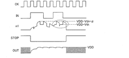
- FIG. 46 is a circuit diagram showing a configuration of the semiconductor device of Patent Document 1.
- This semiconductor device is composed of an n-type MOS transistor.
- the semiconductor device 100 includes four n-type MOS transistors T101 to T104 and a capacitor C101.
- the transistor T101 has a drain terminal connected to the power supply VDD and a gate terminal connected to the input terminal IN.
- the transistor T103 has a source terminal connected to the power supply VSS and a gate terminal to which a STOP signal (control signal) is input.
- the transistor T102 has a drain terminal connected to the clock terminal ⁇ and a gate terminal connected to the source terminal of the transistor T101 and the drain terminal of the transistor T103.
- the transistor T104 has a drain terminal connected to the source terminal of the transistor T102, a source terminal connected to the power supply VSS, and a gate terminal connected to the gate terminal of the transistor T103.
- a connection point between the transistors T101, T102, and T103 is a node N1
- a connection point between the transistors T102 and T104 is a node N2.
- a capacitor C101 is provided between the node N1 and the node N2.
- Node N2 is connected to output terminal OUT.
- FIG. 47 is a timing chart showing waveforms of various signals in the semiconductor device 100.
- the transistor T101 When the input signal IN becomes high level, the transistor T101 is turned on, and the potential of the node N1 becomes VDD ⁇ Vth when the threshold voltage of the transistor T101 is Vth (precharge operation). When the potential of the node N1 rises, the transistor T102 is turned on. When the clock signal ⁇ is at a low level, a low-level signal is output from the output terminal OUT. The potential of the node N1 is held (floating state) once the charge is precharged until the STOP signal becomes active (high level). When the clock signal ⁇ becomes high level in this floating state, the potential of the node N1 is increased by the ⁇ potential by the capacitor C101 and becomes VDD ⁇ Vth + ⁇ (bootstrap operation). While this potential exceeds VDD + Vth, a signal having a potential level of VDD is output from the output terminal OUT.
- the node N1 is discharged to VSS by the transistor T103, and the transistor T102 is turned off.
- a signal having a potential level of VSS is output from the output terminal OUT when the transistor T104 is turned on.
- the output signal is affected by off-leakage (a minute current that flows when the transistor is off), and the potential of the semiconductor device gradually decreases. is there. Further, since the output signal becomes high impedance when the potential is lowered and is easily affected by noise, there is a problem that malfunction occurs in a subsequent circuit that receives the output signal. Specifically, for example, when the semiconductor device is used as a scanning signal line selection circuit of a shift register in a liquid crystal display device, if the output signal of the semiconductor device becomes weak against noise, the scanning signal lines are sequentially arranged. There is a possibility that a malfunction occurs such that the selection operation is not accurately performed.
- the precharged node N1 is discharged, and the potential of the node N1 gradually decreases (dotted line of the node N1 in FIG. 47).
- the transistor T102 is turned off when the clock signal ⁇ is at a high level (VDD).
- the output signal of the transistor T102 has a high impedance, and the output signal OUT is easily affected by noise.
- the transistor T102 when the potential of the node N1 is further decreased to be lower than VDD, the transistor T102 is turned off. For example, due to off-leakage of the transistor T104, the output signal OUT itself is indicated by a dotted line in FIG. The potential level also decreases. This may cause a malfunction in the subsequent circuit.
- the potential of the node N1 decreases due to the influence of off-leakage or the like. For example, when the frequency of the clock signal ⁇ is low or the time for holding the charge of the node N1 is long, the potential of the node N1 The potential drop is further increased. Therefore, the output signal has a high impedance and is easily affected by noise.
- the present invention has been made in view of the above problems, and an object of the present invention is to provide a semiconductor device that includes transistors of the same conductivity type and can output a stable signal while preventing a decrease in potential level. It is providing the display apparatus provided with.
- a semiconductor device is a semiconductor device including a plurality of transistors having the same conductivity type, and an on voltage is applied to a first terminal and an input signal is applied to a control terminal. A second voltage is applied to the input first transistor and the first terminal, the second terminal is connected to the output terminal, and the control terminal is connected to the second terminal of the first transistor. And a capacitor provided between a connection point between the first transistor and the second transistor and a clock terminal for inputting a clock signal, and the frequency of the clock signal is from the output terminal. It is characterized by being higher than the frequency of the output signal to be output.
- the transistor includes a first terminal, a second terminal, and a control terminal.
- the transistor conducts the first terminal and the second terminal by a control signal input to the control terminal, and outputs a signal having a desired potential level.
- the control signal here has a voltage (signal level: VDD) that turns the transistor on when supplied to the control terminal, and a voltage (signal level) that turns the transistor off when supplied to the control terminal. : VSS).
- the potential of the node connected to the control terminal of the transistor that outputs a signal having a desired potential level gradually decreases due to the influence of off-leakage or the like.
- a node connected to a control terminal of a transistor that outputs a signal having a desired potential level, that is, a connection point (node) between the first transistor and the second transistor via a capacitor, A clock signal having a frequency higher than that of the output signal is input.
- the potential of the node is first increased by ⁇ potential by the clock signal and the capacitance, and then decreased by, for example, ⁇ potential by off-leakage or the like, and VDD ⁇ Vth + ⁇ .
- the clock signal becomes low level (VSS)
- the node potential becomes VDD ⁇ Vth ⁇ .
- the input signal is high level (VDD)
- the node potential becomes VDD ⁇ Vth. It is charged until.
- the clock signal becomes high level again, the potential of the node is pushed up to VDD ⁇ Vth + ⁇ again.
- the push-up operation is performed according to the cycle of the clock signal having a frequency higher than that of the output signal. Therefore, even when the potential of the node decreases due to off-leakage or the like, the potential can be recovered immediately by the pushing-up operation. As a result, the potential of the node can be increased in a cycle shorter than that of the conventional configuration, so that the potential level of the output signal can be stabilized and the operation of the subsequent circuit that receives the output signal can be stabilized.
- the output signal can be maintained at VDD.
- the output signal can maintain a low impedance and is resistant to noise.
- the semiconductor device includes a third transistor in which the first terminal is connected to the connection point, the off voltage is input to the second terminal, and the control signal is input to the control terminal. It is desirable to have more.
- the potential of the node can be reliably lowered to VSS.
- the first terminal is connected to the output terminal, the off voltage is applied to the second terminal, and the control signal is input to the control terminal. It is desirable to further include.
- the potential of the node can be reliably lowered to VSS and the potential level of the output signal is set to the low level (off voltage). : VSS).
- the fifth transistor has an on-voltage input to the first terminal, a second terminal connected to the connection point, and a control terminal connected to the output terminal. It is desirable to further include.
- the output signal is input to the control terminal of the fifth transistor, the input signal becomes low level while the output signal is outputting high level (ON voltage: VDD).
- the fifth transistor is again charged to VDD-Vth even if the potential of the node is decreased due to off-leakage or the like.
- the semiconductor device further includes a sixth transistor that outputs the input signal in the semiconductor device, and the sixth transistor has a first terminal connected to the input terminal and a second terminal connected to the input terminal.
- the first transistor is connected to the control terminal and the output terminal, and an enable signal is input to the control terminal.
- the control signal of the first transistor is always high level. A signal can be input. Thereby, the active state of the semiconductor device can be stably maintained.
- the first terminal is connected to the connection point, the off voltage is input to the second terminal, and the initial state of the semiconductor device is stabilized at the control terminal. It is desirable to further include a seventh transistor to which the initialization signal is input.
- the potential of the node can be fixed to VSS by inputting a high-level initialization signal to the seventh transistor in the initial state, so that the initial state can be stabilized.
- the first terminal is connected to the clock terminal
- the second terminal is connected to one end of the capacitor
- the input signal is input to the control terminal. It is desirable to further include the transistor.
- the clock terminal and the capacitor connected to the node can be separated by controlling on / off of the eighth transistor.
- the load of the clock terminal can be limited to the parasitic capacitance of the eighth transistor. Therefore, it is possible to reduce power consumption by reducing the driving capability of the circuit that drives the clock terminal and the effect of reducing the capacity.
- a semiconductor device is a semiconductor device including a plurality of transistors having the same conductivity type, and an on voltage is applied to a first terminal and an input signal is applied to a control terminal. A second voltage is applied to the input first transistor and the first terminal, the second terminal is connected to the output terminal, and the control terminal is connected to the second terminal of the first transistor. And a capacitor provided between a connection point between the first transistor and the second transistor and a clock terminal for inputting a clock signal, and a first terminal connected to the connection point for control.
- a tenth transistor having an on-voltage input to the terminal, a first terminal connected to the second terminal of the tenth transistor, an off-voltage input to the second terminal, and a control signal to the control terminal
- the frequency of the clock signal input is characterized in that it is set higher than the frequency of the output signal output from the output terminal.
- the semiconductor device includes a tenth transistor between the node and the third transistor. Accordingly, although details will be described later, for example, the potential applied to the third transistor can be lowered, so that a highly reliable circuit can be configured.
- the clock signal has a waveform that periodically repeats a high level and a low level, and the clock signal is from a high level during one low period. It is desirable to set the period until the potential at the connection point is saturated after changing to the low level.
- a display device includes any one of the above semiconductor devices.
- the display device according to the present invention is preferably a liquid crystal display device.
- FIG. 1 is a circuit diagram illustrating a configuration of a circuit according to a first embodiment.
- 2 is a timing chart showing waveforms of various signals in the circuit shown in FIG. 2 is a timing chart showing waveforms of various signals when affected by off-leakage or the like in the circuit shown in FIG. It is a timing chart which shows the waveform of various signals at the time of being influenced by off-leak etc. in the conventional circuit.
- 2 is a timing chart showing waveforms of various signals when a clock signal ⁇ is input to the drain terminal of a transistor T2 in the circuit shown in FIG.
- FIG. 6 is a circuit diagram illustrating a configuration of a circuit according to a second embodiment. 7 is a timing chart showing waveforms of various signals in the circuit shown in FIG. FIG.
- FIG. 6 is a circuit diagram illustrating a configuration of a circuit according to a third embodiment.
- FIG. 6 is a circuit diagram showing a configuration of a circuit according to a fourth embodiment.
- 10 is a timing chart showing waveforms of various signals in the circuit shown in FIG.
- FIG. 10 is a circuit diagram showing another configuration of the transistor T6 in the circuit shown in FIG.
- FIG. 10 is a circuit diagram showing another configuration of the transistor T6 in the circuit shown in FIG.
- FIG. 10 is a circuit diagram showing a configuration of a circuit according to a fifth embodiment.
- FIG. 10 is a circuit diagram showing a configuration of a circuit according to a sixth embodiment.
- FIG. 15 is a circuit diagram showing another configuration of the circuit shown in FIG. 14.
- FIG. 10 is a circuit diagram showing a configuration of a circuit according to a seventh embodiment.
- FIG. 20 is a circuit diagram showing another configuration of the circuit according to the seventh embodiment.
- FIG. 2 is a circuit diagram showing a configuration when a transistor T1 is diode-connected in the circuit shown in FIG.
- FIG. 7 is a circuit diagram showing a configuration when a transistor T1 is diode-connected in the circuit shown in FIG.
- FIG. 9 is a circuit diagram showing a configuration when a transistor T1 is diode-connected in the circuit shown in FIG.
- FIG. 10 is a circuit diagram showing a configuration when a transistor T1 is diode-connected in the circuit shown in FIG. FIG.
- FIG. 14 is a circuit diagram showing a configuration when a transistor T1 is diode-connected in the circuit shown in FIG.
- FIG. 15 is a circuit diagram showing a configuration when a transistor T1 is diode-connected in the circuit shown in FIG.
- FIG. 17 is a circuit diagram showing a configuration when a transistor T1 is diode-connected in the circuit shown in FIG.
- FIG. 19 is a timing chart showing waveforms of various signals in the circuit shown in FIG. 18. It is a figure which shows the waveform of the clock signal CK in each embodiment of this invention. It is a block diagram which shows the whole structure of the liquid crystal display device which concerns on this Embodiment.
- FIG. 15 is a circuit diagram showing a configuration when a transistor T1 is diode-connected in the circuit shown in FIG.
- FIG. 17 is a circuit diagram showing a configuration when a transistor T1 is diode-connected in the circuit shown in FIG.
- FIG. 19 is a timing chart showing waveforms of various signals
- FIG. 3 is a block diagram illustrating a configuration of a memory circuit provided in the CS driver according to the first embodiment.
- FIG. 29 is a circuit diagram showing a configuration of a memory circuit shown in FIG. 28.
- FIG. 29 is a timing chart showing waveforms of various signals in the memory circuit shown in FIG. 28.
- FIG. FIG. 29 is a circuit diagram showing a configuration of an inverter circuit that generates an inverted signal INB from an input signal IN in the memory circuit shown in FIG. 28.
- FIG. 29 is a circuit diagram showing another configuration of an inverter circuit that generates an inverted signal INB from an input signal IN in the memory circuit shown in FIG. 28.
- FIG. 6 is a block diagram illustrating a configuration of a buffer circuit according to a second embodiment.
- FIG. 34 is a circuit diagram showing a configuration of a buffer circuit shown in FIG. 33.
- FIG. 34 is a block diagram showing a case where the inverter is configured by a bootstrap circuit in the buffer circuit shown in FIG. 33.
- FIG. 36 is a circuit diagram showing a configuration of a buffer circuit shown in FIG. 35.
- FIG. 10 is a block diagram illustrating a configuration of a buffer circuit according to a third embodiment.
- FIG. 38 is a circuit diagram showing a case where the inverter is configured by a bootstrap circuit in the buffer circuit shown in FIG. 37.
- FIG. 10 is a block diagram illustrating a configuration of a buffer circuit according to a fourth embodiment.
- FIG. 40 is a circuit diagram showing a configuration of a buffer circuit shown in FIG. 39.
- FIG. 40 is a circuit diagram showing a configuration of a buffer circuit shown in FIG. 39.
- FIG. 10 is a block diagram illustrating a configuration of a unit circuit constituting a shift register according to a fourth embodiment.
- FIG. 42 is a block diagram showing another configuration of the unit circuit configuring the shift register shown in FIG. 41.
- FIG. 42 is a block diagram showing another configuration of the unit circuit configuring the shift register shown in FIG. 41.
- FIG. 2 is a circuit diagram in the case where the circuit configuration illustrated in FIG. 1 is configured by a p-channel transistor.
- 44 is a timing chart showing waveforms of various signals in the circuit shown in FIG. 44, where (a) in the figure shows a waveform when VSS is input to the source terminal of the transistor T2 ′, and (b) in the figure shows the transistor. The waveform is shown when the clock signal ⁇ is input to the source terminal of T2 ′.
- It is a circuit diagram which shows the structure of the conventional semiconductor device.
- 47 is a timing chart showing waveforms of various signals in the semiconductor device shown in FIG. 46.
- Embodiments of the present invention will be described with reference to FIGS. 1 to 45 as follows.
- An Active signal holding circuit (hereinafter simply referred to as “circuit”) corresponding to the semiconductor device of the present invention is configured using transistors of the same conductivity type, that is, a unipolar channel (n-channel type or p-channel type). Yes.
- a unipolar channel n-channel type or p-channel type.
- the configuration of an n-channel transistor is described as an example, and the configuration of a p-channel transistor is only illustrated at the end of this column, and detailed description is omitted.
- this transistor for example, a TFT and a field effect transistor formed on a silicon substrate can be used.
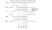
- FIG. 1 is a circuit diagram showing the configuration of the circuit 10
- FIG. 2 is a timing chart showing waveforms of various signals in the circuit 10.
- the circuit 10 includes a transistor T1 (first transistor), a transistor T2 (second transistor), a transistor T3 (third transistor), and a capacitor C1, and the output signal OUT of the circuit 10 is connected to one end of the capacitor C1.
- a clock signal CK having a higher frequency is input.
- the voltage (signal level) that turns the transistor on when applied to the gate terminal (control terminal) is referred to as on-voltage (on level), and the voltage that turns the transistor off when applied to the gate terminal (signal level).
- Signal level is called off voltage (off level).
- a high voltage is an on voltage (high level is an on level)
- a low voltage is an off voltage (low level is an off level)
- vice versa for a p-channel transistor In an n-channel transistor, a high voltage is an on voltage (high level is an on level), a low voltage is an off voltage (low level is an off level), and vice versa for a p-channel transistor.
- the transistor T1 has a drain terminal (first terminal) connected to the power supply VDD and a gate terminal (control terminal) connected to the input terminal IN.
- the transistor T2 has a drain terminal (first terminal) connected to the power supply VDD, a gate terminal (control terminal) connected to the source terminal of the transistor T1, and a source terminal (second terminal) connected to the output terminal OUT.
- the transistor T3 has a drain terminal (first terminal) connected to the source terminal of the transistor T1 and the gate terminal of the transistor T2, and is connected to the clock terminal CK via the capacitor C1.
- a connection point between the transistors T1, T2, T3, and the capacitor C1 is a node n1.
- the circuit 10 of the present embodiment receives a clock signal CK having a higher frequency than the output signal OUT at one end of the capacitor C1.
- the other end of C1 is connected to a node n1 that holds a high level signal in a floating state.
- the transistor T1 When the input signal IN becomes high level (VDD), the transistor T1 is turned on, and the potential of the node n1 becomes VDD ⁇ Vth when the threshold voltage of the transistor T1 is Vth (precharge operation). When the potential of the node n1 rises, the transistor T2 is turned on.
- the input signal IN changes from a high level to a low level (VSS)
- the node n1 When the clock signal CK becomes high level, the potential of the node n1 is increased by the ⁇ potential by the clock signal CK and becomes VDD ⁇ Vth + ⁇ .
- this potential exceeds VDD + Vth the transistor T2 outputs VDD to the output terminal OUT.
- the transistor T3 is turned on, the charge of the node n1 is discharged, and the transistor T2 is turned off. As a result, the output terminal OUT enters a floating state (shaded area in FIG. 2).
- the potential decreases due to the influence of off-leakage or the like of the transistor T3 and the like until the potential of the node n1 pushed up by the clock signal CK becomes lower than VDD + Vth.
- the VDD is normally output from the output terminal OUT.
- FIG. 3 is a timing chart showing waveforms of various signals when the circuit 10 is affected by off-leakage or the like.
- FIG. 4 is a timing chart showing waveforms of various signals when the conventional circuit shown in FIG. 46 is affected by off-leakage or the like.
- VDD ⁇ Vth + ⁇ when the potential of the node n1 is pushed up by the clock signal CK and then drops by ⁇ potential due to leakage, VDD ⁇ Vth + ⁇ is obtained. After that, when the clock signal CK becomes low level, the potential of the node n1 becomes VDD ⁇ Vth ⁇ . However, if the input signal IN is high level here, the potential of the node n1 reaches VDD ⁇ Vth. Charged. Therefore, when the clock signal CK becomes high level again, the potential of the node n1 is pushed up to VDD ⁇ Vth + ⁇ (portion surrounded by a dotted line in FIG. 3).
- the output signal OUT can maintain a low impedance and is resistant to noise.
- the potential of the node n1 can be charged again to VDD ⁇ Vth. Since the frequency of the clock signal CK is set higher than the frequency of the output signal, the potential of the node n1 is again increased to VDD + Vth or more by the push-up operation by the clock signal CK until the STOP signal becomes high level. Can be pushed up. Accordingly, it is possible to ensure a period during which VDD can be output and a period during which the impedance is low as compared with the conventional case.
- the amplitude of the clock signal CK and the capacitance C1 are set such that the potential (VDD ⁇ Vth + ⁇ ) of the pushed-up node n1 is equal to or higher than VDD + Vth.
- FIG. 5 is a timing chart showing waveforms of various signals in the configuration of the circuit 10 when the clock signal ⁇ is input to the drain terminal of the transistor T2.
- the potential level of the signal input to the transistor T2 can be output, the potential of the clock signal ⁇ is turned on when the transistor T2 is turned on. The level is output.
- FIG. 6 is a circuit diagram showing the configuration of the circuit 20
- FIG. 7 is a timing chart showing waveforms of various signals in the circuit 20.
- members having the same functions as those shown in the first embodiment are given the same reference numerals, and explanation thereof is omitted.
- the terms defined in Embodiment 1 are used in accordance with the definitions in this embodiment unless otherwise specified.
- the output terminal OUT is in a floating state (hatched line in FIG. 2) at the timing when the STOP signal becomes high level and the node n1 becomes low level potential. Therefore, it is easily affected by noise and the like.
- the circuit 20 of this embodiment further includes a transistor T4 (fourth transistor) in the circuit 10.
- the transistor T4 has a drain terminal (first terminal) connected to the source terminal and the output terminal OUT of the transistor T2, a source terminal (second terminal) connected to the power supply VSS, and a gate terminal. (Control terminal) is connected to the gate terminal of the transistor T3.
- the gate terminals of the transistors T3 and T4 are connected to the input terminal IN2, and an input signal IN2 for controlling on / off of the transistors T3 and T4 is input.
- a connection point between the transistors T2 and T4 and the output terminal OUT is a node n2.
- the transistors T3 and T4 are turned on by inputting the high-level input signal IN2 at the timing when the node n1 becomes the low-level potential.
- the electric charge of n1 can be surely discharged and the potential level of the output signal OUT can be fixed to the low level (VSS).
- the signal input to the gate terminal of the transistor T4 is not particularly limited as long as the potential level of the output signal OUT can be fixed to a low level (VSS), and another control signal may be input.
- VSS low level
- FIG. 8 is a circuit diagram showing a configuration of the circuit 30.
- members having the same functions as those shown in the first and second embodiments are given the same reference numerals, and explanation thereof is omitted.
- the terms defined in Embodiments 1 and 2 are used in accordance with the definitions in this embodiment unless otherwise specified.
- the circuit 30 of the present embodiment further includes a transistor T5 (fifth transistor) that plays a role of a refresh function in the circuit 20 shown in FIG.
- the transistor T5 has a drain terminal (first terminal) connected to the power supply VDD, a source terminal (second terminal) connected to the node n1, and a gate terminal (control terminal) connected to the node n2. Connected to.
- the output signal OUT is input to the gate terminal of the transistor T5, the input signal IN1 is at a low level and the transistor T1 is off while the output signal OUT is at a high level.
- the transistor T5 is charged again to VDD-Vth (refresh operation).
- the potential of the node n1 can be pushed up to VDD ⁇ Vth + ⁇ during the period when the clock signal CK outputs a high level. Therefore, the output signal OUT can stably output VDD, and can operate normally without malfunction during low frequency operation.
- FIG. 9 is a circuit diagram showing the configuration of the circuit 40
- FIG. 10 is a timing chart showing waveforms of various signals in the circuit 40.
- members having the same functions as those shown in the first to third embodiments are given the same reference numerals, and explanation thereof is omitted.
- the terms defined in Embodiments 1 to 3 are used in accordance with the definitions in this embodiment unless otherwise specified.
- a transistor T6 (sixth transistor) is further provided between the input terminal IN1 and the transistor T1.
- the transistor T6 has a drain terminal (first terminal) connected to the input terminal IN1, a source terminal (second terminal) connected to the gate terminal of the transistor T1, and a gate terminal (control terminal). ) Is input with an enable signal EN.
- the source terminal of the transistor T6 is also connected to a connection point (node n2) between the transistors T2 and T4.
- the circuit 40 can be kept in the active state.
- the transistor T1 since the output terminal OUT and the gate terminal of the transistor T1 are connected to each other, the transistor T1 is turned on when the potential of the node n1 is equal to or lower than VDD ⁇ Vth while the output signal OUT is at a high level. become. Note that when the potential of the node n1 is equal to or higher than VDD ⁇ Vth, the transistor T1 is turned off and the node n1 is in a floating state.
- the potential of the node n1 is charged again to VDD-Vth by the transistor T1 (refresh operation) even if it drops due to off-leakage or the like.
- the potential of the node n1 can be pushed up to VDD ⁇ Vth + ⁇ , so that the output signal OUT can stably output VDD, It can operate normally without malfunction during low frequency operation.
- the transistor T6 is not limited to the configuration of FIG. 9 described above, and other configurations include, for example, a configuration in which the source terminal floats when the input signal IN1 becomes a low level potential. Includes the configuration shown in FIG. 11 and the configuration shown in FIG. 12.
- the power supply VDD is connected to the drain terminal of the transistor T6, and the input signal IN1 is input to the gate terminal.
- the input signal IN1 is input to the drain terminal and the gate terminal of the transistor T6.
- the active state is maintained even if the input signal IN1 subsequently becomes low level. Suitable for configuration.
- FIG. 13 is a circuit diagram showing a configuration of the circuit 50.
- members having the same functions as those shown in Embodiments 1 to 4 are given the same reference numerals, and explanation thereof is omitted. Further, the terms defined in Embodiments 1 to 4 are used in accordance with the definitions in this embodiment unless otherwise specified.
- the circuit 50 of the present embodiment further includes a transistor T7 (seventh transistor) in each of the circuits shown in the first to fourth embodiments.
- the circuit 50 shown in FIG. 13 has a configuration in which the transistor T7 is provided to the circuit 10 shown in FIG. 1, and the transistor T7 receives the initialization signal INI at the gate terminal (control terminal) and the source terminal (first terminal). 2 terminal) is connected to the power supply VSS, and the drain terminal (first terminal) is connected to the node n1.
- the potential of the node n1 can be fixed to VSS, so that the initial state can be stabilized.
- the initial state can be stabilized for each circuit of the second to fourth embodiments by providing the transistor T7 as described above.
- FIG. 14 is a circuit diagram showing the configuration of the circuit 60.
- members having the same functions as those shown in the first to fifth embodiments are given the same reference numerals, and the explanation thereof is omitted. Is omitted. Further, the terms defined in Embodiments 1 to 5 are used in accordance with the definitions in this embodiment unless otherwise specified.
- the circuit configurations shown in the first to fifth embodiments have a problem that the capacity of the clock terminal CK increases.
- a specific example of the clock load will be described using the circuit 10 of FIG. 1 as an example.
- the capacity of the clock terminal CK increases during the period when the node n1 is not in the floating state.
- the capacity becomes very large.
- the circuit 60 of this embodiment further includes a transistor T8 (eighth transistor) in each of the circuits shown in the first to fifth embodiments.
- a circuit 60 shown in FIG. 14 has a configuration in which a transistor T8 is provided to the circuit 10 shown in FIG. 1, and the transistor T8 has a gate terminal (control terminal) connected to the input terminal IN and a drain terminal (first terminal). Terminal) is connected to the clock terminal CK, and the source terminal (second terminal) is connected to the node n1 through the capacitor C1.
- the node T1 is not in a floating state by the transistor T8, and the clock terminal CK and the capacitor C1 can be disconnected during a period when the load on the clock terminal CK becomes very large.
- the node n1 when the potential of the node n1 is fixed to VSS, the node n1 does not need to be pushed up from the clock signal CK. Therefore, the period between the clock terminal CK and the capacitor C1 is electrically connected by the transistor T8. As a result, the load on the clock terminal CK becomes only the parasitic capacitance of the transistor T8 and thus becomes very small.
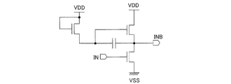
- an inverter 6 including a resistor R1 and a transistor T11 may be provided.
- the transistor T9 has a drain terminal connected to the node n3, a source terminal connected to the power supply VSS, and a gate terminal connected to the input terminal IN to the inverter 6.
- a signal input to the gate terminal is not particularly limited, and is one period during which the potential of the node n1 is fixed at VSS.
- Other control signals that turn off the transistor T8 may be input during the period or period.
- the inverted signal of the input terminal IN is generated by the inverter 6 and output to the input terminal INB.
- the inverted signal of the signal input to the input terminal IN exists as another control signal.
- the signal may be input to the input terminal INB.
- the power consumption consumed by the capacitor is reduced.
- the clock signal CK is present during a period in which the potential of the node n1 in the circuit 10 is fixed to VSS by an external clock operation, for example.
- a configuration may be adopted in which the frequency is fixed to a DC level or the frequency of the clock signal CK is reduced in order to reduce power consumption.
- FIG. 16 is a circuit diagram showing a configuration of the circuit 70.
- members having the same functions as those shown in the first to sixth embodiments are given the same reference numerals and explanations thereof are omitted. Is omitted. Further, the terms defined in Embodiments 1 to 6 are used in accordance with the definitions in this embodiment unless otherwise specified.
- the transistor connected to the node n1 is connected between the gate and the source.
- a high voltage is applied between the gate and the drain and between the source and the drain. In some cases, the transistor exceeds its own withstand voltage, and there is a risk of being destroyed.
- a high voltage is applied particularly between the gate and drain and between the source and drain of the transistor T3.
- VDD ⁇ Vth + ⁇ the voltage between the gate and the drain and between the source and the drain of the transistor T3 is VDD ⁇ Vth + ⁇ VSS.
- VDD 10V
- VSS ⁇ 10V
- ⁇ 15V
- VDD-Vth + ⁇ -VSS 35V-Vth It becomes.
- a potential difference of 20 V between VDD and VSS is applied to other nodes.
- a high voltage is applied to the transistor connected to the node n1.
- the circuit 70 of this embodiment further includes a transistor T10 (tenth transistor) in each of the circuits shown in the first to sixth embodiments.
- a circuit 70 illustrated in FIG. 16 includes a transistor T10 with respect to the circuit 10 illustrated in FIG. 1.
- the transistor T10 includes a gate terminal (control terminal) connected to the power supply VDD and a drain terminal (first terminal). Terminal) is connected to the node n1, and the source terminal (second terminal) is connected to the drain terminal of the transistor T3.
- a connection point between the transistors T3 and T10 is a node n4.
- FIG. 17 is an example thereof, and shows a configuration when applied to the circuit shown in FIG. 15 of the sixth embodiment.
- the drain terminal of the transistor T1 is connected to the power supply VDD.
- the configuration of the circuit of the present invention is not limited to this, and may be a so-called diode-connected configuration in which the drain terminal and the gate terminal of the transistor T1 are connected to each other.
- 18 to 24 show the circuits 11, 21, 31, 41, 51, 61, and 71 when the transistor T1 is diode-connected in the circuits 10, 20, 30, 40, 50, 60, and 70, respectively. It is a circuit diagram which shows a structure.
- the transistor T1 is configured as in the circuit 10
- the transistor T3 when the transistor T3 is in an on state and a low level is input to the input terminal IN and the noise is generated in the input signal, the transistor T1 is instantaneously
- a through current flows from the power supply VDD to the power supply VSS via the transistors T1 and T3, resulting in an increase in current consumption or a malfunction.
- the gate terminal and the drain terminal of the transistor T1 are connected, even if noise occurs in the input terminal IN and the transistor T1 is turned on, the source ⁇
- the potential difference between the drains is only the potential of noise, and the through current is reduced because the potential difference is small compared to the case where the power supply VDD is connected to the drain terminal.
- the transistor T3 since the transistor T3 is in the on state, even if the transistor T1 is turned on due to noise, the potential changed by the noise of the input terminal IN is pulled to the power supply VSS via the transistor T3. The action of turning off works. Therefore, malfunction of the transistor T1 due to the influence of noise can be prevented.
- FIG. 25 is a timing chart showing waveforms of various signals in the circuit 11 shown in FIG. 18 among the circuits when the transistor T1 is diode-connected. As shown in FIG. 25, since the potential level of the signal input to the drain terminal of the transistor T2 can be output as in the configuration of the circuit 10 shown in FIG. Is output.
- the configuration in which the clock signal ⁇ is input to the drain terminal of the transistor T2 has been described. However, this configuration can also be applied to the circuit described in each embodiment. When turned on, the potential level of the clock signal ⁇ is output.
- the clock signal CK input to the Active signal holding circuit of the present invention has a waveform in which a high level and a low level are periodically repeated.
- the output signal OUT of the Active signal holding circuit has a particularly low impedance when the clock signal CK is at a high level (period T). Therefore, as shown in FIG. 26, when the duty ratio of the clock signal CK is 50%, for example, the output signal OUT has a low impedance during this 50% period. That is, the low impedance period of the output signal OUT can be adjusted by adjusting the duty ratio of the clock signal CK.
- a preferable value for the duty ratio of the clock signal CK is examined with reference to the configuration of FIG.
- the clock signal CK becomes low level
- the potential of the node n1 decreases due to off-leakage or the like, and becomes VDD ⁇ Vth ⁇ .
- the high period: low period T1 ⁇ t ⁇ : t ⁇ is an ideal duty ratio.
- the period during which the clock signal CK shifts from the high level to the low level is determined by the time constant of the load (capacitance and resistance) of the clock CK terminal.
- the duty ratio of the clock signal is such that the low level period of one cycle of the clock signal CK is the period until the potential of the node n1 is saturated after the clock signal CK changes from the high level to the low level. It is preferable to set so as to be.
- the duty ratio is preferably set so that the low impedance period of the transistor T2 is longer.
- the transition time in the clock signal CK exceeds 50%, the transition to the next high level is ensured without being at the low level after the transition. Therefore, in order to obtain the push-up voltage ⁇ , the capacitance C1 is further increased. It is necessary to correct (correct). As a result, the circuit scale becomes large, or the capacity load increases, so that the transition time is further increased. In order to avoid this, the transition time is generally within 50% by slowing the frequency of the clock signal or by designing the load to be driven by the clock signal CK to be small.
- the duty ratio is preferably 50% or more so that the period of low impedance is as long as possible.
- the clock signal CK_H in FIG. 26 is an example of a waveform when the high-level period T is lengthened (duty ratio is increased). This makes it possible to lengthen the low impedance period of the output signal OUT of the Active signal holding circuit. And since the period of low impedance can be lengthened, it becomes more resistant to noise and the load can be driven quickly. Thus, it is preferable that the clock signal CK has a higher frequency than the output signal OUT and has a high level (active side potential) period.
- FIG. 27 is a block diagram showing the overall configuration of the liquid crystal display device.
- the liquid crystal display device 151 includes a pixel region 153, a source driver 154, a gate / CS driver 155, a BUFF / level shifter circuit 156, a power supply circuit 157, and a terminal 158 on the panel 152.
- the source driver 154 includes an output circuit 154 a and outputs a data signal to each source bus line in the pixel region 153.
- the gate / CS driver 155 includes an output circuit 155a, outputs a selection signal to the gate bus line in order to write a data signal from the source driver 154 to each pixel in the pixel region 153, and each pixel in the pixel region 153 A CS signal is output to the CS bus line in order to increase the write potential.
- the output circuits 154a and 155a are composed of a buffer which is an amplifier circuit with a low output impedance that generates a data signal of the same magnification from the input signal.
- the BUFF / level shifter circuit includes buffers that are low output impedance amplifier circuits such as an equal-amplifier circuit that corrects signal attenuation such as an inverter and a level shifter circuit that converts a power supply voltage level of the signal.
- the signal passed through is supplied to the source driver 154 and the gate driver 155.
- the power supply circuit 157 generates a logic circuit power supply, a reference voltage of the data signal, a counter voltage, an auxiliary capacitance voltage, and the like.
- Terminals 158... Are terminals for inputting signals and power to the above-described circuits on the panel 152.
- the liquid crystal display device may be configured by a demultiplexer instead of the source driver.
- Each circuit shown in the first to seventh embodiments can be applied to each part in the liquid crystal display device 151.
- a memory circuit provided in a CS driver Example 1
- an example applied to a buffer circuit and a level shifter circuit Examples 2 to 4
- an example applied to a shift register Example 1 Example 5
- FIG. 28 is a block diagram showing a configuration of the memory circuit 1 provided in the CS driver in the present embodiment
- FIG. 29 is a circuit diagram of the memory circuit 1.
- FIG. 30 is a timing chart showing waveforms of various signals in the memory circuit 1.
- the memory circuit 1 includes the two circuits (Active signal holding circuits) described in the above embodiments. Specifically, in the memory circuit 1, for example, the STOP terminal of one circuit 10 (denoted as the circuit 10b) shown in FIG. 1 and the output terminal OUT of the other circuit 10 (denoted as the circuit 10a) are connected. It is constituted by.
- the memory circuit only needs to have at least the configuration of the circuit 10 shown in FIG. 1.
- the transistor T4 in addition to the configuration of the circuit 10, the transistor T4 (transistors Ta4 and Tb4 in FIG. 28). And includes the configuration of the circuit 20 shown in FIG.
- the circuit 10a to which a high-level signal is input is in an active state, and the node na1 holds charges while the clock signal is input. Therefore, the output signal OUT of VDD is output from the circuit 10a as described in the above embodiments. The output signal OUT is input to the STOP terminal (FIG. 29) of the other circuit 10b.
- the circuit 10b in which the VDD signal is input to the STOP terminal becomes inactive, and VSS is output from the transistor Tb4. Since IN and INB have opposite polarities, when one outputs VDD, the other outputs VSS. Thus, while the clock signal CK is being input, the potentials of the circuits 10a and 10b are held until the next enable signal EN becomes high level.
- the inverted signal INB of the input signal IN is input from the outside.
- the configuration is not limited to this, and other configurations are shown in FIGS. 31 and 32, for example.
- the inverter circuit may be configured in the memory circuit 1 to generate the inverted signal INB from the input signal IN.
- FIG. 31 shows an inverter constituted by a resistor R1 and a transistor T11
- FIG. 32 shows an inverter constituted by a bootstrap circuit. According to these configurations, when the input signal IN is at a high level (VDD), a low level (VSS) signal is output as the inverted signal INB, and when the input signal IN is at a low level (VSS), the high level is output.
- the signal (VDD) is output as the inverted signal INB.
- the transistor T7 shown in the fifth embodiment may be provided in each of the circuits 10a and 10b in order to stabilize the initial state.
- the initialization signal INI is input to the gate terminal
- the respective drain terminals are connected to the node na1 and the node nb1
- the respective source terminals are the power supply VSS and the power supply Connected to each of VDD.
- the memory circuit 1 since the memory circuit 1 has the refresh function described in the above embodiment, it is possible to normally hold a value even at low frequency driving.
- the memory circuit 1 configured by the circuit 20 of the second embodiment has been described.
- the memory circuit 1 according to another embodiment for example, the circuit 30, 40, or 50
- the same effect can be obtained.
- FIG. 33 is a block diagram showing a configuration of the buffer circuit 2 in the present embodiment
- FIG. 34 is a circuit diagram of the buffer circuit 2.
- the buffer circuit 2 includes the circuit (Active signal holding circuit) shown in each of the above embodiments. Specifically, the buffer circuit 2 only needs to have at least the configuration of the circuit 10 shown in FIG. 1.
- a transistor T4 is provided in addition to the configuration of the circuit 10, and FIG. 6 includes the configuration of the circuit 20 shown in FIG.
- the inverter that generates the signal INB input to the circuit 10 is composed of a resistor R1 and a transistor T11. Therefore, when the input signal IN of the inverter is at a high level, a steady current (through current) flows from the power supply VDD to the power supply VSS, and power consumption increases. Therefore, in order to reduce power consumption, it is conceivable to configure the resistor R to have a high resistance. However, in this case, there arises a problem that the drive capability is lowered and a new problem that the resistance becomes weak against noise. .
- the buffer circuit 2 of the present embodiment since the output terminal INB of the inverter is connected only to the gate terminal of the transistor T1 of the circuit 10, the load becomes very small. Therefore, even if the drive capability of the inverter is reduced (even if the resistor R1 is set to a high resistance), the load at the gate terminal of the transistor T1 can be driven quickly, so that high-speed operation is possible and operation of the circuit 10 As a result, the driving capability of the buffer circuit 2 itself can be increased. Therefore, according to the above configuration, a buffer circuit with low power consumption and high driving capability can be configured.
- buffer circuit 2 comprised by the circuit 20 of the said Embodiment 2 was demonstrated in the present Example, you may comprise by the circuit (for example, circuit 30, 40 or 50) in other embodiment. In these configurations, the same effect can be obtained.
- the level shifter Functions as a circuit.
- the inverter may be configured by a bootstrap circuit. Also in this configuration, when the input signal IN is at a high level, a steady current (through current) flows from the power supply VDD to the power supply VSS through the transistors T12 and T13, and power consumption increases. Therefore, in order to reduce power consumption, it is conceivable to reduce the size of the transistors T12 and T13. In this case, however, the problem is that the driving capability is reduced, as in the case of an inverter using resistors, and noise. A new problem of weakening.
- FIG. 37 is a circuit diagram showing a configuration of the buffer circuit 3 in the present embodiment.
- the buffer circuit 3 includes an inverter shown in FIG. 31 and a configuration obtained by modifying the circuit 20 shown in FIG. Specifically, in the circuit 20 shown in FIG. 6, the transistor T3 is omitted, and the transistor T1 has a gate terminal connected to the power supply VDD and a drain terminal connected to the output terminal INB of the inverter. The gate terminal of the transistor T3 is connected to the input terminal IN of the inverter.
- the inverted signal INB becomes VDD.
- the inverted signal INB of VDD is input to the transistor T1
- the potential of the node n1 is charged to VDD ⁇ Vth
- the potential of the node n1 rises to VDD ⁇ Vth + ⁇ by the push-up operation by the clock signal CK. Since the node n1 is connected to the gate terminal of the transistor T2, the potential of the output signal OUTB is VDD with no threshold drop.
- the inverted signal INB becomes VSS, and the potential of the node n1 is discharged to VSS.
- the transistor T3 is turned on, and the potential of the output signal OUTB becomes VSS.
- the transistor T2 when the potential of the node n1 is high due to the push-up operation of the clock signal CK, the transistor T2 has low impedance, so that it is resistant to noise and can drive the load quickly.
- the transistor T3 for discharging the node n1 is not necessary, so that the circuit scale can be reduced.
- the buffer circuit 3 of the present embodiment when the voltage of the input signal IN is input with a voltage other than VDD / VSS (for example, when the High voltage is lower than VDD and the Low voltage is VSS), Functions as a level shifter circuit.
- the inverter may be constituted by a bootstrap circuit as in the second embodiment.
- FIG. 38 is a circuit diagram showing a configuration of a buffer circuit including an inverter configured by a bootstrap circuit.
- the buffer circuit 2 of the second embodiment can operate normally even when the input signal IN becomes a DC signal.
- the buffer 3 of the third embodiment when the input signal IN becomes a DC signal, the voltage at the gate terminal of the transistor T12 becomes VDD ⁇ Vth due to off-leakage. Therefore, since the voltage at the output terminal of the inverter is VDD-2 ⁇ Vth, the node n1 is VDD-2 ⁇ Vth. Although the potential of the node n1 becomes VDD ⁇ 2 ⁇ Vth + ⁇ due to the rising of the clock signal CK, if the capacitor C1 is set so that it becomes larger than VDD + Vth, it operates normally even if the input signal IN becomes a DC signal. Is possible.
- FIG. 39 is a block diagram showing the configuration of the buffer circuit 4 in the present embodiment
- FIG. 40 is a circuit diagram of the buffer circuit 4.
- the buffer circuit 4 includes the inverter shown in FIG. 31 and the circuit 10 shown in FIG. Specifically, as shown in FIG. 40, the output terminal INB of the inverter is connected to the gate terminal of the transistor T1 and the output terminal OUTB of the buffer circuit 4, and the gate terminal of the transistor T3 is connected to the input terminal IN of the inverter. Connected.
- the buffer circuit 4 of the present embodiment when the input signal IN of the inverter is at a low level, the inverted signal INB is output from the high resistance R1, and thus becomes the high impedance VDD, but the output signal of the circuit 10 (transistor The output signal OUTB can obtain a low impedance VDD.
- the buffer circuit 4 since the output terminals INB and OUTB are connected to each other, even when the clock signal CK is stopped, it is possible to output a signal having a potential of VDD that does not drop the threshold value.
- the buffer circuit 4 of this embodiment when the voltage of the input signal IN is input with a voltage other than VDD / VSS (for example, when the High voltage is lower than VDD and the Low voltage is VSS), Functions as a level shifter circuit.
- the buffer circuit 4 of this embodiment can operate normally even when the input signal IN becomes a DC signal, like the buffer circuits 2 and 3 of the second and third embodiments.
- the input signal IN and the inverted signal INB may be interchanged.
- FIG. 41 is a block diagram showing the configuration of the unit circuit 5 constituting the shift register in this embodiment.
- the shift register is configured by cascade-connecting unit circuits 5 shown in FIG. 41.
- the unit circuit 5 is configured to include the circuit (Active signal holding circuit) 10 shown in the first embodiment.
- a conventional configuration can be applied to the configuration excluding the circuit 10.
- the output signal of the circuit 10 is fed back to the input side of the circuit 10. Accordingly, since the node n5 can be held at a high level that is not in a floating state, the disabled state of the shift register can be held. Therefore, the problem with respect to leakage and noise can be solved.
- the clock signal CK1 is input to the clock terminal CK of the even-numbered unit circuit 5 among the clock signals CK1 and CK2 that do not become high level at the same time.
- the clock signal CK2 is input to the clock terminal CK of the unit circuit 5 in the stage, the input signal On-1 is an output signal from the unit circuit 5 in the previous stage, and the input signal On + 1 is an output signal from the unit circuit 5 in the subsequent stage.
- the transistor T1 is turned on, and electric charge is stored in the capacitor C1. Thereafter, every time the clock signal CK is input, the potential of the output signal OUT is raised to VDD through the transistor T2, so that the potential of the node n5 does not decrease due to off-leakage or the like. Then, since the output signal OUT of VDD is fed back to the input terminal IN, the potential of the node n5 is held at VDD until the input signal On-1 next becomes the high level.
- the circuit (Active signal holding circuit) in the present embodiment to the conventional shift register, the potential of the node n5 that has been lowered due to a drop in threshold value, leakage, or the like can be reliably ensured. It can be held at VDD.
- the shift register configured by the circuit 10 of the first embodiment has been described.
- the shift register may be configured by a circuit in another embodiment. In these configurations, the same effect can be obtained.
- the configuration of the shift register to which the circuit in this embodiment can be applied is not particularly limited.
- the unit circuit of each stage in the shift register does not use the output signal of the subsequent unit circuit, that is, the A configuration in which a reset signal is generated in a unit circuit of a stage can be given.
- the disabled state can be maintained.
- the clock signals CK1 and CK2 that do not simultaneously become high in any unit circuit, the clock signal CK1 is input to the clock terminal CK of the even-numbered unit circuit, and the clock signal CK2 is input to the clock terminal CKB.
- the clock signal CK2 is input to the clock terminal CK of the odd-numbered unit circuit 5, the clock signal CK1 is input to the clock terminal CKB, and the input signal On-1 is the output signal of the unit circuit 5 of the previous stage. It is.
- the circuit 10 holds the potential of the node n5 at VDD until the next time the input signal On-1 becomes high level.
- FIG. 44 is a circuit diagram of a circuit 10 ′ when the configuration of the circuit 10 is configured by p-channel transistors.
- FIG. 45 is a timing chart showing waveforms of various signals in the circuit 10 ′.
- FIG. 45A shows a waveform when VSS is input to the drain terminal of the transistor T2 ′, and FIG. ) Shows a waveform when the clock signal ⁇ is input to the drain terminal of the transistor T2 ′.
- the output signal can be stabilized as in the case of the circuit configured by the n-channel transistor described above.
- the semiconductor device includes a capacitor provided between a connection point between the first transistor and the second transistor and a clock terminal that inputs a clock signal, and the clock signal This frequency is higher than the frequency of the output signal output from the output terminal.
- the display device according to the present invention includes the semiconductor device.
- a semiconductor device that includes transistors of the same conductivity type, can output a stable signal while preventing a decrease in potential level, and a display device including the semiconductor device.
- the present invention is a circuit that can stably output without lowering the potential level of an input signal, it can be suitably applied particularly to a display device.
Abstract
Description
2,3,4 バッファ回路
5 (シフトレジスタの)単位回路
10,20,30,40,50,60,70 回路(半導体装置)
11,21,31,41,51,61,71 回路(半導体装置)
T1 トランジスタ(第1のトランジスタ)
T2 トランジスタ(第2のトランジスタ)
T3 トランジスタ(第3のトランジスタ)
T4 トランジスタ(第4のトランジスタ)
T5 トランジスタ(第5のトランジスタ)
T6 トランジスタ(第6のトランジスタ)
T7 トランジスタ(第7のトランジスタ)
T8 トランジスタ(第8のトランジスタ)
T9 トランジスタ(第9のトランジスタ)
T10 トランジスタ(第10のトランジスタ)
151 液晶表示装置(表示装置)
n1,n2,n3,n4,n5,n6 ノード
100 半導体装置
本実施の形態における回路10の構成について、以下に説明する。図1は回路10の構成を示す回路図であり、図2は回路10における各種信号の波形を示すタイミングチャートである。
本実施の形態における回路20の構成について、以下に説明する。図6は回路20の構成を示す回路図であり、図7は回路20における各種信号の波形を示すタイミングチャートである。なお、説明の便宜上、上記実施の形態1において示した部材と同一の機能を有する部材には、同一の符号を付し、その説明を省略する。また、実施の形態1において定義した用語については、特に断わらない限り本実施の形態においてもその定義に則って用いるものとする。
本実施の形態における回路30の構成について、以下に説明する。図8は回路30の構成を示す回路図である。なお、説明の便宜上、上記実施の形態1及び2において示した部材と同一の機能を有する部材には、同一の符号を付し、その説明を省略する。また、実施の形態1及び2において定義した用語については、特に断わらない限り本実施の形態においてもその定義に則って用いるものとする。
本実施の形態における回路40の構成について、以下に説明する。図9は回路40の構成を示す回路図であり、図10は回路40における各種信号の波形を示すタイミングチャートである。なお、説明の便宜上、上記実施の形態1~3において示した部材と同一の機能を有する部材には、同一の符号を付し、その説明を省略する。また、実施の形態1~3において定義した用語については、特に断わらない限り本実施の形態においてもその定義に則って用いるものとする。
本実施の形態における回路50の構成について、以下に説明する。図13は回路50の構成を示す回路図である。なお、説明の便宜上、上記実施の形態1~4において示した部材と同一の機能を有する部材には、同一の符号を付し、その説明を省略する。また、実施の形態1~4において定義した用語については、特に断わらない限り本実施の形態においてもその定義に則って用いるものとする。
本実施の形態における回路60の構成について、以下に説明する。図14は回路60の構成を示す回路図であり、なお、説明の便宜上、上記実施の形態1~5において示した部材と同一の機能を有する部材には、同一の符号を付し、その説明を省略する。また、実施の形態1~5において定義した用語については、特に断わらない限り本実施の形態においてもその定義に則って用いるものとする。
1/クロック端子CKの容量=1/C1+1/Ctr・・・(1)
となる。なお、説明の便宜上、配線負荷等は省略している。
クロック端子CKの容量=1/3×C1
となる。
クロック端子CKの容量=C1
となる。
本実施の形態における回路70の構成について、以下に説明する。図16は回路70の構成を示す回路図であり、なお、説明の便宜上、上記実施の形態1~6において示した部材と同一の機能を有する部材には、同一の符号を付し、その説明を省略する。また、実施の形態1~6において定義した用語については、特に断わらない限り本実施の形態においてもその定義に則って用いるものとする。
VDD-Vth+α-VSS=35V-Vth
となる。これに対して、他のノードでは、VDDとVSSとの電位差20Vが印加される。このように、ノードn1に接続されるトランジスタには高電圧が印加される。
VDD-Vth-VSS=20V-Vth
となり、回路10の場合と比較して、α電位分、印加電圧が低くなる。
図28は、本実施例におけるCSドライバ内に設けられるメモリ回路1の構成を示すブロック図であり、図29は該メモリ回路1の回路図である。図30は、メモリ回路1における各種信号の波形を示すタイミングチャートである。メモリ回路1は、上記各実施の形態に示した2つの回路(Active信号保持回路)を含んで構成される。具体的には、メモリ回路1は、例えば、図1に示した一方の回路10(回路10bと表す)のSTOP端子と、他方の回路10(回路10aと表す)の出力端子OUTとが接続されることにより構成される。なお、メモリ回路は、少なくとも図1に示した回路10の構成を備えていればよく、本実施例のメモリ回路1では、回路10の構成に加えてトランジスタT4(図28ではトランジスタTa4及びTb4)が設けられ、図6に示した回路20の構成を含んでいる。
図33は、本実施例におけるバッファ回路2の構成を示すブロック図であり、図34は、該バッファ回路2の回路図である。バッファ回路2は、上記各実施の形態に示した回路(Active信号保持回路)を含んで構成される。具体的には、バッファ回路2は、少なくとも図1に示した回路10の構成を備えていればよく、本実施例のバッファ回路2では、回路10の構成に加えてトランジスタT4が設けられ、図6に示した回路20の構成を含んでいる。
次に、バッファ回路の他の構成例について説明する。図37は、本実施例におけるバッファ回路3の構成を示す回路図である。バッファ回路3は、図31に示したインバータと、図6に示した回路20を変形した構成とを含んでいる。具体的には、図6に示す回路20において、トランジスタT3が省略され、トランジスタT1は、ゲート端子が電源VDDに接続され、ドレイン端子がインバータの出力端子INBに接続される。また、トランジスタT3のゲート端子はインバータの入力端子INに接続される。
さらに、バッファ回路の他の構成例について説明する。図39は、本実施例におけるバッファ回路4の構成を示すブロック図であり、図40は、該バッファ回路4の回路図である。バッファ回路4は、図31に示したインバータと、図1に示した回路10とを含んで構成されている。具体的には、図40に示すように、インバータの出力端子INBが、トランジスタT1のゲート端子と、バッファ回路4の出力端子OUTBとに接続され、トランジスタT3のゲート端子がインバータの入力端子INに接続される。
図41は、本実施例におけるシフトレジスタを構成する単位回路5の構成を示すブロック図である。シフトレジスタは、図41に示す単位回路5を従属接続して構成されており、単位回路5は、上記実施の形態1に示した回路(Active信号保持回路)10を含んで構成されている。なお、回路10を除いた構成については、従来の構成を適用することができる。
Claims (10)
- 同一導電型の複数のトランジスタにより構成される半導体装置であって、
第1の端子にオン電圧が与えられ、制御端子に入力信号が入力される第1のトランジスタと、
第1の端子にオン電圧が与えられ、第2の端子が出力端子に接続され、制御端子が前記第1のトランジスタの第2の端子に接続される第2のトランジスタと、
前記第1のトランジスタ及び前記第2のトランジスタ同士の接続点と、クロック信号を入力するクロック端子との間に設けられる容量とを備え、
前記クロック信号の周波数は、前記出力端子から出力される出力信号の周波数よりも高いことを特徴とする半導体装置。 - 第1の端子が前記接続点に接続され、第2の端子にオフ電圧が入力され、制御端子に制御信号が入力される第3のトランジスタをさらに備えていることを特徴とする請求の範囲第1項に記載の半導体装置。
- 第1の端子が前記出力端子に接続され、第2の端子にオフ電圧が与えられ、制御端子に前記制御信号が入力される第4のトランジスタをさらに備えていることを特徴とする請求の範囲第2項に記載の半導体装置。
- 第1の端子にオン電圧が入力され、第2の端子が前記接続点に接続され、制御端子が前記出力端子に接続される第5のトランジスタをさらに備えていることを特徴とする請求の範囲第1項から第3項の何れか1項に記載の半導体装置。
- 前記入力信号を出力する第6のトランジスタをさらに備え、
前記第6のトランジスタは、第1の端子が入力端子に接続され、第2の端子が前記第1のトランジスタの制御端子と前記出力端子とに接続され、制御端子にイネーブル信号が入力されることを特徴とする請求の範囲第1項から第4項の何れか1項に記載の半導体装置。 - 第1の端子が前記接続点に接続され、第2の端子にオフ電圧が入力され、制御端子に、当該半導体装置の初期状態を安定させるための初期化信号が入力される第7のトランジスタをさらに備えていることを特徴とする請求の範囲第1項から第5項の何れか1項に記載の半導体装置。
- 第1の端子が前記クロック端子に接続され、第2の端子が前記容量の一端に接続され、制御端子に前記入力信号が入力される第8のトランジスタをさらに備えていることを特徴とする請求の範囲第1項から第6項の何れか1項に記載の半導体装置。
- 同一導電型の複数のトランジスタにより構成される半導体装置であって、
第1の端子にオン電圧が与えられ、制御端子に入力信号が入力される第1のトランジスタと、
第1の端子にオン電圧が与えられ、第2の端子が出力端子に接続され、制御端子が前記第1のトランジスタの第2の端子に接続される第2のトランジスタと、
前記第1のトランジスタ及び前記第2のトランジスタ同士の接続点と、クロック信号を入力するクロック端子との間に設けられる容量と、
第1の端子が前記接続点に接続され、制御端子にオン電圧が入力される第10のトランジスタと、
第1の端子が前記第10のトランジスタの第2の端子に接続され、第2の端子にオフ電圧が入力され、制御端子に制御信号が入力される第3のトランジスタとを備え、
前記クロック信号の周波数は、前記出力端子から出力される出力信号の周波数よりも高いことを特徴とする半導体装置。 - 前記クロック信号は、ハイレベルとローレベルとを周期的に繰り返す波形を示し、1周期のうちローレベルの期間が、該クロック信号がハイレベルからローレベルに変化した後に前記接続点の電位が飽和するまでの期間となるように設定されていることを特徴とする請求の範囲第1項から第8項の何れか1項に記載の半導体装置。
- 請求の範囲第1項から第9項の何れか1項に記載の半導体装置を備えていることを特徴とする表示装置。
Priority Applications (5)
| Application Number | Priority Date | Filing Date | Title |
|---|---|---|---|
| JP2009547929A JP4902750B2 (ja) | 2007-12-28 | 2008-08-26 | 半導体装置及び表示装置 |
| US12/734,044 US8718223B2 (en) | 2007-12-28 | 2008-08-26 | Semiconductor device and display device |
| BRPI0820225-7A BRPI0820225A2 (pt) | 2007-12-28 | 2008-08-26 | Dispositivo semicondutor e dispositivo de monitor |
| CN200880118024XA CN101878592B (zh) | 2007-12-28 | 2008-08-26 | 半导体装置和显示装置 |
| EP08792729A EP2226938A4 (en) | 2007-12-28 | 2008-08-26 | SEMICONDUCTOR DEVICE AND DISPLAY DEVICE |
Applications Claiming Priority (2)
| Application Number | Priority Date | Filing Date | Title |
|---|---|---|---|
| JP2007-339355 | 2007-12-28 | ||
| JP2007339355 | 2007-12-28 |
Publications (1)
| Publication Number | Publication Date |
|---|---|
| WO2009084272A1 true WO2009084272A1 (ja) | 2009-07-09 |
Family
ID=40824000
Family Applications (1)
| Application Number | Title | Priority Date | Filing Date |
|---|---|---|---|
| PCT/JP2008/065183 WO2009084272A1 (ja) | 2007-12-28 | 2008-08-26 | 半導体装置及び表示装置 |
Country Status (7)
| Country | Link |
|---|---|
| US (1) | US8718223B2 (ja) |
| EP (1) | EP2226938A4 (ja) |
| JP (1) | JP4902750B2 (ja) |
| CN (1) | CN101878592B (ja) |
| BR (1) | BRPI0820225A2 (ja) |
| RU (1) | RU2458460C2 (ja) |
| WO (1) | WO2009084272A1 (ja) |
Cited By (8)
| Publication number | Priority date | Publication date | Assignee | Title |
|---|---|---|---|---|
| WO2012029671A1 (ja) * | 2010-09-02 | 2012-03-08 | シャープ株式会社 | 半導体装置、半導体装置ユニット、アクティブマトリクス基板、液晶パネル、および液晶表示装置 |
| WO2012029872A1 (ja) * | 2010-09-02 | 2012-03-08 | シャープ株式会社 | 信号処理回路、インバータ回路、バッファ回路、レベルシフタ、フリップフロップ、ドライバ回路、表示装置 |
| WO2012111586A1 (ja) * | 2011-02-18 | 2012-08-23 | シャープ株式会社 | 半導体装置及び表示装置 |
| JPWO2012029874A1 (ja) * | 2010-09-02 | 2013-10-31 | シャープ株式会社 | 信号処理回路、インバータ回路、バッファ回路、ドライバ回路、レベルシフタ、表示装置 |
| JPWO2012029915A1 (ja) * | 2010-09-02 | 2013-10-31 | シャープ株式会社 | トランジスタ回路、フリップフロップ、信号処理回路、ドライバ回路、および表示装置 |
| JP2015046872A (ja) * | 2013-07-31 | 2015-03-12 | 株式会社半導体エネルギー研究所 | 半導体装置、及び該半導体装置を具備する信号生成装置 |
| JP2016133813A (ja) * | 2015-01-21 | 2016-07-25 | 三星ディスプレイ株式會社Samsung Display Co.,Ltd. | ゲート駆動回路 |
| JP2022064931A (ja) * | 2010-09-09 | 2022-04-26 | 株式会社半導体エネルギー研究所 | 表示装置 |
Families Citing this family (9)
| Publication number | Priority date | Publication date | Assignee | Title |
|---|---|---|---|---|
| WO2011058852A1 (en) * | 2009-11-13 | 2011-05-19 | Semiconductor Energy Laboratory Co., Ltd. | Semiconductor device |
| WO2014148170A1 (ja) * | 2013-03-21 | 2014-09-25 | シャープ株式会社 | シフトレジスタ |
| CN104091574B (zh) * | 2014-06-25 | 2016-03-02 | 京东方科技集团股份有限公司 | 移位寄存器、阵列基板、显示装置及其驱动方法 |
| CN104376814B (zh) * | 2014-11-25 | 2017-12-26 | 上海天马微电子有限公司 | 一种驱动电路及驱动方法、显示面板、显示装置 |
| JP2018093483A (ja) * | 2016-11-29 | 2018-06-14 | 株式会社半導体エネルギー研究所 | 半導体装置、表示装置及び電子機器 |
| CN110521124B (zh) * | 2017-04-18 | 2023-03-28 | 株式会社索思未来 | 输出电路 |
| CN108053801B (zh) * | 2018-02-12 | 2021-01-29 | 京东方科技集团股份有限公司 | 移位寄存器单元及其驱动方法、栅极驱动电路和显示装置 |
| CN110415637B (zh) * | 2019-08-29 | 2022-08-26 | 合肥鑫晟光电科技有限公司 | 移位寄存器单元及其驱动方法、栅极驱动电路、显示装置 |
| CN110534053B (zh) * | 2019-09-29 | 2023-04-21 | 京东方科技集团股份有限公司 | 移位寄存器单元、栅极驱动方法、电路和显示装置 |
Citations (4)
| Publication number | Priority date | Publication date | Assignee | Title |
|---|---|---|---|---|
| JPH08263028A (ja) * | 1995-03-06 | 1996-10-11 | Thomson Multimedia Sa | シフトレジスタ |
| JP3092506B2 (ja) | 1995-03-27 | 2000-09-25 | カシオ計算機株式会社 | 半導体装置およびこれを用いた表示駆動装置 |
| JP2006127751A (ja) * | 1996-01-11 | 2006-05-18 | Thales Avionics Lcd | 同じ極性を有するmisトランジスタを用いるシフトレジスタの改良 |
| JP2006148269A (ja) * | 2004-11-17 | 2006-06-08 | Nec Corp | ブートストラップ回路及びその駆動方法並びにシフトレジスタ回路、論理演算回路、半導体装置 |
Family Cites Families (65)
| Publication number | Priority date | Publication date | Assignee | Title |
|---|---|---|---|---|
| US1000000A (en) * | 1910-04-25 | 1911-08-08 | Francis H Holton | Vehicle-tire. |
| US3675043A (en) * | 1971-08-13 | 1972-07-04 | Anthony Geoffrey Bell | High speed dynamic buffer |
| US4716303A (en) * | 1985-05-01 | 1987-12-29 | Sharp Kabushiki Kaisha | MOS IC pull-up circuit |
| FR2651276B1 (fr) | 1989-08-28 | 1991-10-25 | Alsthom Gec | Condenseur en beton pour turbine a echappement axial et turbine munie d'un tel condenseur. |
| JPH07119919B2 (ja) | 1991-05-15 | 1995-12-20 | インターナショナル・ビジネス・マシーンズ・コーポレイション | 液晶表示装置 |
| JP3413281B2 (ja) | 1994-02-16 | 2003-06-03 | パイオニア株式会社 | 電力増幅回路 |
| FR2720185B1 (fr) * | 1994-05-17 | 1996-07-05 | Thomson Lcd | Registre à décalage utilisant des transistors M.I.S. de même polarité. |
| CN1136529C (zh) | 1994-05-31 | 2004-01-28 | 夏普株式会社 | 信号放大器和图像显示装置 |
| JP3201910B2 (ja) | 1994-07-06 | 2001-08-27 | シャープ株式会社 | バッファ回路及び画像表示装置 |
| US5694061A (en) | 1995-03-27 | 1997-12-02 | Casio Computer Co., Ltd. | Semiconductor device having same conductive type MIS transistors, a simple circuit design, and a high productivity |
| US5974041A (en) | 1995-12-27 | 1999-10-26 | Qualcomm Incorporated | Efficient parallel-stage power amplifier |
| US5872481A (en) | 1995-12-27 | 1999-02-16 | Qualcomm Incorporated | Efficient parallel-stage power amplifier |
| FR2743662B1 (fr) | 1996-01-11 | 1998-02-13 | Thomson Lcd | Perfectionnement aux registres a decalage utilisant des transistors mis de meme polarite |
| US5949398A (en) * | 1996-04-12 | 1999-09-07 | Thomson Multimedia S.A. | Select line driver for a display matrix with toggling backplane |
| JPH1039277A (ja) | 1996-07-26 | 1998-02-13 | Matsushita Electric Ind Co Ltd | 液晶表示装置およびその駆動方法 |
| DE19725181A1 (de) | 1997-06-13 | 1999-02-25 | Siemens Ag | Ansteuerschaltung für nichtflüchtige Halbleiter-Speicheranordnung |
| JP3554497B2 (ja) * | 1998-12-08 | 2004-08-18 | シャープ株式会社 | チャージポンプ回路 |
| RU2244715C2 (ru) | 1999-06-16 | 2005-01-20 | Зингента Партисипейшнс Аг | Способ получения гербицидных производных и промежуточное соединение |
| JP3402277B2 (ja) | 1999-09-09 | 2003-05-06 | 松下電器産業株式会社 | 液晶表示装置及び駆動方法 |
| JP3555080B2 (ja) | 2000-10-19 | 2004-08-18 | Necエレクトロニクス株式会社 | 汎用ロジックモジュール及びこれを用いたセル |
| JP3832240B2 (ja) | 2000-12-22 | 2006-10-11 | セイコーエプソン株式会社 | 液晶表示装置の駆動方法 |
| US6744610B2 (en) | 2001-05-09 | 2004-06-01 | Faraday Technology Corp. | Electrostatic discharge protection circuit |
| US7176746B1 (en) * | 2001-09-27 | 2007-02-13 | Piconetics, Inc. | Low power charge pump method and apparatus |
| JP2004165241A (ja) | 2002-11-11 | 2004-06-10 | Sanyo Electric Co Ltd | 半導体装置及びその製造方法 |
| JP4339103B2 (ja) | 2002-12-25 | 2009-10-07 | 株式会社半導体エネルギー研究所 | 半導体装置及び表示装置 |
| US7012794B2 (en) | 2003-01-17 | 2006-03-14 | Exar Corporation | CMOS analog switch with auto over-voltage turn-off |
| JP4100178B2 (ja) | 2003-01-24 | 2008-06-11 | ソニー株式会社 | 表示装置 |
| JP4337447B2 (ja) | 2003-07-09 | 2009-09-30 | ソニー株式会社 | フラットディスプレイ装置及び集積回路 |
| JP2005092783A (ja) | 2003-09-19 | 2005-04-07 | Rohm Co Ltd | 電源装置およびそれを備える電子機器 |
| KR100705628B1 (ko) * | 2003-12-30 | 2007-04-11 | 비오이 하이디스 테크놀로지 주식회사 | 액정표시장치의 구동회로 |
| US7289594B2 (en) | 2004-03-31 | 2007-10-30 | Lg.Philips Lcd Co., Ltd. | Shift registrer and driving method thereof |
| TWI285861B (en) | 2004-05-21 | 2007-08-21 | Sanyo Electric Co | Display device |
| TWI393093B (zh) * | 2004-06-30 | 2013-04-11 | Samsung Display Co Ltd | 移位暫存器,具有該移位暫存器之顯示裝置,及其驅動方法 |
| CN1985209B (zh) | 2004-07-14 | 2010-04-21 | 夏普株式会社 | 有源矩阵基板及其驱动电路和显示装置 |
| US7239179B2 (en) * | 2004-08-05 | 2007-07-03 | Sony Corporation | Level conversion circuit, power supply voltage generation circuit, shift circuit, shift register circuit, and display apparatus |
| JP4969037B2 (ja) | 2004-11-30 | 2012-07-04 | 三洋電機株式会社 | 表示装置 |
| JP4093231B2 (ja) | 2004-12-21 | 2008-06-04 | セイコーエプソン株式会社 | 電源回路、表示ドライバ、電気光学装置、電子機器及び電源回路の制御方法 |
| JP4969043B2 (ja) | 2005-02-10 | 2012-07-04 | シャープ株式会社 | アクティブマトリクス型の表示装置およびその走査側駆動回路 |
| KR100712118B1 (ko) | 2005-02-23 | 2007-04-27 | 삼성에스디아이 주식회사 | 도트 반전을 수행하는 액정 표시 장치 및 액정 표시 장치의구동 방법 |
| JP2006277789A (ja) | 2005-03-28 | 2006-10-12 | Sony Corp | シフトレジスタおよび表示装置 |
| JP4196999B2 (ja) | 2005-04-07 | 2008-12-17 | エプソンイメージングデバイス株式会社 | 液晶表示装置の駆動回路、液晶表示装置、液晶表示装置の駆動方法、および電子機器 |
| EP1724784B1 (en) * | 2005-05-20 | 2008-07-23 | STMicroelectronics S.r.l. | High-voltage switch with low output ripple for non-volatile floating-gate memories |
| JP4569413B2 (ja) | 2005-08-12 | 2010-10-27 | ソニー株式会社 | 表示装置 |
| US7825885B2 (en) | 2005-08-05 | 2010-11-02 | Sony Corporation | Display device |
| JP4912121B2 (ja) | 2006-02-23 | 2012-04-11 | 三菱電機株式会社 | シフトレジスタ回路 |
| JP4912000B2 (ja) | 2006-03-15 | 2012-04-04 | 三菱電機株式会社 | シフトレジスタ回路およびそれを備える画像表示装置 |
| CN101064085A (zh) * | 2006-04-25 | 2007-10-31 | 三菱电机株式会社 | 移位寄存器电路和具备其的图像显示装置 |
| KR101252002B1 (ko) | 2006-05-23 | 2013-04-08 | 삼성디스플레이 주식회사 | 액정 표시 장치 |
| TWI338275B (en) | 2006-08-24 | 2011-03-01 | Au Optronics Corp | Shift register with lower coupling effect and the related lcd |
| TWI347577B (en) | 2006-09-01 | 2011-08-21 | Au Optronics Corp | Shift register with low stress |
| KR100796137B1 (ko) * | 2006-09-12 | 2008-01-21 | 삼성에스디아이 주식회사 | 쉬프트 레지스터 및 이를 이용한 유기전계발광 표시장치 |
| TWI349908B (en) | 2006-09-14 | 2011-10-01 | Au Optronics Corp | Shift register, shift register array circuit, and flat display apparatus |
| JP5079301B2 (ja) | 2006-10-26 | 2012-11-21 | 三菱電機株式会社 | シフトレジスタ回路およびそれを備える画像表示装置 |
| CN101206318B (zh) | 2006-12-22 | 2010-05-19 | 群康科技(深圳)有限公司 | 移位寄存器与液晶显示装置 |
| US7929035B2 (en) | 2007-03-08 | 2011-04-19 | Imagerlabs, Inc. | Ultra low noise CMOS imager |
| EP2189987B1 (en) | 2007-09-12 | 2013-02-13 | Sharp Kabushiki Kaisha | Shift register |
| EP2189988B1 (en) | 2007-09-12 | 2012-12-12 | Sharp Kabushiki Kaisha | Shift register |
| US8457272B2 (en) | 2007-12-27 | 2013-06-04 | Sharp Kabushiki Kaisha | Shift register |
| US8223112B2 (en) | 2007-12-27 | 2012-07-17 | Sharp Kabushiki Kaisha | Shift register receiving all-on signal and display device |
| US8314765B2 (en) * | 2008-06-17 | 2012-11-20 | Semiconductor Energy Laboratory Co., Ltd. | Driver circuit, display device, and electronic device |
| KR101073556B1 (ko) * | 2009-07-31 | 2011-10-17 | 삼성모바일디스플레이주식회사 | 표시 장치 |
| JP5435481B2 (ja) * | 2010-02-26 | 2014-03-05 | 株式会社ジャパンディスプレイ | シフトレジスタ、走査線駆動回路、電気光学装置および電子機器 |
| TW201133440A (en) | 2010-03-19 | 2011-10-01 | Au Optronics Corp | Shift register circuit and gate driving circuit |
| TWI415052B (zh) | 2010-12-29 | 2013-11-11 | Au Optronics Corp | 開關裝置與應用該開關裝置之移位暫存器電路 |
| CN102646387B (zh) * | 2011-05-19 | 2014-09-17 | 京东方科技集团股份有限公司 | 移位寄存器及行扫描驱动电路 |
-
2008
- 2008-08-26 CN CN200880118024XA patent/CN101878592B/zh not_active Expired - Fee Related
- 2008-08-26 EP EP08792729A patent/EP2226938A4/en not_active Withdrawn
- 2008-08-26 RU RU2010121771/08A patent/RU2458460C2/ru not_active IP Right Cessation
- 2008-08-26 BR BRPI0820225-7A patent/BRPI0820225A2/pt not_active IP Right Cessation
- 2008-08-26 US US12/734,044 patent/US8718223B2/en not_active Expired - Fee Related
- 2008-08-26 JP JP2009547929A patent/JP4902750B2/ja active Active
- 2008-08-26 WO PCT/JP2008/065183 patent/WO2009084272A1/ja active Application Filing
Patent Citations (4)
| Publication number | Priority date | Publication date | Assignee | Title |
|---|---|---|---|---|
| JPH08263028A (ja) * | 1995-03-06 | 1996-10-11 | Thomson Multimedia Sa | シフトレジスタ |
| JP3092506B2 (ja) | 1995-03-27 | 2000-09-25 | カシオ計算機株式会社 | 半導体装置およびこれを用いた表示駆動装置 |
| JP2006127751A (ja) * | 1996-01-11 | 2006-05-18 | Thales Avionics Lcd | 同じ極性を有するmisトランジスタを用いるシフトレジスタの改良 |
| JP2006148269A (ja) * | 2004-11-17 | 2006-06-08 | Nec Corp | ブートストラップ回路及びその駆動方法並びにシフトレジスタ回路、論理演算回路、半導体装置 |
Non-Patent Citations (1)
| Title |
|---|
| See also references of EP2226938A4 * |
Cited By (18)
| Publication number | Priority date | Publication date | Assignee | Title |
|---|---|---|---|---|
| US8779809B2 (en) | 2010-09-02 | 2014-07-15 | Sharp Kabushiki Kaisha | Signal processing circuit, inverter circuit, buffer circuit, level shifter, flip-flop, driver circuit, and display device |
| WO2012029671A1 (ja) * | 2010-09-02 | 2012-03-08 | シャープ株式会社 | 半導体装置、半導体装置ユニット、アクティブマトリクス基板、液晶パネル、および液晶表示装置 |
| US9076756B2 (en) | 2010-09-02 | 2015-07-07 | Sharp Kabushiki Kaisha | Semiconductor device, semiconductor device unit, active matrix substrate, liquid crystal panel, and liquid crystal display |
| JPWO2012029872A1 (ja) * | 2010-09-02 | 2013-10-31 | シャープ株式会社 | 信号処理回路、インバータ回路、バッファ回路、レベルシフタ、フリップフロップ、ドライバ回路、表示装置 |
| JPWO2012029874A1 (ja) * | 2010-09-02 | 2013-10-31 | シャープ株式会社 | 信号処理回路、インバータ回路、バッファ回路、ドライバ回路、レベルシフタ、表示装置 |
| JPWO2012029915A1 (ja) * | 2010-09-02 | 2013-10-31 | シャープ株式会社 | トランジスタ回路、フリップフロップ、信号処理回路、ドライバ回路、および表示装置 |
| WO2012029872A1 (ja) * | 2010-09-02 | 2012-03-08 | シャープ株式会社 | 信号処理回路、インバータ回路、バッファ回路、レベルシフタ、フリップフロップ、ドライバ回路、表示装置 |
| JP5579855B2 (ja) * | 2010-09-02 | 2014-08-27 | シャープ株式会社 | トランジスタ回路、フリップフロップ、信号処理回路、ドライバ回路、および表示装置 |
| US9030237B2 (en) | 2010-09-02 | 2015-05-12 | Sharp Kabushiki Kaisha | Transistor circuit, flip-flop, signal processing circuit, driver circuit, and display device |
| US9024681B2 (en) | 2010-09-02 | 2015-05-05 | Sharp Kabushiki Kaisha | Signal processing circuit, inverter circuit, buffer circuit, driver circuit, level shifter, and display device |
| JP2022064931A (ja) * | 2010-09-09 | 2022-04-26 | 株式会社半導体エネルギー研究所 | 表示装置 |
| US11688358B2 (en) | 2010-09-09 | 2023-06-27 | Semiconductor Energy Laboratory Co., Ltd. | Semiconductor device |
| US11501728B2 (en) | 2010-09-09 | 2022-11-15 | Semiconductor Energy Laboratory Co., Ltd. | Semiconductor device |
| WO2012111586A1 (ja) * | 2011-02-18 | 2012-08-23 | シャープ株式会社 | 半導体装置及び表示装置 |
| JP2015046872A (ja) * | 2013-07-31 | 2015-03-12 | 株式会社半導体エネルギー研究所 | 半導体装置、及び該半導体装置を具備する信号生成装置 |
| KR102313978B1 (ko) * | 2015-01-21 | 2021-10-19 | 삼성디스플레이 주식회사 | 게이트 구동회로 |
| KR20160090470A (ko) * | 2015-01-21 | 2016-08-01 | 삼성디스플레이 주식회사 | 게이트 구동회로 |
| JP2016133813A (ja) * | 2015-01-21 | 2016-07-25 | 三星ディスプレイ株式會社Samsung Display Co.,Ltd. | ゲート駆動回路 |
Also Published As
| Publication number | Publication date |
|---|---|
| EP2226938A1 (en) | 2010-09-08 |
| RU2458460C2 (ru) | 2012-08-10 |
| CN101878592B (zh) | 2012-11-07 |
| JP4902750B2 (ja) | 2012-03-21 |
| EP2226938A4 (en) | 2011-07-20 |
| JPWO2009084272A1 (ja) | 2011-05-12 |
| BRPI0820225A2 (pt) | 2015-06-16 |
| US20100244946A1 (en) | 2010-09-30 |
| RU2010121771A (ru) | 2011-12-10 |
| US8718223B2 (en) | 2014-05-06 |
| CN101878592A (zh) | 2010-11-03 |
Similar Documents
| Publication | Publication Date | Title |
|---|---|---|
| JP4902750B2 (ja) | 半導体装置及び表示装置 | |
| JP4959813B2 (ja) | 半導体装置及び表示装置 | |
| KR101768485B1 (ko) | 쉬프트 레지스터 | |
| JP4990034B2 (ja) | シフトレジスタ回路およびそれを備える画像表示装置 | |
| US8194817B2 (en) | Shift register circuit | |
| US7872499B2 (en) | Level shift circuit, and driver and display system using the same | |
| JP3851302B2 (ja) | バッファー回路及びこれを利用したアクティブマトリックス表示装置 | |
| US10270363B2 (en) | CMOS inverter circuit that suppresses leakage currents | |
| US9721526B2 (en) | Display driver with small-area level shift circuit | |
| JP4993917B2 (ja) | 表示装置 | |
| JP2006344306A (ja) | シフトレジスタ | |
| KR100590034B1 (ko) | 레벨시프터 및 이를 이용한 표시장치 | |
| JP4869569B2 (ja) | 表示装置 | |
| JP3251268B2 (ja) | レベルシフト回路 | |
| JP2009168901A (ja) | 画像表示装置 | |
| WO2012111586A1 (ja) | 半導体装置及び表示装置 | |
| JP5174479B2 (ja) | レベル変換回路 | |
| JP4357936B2 (ja) | 半導体装置 | |
| JP2006135384A (ja) | レベルシフタ | |
| JP4624340B2 (ja) | 半導体表示装置 | |
| JP5101669B2 (ja) | 表示装置 | |
| JP2005321526A (ja) | 半導体集積回路装置、表示装置及びシステム |
Legal Events
| Date | Code | Title | Description |
|---|---|---|---|
| WWE | Wipo information: entry into national phase |
Ref document number: 200880118024.X Country of ref document: CN |
|
| 121 | Ep: the epo has been informed by wipo that ep was designated in this application |
Ref document number: 08792729 Country of ref document: EP Kind code of ref document: A1 |
|
| WWE | Wipo information: entry into national phase |
Ref document number: 2009547929 Country of ref document: JP |
|
| WWE | Wipo information: entry into national phase |
Ref document number: 12734044 Country of ref document: US |
|
| WWE | Wipo information: entry into national phase |
Ref document number: 1994/CHENP/2010 Country of ref document: IN Ref document number: 2008792729 Country of ref document: EP |
|
| WWE | Wipo information: entry into national phase |
Ref document number: 2010121771 Country of ref document: RU |
|
| NENP | Non-entry into the national phase |
Ref country code: DE |
|
| ENP | Entry into the national phase |
Ref document number: PI0820225 Country of ref document: BR Kind code of ref document: A2 Effective date: 20100528 |