US8072769B2 - Component-embedded module and manufacturing method thereof - Google Patents
Component-embedded module and manufacturing method thereof Download PDFInfo
- Publication number
- US8072769B2 US8072769B2 US12/579,617 US57961709A US8072769B2 US 8072769 B2 US8072769 B2 US 8072769B2 US 57961709 A US57961709 A US 57961709A US 8072769 B2 US8072769 B2 US 8072769B2
- Authority
- US
- United States
- Prior art keywords
- module
- sub
- component
- embedded
- substrate
- Prior art date
- Legal status (The legal status is an assumption and is not a legal conclusion. Google has not performed a legal analysis and makes no representation as to the accuracy of the status listed.)
- Active, expires
Links
Images


Classifications
-
- H—ELECTRICITY
- H05—ELECTRIC TECHNIQUES NOT OTHERWISE PROVIDED FOR
- H05K—PRINTED CIRCUITS; CASINGS OR CONSTRUCTIONAL DETAILS OF ELECTRIC APPARATUS; MANUFACTURE OF ASSEMBLAGES OF ELECTRICAL COMPONENTS
- H05K1/00—Printed circuits
- H05K1/02—Details
- H05K1/14—Structural association of two or more printed circuits
- H05K1/141—One or more single auxiliary printed circuits mounted on a main printed circuit, e.g. modules, adapters
-
- H—ELECTRICITY
- H01—ELECTRIC ELEMENTS
- H01L—SEMICONDUCTOR DEVICES NOT COVERED BY CLASS H10
- H01L23/00—Details of semiconductor or other solid state devices
- H01L23/552—Protection against radiation, e.g. light or electromagnetic waves
-
- H—ELECTRICITY
- H05—ELECTRIC TECHNIQUES NOT OTHERWISE PROVIDED FOR
- H05K—PRINTED CIRCUITS; CASINGS OR CONSTRUCTIONAL DETAILS OF ELECTRIC APPARATUS; MANUFACTURE OF ASSEMBLAGES OF ELECTRICAL COMPONENTS
- H05K1/00—Printed circuits
- H05K1/02—Details
- H05K1/0213—Electrical arrangements not otherwise provided for
- H05K1/0216—Reduction of cross-talk, noise or electromagnetic interference
- H05K1/0218—Reduction of cross-talk, noise or electromagnetic interference by printed shielding conductors, ground planes or power plane
-
- H—ELECTRICITY
- H05—ELECTRIC TECHNIQUES NOT OTHERWISE PROVIDED FOR
- H05K—PRINTED CIRCUITS; CASINGS OR CONSTRUCTIONAL DETAILS OF ELECTRIC APPARATUS; MANUFACTURE OF ASSEMBLAGES OF ELECTRICAL COMPONENTS
- H05K1/00—Printed circuits
- H05K1/18—Printed circuits structurally associated with non-printed electric components
- H05K1/182—Printed circuits structurally associated with non-printed electric components associated with components mounted in the printed circuit board, e.g. insert mounted components [IMC]
- H05K1/183—Components mounted in and supported by recessed areas of the printed circuit board
-
- H—ELECTRICITY
- H05—ELECTRIC TECHNIQUES NOT OTHERWISE PROVIDED FOR
- H05K—PRINTED CIRCUITS; CASINGS OR CONSTRUCTIONAL DETAILS OF ELECTRIC APPARATUS; MANUFACTURE OF ASSEMBLAGES OF ELECTRICAL COMPONENTS
- H05K1/00—Printed circuits
- H05K1/18—Printed circuits structurally associated with non-printed electric components
- H05K1/182—Printed circuits structurally associated with non-printed electric components associated with components mounted in the printed circuit board, e.g. insert mounted components [IMC]
- H05K1/185—Components encapsulated in the insulating substrate of the printed circuit or incorporated in internal layers of a multilayer circuit
- H05K1/186—Components encapsulated in the insulating substrate of the printed circuit or incorporated in internal layers of a multilayer circuit manufactured by mounting on or connecting to patterned circuits before or during embedding
- H05K1/187—Components encapsulated in the insulating substrate of the printed circuit or incorporated in internal layers of a multilayer circuit manufactured by mounting on or connecting to patterned circuits before or during embedding the patterned circuits being prefabricated circuits, which are not yet attached to a permanent insulating substrate, e.g. on a temporary carrier
-
- H—ELECTRICITY
- H05—ELECTRIC TECHNIQUES NOT OTHERWISE PROVIDED FOR
- H05K—PRINTED CIRCUITS; CASINGS OR CONSTRUCTIONAL DETAILS OF ELECTRIC APPARATUS; MANUFACTURE OF ASSEMBLAGES OF ELECTRICAL COMPONENTS
- H05K3/00—Apparatus or processes for manufacturing printed circuits
- H05K3/46—Manufacturing multilayer circuits
- H05K3/4688—Composite multilayer circuits, i.e. comprising insulating layers having different properties
- H05K3/4694—Partitioned multilayer circuits having adjacent regions with different properties, e.g. by adding or inserting locally circuit layers having a higher circuit density
-
- H—ELECTRICITY
- H05—ELECTRIC TECHNIQUES NOT OTHERWISE PROVIDED FOR
- H05K—PRINTED CIRCUITS; CASINGS OR CONSTRUCTIONAL DETAILS OF ELECTRIC APPARATUS; MANUFACTURE OF ASSEMBLAGES OF ELECTRICAL COMPONENTS
- H05K3/00—Apparatus or processes for manufacturing printed circuits
- H05K3/46—Manufacturing multilayer circuits
- H05K3/4697—Manufacturing multilayer circuits having cavities, e.g. for mounting components
-
- H—ELECTRICITY
- H01—ELECTRIC ELEMENTS
- H01L—SEMICONDUCTOR DEVICES NOT COVERED BY CLASS H10
- H01L2224/00—Indexing scheme for arrangements for connecting or disconnecting semiconductor or solid-state bodies and methods related thereto as covered by H01L24/00
- H01L2224/01—Means for bonding being attached to, or being formed on, the surface to be connected, e.g. chip-to-package, die-attach, "first-level" interconnects; Manufacturing methods related thereto
- H01L2224/10—Bump connectors; Manufacturing methods related thereto
- H01L2224/15—Structure, shape, material or disposition of the bump connectors after the connecting process
- H01L2224/16—Structure, shape, material or disposition of the bump connectors after the connecting process of an individual bump connector
- H01L2224/161—Disposition
- H01L2224/16151—Disposition the bump connector connecting between a semiconductor or solid-state body and an item not being a semiconductor or solid-state body, e.g. chip-to-substrate, chip-to-passive
- H01L2224/16221—Disposition the bump connector connecting between a semiconductor or solid-state body and an item not being a semiconductor or solid-state body, e.g. chip-to-substrate, chip-to-passive the body and the item being stacked
- H01L2224/16225—Disposition the bump connector connecting between a semiconductor or solid-state body and an item not being a semiconductor or solid-state body, e.g. chip-to-substrate, chip-to-passive the body and the item being stacked the item being non-metallic, e.g. insulating substrate with or without metallisation
-
- H—ELECTRICITY
- H01—ELECTRIC ELEMENTS
- H01L—SEMICONDUCTOR DEVICES NOT COVERED BY CLASS H10
- H01L2924/00—Indexing scheme for arrangements or methods for connecting or disconnecting semiconductor or solid-state bodies as covered by H01L24/00
- H01L2924/0001—Technical content checked by a classifier
- H01L2924/00011—Not relevant to the scope of the group, the symbol of which is combined with the symbol of this group
-
- H—ELECTRICITY
- H01—ELECTRIC ELEMENTS
- H01L—SEMICONDUCTOR DEVICES NOT COVERED BY CLASS H10
- H01L2924/00—Indexing scheme for arrangements or methods for connecting or disconnecting semiconductor or solid-state bodies as covered by H01L24/00
- H01L2924/0001—Technical content checked by a classifier
- H01L2924/00014—Technical content checked by a classifier the subject-matter covered by the group, the symbol of which is combined with the symbol of this group, being disclosed without further technical details
-
- H—ELECTRICITY
- H01—ELECTRIC ELEMENTS
- H01L—SEMICONDUCTOR DEVICES NOT COVERED BY CLASS H10
- H01L2924/00—Indexing scheme for arrangements or methods for connecting or disconnecting semiconductor or solid-state bodies as covered by H01L24/00
- H01L2924/15—Details of package parts other than the semiconductor or other solid state devices to be connected
- H01L2924/151—Die mounting substrate
- H01L2924/1517—Multilayer substrate
- H01L2924/15192—Resurf arrangement of the internal vias
-
- H—ELECTRICITY
- H01—ELECTRIC ELEMENTS
- H01L—SEMICONDUCTOR DEVICES NOT COVERED BY CLASS H10
- H01L2924/00—Indexing scheme for arrangements or methods for connecting or disconnecting semiconductor or solid-state bodies as covered by H01L24/00
- H01L2924/15—Details of package parts other than the semiconductor or other solid state devices to be connected
- H01L2924/151—Die mounting substrate
- H01L2924/153—Connection portion
- H01L2924/1531—Connection portion the connection portion being formed only on the surface of the substrate opposite to the die mounting surface
- H01L2924/15313—Connection portion the connection portion being formed only on the surface of the substrate opposite to the die mounting surface being a land array, e.g. LGA
-
- H—ELECTRICITY
- H01—ELECTRIC ELEMENTS
- H01L—SEMICONDUCTOR DEVICES NOT COVERED BY CLASS H10
- H01L2924/00—Indexing scheme for arrangements or methods for connecting or disconnecting semiconductor or solid-state bodies as covered by H01L24/00
- H01L2924/19—Details of hybrid assemblies other than the semiconductor or other solid state devices to be connected
- H01L2924/191—Disposition
- H01L2924/19101—Disposition of discrete passive components
- H01L2924/19105—Disposition of discrete passive components in a side-by-side arrangement on a common die mounting substrate
-
- H—ELECTRICITY
- H05—ELECTRIC TECHNIQUES NOT OTHERWISE PROVIDED FOR
- H05K—PRINTED CIRCUITS; CASINGS OR CONSTRUCTIONAL DETAILS OF ELECTRIC APPARATUS; MANUFACTURE OF ASSEMBLAGES OF ELECTRICAL COMPONENTS
- H05K2201/00—Indexing scheme relating to printed circuits covered by H05K1/00
- H05K2201/07—Electric details
- H05K2201/0707—Shielding
- H05K2201/0715—Shielding provided by an outer layer of PCB
-
- H—ELECTRICITY
- H05—ELECTRIC TECHNIQUES NOT OTHERWISE PROVIDED FOR
- H05K—PRINTED CIRCUITS; CASINGS OR CONSTRUCTIONAL DETAILS OF ELECTRIC APPARATUS; MANUFACTURE OF ASSEMBLAGES OF ELECTRICAL COMPONENTS
- H05K2201/00—Indexing scheme relating to printed circuits covered by H05K1/00
- H05K2201/09—Shape and layout
- H05K2201/09209—Shape and layout details of conductors
- H05K2201/09654—Shape and layout details of conductors covering at least two types of conductors provided for in H05K2201/09218 - H05K2201/095
- H05K2201/0979—Redundant conductors or connections, i.e. more than one current path between two points
-
- H—ELECTRICITY
- H05—ELECTRIC TECHNIQUES NOT OTHERWISE PROVIDED FOR
- H05K—PRINTED CIRCUITS; CASINGS OR CONSTRUCTIONAL DETAILS OF ELECTRIC APPARATUS; MANUFACTURE OF ASSEMBLAGES OF ELECTRICAL COMPONENTS
- H05K2201/00—Indexing scheme relating to printed circuits covered by H05K1/00
- H05K2201/09—Shape and layout
- H05K2201/09818—Shape or layout details not covered by a single group of H05K2201/09009 - H05K2201/09809
- H05K2201/09972—Partitioned, e.g. portions of a PCB dedicated to different functions; Boundary lines therefore; Portions of a PCB being processed separately or differently
-
- H—ELECTRICITY
- H05—ELECTRIC TECHNIQUES NOT OTHERWISE PROVIDED FOR
- H05K—PRINTED CIRCUITS; CASINGS OR CONSTRUCTIONAL DETAILS OF ELECTRIC APPARATUS; MANUFACTURE OF ASSEMBLAGES OF ELECTRICAL COMPONENTS
- H05K2203/00—Indexing scheme relating to apparatus or processes for manufacturing printed circuits covered by H05K3/00
- H05K2203/01—Tools for processing; Objects used during processing
- H05K2203/0147—Carriers and holders
- H05K2203/016—Temporary inorganic, non-metallic carrier, e.g. for processing or transferring
-
- H—ELECTRICITY
- H05—ELECTRIC TECHNIQUES NOT OTHERWISE PROVIDED FOR
- H05K—PRINTED CIRCUITS; CASINGS OR CONSTRUCTIONAL DETAILS OF ELECTRIC APPARATUS; MANUFACTURE OF ASSEMBLAGES OF ELECTRICAL COMPONENTS
- H05K2203/00—Indexing scheme relating to apparatus or processes for manufacturing printed circuits covered by H05K3/00
- H05K2203/16—Inspection; Monitoring; Aligning
- H05K2203/167—Using mechanical means for positioning, alignment or registration, e.g. using rod-in-hole alignment
-
- H—ELECTRICITY
- H05—ELECTRIC TECHNIQUES NOT OTHERWISE PROVIDED FOR
- H05K—PRINTED CIRCUITS; CASINGS OR CONSTRUCTIONAL DETAILS OF ELECTRIC APPARATUS; MANUFACTURE OF ASSEMBLAGES OF ELECTRICAL COMPONENTS
- H05K3/00—Apparatus or processes for manufacturing printed circuits
- H05K3/007—Manufacture or processing of a substrate for a printed circuit board supported by a temporary or sacrificial carrier
-
- H—ELECTRICITY
- H05—ELECTRIC TECHNIQUES NOT OTHERWISE PROVIDED FOR
- H05K—PRINTED CIRCUITS; CASINGS OR CONSTRUCTIONAL DETAILS OF ELECTRIC APPARATUS; MANUFACTURE OF ASSEMBLAGES OF ELECTRICAL COMPONENTS
- H05K3/00—Apparatus or processes for manufacturing printed circuits
- H05K3/10—Apparatus or processes for manufacturing printed circuits in which conductive material is applied to the insulating support in such a manner as to form the desired conductive pattern
- H05K3/20—Apparatus or processes for manufacturing printed circuits in which conductive material is applied to the insulating support in such a manner as to form the desired conductive pattern by affixing prefabricated conductor pattern
-
- H—ELECTRICITY
- H05—ELECTRIC TECHNIQUES NOT OTHERWISE PROVIDED FOR
- H05K—PRINTED CIRCUITS; CASINGS OR CONSTRUCTIONAL DETAILS OF ELECTRIC APPARATUS; MANUFACTURE OF ASSEMBLAGES OF ELECTRICAL COMPONENTS
- H05K3/00—Apparatus or processes for manufacturing printed circuits
- H05K3/22—Secondary treatment of printed circuits
- H05K3/28—Applying non-metallic protective coatings
- H05K3/284—Applying non-metallic protective coatings for encapsulating mounted components
-
- H—ELECTRICITY
- H05—ELECTRIC TECHNIQUES NOT OTHERWISE PROVIDED FOR
- H05K—PRINTED CIRCUITS; CASINGS OR CONSTRUCTIONAL DETAILS OF ELECTRIC APPARATUS; MANUFACTURE OF ASSEMBLAGES OF ELECTRICAL COMPONENTS
- H05K3/00—Apparatus or processes for manufacturing printed circuits
- H05K3/30—Assembling printed circuits with electric components, e.g. with resistor
- H05K3/303—Surface mounted components, e.g. affixing before soldering, aligning means, spacing means
-
- H—ELECTRICITY
- H05—ELECTRIC TECHNIQUES NOT OTHERWISE PROVIDED FOR
- H05K—PRINTED CIRCUITS; CASINGS OR CONSTRUCTIONAL DETAILS OF ELECTRIC APPARATUS; MANUFACTURE OF ASSEMBLAGES OF ELECTRICAL COMPONENTS
- H05K3/00—Apparatus or processes for manufacturing printed circuits
- H05K3/46—Manufacturing multilayer circuits
-
- Y—GENERAL TAGGING OF NEW TECHNOLOGICAL DEVELOPMENTS; GENERAL TAGGING OF CROSS-SECTIONAL TECHNOLOGIES SPANNING OVER SEVERAL SECTIONS OF THE IPC; TECHNICAL SUBJECTS COVERED BY FORMER USPC CROSS-REFERENCE ART COLLECTIONS [XRACs] AND DIGESTS
- Y10—TECHNICAL SUBJECTS COVERED BY FORMER USPC
- Y10T—TECHNICAL SUBJECTS COVERED BY FORMER US CLASSIFICATION
- Y10T29/00—Metal working
- Y10T29/49—Method of mechanical manufacture
- Y10T29/49002—Electrical device making
- Y10T29/49117—Conductor or circuit manufacturing
- Y10T29/49124—On flat or curved insulated base, e.g., printed circuit, etc.
- Y10T29/4913—Assembling to base an electrical component, e.g., capacitor, etc.
Definitions
- the present invention relates to a component-embedded module having multiple circuit components embedded therein, and a manufacturing method thereof.
- a component-embedded module using a component-embedded substrate having circuit components embedded in an insulating resin layer has been used in wireless apparatuses, such as cell phones, car phones, and other various communication apparatuses.
- Japanese Unexamined Patent Application Publication No. 2003-188538 discloses a module in which multiple circuit components are mounted on a module substrate made of a ceramic multilayer substrate and an insulating resin layer is formed on the entire upper surface of the module substrate such that the insulating resin layer covers the circuit components.
- the circuit components mounted on the module substrate include not only an integrated circuit element, such as a semiconductor integrated circuit, but also peripheral passive components, such as a filter and a capacitor. Since a passive component, such as a filter, has few terminals, the dimensional accuracy of lands or wiring lines of the substrate on which the passive component is to be mounted does not need to be very high. On the other hand, an integrated circuit element has a large number of input/output terminals and these terminals are disposed at a narrow pitch. Therefore, in order to connect the integrated circuit element to external circuits, it is necessary to accurately form many lands or wiring lines on the substrate on which the integrated circuit element is to be mounted.
- preferred embodiments of the present invention provide a reliable component-embedded module that enables a reduction in cost and an increase in yield, and a manufacturing method thereof.
- a component-embedded module includes a module substrate having a wiring pattern on each of an upper surface and a lower surface thereof and having a via conductor or a through hole conductor extending therethrough, the via conductor or through hole extending from the wiring pattern on the lower surface to the upper surface, a first circuit component mounted on the wiring pattern on the upper surface of the module substrate, a sub-module arranged such that an area thereof is less than an area of the module substrate, the sub-module having a terminal electrode on a lower surface thereof, the sub-module being disposed on an area of the upper surface of the module substrate, the area being an area on which the wiring pattern is not provided, a second circuit component mounted on the sub-module and/or embedded in the sub-module, and an insulating resin layer provided on substantially the entire upper surface of the module substrate such that the insulating resin layer covers at least a portion of the first circuit component and the sub-module.
- the terminal electrode of the sub-module is directly coupled to the
- a component-embedded module manufacturing method includes a first step of forming a wiring pattern on a support plate, a second step of mounting a first circuit component on the wiring pattern, a third step of disposing a sub-module on an area on the support plate, the area being an area on which the wiring pattern is not formed, the sub-module having a terminal electrode on a lower surface thereof, the sub-module having a second circuit component embedded therein or mounted thereon, a fourth step of forming an insulating resin layer on the support plate such that the insulating resin layer covers at least a portion of the first circuit component and the sub-module, a fifth step of peeling off the support plate from the wiring pattern, the sub-module, and the insulating resin layer, a sixth step of laminating a module substrate on the wiring pattern, the sub-module, and the insulating resin layer, and a seventh step of forming a via conductor or a through hole conductor through the module substrate such that
- a component-embedded module manufacturing method includes a first step of preparing a semi-cured module substrate having a wiring pattern formed on an upper surface thereof, a second step of mounting a first circuit component on the wiring pattern, a third step of disposing a sub-module on an area on the module substrate, the area being an area on which the wiring pattern is not formed, the sub-module being formed such that an area thereof is less than an area of the module substrate, the sub-module having a terminal electrode on a lower surface thereof, the sub-module having a second circuit component embedded therein and/or mounted thereon, a fourth step of forming an insulating resin layer on the module substrate such that the insulating resin layer covers at least a portion of the first circuit component and the sub-module, and a fifth step of forming one of a via conductor and a through hole conductor, the via conductor and the through hole extending from the lower surface of the module substrate to the terminal electrode on the lower surface of the sub-module
- the first circuit component is mounted on the wiring pattern on the upper surface of the module substrate, and the sub-module is disposed on the area of the upper surface of the module substrate on which no wiring pattern is provided.
- the wiring pattern includes lands for mounting circuit components and wiring lines for coupling the lands to each other or coupling the lands to other electrodes.
- the module substrate and sub-module do not need to be electrically coupled to each other.
- the area of the sub-module is less than that of the module substrate, and the sub-module has the terminal electrode on the lower surface thereof.
- the second circuit component is mounted on the sub-module or embedded therein.
- the multiple second circuit components may be mounted on the sub-module and embedded therein.
- the component-embedded module is provided.
- the via conductor or through hole conductor extending from the wiring pattern on the lower surface of the module substrate to the upper surface thereof is provided through the module substrate.
- the upper end of the via conductor or through hole conductor is in contact with the terminal electrode of the sub-module. That is, the wiring pattern on the module substrate and the terminal electrode of the sub-module are directly coupled to each other through the via conductor or through hole conductor.
- the first circuit component is an individual component having few terminals, such as a filter or a capacitor and the second circuit component is an integrated circuit element having many terminals
- a substrate e.g., a multilayer substrate, etc.
- the unit cost per unit area of the sub-module is greater than that of the module substrate.
- the cost can be reduced as compared to a case in which the entire module substrate is made of a substrate having a high wiring accuracy, since the sub-module is smaller in size than the module substrate.
- the terminal electrode is preferably provided on the lower surface of the sub-module, it is possible to make the number of the terminal electrodes less than the number of the terminals of the integrated circuit element mounted on the sub-module or embedded therein or make the intervals between the terminal electrodes wider than the intervals between the terminals of the integrated circuit element by correctly coupling wiring lines inside the sub-module. For this reason, the sub-module having a high wiring accuracy can be disposed on the module substrate having a relatively low wiring accuracy.
- the second circuit component mounted on the sub-module is a flip-chip-mounted integrated circuit element, it is difficult to check the mounting state (coupling state) of the integrated circuit element, since the integrated circuit element has many terminals. Also, a defective item may be found by performing an inspection after the module is completed. This results in a reduction in yield.
- the second circuit component is mounted on the sub-module substrate. Therefore, it is possible to inspect the coupling state of the second circuit component in the stage of the sub-module. If a coupling failure is discovered, it is also possible to make correct and thus prevent a reduction in yield.
- the first circuit component includes a circuit component having a height greater than that of the second circuit component
- preferred embodiments of the present invention are effective.
- a package of a semiconductor integrated circuit used in a portable apparatus or other device a flip-chip structure formed by performing bumping on a silicon wafer, a wafer level package formed by performing re-wiring and then attaching solder bumps, have been used instead of a conventional mold package. That is, downsizing and slimming down of the module are progressing.
- the heights of peripheral passive components such as a filter and a capacitor are greater than that of an integrated circuit element.
- the second circuit component having a reduced height is mounted on the sub-module and/or embedded therein and the first circuit component having an increased height is mounted on the module substrate.
- the wiring pattern on the lower surface of the module substrate and the terminal electrode of the sub-module are directly coupled to each other through the via conductor or through hole conductor, there is no need to form a sub-module mounting pad on the upper surface of the module substrate.
- a bonding material for mounting a sub-module is not required, so the height of the entire module can be reduced.
- solder since solder is not used to mount the sub-module, there is no concern about the occurrence of a solder flash in a reflow step.
- an insulating resin layer placed in a B-stage (semi-cured) state may be crimped onto the module substrate and then cured, or a liquid insulating resin may be molded on the module substrate and then cured. Any other suitable methods for forming an insulating resin layer may be used.
- the module substrate and sub-module are reliably fixed to each other and the module substrate and first circuit component are reliably fixed to each other.
- the lower surface of the sub-module may be bonded to the upper surface of the module substrate using the bonding sheet, and the via conductor or through hole conductor may be passed through the bonding sheet.
- the bonding sheet it is preferable to fix the sub-module onto the module substrate so as to prevent misalignment of the sub-module.
- the bonding sheet for example, a thermosetting resin sheet, for example, is preferably used.
- the bonding sheet is made of a material identical to the material of the insulating resin layer, all of the materials surrounding the sub-module can be made identical or substantially identical to one another.
- the thermal expansion coefficients are made identical or substantially identical to one another so that the structure and characteristics are stabilized.
- the perimeter of the sub-module is preferably positioned using the resist pattern provided on the upper surface of the module substrate. That is, since the resist pattern is formed in accordance with the external shape of the sub-module, the position of the sub-module is preferably fixed by the resist pattern. If a high temperature is applied to the bonding sheet when bonding the sub-module onto the module substrate using the bonding sheet, the sub-module may be misaligned. On the other hand, the resist pattern is deformed to a much lesser extent by a high temperature. Therefore, the perimeter of the sub-module can be stably held and misalignment can be prevented. While the resist pattern may be displaced when stress is applied thereto, the sub-module can be fixed accurately and stably by using both the bonding sheet and resist pattern.
- the Sn precoating mounting is a method of forming fixing lands precoated with Sn on the upper surface of the module substrate on which no wiring patterns are formed, forming dummy electrodes on the lower surface of the sub-module independently of the terminal electrode, and mounting the dummy electrodes on the fixing lands by precoating.
- the fixing lands are not electrically coupled to the via conductor or through hole conductor provided on the module substrate.
- the dummy electrodes are also independent electrodes that are not electrically coupled to the terminal electrode.
- a shield layer may preferably be provided on an upper surface of the insulating resin layer.
- a ground electrode may preferably be provided on one of an upper surface of the sub-module and the upper surface of the module substrate.
- a via conductor coupling the shield layer and the ground electrode may preferably be provided through the insulating resin layer.
- the shield layer covers substantially the entire upper surface of the module substrate. Therefore, it provides a shield against external electromagnetic noise and prevents electromagnetic noise, which internally occurs, from leaking out. Thus, a component-embedded module having a good shield effect is produced.
- a method for manufacturing a component-embedded module includes forming a wiring pattern on a support plate, mounting a first circuit component on the wiring pattern and disposing a sub-module on an area on the support plate on which no wiring pattern is formed, and forming an insulating resin layer on the support plate such that the insulating resin layer covers at least a portion of the first circuit component and the sub-module.
- the method may preferably include peeling off the support plate from the wiring pattern, sub-module, and insulating resin layer, laminating a module substrate on the lower surface from which the support plate has been peeled off, and forming a via conductor or a through hole conductor through the module substrate such that the via conductor or through hole conductor makes contact with the terminal electrode of the sub-module.
- the insulating resin layer is preferably formed around the sub-module and subsequently the module substrate is laminated and then the via conductor or through hole conductor is formed, so that the via conductor or through hole conductor can be reliably coupled to the terminal electrode on the lower surface of the sub-module. Therefore, problems, such as peeling off of the lands or bonding material due to curing and contraction of the insulating resin layer, do not occur.
- the module substrate When laminating the module substrate on the wiring pattern, sub-module, and insulating resin layer after peeling off the support plate, the module substrate is preferably bonded in a semi-cured state. In this case, it is possible to laminate the module substrate easily using the adhesiveness of the module substrate without using an adhesive or other bonding agent.
- the sub-module When disposing the sub-module on the support plate, simply placing the sub-module on the support plate does not stabilize the position of the sub-module. For this reason, the sub-module is preferably bonded onto the support plate using the bonding sheet. Thus, misalignment of the sub-module in the stage before forming the insulating resin layer can be prevented. If the bonding sheet is also extended to the side surfaces of the sub-module when crimping the sub-module onto the bonding sheet, the sub-module can be more firmly fixed. By bonding substantially the entire lower surface of the sub-module to the support plate using the bonding sheet, gaps can be filled.
- Another method for manufacturing a component-embedded module includes preparing a semi-cured module substrate having a wiring pattern formed on an upper surface thereof, mounting a first circuit component on the wiring pattern, disposing a sub-module on an area on the module substrate on which no wiring pattern is formed, and forming an insulating resin layer on the module substrate such that the insulating resin layer covers at least a portion of the first circuit component and the sub-module.
- a via conductor or a through hole conductor extending from the lower surface of the module substrate to the terminal electrode on the lower surface of the sub-module may preferably be formed.
- the semi-cured module substrate is used, such that the number of steps can be reduced.
- the thinnest possible module substrate is preferably used to reduce the thickness of the module.
- a module substrate can be easily deformed and it is difficult to ensure the accuracy.
- deformation can be prevented.
- the first circuit component and sub-module are mounted on the module substrate, and the second circuit component is mounted on the sub-module and/or embedded therein.
- the first circuit component and second circuit component can be disposed on optimum substrates corresponding to the wiring accuracies thereof.
- an integrated circuit element is used as the second circuit component, a reliable module can be provided by using a substrate having a high wiring accuracy as a sub-module.
- the cost can be reduced as compared to a case in which the entire module substrate is module of a substrate having a high wiring accuracy.
- the second circuit component can be inspected in the stage when it is mounted on the sub-module, the yield can be increased as compared to a case where an inspection is performed after the module is completed.
- FIG. 1 is a sectional view of a working example of a preferred embodiment of a component-embedded module according to the present invention.
- FIG. 2 is a plan view of the component-embedded module of FIG. 1 excluding an insulating resin layer.
- FIG. 3 is an enlarged sectional view of a sub-module of the component-embedded module shown in FIG. 1 .
- FIGS. 4A to 4H include drawings showing a process of manufacturing the component-embedded module shown in FIG. 1 .
- FIG. 5 is a plan view of a support plate used in the manufacturing process shown in FIGS. 4A-4H .
- FIGS. 6A to 6G include drawings showing another process of manufacturing the component-embedded module shown in FIG. 1 .
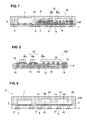
- FIG. 7 is a sectional view of a working example of another preferred embodiment of a component-embedded module according to the present invention.
- FIG. 8 is an enlarged sectional view of a sub-module of the component-embedded module shown in FIG. 7 .
- FIG. 9 is a sectional view of a working example another preferred embodiment of a component-embedded module according to the present invention.
- FIG. 10 is a drawing of the bottom surface of the sub-module of the component-embedded module shown in FIG. 9 .
- FIG. 11 is a plan view of a module substrate of the component-embedded module shown in FIG. 9 .
- FIGS. 1 to 3 show a first working example of a component-embedded module according to the present invention.
- FIG. 1 is an overall sectional view of the component-embedded module.
- FIG. 2 is a plan view of the component-embedded module excluding an insulating resin layer.
- FIG. 3 is an enlarged sectional view of a sub-module.
- the component-embedded module A includes a module substrate 1 preferably defined by an insulating substrate, such as a resin substrate, for example.
- a substrate having a single-layer structure is shown as the module substrate 1 .
- a multilayer substrate may also be used.
- multiple wiring electrodes 2 are provided on areas of the upper surface of the module substrate 1 , and are coupled to wiring electrodes 5 on the lower surface thereof through via conductors 3 .
- Some of the wiring electrodes 5 define terminal electrodes of the component-embedded module A.
- the via conductors 3 are also provided on an area on which a sub-module 10 (to be described later) is to be mounted, that is, on an area on which no wiring electrodes 2 are provided.
- the first circuit components 7 include a component 7 a having a height greater than that of a second circuit component 15 to be described later and components 7 b having heights less than those of the second circuit components 15 .
- the sub-module 10 shown in FIG. 3 is bonded and fixed to the area of the module substrate 1 on which no wiring electrodes 2 are provided.
- the sub-module 10 includes a sub-module substrate 11 that is preferably defined by a resin substrate, for example, and whose area is less than that of the module substrate 1 , second circuit components 15 mounted on the upper surface of the sub-module substrate 11 , and a resin layer 16 provided on the sub-module substrate 11 such that the resin layer 16 covers the second circuit components 15 . That is, the sub-module 10 according to this working example is preferably defined by a component-embedded substrate.
- the resin layer 16 is preferably made of a resin composition made of a thermosetting resin or a compound of a thermosetting resin and an inorganic filler, for example.
- Multiple wiring electrodes 12 are patterned on the upper surface of the sub-module substrate 11 .
- Multiple terminal electrodes 14 are independently provided on the lower surface thereof.
- the wiring electrodes 12 are coupled to the terminal electrodes 14 through via conductors 13 .
- the second circuit components 15 include an integrated circuit element 15 a, individual passive components 15 b, and other suitable components.
- the integrated circuit element 15 a is preferably flip-chip-mounted on the wiring electrodes 12 .
- the individual passive components 15 b are preferably mounted on other wiring electrodes 12 using precoating, soldering, a conductive adhesive, or other suitable bonding method, for example.
- the individual passive components 15 b as well as the integrated circuit element 15 a are mounted as the second circuit components 15 .
- only the integrated circuit element 15 a may be mounted.
- a shield electrode 17 is preferably provided on the upper surface of the resin layer 16 . The shield electrode 17 is coupled to the grounding wiring electrode 12 through a via conductor 18 and is further coupled to the grounding terminal electrodes 14 through via conductors 13 .
- An insulating resin layer 20 is provided on substantially the entire upper surface of the module substrate 1 .
- the first circuit components 7 and sub-module 10 are embedded in the insulating resin layer 20 .
- the insulating resin layer 20 is preferably, for example, a resin composition including a thermosetting resin or a compound of a thermosetting resin and an inorganic filler.
- the insulating resin layer 20 has a function of increasing the strength with which the module substrate 1 and sub-module 10 are fixed to each other and the strength with which the module substrate 1 and first circuit components 7 are fixed to each other.
- a shield layer 21 made of a copper foil or other suitable material, for example, is preferably provided on the upper surface of the resin layer 20 .
- the shield layer 21 is coupled to the grounding wiring electrode 2 on the module substrate 1 and the shield electrode 17 on the upper surface of the sub-module 10 through via conductors 22 .
- the lower surface of the sub-module 10 is preferably bonded and fixed to the area of the module substrate 1 on which no wiring electrodes 2 are provided.
- the via conductors 3 provided on the module substrate 1 are preferably directly coupled to the terminal electrodes 14 provided on the lower surface of the sub-module 10 . That is, no wiring electrodes for mounting are provided on the upper surface of the module substrate 1 opposed to the sub-module 10 , nor is a bonding material for mounting the sub-module 10 provided thereon. This makes it possible to fix the sub-module 10 onto the module substrate 1 such that the sub-module 10 is brought into close contact with the module substrate 1 . This makes it possible to reduce the thickness of the component-embedded module A.
- an identical material or materials having thermal expansion coefficients close to each other may preferably be used, for example.
- an identical material or materials having thermal expansion coefficients close to each other may preferably be used, for example.
- a material having a thermal expansion coefficient close to that of the integrated circuit element 15 a may preferably be used, for example.
- a material having a thermal expansion coefficient that is in between that of the sub-module 10 and that of a motherboard, on which the component-embedded module A is to be mounted may preferably be used, for example.
- the difference between the thermal expansion coefficient of the integrated circuit element 15 a and that of the motherboard can be reduced using the module substrate 1 and sub-module 10 .
- a problem such as peeling off of an electrode (terminal) due to variations in temperature can be eliminated.
- a material having a middle thermal expansion coefficient may preferably be used, for example.
- the first circuit components 7 include the component 7 a having a height greater than those of the second circuit components 15 , the heights of the first circuit components 7 and that of the sub-module 10 are averaged. Thus, the overall height of the component-embedded module A can be reduced. While an example in which the thicknesses of the first circuit components 7 are slightly greater than that of the sub-module 10 is shown in FIG. 1 , the thickness of the sub-module 10 may be greater than those of the first circuit components 7 or the thicknesses of the first circuit components 7 and that of the sub-module 10 may be equal to each other. Also, the shield layer 21 on the upper surface of the insulating resin layer 20 and the via conductors 22 may be omitted.
- the sub-module 10 is required to have a wiring accuracy greater than that of the module substrate 1 . That is, the sub-module 10 must be a substrate manufactured under a more stringent design than that for the module substrate 1 . For this reason, the unit cost per unit area of the sub-module 10 is greater than that of the module substrate 1 . However, the cost can be made less than that when the entire module substrate 1 is made of a substrate having a high wiring accuracy, since the sub-module 10 is less than the module substrate 1 .
- the integrated circuit element 15 a Since the integrated circuit element 15 a is flip-chip-mounted on the sub-module substrate 11 , it is difficult to check the mounting state (coupling state) visually. For this reason, it is necessary to electrically inspect the mounting state. While it is possible to perform an inspection after the component-embedded module A is completed, the entire module A must be discarded if a failure is discovered.
- the integrated circuit element 15 a is mounted on the sub-module substrate 11 . Therefore, it is possible to inspect the coupling state of the integrated circuit element 15 a in the stage of the sub-module 10 , before forming the resin layer 16 . Specifically, it is sufficient to measure electrical characteristics using the terminal electrodes 14 of the sub-module 10 . If a failure is found in this stage, it is possible to demount the integrated circuit element 15 a from the sub-module substrate 11 and remount an integrated circuit element 15 a. This significantly increases the yield.
- FIGS. 4A-4H an example of a method for manufacturing the component-embedded module A having the above-mentioned configuration will be described with reference to FIGS. 4A-4H . While a method for manufacturing the component-embedded module A placed in a child-substrate-state will be described hereafter, in practice, the component-embedded modules A are manufactured in a combined-substrate-state where multiple child substrates are combined and then the combined substrate is divided into child substrates.
- the sub-module 10 and first circuit components 7 and a support plate 30 are prepared.
- the wiring electrodes 2 are preferably formed on some areas of the upper surface of the support plate 30 , for example, by patterning a metal foil.
- multiple resist patterns 31 are formed such that the resist patterns surround an area S on which no wiring electrodes 2 are formed.
- the sub-module 10 is mounted on the area S.
- a bonding sheet 32 is bonded to the lower surface of the sub-module 10 , that is, the surface on which the terminal electrodes 14 are formed.
- the bonding sheet 32 is preferably, for example, a thin, thermosetting resin sheet having a thickness of about 50 ⁇ m.
- the bonding sheet 32 it is preferable to use a material identical or substantially identical to that of the resin layer 16 of the sub-module 10 or that of the insulating resin layer 20 of the module substrate 1 . This makes it possible to make all the materials covering the sub-module identical to one another. This is intended to prevent unevenness in thermal expansion coefficient and to stabilize the structure and characteristics.
- the bonding sheet 32 is not required to be a previously shaped sheet and may be, for example, a yet-to-be-cured bonding layer that is applied to the upper surface of the support plate 30 or the lower surface of the sub-module 10 by printing or other suitable method.
- FIG. 4B shows a state in which the sub-module 10 is bonded to the area S of the support plate 30 using the bonding sheet 32 and the first circuit components 7 are mounted on the wiring electrodes 2 near the sub-module 10 .
- the perimeter of the sub-module 10 is positioned using the resist patterns 31 .
- the resist patterns 31 are formed in accordance with the external shape of the sub-module 10 .
- a method for mounting the first circuit components 7 may or the like be precoating mounting, reflow soldering, flip-chip mounting using bumps, or mounting using a conductive adhesive, for example.
- the thickness of the bonding sheet 32 is preferably reduced to, e.g., about 20 ⁇ m to about 30 ⁇ m. This also allows the bonding sheet 32 to extend to the sides of the sub-module 10 . Thus, the strength with which the sub-module 10 is fixed is increased. Also, the terminal electrodes 14 are formed on the lower surface of the sub-module 10 and thus small bumps and dips occur.
- the bonding sheet 32 softens due to heat crimping, it is possible to reliably bridge gaps created between the sub-module 10 and support plate 30 by the bumps and dips. While the sub-module 10 may be misaligned due to the softening, such misalignment is prevented by positioning the perimeter of the sub-module 10 using the heat-resistant resist patterns 31 . After the bonding, the bonding sheet 32 is cured.
- FIG. 4C shows a state in which the insulating resin layer 20 is formed on substantially the entire upper surface of the support plate 30 such that the insulating resin layer 20 covers the sub-module 10 and first circuit components 7 and the shield layer 21 is formed on the upper surface of the insulating resin layer 20 .
- a method for forming the insulating resin layer 20 and shield layer 21 may preferably be, for example, a method of disposing a copper foil, which is to become the shield layer 21 , on the upper surface of the insulating resin layer 20 placed in a B-stage (semi-cured) state, crimping the insulating resin layer 20 onto the support plate 30 , and then curing the insulating resin layer 20 , or a method of molding an insulating resin on the support plate 30 , curing the insulating resin, and then forming the shield layer 21 on the upper surface of the insulating resin layer 20 by electroless plating, for example. Any other methods may be used to form the insulating resin layer 20 and shield layer 21 . While an example in which the insulating resin layer 20 covers substantially the entire sub-module 10 and first circuit components 7 is shown here, a portion of the sub-module 10 or a portion of the first circuit components 7 may be exposed from the insulating resin layer 20 .
- FIG. 4D shows a state in which, after the insulating resin layer 20 is cured, a via hole extending to the ground electrode 2 on the upper surface of the support plate 30 and via holes extending to the shield electrode 17 on the upper surface of the sub-module 10 are formed through the insulating resin layer 20 and are then filled with conductors, such as conductive pastes, for example, then the conductors are cured, and thus via conductors 22 are formed and coupled to the shield layer 21 .
- the via holes can be formed using a known method, such as a method of making openings on areas, on which via holes need to be formed, of the copper foil on the upper surface of the insulating resin layer 20 and applying lasers so that the lasers pass through the openings, for example.
- the via conductors 22 are not limited to via conductors formed by filling the via holes with conductors and may be through hole conductors formed by forming electrode films on the inner surfaces of the via holes by electroless plating, for example.
- FIG. 4E shows a state in which after the insulating resin layer 20 is cured, the support plate 30 is peeled off.
- the wiring electrodes 2 , the insulating resin layer 20 , and the lower surface (cured bonding sheet 32 ) of sub-module 10 are exposed on the lower surface from which the support plate 30 has been peeled off.
- FIG. 4F shows a state in which the thin module substrate 1 is bonded to the lower surface from which the support plate 30 has been peeled off. Since the module substrate 1 is in a semi-cured state (B stage) at the time of bonding, the module substrate 1 , and the wiring electrodes 2 , insulating resin layer 20 , and sub-module 10 are preferably brought into close contact with each other by crimping the module substrate 1 . In this state, the module substrate 1 is cured.
- FIG. 4G shows a state in which via holes 3 a are formed through the cured module substrate 1 from the lower surface thereof using lasers. At that time, the via holes 3 a are formed to a depth extending to the wiring electrodes 2 , and are formed to a depth extending to the terminal electrodes 14 through the bonding sheet 32 bonded to the lower surface of the sub-module 10 .
- FIG. 4H shows a state in which via conductors 3 or through hole conductors are formed by embedding conductors in the via holes 3 a or performing a plating process on the inner surfaces of the via holes 3 a.
- the wiring electrodes 5 are patterned on the lower surface of the module substrate 1 such that the wiring electrodes 5 cover the via conductors 3 .
- the wiring electrodes 5 and wiring electrodes 2 are coupled to each other, and the wiring electrodes 5 and terminal electrodes 14 are coupled to each other.
- the component-embedded module A is completed.
- FIGS. 6A-6G show another method for manufacturing the component-embedded module A.
- the same elements as those in FIGS. 4A to 4H are assigned the same reference numerals and descriptions there will not be repeated.
- the cured module substrate 1 is initially prepared and the wiring electrodes 2 are formed on the upper surface of the module substrate 1 .
- the resist patterns 31 are formed on the area S on which no wiring electrodes 2 are formed such that the resist patterns 31 surround the area S.
- the module substrate 1 is a thin-layer substrate, the strength thereof is relatively low and warpage or distortion easily occurs. For this reason, it is preferable to support the lower surface of the module substrate 1 with a reinforcing plate 35 having high flatness and high strength.
- the module substrate 1 may preferably be bonded to the reinforcing plate 35 using a heatproof tape, a sheet whose adhesiveness varies with the temperature, or other suitable bonding agent, for example. Further, the module substrate 1 may be supported by using a plate with air vents as the reinforcing plate 35 and evacuating the air vents.
- the first circuit components 7 are mounted on the wiring electrodes 2 and the sub-module 10 is bonded and fixed to the area S using the bonding sheet 32 .
- the bonding sheet 32 is softened. This makes it possible to bridge the gaps between the module substrate 1 and sub-module 10 and to fix the sub-module 10 .
- FIG. 6C shows a state in which the insulating resin layer 20 is crimped or molded on the module substrate 1 and the shield layer 21 is formed on the upper surface of the insulating resin layer 20 .
- the first circuit components 7 and sub-module 10 are embedded in the insulating resin layer 20 .
- FIG. 6D shows a state in which after the insulating resin layer 20 is cured, a via hole extending to the ground electrode 2 on the upper surface of the module substrate 1 and via holes extending to the shield electrode 17 on the upper surface of the sub-module 10 are formed through the insulating resin layer 20 and then filled with conductors and the conductors are cured, and thus via conductors 22 are formed and coupled to the shield layer 21 .
- FIG. 6E shows a state in which the reinforcing plate 35 supporting the lower surface of the module substrate 1 is eliminated. If the module substrate 1 and reinforcing plate 35 are bonded together using a heatproof tape, the tape is peeled off. If a sheet, whose adhesiveness varies with the temperature, is used, the reinforcing plate 35 is eliminated by lowering the temperature to a temperature at which the adhesiveness decreases.
- FIG. 6F shows a state in which the via holes 3 a are formed through the module substrate 1 from the lower surface thereof using lasers. At that time, the via holes 3 a are formed to a depth extending to the wiring electrodes 2 and the terminal electrodes 14 on the lower surface of the sub-module 10 .
- FIG. 6G shows a state in which the via conductors 3 or through hole conductors are formed by embedding conductors in the via holes 3 a or performing a plating process on the inner surfaces of the via holes 3 a and the wiring electrodes 5 are patterned on the lower surface of the module substrate 1 .
- the wiring electrodes 5 and wiring electrodes 2 are coupled to each other, and the wiring electrodes 5 and terminal electrodes 14 are coupled to each other.
- the component-embedded module A is completed.
- the cured module substrate 1 is used. Therefore, the number of curing process steps can be reduced by one as compared to that in the manufacturing method shown in FIGS. 4A to 4H . Also, while the support plate 30 is typically thrown away after one use in FIGS. 4A to 4H , the module substrate 1 also functions as a support plate and therefore no base material is required in FIGS. 6A to 6G .
- the module substrate 1 having no wiring electrodes 5 on the lower surface thereof is preferably used. However, a module substrate 1 having the wiring electrodes 5 patterned on the lower surface thereof in advance may be used.
- the module substrate 1 is preferably bonded to the reinforcing plate 35 so that deformation of the module substrate 1 is restrained.
- any suitable support method may be used as long as the support method is a method by which the reinforcing plate 35 can be easily eliminated in a later step and the module substrate 1 can withstand the temperature or pressure when forming the insulating resin layer 20 .
- FIGS. 7 and 8 show a second working example of a component-embedded module. Elements corresponding to those in the first working example are assigned the same reference numerals and descriptions thereof will not be repeated.
- a sub-module substrate 11 A having a multilayer structure as shown in FIG. 8 is used as a sub-module 10 A.
- inner-layer electrodes 19 By forming inner-layer electrodes 19 inside the sub-module substrate 11 A, capacitances or resistances can be formed inside the sub-module substrate 11 A.
- a multifunctional sub-module 10 A can be provided.
- a resin composition, a ceramic material, or other suitable material can preferably be used, for example.
- the integrated circuit element 15 a and individual passive components 15 b included in the second circuit components 15 are mounted on the upper surface of the sub-module substrate 11 A. No resin layer 16 (see FIG. 3 ) is provided thereon.
- the second circuit components 15 are embedded in the insulating resin layer 20 .
- the sub-module 10 A does not include the resin layer 16 . Therefore, the thickness of the sub-module 10 A can be reduced accordingly. In particular, if the heights of the first circuit components 7 are relatively low, the heights of the first circuit components 7 and that of the sub-module 10 A can be matched. Thus, the thickness of the module B can be further reduced.
- FIGS. 9 to 11 show a third working example of a component-embedded module. This working example is intended to show another method for fixing a sub-module to a module substrate. Elements corresponding to those in the first working example are assigned the same reference numerals and descriptions thereof will not be repeated.
- the terminal electrodes 14 are provided on the lower surface of a sub-module 10 B in a matrix as shown in FIG. 10 and an appropriate number (here, four) of dummy electrodes 40 are preferably provided in gaps between the terminal electrodes 14 .
- the dummy electrodes 40 are lands that are not associated with electrical coupling between the sub-module 10 B and module substrate 1 , and are provided independently of the terminal electrodes 14 .
- the size, positions and the number of the dummy electrodes 40 are not particularly limited as long as they have no negative influence on the mountability or the electrical characteristics of the sub-module. As shown in FIG.
- lands 41 for fixing a sub-module are provided on the module substrate 1 corresponding to the dummy electrodes 40 .
- the lands 41 are lands that are not coupled to the via conductors 3 to be provided in a later step.
- the lands 41 for fixing a sub-module are subjected to Sn plating, as with the land portions of the wiring electrodes 2 for mounting the first circuit components 7 ( 7 a, 7 b ).
- terminal electrodes 14 of the sub-module 10 B do not always need to be disposed in a matrix as shown in FIG. 10 and may be disposed peripherally (peripheral disposition) or randomly.
- the sub-module 10 B is fixed to the module substrate 1 using the dummy electrodes 40 and then the insulating resin layer 20 is provided such that the insulating resin layer 20 covers the sub-module 10 B and first circuit components 7 .
- a narrow space is provided between the sub-module 10 B and module substrate 1 unlike in FIGS. 6A to 6G , a resin is fluidized during formation of the insulating resin layer 20 such that the narrow space is also filled with the resin.
- the same steps as those in FIGS. 6D to 6 G are performed.
- the via holes are formed through the module substrate 1 and bonding sheet 32 such that the via holes extend to the terminal electrodes of the sub-module.
- the bonding sheet 32 does not exist, and therefore, via holes are preferably formed such that the via holes extend through the insulating resin layer 20 located below the sub-module 10 B and to the terminal electrodes 14 of the sub-module 10 B. Therefore, the via conductors 3 are coupled to terminal electrodes 14 through the insulating resin layer 20 .
- the sub-module 10 B can preferably be fixed to the module substrate 1 using the same Sn precoating construction method as that used to fix the first circuit components 7 . That is, the first circuit components 7 and sub-module 10 B can be collectively mounted. Therefore, the number of steps can be reduced. Also, by applying Sn precoating, the amount of solder is significantly reduced as compared to that in a case in which the sub-module is mounted on the module substrate by soldering. Also, the anti-solder flash capability is enhanced.
- a thickness of about 80 ⁇ m to about 100 ⁇ m, for example, is preferred since metal masks are formed on the lands 41 for fixing a sub-module and then a solder paste is formed.
- mounting can be performed by only performing Sn plating on the lands 41 for fixing a sub-module by a thickness of about 1 ⁇ m, for example. Therefore, the height of the entire component-embedded module can be reduced.
- the present invention is not limited to the above-mentioned working examples of preferred embodiments. While examples in which one sub-module is mounted on a module substrate are shown in the above-mentioned working examples, multiple sub-modules may be mounted on a module substrate. In this case, the multiple sub-modules may preferably be mounted at intervals and the first circuit components may be mounted in the intermediate positions between the sub-modules. In this case, the sub-modules are disposed on both sides of the first circuit components 7 . Therefore, the strength of the module substrate against warpage and the strength thereof against shock are improved. If multiple sub-modules are mounted, it is not necessary to mount an integrated circuit element on each of the sub-modules or embed an integrated circuit element in each sub-module, and only passive components similar to the first circuit components may be mounted on each sub-module.
- the sub-module a sub-module formed by mounting the second circuit components on a sub-module substrate having a single-layer structure or a multilayer structure, or a sub-module formed by mounting the second circuit components on a sub-module substrate and then forming a resin layer on the second circuit components is used.
- the sub-module may be formed using only a resin layer without including a sub-module substrate.
- the sub-module manufacturing methods may be substantially the same as those shown in FIGS. 4A to 4E .
- a sub-module substrate of a sub-module may be formed using a component-embedded substrate and the second circuit components may be mounted on the upper surface of the component-embedded substrate.
Applications Claiming Priority (3)
| Application Number | Priority Date | Filing Date | Title |
|---|---|---|---|
| JP2007121412 | 2007-05-02 | ||
| JP2007-121412 | 2007-05-02 | ||
| PCT/JP2008/057155 WO2008136251A1 (ja) | 2007-05-02 | 2008-04-11 | 部品内蔵モジュール及びその製造方法 |
Related Parent Applications (1)
| Application Number | Title | Priority Date | Filing Date |
|---|---|---|---|
| PCT/JP2008/057155 Continuation WO2008136251A1 (ja) | 2007-05-02 | 2008-04-11 | 部品内蔵モジュール及びその製造方法 |
Publications (2)
| Publication Number | Publication Date |
|---|---|
| US20100027225A1 US20100027225A1 (en) | 2010-02-04 |
| US8072769B2 true US8072769B2 (en) | 2011-12-06 |
Family
ID=39943368
Family Applications (1)
| Application Number | Title | Priority Date | Filing Date |
|---|---|---|---|
| US12/579,617 Active 2028-10-08 US8072769B2 (en) | 2007-05-02 | 2009-10-15 | Component-embedded module and manufacturing method thereof |
Country Status (5)
| Country | Link |
|---|---|
| US (1) | US8072769B2 (ja) |
| EP (1) | EP2141972B1 (ja) |
| JP (1) | JP4424449B2 (ja) |
| CN (1) | CN101663926B (ja) |
| WO (1) | WO2008136251A1 (ja) |
Cited By (7)
| Publication number | Priority date | Publication date | Assignee | Title |
|---|---|---|---|---|
| US20130223041A1 (en) * | 2012-02-23 | 2013-08-29 | Apple Inc. | Low profile, space efficient circuit shields |
| US9107290B1 (en) | 2014-03-05 | 2015-08-11 | Delta Electronics Int'l (Singapore) Pte Ltd | Package structure and stacked package module with the same |
| US9198284B2 (en) | 2010-08-06 | 2015-11-24 | Panasonic Intellectual Property Management Co., Ltd. | Circuit board and method for manufacturing same |
| US9351410B2 (en) * | 2014-03-07 | 2016-05-24 | Fujikura Ltd. | Electronic component built-in multi-layer wiring board and method of manufacturing the same |
| US9425131B2 (en) | 2014-03-05 | 2016-08-23 | Delta Electronics Int'l (Singapore) Pte Ltd | Package structure |
| US9913380B2 (en) | 2016-05-31 | 2018-03-06 | Delta Electronics Int'l (Singapore) Pte Ltd | Embedded package structure |
| US20180093338A1 (en) * | 2014-12-18 | 2018-04-05 | Zkw Group Gmbh | Method for void reduction in solder joints |
Families Citing this family (50)
| Publication number | Priority date | Publication date | Assignee | Title |
|---|---|---|---|---|
| US8106496B2 (en) * | 2007-06-04 | 2012-01-31 | Stats Chippac, Inc. | Semiconductor packaging system with stacking and method of manufacturing thereof |
| WO2010109985A1 (ja) * | 2009-03-25 | 2010-09-30 | 株式会社村田製作所 | 電子部品の製造方法 |
| JP5418395B2 (ja) * | 2010-05-06 | 2014-02-19 | 大日本印刷株式会社 | 樹脂製パッケージの製造方法、部品内蔵樹脂モジュールの製造方法、樹脂製パッケージ配列シート、部品内蔵樹脂モジュール配列シート |
| KR101070814B1 (ko) * | 2010-06-03 | 2011-10-06 | 삼성전기주식회사 | 반도체패키지 및 그 제조방법 |
| KR101070799B1 (ko) * | 2010-06-03 | 2011-10-06 | 삼성전기주식회사 | 반도체패키지 및 그 제조방법 |
| TWI472007B (zh) * | 2010-12-28 | 2015-02-01 | Ind Tech Res Inst | 內埋式電子元件之封裝結構 |
| JP5892388B2 (ja) * | 2011-01-12 | 2016-03-23 | 株式会社村田製作所 | 樹脂封止型モジュール |
| JP5672091B2 (ja) * | 2011-03-17 | 2015-02-18 | 株式会社村田製作所 | 多層基板 |
| US8674235B2 (en) | 2011-06-06 | 2014-03-18 | Intel Corporation | Microelectronic substrate for alternate package functionality |
| US9129908B2 (en) | 2011-11-15 | 2015-09-08 | Cisco Technology, Inc. | Manufacturing a semiconductor package including an embedded circuit component within a support structure of the package |
| JP6157821B2 (ja) * | 2012-09-26 | 2017-07-05 | イビデン株式会社 | 配線板及びその製造方法 |
| JP6082233B2 (ja) * | 2012-10-31 | 2017-02-15 | イビデン株式会社 | 配線板及びその製造方法 |
| JP5285819B1 (ja) * | 2012-11-07 | 2013-09-11 | 太陽誘電株式会社 | 電子回路モジュール |
| CN203151864U (zh) | 2013-03-05 | 2013-08-21 | 奥特斯(中国)有限公司 | 印制电路板 |
| US8877554B2 (en) | 2013-03-15 | 2014-11-04 | Taiwan Semiconductor Manufacturing Company, Ltd. | Packaged semiconductor devices, methods of packaging semiconductor devices, and PoP devices |
| CN105027692B (zh) * | 2013-05-17 | 2018-01-30 | 株式会社村田制作所 | 元器件内置多层基板的制造方法以及元器件内置多层基板 |
| CN107658275A (zh) * | 2013-05-31 | 2018-02-02 | 日月光半导体制造股份有限公司 | 堆叠式多封装模块及其制造方法 |
| JP2015023194A (ja) * | 2013-07-19 | 2015-02-02 | 株式会社東芝 | 半導体装置 |
| JP5583828B1 (ja) * | 2013-08-05 | 2014-09-03 | 株式会社フジクラ | 電子部品内蔵多層配線基板及びその製造方法 |
| JP6206092B2 (ja) * | 2013-10-29 | 2017-10-04 | 富士通株式会社 | 電子部品およびその製造方法 |
| CN104640350B (zh) * | 2013-11-11 | 2018-04-20 | 日月光半导体制造股份有限公司 | 电路板模块 |
| TWI491329B (zh) * | 2013-11-11 | 2015-07-01 | Advanced Semiconductor Eng | 電路板模組 |
| JP2015176984A (ja) * | 2014-03-14 | 2015-10-05 | 株式会社東芝 | プリント配線板 |
| US9299736B2 (en) | 2014-03-28 | 2016-03-29 | Taiwan Semiconductor Manufacturing Company, Ltd. | Hybrid bonding with uniform pattern density |
| US9829915B2 (en) * | 2014-06-18 | 2017-11-28 | Intel Corporation | Modular printed circuit board |
| JP6380548B2 (ja) * | 2014-10-16 | 2018-08-29 | 株式会社村田製作所 | 複合デバイス |
| KR102117477B1 (ko) | 2015-04-23 | 2020-06-01 | 삼성전기주식회사 | 반도체 패키지 및 반도체 패키지의 제조방법 |
| KR102486558B1 (ko) * | 2015-06-24 | 2023-01-10 | 삼성전자주식회사 | 회로 기판 및 이를 구비한 반도체 패키지 |
| US9673173B1 (en) * | 2015-07-24 | 2017-06-06 | Altera Corporation | Integrated circuit package with embedded passive structures |
| CN106409793B (zh) * | 2015-07-29 | 2019-11-26 | 乾坤科技股份有限公司 | 具有电磁屏蔽结构的电子模组及其制造方法 |
| TWI621378B (zh) * | 2015-07-29 | 2018-04-11 | 乾坤科技股份有限公司 | 具有電磁屏蔽結構的電子模組及其製造方法 |
| JP2017123459A (ja) | 2016-01-08 | 2017-07-13 | サムソン エレクトロ−メカニックス カンパニーリミテッド. | プリント回路基板 |
| KR101787882B1 (ko) * | 2016-03-29 | 2017-10-19 | 앰코 테크놀로지 코리아 주식회사 | 반도체 패키지 및 그 제조 방법 |
| JP6621708B2 (ja) * | 2016-05-26 | 2019-12-18 | 新光電気工業株式会社 | 半導体装置、半導体装置の製造方法 |
| US10306332B2 (en) * | 2016-06-14 | 2019-05-28 | DISH Technologies L.L.C. | Use of audio signals to provide interactive content to end users via smart devices |
| WO2018003391A1 (ja) | 2016-06-29 | 2018-01-04 | 株式会社村田製作所 | 部品内蔵基板及びその製造方法、並びに高周波モジュール |
| US10616184B2 (en) | 2016-06-30 | 2020-04-07 | Intel Corporation | Wireless display streaming of protected content |
| JP6669034B2 (ja) * | 2016-10-14 | 2020-03-18 | オムロン株式会社 | 樹脂構造体、電子機器、および樹脂構造体の製造方法 |
| DE102018111989A1 (de) * | 2018-05-18 | 2019-11-21 | Rogers Germany Gmbh | Elektronikmodul und Verfahren zur Herstellung desselben |
| JP2020061406A (ja) * | 2018-10-05 | 2020-04-16 | 株式会社村田製作所 | 半導体装置 |
| JPWO2020149104A1 (ja) * | 2019-01-15 | 2021-11-25 | 株式会社村田製作所 | 電子回路モジュール、検査方法、及び通信装置 |
| WO2021019684A1 (ja) * | 2019-07-30 | 2021-02-04 | 株式会社Fuji | スタック部品の製造方法 |
| WO2021131774A1 (ja) * | 2019-12-27 | 2021-07-01 | 株式会社村田製作所 | モジュール |
| CN114868245A (zh) * | 2019-12-27 | 2022-08-05 | 株式会社村田制作所 | 模块 |
| WO2022065395A1 (ja) * | 2020-09-25 | 2022-03-31 | 株式会社村田製作所 | 電子部品モジュール、および、電子部品モジュールの製造方法 |
| KR20220076894A (ko) * | 2020-12-01 | 2022-06-08 | 삼성전자주식회사 | 지지 부재를 갖는 반도체 패키지 |
| US11469162B2 (en) * | 2020-12-07 | 2022-10-11 | Richtek Technology Corporation | Plurality of vertical heat conduction elements attached to metal film |
| JP2022096837A (ja) * | 2020-12-18 | 2022-06-30 | 株式会社村田製作所 | 半導体装置、及び半導体モジュール |
| WO2023135911A1 (ja) * | 2022-01-17 | 2023-07-20 | 株式会社村田製作所 | 高周波モジュール |
| WO2024029313A1 (ja) * | 2022-08-01 | 2024-02-08 | 株式会社村田製作所 | モジュール |
Citations (22)
| Publication number | Priority date | Publication date | Assignee | Title |
|---|---|---|---|---|
| JPH05136558A (ja) | 1991-11-11 | 1993-06-01 | Fujitsu Ltd | プリント板ユニツトの実装方法 |
| JPH08191128A (ja) | 1995-01-09 | 1996-07-23 | Hitachi Ltd | 電子装置 |
| JPH1140918A (ja) | 1997-07-22 | 1999-02-12 | Taiyo Yuden Co Ltd | セラミックス素子、部品実装基板及び配線基板 |
| US5926379A (en) | 1995-12-07 | 1999-07-20 | Sagem Sa | Electronic card assembly by means of solder connections |
| JP2001177043A (ja) | 1999-12-15 | 2001-06-29 | Matsushita Electric Ind Co Ltd | 電子モジュール |
| JP2002110717A (ja) | 2000-10-02 | 2002-04-12 | Sanyo Electric Co Ltd | 回路装置の製造方法 |
| US20020052062A1 (en) | 2000-10-02 | 2002-05-02 | Noriaki Sakamoto | Method of manufacturing circuit device |
| EP1225629A2 (en) | 2001-01-19 | 2002-07-24 | Matsushita Electric Industrial Co., Ltd. | Component built-in module and method of manufacturing the same |
| JP2002290051A (ja) | 2001-01-19 | 2002-10-04 | Matsushita Electric Ind Co Ltd | 部品内蔵モジュールとその製造方法 |
| JP2002344146A (ja) | 2001-05-15 | 2002-11-29 | Tdk Corp | 高周波モジュールとその製造方法 |
| JP2003188538A (ja) | 2001-12-18 | 2003-07-04 | Murata Mfg Co Ltd | 多層基板、および多層モジュール |
| US20040105243A1 (en) | 2002-10-03 | 2004-06-03 | Kuang-Hua Lee | Electronic device having a plurality of metallic balls for transmitting signals between two circuit boards |
| JP2005251904A (ja) | 2004-03-03 | 2005-09-15 | Denso Corp | 基板表面実装部品、基板回路、基板、ハンダ接続方法、及び基板回路の製造方法 |
| US20060001166A1 (en) | 2004-06-30 | 2006-01-05 | Yusuke Igarashi | Circuit device and manufacturing method thereof |
| JP2006032402A (ja) | 2004-07-12 | 2006-02-02 | Alps Electric Co Ltd | 電子部品の実装構造および実装方法 |
| JP2006173167A (ja) | 2004-12-13 | 2006-06-29 | Murata Mfg Co Ltd | ランド構造,インダクタ部品取付構造及び無線通信機の電源回路 |
| US20070030628A1 (en) | 2005-08-05 | 2007-02-08 | Ngk Spark Plug Co., Ltd. | Capacitor for incorporation in wiring board, wiring board, method of manufacturing wiring board, and ceramic chip for embedment |
| JP2007067369A (ja) | 2005-08-05 | 2007-03-15 | Ngk Spark Plug Co Ltd | 配線基板及びその製造方法、埋め込み用セラミックチップ |
| WO2007034629A1 (ja) | 2005-09-20 | 2007-03-29 | Murata Manufacturing Co., Ltd. | 部品内蔵モジュールの製造方法および部品内蔵モジュール |
| US20070081312A1 (en) | 2004-07-30 | 2007-04-12 | Murata Manufacturing Co., Ltd. | Composite electronic component and method of manufacturing the same |
| WO2007072616A1 (ja) | 2005-12-22 | 2007-06-28 | Murata Manufacturing Co., Ltd. | 部品内蔵モジュールおよびその製造方法 |
| US7315455B2 (en) * | 2002-08-29 | 2008-01-01 | Fujitsu Media Devices Ltd. | Surface-mounted electronic component module and method for manufacturing the same |
-
2008
- 2008-04-11 EP EP08740252.5A patent/EP2141972B1/en active Active
- 2008-04-11 WO PCT/JP2008/057155 patent/WO2008136251A1/ja active Application Filing
- 2008-04-11 JP JP2009512911A patent/JP4424449B2/ja active Active
- 2008-04-11 CN CN2008800121865A patent/CN101663926B/zh active Active
-
2009
- 2009-10-15 US US12/579,617 patent/US8072769B2/en active Active
Patent Citations (26)
| Publication number | Priority date | Publication date | Assignee | Title |
|---|---|---|---|---|
| JPH05136558A (ja) | 1991-11-11 | 1993-06-01 | Fujitsu Ltd | プリント板ユニツトの実装方法 |
| JPH08191128A (ja) | 1995-01-09 | 1996-07-23 | Hitachi Ltd | 電子装置 |
| US5926379A (en) | 1995-12-07 | 1999-07-20 | Sagem Sa | Electronic card assembly by means of solder connections |
| JPH1140918A (ja) | 1997-07-22 | 1999-02-12 | Taiyo Yuden Co Ltd | セラミックス素子、部品実装基板及び配線基板 |
| JP2001177043A (ja) | 1999-12-15 | 2001-06-29 | Matsushita Electric Ind Co Ltd | 電子モジュール |
| US20020052062A1 (en) | 2000-10-02 | 2002-05-02 | Noriaki Sakamoto | Method of manufacturing circuit device |
| JP2002110717A (ja) | 2000-10-02 | 2002-04-12 | Sanyo Electric Co Ltd | 回路装置の製造方法 |
| EP1225629A2 (en) | 2001-01-19 | 2002-07-24 | Matsushita Electric Industrial Co., Ltd. | Component built-in module and method of manufacturing the same |
| JP2002290051A (ja) | 2001-01-19 | 2002-10-04 | Matsushita Electric Ind Co Ltd | 部品内蔵モジュールとその製造方法 |
| JP2002344146A (ja) | 2001-05-15 | 2002-11-29 | Tdk Corp | 高周波モジュールとその製造方法 |
| JP2003188538A (ja) | 2001-12-18 | 2003-07-04 | Murata Mfg Co Ltd | 多層基板、および多層モジュール |
| US7315455B2 (en) * | 2002-08-29 | 2008-01-01 | Fujitsu Media Devices Ltd. | Surface-mounted electronic component module and method for manufacturing the same |
| US20040105243A1 (en) | 2002-10-03 | 2004-06-03 | Kuang-Hua Lee | Electronic device having a plurality of metallic balls for transmitting signals between two circuit boards |
| JP2005251904A (ja) | 2004-03-03 | 2005-09-15 | Denso Corp | 基板表面実装部品、基板回路、基板、ハンダ接続方法、及び基板回路の製造方法 |
| JP2006019361A (ja) | 2004-06-30 | 2006-01-19 | Sanyo Electric Co Ltd | 回路装置およびその製造方法 |
| US20060001166A1 (en) | 2004-06-30 | 2006-01-05 | Yusuke Igarashi | Circuit device and manufacturing method thereof |
| JP2006032402A (ja) | 2004-07-12 | 2006-02-02 | Alps Electric Co Ltd | 電子部品の実装構造および実装方法 |
| US20070081312A1 (en) | 2004-07-30 | 2007-04-12 | Murata Manufacturing Co., Ltd. | Composite electronic component and method of manufacturing the same |
| JP2006173167A (ja) | 2004-12-13 | 2006-06-29 | Murata Mfg Co Ltd | ランド構造,インダクタ部品取付構造及び無線通信機の電源回路 |
| US20070030628A1 (en) | 2005-08-05 | 2007-02-08 | Ngk Spark Plug Co., Ltd. | Capacitor for incorporation in wiring board, wiring board, method of manufacturing wiring board, and ceramic chip for embedment |
| JP2007067369A (ja) | 2005-08-05 | 2007-03-15 | Ngk Spark Plug Co Ltd | 配線基板及びその製造方法、埋め込み用セラミックチップ |
| WO2007034629A1 (ja) | 2005-09-20 | 2007-03-29 | Murata Manufacturing Co., Ltd. | 部品内蔵モジュールの製造方法および部品内蔵モジュール |
| US20080149381A1 (en) | 2005-09-20 | 2008-06-26 | Murata Manufacturing Co., Ltd. | Method for manufacturing component incorporating module and component incorporating module |
| US7885081B2 (en) * | 2005-09-20 | 2011-02-08 | Murata Manufacturing Co., Ltd. | Component incorporating module |
| WO2007072616A1 (ja) | 2005-12-22 | 2007-06-28 | Murata Manufacturing Co., Ltd. | 部品内蔵モジュールおよびその製造方法 |
| US20070170582A1 (en) | 2005-12-22 | 2007-07-26 | Murata Manufacturing Co., Ltd. | Component-containing module and method for producing the same |
Non-Patent Citations (4)
| Title |
|---|
| Official Communication issued in corresponding Chinese Patent Application No. 200880012186.5, mailed on Sep. 13, 2010. |
| Official Communication issued in corresponding European Patent Application No. 08740252.5, mailed on Dec. 6, 2010. |
| Official Communication issued in corresponding Japanese Patent Application No. 2009-512911, drafted on Sep. 3, 2009. |
| Official Communication issued in International Patent Application No. PCT/JP2008/057155, mailed on May 27, 2008. |
Cited By (9)
| Publication number | Priority date | Publication date | Assignee | Title |
|---|---|---|---|---|
| US9198284B2 (en) | 2010-08-06 | 2015-11-24 | Panasonic Intellectual Property Management Co., Ltd. | Circuit board and method for manufacturing same |
| US20130223041A1 (en) * | 2012-02-23 | 2013-08-29 | Apple Inc. | Low profile, space efficient circuit shields |
| US9030841B2 (en) * | 2012-02-23 | 2015-05-12 | Apple Inc. | Low profile, space efficient circuit shields |
| US9107290B1 (en) | 2014-03-05 | 2015-08-11 | Delta Electronics Int'l (Singapore) Pte Ltd | Package structure and stacked package module with the same |
| US9425131B2 (en) | 2014-03-05 | 2016-08-23 | Delta Electronics Int'l (Singapore) Pte Ltd | Package structure |
| US9351410B2 (en) * | 2014-03-07 | 2016-05-24 | Fujikura Ltd. | Electronic component built-in multi-layer wiring board and method of manufacturing the same |
| US20180093338A1 (en) * | 2014-12-18 | 2018-04-05 | Zkw Group Gmbh | Method for void reduction in solder joints |
| US10843284B2 (en) * | 2014-12-18 | 2020-11-24 | Zkw Group Gmbh | Method for void reduction in solder joints |
| US9913380B2 (en) | 2016-05-31 | 2018-03-06 | Delta Electronics Int'l (Singapore) Pte Ltd | Embedded package structure |
Also Published As
| Publication number | Publication date |
|---|---|
| EP2141972A4 (en) | 2011-01-05 |
| CN101663926A (zh) | 2010-03-03 |
| EP2141972A1 (en) | 2010-01-06 |
| US20100027225A1 (en) | 2010-02-04 |
| EP2141972B1 (en) | 2014-04-02 |
| JPWO2008136251A1 (ja) | 2010-07-29 |
| CN101663926B (zh) | 2011-10-05 |
| JP4424449B2 (ja) | 2010-03-03 |
| WO2008136251A1 (ja) | 2008-11-13 |
Similar Documents
| Publication | Publication Date | Title |
|---|---|---|
| US8072769B2 (en) | Component-embedded module and manufacturing method thereof | |
| KR100901985B1 (ko) | 부품 내장 모듈 및 그 제조방법 | |
| US6985362B2 (en) | Printed circuit board and electronic package using same | |
| KR100987688B1 (ko) | 프린트 배선 기판 및 프린트 배선 기판의 제조 방법 | |
| KR100537972B1 (ko) | 집적 회로 패키지용 칩 스케일 볼 그리드 어레이 | |
| US7932517B2 (en) | Semiconductor device comprising circuit substrate with inspection connection pads and manufacturing method thereof | |
| US7919851B2 (en) | Laminate substrate and semiconductor package utilizing the substrate | |
| EP1763295A2 (en) | Electronic component embedded board and its manufacturing method | |
| US20080116565A1 (en) | Circuit board structure with embedded semiconductor chip and method for fabricating the same | |
| JP2010219489A (ja) | 半導体装置およびその製造方法 | |
| US7755203B2 (en) | Circuit substrate and semiconductor device | |
| US20080093748A1 (en) | Semiconductor package and fabrication process thereof | |
| KR101755814B1 (ko) | 반도체 장치 및 그의 제조방법 | |
| JP4324732B2 (ja) | 半導体装置の製造方法 | |
| KR101061792B1 (ko) | 칩 내장형 인쇄회로기판 및 제조 방법 | |
| EP1369919A1 (en) | Flip chip package | |
| US20030201544A1 (en) | Flip chip package | |
| KR101340348B1 (ko) | 마스크 패턴을 이용한 칩 내장형 패키지 기판 및 그 제조방법 | |
| JP4593444B2 (ja) | 電子部品実装構造体の製造方法 | |
| US11289412B2 (en) | Package substrate with partially recessed capacitor | |
| JP2013153210A (ja) | 半導体装置およびその製造方法 | |
| KR101376765B1 (ko) | 인터포저가 필요없는 몰딩 패키지 제조 방법 | |
| JP2022047632A (ja) | 配線基板、半導体装置及びその製造方法半導体装置及びその製造方法半導体装置及びその製造方法 | |
| TW201834515A (zh) | 形成貼附式雙面載放零件之電子晶片模組的方法 | |
| KR20130019675A (ko) | 인쇄회로기판 및 그의 제조 방법 |
Legal Events
| Date | Code | Title | Description |
|---|---|---|---|
| AS | Assignment |
Owner name: MURATA MANUFACTURING CO., LTD.,JAPAN Free format text: ASSIGNMENT OF ASSIGNORS INTEREST;ASSIGNORS:IEKI, TSUTOMU;YUDA, KAZUYUKI;REEL/FRAME:023375/0930 Effective date: 20091007 Owner name: MURATA MANUFACTURING CO., LTD., JAPAN Free format text: ASSIGNMENT OF ASSIGNORS INTEREST;ASSIGNORS:IEKI, TSUTOMU;YUDA, KAZUYUKI;REEL/FRAME:023375/0930 Effective date: 20091007 |
|
| STCF | Information on status: patent grant |
Free format text: PATENTED CASE |
|
| FEPP | Fee payment procedure |
Free format text: PAYOR NUMBER ASSIGNED (ORIGINAL EVENT CODE: ASPN); ENTITY STATUS OF PATENT OWNER: LARGE ENTITY |
|
| FPAY | Fee payment |
Year of fee payment: 4 |
|
| MAFP | Maintenance fee payment |
Free format text: PAYMENT OF MAINTENANCE FEE, 8TH YEAR, LARGE ENTITY (ORIGINAL EVENT CODE: M1552); ENTITY STATUS OF PATENT OWNER: LARGE ENTITY Year of fee payment: 8 |
|
| MAFP | Maintenance fee payment |
Free format text: PAYMENT OF MAINTENANCE FEE, 12TH YEAR, LARGE ENTITY (ORIGINAL EVENT CODE: M1553); ENTITY STATUS OF PATENT OWNER: LARGE ENTITY Year of fee payment: 12 |