EP1763295A2 - Electronic component embedded board and its manufacturing method - Google Patents
Electronic component embedded board and its manufacturing method Download PDFInfo
- Publication number
- EP1763295A2 EP1763295A2 EP06019174A EP06019174A EP1763295A2 EP 1763295 A2 EP1763295 A2 EP 1763295A2 EP 06019174 A EP06019174 A EP 06019174A EP 06019174 A EP06019174 A EP 06019174A EP 1763295 A2 EP1763295 A2 EP 1763295A2
- Authority
- EP
- European Patent Office
- Prior art keywords
- substrate
- electronic component
- resin
- embedded board
- component embedded
- Prior art date
- Legal status (The legal status is an assumption and is not a legal conclusion. Google has not performed a legal analysis and makes no representation as to the accuracy of the status listed.)
- Withdrawn
Links
Images


Classifications
-
- H—ELECTRICITY
- H05—ELECTRIC TECHNIQUES NOT OTHERWISE PROVIDED FOR
- H05K—PRINTED CIRCUITS; CASINGS OR CONSTRUCTIONAL DETAILS OF ELECTRIC APPARATUS; MANUFACTURE OF ASSEMBLAGES OF ELECTRICAL COMPONENTS
- H05K1/00—Printed circuits
- H05K1/18—Printed circuits structurally associated with non-printed electric components
- H05K1/182—Printed circuits structurally associated with non-printed electric components associated with components mounted in the printed circuit board, e.g. insert mounted components [IMC]
- H05K1/185—Components encapsulated in the insulating substrate of the printed circuit or incorporated in internal layers of a multilayer circuit
- H05K1/186—Components encapsulated in the insulating substrate of the printed circuit or incorporated in internal layers of a multilayer circuit manufactured by mounting on or connecting to patterned circuits before or during embedding
-
- H—ELECTRICITY
- H01—ELECTRIC ELEMENTS
- H01L—SEMICONDUCTOR DEVICES NOT COVERED BY CLASS H10
- H01L23/00—Details of semiconductor or other solid state devices
- H01L23/52—Arrangements for conducting electric current within the device in operation from one component to another, i.e. interconnections, e.g. wires, lead frames
- H01L23/538—Arrangements for conducting electric current within the device in operation from one component to another, i.e. interconnections, e.g. wires, lead frames the interconnection structure between a plurality of semiconductor chips being formed on, or in, insulating substrates
- H01L23/5385—Assembly of a plurality of insulating substrates
-
- H—ELECTRICITY
- H01—ELECTRIC ELEMENTS
- H01L—SEMICONDUCTOR DEVICES NOT COVERED BY CLASS H10
- H01L23/00—Details of semiconductor or other solid state devices
- H01L23/52—Arrangements for conducting electric current within the device in operation from one component to another, i.e. interconnections, e.g. wires, lead frames
- H01L23/538—Arrangements for conducting electric current within the device in operation from one component to another, i.e. interconnections, e.g. wires, lead frames the interconnection structure between a plurality of semiconductor chips being formed on, or in, insulating substrates
- H01L23/5389—Arrangements for conducting electric current within the device in operation from one component to another, i.e. interconnections, e.g. wires, lead frames the interconnection structure between a plurality of semiconductor chips being formed on, or in, insulating substrates the chips being integrally enclosed by the interconnect and support structures
-
- H—ELECTRICITY
- H01—ELECTRIC ELEMENTS
- H01L—SEMICONDUCTOR DEVICES NOT COVERED BY CLASS H10
- H01L25/00—Assemblies consisting of a plurality of individual semiconductor or other solid state devices ; Multistep manufacturing processes thereof
- H01L25/03—Assemblies consisting of a plurality of individual semiconductor or other solid state devices ; Multistep manufacturing processes thereof all the devices being of a type provided for in the same subgroup of groups H01L27/00 - H01L33/00, or in a single subclass of H10K, H10N, e.g. assemblies of rectifier diodes
- H01L25/04—Assemblies consisting of a plurality of individual semiconductor or other solid state devices ; Multistep manufacturing processes thereof all the devices being of a type provided for in the same subgroup of groups H01L27/00 - H01L33/00, or in a single subclass of H10K, H10N, e.g. assemblies of rectifier diodes the devices not having separate containers
- H01L25/065—Assemblies consisting of a plurality of individual semiconductor or other solid state devices ; Multistep manufacturing processes thereof all the devices being of a type provided for in the same subgroup of groups H01L27/00 - H01L33/00, or in a single subclass of H10K, H10N, e.g. assemblies of rectifier diodes the devices not having separate containers the devices being of a type provided for in group H01L27/00
- H01L25/0657—Stacked arrangements of devices
-
- H—ELECTRICITY
- H01—ELECTRIC ELEMENTS
- H01L—SEMICONDUCTOR DEVICES NOT COVERED BY CLASS H10
- H01L2224/00—Indexing scheme for arrangements for connecting or disconnecting semiconductor or solid-state bodies and methods related thereto as covered by H01L24/00
- H01L2224/01—Means for bonding being attached to, or being formed on, the surface to be connected, e.g. chip-to-package, die-attach, "first-level" interconnects; Manufacturing methods related thereto
- H01L2224/02—Bonding areas; Manufacturing methods related thereto
- H01L2224/04—Structure, shape, material or disposition of the bonding areas prior to the connecting process
- H01L2224/05—Structure, shape, material or disposition of the bonding areas prior to the connecting process of an individual bonding area
- H01L2224/0554—External layer
- H01L2224/0556—Disposition
- H01L2224/05571—Disposition the external layer being disposed in a recess of the surface
-
- H—ELECTRICITY
- H01—ELECTRIC ELEMENTS
- H01L—SEMICONDUCTOR DEVICES NOT COVERED BY CLASS H10
- H01L2224/00—Indexing scheme for arrangements for connecting or disconnecting semiconductor or solid-state bodies and methods related thereto as covered by H01L24/00
- H01L2224/01—Means for bonding being attached to, or being formed on, the surface to be connected, e.g. chip-to-package, die-attach, "first-level" interconnects; Manufacturing methods related thereto
- H01L2224/02—Bonding areas; Manufacturing methods related thereto
- H01L2224/04—Structure, shape, material or disposition of the bonding areas prior to the connecting process
- H01L2224/05—Structure, shape, material or disposition of the bonding areas prior to the connecting process of an individual bonding area
- H01L2224/0554—External layer
- H01L2224/05573—Single external layer
-
- H—ELECTRICITY
- H01—ELECTRIC ELEMENTS
- H01L—SEMICONDUCTOR DEVICES NOT COVERED BY CLASS H10
- H01L2224/00—Indexing scheme for arrangements for connecting or disconnecting semiconductor or solid-state bodies and methods related thereto as covered by H01L24/00
- H01L2224/01—Means for bonding being attached to, or being formed on, the surface to be connected, e.g. chip-to-package, die-attach, "first-level" interconnects; Manufacturing methods related thereto
- H01L2224/10—Bump connectors; Manufacturing methods related thereto
- H01L2224/15—Structure, shape, material or disposition of the bump connectors after the connecting process
- H01L2224/16—Structure, shape, material or disposition of the bump connectors after the connecting process of an individual bump connector
- H01L2224/161—Disposition
- H01L2224/16151—Disposition the bump connector connecting between a semiconductor or solid-state body and an item not being a semiconductor or solid-state body, e.g. chip-to-substrate, chip-to-passive
- H01L2224/16221—Disposition the bump connector connecting between a semiconductor or solid-state body and an item not being a semiconductor or solid-state body, e.g. chip-to-substrate, chip-to-passive the body and the item being stacked
- H01L2224/16225—Disposition the bump connector connecting between a semiconductor or solid-state body and an item not being a semiconductor or solid-state body, e.g. chip-to-substrate, chip-to-passive the body and the item being stacked the item being non-metallic, e.g. insulating substrate with or without metallisation
- H01L2224/16237—Disposition the bump connector connecting between a semiconductor or solid-state body and an item not being a semiconductor or solid-state body, e.g. chip-to-substrate, chip-to-passive the body and the item being stacked the item being non-metallic, e.g. insulating substrate with or without metallisation the bump connector connecting to a bonding area disposed in a recess of the surface of the item
-
- H—ELECTRICITY
- H01—ELECTRIC ELEMENTS
- H01L—SEMICONDUCTOR DEVICES NOT COVERED BY CLASS H10
- H01L2224/00—Indexing scheme for arrangements for connecting or disconnecting semiconductor or solid-state bodies and methods related thereto as covered by H01L24/00
- H01L2224/73—Means for bonding being of different types provided for in two or more of groups H01L2224/10, H01L2224/18, H01L2224/26, H01L2224/34, H01L2224/42, H01L2224/50, H01L2224/63, H01L2224/71
- H01L2224/732—Location after the connecting process
- H01L2224/73201—Location after the connecting process on the same surface
- H01L2224/73203—Bump and layer connectors
- H01L2224/73204—Bump and layer connectors the bump connector being embedded into the layer connector
-
- H—ELECTRICITY
- H01—ELECTRIC ELEMENTS
- H01L—SEMICONDUCTOR DEVICES NOT COVERED BY CLASS H10
- H01L2224/00—Indexing scheme for arrangements for connecting or disconnecting semiconductor or solid-state bodies and methods related thereto as covered by H01L24/00
- H01L2224/80—Methods for connecting semiconductor or other solid state bodies using means for bonding being attached to, or being formed on, the surface to be connected
- H01L2224/83—Methods for connecting semiconductor or other solid state bodies using means for bonding being attached to, or being formed on, the surface to be connected using a layer connector
- H01L2224/8319—Arrangement of the layer connectors prior to mounting
- H01L2224/83192—Arrangement of the layer connectors prior to mounting wherein the layer connectors are disposed only on another item or body to be connected to the semiconductor or solid-state body
-
- H—ELECTRICITY
- H01—ELECTRIC ELEMENTS
- H01L—SEMICONDUCTOR DEVICES NOT COVERED BY CLASS H10
- H01L2225/00—Details relating to assemblies covered by the group H01L25/00 but not provided for in its subgroups
- H01L2225/03—All the devices being of a type provided for in the same subgroup of groups H01L27/00 - H01L33/648 and H10K99/00
- H01L2225/04—All the devices being of a type provided for in the same subgroup of groups H01L27/00 - H01L33/648 and H10K99/00 the devices not having separate containers
- H01L2225/065—All the devices being of a type provided for in the same subgroup of groups H01L27/00 - H01L33/648 and H10K99/00 the devices not having separate containers the devices being of a type provided for in group H01L27/00
- H01L2225/06503—Stacked arrangements of devices
- H01L2225/06517—Bump or bump-like direct electrical connections from device to substrate
-
- H—ELECTRICITY
- H01—ELECTRIC ELEMENTS
- H01L—SEMICONDUCTOR DEVICES NOT COVERED BY CLASS H10
- H01L2225/00—Details relating to assemblies covered by the group H01L25/00 but not provided for in its subgroups
- H01L2225/03—All the devices being of a type provided for in the same subgroup of groups H01L27/00 - H01L33/648 and H10K99/00
- H01L2225/04—All the devices being of a type provided for in the same subgroup of groups H01L27/00 - H01L33/648 and H10K99/00 the devices not having separate containers
- H01L2225/065—All the devices being of a type provided for in the same subgroup of groups H01L27/00 - H01L33/648 and H10K99/00 the devices not having separate containers the devices being of a type provided for in group H01L27/00
- H01L2225/06503—Stacked arrangements of devices
- H01L2225/0652—Bump or bump-like direct electrical connections from substrate to substrate
-
- H—ELECTRICITY
- H01—ELECTRIC ELEMENTS
- H01L—SEMICONDUCTOR DEVICES NOT COVERED BY CLASS H10
- H01L2225/00—Details relating to assemblies covered by the group H01L25/00 but not provided for in its subgroups
- H01L2225/03—All the devices being of a type provided for in the same subgroup of groups H01L27/00 - H01L33/648 and H10K99/00
- H01L2225/04—All the devices being of a type provided for in the same subgroup of groups H01L27/00 - H01L33/648 and H10K99/00 the devices not having separate containers
- H01L2225/065—All the devices being of a type provided for in the same subgroup of groups H01L27/00 - H01L33/648 and H10K99/00 the devices not having separate containers the devices being of a type provided for in group H01L27/00
- H01L2225/06503—Stacked arrangements of devices
- H01L2225/06572—Auxiliary carrier between devices, the carrier having an electrical connection structure
-
- H—ELECTRICITY
- H01—ELECTRIC ELEMENTS
- H01L—SEMICONDUCTOR DEVICES NOT COVERED BY CLASS H10
- H01L2225/00—Details relating to assemblies covered by the group H01L25/00 but not provided for in its subgroups
- H01L2225/03—All the devices being of a type provided for in the same subgroup of groups H01L27/00 - H01L33/648 and H10K99/00
- H01L2225/04—All the devices being of a type provided for in the same subgroup of groups H01L27/00 - H01L33/648 and H10K99/00 the devices not having separate containers
- H01L2225/065—All the devices being of a type provided for in the same subgroup of groups H01L27/00 - H01L33/648 and H10K99/00 the devices not having separate containers the devices being of a type provided for in group H01L27/00
- H01L2225/06503—Stacked arrangements of devices
- H01L2225/06582—Housing for the assembly, e.g. chip scale package [CSP]
- H01L2225/06586—Housing with external bump or bump-like connectors
-
- H—ELECTRICITY
- H01—ELECTRIC ELEMENTS
- H01L—SEMICONDUCTOR DEVICES NOT COVERED BY CLASS H10
- H01L2225/00—Details relating to assemblies covered by the group H01L25/00 but not provided for in its subgroups
- H01L2225/03—All the devices being of a type provided for in the same subgroup of groups H01L27/00 - H01L33/648 and H10K99/00
- H01L2225/04—All the devices being of a type provided for in the same subgroup of groups H01L27/00 - H01L33/648 and H10K99/00 the devices not having separate containers
- H01L2225/065—All the devices being of a type provided for in the same subgroup of groups H01L27/00 - H01L33/648 and H10K99/00 the devices not having separate containers the devices being of a type provided for in group H01L27/00
- H01L2225/06503—Stacked arrangements of devices
- H01L2225/06596—Structural arrangements for testing
-
- H—ELECTRICITY
- H01—ELECTRIC ELEMENTS
- H01L—SEMICONDUCTOR DEVICES NOT COVERED BY CLASS H10
- H01L2924/00—Indexing scheme for arrangements or methods for connecting or disconnecting semiconductor or solid-state bodies as covered by H01L24/00
- H01L2924/0001—Technical content checked by a classifier
- H01L2924/00014—Technical content checked by a classifier the subject-matter covered by the group, the symbol of which is combined with the symbol of this group, being disclosed without further technical details
-
- H—ELECTRICITY
- H01—ELECTRIC ELEMENTS
- H01L—SEMICONDUCTOR DEVICES NOT COVERED BY CLASS H10
- H01L2924/00—Indexing scheme for arrangements or methods for connecting or disconnecting semiconductor or solid-state bodies as covered by H01L24/00
- H01L2924/01—Chemical elements
- H01L2924/01078—Platinum [Pt]
-
- H—ELECTRICITY
- H01—ELECTRIC ELEMENTS
- H01L—SEMICONDUCTOR DEVICES NOT COVERED BY CLASS H10
- H01L2924/00—Indexing scheme for arrangements or methods for connecting or disconnecting semiconductor or solid-state bodies as covered by H01L24/00
- H01L2924/01—Chemical elements
- H01L2924/01079—Gold [Au]
-
- H—ELECTRICITY
- H01—ELECTRIC ELEMENTS
- H01L—SEMICONDUCTOR DEVICES NOT COVERED BY CLASS H10
- H01L2924/00—Indexing scheme for arrangements or methods for connecting or disconnecting semiconductor or solid-state bodies as covered by H01L24/00
- H01L2924/15—Details of package parts other than the semiconductor or other solid state devices to be connected
- H01L2924/151—Die mounting substrate
- H01L2924/153—Connection portion
- H01L2924/1531—Connection portion the connection portion being formed only on the surface of the substrate opposite to the die mounting surface
- H01L2924/15311—Connection portion the connection portion being formed only on the surface of the substrate opposite to the die mounting surface being a ball array, e.g. BGA
-
- H—ELECTRICITY
- H05—ELECTRIC TECHNIQUES NOT OTHERWISE PROVIDED FOR
- H05K—PRINTED CIRCUITS; CASINGS OR CONSTRUCTIONAL DETAILS OF ELECTRIC APPARATUS; MANUFACTURE OF ASSEMBLAGES OF ELECTRICAL COMPONENTS
- H05K2201/00—Indexing scheme relating to printed circuits covered by H05K1/00
- H05K2201/01—Dielectrics
- H05K2201/0183—Dielectric layers
- H05K2201/0195—Dielectric or adhesive layers comprising a plurality of layers, e.g. in a multilayer structure
-
- H—ELECTRICITY
- H05—ELECTRIC TECHNIQUES NOT OTHERWISE PROVIDED FOR
- H05K—PRINTED CIRCUITS; CASINGS OR CONSTRUCTIONAL DETAILS OF ELECTRIC APPARATUS; MANUFACTURE OF ASSEMBLAGES OF ELECTRICAL COMPONENTS
- H05K2201/00—Indexing scheme relating to printed circuits covered by H05K1/00
- H05K2201/10—Details of components or other objects attached to or integrated in a printed circuit board
- H05K2201/10613—Details of electrical connections of non-printed components, e.g. special leads
- H05K2201/10621—Components characterised by their electrical contacts
- H05K2201/10674—Flip chip
-
- H—ELECTRICITY
- H05—ELECTRIC TECHNIQUES NOT OTHERWISE PROVIDED FOR
- H05K—PRINTED CIRCUITS; CASINGS OR CONSTRUCTIONAL DETAILS OF ELECTRIC APPARATUS; MANUFACTURE OF ASSEMBLAGES OF ELECTRICAL COMPONENTS
- H05K2203/00—Indexing scheme relating to apparatus or processes for manufacturing printed circuits covered by H05K3/00
- H05K2203/06—Lamination
- H05K2203/061—Lamination of previously made multilayered subassemblies
-
- H—ELECTRICITY
- H05—ELECTRIC TECHNIQUES NOT OTHERWISE PROVIDED FOR
- H05K—PRINTED CIRCUITS; CASINGS OR CONSTRUCTIONAL DETAILS OF ELECTRIC APPARATUS; MANUFACTURE OF ASSEMBLAGES OF ELECTRICAL COMPONENTS
- H05K3/00—Apparatus or processes for manufacturing printed circuits
- H05K3/0011—Working of insulating substrates or insulating layers
- H05K3/0017—Etching of the substrate by chemical or physical means
- H05K3/0023—Etching of the substrate by chemical or physical means by exposure and development of a photosensitive insulating layer
-
- H—ELECTRICITY
- H05—ELECTRIC TECHNIQUES NOT OTHERWISE PROVIDED FOR
- H05K—PRINTED CIRCUITS; CASINGS OR CONSTRUCTIONAL DETAILS OF ELECTRIC APPARATUS; MANUFACTURE OF ASSEMBLAGES OF ELECTRICAL COMPONENTS
- H05K3/00—Apparatus or processes for manufacturing printed circuits
- H05K3/46—Manufacturing multilayer circuits
- H05K3/4611—Manufacturing multilayer circuits by laminating two or more circuit boards
- H05K3/4614—Manufacturing multilayer circuits by laminating two or more circuit boards the electrical connections between the circuit boards being made during lamination
-
- Y—GENERAL TAGGING OF NEW TECHNOLOGICAL DEVELOPMENTS; GENERAL TAGGING OF CROSS-SECTIONAL TECHNOLOGIES SPANNING OVER SEVERAL SECTIONS OF THE IPC; TECHNICAL SUBJECTS COVERED BY FORMER USPC CROSS-REFERENCE ART COLLECTIONS [XRACs] AND DIGESTS
- Y10—TECHNICAL SUBJECTS COVERED BY FORMER USPC
- Y10T—TECHNICAL SUBJECTS COVERED BY FORMER US CLASSIFICATION
- Y10T29/00—Metal working
- Y10T29/49—Method of mechanical manufacture
- Y10T29/49002—Electrical device making
- Y10T29/49117—Conductor or circuit manufacturing
- Y10T29/49124—On flat or curved insulated base, e.g., printed circuit, etc.
- Y10T29/49126—Assembling bases
-
- Y—GENERAL TAGGING OF NEW TECHNOLOGICAL DEVELOPMENTS; GENERAL TAGGING OF CROSS-SECTIONAL TECHNOLOGIES SPANNING OVER SEVERAL SECTIONS OF THE IPC; TECHNICAL SUBJECTS COVERED BY FORMER USPC CROSS-REFERENCE ART COLLECTIONS [XRACs] AND DIGESTS
- Y10—TECHNICAL SUBJECTS COVERED BY FORMER USPC
- Y10T—TECHNICAL SUBJECTS COVERED BY FORMER US CLASSIFICATION
- Y10T29/00—Metal working
- Y10T29/49—Method of mechanical manufacture
- Y10T29/49002—Electrical device making
- Y10T29/49117—Conductor or circuit manufacturing
- Y10T29/49124—On flat or curved insulated base, e.g., printed circuit, etc.
- Y10T29/4913—Assembling to base an electrical component, e.g., capacitor, etc.
- Y10T29/49139—Assembling to base an electrical component, e.g., capacitor, etc. by inserting component lead or terminal into base aperture
-
- Y—GENERAL TAGGING OF NEW TECHNOLOGICAL DEVELOPMENTS; GENERAL TAGGING OF CROSS-SECTIONAL TECHNOLOGIES SPANNING OVER SEVERAL SECTIONS OF THE IPC; TECHNICAL SUBJECTS COVERED BY FORMER USPC CROSS-REFERENCE ART COLLECTIONS [XRACs] AND DIGESTS
- Y10—TECHNICAL SUBJECTS COVERED BY FORMER USPC
- Y10T—TECHNICAL SUBJECTS COVERED BY FORMER US CLASSIFICATION
- Y10T29/00—Metal working
- Y10T29/49—Method of mechanical manufacture
- Y10T29/49002—Electrical device making
- Y10T29/49117—Conductor or circuit manufacturing
- Y10T29/49124—On flat or curved insulated base, e.g., printed circuit, etc.
- Y10T29/4913—Assembling to base an electrical component, e.g., capacitor, etc.
- Y10T29/49146—Assembling to base an electrical component, e.g., capacitor, etc. with encapsulating, e.g., potting, etc.
Definitions
- the present disclosure relates to a board embedding an electronic component (referred to as an electronic component embedded board) and its manufacturing method, and more particularly to an electronic component embedded board embedding an electronic component in a substrate having a multilayered wiring structure and its manufacturing method.
- an electronic component embedded board embedding an electronic component in a substrate having a multilayered wiring structure in which a plurality of insulating layers, wirings and vias are stacked.
- Fig. 13 is a sectional view of a related-art electronic component embedded board.
- an electronic component embedded board 100 includes a substrate 101 and an electronic component 113.
- the substrate 101 has a core substrate 102, wirings 104 provided on the core substrate 102 and a multilayered wiring structure 103.
- the multilayered wiring structure 103 is formed on the core substrate 102 with the wirings 104.
- the multilayered wiring structure 103 includes insulating layers 106 to 108 stacked on the core substrate 102, wirings 109 to 111 formed on the insulating layers 106 to 108, respectively, and vias (not shown) made in the insulating layers and electrically connecting these wirings 109 to 111.
- the electronic component 113 is formed on the wirings 104 and connected thereto.
- the electronic component 113 is covered with the insulating layers 106 and 107.
- the electronic component embedded board 100 having such a configuration, after the wirings 104 have been formed on the core substrate 102, the electronic component 113 is connected onto the wirings 104. Thereafter, the insulating layers 106 to 108, wirings 109 to 111 and vias (not shown), which constitute the multilayered wiring structure 103, are formed (for example, see Japanese Patent Unexamined Publication No. Hei. 11-274734 ).
- the multiple-layer structure 103 is formed. Therefore, even where there is no problem in electric connection between the electronic component 113 and the wirings 104, if a malfunction (e.g. opening of the vias, or short-circuiting of the wirings) occurs in the wirings 109 to 111 and vias (not shown), the problem of reduction in the yield of the electronic component embedded board 100 was presented.
- a malfunction e.g. opening of the vias, or short-circuiting of the wirings
- Embodiments of the present invention provide an electronic component embedded board capable of improving the yield and a method for manufacturing the same.
- an electronic component embedded board comprising: a first substrate having a first multi-layer wiring structure; a second substrate having a second multilayered wiring structure and being provided above the first substrate; an electronic component arranged between the first substrate and the second substrate; and a resin being arranged between the first substrate and the second substrate, and sealing the electronic component and bonding the first substrate and the second substrate to each other.
- the resin may be a photosensitive resin having adhesion, underfill resin, nonconductive resin or anisotropic conductive resin.
- the space between the first and the second substrates can be accurately sealed, thereby improving the yield.
- a method for manufacturing an electronic component embedded board comprising: a first step of forming a first substrate having a first multilayered wiring structure; a second step of forming a second substrate having a second multilayered wiring structure; a third step of electrically connecting an electronic component and the first multilayered wiring structure by bonding the electronic component to the first substrate using a first resin; a fourth step of forming a second resin so as to cover a surface of the first substrate with the electronic component arranged thereon and the electronic component; and a fifth step of arranging the second substrate above the first substrate by bonding the second substrate onto the second resin.
- the resin may be a photosensitive resin having adhesion, nonconductive resin or anisotropic conductive resin.
- a method for manufacturing an electronic component embedded board comprising: a first step of forming a first substrate having a first multilayered wiring structure; a second step of forming a second substrate having a second multilayered wiring structure; a third step of electrically connecting an electronic component and the first multilayered wiring structure; a fourth step of arranging the second substrate above the first substrate; and a fifth step of applying an underfill resin between the first substrate and the second substrate.
- the yield of the electronic component embedded board can be improved.
- the space between the first and the second substrates can be accurately sealed, thereby improving the yield of the electronic component embedded board.
- Embodiments according to the invention are also directed to methods with method steps, which may be performed by way of hardware components, a computer programmed by appropriate software, by any combination of the two or in any other manner. Furthermore, embodiments according to the invention are also directed to methods by which the described apparatuses are manufactured. It includes method steps for manufacturing every part of the apparatus.
- Various implementations may include one or more the following advantages. For example, the yield of the electronic component embedded board can be improved.
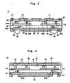
- Fig. 1 is a sectional view of an electronic component embedded board according to the first embodiment of this invention.
- the electronic component embedded board 10 includes a first substrate 11, a second substrate 12, an electronic component 13, a photosensitive resin 14 and conductive members 15, 16.
- the first substrate 11 is a coreless substrate which includes a first multilayered wiring structure 18, protective films 24, 25 and an external connecting terminal 26.
- the first multilayered wiring structure 18 includes insulating layers 27, 31, wirings 28, 29, 33, 34 and vias 30, 32.
- the wirings 28 each are formed on the upper face of the insulating layer 27.
- the wiring 28 is electrically connected to the vias 30, 32.
- the wirings 29 each are formed on the lower face of the insulating layer 27.
- the wiring 29 has a connecting area 29A to which an external connecting terminal 26 is connected.
- the vias 30 each are formed to pass through the insulating layer 27.
- the upper end of the via 30 is connected to the wiring 28.
- the lower end of the via 30 is connected to the wiring 29.
- the via 30 electrically communicates the wirings 28 and 29.
- the insulating layer 31 is formed on the insulating layer 27 so as to cover the wirings 28.
- the vias 32 each are formed so as to pass through the insulating layer 31 located on the wirings 28.
- the via 32 is electrically connected to the wiring 28.
- the wirings 33 each are formed on the upper face of the insulating layer 31.
- the wiring 33 is electrically connected to the via 32.
- the wiring 33 has a connecting area 33A to which the conductive member 16 is connected.
- the wirings 34 each are formed on the upper face of the insulating layer 31 located inside the wirings 33.
- the wirings 34 each have a connecting area 34A to which the conductive member 15 is connected.
- the wiring 34 is electrically connected to the via 32.
- the insulating layers 27, 31 can be made of e.g. epoxy-series resin.
- the wirings 28, 29, 33, 34 and vias 30, 32 can be made of e.g. a conductive metal.
- a concrete example of the conductive metal to be used is Cu.
- the protective film 24 is formed on the insulating layer 31 so as to cover the wirings 33, 34 and expose the connecting areas 33A, 34A.
- the protective film 25 is formed on the lower face of the insulating layer 27 so as to cover the wirings 29 and expose the connecting areas 29A.
- the protective films 24, 25 may be made of e.g. solder resist.
- the external connecting terminal 26 is formed in the connecting area 29A.
- the external connecting terminal 26 is a terminal employed when the electronic component embedded board 10 is connected to a mounting board (not shown) such as a mother board.
- the external connecting terminal 26 may be made of e.g. a solder ball.
- the first substrate 11 constructed as described above is a non-defective substrate for which it has been confirmed that the first multiple-layer structure 18 is free from the malfunction (e.g. opening of the vias, or short-circuiting of the wirings).
- the second substrate 12 is arranged above the first substrate 11, and connected to the first substrate 11 through pillar-shaped conductive members 16.
- the second substrate 12 is a coreless substrate which includes a second multiple-layer structure 41 and protective films 42, 43.
- the second multilayered wiring structure 41 includes insulating layers 45, 51, wirings 46, 47, 53, and vias 49, 52.
- the wirings 46 each are formed on the upper face of the insulating layer 45.
- the wiring 46 is electrically connected to the vias 49, 52.
- the wirings 47 each are formed on the lower face of the insulating layer 45.
- the wiring 47 has a connecting area 47A to which the conductive member 16 is connected.
- the connecting area 47A is connected to the connecting area 33A formed in the first substrate 11.
- the second multilayered wiring structure 41 formed in the second substrate 12 is electrically connected to the first multilayered wiring structure 18.
- the vias 49 each are formed to pass through the insulating layer 45.
- the upper end of the via 49 is connected to the wiring 46.
- the lower end of the via 49 is connected to the wiring 47.
- the via 49 electrically communicates the wirings 46 and 47.
- the insulating layer 51 is formed on the insulating layer 45 so as to cover the wirings 46.
- the vias 52 each are formed so as to pass through the insulating layer 51 located on the wirings 46.
- the via 52 electrically communicates the wirings 46 and 53.
- the wirings 53 each are formed on the upper face of the insulating layer 51.
- the wiring 53 is electrically connected to the via 52.
- the insulating layers 45, 51 can be made of e.g. epoxy-series resin.
- the wirings 46, 47, 53 and vias 49, 52 can be made of e.g. a conductive metal.
- a concrete example of the conductive metal to be used is Cu.
- the protective film 42 is formed on the insulating layer 51 so as to cover the wirings 53.
- the protective film 43 is formed on the lower face of the insulating layer 45 so as to cover the wirings 47 and expose the connecting areas 47A.
- the protective films 42, 43 may be made of e.g. solder resist.
- the second substrate 12 constructed as described above is a non-defective substrate for which it has been confirmed that the second multiple-layer structure 41 is free from the malfunction (e.g. opening of the vias, or short-circuiting of the wirings).
- the electronic component 13 is arranged between the first substrate 11 and the second substrate 12.
- the electronic component 13 has electrode pads 13A.
- the electrode pads 13A each are connected to the connecting area 34A through the conductive member 15.
- the electronic component 13 is electrically connected to the first multilayered wiring structure 18.
- the electronic component may be a chip component (single unit component such as a resistor or capacitor made with a very small size).
- the photosensitive resin 14 is provided between the first substrate 11 and the second substrate 12.
- the photosensitive resin 14 is a photosensitive resin having adhesion (capable of keeping adhesion) even after it has been subjected to exposure and development processing.
- the photosensitive resin 14 seals the electronic component 13 and also bonds the first substrate 11 and the second substrate 12 to each other.
- the photosensitive resin 14 serves to reduce the difference in the thermal expansion coefficient between the first substrate 11 and the second substrate 12 and the difference in the thermal expansion coefficient between the first substrate 11 and the electronic component 13, thereby preventing the first substrate 11, second substrate 12 and electronic component 13 from being broken.
- the photosensitive resin 14 has openings 55 and through holes 56.
- the openings 55 each are formed in the photosensitive resin 14 on the connecting area 34A.
- the opening 55 exposes the connecting area 34A.
- the through holes 56 each are formed so as to pass through the photosensitive resin 14 located between the connecting area 33A and the connecting area 47A.
- the through hole 56 exposes the connecting areas 33A, 47A.
- the through hole 56 is pillar-shaped (e.g. square pillar, cylindrical pillar).
- the space between the first substrate 11 and the second substrate 12 is accurately sealed so that the yield of the electronic component embedded board 10 can be increased.
- the photosensitive resin 14 having adhesion may be e.g. a photosensitive resin film which is a filmy photosensitive resin.
- the photosensitive resin film may be made of e.g. epoxy resin or novolac resin doped with a photoreaction initiator.
- the conductive member 15 is formed in the opening 55.
- the conductive member 15 electrically communicates the electrode pad 13A with the connecting area 34A.
- the conductive member 15 electrically communicates the electronic component 13 with the first multilayered wiring structure 18.
- the conductive member 15 may be made of a conductive material.
- a concrete example of the conductive material is e.g. solder.
- the conductive members 16 each are pillar-shaped (e.g. square pillar or cylindrical pillar) and formed in the through hole 56.
- the conductive member 16 electrically communicates the connecting area 33A with the connecting area 47A.
- the conductive member 16 is a member for electrically connecting the first multilayered wiring structure 18 and the second multilayered wiring structure 41 to each other.
- the conductive member 16 may be made of e.g. solder, or a laminated film composed of Cu, Ni, Au and solder successively stacked on the connecting area 47A.
- the height of the conductive members 16 can be changed according to the electronic component 13.
- various electronic components 13 can be embedded.
- the electronic component embedded board by providing the first substrate 11 having the first multilayered wiring structure 18; and the second substrate 12 having the second multilayered wiring structure 41, before embedding the electronic component 13, the electric test for the first and the second multiple-layer structures 18, 41 can be made.
- the electronic component 13 can be embedded between the first and the second substrates 11, 12 which have been decided as being non-defective products, the yield of the electronic component embedded board 10 can be improved.
- the space between the first and the second substrates 11, 12 can be accurately sealed, thereby improving the yield.
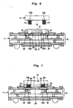
- Figs. 2 to 11 are views showing a manufacturing process of the electronic component embedded board according to the first embodiment of this invention.
- like reference symbols refer to like constituent portions in the electronic component embedded board 10 shown in Fig. 1.
- the first substrate 11 is formed which includes the first multilayered wiring structure 18, protective films 24, 25, and external connecting terminals 26 (first step in claim). Thereafter, an electric test is made for the first substrate 11 with the first multilayered wiring structure 18, thereby providing the first substrate 11 which is a non-defective product.
- the second substrate 12 is formed which includes the second multilayered wiring structure 41 and protective films 42, 43 (second step in claim). Thereafter, an electric test is made for the second substrate 12 with the second multilayered wiring structure 41, thereby providing the second substrate 12 which is a non-defective product.
- a first photosensitive resin 61 having adhesion is formed so as to cover the upper face of the first substrate 11 (the face on the side where the protective film 24 and the connecting areas 33A, 34A are formed).
- the photosensitive resin film having adhesion is affixed to the upper face of the first substrate 11.
- the photosensitive resin film may be made of e.g. epoxy resin or novolac resin doped with a photoreaction initiator.
- the photosensitive resin film can have a thickness of e.g. 30 ⁇ m to 50 ⁇ m.
- the first photosensitive resin 61 is a photosensitive resin having adhesion (capable of keeping adhesion) even after it has been subjected to exposure and development processing.
- the first photosensitive resin 61 can be easily formed as compared with the case where a liquid photosensitive resin having adhesion is used.
- the first photosensitive resin 61 is subjected to exposure and development processing to form the openings 55 exposing the connecting areas 34A and remove the first photosensitive resin 61 formed on the area other than an electronic component arranging region A.
- the electronic component arranging area A refers to a region on the first photosensitive resin 61 in contact with the electronic component 13.
- the conductive members 15 are formed on the electrode pads 13A of the electronic component 13.
- pillar-shaped solders are formed on the electrode pads 13A of the electronic component 13.
- the electronic component 13 is bonded to the first photosensitive resin 61 having adhesion.
- the conductive members 15 being inserted in the openings 55, by heating, the conductive members 15 are molten to connect the conductive members 15 to the connecting areas 34A (third step in claim).
- the electronic component 13 is electrically connected to the first multiple-layer structure 18.
- the heating condition in melting the conductive members 15 can be set as the temperature of 230 to 250°C and the heating time of about several seconds to 10 seconds.
- a second photosensitive resin 62 having adhesion is formed so as to cover the upper face of the structure shown in Fig. 7 (fourth step in claim).
- the photosensitive resin film is affixed to the upper face of the structure of the structure shown in Fig. 7.
- the photosensitive resin film may be made of e.g. epoxy resin or novolac resin doped with a photo initiator.
- the thickness of the photosensitive resin film may be 100 ⁇ m in the case where the thickness of the electronic component 13 is 50 ⁇ m.
- the second photosensitive resin 62 is a photosensitive resin having adhesion (capable of keeping adhesion) even after it has been subjected to exposure and development processing. Further, after the photosensitive resin film has been affixed, a plate having a flat plane may be pressed on the upper face of the photosensitive resin film to make the upper face of the photosensitive resin film flat.
- the second photosensitive resin 62 can be easily formed as compared with the case where a liquid photosensitive resin having adhesion is used.
- the second photosensitive resin 62 is subjected to exposure and development processing to form the through holes 56 exposing the connecting areas 33A.
- the first photosensitive resin 61 having the openings 55 and the second photosensitive resin 62 having the through holes 56 are formed.
- the conductive members 16 are formed in the connecting areas 47A of the second substrate 12 (conductive member forming step).
- the solder or a laminated film composed of Cu, Ni, Au and solder successively stacked on the connecting area 47A is formed.
- Cu, Ni and Au constituting the laminated film can be formed by plating, respectively.
- the second substrate 12 is bonded to the second photosensitive resin 62 having adhesion.
- the conductive members 16 are molten to connect the conductive members 16 to the connecting areas 33A (fifth step in claim).
- the second multilayered wiring structure 41 is electrically connected to the first multilayered wiring structure 18, thus completing the electronic component embedded board 10.
- the heating condition in melting the solder of the conductive members 16 can be set as for example, the temperature of 230 to 250°C and the heating time of about several seconds to 10 seconds.
- the yield of the electronic component embedded board 10 can be improved.
- the space between the first substrate 11 and the second substrate 12 can be accurately sealed as compared with the case where an underfill resin is formed between the first substrate and the second substrate by capillary phenomenon.
- the yield of the electronic component embedded board 10 can be improved.
- the photosensitive resin film as the photosensitive resin 14 having adhesion, the photosensitive resin 14 can be easily formed in a short time.
- the concrete example of the photosensitive resin 14 was explained as an example using the photosensitive resin film.
- the liquid photosensitive resin having adhesion may be applied.
- the liquid photosensitive resin can be formed by e.g. spin coating.
- the photosensitive resin having adhesion was explained as an example of the resin sealing the electric component and bonding the first substrate and the second substrate to each other.
- a nonconductive resin or an anisotropic conductive resin may be applied.
- the nonconductive resin or the anisotropic conductive resin may be e.g. NCF(nonconductive film), NCP(nonconductive paste), ACF(anisotropic conductive film) or ACP(anisotropic conductive paste).
- the processes in Figs. 5 and 9, i.e., the processes of making the openings 55 and through holes 56 in the first and second resins may be omitted. More specifically, the electric component 13 with the conductive member 15 is pressed against the first resin applied on the first substrate 11 so that the conductive member 15 passes through the first resin and then connects to the connecting areas 34A, and then the first resin is cured. Similarly, the second substrate 12 with the conductive member 16 is pressed against the second resin applied on the structure as shown in Fig. 7 so that the conductive member 16 passes through the second resin and then connects to the connecting areas 33A, and then the second resin is cured.
- an underfill resin may be applied between the first substrate 11 and the second substrate 12 by capillary phenomenon.
- the underfill resin may be made of e.g. epoxy resin.
- the underfill resin is applied between the first substrate 11 and the second substrate 12 in a state that the electronic component 13 with the conductive member 15 and the second substrate 12 with the conductive member 16 are provided on the first substrate 11, and then the underfill resin is cured.
- NCF NCF
- NCP NCP
- ACF ACP
- ACP underfill resin
- first and the second substrates 11, 12 were explained as an example using the coreless substrates.
- wiring boards having core substrates may be employed as the first and the second substrates 11, 12. In this case also, the same effect as in this embodiment can be obtained.
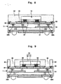
- Fig. 12 is a sectional view of the electronic component embedded board according to the second embodiment of this invention.
- like reference symbols refer to like constituent portions in the electronic component embedded board 10 according to the first embodiment.
- the reference symbols for constituent elements in the electronic component embedded board 10 are given "-1"
- the reference symbols for the constituent elements of the structure provided on the electronic component embedded board 10 are given "-2".
- an electronic component embedded board 70 further includes, on the electronic component embedded board 10 explained in the first embodiment, a second substrate 12-2, an electronic component 13-2, a photosensitive resin 14-2 having adhesion, and conductive members 15-2, 16-2.
- the second substrate 12-2 is arranged above the second substrate 12-1 and has a second multilayered wiring structure 41-2.
- the second multilayered wiring structure 41-2 is electrically connected to the second multilayered wiring structure 41-1 of the second substrate 12-1 through the pillar-shaped conductive members 16-2.
- the electronic component 13-2 is arranged between the second substrate 12-1 and the second substrate 12-2.
- the electronic component 13-2 has electrode pads 13A-2.
- the electrode pads 13A-2 are electrically connected to wirings 53-1 through the conductive members 15-2, respectively.
- the electronic component 13-2 is electrically connected to the second multilayered wiring structure 41-1.
- the photosensitive resin 14-2 is arranged between the second substrate 12-1 and the second substrate 12-2.
- the photosensitive resin 14-2 seals the electronic component 13-2 and also bonds the second substrate 12-1 and the second substrate 12-2 to each other.
- the photosensitive resin 14-2 has openings 55-2 and through holes 56-2.
- the openings 55-2 and the through holes 56-2 are made in the photosensitive resin 14-2 formed on the wirings 53-1.
- the openings 55-2 each expose the wiring 53-1 and the through holes 56-2 each expose the wring 53-1 and a connecting area 47A-2.
- the conductive member 15-2 is formed in the opening 55-2, and electrically communicates the electrode pad 13A-2 with the wiring 53-1.
- the conductive member 16-2 is formed in the through hole 56-2 and electrically communicates the wiring 53-1 with the connecting area 47A-2.
- the electronic component embedded board 70 in which three substrates 11, 12-1, 12-2 are stacked so that the electronic components 13-1, 13-2 are arranged between the substrates adjacent to each other in a vertical direction (in this embodiment, between the first substrate 11 and the second substrate 12-1 and between the second substrate 12-1 and the second substrate 12-2) and the substrates adjacent to each other in the vertical direction are bonded by the photosensitive resins 14-1, 14-2 having adhesion, the same effect as in the electronic component embedded board 10 according to the first embodiment can be obtained.
- the case where the three substrates 11, 12-1, 12-2 are stacked was adopted.
- the electronic component embedded board in which three or more substrates are stacked so that the electronic components 13 are arranged between the substrates adjacent in the vertical direction and the substrates adjacent in the vertical direction are bonded by the photosensitive resins 14 having adhesion the same effect as in the electronic component embedded board 10 can be obtained.
- the photosensitive resin having adhesion was explained as an example of the resin sealing the electric component and bonding the first substrate and the second substrate to each other.
- NCF, NCP, ACF, ACP or underfill resin can be used.
- the electronic component embedded board 70 can be manufactured in the same method as the method for manufacturing the electronic component embedded board 10 according to the first embodiment as described previously.
- This invention is applicable to the electronic component embedded board and its manufacturing method capable of the yield.
Abstract
Description
- The present disclosure relates to a board embedding an electronic component (referred to as an electronic component embedded board) and its manufacturing method, and more particularly to an electronic component embedded board embedding an electronic component in a substrate having a multilayered wiring structure and its manufacturing method.
- In recent years, high density of an electronic component such as a semiconductor chip has greatly advanced, thereby downsizing the electronic component. Correspondingly, there has been proposed an electronic component embedded board embedding an electronic component in a substrate having a multilayered wiring structure in which a plurality of insulating layers, wirings and vias are stacked.
- Fig. 13 is a sectional view of a related-art electronic component embedded board.
- As shown in Fig. 13, an electronic component embedded
board 100 includes asubstrate 101 and anelectronic component 113. Thesubstrate 101 has acore substrate 102,wirings 104 provided on thecore substrate 102 and amultilayered wiring structure 103. - The
multilayered wiring structure 103 is formed on thecore substrate 102 with thewirings 104. Themultilayered wiring structure 103 includes insulating layers 106 to 108 stacked on thecore substrate 102,wirings 109 to 111 formed on the insulating layers 106 to 108, respectively, and vias (not shown) made in the insulating layers and electrically connecting thesewirings 109 to 111. - The
electronic component 113 is formed on thewirings 104 and connected thereto. Theelectronic component 113 is covered with theinsulating layers 106 and 107. - In the electronic component embedded
board 100 having such a configuration, after thewirings 104 have been formed on thecore substrate 102, theelectronic component 113 is connected onto thewirings 104. Thereafter, the insulating layers 106 to 108,wirings 109 to 111 and vias (not shown), which constitute themultilayered wiring structure 103, are formed (for example, seeJapanese Patent Unexamined Publication No. Hei. 11-274734 - However, in a related-art electronic component embedded
board 100, after theelectronic component 113 has been connected to thewirings 104, the multiple-layer structure 103 is formed. Therefore, even where there is no problem in electric connection between theelectronic component 113 and thewirings 104, if a malfunction (e.g. opening of the vias, or short-circuiting of the wirings) occurs in thewirings 109 to 111 and vias (not shown), the problem of reduction in the yield of the electronic component embeddedboard 100 was presented. - Embodiments of the present invention provide an electronic component embedded board capable of improving the yield and a method for manufacturing the same.
- In light of the above, the electronic component embedded board according to
independent claim 1, and the method of manufacturing thereof according toindependent claims 6 and 11 are provided. Further advantages, features, aspects and details of the invention are evident from the dependent claims, the description and the drawings. - According to an aspect of one or more embodiments of the invention, there is provided with an electronic component embedded board comprising: a first substrate having a first multi-layer wiring structure; a second substrate having a second multilayered wiring structure and being provided above the first substrate; an electronic component arranged between the first substrate and the second substrate; and a resin being arranged between the first substrate and the second substrate, and sealing the electronic component and bonding the first substrate and the second substrate to each other.
- The resin may be a photosensitive resin having adhesion, underfill resin, nonconductive resin or anisotropic conductive resin.
- In accordance with this invention, by providing a first substrate having a first multi-layer wiring structure, and a second substrate having a second multilayered wiring structure, before embedding an electronic component, an electric test for the first and the second multiple-layer structure can be made. Thus, since the electronic component can be embedded between the first and the second substrate which have been decided as being non-defective products, the yield of the electronic component embedded board can be improved.
- By providing a photosensitive resin having adhesion between the first and the second substrate, the space between the first and the second substrates can be accurately sealed, thereby improving the yield.
- By providing an underfill resin, nonconductive resin or anisotropic conductive resin, the commonly used resin and the commonly used production line can be used.
- According to an aspect of one or more embodiments of the invention, there is provided a method for manufacturing an electronic component embedded board, comprising: a first step of forming a first substrate having a first multilayered wiring structure; a second step of forming a second substrate having a second multilayered wiring structure; a third step of electrically connecting an electronic component and the first multilayered wiring structure by bonding the electronic component to the first substrate using a first resin; a fourth step of forming a second resin so as to cover a surface of the first substrate with the electronic component arranged thereon and the electronic component; and a fifth step of arranging the second substrate above the first substrate by bonding the second substrate onto the second resin.
- The resin may be a photosensitive resin having adhesion, nonconductive resin or anisotropic conductive resin.
- According to another aspect of one or more embodiments of the invention, there is provided a method for manufacturing an electronic component embedded board, comprising: a first step of forming a first substrate having a first multilayered wiring structure; a second step of forming a second substrate having a second multilayered wiring structure; a third step of electrically connecting an electronic component and the first multilayered wiring structure; a fourth step of arranging the second substrate above the first substrate; and a fifth step of applying an underfill resin between the first substrate and the second substrate.
- In accordance with this invention, after having provided a first substrate having a first multilayered wiring structure; and a second substrate having a second multilayered wiring structure, by making an electric test for the first and the second multiple-layer structures and embedding the electronic component between the first and the second substrate which have been decided as being non-defective products, the yield of the electronic component embedded board can be improved.
- Further, by bonding the electronic component to the first substrate using the first photosensitive resin having adhesion, and forming a second photosensitive resin having adhesion so as to cover a surface of the first substrate with the electronic component arranged thereon and the electronic component, the space between the first and the second substrates can be accurately sealed, thereby improving the yield of the electronic component embedded board.
- By providing an underfill resin, nonconductive resin or anisotropic conductive resin, the commonly used resin and the commonly used production line can be used.
- Embodiments according to the invention are also directed to methods with method steps, which may be performed by way of hardware components, a computer programmed by appropriate software, by any combination of the two or in any other manner. Furthermore, embodiments according to the invention are also directed to methods by which the described apparatuses are manufactured. It includes method steps for manufacturing every part of the apparatus.
- Various implementations may include one or more the following advantages. For example, the yield of the electronic component embedded board can be improved.
- Other features and advantages may be apparent from the following detailed description, the accompanying drawings and the claims.
- Fig. 1 is a sectional view of an electronic component embedded board according to the first embodiment of this invention.
- Fig. 2 is a view showing the process of manufacturing an electronic component embedded board according to the first embodiment of this invention (first step).
- Fig. 3 is a view showing the process of manufacturing an electronic component embedded board according to the first embodiment of this invention (second step).
- Fig. 4 is a view showing the process of manufacturing an electronic component embedded board according to the first embodiment of this invention (third step).
- Fig. 5 is a view showing the process of manufacturing an electronic component embedded board according to the first embodiment of this invention (fourth step).
- Fig. 6 is a view showing the process of manufacturing an electronic component embedded board according to the first embodiment of this invention (fifth step).
- Fig. 7 is a view showing the process of manufacturing an electronic component embedded board according to the first embodiment of this invention (sixth step).
- Fig. 8 is a view showing the process of manufacturing an electronic component embedded board according to the first embodiment of this invention (seventh step).
- Fig. 9 is a view showing the process of manufacturing an electronic component embedded board according to the first embodiment of this invention (eighth step).
- Fig. 10 is a view showing the process of manufacturing an electronic component embedded board according to the first embodiment of this invention (ninth step).
- Fig. 11 is a view showing the process of manufacturing an electronic component embedded board according to the first embodiment of this invention (tenth step).
- Fig. 12 is a sectional view of an electronic component embedded board according to the second embodiment of this invention
- Fig. 13 is a sectional view of a related-art electronic component embedded board.
- Now referring to the drawings, an explanation will be given of various embodiments of this invention.
- Fig. 1 is a sectional view of an electronic component embedded board according to the first embodiment of this invention.
- Referring to Fig. 1, an explanation will be given of an electronic component embedded
board 10 according to the first embodiment of this invention. The electronic component embeddedboard 10 includes afirst substrate 11, asecond substrate 12, anelectronic component 13, aphotosensitive resin 14 andconductive members - The
first substrate 11 is a coreless substrate which includes a firstmultilayered wiring structure 18,protective films external connecting terminal 26. - The first
multilayered wiring structure 18 includesinsulating layers wirings vias wirings 28 each are formed on the upper face of theinsulating layer 27. Thewiring 28 is electrically connected to thevias wirings 29 each are formed on the lower face of theinsulating layer 27. Thewiring 29 has a connectingarea 29A to which an external connectingterminal 26 is connected. Thevias 30 each are formed to pass through theinsulating layer 27. The upper end of thevia 30 is connected to thewiring 28. The lower end of thevia 30 is connected to thewiring 29. Thevia 30 electrically communicates thewirings - The
insulating layer 31 is formed on theinsulating layer 27 so as to cover thewirings 28. Thevias 32 each are formed so as to pass through theinsulating layer 31 located on thewirings 28. The via 32 is electrically connected to thewiring 28. Thewirings 33 each are formed on the upper face of the insulatinglayer 31. Thewiring 33 is electrically connected to the via 32. Thewiring 33 has a connectingarea 33A to which theconductive member 16 is connected. Thewirings 34 each are formed on the upper face of the insulatinglayer 31 located inside thewirings 33. Thewirings 34 each have a connectingarea 34A to which theconductive member 15 is connected. Thewiring 34 is electrically connected to the via 32. - The insulating layers 27, 31 can be made of e.g. epoxy-series resin. The
wirings vias - The
protective film 24 is formed on the insulatinglayer 31 so as to cover thewirings areas protective film 25 is formed on the lower face of the insulatinglayer 27 so as to cover thewirings 29 and expose the connectingareas 29A. Theprotective films - The external connecting
terminal 26 is formed in the connectingarea 29A. The external connectingterminal 26 is a terminal employed when the electronic component embeddedboard 10 is connected to a mounting board (not shown) such as a mother board. The external connectingterminal 26 may be made of e.g. a solder ball. - The
first substrate 11 constructed as described above is a non-defective substrate for which it has been confirmed that the first multiple-layer structure 18 is free from the malfunction (e.g. opening of the vias, or short-circuiting of the wirings). - The
second substrate 12 is arranged above thefirst substrate 11, and connected to thefirst substrate 11 through pillar-shapedconductive members 16. Thesecond substrate 12 is a coreless substrate which includes a second multiple-layer structure 41 andprotective films - The second
multilayered wiring structure 41 includes insulatinglayers wirings 46 each are formed on the upper face of the insulatinglayer 45. Thewiring 46 is electrically connected to thevias wirings 47 each are formed on the lower face of the insulatinglayer 45. Thewiring 47 has a connectingarea 47A to which theconductive member 16 is connected. The connectingarea 47A is connected to the connectingarea 33A formed in thefirst substrate 11. Thus, the secondmultilayered wiring structure 41 formed in thesecond substrate 12 is electrically connected to the firstmultilayered wiring structure 18. - The
vias 49 each are formed to pass through the insulatinglayer 45. The upper end of the via 49 is connected to thewiring 46. The lower end of the via 49 is connected to thewiring 47. The via 49 electrically communicates thewirings - The insulating
layer 51 is formed on the insulatinglayer 45 so as to cover thewirings 46. Thevias 52 each are formed so as to pass through the insulatinglayer 51 located on thewirings 46. The via 52 electrically communicates thewirings wirings 53 each are formed on the upper face of the insulatinglayer 51. Thewiring 53 is electrically connected to the via 52. - The insulating layers 45, 51 can be made of e.g. epoxy-series resin. The
wirings vias - The
protective film 42 is formed on the insulatinglayer 51 so as to cover thewirings 53. Theprotective film 43 is formed on the lower face of the insulatinglayer 45 so as to cover thewirings 47 and expose the connectingareas 47A. Theprotective films - The
second substrate 12 constructed as described above is a non-defective substrate for which it has been confirmed that the second multiple-layer structure 41 is free from the malfunction (e.g. opening of the vias, or short-circuiting of the wirings). - The
electronic component 13 is arranged between thefirst substrate 11 and thesecond substrate 12. Theelectronic component 13 haselectrode pads 13A. Theelectrode pads 13A each are connected to the connectingarea 34A through theconductive member 15. Thus, theelectronic component 13 is electrically connected to the firstmultilayered wiring structure 18. The electronic component may be a chip component (single unit component such as a resistor or capacitor made with a very small size). - The
photosensitive resin 14 is provided between thefirst substrate 11 and thesecond substrate 12. Thephotosensitive resin 14 is a photosensitive resin having adhesion (capable of keeping adhesion) even after it has been subjected to exposure and development processing. Thephotosensitive resin 14 seals theelectronic component 13 and also bonds thefirst substrate 11 and thesecond substrate 12 to each other. In addition, thephotosensitive resin 14 serves to reduce the difference in the thermal expansion coefficient between thefirst substrate 11 and thesecond substrate 12 and the difference in the thermal expansion coefficient between thefirst substrate 11 and theelectronic component 13, thereby preventing thefirst substrate 11,second substrate 12 andelectronic component 13 from being broken. - The
photosensitive resin 14 hasopenings 55 and throughholes 56. Theopenings 55 each are formed in thephotosensitive resin 14 on the connectingarea 34A. Theopening 55 exposes the connectingarea 34A. The through holes 56 each are formed so as to pass through thephotosensitive resin 14 located between the connectingarea 33A and the connectingarea 47A. The throughhole 56 exposes the connectingareas hole 56 is pillar-shaped (e.g. square pillar, cylindrical pillar). - In this way, by providing the
photosensitive resin 14 having adhesion between thefirst substrate 11 and thesecond substrate 12, the space between thefirst substrate 11 and thesecond substrate 12 is accurately sealed so that the yield of the electronic component embeddedboard 10 can be increased. - The
photosensitive resin 14 having adhesion may be e.g. a photosensitive resin film which is a filmy photosensitive resin. The photosensitive resin film may be made of e.g. epoxy resin or novolac resin doped with a photoreaction initiator. - The
conductive member 15 is formed in theopening 55. Theconductive member 15 electrically communicates theelectrode pad 13A with the connectingarea 34A. Theconductive member 15 electrically communicates theelectronic component 13 with the firstmultilayered wiring structure 18. Theconductive member 15 may be made of a conductive material. A concrete example of the conductive material is e.g. solder. - The
conductive members 16 each are pillar-shaped (e.g. square pillar or cylindrical pillar) and formed in the throughhole 56. Theconductive member 16 electrically communicates the connectingarea 33A with the connectingarea 47A. Theconductive member 16 is a member for electrically connecting the firstmultilayered wiring structure 18 and the secondmultilayered wiring structure 41 to each other. Theconductive member 16 may be made of e.g. solder, or a laminated film composed of Cu, Ni, Au and solder successively stacked on the connectingarea 47A. - As described above, by providing the pillar-shaped
conductive members 16 between thefirst substrate 11 and thesecond substrate 12 so that thefirst substrate 11 and thesecond substrate 12 are electrically connected to each other through theconductive members 16, the height of theconductive members 16 can be changed according to theelectronic component 13. Thus, variouselectronic components 13 can be embedded. - In accordance with the electronic component embedded board according to this invention, by providing the
first substrate 11 having the firstmultilayered wiring structure 18; and thesecond substrate 12 having the secondmultilayered wiring structure 41, before embedding theelectronic component 13, the electric test for the first and the second multiple-layer structures electronic component 13 can be embedded between the first and thesecond substrates board 10 can be improved. - By providing the
photosensitive resin 14 having adhesion between the first and thesecond substrates second substrates - Figs. 2 to 11 are views showing a manufacturing process of the electronic component embedded board according to the first embodiment of this invention. In Figs. 2 to 11, like reference symbols refer to like constituent portions in the electronic component embedded
board 10 shown in Fig. 1. - First, as shown in Fig. 2, using a known technique, the
first substrate 11 is formed which includes the firstmultilayered wiring structure 18,protective films first substrate 11 with the firstmultilayered wiring structure 18, thereby providing thefirst substrate 11 which is a non-defective product. - Next, as shown in Fig. 3, the
second substrate 12 is formed which includes the secondmultilayered wiring structure 41 andprotective films 42, 43 (second step in claim). Thereafter, an electric test is made for thesecond substrate 12 with the secondmultilayered wiring structure 41, thereby providing thesecond substrate 12 which is a non-defective product. - Next, as shown in Fig. 4, a first
photosensitive resin 61 having adhesion is formed so as to cover the upper face of the first substrate 11 (the face on the side where theprotective film 24 and the connectingareas photosensitive resin 61, the photosensitive resin film having adhesion is affixed to the upper face of thefirst substrate 11. The photosensitive resin film may be made of e.g. epoxy resin or novolac resin doped with a photoreaction initiator. The photosensitive resin film can have a thickness of e.g. 30 µm to 50 µm. The firstphotosensitive resin 61 is a photosensitive resin having adhesion (capable of keeping adhesion) even after it has been subjected to exposure and development processing. - In this way, by using the photosensitive resin film having adhesion as the first
photosensitive resin 61, the firstphotosensitive resin 61 can be easily formed as compared with the case where a liquid photosensitive resin having adhesion is used. - Next, as shown in Fig. 5, the first
photosensitive resin 61 is subjected to exposure and development processing to form theopenings 55 exposing the connectingareas 34A and remove the firstphotosensitive resin 61 formed on the area other than an electronic component arranging region A. The electronic component arranging area A refers to a region on the firstphotosensitive resin 61 in contact with theelectronic component 13. - Next, as shown in Fig. 6, the
conductive members 15 are formed on theelectrode pads 13A of theelectronic component 13. Concretely, pillar-shaped solders are formed on theelectrode pads 13A of theelectronic component 13. - Next, as shown in Fig. 7, the
electronic component 13 is bonded to the firstphotosensitive resin 61 having adhesion. In addition, with theconductive members 15 being inserted in theopenings 55, by heating, theconductive members 15 are molten to connect theconductive members 15 to the connectingareas 34A (third step in claim). Thus, theelectronic component 13 is electrically connected to the first multiple-layer structure 18. The heating condition in melting theconductive members 15 can be set as the temperature of 230 to 250°C and the heating time of about several seconds to 10 seconds. - Next, as shown in Fig. 8, a second
photosensitive resin 62 having adhesion is formed so as to cover the upper face of the structure shown in Fig. 7 (fourth step in claim). Concretely, as the secondphotosensitive resin 62, the photosensitive resin film is affixed to the upper face of the structure of the structure shown in Fig. 7. The photosensitive resin film may be made of e.g. epoxy resin or novolac resin doped with a photo initiator. The thickness of the photosensitive resin film may be 100 µm in the case where the thickness of theelectronic component 13 is 50 µm. - The second
photosensitive resin 62 is a photosensitive resin having adhesion (capable of keeping adhesion) even after it has been subjected to exposure and development processing. Further, after the photosensitive resin film has been affixed, a plate having a flat plane may be pressed on the upper face of the photosensitive resin film to make the upper face of the photosensitive resin film flat. - In this way, by using the photosensitive resin film having adhesion as the second
photosensitive resin 62, the secondphotosensitive resin 62 can be easily formed as compared with the case where a liquid photosensitive resin having adhesion is used. - Next, as shown in Fig. 9, the second
photosensitive resin 62 is subjected to exposure and development processing to form the throughholes 56 exposing the connectingareas 33A. Thus, the firstphotosensitive resin 61 having theopenings 55 and the secondphotosensitive resin 62 having the throughholes 56 are formed. - Next, as shown in Fig. 10, the
conductive members 16 are formed in the connectingareas 47A of the second substrate 12 (conductive member forming step). Concretely, in the connectingarea 47A of thesecond substrate 12, as theconductive members 16, the solder or a laminated film composed of Cu, Ni, Au and solder successively stacked on the connectingarea 47A is formed. Cu, Ni and Au constituting the laminated film can be formed by plating, respectively. - Next, as shown in Fig. 11, the
second substrate 12 is bonded to the secondphotosensitive resin 62 having adhesion. In addition, with theconductive members 16 being inserted in the throughholes 56, by heating, theconductive members 16 are molten to connect theconductive members 16 to the connectingareas 33A (fifth step in claim). Thus, the secondmultilayered wiring structure 41 is electrically connected to the firstmultilayered wiring structure 18, thus completing the electronic component embeddedboard 10. The heating condition in melting the solder of theconductive members 16 can be set as for example, the temperature of 230 to 250°C and the heating time of about several seconds to 10 seconds. - In accordance with the method for manufacturing an electronic component embedded board, after having provided the
first substrate 11 having the firstmulti-layer wiring structure 18, and thesecond substrate 12 having the secondmultilayered wiring structure 41, by making an electric test for the first and thesecond substrates second substrates board 10 can be improved. - Further, by using the
photosensitive resin 14 having adhesion, for example, the space between thefirst substrate 11 and thesecond substrate 12 can be accurately sealed as compared with the case where an underfill resin is formed between the first substrate and the second substrate by capillary phenomenon. Thus, the yield of the electronic component embeddedboard 10 can be improved. - Further, even where the size (area) in a surface-direction of the first and the
second substrates first substrate 11 and thesecond substrate 12 can be accurately sealed. Further, by using the photosensitive resin film as thephotosensitive resin 14 having adhesion, thephotosensitive resin 14 can be easily formed in a short time. - In this embodiment, the concrete example of the
photosensitive resin 14 was explained as an example using the photosensitive resin film. However, in place of the photosensitive resin film, the liquid photosensitive resin having adhesion may be applied. The liquid photosensitive resin can be formed by e.g. spin coating. - Further, in this embodiment, the photosensitive resin having adhesion was explained as an example of the resin sealing the electric component and bonding the first substrate and the second substrate to each other. However, in place of the photosensitive resin having adhesion, a nonconductive resin or an anisotropic conductive resin may be applied. The nonconductive resin or the anisotropic conductive resin may be e.g. NCF(nonconductive film), NCP(nonconductive paste), ACF(anisotropic conductive film) or ACP(anisotropic conductive paste).
- In a case of using the nonconductive resin or anisotropic conductive resin, the processes in Figs. 5 and 9, i.e., the processes of making the
openings 55 and throughholes 56 in the first and second resins may be omitted. More specifically, theelectric component 13 with theconductive member 15 is pressed against the first resin applied on thefirst substrate 11 so that theconductive member 15 passes through the first resin and then connects to the connectingareas 34A, and then the first resin is cured. Similarly, thesecond substrate 12 with theconductive member 16 is pressed against the second resin applied on the structure as shown in Fig. 7 so that theconductive member 16 passes through the second resin and then connects to the connectingareas 33A, and then the second resin is cured. - Further, in place of the photosensitive resin having adhesion, an underfill resin may be applied between the
first substrate 11 and thesecond substrate 12 by capillary phenomenon. The underfill resin may be made of e.g. epoxy resin. In a case of using the underfill resin, the underfill resin is applied between thefirst substrate 11 and thesecond substrate 12 in a state that theelectronic component 13 with theconductive member 15 and thesecond substrate 12 with theconductive member 16 are provided on thefirst substrate 11, and then the underfill resin is cured. - By using NCF, NCP, ACF, ACP or underfill resin, in place of the photosensitive resin having adhesion, the commonly used resin or commonly used production line can be used.
- In this embodiment, the first and the
second substrates second substrates - Fig. 12 is a sectional view of the electronic component embedded board according to the second embodiment of this invention. In Fig. 12, like reference symbols refer to like constituent portions in the electronic component embedded
board 10 according to the first embodiment. Incidentally, in Fig. 12, for convenience for explanation, the reference symbols for constituent elements in the electronic component embeddedboard 10 are given "-1", and the reference symbols for the constituent elements of the structure provided on the electronic component embeddedboard 10 are given "-2". - As shown in Fig. 12, an electronic component embedded
board 70 further includes, on the electronic component embeddedboard 10 explained in the first embodiment, a second substrate 12-2, an electronic component 13-2, a photosensitive resin 14-2 having adhesion, and conductive members 15-2, 16-2. - The second substrate 12-2 is arranged above the second substrate 12-1 and has a second multilayered wiring structure 41-2. The second multilayered wiring structure 41-2 is electrically connected to the second multilayered wiring structure 41-1 of the second substrate 12-1 through the pillar-shaped conductive members 16-2.
- The electronic component 13-2 is arranged between the second substrate 12-1 and the second substrate 12-2. The electronic component 13-2 has
electrode pads 13A-2. Theelectrode pads 13A-2 are electrically connected to wirings 53-1 through the conductive members 15-2, respectively. Thus, the electronic component 13-2 is electrically connected to the second multilayered wiring structure 41-1. - The photosensitive resin 14-2 is arranged between the second substrate 12-1 and the second substrate 12-2. The photosensitive resin 14-2 seals the electronic component 13-2 and also bonds the second substrate 12-1 and the second substrate 12-2 to each other. The photosensitive resin 14-2 has openings 55-2 and through holes 56-2. The openings 55-2 and the through holes 56-2 are made in the photosensitive resin 14-2 formed on the wirings 53-1. The openings 55-2 each expose the wiring 53-1 and the through holes 56-2 each expose the wring 53-1 and a connecting
area 47A-2. - The conductive member 15-2 is formed in the opening 55-2, and electrically communicates the
electrode pad 13A-2 with the wiring 53-1. The conductive member 16-2 is formed in the through hole 56-2 and electrically communicates the wiring 53-1 with the connectingarea 47A-2. - As described above, also in the electronic component embedded
board 70 in which threesubstrates 11, 12-1, 12-2 are stacked so that the electronic components 13-1, 13-2 are arranged between the substrates adjacent to each other in a vertical direction (in this embodiment, between thefirst substrate 11 and the second substrate 12-1 and between the second substrate 12-1 and the second substrate 12-2) and the substrates adjacent to each other in the vertical direction are bonded by the photosensitive resins 14-1, 14-2 having adhesion, the same effect as in the electronic component embeddedboard 10 according to the first embodiment can be obtained. - In this embodiment, the case where the three
substrates 11, 12-1, 12-2 are stacked was adopted. However, also in the electronic component embedded board in which three or more substrates are stacked so that theelectronic components 13 are arranged between the substrates adjacent in the vertical direction and the substrates adjacent in the vertical direction are bonded by thephotosensitive resins 14 having adhesion, the same effect as in the electronic component embeddedboard 10 can be obtained. - Further, in this embodiment, the photosensitive resin having adhesion was explained as an example of the resin sealing the electric component and bonding the first substrate and the second substrate to each other. However, in place of the photosensitive resin having adhesion, NCF, NCP, ACF, ACP or underfill resin can be used.
- Further, the electronic component embedded
board 70 can be manufactured in the same method as the method for manufacturing the electronic component embeddedboard 10 according to the first embodiment as described previously. - Hitherto, the preferred embodiments of this invention have been explained in detail. However, this invention should not be limited to these specific embodiments but may be modified or changed in various manners within a scope of the spirit of this invention described in claims.
- This invention is applicable to the electronic component embedded board and its manufacturing method capable of the yield.
Claims (11)
- An electronic component embedded board (10, 70) comprising:a first substrate (11) having a first multi-layer wiring structure;a second substrate (12; 12-1, 12-2) having a second multilayered wiring structure and being provided above said first substrate;a electronic component (13; 13-1, 13-2) arranged between said first substrate and said second substrate; anda resin (14; 14-1, 14-2) being arranged between said first substrate and said second substrate, and sealing said electronic component and bonding said first substrate and said second substrate to each other.
- An electronic component embedded board according to claim 1, wherein the resin is a photosensitive resin having adhesion.
- An electronic component embedded board according to claim 1, wherein the resin is an underfill resin.
- An electronic component embedded board according to claim 1, wherein the resin is a nonconductive resin or anisotropic conductive resin.
- An electronic component embedded board according to any of claims 1 to 4, further comprising:a pillar-shaped conductive member (16; 16-2) being arranged between said first substrate and said second substrate and electrically connecting said first multiple-layer structure and said second multiple-layer structure.
- A method for manufacturing an electronic component embedded board (10; 70), comprising:a first step of forming a first substrate (11) having a first multilayered wiring structure;a second step of forming a second substrate (12; 12-1, 12-2) having a second multilayered wiring structure;a third step of electrically connecting an electronic component and said first multilayered wiring structure by bonding said electronic component to said first substrate using a first resin;a fourth step of forming a second resin so as to cover a surface of said first substrate with said electronic component arranged thereon and said electronic component; anda fifth step of arranging said second substrate above said first substrate by bonding said second substrate onto said second resin.
- A method for manufacturing an electronic component embedded board according to claim 6, wherein the first and second resins are photosensitive resins having adhesion.
- A method for manufacturing an electronic component embedded board according to claim 6, wherein the first and second resins are nonconductive resins or anisotopic conductive resins.
- A method for manufacturing an electronic component embedded board according to any of claims 6 to 8, wherein said fifth step includes a step of forming between said first substrate (11) and said second substrate (12; 12-1, 12-2)a pillar-shaped conductive member (16; 16-2) for electrically connecting said first multiple-layer structure and said second multiple-layer structure.
- A method for manufacturing an electronic component embedded boar according to claim 7, wherein said first and said second photosensitive resins are photosensitive resin films.
- A method for manufacturing an electronic component embedded board (10, 70), comprising:a first step of forming a first substrate (11) having a first multilayered wiring structure;a second step of forming a second substrate (12; 12-1, 12-2) having a second multilayered wiring structure;a third step of electrically connecting an electronic component and said first multilayered wiring structure;a fourth step of arranging said second substrate above said first substrate; anda fifth step of applying an underfill resin between the first substrate and the second substrate.
Applications Claiming Priority (1)
| Application Number | Priority Date | Filing Date | Title |
|---|---|---|---|
| JP2005264746 | 2005-09-13 |
Publications (2)
| Publication Number | Publication Date |
|---|---|
| EP1763295A2 true EP1763295A2 (en) | 2007-03-14 |
| EP1763295A3 EP1763295A3 (en) | 2008-04-30 |
Family
ID=37607202
Family Applications (1)
| Application Number | Title | Priority Date | Filing Date |
|---|---|---|---|
| EP06019174A Withdrawn EP1763295A3 (en) | 2005-09-13 | 2006-09-13 | Electronic component embedded board and its manufacturing method |
Country Status (3)
| Country | Link |
|---|---|
| US (1) | US7640655B2 (en) |
| EP (1) | EP1763295A3 (en) |
| TW (1) | TW200721934A (en) |
Cited By (4)
| Publication number | Priority date | Publication date | Assignee | Title |
|---|---|---|---|---|
| EP2228824A1 (en) * | 2009-03-06 | 2010-09-15 | General Electric Company | Embedded chip package with chips stacked in an interconnecting laminate |
| EP2478751A1 (en) * | 2009-09-15 | 2012-07-25 | R&D Circuits Inc. | Embedded components in interposer board for improving power gain (distribution) and power loss (dissipation) in interconnect configuration |
| CN103579081A (en) * | 2012-07-18 | 2014-02-12 | 万国半导体(开曼)股份有限公司 | Fan-out type semiconductor device with chip dimension substrate and preparation method |
| US8658473B2 (en) | 2012-03-27 | 2014-02-25 | General Electric Company | Ultrathin buried die module and method of manufacturing thereof |
Families Citing this family (25)
| Publication number | Priority date | Publication date | Assignee | Title |
|---|---|---|---|---|
| KR100704919B1 (en) * | 2005-10-14 | 2007-04-09 | 삼성전기주식회사 | Coreless substrate and manufacturing method thereof |
| WO2007049458A1 (en) * | 2005-10-26 | 2007-05-03 | Murata Manufacturing Co., Ltd. | Stacked electronic component, electronic device and method for manufacturing stacked electronic component |
| TW200843066A (en) * | 2007-04-30 | 2008-11-01 | Chipmos Technologies Inc | Chip stacked package structure and applications thereof |
| JP5215605B2 (en) * | 2007-07-17 | 2013-06-19 | ラピスセミコンダクタ株式会社 | Manufacturing method of semiconductor device |
| JP4912992B2 (en) * | 2007-09-12 | 2012-04-11 | 新光電気工業株式会社 | Capacitor-embedded substrate and manufacturing method thereof |
| US8225503B2 (en) * | 2008-02-11 | 2012-07-24 | Ibiden Co., Ltd. | Method for manufacturing board with built-in electronic elements |
| US8334590B1 (en) * | 2008-09-04 | 2012-12-18 | Amkor Technology, Inc. | Semiconductor device having insulating and interconnection layers |
| JPWO2010052942A1 (en) * | 2008-11-06 | 2012-04-05 | イビデン株式会社 | Electronic component built-in wiring board and manufacturing method thereof |
| JP2010205851A (en) * | 2009-03-02 | 2010-09-16 | Shinko Electric Ind Co Ltd | Semiconductor device and method of manufacturing the same, and electronic device |
| US20100276188A1 (en) * | 2009-05-04 | 2010-11-04 | Russell James V | Method and apparatus for improving power gain and loss for interconect configurations |
| TWI399140B (en) | 2009-06-12 | 2013-06-11 | Unimicron Technology Corp | Fabricating method of embedded package structure |
| TWI393233B (en) * | 2009-08-18 | 2013-04-11 | Unimicron Technology Corp | Coreless package substrate and method of forming the same |
| US8432022B1 (en) | 2009-09-29 | 2013-04-30 | Amkor Technology, Inc. | Shielded embedded electronic component substrate fabrication method and structure |
| US8796561B1 (en) * | 2009-10-05 | 2014-08-05 | Amkor Technology, Inc. | Fan out build up substrate stackable package and method |
| KR101095130B1 (en) * | 2009-12-01 | 2011-12-16 | 삼성전기주식회사 | A printed circuit board comprising embeded electronic component within and a method for manufacturing the same |
| TWI416700B (en) * | 2009-12-29 | 2013-11-21 | Chipmos Technologies Inc | Chip-stacked package structure and method for manufacturing the same |
| US9385052B2 (en) * | 2012-09-14 | 2016-07-05 | STATS ChipPAC Pte. Ltd. | Semiconductor device and method of forming build-up interconnect structures over carrier for testing at interim stages |
| US8866287B2 (en) | 2012-09-29 | 2014-10-21 | Intel Corporation | Embedded structures for package-on-package architecture |
| US9576909B2 (en) * | 2013-08-21 | 2017-02-21 | Intel Corporation | Bumpless die-package interface for bumpless build-up layer (BBUL) |
| US9576917B1 (en) * | 2013-11-18 | 2017-02-21 | Amkor Technology, Inc. | Embedded die in panel method and structure |
| US9392695B2 (en) * | 2014-01-03 | 2016-07-12 | Samsung Electro-Mechanics Co., Ltd. | Electric component module |
| JP6444269B2 (en) * | 2015-06-19 | 2018-12-26 | 新光電気工業株式会社 | Electronic component device and manufacturing method thereof |
| CN106356355B (en) * | 2015-07-15 | 2020-06-26 | 恒劲科技股份有限公司 | Substrate structure and manufacturing method thereof |
| KR101933408B1 (en) | 2015-11-10 | 2018-12-28 | 삼성전기 주식회사 | Electronic component package and electronic device comprising the same |
| CN111863775B (en) * | 2020-06-16 | 2022-07-26 | 珠海越亚半导体股份有限公司 | Heat dissipation and electromagnetic shielding embedded packaging structure, manufacturing method thereof and substrate |
Citations (3)
| Publication number | Priority date | Publication date | Assignee | Title |
|---|---|---|---|---|
| US6025648A (en) * | 1997-04-17 | 2000-02-15 | Nec Corporation | Shock resistant semiconductor device and method for producing same |
| JP2001007472A (en) * | 1999-06-17 | 2001-01-12 | Sony Corp | Electronic circuit device and its manufacture |
| US20040160752A1 (en) * | 2003-02-18 | 2004-08-19 | Matsushita Electric Industrial Co. | Electronic component built-in module and method of manufacturing the same |
Family Cites Families (5)
| Publication number | Priority date | Publication date | Assignee | Title |
|---|---|---|---|---|
| US5306670A (en) * | 1993-02-09 | 1994-04-26 | Texas Instruments Incorporated | Multi-chip integrated circuit module and method for fabrication thereof |
| JPH11274734A (en) | 1998-03-20 | 1999-10-08 | Sony Corp | Electronic circuit device and its manufacture |
| US6538210B2 (en) * | 1999-12-20 | 2003-03-25 | Matsushita Electric Industrial Co., Ltd. | Circuit component built-in module, radio device having the same, and method for producing the same |
| JP2004266074A (en) * | 2003-02-28 | 2004-09-24 | Olympus Corp | Wiring board |
| US20060042832A1 (en) * | 2004-08-27 | 2006-03-02 | Kiyoshi Sato | Multilayer circuit board and method of producing the same |
-
2006
- 2006-09-12 US US11/519,125 patent/US7640655B2/en active Active
- 2006-09-13 EP EP06019174A patent/EP1763295A3/en not_active Withdrawn
- 2006-09-13 TW TW095133778A patent/TW200721934A/en unknown
Patent Citations (3)
| Publication number | Priority date | Publication date | Assignee | Title |
|---|---|---|---|---|
| US6025648A (en) * | 1997-04-17 | 2000-02-15 | Nec Corporation | Shock resistant semiconductor device and method for producing same |
| JP2001007472A (en) * | 1999-06-17 | 2001-01-12 | Sony Corp | Electronic circuit device and its manufacture |
| US20040160752A1 (en) * | 2003-02-18 | 2004-08-19 | Matsushita Electric Industrial Co. | Electronic component built-in module and method of manufacturing the same |
Cited By (9)
| Publication number | Priority date | Publication date | Assignee | Title |
|---|---|---|---|---|
| EP2228824A1 (en) * | 2009-03-06 | 2010-09-15 | General Electric Company | Embedded chip package with chips stacked in an interconnecting laminate |
| CN101877348A (en) * | 2009-03-06 | 2010-11-03 | 通用电气公司 | The system and method that the tube core embedded chip that is used to pile up is piled up |
| US8008125B2 (en) | 2009-03-06 | 2011-08-30 | General Electric Company | System and method for stacked die embedded chip build-up |
| EP2478751A1 (en) * | 2009-09-15 | 2012-07-25 | R&D Circuits Inc. | Embedded components in interposer board for improving power gain (distribution) and power loss (dissipation) in interconnect configuration |
| EP2478751A4 (en) * | 2009-09-15 | 2013-01-23 | R & D Circuits Inc | Embedded components in interposer board for improving power gain (distribution) and power loss (dissipation) in interconnect configuration |
| US8658473B2 (en) | 2012-03-27 | 2014-02-25 | General Electric Company | Ultrathin buried die module and method of manufacturing thereof |
| US9236348B2 (en) | 2012-03-27 | 2016-01-12 | General Electric Company | Ultrathin buried die module and method of manufacturing thereof |
| CN103579081A (en) * | 2012-07-18 | 2014-02-12 | 万国半导体(开曼)股份有限公司 | Fan-out type semiconductor device with chip dimension substrate and preparation method |
| CN103579081B (en) * | 2012-07-18 | 2016-03-02 | 万国半导体(开曼)股份有限公司 | With fan-out-type semiconductor device and the preparation method of chip size substrate |
Also Published As
| Publication number | Publication date |
|---|---|
| EP1763295A3 (en) | 2008-04-30 |
| US7640655B2 (en) | 2010-01-05 |
| US20070056766A1 (en) | 2007-03-15 |
| TW200721934A (en) | 2007-06-01 |
Similar Documents
| Publication | Publication Date | Title |
|---|---|---|
| EP1763295A2 (en) | Electronic component embedded board and its manufacturing method | |
| US8198140B2 (en) | Wiring substrate for mounting semiconductors, method of manufacturing the same, and semiconductor package | |
| KR100232414B1 (en) | Multilayer circuit board and manufacture method thereof | |
| KR100987688B1 (en) | Printed wiring board and method for manufacturing printed wiring board | |
| EP2172089B1 (en) | Method for manufacturing a multilayer wiring element having pin interface | |
| KR101027711B1 (en) | Method of manufacturing a multilayer wiring board | |
| US7076869B2 (en) | Solid via layer to layer interconnect | |
| US20090310323A1 (en) | Printed circuit board including electronic component embedded therein and method of manufacturing the same | |
| KR20070059186A (en) | Structure and method of making interconnect element, and multilayer wiring board including the interconnect element | |
| WO2008111546A2 (en) | Semiconductor device having semiconductor structure bodies on upper and lower surfaces thereof, and method of manufacturing the same | |
| TW201405745A (en) | Package substrate, package structure and method for manufacturing package structure | |
| JP4950743B2 (en) | Multilayer wiring board and manufacturing method thereof | |
| US9935053B2 (en) | Electronic component integrated substrate | |
| US20100059876A1 (en) | Electronic component package and method of manufacturing the same | |
| JP5238182B2 (en) | Manufacturing method of multilayer wiring board | |
| JP4870501B2 (en) | Manufacturing method of electronic component built-in substrate | |
| KR20080073648A (en) | Multilayer wiring board and method of manufacturing the same | |
| JPH10335528A (en) | Semiconductor package and manufacture thereof | |
| KR20070030700A (en) | Electronic component embedded board and its manufacturing method | |
| CN108305864B (en) | Terminal with a terminal body | |
| JP2002231765A (en) | Semiconductor device | |
| US9673063B2 (en) | Terminations | |
| JP3918828B2 (en) | Semiconductor device | |
| JP4593444B2 (en) | Manufacturing method of electronic component mounting structure | |
| KR101543031B1 (en) | Printed circuit board and method for manufacturing the same |
Legal Events
| Date | Code | Title | Description |
|---|---|---|---|
| PUAI | Public reference made under article 153(3) epc to a published international application that has entered the european phase |
Free format text: ORIGINAL CODE: 0009012 |
|
| AK | Designated contracting states |
Kind code of ref document: A2 Designated state(s): AT BE BG CH CY CZ DE DK EE ES FI FR GB GR HU IE IS IT LI LT LU LV MC NL PL PT RO SE SI SK TR |
|
| AX | Request for extension of the european patent |
Extension state: AL BA HR MK YU |
|
| PUAL | Search report despatched |
Free format text: ORIGINAL CODE: 0009013 |
|
| AK | Designated contracting states |
Kind code of ref document: A3 Designated state(s): AT BE BG CH CY CZ DE DK EE ES FI FR GB GR HU IE IS IT LI LT LU LV MC NL PL PT RO SE SI SK TR |
|
| AX | Request for extension of the european patent |
Extension state: AL BA HR MK RS |
|
| 17P | Request for examination filed |
Effective date: 20080822 |
|
| AKX | Designation fees paid |
Designated state(s): DE |
|
| GRAP | Despatch of communication of intention to grant a patent |
Free format text: ORIGINAL CODE: EPIDOSNIGR1 |
|
| STAA | Information on the status of an ep patent application or granted ep patent |
Free format text: STATUS: THE APPLICATION IS DEEMED TO BE WITHDRAWN |
|
| 18D | Application deemed to be withdrawn |
Effective date: 20130403 |