EP2172089B1 - Method for manufacturing a multilayer wiring element having pin interface - Google Patents
Method for manufacturing a multilayer wiring element having pin interface Download PDFInfo
- Publication number
- EP2172089B1 EP2172089B1 EP08779797.3A EP08779797A EP2172089B1 EP 2172089 B1 EP2172089 B1 EP 2172089B1 EP 08779797 A EP08779797 A EP 08779797A EP 2172089 B1 EP2172089 B1 EP 2172089B1
- Authority
- EP
- European Patent Office
- Prior art keywords
- conductive
- metal layer
- pins
- interconnection element
- layer
- Prior art date
- Legal status (The legal status is an assumption and is not a legal conclusion. Google has not performed a legal analysis and makes no representation as to the accuracy of the status listed.)
- Active
Links
Images


Classifications
-
- H—ELECTRICITY
- H05—ELECTRIC TECHNIQUES NOT OTHERWISE PROVIDED FOR
- H05K—PRINTED CIRCUITS; CASINGS OR CONSTRUCTIONAL DETAILS OF ELECTRIC APPARATUS; MANUFACTURE OF ASSEMBLAGES OF ELECTRICAL COMPONENTS
- H05K3/00—Apparatus or processes for manufacturing printed circuits
- H05K3/40—Forming printed elements for providing electric connections to or between printed circuits
- H05K3/4007—Surface contacts, e.g. bumps
-
- H—ELECTRICITY
- H01—ELECTRIC ELEMENTS
- H01L—SEMICONDUCTOR DEVICES NOT COVERED BY CLASS H10
- H01L21/00—Processes or apparatus adapted for the manufacture or treatment of semiconductor or solid state devices or of parts thereof
- H01L21/02—Manufacture or treatment of semiconductor devices or of parts thereof
- H01L21/04—Manufacture or treatment of semiconductor devices or of parts thereof the devices having at least one potential-jump barrier or surface barrier, e.g. PN junction, depletion layer or carrier concentration layer
- H01L21/48—Manufacture or treatment of parts, e.g. containers, prior to assembly of the devices, using processes not provided for in a single one of the subgroups H01L21/06 - H01L21/326
- H01L21/4814—Conductive parts
- H01L21/4846—Leads on or in insulating or insulated substrates, e.g. metallisation
- H01L21/4853—Connection or disconnection of other leads to or from a metallisation, e.g. pins, wires, bumps
-
- H—ELECTRICITY
- H01—ELECTRIC ELEMENTS
- H01L—SEMICONDUCTOR DEVICES NOT COVERED BY CLASS H10
- H01L23/00—Details of semiconductor or other solid state devices
- H01L23/48—Arrangements for conducting electric current to or from the solid state body in operation, e.g. leads, terminal arrangements ; Selection of materials therefor
- H01L23/488—Arrangements for conducting electric current to or from the solid state body in operation, e.g. leads, terminal arrangements ; Selection of materials therefor consisting of soldered or bonded constructions
- H01L23/498—Leads, i.e. metallisations or lead-frames on insulating substrates, e.g. chip carriers
- H01L23/49811—Additional leads joined to the metallisation on the insulating substrate, e.g. pins, bumps, wires, flat leads
-
- H—ELECTRICITY
- H01—ELECTRIC ELEMENTS
- H01L—SEMICONDUCTOR DEVICES NOT COVERED BY CLASS H10
- H01L23/00—Details of semiconductor or other solid state devices
- H01L23/48—Arrangements for conducting electric current to or from the solid state body in operation, e.g. leads, terminal arrangements ; Selection of materials therefor
- H01L23/488—Arrangements for conducting electric current to or from the solid state body in operation, e.g. leads, terminal arrangements ; Selection of materials therefor consisting of soldered or bonded constructions
- H01L23/498—Leads, i.e. metallisations or lead-frames on insulating substrates, e.g. chip carriers
- H01L23/49833—Leads, i.e. metallisations or lead-frames on insulating substrates, e.g. chip carriers the chip support structure consisting of a plurality of insulating substrates
-
- H—ELECTRICITY
- H01—ELECTRIC ELEMENTS
- H01L—SEMICONDUCTOR DEVICES NOT COVERED BY CLASS H10
- H01L2224/00—Indexing scheme for arrangements for connecting or disconnecting semiconductor or solid-state bodies and methods related thereto as covered by H01L24/00
- H01L2224/01—Means for bonding being attached to, or being formed on, the surface to be connected, e.g. chip-to-package, die-attach, "first-level" interconnects; Manufacturing methods related thereto
- H01L2224/10—Bump connectors; Manufacturing methods related thereto
- H01L2224/15—Structure, shape, material or disposition of the bump connectors after the connecting process
- H01L2224/16—Structure, shape, material or disposition of the bump connectors after the connecting process of an individual bump connector
- H01L2224/161—Disposition
- H01L2224/16151—Disposition the bump connector connecting between a semiconductor or solid-state body and an item not being a semiconductor or solid-state body, e.g. chip-to-substrate, chip-to-passive
- H01L2224/16221—Disposition the bump connector connecting between a semiconductor or solid-state body and an item not being a semiconductor or solid-state body, e.g. chip-to-substrate, chip-to-passive the body and the item being stacked
- H01L2224/16225—Disposition the bump connector connecting between a semiconductor or solid-state body and an item not being a semiconductor or solid-state body, e.g. chip-to-substrate, chip-to-passive the body and the item being stacked the item being non-metallic, e.g. insulating substrate with or without metallisation
-
- H—ELECTRICITY
- H01—ELECTRIC ELEMENTS
- H01L—SEMICONDUCTOR DEVICES NOT COVERED BY CLASS H10
- H01L2224/00—Indexing scheme for arrangements for connecting or disconnecting semiconductor or solid-state bodies and methods related thereto as covered by H01L24/00
- H01L2224/01—Means for bonding being attached to, or being formed on, the surface to be connected, e.g. chip-to-package, die-attach, "first-level" interconnects; Manufacturing methods related thereto
- H01L2224/42—Wire connectors; Manufacturing methods related thereto
- H01L2224/47—Structure, shape, material or disposition of the wire connectors after the connecting process
- H01L2224/48—Structure, shape, material or disposition of the wire connectors after the connecting process of an individual wire connector
- H01L2224/4805—Shape
- H01L2224/4809—Loop shape
- H01L2224/48091—Arched
-
- H—ELECTRICITY
- H01—ELECTRIC ELEMENTS
- H01L—SEMICONDUCTOR DEVICES NOT COVERED BY CLASS H10
- H01L2224/00—Indexing scheme for arrangements for connecting or disconnecting semiconductor or solid-state bodies and methods related thereto as covered by H01L24/00
- H01L2224/01—Means for bonding being attached to, or being formed on, the surface to be connected, e.g. chip-to-package, die-attach, "first-level" interconnects; Manufacturing methods related thereto
- H01L2224/42—Wire connectors; Manufacturing methods related thereto
- H01L2224/47—Structure, shape, material or disposition of the wire connectors after the connecting process
- H01L2224/48—Structure, shape, material or disposition of the wire connectors after the connecting process of an individual wire connector
- H01L2224/481—Disposition
- H01L2224/48151—Connecting between a semiconductor or solid-state body and an item not being a semiconductor or solid-state body, e.g. chip-to-substrate, chip-to-passive
- H01L2224/48221—Connecting between a semiconductor or solid-state body and an item not being a semiconductor or solid-state body, e.g. chip-to-substrate, chip-to-passive the body and the item being stacked
- H01L2224/48225—Connecting between a semiconductor or solid-state body and an item not being a semiconductor or solid-state body, e.g. chip-to-substrate, chip-to-passive the body and the item being stacked the item being non-metallic, e.g. insulating substrate with or without metallisation
- H01L2224/48227—Connecting between a semiconductor or solid-state body and an item not being a semiconductor or solid-state body, e.g. chip-to-substrate, chip-to-passive the body and the item being stacked the item being non-metallic, e.g. insulating substrate with or without metallisation connecting the wire to a bond pad of the item
-
- H—ELECTRICITY
- H01—ELECTRIC ELEMENTS
- H01L—SEMICONDUCTOR DEVICES NOT COVERED BY CLASS H10
- H01L2224/00—Indexing scheme for arrangements for connecting or disconnecting semiconductor or solid-state bodies and methods related thereto as covered by H01L24/00
- H01L2224/73—Means for bonding being of different types provided for in two or more of groups H01L2224/10, H01L2224/18, H01L2224/26, H01L2224/34, H01L2224/42, H01L2224/50, H01L2224/63, H01L2224/71
- H01L2224/732—Location after the connecting process
- H01L2224/73251—Location after the connecting process on different surfaces
- H01L2224/73265—Layer and wire connectors
-
- H—ELECTRICITY
- H01—ELECTRIC ELEMENTS
- H01L—SEMICONDUCTOR DEVICES NOT COVERED BY CLASS H10
- H01L24/00—Arrangements for connecting or disconnecting semiconductor or solid-state bodies; Methods or apparatus related thereto
- H01L24/01—Means for bonding being attached to, or being formed on, the surface to be connected, e.g. chip-to-package, die-attach, "first-level" interconnects; Manufacturing methods related thereto
- H01L24/10—Bump connectors ; Manufacturing methods related thereto
- H01L24/15—Structure, shape, material or disposition of the bump connectors after the connecting process
- H01L24/16—Structure, shape, material or disposition of the bump connectors after the connecting process of an individual bump connector
-
- H—ELECTRICITY
- H01—ELECTRIC ELEMENTS
- H01L—SEMICONDUCTOR DEVICES NOT COVERED BY CLASS H10
- H01L24/00—Arrangements for connecting or disconnecting semiconductor or solid-state bodies; Methods or apparatus related thereto
- H01L24/01—Means for bonding being attached to, or being formed on, the surface to be connected, e.g. chip-to-package, die-attach, "first-level" interconnects; Manufacturing methods related thereto
- H01L24/42—Wire connectors; Manufacturing methods related thereto
- H01L24/47—Structure, shape, material or disposition of the wire connectors after the connecting process
- H01L24/48—Structure, shape, material or disposition of the wire connectors after the connecting process of an individual wire connector
-
- H—ELECTRICITY
- H01—ELECTRIC ELEMENTS
- H01L—SEMICONDUCTOR DEVICES NOT COVERED BY CLASS H10
- H01L2924/00—Indexing scheme for arrangements or methods for connecting or disconnecting semiconductor or solid-state bodies as covered by H01L24/00
- H01L2924/0001—Technical content checked by a classifier
- H01L2924/00014—Technical content checked by a classifier the subject-matter covered by the group, the symbol of which is combined with the symbol of this group, being disclosed without further technical details
-
- H—ELECTRICITY
- H01—ELECTRIC ELEMENTS
- H01L—SEMICONDUCTOR DEVICES NOT COVERED BY CLASS H10
- H01L2924/00—Indexing scheme for arrangements or methods for connecting or disconnecting semiconductor or solid-state bodies as covered by H01L24/00
- H01L2924/01—Chemical elements
- H01L2924/01078—Platinum [Pt]
-
- H—ELECTRICITY
- H01—ELECTRIC ELEMENTS
- H01L—SEMICONDUCTOR DEVICES NOT COVERED BY CLASS H10
- H01L2924/00—Indexing scheme for arrangements or methods for connecting or disconnecting semiconductor or solid-state bodies as covered by H01L24/00
- H01L2924/01—Chemical elements
- H01L2924/01079—Gold [Au]
-
- H—ELECTRICITY
- H01—ELECTRIC ELEMENTS
- H01L—SEMICONDUCTOR DEVICES NOT COVERED BY CLASS H10
- H01L2924/00—Indexing scheme for arrangements or methods for connecting or disconnecting semiconductor or solid-state bodies as covered by H01L24/00
- H01L2924/013—Alloys
- H01L2924/0132—Binary Alloys
- H01L2924/01322—Eutectic Alloys, i.e. obtained by a liquid transforming into two solid phases
-
- H—ELECTRICITY
- H01—ELECTRIC ELEMENTS
- H01L—SEMICONDUCTOR DEVICES NOT COVERED BY CLASS H10
- H01L2924/00—Indexing scheme for arrangements or methods for connecting or disconnecting semiconductor or solid-state bodies as covered by H01L24/00
- H01L2924/15—Details of package parts other than the semiconductor or other solid state devices to be connected
- H01L2924/181—Encapsulation
-
- H—ELECTRICITY
- H05—ELECTRIC TECHNIQUES NOT OTHERWISE PROVIDED FOR
- H05K—PRINTED CIRCUITS; CASINGS OR CONSTRUCTIONAL DETAILS OF ELECTRIC APPARATUS; MANUFACTURE OF ASSEMBLAGES OF ELECTRICAL COMPONENTS
- H05K2201/00—Indexing scheme relating to printed circuits covered by H05K1/00
- H05K2201/03—Conductive materials
- H05K2201/0332—Structure of the conductor
- H05K2201/0335—Layered conductors or foils
- H05K2201/0355—Metal foils
-
- H—ELECTRICITY
- H05—ELECTRIC TECHNIQUES NOT OTHERWISE PROVIDED FOR
- H05K—PRINTED CIRCUITS; CASINGS OR CONSTRUCTIONAL DETAILS OF ELECTRIC APPARATUS; MANUFACTURE OF ASSEMBLAGES OF ELECTRICAL COMPONENTS
- H05K2201/00—Indexing scheme relating to printed circuits covered by H05K1/00
- H05K2201/03—Conductive materials
- H05K2201/0332—Structure of the conductor
- H05K2201/0335—Layered conductors or foils
- H05K2201/0361—Etched tri-metal structure, i.e. metal layers or metal patterns on both sides of a different central metal layer which is later at least partly etched
-
- H—ELECTRICITY
- H05—ELECTRIC TECHNIQUES NOT OTHERWISE PROVIDED FOR
- H05K—PRINTED CIRCUITS; CASINGS OR CONSTRUCTIONAL DETAILS OF ELECTRIC APPARATUS; MANUFACTURE OF ASSEMBLAGES OF ELECTRICAL COMPONENTS
- H05K2203/00—Indexing scheme relating to apparatus or processes for manufacturing printed circuits covered by H05K3/00
- H05K2203/03—Metal processing
- H05K2203/0384—Etch stop layer, i.e. a buried barrier layer for preventing etching of layers under the etch stop layer
-
- H—ELECTRICITY
- H05—ELECTRIC TECHNIQUES NOT OTHERWISE PROVIDED FOR
- H05K—PRINTED CIRCUITS; CASINGS OR CONSTRUCTIONAL DETAILS OF ELECTRIC APPARATUS; MANUFACTURE OF ASSEMBLAGES OF ELECTRICAL COMPONENTS
- H05K3/00—Apparatus or processes for manufacturing printed circuits
- H05K3/02—Apparatus or processes for manufacturing printed circuits in which the conductive material is applied to the surface of the insulating support and is thereafter removed from such areas of the surface which are not intended for current conducting or shielding
- H05K3/06—Apparatus or processes for manufacturing printed circuits in which the conductive material is applied to the surface of the insulating support and is thereafter removed from such areas of the surface which are not intended for current conducting or shielding the conductive material being removed chemically or electrolytically, e.g. by photo-etch process
-
- H—ELECTRICITY
- H05—ELECTRIC TECHNIQUES NOT OTHERWISE PROVIDED FOR
- H05K—PRINTED CIRCUITS; CASINGS OR CONSTRUCTIONAL DETAILS OF ELECTRIC APPARATUS; MANUFACTURE OF ASSEMBLAGES OF ELECTRICAL COMPONENTS
- H05K3/00—Apparatus or processes for manufacturing printed circuits
- H05K3/46—Manufacturing multilayer circuits
- H05K3/4644—Manufacturing multilayer circuits by building the multilayer layer by layer, i.e. build-up multilayer circuits
- H05K3/4652—Adding a circuit layer by laminating a metal foil or a preformed metal foil pattern
-
- Y—GENERAL TAGGING OF NEW TECHNOLOGICAL DEVELOPMENTS; GENERAL TAGGING OF CROSS-SECTIONAL TECHNOLOGIES SPANNING OVER SEVERAL SECTIONS OF THE IPC; TECHNICAL SUBJECTS COVERED BY FORMER USPC CROSS-REFERENCE ART COLLECTIONS [XRACs] AND DIGESTS
- Y10—TECHNICAL SUBJECTS COVERED BY FORMER USPC
- Y10T—TECHNICAL SUBJECTS COVERED BY FORMER US CLASSIFICATION
- Y10T29/00—Metal working
- Y10T29/49—Method of mechanical manufacture
- Y10T29/49002—Electrical device making
- Y10T29/49117—Conductor or circuit manufacturing
- Y10T29/49124—On flat or curved insulated base, e.g., printed circuit, etc.
- Y10T29/4913—Assembling to base an electrical component, e.g., capacitor, etc.
- Y10T29/49144—Assembling to base an electrical component, e.g., capacitor, etc. by metal fusion
-
- Y—GENERAL TAGGING OF NEW TECHNOLOGICAL DEVELOPMENTS; GENERAL TAGGING OF CROSS-SECTIONAL TECHNOLOGIES SPANNING OVER SEVERAL SECTIONS OF THE IPC; TECHNICAL SUBJECTS COVERED BY FORMER USPC CROSS-REFERENCE ART COLLECTIONS [XRACs] AND DIGESTS
- Y10—TECHNICAL SUBJECTS COVERED BY FORMER USPC
- Y10T—TECHNICAL SUBJECTS COVERED BY FORMER US CLASSIFICATION
- Y10T29/00—Metal working
- Y10T29/49—Method of mechanical manufacture
- Y10T29/49002—Electrical device making
- Y10T29/49117—Conductor or circuit manufacturing
- Y10T29/49124—On flat or curved insulated base, e.g., printed circuit, etc.
- Y10T29/49155—Manufacturing circuit on or in base
- Y10T29/49165—Manufacturing circuit on or in base by forming conductive walled aperture in base
Definitions
- the present invention relates generally to interconnecting microelectronic devices and supporting interconnection elements, especially multilayer wiring elements.
- the front or contact-bearing surface of a microelectronic device is mounted face-down to an interconnection element such as a chip carrier or other interconnection element, e.g., substrate.
- an interconnection element such as a chip carrier or other interconnection element, e.g., substrate.
- Each contact on the device is joined by a solder bond to the corresponding contact pad on the substrate, as by positioning solder balls on the substrate or device, juxtaposing the device with the substrate in the front-face-down orientation and momentarily reflowing the solder.
- the flip-chip technique yields a compact assembly, which occupies an area of the substrate no larger than the area of the chip itself.
- thermal stress presents significant challenges to the design of flip-chip assemblies.
- the solder bonds between the device contacts and the supporting substrate are substantially rigid. Changes in the relative sizes of the device and the supporting substrate due to thermal expansion and contraction in service create substantial stresses in these rigid bonds, which in turn can lead to fatigue failure of the bonds.
- it is difficult to test the chip before attaching it to the substrate, and hence difficult to maintain the required outgoing quality level in the finished assembly, particularly where the assembly includes numerous chips.
- interconnection planarity continues to grow as well. If the interconnections are not planar with respect to each other, it is likely that many of the interconnections will not electrically contact their juxtaposed contact pads on a supporting substrate, such as a standard printed wiring board. Therefore, a method of making coplanar pins on existing multilayer interconnection elements is desired.
- FR-A-2879347 describes an electronic device comprising a first component, for example a photo-detector, and a second component, for a example a readout circuit provided with conductive pads.
- a polyaniline-based polymer material which is made conductive by sulfonic or phosphonic acid doping simultaneously forms fixing means for said two components and means for electrically connecting said two components to each other.
- FR-A-2879747 describes a method for producing the electronic device which consists in forming a layer made of a polymer conductive material in such a way that a plurality of conducting areas and the assembly of the first and second components are formed.
- the assembled photodetector and read out circuit are heated to soften the polymer material forming the conductive areas and then pressure is applied to the photodetector in a manner which crushes the points of the polymeric conductive zones and so permits adhesion of the photodetector to the read out circuit.
- EP1337136 describes a connecting member between wiring films in which a normal copper foil or the like can be used and formation of bumps is sufficiently achieved by conducting etching one time, and a necessary number of layers can be laminated and pressed collectively at a time.
- Bumps which are formed approximately in a cone-shape for connecting wiring films of a multilayer wiring substrate are embedded in a second resin film that serves as an interlayer insulating film.
- JP59178752 describes a mounting substrate for an LSI in which through holes are bored by alternately laminating insulating layers and conductor wirings, which holes are filled with conductor, conducting pads and input/output chips are provided to the back surface and an IC chip is mounted on the front surface, and the terminals formed in said chip are connected to back surface pads by means of lead wires.
- Described herein is a method of forming contacts for an interconnection element, which method includes (a) joining a conductive element to an interconnection element having multiple wiring layers, (b) patterning the conductive element to form conductive pins, and (c) electrically interconnecting the conductive pins with conductive features of the interconnection element.
- a multiple wiring layer interconnection element having an exposed pin interface includes an interconnection element having multiple wiring layers separated by at least one dielectric layer, the wiring layers including a plurality of conductive features exposed at a first face of the interconnection element, a plurality of conductive pins protruding in a direction away from the first face, and metal features electrically interconnecting the conductive features with the conductive pins.
- a method of making coplanar pins on existing multilayer interconnection elements is herein described.
- a multilayer interconnection element 10 is shown in Fig. 1 , having dielectric portions 12 and conductive portions 14.
- the conductive portions may be in the form of wires, bond pads or the like.
- the multilayer interconnection element 10 may be formed of a single metal substrate or a multilayer substrate with dielectric such as polyimide, ceramic, FR4, BT resin and the like.
- the multilayer interconnection element 10 may also be an interconnection element with multiple wiring layers or the like.
- U.S. Pat. No. 6,528,784 discusses the manufacture of a multilayer interconnection element, which is hereby incorporated by reference.
- a metallic layer 16 is laminated onto the multilayer interconnection element 10 using an adhesive 18 as illustrated in Fig. 1B .
- the metallic layer 16 may be any suitable metal as known in the art.
- the metal may be any conductive metal, such as copper.
- the metallic layer 16 may be used to form microelectronic contacts or pins 20 as shown in Fig. 1C .
- the microelectronic pins 20 may be formed as known in the art.
- the microelectronic pins 20 may be formed by photolithographically patterning a resist layer on metallic layer 16 and transferring the resist patterns to the metallic layer 16 by etching.
- the adhesive 18 may have portions removed from it to permit electrical connections to be formed between the microelectronic pins 20 and the conductive portions 14 of the multilayer interconnection element 10, as shown in Fig. 1D .
- the adhesive 18 may be selectively removed using photolithographic techniques or the like, as known in the art.
- electrical connections 22 are formed adjacent the portions removed from the adhesive 18.
- sputtering also known as physical vapor deposition, or electroless plating may be followed by photolithographic patterning or laser drilling to define locations of the connections.
- the electrical connections 22 may be electroplated to increase their thickness to an amount desired. This then results in electrical connections 22 being formed between the multilayer interconnection element 10 and the microelectronic pins 20.
- a protective dielectric layer or film 24 ( Fig. 1E ) may be deposited onto the multilayer interconnection element 10 covering the electrical connections 22 and lower portions of the microelectronic pins 20 to form the assembly 50 is not damaged.
- This protective layer 24 can also assist in maintaining co-planarity of the top surfaces 40 of the microelectronic pins 20 because the dielectric protective layer 24 reduces flexure when the assembly 50 is handled because it holds the pins 20 in a stiff fashion.
- Example protective layer materials include a solder mask or the like.
- a multilayer interconnection element 10 is illustrated as shown in Fig. 2A .
- a layered metallic structure 26 is joined to the multilayer interconnection element 10 using an adhesive 18.
- the layered metallic structure 26 may include a first metallic layer 28, an etch stop layer 30 and a second metallic layer 32.
- the first metallic layer 28, preferably, has a greater thickness than the second metallic layer 32.
- a trimetal structure is illustrated, the layered metallic structure 26 may include any number of layers.
- Microelectronic pins 20 may be formed from the first metallic layer 28, as shown in Fig. 2C using techniques such as photolithographic patterning, or the like. However, the etch-stop layer remains.
- a plurality of conductive pins 200 are formed to protrude above a surface of a continuous metal wiring layer 210.
- the pins 200 can be formed by a variety of different processes. Exemplary processes are described in U.S. Patent No. 6,884,709 , as well as in the U.S. Provisional Application entitled, "Chip Capacitor Embedded PWB" having serial number 60/875,730 and a file date of January 11, 2007 , the disclosures of which are incorporated by reference herein.
- an exposed metal layer of a multi-layer metal structure is etched in accordance with a photolithographically patterned photoresist layer to form pins 200, the etching process stopping on an interior metal layer 220 of the structure.
- the interior metal layer 220 includes one or more metals different from that of the exposed metal layer, the interior metal layer 220 being of such composition that it is not attacked by the etchant used to etch the exposed metal layer.
- the metal layer from which the pins 200 are etched can consist essentially of copper
- the continuous metal layer 210 can also consist essentially of copper
- the interior metal layer 220 can consist essentially of nickel. Nickel provides good selectivity relative to copper to avoid the nickel layer from being attacked when the metal layer is etched to form pins 200.
- a different etchant is then applied to remove the exposed interior metal layer 220 by a process which is selective to the underlying metal layer 210.
- a different etchant is then applied to remove the exposed interior metal layer 220 by a process which is selective to the underlying metal layer 210.
- another way that the pins 200 can be formed is by electroplating, in which pins are formed by plating a metal onto a base metal layer 210 through openings patterned in a dielectric layer such as a photoresist layer.
- the pins can have a variety of different shapes and sizes.
- the pins when viewed from the top, can have a shape which is circular 300, square or rectangular 310, or oval shape 320.
- the height of the pins 200 above the plane of the underlying metal layer typically ranges between about 15 microns (pm) and about 250 microns ( ⁇ m) and the width ranges for the tip of the pins is about 30 microns and above.
- FIGS. 5A and 5B illustrate exemplary alternative structures that the pins can take.
- a pin 400 is formed by etching a first metal layer selective to an etch stop metal layer 420 which overlies a base metal layer 440, the pin 400 being coated with a second metal layer 410.
- the second metal layer can include the same metal as the first metal layer, one or more other metals, or a combination of a metal included in the first metal layer with another metal.
- the second metal layer 410 includes a metal such as gold which is resistant to corrosion and which may also facilitate the formation of a diffusion bond between the second metal layer and a metal layer of another feature in contact therewith.
- the second metal layer includes a low melting temperature metal such as tin or a low melting temperature metal alloy such as solder or a eutectic composition.
- a low melting temperature metal such as tin or a low melting temperature metal alloy such as solder or a eutectic composition.
- Additional examples of one or more metals usable as a second metal layer include nickel, aluminum or nickel/gold.
- a conductive pin 450 may be coated with a second metal layer 460, and the body of the conductive pin may contact the adhesive layer 470 directly, without an intervening etch stop layer.
- portions of the etch stop layer 30, the second metallic layer 32 and the adhesive 18 may be removed.
- the etch stop layer 30, the second metallic layer 32 and the adhesive 18 may be removed either simultaneously or sequentially, as desired. Removal of these layers permits electrically connecting the microelectronic pins 20 with the conductive portions 14 of the multilayer interconnection element 10, as stated herein.
- a protective dielectric layer 24 such as described above ( Fig. 1E ) may then be deposited atop the completed structure.
- a layered metallic structure 26 may be joined to a multilayer interconnection element 10 using an adhesive 18.
- the second metallic layer 32 has portions removed therefrom, such that when the layered metallic structure 26 is attached to the multilayer interconnection element 10 using the adhesive, some of the adhesive may then rise into the removed portions of the second metallic layer 32, as shown in Figs. 6B and 6C .
- the second metallic layer 32 may already be patterned prior to affixing the layered metallic structure 26 to the multilayer interconnection element 10.
- microelectronic pins 20 are formed in a manner as stated previously.
- portions of the etch stop layer 30 and the adhesive 18 are removed as shown in Fig. 6D .
- electrical connections 22 are formed which electrically connect the microelectronic pins 20 with the conductive portions 14 of the multilayer interconnection element 10.
- a protective layer 24 may be deposited to form the assembly 50.
- the methods and structures described herein are advantageous for flip-chip mounting of a chip, having a land grid array (“LGA”) or ball grid array (“BGA”), to the exposed pin interface such as that shown in Fig. 7A .
- a chip may also be mounted to the assembly 50 on a side opposite the microelectronic pins 20, as shown in Fig. 7B .
- the methods and structures are also advantageous for flip chip or wire bond microcontacts as shown in Fig. 7C .
- the finished assembly may be a circuit panel or may be a circuit panel joined to a chip. Further, the finished assembly may be meant for interconnection to another circuit panel or a chip.
Description
- The present application claims the benefit of Application Serial No.
11/824,484, filed June 29, 2007 - The present invention relates generally to interconnecting microelectronic devices and supporting interconnection elements, especially multilayer wiring elements.
- In the flip-chip mounting technique, the front or contact-bearing surface of a microelectronic device is mounted face-down to an interconnection element such as a chip carrier or other interconnection element, e.g., substrate. Each contact on the device is joined by a solder bond to the corresponding contact pad on the substrate, as by positioning solder balls on the substrate or device, juxtaposing the device with the substrate in the front-face-down orientation and momentarily reflowing the solder. The flip-chip technique yields a compact assembly, which occupies an area of the substrate no larger than the area of the chip itself.
- However, thermal stress presents significant challenges to the design of flip-chip assemblies. The solder bonds between the device contacts and the supporting substrate are substantially rigid. Changes in the relative sizes of the device and the supporting substrate due to thermal expansion and contraction in service create substantial stresses in these rigid bonds, which in turn can lead to fatigue failure of the bonds. Moreover, it is difficult to test the chip before attaching it to the substrate, and hence difficult to maintain the required outgoing quality level in the finished assembly, particularly where the assembly includes numerous chips.
- As the number of interconnections per microelectronic device increases, the issue of interconnection planarity continues to grow as well. If the interconnections are not planar with respect to each other, it is likely that many of the interconnections will not electrically contact their juxtaposed contact pads on a supporting substrate, such as a standard printed wiring board. Therefore, a method of making coplanar pins on existing multilayer interconnection elements is desired.
-
FR-A-2879347 FR-A-2879747 Figure 5 the assembled photodetector and read out circuit are heated to soften the polymer material forming the conductive areas and then pressure is applied to the photodetector in a manner which crushes the points of the polymeric conductive zones and so permits adhesion of the photodetector to the read out circuit. -
EP1337136 describes a connecting member between wiring films in which a normal copper foil or the like can be used and formation of bumps is sufficiently achieved by conducting etching one time, and a necessary number of layers can be laminated and pressed collectively at a time. Bumps which are formed approximately in a cone-shape for connecting wiring films of a multilayer wiring substrate are embedded in a second resin film that serves as an interlayer insulating film. -
JP59178752 - The present invention is set out in the appended claims. Described herein is a method of forming contacts for an interconnection element, which method includes (a) joining a conductive element to an interconnection element having multiple wiring layers, (b) patterning the conductive element to form conductive pins, and (c) electrically interconnecting the conductive pins with conductive features of the interconnection element.
- Described herein is a multiple wiring layer interconnection element having an exposed pin interface, includes an interconnection element having multiple wiring layers separated by at least one dielectric layer, the wiring layers including a plurality of conductive features exposed at a first face of the interconnection element, a plurality of conductive pins protruding in a direction away from the first face, and metal features electrically interconnecting the conductive features with the conductive pins.
-
-
Figs. 1A-1E illustrate an embodiment of a method of assembling an electronic interconnect of the present invention. -
Figs. 2A-2E illustrate another embodiment of a method of assembling an electronic interconnect of the present invention. -
Fig. 3 schematically illustrates a side view of microelectronic pins. -
Fig. 4 schematically illustrates a top view of microelectronic pins. -
Figs. 5A-5B schematically illustrate a side view of microelectronic pins. -
Figs. 6A-6E illustrate another embodiment of a method of assembling an electronic interconnect of the present invention. -
Figs. 7A-7C illustrate an embodiment of an assembly of the invention joined to other electronic structures. - A method of making coplanar pins on existing multilayer interconnection elements is herein described. A
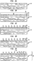
multilayer interconnection element 10 is shown inFig. 1 , havingdielectric portions 12 andconductive portions 14. The conductive portions may be in the form of wires, bond pads or the like. - The
multilayer interconnection element 10 may be formed of a single metal substrate or a multilayer substrate with dielectric such as polyimide, ceramic, FR4, BT resin and the like. Themultilayer interconnection element 10 may also be an interconnection element with multiple wiring layers or the like. Reference is also made toU.S. Pat. No. 6,528,784 which discusses the manufacture of a multilayer interconnection element, which is hereby incorporated by reference. - In one embodiment of the present invention, a
metallic layer 16 is laminated onto themultilayer interconnection element 10 using anadhesive 18 as illustrated inFig. 1B . Themetallic layer 16 may be any suitable metal as known in the art. For example, the metal may be any conductive metal, such as copper. Thereafter, themetallic layer 16 may be used to form microelectronic contacts orpins 20 as shown inFig. 1C . - The
microelectronic pins 20 may be formed as known in the art. For example, themicroelectronic pins 20 may be formed by photolithographically patterning a resist layer onmetallic layer 16 and transferring the resist patterns to themetallic layer 16 by etching. - Once the
microelectronic pins 20 are formed, where theadhesive layer 18 acts as an etch stop layer, theadhesive 18 may have portions removed from it to permit electrical connections to be formed between themicroelectronic pins 20 and theconductive portions 14 of themultilayer interconnection element 10, as shown inFig. 1D . Theadhesive 18 may be selectively removed using photolithographic techniques or the like, as known in the art. - Then, as shown in
Fig. 1E ,electrical connections 22 are formed adjacent the portions removed from theadhesive 18. For example, sputtering, also known as physical vapor deposition, or electroless plating may be followed by photolithographic patterning or laser drilling to define locations of the connections. Once theelectrical connections 22 have been formed, they may be electroplated to increase their thickness to an amount desired. This then results inelectrical connections 22 being formed between themultilayer interconnection element 10 and themicroelectronic pins 20. Lastly, a protective dielectric layer or film 24 (Fig. 1E ) may be deposited onto themultilayer interconnection element 10 covering theelectrical connections 22 and lower portions of themicroelectronic pins 20 to form theassembly 50 is not damaged. Thisprotective layer 24 can also assist in maintaining co-planarity of thetop surfaces 40 of themicroelectronic pins 20 because the dielectricprotective layer 24 reduces flexure when theassembly 50 is handled because it holds thepins 20 in a stiff fashion. Example protective layer materials include a solder mask or the like. - In another embodiment of the present invention, a
multilayer interconnection element 10 is illustrated as shown inFig. 2A . Thereafter, as shown inFig. 2B , a layeredmetallic structure 26 is joined to themultilayer interconnection element 10 using an adhesive 18. The layeredmetallic structure 26 may include a firstmetallic layer 28, anetch stop layer 30 and a secondmetallic layer 32. The firstmetallic layer 28, preferably, has a greater thickness than the secondmetallic layer 32. Although a trimetal structure is illustrated, the layeredmetallic structure 26 may include any number of layers. - Microelectronic pins 20 may be formed from the first
metallic layer 28, as shown inFig. 2C using techniques such as photolithographic patterning, or the like. However, the etch-stop layer remains. - A method of fabricating the
pins 20 will now be described with reference to the following figures. As shown inFIG. 3 , a plurality ofconductive pins 200 are formed to protrude above a surface of a continuousmetal wiring layer 210. Thepins 200 can be formed by a variety of different processes. Exemplary processes are described inU.S. Patent No. 6,884,709 , as well as in the U.S. Provisional Application entitled, "Chip Capacitor Embedded PWB" having serial number60/875,730 and a file date of January 11, 2007 - In one such process, an exposed metal layer of a multi-layer metal structure is etched in accordance with a photolithographically patterned photoresist layer to form
pins 200, the etching process stopping on aninterior metal layer 220 of the structure. Theinterior metal layer 220 includes one or more metals different from that of the exposed metal layer, theinterior metal layer 220 being of such composition that it is not attacked by the etchant used to etch the exposed metal layer.. For example, the metal layer from which thepins 200 are etched can consist essentially of copper, thecontinuous metal layer 210 can also consist essentially of copper, and theinterior metal layer 220 can consist essentially of nickel. Nickel provides good selectivity relative to copper to avoid the nickel layer from being attacked when the metal layer is etched to form pins 200. - After forming the
pins 200, a different etchant is then applied to remove the exposedinterior metal layer 220 by a process which is selective to theunderlying metal layer 210. Alternatively, another way that thepins 200 can be formed is by electroplating, in which pins are formed by plating a metal onto abase metal layer 210 through openings patterned in a dielectric layer such as a photoresist layer. - As indicated in plan view in
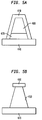
FIG. 4 , the pins can have a variety of different shapes and sizes. For example, when viewed from the top, the pins can have a shape which is circular 300, square or rectangular 310, oroval shape 320. When pins have a star shape, it may allow them to compress more easily or less easily than when other shapes are used. The height of thepins 200 above the plane of the underlying metal layer typically ranges between about 15 microns (pm) and about 250 microns (µm) and the width ranges for the tip of the pins is about 30 microns and above. -
FIGS. 5A and 5B illustrate exemplary alternative structures that the pins can take. For example, as illustrated inFIG. 5A , apin 400 is formed by etching a first metal layer selective to an etchstop metal layer 420 which overlies abase metal layer 440, thepin 400 being coated with asecond metal layer 410. The second metal layer can include the same metal as the first metal layer, one or more other metals, or a combination of a metal included in the first metal layer with another metal. In a particular embodiment, thesecond metal layer 410 includes a metal such as gold which is resistant to corrosion and which may also facilitate the formation of a diffusion bond between the second metal layer and a metal layer of another feature in contact therewith. In another particular embodiment, the second metal layer includes a low melting temperature metal such as tin or a low melting temperature metal alloy such as solder or a eutectic composition. Additional examples of one or more metals usable as a second metal layer include nickel, aluminum or nickel/gold. - As illustrated in
FIG. 5B , only the tip of aconductive pin 450 may be coated with asecond metal layer 460, and the body of the conductive pin may contact theadhesive layer 470 directly, without an intervening etch stop layer. - Thereafter, as shown in
Fig. 2D , portions of theetch stop layer 30, the secondmetallic layer 32 and the adhesive 18 may be removed. Theetch stop layer 30, the secondmetallic layer 32 and the adhesive 18 may be removed either simultaneously or sequentially, as desired. Removal of these layers permits electrically connecting themicroelectronic pins 20 with theconductive portions 14 of themultilayer interconnection element 10, as stated herein. Lastly, aprotective dielectric layer 24 such as described above (Fig. 1E ) may then be deposited atop the completed structure. - In yet another embodiment of the present invention, as illustrated in
Figs. 6A-6E a layeredmetallic structure 26 may be joined to amultilayer interconnection element 10 using an adhesive 18. However, prior to this step, the secondmetallic layer 32 has portions removed therefrom, such that when the layeredmetallic structure 26 is attached to themultilayer interconnection element 10 using the adhesive, some of the adhesive may then rise into the removed portions of the secondmetallic layer 32, as shown inFigs. 6B and 6C . Thus, the secondmetallic layer 32 may already be patterned prior to affixing the layeredmetallic structure 26 to themultilayer interconnection element 10. - Thereafter,
microelectronic pins 20 are formed in a manner as stated previously. Next, portions of theetch stop layer 30 and the adhesive 18 are removed as shown inFig. 6D . Then,electrical connections 22 are formed which electrically connect themicroelectronic pins 20 with theconductive portions 14 of themultilayer interconnection element 10. Lastly, aprotective layer 24 may be deposited to form theassembly 50. - The methods and structures described herein are advantageous for flip-chip mounting of a chip, having a land grid array ("LGA") or ball grid array ("BGA"), to the exposed pin interface such as that shown in
Fig. 7A . A chip may also be mounted to theassembly 50 on a side opposite themicroelectronic pins 20, as shown inFig. 7B . Further, the methods and structures are also advantageous for flip chip or wire bond microcontacts as shown inFig. 7C . The finished assembly may be a circuit panel or may be a circuit panel joined to a chip. Further, the finished assembly may be meant for interconnection to another circuit panel or a chip. - Although the invention herein has been described with reference to particular embodiments, it is to be understood that these embodiments are merely illustrative of the principles and applications of the present invention. It is therefore to be understood that numerous modifications may be made to the illustrative embodiments and that other arrangements may be devised without departing from the scope of the present invention as defined by the appended claims.
Claims (10)
- A method of forming contacts for an interconnection element, comprising:(a) joining a conductive element (16) to an interconnection element (10) having multiple wiring layers with a dielectric layer (18) between the conductive element and the interconnection element;(b) patterning the conductive element (16) to form conductive pins (20) such that at least a portion of a major surface of the dielectric layer (18) is exposed between at least some of the pins;(c) then forming openings in the dielectric layer (18) extending from the exposed portions of the major surface; and(d) then electrically interconnecting the conductive pins (20) with conductive features of the interconnection element (10) through the openings in the dielectric layer (18).
- The method of claim 1, wherein
step (a) includes joining the conductive element (16) to the interconnection element (10) with the dielectric layer (18), optionally
the dielectric layer includes an adhesive. - The method of claim 1 or 2, wherein step (c) includes forming electrically conductive traces extending within the openings in the dielectric layer (18), the traces interconnecting the conductive features with the conductive pins (20) .
- The method of claim 1, 2 or 3, wherein the conductive element (10) includes a single metal sheet.
- The method of claim 1, wherein the conductive element includes a layered metal structure (26, 30, 32).
- The method of claim 3, wherein the layered metal structure includes an outer metal layer (26), an inner metal layer (32) facing the interconnection element and a third metal layer (30) between the inner and outer metal layers, step (b) further includes etching the outer metal layer (26) selectively with respect to the third metal layer (30), and step (c) includes interconnecting the conductive features with portions of the inner metal layer (32).
- The method of claim 6, wherein
step (c) further includes forming openings in the third metal layer (30) and inner metal layer (32), the openings being aligned with the conductive features. - The method of claim 6 or 7, wherein the inner metal layer (32) has first openings and step (c) further includes forming through openings in the third metal layer (30), the through openings being aligned with the first openings and the conductive features.
- A method of forming a packaged chip including the method of forming contacts for an interconnection element as claimed in any preceding claim, further comprising:(d) electrically interconnecting contacts of a microelectronic element with the conductive pins (20).
- A method of forming a packaged chip including the method of forming contacts for an interconnection element as claimed in any of claims 1 to 7, wherein the conductive pins project from a first face of the interconnection element (10), the method further comprising:(d) electrically interconnecting contacts of a microelectronic element with second conductive features of the interconnection element (10) exposed at a second face of the interconnection element, the second face being remote from the first face.
Applications Claiming Priority (2)
| Application Number | Priority Date | Filing Date | Title |
|---|---|---|---|
| US11/824,484 US7911805B2 (en) | 2007-06-29 | 2007-06-29 | Multilayer wiring element having pin interface |
| PCT/US2008/007978 WO2009005696A1 (en) | 2007-06-29 | 2008-06-23 | Multilayer wiring element having pin interface |
Publications (3)
| Publication Number | Publication Date |
|---|---|
| EP2172089A1 EP2172089A1 (en) | 2010-04-07 |
| EP2172089A4 EP2172089A4 (en) | 2011-08-10 |
| EP2172089B1 true EP2172089B1 (en) | 2019-08-28 |
Family
ID=40160169
Family Applications (1)
| Application Number | Title | Priority Date | Filing Date |
|---|---|---|---|
| EP08779797.3A Active EP2172089B1 (en) | 2007-06-29 | 2008-06-23 | Method for manufacturing a multilayer wiring element having pin interface |
Country Status (6)
| Country | Link |
|---|---|
| US (1) | US7911805B2 (en) |
| EP (1) | EP2172089B1 (en) |
| JP (2) | JP5421254B2 (en) |
| KR (1) | KR101530896B1 (en) |
| CN (1) | CN101772995B (en) |
| WO (1) | WO2009005696A1 (en) |
Families Citing this family (55)
| Publication number | Priority date | Publication date | Assignee | Title |
|---|---|---|---|---|
| US8641913B2 (en) | 2003-10-06 | 2014-02-04 | Tessera, Inc. | Fine pitch microcontacts and method for forming thereof |
| US7495179B2 (en) | 2003-10-06 | 2009-02-24 | Tessera, Inc. | Components with posts and pads |
| US7709968B2 (en) | 2003-12-30 | 2010-05-04 | Tessera, Inc. | Micro pin grid array with pin motion isolation |
| US8525314B2 (en) | 2004-11-03 | 2013-09-03 | Tessera, Inc. | Stacked packaging improvements |
| US8058101B2 (en) | 2005-12-23 | 2011-11-15 | Tessera, Inc. | Microelectronic packages and methods therefor |
| US7911805B2 (en) * | 2007-06-29 | 2011-03-22 | Tessera, Inc. | Multilayer wiring element having pin interface |
| US8238114B2 (en) * | 2007-09-20 | 2012-08-07 | Ibiden Co., Ltd. | Printed wiring board and method for manufacturing same |
| KR101388538B1 (en) | 2007-09-28 | 2014-04-23 | 테세라, 인코포레이티드 | Flip chip interconnection with double post |
| US20100044860A1 (en) * | 2008-08-21 | 2010-02-25 | Tessera Interconnect Materials, Inc. | Microelectronic substrate or element having conductive pads and metal posts joined thereto using bond layer |
| US20100090339A1 (en) * | 2008-09-12 | 2010-04-15 | Kumar Ananda H | Structures and Methods for Wafer Packages, and Probes |
| US8330272B2 (en) | 2010-07-08 | 2012-12-11 | Tessera, Inc. | Microelectronic packages with dual or multiple-etched flip-chip connectors |
| US9159708B2 (en) | 2010-07-19 | 2015-10-13 | Tessera, Inc. | Stackable molded microelectronic packages with area array unit connectors |
| US8482111B2 (en) | 2010-07-19 | 2013-07-09 | Tessera, Inc. | Stackable molded microelectronic packages |
| US8580607B2 (en) | 2010-07-27 | 2013-11-12 | Tessera, Inc. | Microelectronic packages with nanoparticle joining |
| US8853558B2 (en) | 2010-12-10 | 2014-10-07 | Tessera, Inc. | Interconnect structure |
| JP5798435B2 (en) | 2011-03-07 | 2015-10-21 | 日本特殊陶業株式会社 | Wiring board for electronic component inspection apparatus and manufacturing method thereof |
| JP5777997B2 (en) * | 2011-03-07 | 2015-09-16 | 日本特殊陶業株式会社 | Wiring board for electronic component inspection apparatus and manufacturing method thereof |
| KR101128063B1 (en) | 2011-05-03 | 2012-04-23 | 테세라, 인코포레이티드 | Package-on-package assembly with wire bonds to encapsulation surface |
| US8404520B1 (en) | 2011-10-17 | 2013-03-26 | Invensas Corporation | Package-on-package assembly with wire bond vias |
| US8946757B2 (en) | 2012-02-17 | 2015-02-03 | Invensas Corporation | Heat spreading substrate with embedded interconnects |
| US8372741B1 (en) | 2012-02-24 | 2013-02-12 | Invensas Corporation | Method for package-on-package assembly with wire bonds to encapsulation surface |
| US8835228B2 (en) | 2012-05-22 | 2014-09-16 | Invensas Corporation | Substrate-less stackable package with wire-bond interconnect |
| US9391008B2 (en) | 2012-07-31 | 2016-07-12 | Invensas Corporation | Reconstituted wafer-level package DRAM |
| US9502390B2 (en) | 2012-08-03 | 2016-11-22 | Invensas Corporation | BVA interposer |
| US8878353B2 (en) | 2012-12-20 | 2014-11-04 | Invensas Corporation | Structure for microelectronic packaging with bond elements to encapsulation surface |
| US9136254B2 (en) | 2013-02-01 | 2015-09-15 | Invensas Corporation | Microelectronic package having wire bond vias and stiffening layer |
| US9167710B2 (en) | 2013-08-07 | 2015-10-20 | Invensas Corporation | Embedded packaging with preformed vias |
| US9685365B2 (en) | 2013-08-08 | 2017-06-20 | Invensas Corporation | Method of forming a wire bond having a free end |
| US20150076714A1 (en) | 2013-09-16 | 2015-03-19 | Invensas Corporation | Microelectronic element with bond elements to encapsulation surface |
| US9583456B2 (en) | 2013-11-22 | 2017-02-28 | Invensas Corporation | Multiple bond via arrays of different wire heights on a same substrate |
| US9379074B2 (en) | 2013-11-22 | 2016-06-28 | Invensas Corporation | Die stacks with one or more bond via arrays of wire bond wires and with one or more arrays of bump interconnects |
| US9263394B2 (en) | 2013-11-22 | 2016-02-16 | Invensas Corporation | Multiple bond via arrays of different wire heights on a same substrate |
| JP2014045221A (en) * | 2013-12-09 | 2014-03-13 | Sumitomo Electric Printed Circuit Inc | Manufacturing method of flexible printed wiring board sheet |
| US9583411B2 (en) | 2014-01-17 | 2017-02-28 | Invensas Corporation | Fine pitch BVA using reconstituted wafer with area array accessible for testing |
| US10381326B2 (en) | 2014-05-28 | 2019-08-13 | Invensas Corporation | Structure and method for integrated circuits packaging with increased density |
| US9735084B2 (en) | 2014-12-11 | 2017-08-15 | Invensas Corporation | Bond via array for thermal conductivity |
| US9888579B2 (en) | 2015-03-05 | 2018-02-06 | Invensas Corporation | Pressing of wire bond wire tips to provide bent-over tips |
| US9502372B1 (en) | 2015-04-30 | 2016-11-22 | Invensas Corporation | Wafer-level packaging using wire bond wires in place of a redistribution layer |
| US9761554B2 (en) | 2015-05-07 | 2017-09-12 | Invensas Corporation | Ball bonding metal wire bond wires to metal pads |
| KR101672640B1 (en) * | 2015-06-23 | 2016-11-03 | 앰코 테크놀로지 코리아 주식회사 | Semiconductor device |
| US9633971B2 (en) | 2015-07-10 | 2017-04-25 | Invensas Corporation | Structures and methods for low temperature bonding using nanoparticles |
| US10886250B2 (en) | 2015-07-10 | 2021-01-05 | Invensas Corporation | Structures and methods for low temperature bonding using nanoparticles |
| US10490528B2 (en) | 2015-10-12 | 2019-11-26 | Invensas Corporation | Embedded wire bond wires |
| US9490222B1 (en) | 2015-10-12 | 2016-11-08 | Invensas Corporation | Wire bond wires for interference shielding |
| US10332854B2 (en) | 2015-10-23 | 2019-06-25 | Invensas Corporation | Anchoring structure of fine pitch bva |
| US10181457B2 (en) | 2015-10-26 | 2019-01-15 | Invensas Corporation | Microelectronic package for wafer-level chip scale packaging with fan-out |
| US10043779B2 (en) | 2015-11-17 | 2018-08-07 | Invensas Corporation | Packaged microelectronic device for a package-on-package device |
| US9659848B1 (en) | 2015-11-18 | 2017-05-23 | Invensas Corporation | Stiffened wires for offset BVA |
| US9984992B2 (en) | 2015-12-30 | 2018-05-29 | Invensas Corporation | Embedded wire bond wires for vertical integration with separate surface mount and wire bond mounting surfaces |
| US9935075B2 (en) | 2016-07-29 | 2018-04-03 | Invensas Corporation | Wire bonding method and apparatus for electromagnetic interference shielding |
| US10299368B2 (en) | 2016-12-21 | 2019-05-21 | Invensas Corporation | Surface integrated waveguides and circuit structures therefor |
| US11225563B2 (en) | 2017-02-16 | 2022-01-18 | Azotek Co., Ltd. | Circuit board structure and composite for forming insulating substrates |
| US10743423B2 (en) | 2017-09-15 | 2020-08-11 | Azotek Co., Ltd. | Manufacturing method of composite substrate |
| US10813213B2 (en) | 2017-02-16 | 2020-10-20 | Azotek Co., Ltd. | High-frequency composite substrate and insulating structure thereof |
| US11044802B2 (en) | 2017-02-16 | 2021-06-22 | Azotek Co., Ltd. | Circuit board |
Family Cites Families (16)
| Publication number | Priority date | Publication date | Assignee | Title |
|---|---|---|---|---|
| JPS59178752A (en) | 1983-03-30 | 1984-10-11 | Hitachi Ltd | Multilayer interconnection substrate |
| JPS59198747A (en) | 1983-04-26 | 1984-11-10 | Nec Corp | Substrate with high density multilayer interconnection |
| JPH01308057A (en) | 1988-06-07 | 1989-12-12 | Matsushita Electric Ind Co Ltd | Multichip package |
| JP3925752B2 (en) * | 1997-08-08 | 2007-06-06 | 日立化成工業株式会社 | Bumped wiring board and manufacturing method of semiconductor package |
| JPH11298144A (en) * | 1998-04-15 | 1999-10-29 | Sanwa New Multi Kk | Manufacture of multilayered printed wiring board |
| JP3973340B2 (en) * | 1999-10-05 | 2007-09-12 | Necエレクトロニクス株式会社 | Semiconductor device, wiring board, and manufacturing method thereof |
| JP3653452B2 (en) * | 2000-07-31 | 2005-05-25 | 株式会社ノース | WIRING CIRCUIT BOARD, ITS MANUFACTURING METHOD, SEMICONDUCTOR INTEGRATED CIRCUIT DEVICE, AND ITS MANUFACTURING METHOD |
| US6586684B2 (en) * | 2001-06-29 | 2003-07-01 | Intel Corporation | Circuit housing clamp and method of manufacture therefor |
| WO2003083543A1 (en) * | 2002-04-01 | 2003-10-09 | Ibiden Co., Ltd. | Ic chip mounting substrate, ic chip mounting substrate manufacturing method, optical communication device, and optical communication device manufacturing method |
| JP3835352B2 (en) * | 2002-06-03 | 2006-10-18 | 株式会社デンソー | Bump forming method and bonding method of substrate having bump and other substrate |
| KR100455890B1 (en) * | 2002-12-24 | 2004-11-06 | 삼성전기주식회사 | A printed circuit board with embedded capacitors, and a manufacturing process thereof |
| JP2004327945A (en) * | 2003-04-30 | 2004-11-18 | Ngk Spark Plug Co Ltd | Ceramic electronic circuit component |
| FR2879347A1 (en) * | 2004-12-14 | 2006-06-16 | Commissariat Energie Atomique | ELECTRONIC DEVICE COMPRISING TWO COMPONENTS AND METHOD FOR MANUFACTURING SUCH A DEVICE |
| FR2879747A1 (en) | 2004-12-16 | 2006-06-23 | Oreal | In vitro evaluation of e.g. photoimmunosuppression/ photosensitization of a product, comprises applying the product on keratinocytes and Langerhan cells, evaluating the modulating capacity, analyzing and measuring gene expression rate |
| US7317249B2 (en) * | 2004-12-23 | 2008-01-08 | Tessera, Inc. | Microelectronic package having stacked semiconductor devices and a process for its fabrication |
| US7911805B2 (en) * | 2007-06-29 | 2011-03-22 | Tessera, Inc. | Multilayer wiring element having pin interface |
-
2007
- 2007-06-29 US US11/824,484 patent/US7911805B2/en active Active
-
2008
- 2008-06-23 EP EP08779797.3A patent/EP2172089B1/en active Active
- 2008-06-23 CN CN200880101950.6A patent/CN101772995B/en active Active
- 2008-06-23 KR KR1020107001200A patent/KR101530896B1/en active IP Right Grant
- 2008-06-23 JP JP2010514821A patent/JP5421254B2/en active Active
- 2008-06-23 WO PCT/US2008/007978 patent/WO2009005696A1/en active Application Filing
-
2013
- 2013-11-19 JP JP2013238596A patent/JP6001524B2/en active Active
Non-Patent Citations (1)
| Title |
|---|
| None * |
Also Published As
| Publication number | Publication date |
|---|---|
| CN101772995B (en) | 2016-07-13 |
| CN101772995A (en) | 2010-07-07 |
| EP2172089A1 (en) | 2010-04-07 |
| JP5421254B2 (en) | 2014-02-19 |
| US7911805B2 (en) | 2011-03-22 |
| US20090002964A1 (en) | 2009-01-01 |
| WO2009005696A1 (en) | 2009-01-08 |
| JP2014060431A (en) | 2014-04-03 |
| EP2172089A4 (en) | 2011-08-10 |
| KR101530896B1 (en) | 2015-06-23 |
| JP2010532567A (en) | 2010-10-07 |
| KR20100050457A (en) | 2010-05-13 |
| JP6001524B2 (en) | 2016-10-05 |
Similar Documents
| Publication | Publication Date | Title |
|---|---|---|
| EP2172089B1 (en) | Method for manufacturing a multilayer wiring element having pin interface | |
| KR101572600B1 (en) | Robust multi-layer wiring elements and assemblies with embedded microelectronic elements | |
| KR100603799B1 (en) | Metal foil having bumps, circuit substrate having the metal foil, and semiconductor device having the circuit substrate | |
| US7435680B2 (en) | Method of manufacturing a circuit substrate and method of manufacturing an electronic parts packaging structure | |
| US7122901B2 (en) | Semiconductor device | |
| US6297553B1 (en) | Semiconductor device and process for producing the same | |
| JP5224845B2 (en) | Semiconductor device manufacturing method and semiconductor device | |
| US7640655B2 (en) | Electronic component embedded board and its manufacturing method | |
| US8900464B2 (en) | Method of making a microelectronic interconnect element with decreased conductor spacing | |
| KR20070059186A (en) | Structure and method of making interconnect element, and multilayer wiring board including the interconnect element | |
| JPH10335528A (en) | Semiconductor package and manufacture thereof | |
| US6913814B2 (en) | Lamination process and structure of high layout density substrate | |
| JP2009004813A (en) | Wiring substrate for mounting semiconductor | |
| CN108305864B (en) | Terminal with a terminal body | |
| TWI624924B (en) | Wiring board with embedded component and integrated stiffener and method of making the same | |
| US9673063B2 (en) | Terminations | |
| JP2008529283A (en) | Composition and method for making interconnect elements having metal traces embedded in the surface of a dielectric | |
| TWI420996B (en) | Printed circuit board and method of manufacturing the same | |
| KR101543031B1 (en) | Printed circuit board and method for manufacturing the same | |
| JP2000058705A (en) | Semiconductor device and its manufacture | |
| KR101526581B1 (en) | Printed circuit board and method for manufacturing the same | |
| TW201828396A (en) | New terminal which can achieve low-cost, high-yield and more reliable interposer and multi-layer support structure | |
| JPH09275271A (en) | Printed-wiring board, manufacture thereof and printed circuit board |
Legal Events
| Date | Code | Title | Description |
|---|---|---|---|
| PUAI | Public reference made under article 153(3) epc to a published international application that has entered the european phase |
Free format text: ORIGINAL CODE: 0009012 |
|
| 17P | Request for examination filed |
Effective date: 20100128 |
|
| AK | Designated contracting states |
Kind code of ref document: A1 Designated state(s): AT BE BG CH CY CZ DE DK EE ES FI FR GB GR HR HU IE IS IT LI LT LU LV MC MT NL NO PL PT RO SE SI SK TR |
|
| AX | Request for extension of the european patent |
Extension state: AL BA MK RS |
|
| DAX | Request for extension of the european patent (deleted) | ||
| A4 | Supplementary search report drawn up and despatched |
Effective date: 20110707 |
|
| RIC1 | Information provided on ipc code assigned before grant |
Ipc: H05K 3/46 20060101AFI20110701BHEP |
|
| 17Q | First examination report despatched |
Effective date: 20140313 |
|
| GRAP | Despatch of communication of intention to grant a patent |
Free format text: ORIGINAL CODE: EPIDOSNIGR1 |
|
| STAA | Information on the status of an ep patent application or granted ep patent |
Free format text: STATUS: GRANT OF PATENT IS INTENDED |
|
| INTG | Intention to grant announced |
Effective date: 20190322 |
|
| GRAS | Grant fee paid |
Free format text: ORIGINAL CODE: EPIDOSNIGR3 |
|
| GRAA | (expected) grant |
Free format text: ORIGINAL CODE: 0009210 |
|
| STAA | Information on the status of an ep patent application or granted ep patent |
Free format text: STATUS: THE PATENT HAS BEEN GRANTED |
|
| AK | Designated contracting states |
Kind code of ref document: B1 Designated state(s): AT BE BG CH CY CZ DE DK EE ES FI FR GB GR HR HU IE IS IT LI LT LU LV MC MT NL NO PL PT RO SE SI SK TR |
|
| REG | Reference to a national code |
Ref country code: GB Ref legal event code: FG4D |
|
| REG | Reference to a national code |
Ref country code: CH Ref legal event code: EP |
|
| REG | Reference to a national code |
Ref country code: DE Ref legal event code: R096 Ref document number: 602008061035 Country of ref document: DE |
|
| REG | Reference to a national code |
Ref country code: AT Ref legal event code: REF Ref document number: 1174059 Country of ref document: AT Kind code of ref document: T Effective date: 20190915 |
|
| REG | Reference to a national code |
Ref country code: IE Ref legal event code: FG4D |
|
| REG | Reference to a national code |
Ref country code: NL Ref legal event code: FP |
|
| REG | Reference to a national code |
Ref country code: LT Ref legal event code: MG4D |
|
| PG25 | Lapsed in a contracting state [announced via postgrant information from national office to epo] |
Ref country code: FI Free format text: LAPSE BECAUSE OF FAILURE TO SUBMIT A TRANSLATION OF THE DESCRIPTION OR TO PAY THE FEE WITHIN THE PRESCRIBED TIME-LIMIT Effective date: 20190828 Ref country code: HR Free format text: LAPSE BECAUSE OF FAILURE TO SUBMIT A TRANSLATION OF THE DESCRIPTION OR TO PAY THE FEE WITHIN THE PRESCRIBED TIME-LIMIT Effective date: 20190828 Ref country code: SE Free format text: LAPSE BECAUSE OF FAILURE TO SUBMIT A TRANSLATION OF THE DESCRIPTION OR TO PAY THE FEE WITHIN THE PRESCRIBED TIME-LIMIT Effective date: 20190828 Ref country code: BG Free format text: LAPSE BECAUSE OF FAILURE TO SUBMIT A TRANSLATION OF THE DESCRIPTION OR TO PAY THE FEE WITHIN THE PRESCRIBED TIME-LIMIT Effective date: 20191128 Ref country code: NO Free format text: LAPSE BECAUSE OF FAILURE TO SUBMIT A TRANSLATION OF THE DESCRIPTION OR TO PAY THE FEE WITHIN THE PRESCRIBED TIME-LIMIT Effective date: 20191128 Ref country code: PT Free format text: LAPSE BECAUSE OF FAILURE TO SUBMIT A TRANSLATION OF THE DESCRIPTION OR TO PAY THE FEE WITHIN THE PRESCRIBED TIME-LIMIT Effective date: 20191230 Ref country code: LT Free format text: LAPSE BECAUSE OF FAILURE TO SUBMIT A TRANSLATION OF THE DESCRIPTION OR TO PAY THE FEE WITHIN THE PRESCRIBED TIME-LIMIT Effective date: 20190828 |
|
| PG25 | Lapsed in a contracting state [announced via postgrant information from national office to epo] |
Ref country code: LV Free format text: LAPSE BECAUSE OF FAILURE TO SUBMIT A TRANSLATION OF THE DESCRIPTION OR TO PAY THE FEE WITHIN THE PRESCRIBED TIME-LIMIT Effective date: 20190828 Ref country code: ES Free format text: LAPSE BECAUSE OF FAILURE TO SUBMIT A TRANSLATION OF THE DESCRIPTION OR TO PAY THE FEE WITHIN THE PRESCRIBED TIME-LIMIT Effective date: 20190828 Ref country code: GR Free format text: LAPSE BECAUSE OF FAILURE TO SUBMIT A TRANSLATION OF THE DESCRIPTION OR TO PAY THE FEE WITHIN THE PRESCRIBED TIME-LIMIT Effective date: 20191129 Ref country code: IS Free format text: LAPSE BECAUSE OF FAILURE TO SUBMIT A TRANSLATION OF THE DESCRIPTION OR TO PAY THE FEE WITHIN THE PRESCRIBED TIME-LIMIT Effective date: 20191228 |
|
| REG | Reference to a national code |
Ref country code: AT Ref legal event code: MK05 Ref document number: 1174059 Country of ref document: AT Kind code of ref document: T Effective date: 20190828 |
|
| PG25 | Lapsed in a contracting state [announced via postgrant information from national office to epo] |
Ref country code: TR Free format text: LAPSE BECAUSE OF FAILURE TO SUBMIT A TRANSLATION OF THE DESCRIPTION OR TO PAY THE FEE WITHIN THE PRESCRIBED TIME-LIMIT Effective date: 20190828 |
|
| PG25 | Lapsed in a contracting state [announced via postgrant information from national office to epo] |
Ref country code: EE Free format text: LAPSE BECAUSE OF FAILURE TO SUBMIT A TRANSLATION OF THE DESCRIPTION OR TO PAY THE FEE WITHIN THE PRESCRIBED TIME-LIMIT Effective date: 20190828 Ref country code: RO Free format text: LAPSE BECAUSE OF FAILURE TO SUBMIT A TRANSLATION OF THE DESCRIPTION OR TO PAY THE FEE WITHIN THE PRESCRIBED TIME-LIMIT Effective date: 20190828 Ref country code: PL Free format text: LAPSE BECAUSE OF FAILURE TO SUBMIT A TRANSLATION OF THE DESCRIPTION OR TO PAY THE FEE WITHIN THE PRESCRIBED TIME-LIMIT Effective date: 20190828 Ref country code: DK Free format text: LAPSE BECAUSE OF FAILURE TO SUBMIT A TRANSLATION OF THE DESCRIPTION OR TO PAY THE FEE WITHIN THE PRESCRIBED TIME-LIMIT Effective date: 20190828 Ref country code: AT Free format text: LAPSE BECAUSE OF FAILURE TO SUBMIT A TRANSLATION OF THE DESCRIPTION OR TO PAY THE FEE WITHIN THE PRESCRIBED TIME-LIMIT Effective date: 20190828 Ref country code: IT Free format text: LAPSE BECAUSE OF FAILURE TO SUBMIT A TRANSLATION OF THE DESCRIPTION OR TO PAY THE FEE WITHIN THE PRESCRIBED TIME-LIMIT Effective date: 20190828 |
|
| PG25 | Lapsed in a contracting state [announced via postgrant information from national office to epo] |
Ref country code: SK Free format text: LAPSE BECAUSE OF FAILURE TO SUBMIT A TRANSLATION OF THE DESCRIPTION OR TO PAY THE FEE WITHIN THE PRESCRIBED TIME-LIMIT Effective date: 20190828 Ref country code: CZ Free format text: LAPSE BECAUSE OF FAILURE TO SUBMIT A TRANSLATION OF THE DESCRIPTION OR TO PAY THE FEE WITHIN THE PRESCRIBED TIME-LIMIT Effective date: 20190828 Ref country code: IS Free format text: LAPSE BECAUSE OF FAILURE TO SUBMIT A TRANSLATION OF THE DESCRIPTION OR TO PAY THE FEE WITHIN THE PRESCRIBED TIME-LIMIT Effective date: 20200224 |
|
| REG | Reference to a national code |
Ref country code: DE Ref legal event code: R097 Ref document number: 602008061035 Country of ref document: DE |
|
| PLBE | No opposition filed within time limit |
Free format text: ORIGINAL CODE: 0009261 |
|
| STAA | Information on the status of an ep patent application or granted ep patent |
Free format text: STATUS: NO OPPOSITION FILED WITHIN TIME LIMIT |
|
| PG2D | Information on lapse in contracting state deleted |
Ref country code: IS |
|
| 26N | No opposition filed |
Effective date: 20200603 |
|
| PG25 | Lapsed in a contracting state [announced via postgrant information from national office to epo] |
Ref country code: SI Free format text: LAPSE BECAUSE OF FAILURE TO SUBMIT A TRANSLATION OF THE DESCRIPTION OR TO PAY THE FEE WITHIN THE PRESCRIBED TIME-LIMIT Effective date: 20190828 |
|
| PG25 | Lapsed in a contracting state [announced via postgrant information from national office to epo] |
Ref country code: MC Free format text: LAPSE BECAUSE OF FAILURE TO SUBMIT A TRANSLATION OF THE DESCRIPTION OR TO PAY THE FEE WITHIN THE PRESCRIBED TIME-LIMIT Effective date: 20190828 |
|
| REG | Reference to a national code |
Ref country code: CH Ref legal event code: PL |
|
| GBPC | Gb: european patent ceased through non-payment of renewal fee |
Effective date: 20200623 |
|
| PG25 | Lapsed in a contracting state [announced via postgrant information from national office to epo] |
Ref country code: LU Free format text: LAPSE BECAUSE OF NON-PAYMENT OF DUE FEES Effective date: 20200623 |
|
| REG | Reference to a national code |
Ref country code: BE Ref legal event code: MM Effective date: 20200630 |
|
| PG25 | Lapsed in a contracting state [announced via postgrant information from national office to epo] |
Ref country code: LI Free format text: LAPSE BECAUSE OF NON-PAYMENT OF DUE FEES Effective date: 20200630 Ref country code: IE Free format text: LAPSE BECAUSE OF NON-PAYMENT OF DUE FEES Effective date: 20200623 Ref country code: CH Free format text: LAPSE BECAUSE OF NON-PAYMENT OF DUE FEES Effective date: 20200630 Ref country code: FR Free format text: LAPSE BECAUSE OF NON-PAYMENT OF DUE FEES Effective date: 20200630 Ref country code: GB Free format text: LAPSE BECAUSE OF NON-PAYMENT OF DUE FEES Effective date: 20200623 |
|
| PG25 | Lapsed in a contracting state [announced via postgrant information from national office to epo] |
Ref country code: BE Free format text: LAPSE BECAUSE OF NON-PAYMENT OF DUE FEES Effective date: 20200630 |
|
| REG | Reference to a national code |
Ref country code: DE Ref legal event code: R082 Ref document number: 602008061035 Country of ref document: DE Representative=s name: ZACCO LEGAL RECHTSANWALTSGESELLSCHAFT MBH, DE |
|
| PG25 | Lapsed in a contracting state [announced via postgrant information from national office to epo] |
Ref country code: MT Free format text: LAPSE BECAUSE OF FAILURE TO SUBMIT A TRANSLATION OF THE DESCRIPTION OR TO PAY THE FEE WITHIN THE PRESCRIBED TIME-LIMIT Effective date: 20190828 Ref country code: CY Free format text: LAPSE BECAUSE OF FAILURE TO SUBMIT A TRANSLATION OF THE DESCRIPTION OR TO PAY THE FEE WITHIN THE PRESCRIBED TIME-LIMIT Effective date: 20190828 |
|
| PGFP | Annual fee paid to national office [announced via postgrant information from national office to epo] |
Ref country code: NL Payment date: 20230626 Year of fee payment: 16 Ref country code: DE Payment date: 20230627 Year of fee payment: 16 |