JP3973340B2 - Semiconductor device, wiring board, and manufacturing method thereof - Google Patents
Semiconductor device, wiring board, and manufacturing method thereof Download PDFInfo
- Publication number
- JP3973340B2 JP3973340B2 JP2000057767A JP2000057767A JP3973340B2 JP 3973340 B2 JP3973340 B2 JP 3973340B2 JP 2000057767 A JP2000057767 A JP 2000057767A JP 2000057767 A JP2000057767 A JP 2000057767A JP 3973340 B2 JP3973340 B2 JP 3973340B2
- Authority
- JP
- Japan
- Prior art keywords
- external electrode
- electrode pad
- wiring layer
- layer
- opening
- Prior art date
- Legal status (The legal status is an assumption and is not a legal conclusion. Google has not performed a legal analysis and makes no representation as to the accuracy of the status listed.)
- Expired - Lifetime
Links
Images


Classifications
-
- H—ELECTRICITY
- H10—SEMICONDUCTOR DEVICES; ELECTRIC SOLID-STATE DEVICES NOT OTHERWISE PROVIDED FOR
- H10W—GENERIC PACKAGES, INTERCONNECTIONS, CONNECTORS OR OTHER CONSTRUCTIONAL DETAILS OF DEVICES COVERED BY CLASS H10
- H10W42/00—Arrangements for protection of devices
- H10W42/121—Arrangements for protection of devices protecting against mechanical damage
-
- H—ELECTRICITY
- H10—SEMICONDUCTOR DEVICES; ELECTRIC SOLID-STATE DEVICES NOT OTHERWISE PROVIDED FOR
- H10W—GENERIC PACKAGES, INTERCONNECTIONS, CONNECTORS OR OTHER CONSTRUCTIONAL DETAILS OF DEVICES COVERED BY CLASS H10
- H10W70/00—Package substrates; Interposers; Redistribution layers [RDL]
- H10W70/60—Insulating or insulated package substrates; Interposers; Redistribution layers
-
- H—ELECTRICITY
- H05—ELECTRIC TECHNIQUES NOT OTHERWISE PROVIDED FOR
- H05K—PRINTED CIRCUITS; CASINGS OR CONSTRUCTIONAL DETAILS OF ELECTRIC APPARATUS; MANUFACTURE OF ASSEMBLAGES OF ELECTRICAL COMPONENTS
- H05K3/00—Apparatus or processes for manufacturing printed circuits
- H05K3/46—Manufacturing multilayer circuits
- H05K3/4644—Manufacturing multilayer circuits by building the multilayer layer by layer, i.e. build-up multilayer circuits
- H05K3/467—Adding a circuit layer by thin film methods
-
- H—ELECTRICITY
- H05—ELECTRIC TECHNIQUES NOT OTHERWISE PROVIDED FOR
- H05K—PRINTED CIRCUITS; CASINGS OR CONSTRUCTIONAL DETAILS OF ELECTRIC APPARATUS; MANUFACTURE OF ASSEMBLAGES OF ELECTRICAL COMPONENTS
- H05K3/00—Apparatus or processes for manufacturing printed circuits
- H05K3/46—Manufacturing multilayer circuits
- H05K3/4644—Manufacturing multilayer circuits by building the multilayer layer by layer, i.e. build-up multilayer circuits
- H05K3/4682—Manufacture of core-less build-up multilayer circuits on a temporary carrier or on a metal foil
-
- H—ELECTRICITY
- H10—SEMICONDUCTOR DEVICES; ELECTRIC SOLID-STATE DEVICES NOT OTHERWISE PROVIDED FOR
- H10P—GENERIC PROCESSES OR APPARATUS FOR THE MANUFACTURE OR TREATMENT OF DEVICES COVERED BY CLASS H10
- H10P72/00—Handling or holding of wafers, substrates or devices during manufacture or treatment thereof
- H10P72/70—Handling or holding of wafers, substrates or devices during manufacture or treatment thereof for supporting or gripping
- H10P72/74—Handling or holding of wafers, substrates or devices during manufacture or treatment thereof for supporting or gripping using temporarily an auxiliary support
-
- H—ELECTRICITY
- H10—SEMICONDUCTOR DEVICES; ELECTRIC SOLID-STATE DEVICES NOT OTHERWISE PROVIDED FOR
- H10W—GENERIC PACKAGES, INTERCONNECTIONS, CONNECTORS OR OTHER CONSTRUCTIONAL DETAILS OF DEVICES COVERED BY CLASS H10
- H10W70/00—Package substrates; Interposers; Redistribution layers [RDL]
- H10W70/01—Manufacture or treatment
- H10W70/05—Manufacture or treatment of insulating or insulated package substrates, or of interposers, or of redistribution layers
- H10W70/095—Manufacture or treatment of insulating or insulated package substrates, or of interposers, or of redistribution layers of vias therein
-
- H—ELECTRICITY
- H10—SEMICONDUCTOR DEVICES; ELECTRIC SOLID-STATE DEVICES NOT OTHERWISE PROVIDED FOR
- H10W—GENERIC PACKAGES, INTERCONNECTIONS, CONNECTORS OR OTHER CONSTRUCTIONAL DETAILS OF DEVICES COVERED BY CLASS H10
- H10W70/00—Package substrates; Interposers; Redistribution layers [RDL]
- H10W70/60—Insulating or insulated package substrates; Interposers; Redistribution layers
- H10W70/62—Insulating or insulated package substrates; Interposers; Redistribution layers characterised by their interconnections
- H10W70/63—Vias, e.g. via plugs
- H10W70/635—Through-vias
-
- H—ELECTRICITY
- H10—SEMICONDUCTOR DEVICES; ELECTRIC SOLID-STATE DEVICES NOT OTHERWISE PROVIDED FOR
- H10W—GENERIC PACKAGES, INTERCONNECTIONS, CONNECTORS OR OTHER CONSTRUCTIONAL DETAILS OF DEVICES COVERED BY CLASS H10
- H10W70/00—Package substrates; Interposers; Redistribution layers [RDL]
- H10W70/60—Insulating or insulated package substrates; Interposers; Redistribution layers
- H10W70/67—Insulating or insulated package substrates; Interposers; Redistribution layers characterised by their insulating layers or insulating parts
- H10W70/68—Shapes or dispositions thereof
- H10W70/685—Shapes or dispositions thereof comprising multiple insulating layers
-
- H—ELECTRICITY
- H10—SEMICONDUCTOR DEVICES; ELECTRIC SOLID-STATE DEVICES NOT OTHERWISE PROVIDED FOR
- H10W—GENERIC PACKAGES, INTERCONNECTIONS, CONNECTORS OR OTHER CONSTRUCTIONAL DETAILS OF DEVICES COVERED BY CLASS H10
- H10W74/00—Encapsulations, e.g. protective coatings
- H10W74/10—Encapsulations, e.g. protective coatings characterised by their shape or disposition
- H10W74/111—Encapsulations, e.g. protective coatings characterised by their shape or disposition the semiconductor body being completely enclosed
- H10W74/114—Encapsulations, e.g. protective coatings characterised by their shape or disposition the semiconductor body being completely enclosed by a substrate and the encapsulations
-
- H—ELECTRICITY
- H10—SEMICONDUCTOR DEVICES; ELECTRIC SOLID-STATE DEVICES NOT OTHERWISE PROVIDED FOR
- H10W—GENERIC PACKAGES, INTERCONNECTIONS, CONNECTORS OR OTHER CONSTRUCTIONAL DETAILS OF DEVICES COVERED BY CLASS H10
- H10W90/00—Package configurations
- H10W90/701—Package configurations characterised by the relative positions of pads or connectors relative to package parts
-
- H—ELECTRICITY
- H05—ELECTRIC TECHNIQUES NOT OTHERWISE PROVIDED FOR
- H05K—PRINTED CIRCUITS; CASINGS OR CONSTRUCTIONAL DETAILS OF ELECTRIC APPARATUS; MANUFACTURE OF ASSEMBLAGES OF ELECTRICAL COMPONENTS
- H05K3/00—Apparatus or processes for manufacturing printed circuits
- H05K3/10—Apparatus or processes for manufacturing printed circuits in which conductive material is applied to the insulating support in such a manner as to form the desired conductive pattern
- H05K3/20—Apparatus or processes for manufacturing printed circuits in which conductive material is applied to the insulating support in such a manner as to form the desired conductive pattern by affixing prefabricated conductor pattern
-
- H—ELECTRICITY
- H10—SEMICONDUCTOR DEVICES; ELECTRIC SOLID-STATE DEVICES NOT OTHERWISE PROVIDED FOR
- H10P—GENERIC PROCESSES OR APPARATUS FOR THE MANUFACTURE OR TREATMENT OF DEVICES COVERED BY CLASS H10
- H10P72/00—Handling or holding of wafers, substrates or devices during manufacture or treatment thereof
- H10P72/70—Handling or holding of wafers, substrates or devices during manufacture or treatment thereof for supporting or gripping
- H10P72/74—Handling or holding of wafers, substrates or devices during manufacture or treatment thereof for supporting or gripping using temporarily an auxiliary support
- H10P72/7424—Handling or holding of wafers, substrates or devices during manufacture or treatment thereof for supporting or gripping using temporarily an auxiliary support used as a support during the manufacture of self-supporting substrates
-
- H—ELECTRICITY
- H10—SEMICONDUCTOR DEVICES; ELECTRIC SOLID-STATE DEVICES NOT OTHERWISE PROVIDED FOR
- H10P—GENERIC PROCESSES OR APPARATUS FOR THE MANUFACTURE OR TREATMENT OF DEVICES COVERED BY CLASS H10
- H10P72/00—Handling or holding of wafers, substrates or devices during manufacture or treatment thereof
- H10P72/70—Handling or holding of wafers, substrates or devices during manufacture or treatment thereof for supporting or gripping
- H10P72/74—Handling or holding of wafers, substrates or devices during manufacture or treatment thereof for supporting or gripping using temporarily an auxiliary support
- H10P72/7438—Handling or holding of wafers, substrates or devices during manufacture or treatment thereof for supporting or gripping using temporarily an auxiliary support with parts of the auxiliary support remaining in the finished device
-
- H—ELECTRICITY
- H10—SEMICONDUCTOR DEVICES; ELECTRIC SOLID-STATE DEVICES NOT OTHERWISE PROVIDED FOR
- H10W—GENERIC PACKAGES, INTERCONNECTIONS, CONNECTORS OR OTHER CONSTRUCTIONAL DETAILS OF DEVICES COVERED BY CLASS H10
- H10W72/00—Interconnections or connectors in packages
- H10W72/01—Manufacture or treatment
- H10W72/0198—Manufacture or treatment batch processes
-
- H—ELECTRICITY
- H10—SEMICONDUCTOR DEVICES; ELECTRIC SOLID-STATE DEVICES NOT OTHERWISE PROVIDED FOR
- H10W—GENERIC PACKAGES, INTERCONNECTIONS, CONNECTORS OR OTHER CONSTRUCTIONAL DETAILS OF DEVICES COVERED BY CLASS H10
- H10W72/00—Interconnections or connectors in packages
- H10W72/071—Connecting or disconnecting
- H10W72/072—Connecting or disconnecting of bump connectors
- H10W72/07202—Connecting or disconnecting of bump connectors using auxiliary members
- H10W72/07204—Connecting or disconnecting of bump connectors using auxiliary members using temporary auxiliary members, e.g. sacrificial coatings
- H10W72/07207—Temporary substrates, e.g. removable substrates
-
- H—ELECTRICITY
- H10—SEMICONDUCTOR DEVICES; ELECTRIC SOLID-STATE DEVICES NOT OTHERWISE PROVIDED FOR
- H10W—GENERIC PACKAGES, INTERCONNECTIONS, CONNECTORS OR OTHER CONSTRUCTIONAL DETAILS OF DEVICES COVERED BY CLASS H10
- H10W72/00—Interconnections or connectors in packages
- H10W72/851—Dispositions of multiple connectors or interconnections
- H10W72/874—On different surfaces
- H10W72/877—Bump connectors and die-attach connectors
-
- H—ELECTRICITY
- H10—SEMICONDUCTOR DEVICES; ELECTRIC SOLID-STATE DEVICES NOT OTHERWISE PROVIDED FOR
- H10W—GENERIC PACKAGES, INTERCONNECTIONS, CONNECTORS OR OTHER CONSTRUCTIONAL DETAILS OF DEVICES COVERED BY CLASS H10
- H10W74/00—Encapsulations, e.g. protective coatings
- H10W74/10—Encapsulations, e.g. protective coatings characterised by their shape or disposition
- H10W74/131—Encapsulations, e.g. protective coatings characterised by their shape or disposition the semiconductor body being only partially enclosed
- H10W74/142—Encapsulations, e.g. protective coatings characterised by their shape or disposition the semiconductor body being only partially enclosed the encapsulations exposing the passive side of the semiconductor body
-
- H—ELECTRICITY
- H10—SEMICONDUCTOR DEVICES; ELECTRIC SOLID-STATE DEVICES NOT OTHERWISE PROVIDED FOR
- H10W—GENERIC PACKAGES, INTERCONNECTIONS, CONNECTORS OR OTHER CONSTRUCTIONAL DETAILS OF DEVICES COVERED BY CLASS H10
- H10W74/00—Encapsulations, e.g. protective coatings
- H10W74/10—Encapsulations, e.g. protective coatings characterised by their shape or disposition
- H10W74/15—Encapsulations, e.g. protective coatings characterised by their shape or disposition on active surfaces of flip-chip devices, e.g. underfills
-
- H—ELECTRICITY
- H10—SEMICONDUCTOR DEVICES; ELECTRIC SOLID-STATE DEVICES NOT OTHERWISE PROVIDED FOR
- H10W—GENERIC PACKAGES, INTERCONNECTIONS, CONNECTORS OR OTHER CONSTRUCTIONAL DETAILS OF DEVICES COVERED BY CLASS H10
- H10W90/00—Package configurations
- H10W90/701—Package configurations characterised by the relative positions of pads or connectors relative to package parts
- H10W90/721—Package configurations characterised by the relative positions of pads or connectors relative to package parts of bump connectors
- H10W90/724—Package configurations characterised by the relative positions of pads or connectors relative to package parts of bump connectors between a chip and a stacked insulating package substrate, interposer or RDL
-
- H—ELECTRICITY
- H10—SEMICONDUCTOR DEVICES; ELECTRIC SOLID-STATE DEVICES NOT OTHERWISE PROVIDED FOR
- H10W—GENERIC PACKAGES, INTERCONNECTIONS, CONNECTORS OR OTHER CONSTRUCTIONAL DETAILS OF DEVICES COVERED BY CLASS H10
- H10W90/00—Package configurations
- H10W90/701—Package configurations characterised by the relative positions of pads or connectors relative to package parts
- H10W90/731—Package configurations characterised by the relative positions of pads or connectors relative to package parts of die-attach connectors
- H10W90/734—Package configurations characterised by the relative positions of pads or connectors relative to package parts of die-attach connectors between a chip and a stacked insulating package substrate, interposer or RDL
-
- H—ELECTRICITY
- H10—SEMICONDUCTOR DEVICES; ELECTRIC SOLID-STATE DEVICES NOT OTHERWISE PROVIDED FOR
- H10W—GENERIC PACKAGES, INTERCONNECTIONS, CONNECTORS OR OTHER CONSTRUCTIONAL DETAILS OF DEVICES COVERED BY CLASS H10
- H10W90/00—Package configurations
- H10W90/701—Package configurations characterised by the relative positions of pads or connectors relative to package parts
- H10W90/731—Package configurations characterised by the relative positions of pads or connectors relative to package parts of die-attach connectors
- H10W90/736—Package configurations characterised by the relative positions of pads or connectors relative to package parts of die-attach connectors between a chip and a stacked lead frame, conducting package substrate or heat sink
-
- Y—GENERAL TAGGING OF NEW TECHNOLOGICAL DEVELOPMENTS; GENERAL TAGGING OF CROSS-SECTIONAL TECHNOLOGIES SPANNING OVER SEVERAL SECTIONS OF THE IPC; TECHNICAL SUBJECTS COVERED BY FORMER USPC CROSS-REFERENCE ART COLLECTIONS [XRACs] AND DIGESTS
- Y10—TECHNICAL SUBJECTS COVERED BY FORMER USPC
- Y10S—TECHNICAL SUBJECTS COVERED BY FORMER USPC CROSS-REFERENCE ART COLLECTIONS [XRACs] AND DIGESTS
- Y10S438/00—Semiconductor device manufacturing: process
- Y10S438/977—Thinning or removal of substrate
Landscapes
- Engineering & Computer Science (AREA)
- Manufacturing & Machinery (AREA)
- Microelectronics & Electronic Packaging (AREA)
- Internal Circuitry In Semiconductor Integrated Circuit Devices (AREA)
- Production Of Multi-Layered Print Wiring Board (AREA)
- Wire Bonding (AREA)
- Structures For Mounting Electric Components On Printed Circuit Boards (AREA)
Abstract
Description
【0001】
【発明の属する技術分野】
本発明は、配線基板、配線基板を有する半導体装置、及び、配線基板の製造方法、半導体装置の配線基板への実装方法に関し、特に、多層化された配線基板にフリップチップ型半導体チップが実装される配線基板、配線基板を有する半導体装置、及び、その製造方法、実装方法に関する。
【0002】
【従来の技術】
近年、高密度実装が可能な半導体装置として、フリップチップ型半導体装置の重要性が高まっている。図52に従来のフリップチップ型半導体装置を示す。フリップチップ型半導体チップ101は、その周辺部又は活性領域上に所定のエリアアレー配列で形成された外部端子(図示せず)と、その外部端子上に設けられ、半田、Au、Sn−Ag系合金等の金属性材料からなる突起状のバンプ102とを有する。
【0003】
図53に示すように、このフリップチップ型半導体チップ101は、バンプ配列パターンと同一パターンの電極パット(図示せず)を備えた多層配線基板103に実装される。通常、バンプ材料として半田を用いる場合には、Fluxを使用したIRリフロー工程により、フリップチップ型半導体チップ101を多層配線基板103に実装する。半導体チップ101が実装された多層配線基板103は、外部端子(図示せず)を介して、回路基板に実装される。
【0004】
このような実装方法では、多層配線基板とフリップチップ型半導体チップ101の線膨張係数の相違により、実装信頼性のうち特に温度サイクル特性が劣るという問題点がある。この問題点を解決するために、従来から以下に述べるような施策がとられている。
【0005】
まず、第1の方法は、多層配線基板として、半導体チップのシリコンとの線膨張係数の差が小さいAlN、ムライド、ガラセラ等のセラッミック系の材料を用いる方法である。この方法は、実装信頼性の向上という観点では効果があるが、多層配線基板の材料として高価なセラミック系材料を使用するため、適用範囲がHighエンドなスーパーコンピューターや、大型コンピューターの特定用途に限定される。
【0006】
第2の方法として、半導体チップのシリコンよりも線膨張係数は大きいが、比較的安価である有機系材料からなる多層配線基板を用いる方法がある。この方法では、半導体チップと多層配線基板との間にアンダーフィル樹脂を設ける。この結果、半導体チップと多層配線基板とを接続するバンプ部分に働くせん断応力を、バンプを覆うアンダーフィル樹脂に分散させ、実装信頼性を向上させることができる。
【0007】
第2の方法で用いる有機系材料を使用した多層配線基板としては、バンプ配列パターンの最小ピッチ及びピン数の関係上、通常ビルドアップ基板と呼ばれる多層配線基板が使用される。このビルドアップ基板の製造方法を、図54乃至図59に示す。
【0008】
まず、図54に示すように、FR4、FR5、BT基板等に代表される絶縁性のガラスエポキシ系基材104の両面に10〜40μmの所定の厚みのCu箔105を貼りつけ、パターニング処理する。次に、基板両面のCu箔層を電気的に接続するために、ドリル加工等で基板に穴あけをし、スルーホールメッキ処理を施して、貫通スルーホール部106を形成する。この貫通スルーホール部106には絶縁性のスルーホール穴埋め用樹脂を充填して、後工程のプロセス安定性及び基板の品質安定性を確保する。これをコア基板107とする。
【0009】
次に、図55に示すように、Cu配線パターン上に絶縁性樹脂108を形成し、フォトレジスト技術によるケミカルエッチング法又はレーザー加工技術等で所定の位置に絶縁性樹脂開口部109を形成する。
次に、図56に示すように、スパッタリング法又はCu無電解メッキ法等によりTi/Cu等の金属薄膜層110を形成する。続いて、図57に示すように、厚さ20〜40μm程度のフォトレジスト111又はドライフィルムを金属薄膜層110上に形成し、露光・現像処理でパターニングする。その後、図58に示すように、金属薄膜層110を給電層として電解Cuメッキ処理により配線パターン部112を形成する。次に、図59に示すように、フォトレジスト又はドライフィルムを剥離後、配線パターン部112をマスクとして、ウエットエッチング処理により金属薄膜層110を除去し、配線パターン部を電気的に独立させる。以上の図54乃至図59に示す工程を繰り返して、必要に応じて6層、8層の多層配線を有するビルドアップ基板を作成する。
【0010】
【発明が解決しようとする課題】
第2の方法で用いる多層配線基板は、比較的安価で、スルーホール形成の加工性に優れたガラスエポキシ系基材で形成するが、ガラスエポキシ系基材は半導体チップとの熱膨張係数の差が大きいので、両者間には応力が発生し、接続の信頼性が低下する。そこで、この応力の緩和を目的として、ガラスエポキシ系基材上に形成する配線パターンには10〜30μm程度の膜厚を持たせている。従って、配線のパターニング時にマスクとして用いるフォトレジスト又はドライフィルムは、20〜40μm程度の厚みが必要である。この結果、露光・現像工程のパターンピッチ及び配線パターンピッチは、最小でも30μm程度であり、多層配線基板の高密度化と基板外形の小型化とを図ることが出来ないという問題がある。
【0011】
この様に、従来の多層配線基板はガラスエポキシ系基材を使用するため、必要な再配線機能を持たせたまま多層配線基板の外形寸法を縮小することが出来ない。そのため、基材そのものは安価であるにも関わらず、一枚の大パネルから製造できる多層配線基板の枚数が少なく、多層配線基板のコストの低減が困難である。また、ガラスエポキシ基材では、多層配線層を構成する絶縁性樹脂108形成時の応力に起因するソリが発生する。更に、実装時の多層配線基板と回路基板との熱膨張率の差に起因する応力により、両者間の接続の信頼性が劣るという問題がある。
【0012】
本願発明は、金属板上に多層配線層を形成することで、これらの問題を解決するとともに、高信頼性の多層配線基板を提供することを目的とする。
【0013】
【課題を解決するための手段】
本発明の半導体装置の製造方法は、金属板上に選択的に外部電極パッドを形成する工程と、前記外部電極パッドに対応する位置に第1の開口を有する第1絶縁層を形成する工程と、前記第1の開口を介して前記外部電極パッドに電気的に接続する第1配線層を形成する工程と、前記第1配線層に対応する位置に第2の開口を有する第2絶縁層を形成する工程と、前記第2の開口を介して前記第1配線層と電気的に接続する第2配線層を形成する工程と、 前記金属板の前記第1絶縁層に接する部分を選択的にエッチング除去し、前記外部電極パッドに一端が接し前記外部電極パッドと電気的に接続する柱状の導電体を形成する工程と、 前記第2配線層に外部電極を介して接続する半導体チップを搭載する工程と、前記柱状の導電体間に絶縁性樹脂層を形成する工程と、前記柱状の導電体の他端に、回路基板と前記半導体チップの外部電極端子とを電気的に接続するための外部端子を形成する工程と、 前記絶縁性樹脂層上に、前記外部端子に対応する位置に開口を有する支持板を設け、前記絶縁性樹脂層表面と前記外部端子側面と前記支持板内周面とで囲まれた空間に接着樹脂を注入する工程とを有することを特徴とする。また、本発明の半導体装置の製造方法は、金属板上に直接に外部電極パッドを形成する工程と、 前記外部電極パッドに対応する位置に第1の開口を有する第1絶縁層を形成する工程と、前記第1の開口を介して前記外部電極パッドに電気的に接続する第1配線層を形成する工程と、前記第1配線層に対応する位置に第2の開口を有する第2絶縁層を形成する工程と、前記第2の開口を介して前記第1配線層と電気的に接続する第2配線層を形成する工程と、前記金属板を少なくとも前記外部電極パッドが露出するようにエッチング除去する工程と、前記金属板をエッチング除去する工程の後に、導電性接着剤を用いて柱状の導電体の一端を前記外部電極パッドに接続する工程と、前記第2配線層に外部電極端子を介して接続する半導体チップを搭載する工程と、前記柱状の導電体間に絶縁性樹脂層を形成する工程と、前記柱状の導電体の他端に、回路基板と前記半導体チップの外部電極端子とを電気的に接続するための外部端子を形成する工程と、前記絶縁性樹脂層上に、前記外部端子に対応する位置に開口を有する支持板を設け、前記絶縁性樹脂層表面と前記外部端子側面と前記支持板内周面とで囲まれた空間に接着樹脂を注入する工程とを有することを特徴とする。本発明の半導体装置の製造方法では、金属板上に多層配線層を形成する工程を有しており、製造中の熱処理等で配線層中に応力が発生しても、配線層は剛性の高い金属板に固着されているので反りが抑制され、微細なパターンを確実に形成できる。
【0014】
この様にして、半導体チップとの熱膨張係数の差の大きなガラスエポキシ基板を介さずに半導体チップを回路基板に実装できるので、半導体チップとガラスエポキシ基板間の応力緩衝を目的として配線パターンの膜厚を大きくする必要は無い。
【0015】
本発明の半導体装置は、外部電極パッドと、前記外部電極パッド上に設けられ、前記外部電極パッドの対応する位置に形成される第1の開口及び前記外部電極パッドの面と実質的に平坦である下面を有する第1絶縁層と、前記第1の開口を介して前記外部電極パッドと電気的に接続し前記第1絶縁層上に設けられた第1配線層と、前記第1配線層上に設けられ前記第1配線層の対応する位置に第2の開口を有する第2絶縁層と、前記第2の開口を介して前記第1配線層と電気的に接続する第2配線層と、一端が前記外部電極パッドに接合して電気的に接続され、前記外部電極パッド毎に独立して設けられた柱状の導電体と、により形成される配線基板と、前記第2配線層に外部電極端子を介して接続される半導体チップと、前記柱状の導電体の他端に、回路基板と前記半導体チップの外部電極端子とを電気的に接続するための外部端子と、を有し、前記柱状の導電体を複数有し、前記複数の導電体が絶縁性樹脂を介して互いに絶縁されているとともに、前記複数の柱状の導電体と前記絶縁性樹脂とで構成される基板層は、前記配線基板より高い剛性を有することを特徴とする。
また、本発明の半導体装置は、外部電極パッドと、前記外部電極パッドの上面に設けられ、前記外部電極パッドの対応する位置に形成される第1の開口及び前記外部電極パッドの面と実質的に平坦である下面を有する第1絶縁層と、前記第1の開口を介して前記外部電極パッドと電気的に接続し前記第1絶縁層上に設けられた第1配線層と、前記第1配線層上に設けられ前記第1配線層の対応する位置に第2の開口を有する第2絶縁層と、前記第2の開口を介して前記第1配線層と電気的に接続する第2配線層と、前記外部電極パッドに導電性接着剤で一端が電気的に接続され、前記外部電極パッド毎に独立して設けられた柱状の導電体と、により形成される配線基板と、前記第2配線層に外部電極端子を介して接続される半導体チップと、前記柱状の導電体の他端に、回路基板と前記半導体チップの外部電極端子とを電気的に接続するための外部端子と、を有し、前記柱状の導電体を複数有し、前記複数の導電体が絶縁性樹脂を介して互いに絶縁されているとともに、前記複数の柱状の導電体と前記絶縁性樹脂とで構成される基板層は、前記配線基板より高い剛性を有することを特徴とする。
また、本発明の半導体装置は、外部電極パッドと、前記外部電極パッドの上面に設けられ、前記外部電極パッドの対応する位置に形成される第1の開口及び前記外部電極パッドの面と実質的に平坦である下面を有する第1絶縁層と、前記第1の開口を介して前記外部電極パッドと電気的に接続し前記第1絶縁層上に設けられた第1配線層と、前記第1配線層上に設けられ前記第1配線層の対応する位置に第2の開口を有する第2絶縁層と、前記第2の開口を介して前記第1配線層と電気的に接続する第2配線層と、一端が前記外部電極パッドに接合して電気的に接続され、前記外部電極パッド毎に独立して設けられた柱状の導電体と、により形成される配線基板と、前記第2配線層に外部電極端子を介して接続される半導体チップと、前記柱状の導電体の他端に、回路基板と前記半導体チップの外部電極端子とを電気的に接続するための外部端子と、を有し、前記第1絶縁層の下面に接して前記柱状の導電体の側面と前記外部端子の側壁の一部を覆う接着樹脂を有することを特徴とする。
また、本発明の半導体装置は、外部電極パッドと、前記外部電極パッドの上面に設けられ、前記外部電極パッドの対応する位置に形成される第1の開口及び前記外部電極パッドの面と実質的に平坦である下面を有する第1絶縁層と、前記第1の開口を介して前記外部電極パッドと電気的に接続し前記第1絶縁層上に設けられた第1配線層と、前記第1配線層上に設けられ前記第1配線層の対応する位置に第2の開口を有する第2絶縁層と、前記第2の開口を介して前記第1配線層と電気的に接続する第2配線層と、前記外部電極パッドに導電性接着剤で一端が電気的に接続され、前記外部電極パッド毎に独立して設けられた柱状の導電体と、により形成される配線基板と、前記第2配線層に外部電極端子を介して接続される半導体チップと、前記柱状の導電体の他端に、回路基板と前記半導体チップの外部電極端子とを電気的に接続するための外部端子と、を有し、前記第1絶縁層の下面に接して前記柱状の導電体の側面と前記外部端子の側壁の一部を覆う接着樹脂を有すること を特徴とする。
【0016】
本発明の半導体装置は、一端が外部電極パッドに接続された柱状の導電体を備えており、この柱状の導電体は半導体装置と回路基板との間の応力を緩和する効果を有し、両者間の接続の信頼性を向上させることが出来る。
【0017】
【発明の実施の形態】
〔第1の実施の形態〕
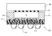
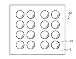
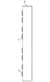
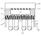
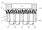
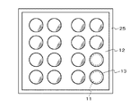
図1は、本発明によるフリップチップ型半導体装置の第1の実施の形態を示す。半導体チップ2が、多層配線層3で構成される多層配線基板にフリップ実装されている。図2は、図1に示す半導体装置32を半田ボール13側の底面から見た平面図である。
【0018】
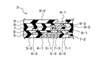
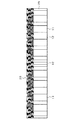
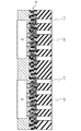
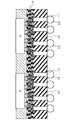
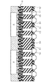
多層配線層3は、図3に示すように、第1配線層5、第2配線層6、第3配線層7、第4配線層8、第5配線層9とから形成されている。第2配線層6は第1配線層5の上面側に、第3配線層7は第2配線層6の上面側に、第4配線層8は第3配線層7の上面側に、第5配線層9は第4配線層8の上面側にそれぞれに形成されている。
【0019】
第1配線層5は、第1配線層配線部5−1と第1配線層絶縁層5−2と第1配線層接続層5−3とから形成されている。第2配線層6は、第2配線層配線部6−1と第2配線層絶縁層6−2と第2配線層接続層6−3とから形成されている。第3配線層7は、第3配線層配線部7−1と第3配線層絶縁層7−2と第3配線層接続層7−3とから形成されている。第4配線層8は、第4配線層配線部8−1と第4配線層絶縁層8−2と第4配線層接続層8−3とから形成されている。第5配線層9は、第1配線層配線部9−1と第5配線層絶縁層9−2(後述されるソルダーレジスト層)とから形成されている。複数の配線部は、複数の接続層を介してそれぞれに接続している。
【0020】
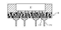
この多層配線層3には、その上面側に、フリップチップ型の半導体チップ2が電気的に接合されている。半導体チップ2は、その下面側に複数のバンプ電極14が形成されており、これらのバンプ電極14を介して、第1配線層配線部9−1に電気的に接合する。半導体チップ2と第5配線層9は、絶縁性樹脂被覆15により覆われて外界から保護されている。
【0021】
図4〜図20に、本実施の形態の半導体装置の製造方法を示す。図4に示すように、金属板16は、半導体ウエハー形状をしたCu板である。金属板16を使用する理由は、十分な剛性を有するからである。金属板16の材料としては、Cuの他に、Ni、Al、W,Mo、Au、Ag、Ptを主成分とする金属材料または異種金属の複合材料、セラミックスその他の高剛性材料が用いられ得る。
【0022】
次に、図5に示すように、金属板16の上面に、スパッタリング法等により接着金属層となるTi、Cr、Mo、W系合金の薄膜を形成した後、スパッタリング法等により電極材料となるCu、AL、又はNi等の薄膜を形成する。その後、フォトレジストの露光・現像処理、ウエットエッチング法、又は、プラズマ表面処理技術が流用されるドライエッチングにより、先に形成した薄膜をパターニングして外部電極パッド部17を形成する。尚、外部電極パッドピッチが狭ピッチでない場合には、金属板16にフォトレジストをコーティングして露光・現像処理を施した後、Cu、Ni等の材料を用いた電解メッキ処理により形成することも出来る。
【0023】
次に、図6に示すように、金属板16と外部電極パッド部17の上面に、絶縁性樹脂薄膜層18を形成する。絶縁性樹脂薄膜層18は、液状の絶縁性材料のスピンコーティング法、又は、プラズマ表面処理技術が流用されるCVD(Chemical Vapor Deposition)法、PVD(Physical Vapor Deposition)法により形成されるポリイミド系樹脂である。
【0024】
その他、絶縁性樹脂薄膜層18としては、ポリイミド系樹脂の他に、SiO2系無機材料、エポキシ系樹脂、シリコーン系樹脂、ポリオレフィン系樹脂、シアネートエステル系樹脂、フェノール系樹脂、ナフタレン系樹脂等の有機系材料のいずれかを主成分として構成することが出来る。特に、1.0μm以下の微細パターンを形成する場合には、半導体の拡散プロセスを採用できるSiO2系無機材料を使用することが好ましい。
【0025】
次に、図7に示すように、外部電極パッド部17上の絶縁性樹脂薄膜層18を部分的に除去し、絶縁性樹脂薄膜開口部19を形成する。まず、フォトレジストを外部電極パッド部17上にコーティングし、露光・現像処理を行う。次に、絶縁性樹脂薄膜層18がケミカルエッチング可能な物質で構成されているならばウエットエッチングを、又は、絶縁性樹脂薄膜層18がケミカルエッチング不可能な物質で構成されているならばプラズマ表面処理技術が流用されるドライエッチングを行い、絶縁性樹脂薄膜開口部19を形成する。
【0026】
次に、図8に示すように、外部電極パッド部17と絶縁性樹脂薄膜層18の上側の全面に、外部電極パッド部17に対する金属薄膜層21の接着金属層となるTi、Cr、Mo、W系合金の薄膜をスパッタリング法等により形成する。その後、この接着金属層の上面に電極材料となるCu、AL、又は、Ni等の薄膜をスパッタリング法・CVD法無電解メッキ法等により形成し、金属薄膜21とする。
【0027】
次に、フォトレジストをマスクとして、ウエットエッチング法、又は、プラズマ表面処理技術が流用されるドライエッチング技術により、金属薄膜21をパターニングして図9に示す金属薄膜配線部22を形成する。外部電極パッド部17は、図3に示される第1配線層配線部5−1に相当し、金属薄膜配線部22は図3に示される第2配線層6の第2配線層配線部6−1と第1配線層接続層5−3とに相当する。尚、金属薄膜配線部22のパターンピッチが粗い場合等には、金属薄膜層21を形成後に、フォトレジストで金属薄膜配線パターンを形成し、Cu等の電解メッキ処理により配線パターンを形成してもよい。上記配線パターンの形成においては、フォトレジストの厚み及び金属薄膜配線部は、1μm以下とすることができる。
【0028】
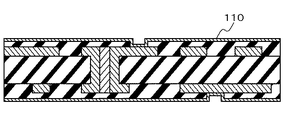
次に、フォトレジストの剥離と、配線パターンをマスクとする金属薄膜層のエッチング処理とを行い、金属薄膜配線部22を形成する。引き続き、図10〜図14に示すように、絶縁性樹脂薄膜層18の形成から金属薄膜配線部22の形成までの工程を所定のそれぞれのパターンにより繰返し、所定の多層配線構造を形成し、図3に示す多層配線層3の第4配線層8までを形成する。
【0029】
次に、図15に示すように、金属薄膜配線形成技術により、第4配線層8の上層であって、フリップチップ型半導体チップのバンプ電極パターンに対応する位置に、パッド電極部23を形成する。パッド電極部23は、第5配線層9の第1配線層配線部9−1に相当する。
【0030】
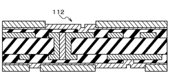
その後、パッド電極部23を含む多層配線層3を保護するために、図16に示すソルダーレジスト膜24を形成する。ソルダーレジスト膜24は、既述の通り、第5配線層絶縁層9−2に相当し、パッド電極部23に対応する位置に開口部24a(ソルダーレジスト膜24に設けられる開口、第2の開口)が設けられている。この開口部は、ソルダーレジスト膜24が非感光性材料で形成されている場合は、フォトレジストをマスクとして、ウエットエッチング法又はプラズマ表面処理技術が流用されるドライエッチングを行い形成する。また、ソルダーレジスト膜24が感光性材料で形成されている場合は、そのまま露光・現像処理を行い形成する。
【0031】
ソルダーレジスト膜としては、エポキシ系樹脂に酸化シリコンの微細粉末等の無機フィラー等を入れた有機系絶縁性材料を使用する。その他にも、外部からの機械的応力に強く、Flux洗浄液やAuメッキ液に対する耐性が大きく、アンダーフィル材等の封止材料との密着特性が優れた材料を選択することが出来る。
尚、多層配線構造中の絶縁性樹脂薄膜層18が機械的応力と化学的応力に関して高い信頼性を有する場合には、ソルダーレジスト膜24の形成は省略できる。
【0032】
これらの工程の後、図17に示すように、金属板16を全てエッチング除去する。
【0033】
次に、多層配線構造の最下層である外部電極パッド17上、及び最上層であるパッド電極部23上に、それぞれNi/Au、Zn/Ni/Au等の無電解メッキ処理を施す。これにより、後述の外部電極パッド17に対する半田ボール13の取り付け性と、多層配線層3に対する半導体チップの実装特性とを向上させることが出来る。上記メッキ処理の後、複数の単位多層配線基板が形成されている多層配線基板の集合体に対して、単位多層配線基板毎に電気特性試験を行う。この電気特性試験によって電気的に良品であると判定された単位多層配線基板のみに後述する良品のフリップチップ型半導体チップを実装することが好ましい。
【0034】
次に、図18に示すように、多層配線層3の最上層であるパッド電極23の上側に、フリップチップ型の半導体チップ2をフリップチップ実装する。半導体チップ2には、その下面側にバンプ電極14が取り付けられており、複数のバンプ電極14は複数のパッド電極23にそれぞれに電気的に接続される。バンプ電極14がSn、Pb等の金属材料を主成分とする半田であれば、Fluxが使用された加熱リフロー工程によるフリップチップ実装が可能である。バンプ電極14がAu、In等の金属材料を主成分とするものであれば、熱圧着方式によるフリップチップ実装が可能である。
【0035】
次に、図19に示すように、半導体チップ2、フリップチップ接続部分、及び多層配線層3を保護するために、半導体チップ2の側面、フリップチップ接合部、及び多層配線層3の露出領域を絶縁性樹脂31により被覆する。この被覆工程では、真空封止技術が取り込まれたインジェクション樹脂注入技術、又は、トランスファー封止技術が使用される。
【0036】
絶縁性樹脂31は、エポキシ系樹脂、シリコーン系樹脂、ポリイミド系樹脂、ポリオレフィン系樹脂、シアネートエステル系樹脂、フェノール系樹脂、ナフタレン系樹脂のいずれかの樹脂を主成分として構成する。
【0037】
次に、外部電極パッド部17上に直接、外部端子としての半田ボール13を形成する。半田ボール13は、Sn、Pb等の金属材料が主成分である。尚、本発明での半田ボールは、鉛フリーの半田ボールを含み、低温度で溶融し、熱伝導率が高く速やかに固化する性質、及び表面張力が強く外部電極パッド部表面上でボール上に固化する性質を有する電気伝導材料で形成される。
【0038】
次に、図20に示すように、ダイシングブレード等を使用して、フリップチップ型半導体装置の個片処理を行い、複数のフリップチップ型半導体装置を作製する。
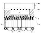
【0039】
次に、フリップチップ型半導体装置の半導体チップ2の裏面(図では上面)に、放熱性接着剤層41を介して、ヒートスプレッダ42を取り付け、図1に示す半導体装置32を得る。半導体チップ2で発生する熱は、放熱性接着剤層41を介して、ヒートスプレッダ42の広い表面から放熱される。
【0040】
ヒートスプレッダー42は、Cu、AL、W、Mo、Fe、Ni、Cr等の金属性材料を主成分として構成されているか、又は、アルミナ、ALN、SiC、ムライト等のセラミック材料から成る。放熱性接着剤41は、エポキシ系樹脂、シリコーン系樹脂、ポリイミド系樹脂、ポリオレフィン系樹脂、シアネートエステル系樹脂、フェノール系樹脂、ナフタレン系樹脂のいずれかの樹脂を主成分とし、Ag、Pd、Cu、AL、Au、Mo、W、ダイヤモンド、アルミナ、ALN、ムライト、BN、SiC等のセラミック材料から構成されている。
【0041】
一般的にフリップチップは、多ピン・高速系Logic系のデバイスに適用されることが多く、半導体チップ2の放熱の実行が重要である。本実施の形態では、ヒートスプレッダーを用いてその熱特性を向上させることが出来る。
【0042】
本実施の形態の半導体装置では、半導体チップとの熱膨張率の差が大きい有機系材料から成る多層配線基板を使用しないので、半導体チップと多層配線基板との間の応力による接続信頼性の低下は起こらない。従って、図5〜図16の一連の工程において、公知の多層配線基板のように、金属薄膜配線を10〜30μm程度に厚く形成して応力緩衝効果を持たせる必要はなく、その厚さは1μm程度で十分である。更に、半導体ウエハーのメタライズ製造方法とその製造装置を利用するので、フォトレジスト及び金属薄膜配線を1μm以下の薄い領域で加工処理することが容易になり、配線パターンの微細化を図ることが出来る。
【0043】
上述の製造工程、特に、多層配線層の形成工程において、高剛性の金属板16が、多層配線層の平面度を確保している。金属板16は剛性が高いので、全工程中で平面度が高く保持されており、金属板と多層配線層との間に線膨張差があっても、金属板に接合されてた多層配線層は内部応力の発生、及び膨張が抑えられ、そのソリが防止される。この結果、絶縁層及び配線部のパターニング時の不整合も生じず、歩留まりが良いという効果がある。
【0044】
この様に、金属層は、多層配線層の製造工程において効果を有するので、最終製品には存在しなくてもよい。金属板を除去した場合、多層配線層3の最下層が露出されるために、絶縁性樹脂薄膜18としては、有機系材料のようにそれ自身に外部応力からの柔軟性を有するものが好ましい。
【0045】
金属板16の除去は、本実施の形態の様に図16に示した工程の後で行わなければならないのではなく、多層配線層3に半導体チップ2を実装する工程の後に取り除いても良い。特に、半導体チップ2を実装する工程やヒートスプレッダー42を取り付ける工程等において、金属板16を残存させておけば、多層配線層3、半導体チップ2等に作用する機械的応力、熱的応力に起因する多層配線層の全体、その内部の各層、及びチップの歪みの発生を防ぐことが出来る。更に、多層配線層やチップの平面度を保持する必要がある工程では、取り除かずに、半田ボール13を接合する直前まで残存させておくことが好ましい。
【0046】
尚、本発明の半導体装置では、多層配線層は、金属板の片面のみに形成されており、非対称な構造となっているが、金属板は高剛性であるので、製造時、特に多層配線構造中の絶縁性樹脂薄膜層18製造時の応力による反りは生じない。また、金属板の両側に多層配線層を設けた場合に必要になるスルーホールの形成が不要であるので、スルーホール形成時に発生するゴミに起因する不良を防止することが出来、更に工程減によるコストの低減という効果も有する。
しかしながら、本実施の形態では、最終ユーザー側の回路基板への実装で用いる半田ボール13のスタンドオフ高さが低く、半導体装置と回路基板との間で生じる応力の緩衝を考慮していないので、両者間の接続信頼性には問題がある。この問題を解決するのが、以下に示す第2の実施の形態である。
【0047】
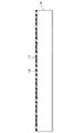
〔第2の実施の形態〕
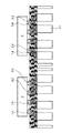
図21に、本発明によるフリップチップ型半導体装置の第2の実施の形態を示す。本実施の形態では、半導体チップ2が多層配線基板1に、フリップ実装されており、多層配線基板1は、第2基板層である多層配線層3と、第1基板層である緩衝層4とから構成されている。
【0048】
緩衝層4は、その一端が外部電極パッド部17に接続された複数金属層11から構成される。緩衝層4の周辺部、即ち複数金属層11の周囲部分には、閉じられた環状の支持枠25が設けられている。この支持枠は、製品のハンドリング時等に発生する機械的応力から多層配線構造部分(多層配線層)3を保護する効果を有する。
【0049】
複数金属層11の他端には、半田ボール13が接合されている。半田ボール13は、回路基板(図示せず)の電気的接合部に接合される。従って、緩衝層4が回路基板の電気的接合部に固着されることになる。
【0050】
この半導体装置では、半田ボール13が複数金属層11先端部に接合されており、外部端子としての半田ボール13を介して回路基板に実装される。この外部端子は、充分なスタンドオフ高さを有し、半導体装置とそれが実装される回路基板との間で生じる応力を主に複数金属層で緩衝する。従って、第1の実施の形態と比較して、回路基板と半導体装置との間の実装信頼性をより向上させることが出来る。
【0051】
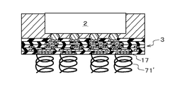
本実施の形態の半導体装置の製造方法は、第1の実施の形態の図4乃至図16に示す工程を行った後、図22(a)に示すように、多層配線層の下側に存在する金属板16を、フォトリソ技術が用いられるエッチング技術により選択的に除去する。その除去部分は、絶縁性樹脂薄膜層18に接する部分、即ち外部電極パッド部17に接しない部分である。このような選択的除去により、既述の複数金属層11を形成する。複数金属層11は、外部電極コラム部を形成している。
【0052】
この選択的除去は、図22(b)に示すように、金属版16の厚みの半分以上をレーザー加工、放電加工、あるいは部分切削加工等の手法により選択的にエッチング除去した後、レジストをマスクとして絶縁性樹脂薄膜層18表面が露出するまでエッチングして行うことが好ましい。特に、金属板16が500μm乃至3mm程度と大きな厚みを有する場合、1回のエッチング除去工程では外部電極コラムの直径寸法の制御が困難であり、更にエッチング時間が長くなるため、1回のエッチング除去工程中にレジストパターン部分が落下し、選択的除去が出来ないといった問題がある。本実施の形態に示すように、金属板16厚みの半分以上を選択的に除去した後、レジストをマスクとして再度エッチングを行い外部電極コラム部を形成することにより、500μm乃至3mm程度と厚みの大きい金属板16を確実に選択エッチングして、充分な高さを有する外部電極コラム部を形成することが出来る。この結果、後の工程で形成する半田ボール13のスタンドオフ高さを大きくし、回路基板に対する実装信頼性向上を図ることが出来る。
【0053】
次に、外部電極コラム部11の端部表面、及びパッド電極部23表面に、半田との密着性を向上させるために、それぞれNi/Au等のメッキ処理を施す。次に、図23に示すように、多層配線基板の集合体に対して単位多層配線基板毎に電気試験を行い、電気的に良品と判定された多層配線基板のみに、図23に示すように半導体チップ2に設けられたバンプ電極14を介して半導体チップ2を実装する。
【0054】
次に、図24に示す樹脂封止を行い、図25に示すように、外部電極コラム部11の端部表面に、外部端子として半田ボール13を接合する。この際、外部電極コラム部11にFluxを選択的に塗布後、搭載した半田ボール13に対しIRリフロー工程による加熱処理を施すことが好ましい。従って、本実施の形態では、金属板16として、剛性が高く、半田との濡れ性の良好な材料を用いることが好ましい。上記条件を満たし、半田ボール13と外部電極パッド部17とを電気的に接続できる材料であれば、金属に限られない。
【0055】
次に、図26に示すように半導体装置の個片処理を行い、複数のフリップチップ型半導体装置を作製する。次に、第1の実施の形態に示した方法により半導体チップの裏面にヒートスプレッダを取り付け、図21に示した半導体装置を得る。
【0056】
本実施の形態では、半田ボール13が外部電極コラム11の上に形成されており、スタンドオフ高さが大きい。従って、半導体装置とそれが実装される最終ユーザーの回路基板との間の熱膨張率の差に起因する応力を、主に外部電極コラムのたわみにより緩和することが出来、両者間の接続信頼性が向上すると共に、多層配線層の歪み(反り)を抑制する効果もある。
【0057】
しかしながら、この応力は外部電極パッド部17と外部電極コラム部11との接続部分に集中する傾向があるので、当該部分において外部電極コラムの接続不良が生じ易いという問題がある。この問題を解決するのが、以下に示す第3の実施の形態である。
【0058】
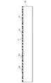
〔第3の実施の形態〕
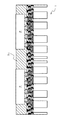
図27に、本発明によるフリップチップ型半導体装置の第3の実施の形態を示す。本実施の形態が第2の実施の形態と異なる点は、第1基板層である緩衝層4が、複数金属層11と複数応力吸収層12とから構成されている点である。
図27に示すように、緩衝層4を構成する複数金属層11と複数応力吸収層12は、多層配線層3と緩衝層4との対向方向に直交する方向に交互に配置されている。複数応力吸収層12は、シリコーン系樹脂により形成され、歪み力、応力を吸収する物理的性質を有する多層構造を有する。
【0059】
複数応力吸収層12としては、その他に、エポキシ系樹脂、ポリイミド系樹脂、ポリオレフィン系樹脂、シアネートエステル系樹脂、フェノール系樹脂、ナフタレン系樹脂等の有機絶縁材料のいずれかの樹脂を主成分として構成する。
【0060】
図28は、図27に示す半導体装置を半田ボール13側の底面から見た平面図である。複数応力吸収層12は、縦横に帯状に延び格子状に単一化された一体物(単体)であり、複数金属層11は、格子点に島状に配置されている。両者の体積比率、配列構造の変更は、半導体チップ、多層配線層3、及び緩衝層4が接合される回路基板から成る製品全体の仕様に対応する。緩衝層4の周辺部、即ち複数金属層11の周囲部分は閉じられた環状の支持枠25が設けられている。この支持枠は、後工程のハンドリング時等に発生する機械的応力から多層配線構造部分3を保護する効果を有する。但し、緩衝層4の緩衝性を高めるためには、支持枠は削除する方が好ましい。
【0061】
この緩衝層4は、多層配線層3よりも高い剛性を有している。それに加え、この部分にかかる応力の緩衝性も有する。
【0062】
本実施の形態の半導体装置の製造方法は、第2の実施の形態の図22に示す工程を行った後、図29に示すように、複数金属層11間及び複数金属層11と支持枠25との間の空間領域26(図22(a)参照)に絶縁性応力緩衝樹脂12を埋め込み、既述の複数応力吸収層12を形成する。この絶縁性応力緩衝樹脂12は、スピンコーティング法又はトランスファー封止技術等により形成され、多層配線層3及び外部電極コラム部11を機械的及び化学的応力から保護する効果を有する。
【0063】
続いて、外部電極コラム部11の端部表面が絶縁性応力緩衝樹脂12により覆われている場合には、CMP(Chemical Mechanical Polishing)技術、プラズマ表面技術で外部電極コラム部11の端部表面を覆う絶縁性応力緩衝樹脂12を除去する。
【0064】
次に、外部電極コラム部11の端部表面、及びパッド電極部23表面にそれぞれNi/Au等のメッキ処理を施す。その後、第2の実施の形態の図23乃至図26と同様にして、半導体チップの実装、樹脂封止、半田ボールの接合及び個片処理を行い、図27に示す半導体装置を得る。
【0065】
本実施の形態の半導体装置では、第2の実施の形態と同様に、半田ボール13が絶縁性応力緩衝樹脂12に囲まれた外部電極コラム11の上に形成されており、スタンドオフ高さが大きい。従って、半導体装置とそれが実装される最終ユーザーの回路基板との間の熱膨張率の差に起因する応力を、外部電極コラムのたわみにより緩和することが出来、両者間の接続信頼性が向上する。
【0066】
更に、この応力を、緩衝層4の絶縁性応力緩衝樹脂12で吸収するので、外部電極コラムの外部電極パッドに対する接続信頼性を低下させることがない。更に、緩衝層の応力吸収効果により、半導体装置と回路基板との間の接続信頼性を高めることが出来る。
【0067】
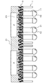
〔第4の実施の形態〕
図30に、本発明によるフリップチップ型半導体装置の第4の実施の形態を示す。本実施の形態が、第3の実施の形態と異なる点は、フリップチップ型半導体装置32の半導体チップ2の裏面(図では上面)に、放熱性接着剤層41を介して、ヒートスプレッダ42が設けられている点である。半導体チップで発生する熱は、放熱性接着剤層41を介してヒートスプレッダ42の広い表面から放熱される。ヒートスプレッダ42と放熱性接着剤41の構成は、第1の実施の形態と同様である。
【0068】
本実施の形態の半導体装置では、第3の実施の形態と比較して放熱性を向上させることが出来る。
【0069】
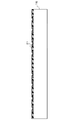
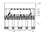
〔第5の実施の形態〕
図31は、本発明によるフリップチップ型半導体装置の第5の実施の形態を示す。本実施の形態が第3の実施の形態と異なる点は、半導体チップ2と多層配線層3との間に、絶縁性樹脂31を設けずに、アンダーフィル樹脂層43を設けている点である。この形成の後に、スティフナー44を介在させてヒートスプレッダ42を多層配線層3に取り付ける。
【0070】
アンダーフィル樹脂としては、エポキシ系樹脂、シリコーン系樹脂、ポリイミド系樹脂、ポリオレフィン系樹脂、シアネートエステル系樹脂、フェノール系樹脂、ナフタレン系樹脂のいずれかの樹脂を主成分として構成されている。
本実施の形態では、既述の第1乃至第3の実施の形態で使用されているインジェクション方式又はトランスファー封止方式による絶縁性樹脂31を使用せず、従来のフリップチップ型半導体装置の製造技術の主流であるアンダーフィル樹脂43を用いるので、特別な製造装置を用いる必要がないという利点がある。
【0071】
本実施の形態において、アンダーフィル樹脂43は多層配線層3上の一部を覆うだけであるが、スティフナー44を取り付けることで多層配線層3である多層配線基板の平面度を確保している。スティフナー44は、金属又はセラミック材料から形成されており、接着剤45を用いて多層配線層3に取り付ける。その後、半導体チップ2の裏面に放熱性接着剤41を介して放熱用のヒートスプレッダー42を取り付ける。
【0072】
〔第6の実施の形態〕
第1の実施の形態の半導体装置では、外部電極パッド部17に対する半田ボール13の接着性が不足であるという問題がある。これを解決するのが、以下に示す第6の実施の形態である。
【0073】
図32は、本発明の半導体装置の第6の実施の形態であり、図33及び図34にその製造方法を示す。本実施の形態の製造方法では、第1の実施の形態の図4乃至図20に示す工程を行った後、図33に示すように、多層配線層3に対向させてサポート板51を設ける。サポート板51には、半田ボールの配置パターンと同じ配置パターンで半田ボール挿入孔52が形成されており、半田ボール挿入孔52の直径は、半田ボール13の直径より大きい。サポート板51には、更に、樹脂注入口53が開けられている。サポート板51の材質としては、絶縁性材料であるか導電性材料であるかは問わない。
【0074】
続いて、図34に示すように、樹脂注入口53から樹脂を注入する。この樹脂は、絶縁性樹脂薄膜層18の表面、半田ボール13の側面、及びサポート板51の内周面とで形成される空間を埋めて注入層54を形成する。このような樹脂注入により、外部電極パッド部17と半田ボール13との接合を強化する。次に、ダイシングプレートを用いて、フリップチップ型多層配線半導体装置の個片処理を行い、図32に示すフリップチップ型多層配線半導体装置を得る。
【0075】
サポート板51は、樹脂注入時に注入された樹脂の表面高さを規定する効果がある。この結果、回路基板への接続面となる半田ボール13の頂部表面を確実に樹脂から露出させることが出来る。
【0076】
図35は、図32中の円内部Aを拡大してその詳細を示している。円内部Aは、外部電極コラム11の端部表面に接合された半田ボール13の周辺領域である。半田ボール13の球面と、半田ボール挿入孔52の内周面と、絶縁性樹脂薄膜層18表面とで形成される空間領域が注入層54により埋め尽くされ、半田ボール13と外部電極パッド部17とが強固に接合されている。
【0077】
本実施の形態の半導体装置では、樹脂補強効果により、半導体装置1の回路基板への実装時、その部分の応力変形を防止し、最終的な組付であるPKG形態の基板実装信頼性を向上させることが出来る。
【0078】
〔第7の実施の形態〕
図36は、本発明の半導体装置の第7の実施の形態である。本実施の形態が、第3の実施の形態と異なる点は、サポート板51及び注入層54が設けられている点である。応力吸収層12の表面、半田ボール13の側面、及びサポート板51の内周面で形成される空間に樹脂が注入され注入層54を形成し、半田ボール13と外部電極コラム11との接合を補強している。この結果、第6の実施の形態と同様に、半導体装置1の回路基板への実装時の応力変形を防止し、実装信頼性を向上させることができる。
【0079】
本実施の形態の製造方法は、第3の実施の形態の図29に示す工程及び図23乃至図26と同様の工程を行った後、図37に示すように、多層配線基板1にサポート板51を挿入する。次に、図38に示すように、サポート板の樹脂注入口53から樹脂を注入し、絶縁性応力緩衝樹脂12の表面、半田ボール13の側面、及びサポート板51の内周面で形成される空間を埋めて注入層54を形成する。
【0080】
これにより、外部電極コラム部11と半田ボール13との接合を補強出来、半導体装置の回路基板への実装時、その部分の応力変形を防止し、実装信頼性を向上出来る。
【0081】
〔第8の実施の形態〕
図39は、本発明の半導体装置の第8の実施の形態を示す。本実施の形態が図30に示す第4の実施の形態と異なる点は、サポート板51及び注入層54が追加されている点であり、第4の実施の形態と比較して、図35に示す樹脂補強効果が追補されている。
【0082】
〔第9の実施の形態〕
図40は、本発明の半導体装置の第9の実施の形態を示す。本実施の形態が図31に示す第5の実施の形態と異なる点は、サポート板51及び注入層54が追加されている点であり、第5の実施の形態と比較して、図35に示す樹脂補強効果が追補されている。
【0083】
〔第10の実施の形態〕
図41は、本発明の半導体装置の第10の実施の形態を示す。本実施の形態の半導体装置の製造方法は、第1の実施の形態の図4乃至図16に示す工程を行った後、図17に示すように、金属板16をエッチング技術により完全に削除する。金属板16の平面度維持の役目は、多層配線構造を形成した後には不要であるため、完全に除去しても問題ない。エッチング速度を大きくするため、そのエッチング特性を考慮し、薬液使用によるウエットエッチング法を用いる。
【0084】
次に、図18及び図19に示す工程を行い、その後、図42に示すように、多層配線構造3の最下層に形成されている金属配線層22(又は17)に、導電性接着剤61を用いて導電性コラム電極11’を接合する。導電性接着剤61の材料としては、金属配線層22と導電性コラム電極11’の両方の金属に対して濡れ性がよい材料が好ましい。
【0085】
次に、図43に示すように、応力吸収層12’を形成する。応力吸収層12’は、複数導電性コラム電極11’の間を埋め、且つ多層配線構造3の最下層の表面を被覆しており、導電性コラム電極11’と多層配線構造3とを機械的応力と化学的応力から保護する。
【0086】
次に、導電性コラム電極11’の端部表面の樹脂除去処理及びメッキ処理を行った後、図25に対応する方法で図44に示すように、導電性コラム電極11’の端部表面に半田ボール13を接合する。
【0087】
更に、導電性コラム電極11’に対する半田ボール13の接着強度が不足している場合には、図37に対応する方法で図45に示すように、サポート板51を取り付ける。更に、図38に対応する方法で図46に示すように樹脂注入を行い、導電性コラム電極11’と半田ボールとの接合を樹脂補強し、図41に示す半導体装置を得る。
【0088】
本実施の形態は、第3の実施の形態等では必要であった外部電極コラム部11を形成するための金属板16の選択的なエッチングの工程が無い。従って、エッチングの金属板面内でのばらつきを考慮する必要が無いという特徴がある。つまり、金属板16を完全に除去した後、多層配線層3の外部電極パッド部17に予め形成した導電性コラム電極11’を接合させることが出来る。
【0089】
〔第11の実施の形態〕
図47は、本発明の半導体装置の第11の実施の形態を示す。本実施の形態では、第10の実施の形態の図42に示す工程を行い導電性コラム電極11’を形成した後、多層配線層に対向させてサポート板51’を設ける。その後、絶縁性樹脂薄膜層18の表面、導電性コラム電極11’の側壁、半田ボール13の側面、及びサポート板51’の内周面で形成される空間に樹脂注入を行い注入層54を形成する。
【0090】
本実施の形態では、第10の実施の形態と比較して、応力吸収層12’を形成する工程、及び応力吸収層12’形成後、導電性コラム電極11’の半田ボール接合面の樹脂除去工程が省略されており、プロセスを短縮し、コストを削減する効果がある。更に、第10の実施の形態と比較して、厚みの大きいサポート板を用いるので、注入される樹脂量が多くサポート板にかかる圧力が大きいにも関わらず、この圧力に抗してサポート板表面を平坦に保ち、注入された樹脂の表面高さを規定することが出来る。この結果、回路基板への接続面となる半田ボール13の頂部表面を確実に樹脂から露出させることが出来る。
【0091】
〔第12の実施の形態〕
図48は、本発明の半導体装置の第12の実施の形態を示している。本実施の形態では、ピン形状の外部電極71が外部電極パッド部17に直接に接合されている。ピン形状の外部電極71は、主に金属合金で形成され、それ自体が剛性を有している。また、その一端で回路基板に接合する側が、その他端で外部電極パッド部に接合する側よりも細い形状をしているので、フレキシブルである。従って、最終ユーザーが回路基板へ実装した後、外部応力に対して緩衝性を有し、接続信頼性が高い。更に、ピン先端部が細い形状であるので、微細なパターンを有する回路基板への実装が可能になるという特徴がある。
【0092】
〔第13の実施の形態〕
図49は、本発明の半導体装置の第13の実施の形態を示す。本実施の形態では、スプリング状の外部電極71’が外部電極パッド部17に直接に接合されている。外部電極71’の側面部分を絶縁体で被覆しても良い。外部電極71’は、螺旋状の弾性体であり、それ自体に剛性はないが、その柔構造によって緩衝性に優れている。従って、最終ユーザーが回路基板へ実装した後も、外部応力に対して優れた緩衝性を有する。
【0093】
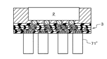
第12、13の実施の形態は、外部電極コラム部11を形成するための金属板16の選択的なエッチングを行う必要が無いので、エッチングの金属板面内でのばらつくを考慮する必要が無いという特徴がある。つまり、金属板16を完全に除去した後、多層配線構造3の外部電極パッド部17に予め形成した外部電極71、71’を接合させることができる。
【0094】
〔第14の実施の形態〕
図50は、本発明の半導体装置の第14の実施の形態を示す。本実施の形態では、柱状の外部電極71”が導電性接着剤により、外部電極パッド部17に直接に接合されている。外部電極71”は、それ自体に緩衝性はないが、剛性を有しているので、半導体装置全体の剛性を強化し、ハンドリング時や回路基板への実装時においても多層配線構造部分の平坦性を確保する。また、フレキシビリティーには乏しいが、スタンドオフ高さが大きいので、回路基板への実装信頼性は高い。
【0095】
〔第15の実施の形態〕
図51は、第2の実施の形態の変形例であり、図22に示す工程において、金属板16のエッチング条件を適当に設定することにより、金属層11A又は格子体11Aが、逆エンタシス形状を有し、中細りの鼓状に形成されている。逆エンタシス形状は、高さ方向長さは一定であるが横方向の太さが変化しており、横方向に受ける応力をより有効に吸収することができる。
【0096】
多層配線構造の形成時の剛性、外部電極が接合された後にも継続される剛性、外部電極が接合された後の剛性と緩衝性、外部電極自体が持つ剛性、外部電極部分自体が持つ柔軟性、外部電極自体が持つ剛性と柔軟性は、それぞれに、製品の利用状態に応じて適正に評価され実施されることになる。多層配線構造の形成時の剛性は、あらゆる場合に共通する優れた工程上の物性である。
【0097】
本発明の半導体装置は、実施の形態を通じて明らかにされたように、半導体チップとの熱膨張係数の差の大きなガラスエポキシ基板を介さずに半導体チップを回路基板に実装できるので、半導体チップとガラスエポキシ基板間の応力緩衝を目的として配線パターンの膜厚を大きくする必要は無く、配線基板において微細な配線パターン形成が可能になる。この結果、多層配線基板単体の外形寸法を縮小することが出来、装置の微細化が可能になる。更に、一枚の大パネルから製造できる多層配線基板の枚数を増加させることが出来、コストの削減が可能になる。
【0098】
更に、本発明の半導体装置の多層配線構造は、半導体ウエハレベルの加工処理により形成できるので、従来の多層配線基板と比較して大幅に工程を削減することが出来、配線パターンの微細化を容易に行うことが出来る。
【0099】
本発明の半導体装置が有する柱状の導電体は、半導体装置とそれが実装される回路基板との間の応力を緩和する効果を有し、両者間の接続の信頼性を向上させることが出来る。
【0100】
本発明の半導体装置の製造方法では、金属板上に多層配線層を形成するので、製造中の熱処理等で配線層中に応力が発生しても、配線層は剛性の高い金属板に固着されているので反りが抑制され、微細なパターンを確実に形成できる。
【0101】
【発明の効果】
本発明による配線基板、配線基板を有する半導体装置、及び、その製造方法、実装方法は、信頼性が高い多層化配線基板を有する半導体装置を提供することができ、信頼性が高い実装を可能にする。
【図面の簡単な説明】
【図1】図1は、本発明による半導体装置の実施の形態を示す断面図である。
【図2】図2は、図1の底面図である。
【図3】図3は、多層配線層の一部を示す断面図である。
【図4】図4は、本発明による半導体装置の製造方法の実施の形態を示す断面図である。
【図5】図5は、図4の次のステップを示す断面図である。
【図6】図6は、図5の次のステップを示す断面図である。
【図7】図7は、図6の次のステップを示す断面図である。
【図8】図8は、図7の次のステップを示す断面図である。
【図9】図9は、図8の次のステップを示す断面図である。
【図10】図10は、図9の次のステップを示す断面図である。
【図11】図11は、図10の次のステップを示す断面図である。
【図12】図12は、図11の次のステップを示す断面図である。
【図13】図13は、図12の次のステップを示す断面図である。
【図14】図14は、図13の次のステップを示す断面図である。
【図15】図15は、図14の次のステップを示す断面図である。
【図16】図16は、図15の次のステップを示す断面図である。
【図17】図17は、図16の次のステップを示す断面図である。
【図18】図18は、図17の次のステップを示す断面図である。
【図19】図19は、図18の次のステップを示す断面図である。
【図20】図20は、最終品を示す断面図である。
【図21】図21は、本発明による半導体装置の実施の他の形態を示す断面図である。
【図22】図22(a),(b)は、製造の各ステップを示す断面図である。
【図23】図23は、次のステップを示す断面図である。
【図24】図24は、更に次のステップを示す断面図である。
【図25】図25は、更に次のステップを示す断面図である。
【図26】図26は、更に次のステップを示す断面図である。
【図27】図27は、本発明による半導体装置の実施の更に他の形態を示す断面図である。
【図28】図28は、図27の底面図である。
【図29】図29は、製造のステップを示す断面図である。
【図30】図30は、本発明による半導体装置の実施の更に他の形態を示す断面図である。
【図31】図31は、本発明による半導体装置の実施の更に他の形態を示す断面図である。
【図32】図32は、本発明による半導体装置の実施の更に他の形態を示す断面図である。
【図33】図33は、製造のステップを示す断面図である。
【図34】図34は、次のステップを示す断面図である。
【図35】図35は、図32の一部を示す断面図である。
【図36】図36は、本発明による半導体装置の実施の更に他の形態を示す断面図である。
【図37】図37は、製造のステップを示す断面図である。
【図38】図38は、次のステップを示す断面図である。
【図39】図39は、本発明による半導体装置の実施の更に他の形態を示す断面図である。
【図40】図40は、本発明による半導体装置の実施の更に他の形態を示す断面図である。
【図41】図41は、本発明による半導体装置の製造方法の実施の更に他の形態を示す断面図である。
【図42】図42は、本発明による半導体装置の実施の更に他の形態を示す断面図である。
【図43】図43は、製造のステップを示す断面図である。
【図44】図44は、次のステップを示す断面図である。
【図45】図45は、更に次のステップを示す断面図である。
【図46】図46は、更に次のステップを示す断面図である。
【図47】図47は、本発明による半導体装置の実施の更に他の形態を示す断面図である。
【図48】図48は、本発明による半導体装置の実施の更に他の形態を示す断面図である。
【図49】図49は、本発明による半導体装置の実施の更に他の形態を示す断面図である。
【図50】図50は、本発明による半導体装置の実施の更に他の形態を示す断面図である。
【図51】図51は、本発明による半導体装置の実施の更に他の形態を示す断面図である。
【図52】図52は、公知のフリップチップ型半導体装置を示す正面図である。
【図53】図53は、公知のフリップチップ型半導体装置の実装を示す正面図である。
【図54】図54は、公知のフリップチップ型半導体装置の製造方法を示す断面図である。
【図55】図55は、図54の次のステップを示す断面図である。
【図56】図56は、図55の次のステップを示す断面図である。
【図57】図57は、図56の次のステップを示す断面図である。
【図58】図58、図57の次のステップを示す断面図である。
【図59】図59は、図58の次のステップを示す断面図である。
【符号の説明】
2…半導体装置(半導体チップ)
3…配線層、多層配線層(第2基板層)
4…緩衝層(第1基板層)
5−2…第1絶縁層
11,11’…複数金属層(導電体)
12,12’…複数応力吸収層
13…半田ボール
14…バンプ電極(外部電極端子)
16…金属板
17外部電極パッド
19…第1の開口
23…パッド電極
24,9−2…第2絶縁層
41…熱伝達性接着剤
42…放熱体
44…スティフナー
51…支持体
71,71’…導電性支柱[0001]
BACKGROUND OF THE INVENTION
The present invention relates to a wiring board, a semiconductor device having the wiring board, a method for manufacturing the wiring board, and a method for mounting the semiconductor device on the wiring board, and in particular, a flip chip type semiconductor chip is mounted on the multilayered wiring board. The present invention relates to a wiring board, a semiconductor device having the wiring board, a manufacturing method thereof, and a mounting method.
[0002]
[Prior art]
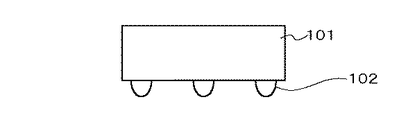
In recent years, the importance of flip chip type semiconductor devices has increased as a semiconductor device capable of high-density mounting. FIG. 52 shows a conventional flip chip type semiconductor device. The flip chip type semiconductor chip 101 is provided with an external terminal (not shown) formed in a predetermined area array arrangement on the peripheral portion or active region thereof, and provided on the external terminal, solder, Au, Sn-Ag system And
[0003]
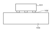
As shown in FIG. 53, the flip-chip type semiconductor chip 101 is mounted on a
[0004]
Such a mounting method has a problem that the temperature cycle characteristic is particularly inferior in the mounting reliability due to the difference in the linear expansion coefficient between the multilayer wiring board and the flip chip type semiconductor chip 101. In order to solve this problem, the following measures have been taken conventionally.
[0005]
First, the first method is a method using a ceramic material such as AlN, mlide, or glassercer that has a small difference in coefficient of linear expansion from silicon of a semiconductor chip as a multilayer wiring board. Although this method is effective from the viewpoint of improving mounting reliability, it uses an expensive ceramic material as the material of the multilayer wiring board, so the scope of application is limited to a high-end supercomputer or a specific use of a large computer. Is done.
[0006]
As a second method, there is a method using a multilayer wiring board made of an organic material which has a larger linear expansion coefficient than silicon of a semiconductor chip but is relatively inexpensive. In this method, an underfill resin is provided between the semiconductor chip and the multilayer wiring board. As a result, the shear stress acting on the bump portion connecting the semiconductor chip and the multilayer wiring board can be dispersed in the underfill resin covering the bump, thereby improving the mounting reliability.
[0007]
As the multilayer wiring board using the organic material used in the second method, a multilayer wiring board usually called a build-up board is used because of the minimum pitch of the bump arrangement pattern and the number of pins. A method for manufacturing this build-up substrate is shown in FIGS.
[0008]
First, as shown in FIG. 54, a
[0009]
Next, as shown in FIG. 55, an
Next, as shown in FIG. 56, a metal
[0010]
[Problems to be solved by the invention]
The multilayer wiring board used in the second method is formed of a glass epoxy base material that is relatively inexpensive and excellent in processability for forming a through hole. The glass epoxy base material has a difference in thermal expansion coefficient from that of a semiconductor chip. Therefore, stress is generated between the two, and the reliability of connection is lowered. Therefore, for the purpose of relaxing this stress, the wiring pattern formed on the glass epoxy base material has a film thickness of about 10 to 30 μm. Accordingly, the photoresist or dry film used as a mask at the time of wiring patterning needs to have a thickness of about 20 to 40 μm. As a result, the pattern pitch and the wiring pattern pitch in the exposure / development process are at least about 30 μm, and there is a problem that it is not possible to increase the density of the multilayer wiring board and reduce the size of the board.
[0011]
Thus, since the conventional multilayer wiring board uses a glass epoxy base material, the outer dimensions of the multilayer wiring board cannot be reduced with the necessary rewiring function. Therefore, although the base material itself is inexpensive, the number of multilayer wiring boards that can be manufactured from one large panel is small, and it is difficult to reduce the cost of the multilayer wiring board. Further, in the glass epoxy base material, warping due to stress at the time of forming the
[0012]
An object of the present invention is to solve these problems by forming a multilayer wiring layer on a metal plate and to provide a highly reliable multilayer wiring board.
[0013]
[Means for Solving the Problems]
The method for manufacturing a semiconductor device of the present invention includes a step of selectively forming an external electrode pad on a metal plate, and a step of forming a first insulating layer having a first opening at a position corresponding to the external electrode pad. And electrically connecting to the external electrode pad through the first opening.FirstForming a wiring layer; andFirstForming a second insulating layer having a second opening at a position corresponding to the wiring layer; and through the second opening,FirstElectrically connected to the wiring layerForming a second wiring layerProcess,Selectively removing the portion of the metal plate in contact with the first insulating layer by etching to form a columnar conductor having one end in contact with the external electrode pad and electrically connected to the external electrode pad; A step of mounting a semiconductor chip connected to two wiring layers via an external electrode, a step of forming an insulating resin layer between the columnar conductors, a circuit board and the other end of the columnar conductors Forming an external terminal for electrically connecting the external electrode terminal of the semiconductor chip; A support plate having an opening at a position corresponding to the external terminal is provided on the insulating resin layer and bonded to a space surrounded by the surface of the insulating resin layer, the side surface of the external terminal, and the inner peripheral surface of the support plate. Inject resinAnd a process.The method for manufacturing a semiconductor device of the present invention includes a step of forming an external electrode pad directly on a metal plate, and a step of forming a first insulating layer having a first opening at a position corresponding to the external electrode pad. Forming a first wiring layer electrically connected to the external electrode pad through the first opening; and a second insulating layer having a second opening at a position corresponding to the first wiring layer Forming a second wiring layer electrically connected to the first wiring layer through the second opening, and etching the metal plate so that at least the external electrode pad is exposed. After the step of removing, the step of etching away the metal plate, a step of connecting one end of a columnar conductor to the external electrode pad using a conductive adhesive, and an external electrode terminal on the second wiring layer Semiconductor chip connected via Electrically connecting a circuit board and an external electrode terminal of the semiconductor chip to the other end of the columnar conductor, and a step of forming an insulating resin layer between the columnar conductors. A support plate having an opening at a position corresponding to the external terminal is provided on the insulating resin layer, and the surface of the insulating resin layer, the side surface of the external terminal, and the inside of the support plate And a step of injecting an adhesive resin into a space surrounded by the peripheral surface.The method for manufacturing a semiconductor device of the present invention includes a step of forming a multilayer wiring layer on a metal plate, and the wiring layer has high rigidity even if stress is generated in the wiring layer due to heat treatment during manufacturing. Since it is fixed to the metal plate, warping is suppressed, and a fine pattern can be reliably formed.
[0014]
In this way, since the semiconductor chip can be mounted on the circuit board without using a glass epoxy substrate having a large difference in thermal expansion coefficient from the semiconductor chip, the wiring pattern film is used for buffering the stress between the semiconductor chip and the glass epoxy board. There is no need to increase the thickness.
[0015]
The semiconductor device of the present invention is provided with an external electrode pad and the external electrode pad.,In the corresponding position of the external electrode padIt is formedFirst openingAnd a lower surface that is substantially flat with the surface of the external electrode padA first insulating layer having a first insulating layer, and the first insulating layer electrically connected to the external electrode pad through the first opening.FirstA wiring layer;FirstProvided on the wiring layerFirstA second insulating layer having a second opening at a corresponding position in the wiring layer; and the second opening through the second opening.FirstElectrically connected to the wiring layerA wiring substrate formed by a second wiring layer that is connected to and electrically connected to one end of the external electrode pad, and a columnar conductor provided independently for each external electrode pad; A semiconductor chip connected to the second wiring layer via an external electrode terminal; an external terminal for electrically connecting the circuit board and the external electrode terminal of the semiconductor chip to the other end of the columnar conductor; A plurality of the columnar conductors, the plurality of conductors being insulated from each other via an insulating resin, and configured by the plurality of columnar conductors and the insulating resin. The board layer has higher rigidity than the wiring board.It is characterized by that.
The semiconductor device of the present invention is substantially provided with an external electrode pad, a first opening provided on an upper surface of the external electrode pad, and a surface of the external electrode pad formed at a corresponding position of the external electrode pad. A first insulating layer having a flat bottom surface, a first wiring layer electrically connected to the external electrode pad through the first opening and provided on the first insulating layer, and the first A second insulating layer provided on the wiring layer and having a second opening at a corresponding position of the first wiring layer; and a second wiring electrically connected to the first wiring layer through the second opening A wiring board formed by a layer and a columnar conductor that is electrically connected to the external electrode pad with a conductive adhesive at one end and provided independently for each external electrode pad; A semiconductor chip connected to the wiring layer via external electrode terminals; An external terminal for electrically connecting a circuit board and an external electrode terminal of the semiconductor chip to the other end of the columnar conductor, and a plurality of the columnar conductors, The conductors are insulated from each other via an insulating resin, and the substrate layer composed of the plurality of columnar conductors and the insulating resin has higher rigidity than the wiring board. .
The semiconductor device of the present invention is substantially provided with an external electrode pad, a first opening provided on an upper surface of the external electrode pad, and a surface of the external electrode pad formed at a corresponding position of the external electrode pad. A first insulating layer having a flat bottom surface, a first wiring layer electrically connected to the external electrode pad through the first opening and provided on the first insulating layer, and the first A second insulating layer provided on the wiring layer and having a second opening at a corresponding position of the first wiring layer; and a second wiring electrically connected to the first wiring layer through the second opening A wiring board formed by a layer, a columnar conductor that is electrically connected by joining one end to the external electrode pad, and provided independently for each external electrode pad; and the second wiring layer A semiconductor chip connected to the external electrode terminal via the external pillar, and the pillar An external terminal for electrically connecting a circuit board and an external electrode terminal of the semiconductor chip to the other end of the conductive body; and the columnar conductor in contact with the lower surface of the first insulating layer It has adhesive resin which covers a part of side wall of this, and a part of side wall of the said external terminal.
The semiconductor device of the present invention is substantially provided with an external electrode pad, a first opening provided on an upper surface of the external electrode pad, and a surface of the external electrode pad formed at a corresponding position of the external electrode pad. A first insulating layer having a flat bottom surface, a first wiring layer electrically connected to the external electrode pad through the first opening and provided on the first insulating layer, and the first A second insulating layer provided on the wiring layer and having a second opening at a corresponding position of the first wiring layer; and a second wiring electrically connected to the first wiring layer through the second opening A wiring board formed by a layer and a columnar conductor that is electrically connected to the external electrode pad with a conductive adhesive at one end and provided independently for each external electrode pad; A semiconductor chip connected to the wiring layer via external electrode terminals; The other end of the columnar conductor has an external terminal for electrically connecting the circuit board and the external electrode terminal of the semiconductor chip, and is in contact with the lower surface of the first insulating layer. It has adhesive resin that covers the side surface of the conductor and a part of the side wall of the external terminal. It is characterized by.
[0016]
The semiconductor device of the present invention includes a columnar conductor whose one end is connected to the external electrode pad, and the columnar conductor has an effect of relieving stress between the semiconductor device and the circuit board. The reliability of the connection between them can be improved.
[0017]
DETAILED DESCRIPTION OF THE INVENTION
[First Embodiment]
FIG. 1 shows a first embodiment of a flip-chip type semiconductor device according to the present invention. A
[0018]
As shown in FIG. 3, the
[0019]
The
[0020]
A flip chip
[0021]
4 to 20 show a method for manufacturing the semiconductor device of the present embodiment. As shown in FIG. 4, the
[0022]
Next, as shown in FIG. 5, after forming a thin film of Ti, Cr, Mo, W-based alloy to be an adhesive metal layer on the upper surface of the
[0023]
Next, as shown in FIG. 6, an insulating resin
[0024]
In addition to the polyimide resin, the insulating resin
[0025]
Next, as shown in FIG. 7, the insulating resin
[0026]
Next, as shown in FIG. 8, Ti, Cr, Mo, which are adhesive metal layers of the metal
[0027]
Next, using the photoresist as a mask, the metal
[0028]
Next, the photoresist is peeled off, and the metal thin film layer is etched using the wiring pattern as a mask to form the metal thin
[0029]
Next, as shown in FIG. 15, a
[0030]
Thereafter, in order to protect the
[0031]
As the solder resist film, an organic insulating material in which an inorganic filler such as a fine powder of silicon oxide is added to an epoxy resin is used. In addition, it is possible to select a material that is resistant to external mechanical stress, has high resistance to the flux cleaning solution and Au plating solution, and has excellent adhesion characteristics with a sealing material such as an underfill material.
If the insulating resin
[0032]
After these steps, as shown in FIG. 17, the
[0033]
Next, an electroless plating process such as Ni / Au or Zn / Ni / Au is performed on the
[0034]
Next, as shown in FIG. 18, the flip chip
[0035]
Next, as shown in FIG. 19, in order to protect the
[0036]
The insulating
[0037]
Next,
[0038]
Next, as shown in FIG. 20, using a dicing blade or the like, individual processing of the flip chip type semiconductor device is performed, and a plurality of flip chip type semiconductor devices are manufactured.
[0039]
Next, a
[0040]
The
[0041]
In general, the flip chip is often applied to a multi-pin high-speed logic device, and it is important to perform heat dissipation of the
[0042]
In the semiconductor device according to the present embodiment, a multilayer wiring board made of an organic material having a large difference in thermal expansion coefficient from the semiconductor chip is not used, so that connection reliability is reduced due to stress between the semiconductor chip and the multilayer wiring board. Does not happen. Accordingly, in the series of steps shown in FIGS. 5 to 16, it is not necessary to form a metal thin film wiring as thick as about 10 to 30 μm so as to have a stress buffering effect as in a known multilayer wiring board, and the thickness is 1 μm. The degree is sufficient. Furthermore, since the semiconductor wafer metallization manufacturing method and the manufacturing apparatus are used, it is easy to process the photoresist and the metal thin film wiring in a thin region of 1 μm or less, and the wiring pattern can be miniaturized.
[0043]
In the above-described manufacturing process, in particular, the multilayer wiring layer forming process, the high-
[0044]
As described above, the metal layer has an effect in the manufacturing process of the multilayer wiring layer, and therefore may not be present in the final product. When the metal plate is removed, the lowermost layer of the
[0045]
The removal of the
[0046]
In the semiconductor device of the present invention, the multilayer wiring layer is formed on only one side of the metal plate and has an asymmetric structure. However, since the metal plate is highly rigid, the multilayer wiring structure is particularly produced during manufacture. There is no warping due to stress during the production of the insulating resin
However, in the present embodiment, the standoff height of the
[0047]
[Second Embodiment]
FIG. 21 shows a second embodiment of a flip-chip type semiconductor device according to the present invention. In the present embodiment, the
[0048]
The
[0049]
A
[0050]
In this semiconductor device, a
[0051]
The semiconductor device manufacturing method of the present embodiment exists under the multilayer wiring layer as shown in FIG. 22A after performing the steps shown in FIGS. 4 to 16 of the first embodiment. The
[0052]
In this selective removal, as shown in FIG. 22B, more than half of the thickness of the
[0053]
Next, the end surface of the external
[0054]
Next, resin sealing shown in FIG. 24 is performed, and as shown in FIG. 25,
[0055]
Next, as shown in FIG. 26, individual processing of the semiconductor device is performed to manufacture a plurality of flip chip type semiconductor devices. Next, a heat spreader is attached to the back surface of the semiconductor chip by the method shown in the first embodiment, and the semiconductor device shown in FIG. 21 is obtained.
[0056]
In the present embodiment, the
[0057]
However, since this stress tends to concentrate on the connection portion between the external
[0058]
[Third Embodiment]
FIG. 27 shows a third embodiment of a flip-chip type semiconductor device according to the present invention. The present embodiment is different from the second embodiment in that the
As shown in FIG. 27, the plurality of
[0059]
In addition, the multiple
[0060]
FIG. 28 is a plan view of the semiconductor device shown in FIG. 27 as viewed from the bottom surface on the
[0061]
The
[0062]
In the method of manufacturing the semiconductor device of the present embodiment, after performing the step shown in FIG. 22 of the second embodiment, as shown in FIG. 29, between the
[0063]
Subsequently, when the end surface of the external
[0064]
Next, the end surface of the external
[0065]
In the semiconductor device of the present embodiment, the
[0066]
Furthermore, since this stress is absorbed by the insulating
[0067]
[Fourth Embodiment]
FIG. 30 shows a fourth embodiment of a flip-chip type semiconductor device according to the present invention. This embodiment is different from the third embodiment in that a
[0068]
In the semiconductor device of the present embodiment, the heat dissipation can be improved as compared with the third embodiment.
[0069]
[Fifth Embodiment]
FIG. 31 shows a fifth embodiment of a flip-chip type semiconductor device according to the present invention. This embodiment is different from the third embodiment in that an underfill resin layer 43 is provided between the
[0070]
The underfill resin is composed mainly of any one of an epoxy resin, a silicone resin, a polyimide resin, a polyolefin resin, a cyanate ester resin, a phenol resin, and a naphthalene resin.
In this embodiment, the conventional flip-chip type semiconductor device manufacturing technique is used without using the insulating
[0071]
In the present embodiment, the underfill resin 43 only covers a part on the
[0072]
[Sixth Embodiment]
The semiconductor device according to the first embodiment has a problem that the adhesion of the
[0073]
FIG. 32 shows a sixth embodiment of the semiconductor device of the present invention, and FIGS. 33 and 34 show the manufacturing method thereof. In the manufacturing method of the present embodiment, after the steps shown in FIGS. 4 to 20 of the first embodiment are performed, a
[0074]
Subsequently, as shown in FIG. 34, a resin is injected from the
[0075]
The
[0076]
FIG. 35 shows the details of an enlarged circle inside A in FIG. A circle inside A is a peripheral region of the
[0077]
In the semiconductor device of the present embodiment, due to the resin reinforcing effect, when the semiconductor device 1 is mounted on the circuit board, stress deformation of that portion is prevented, and the final mounting of the PKG-type board mounting reliability is improved. It can be made.
[0078]
[Seventh Embodiment]
FIG. 36 shows a seventh embodiment of the semiconductor device of the present invention. This embodiment is different from the third embodiment in that a
[0079]
In the manufacturing method of the present embodiment, the process shown in FIG. 29 of the third embodiment and the processes similar to FIGS. 23 to 26 are performed, and then, as shown in FIG. 51 is inserted. Next, as shown in FIG. 38, resin is injected from the
[0080]
As a result, the bonding between the external
[0081]
[Eighth Embodiment]
FIG. 39 shows an eighth embodiment of the semiconductor device of the present invention. This embodiment is different from the fourth embodiment shown in FIG. 30 in that a
[0082]
[Ninth Embodiment]
FIG. 40 shows a ninth embodiment of the semiconductor device of the present invention. This embodiment is different from the fifth embodiment shown in FIG. 31 in that a
[0083]
[Tenth embodiment]
FIG. 41 shows a semiconductor device according to a tenth embodiment of the present invention. In the method of manufacturing the semiconductor device of the present embodiment, after performing the steps shown in FIGS. 4 to 16 of the first embodiment, the
[0084]
Next, the steps shown in FIGS. 18 and 19 are performed, and then, as shown in FIG. 42, the
[0085]
Next, as shown in FIG. 43, a stress absorbing layer 12 'is formed. The
[0086]
Next, after performing resin removal treatment and plating treatment on the end surface of the
[0087]
Further, when the adhesion strength of the
[0088]
In the present embodiment, there is no selective etching step of the
[0089]
[Eleventh embodiment]
FIG. 47 shows an eleventh embodiment of semiconductor device according to the present invention. In the present embodiment, after performing the step shown in FIG. 42 of the tenth embodiment to form the
[0090]
In the present embodiment, as compared with the tenth embodiment, the step of forming the
[0091]
[Twelfth embodiment]
FIG. 48 shows a twelfth embodiment of the semiconductor device of the present invention. In the present embodiment, the pin-shaped
[0092]
[Thirteenth embodiment]
FIG. 49 shows a thirteenth embodiment of semiconductor device according to the present invention. In the present embodiment, a spring-like
[0093]
In the twelfth and thirteenth embodiments, there is no need to perform selective etching of the
[0094]
[Fourteenth embodiment]
FIG. 50 shows a fourteenth embodiment of semiconductor devices according to the present invention. In the present embodiment, the columnar
[0095]
[Fifteenth embodiment]
FIG. 51 is a modification of the second embodiment. In the step shown in FIG. 22, the
[0096]
Rigidity when forming a multilayer wiring structure, rigidity that continues even after the external electrode is joined, rigidity and buffering after the external electrode is joined, rigidity that the external electrode itself has, flexibility that the external electrode part itself has The rigidity and flexibility of the external electrode itself are appropriately evaluated and implemented according to the use state of the product. The rigidity at the time of forming the multilayer wiring structure is an excellent process property common to all cases.
[0097]
Since the semiconductor device of the present invention can be mounted on a circuit board without using a glass epoxy substrate having a large difference in thermal expansion coefficient from that of the semiconductor chip, as has been clarified through the embodiments, the semiconductor chip and the glass It is not necessary to increase the film thickness of the wiring pattern for the purpose of buffering stress between the epoxy substrates, and a fine wiring pattern can be formed on the wiring board. As a result, the outer dimensions of the multilayer wiring board alone can be reduced, and the apparatus can be miniaturized. Furthermore, the number of multilayer wiring boards that can be manufactured from a single large panel can be increased, and the cost can be reduced.
[0098]
Furthermore, since the multilayer wiring structure of the semiconductor device of the present invention can be formed by processing at the semiconductor wafer level, the number of processes can be greatly reduced compared to the conventional multilayer wiring board, and the miniaturization of the wiring pattern is easy. Can be done.
[0099]
The columnar conductor included in the semiconductor device of the present invention has an effect of relieving stress between the semiconductor device and a circuit board on which the semiconductor device is mounted, and can improve the reliability of connection between the two.
[0100]
In the method for manufacturing a semiconductor device according to the present invention, a multilayer wiring layer is formed on a metal plate. Therefore, even if stress is generated in the wiring layer due to heat treatment during manufacturing, the wiring layer is fixed to the metal plate having high rigidity. Therefore, warpage is suppressed and a fine pattern can be formed reliably.
[0101]
【The invention's effect】
The wiring board, the semiconductor device having the wiring board, the manufacturing method, and the mounting method according to the present invention can provide a semiconductor device having a highly reliable multilayer wiring board, and can be mounted with high reliability. To do.
[Brief description of the drawings]
FIG. 1 is a cross-sectional view showing an embodiment of a semiconductor device according to the present invention.
FIG. 2 is a bottom view of FIG. 1;
FIG. 3 is a cross-sectional view showing a part of a multilayer wiring layer.
FIG. 4 is a cross-sectional view showing an embodiment of a method of manufacturing a semiconductor device according to the present invention.
FIG. 5 is a cross-sectional view showing the next step of FIG. 4;
FIG. 6 is a cross-sectional view showing the next step of FIG. 5;
FIG. 7 is a cross-sectional view showing the next step of FIG. 6;
FIG. 8 is a cross-sectional view showing the next step of FIG. 7;
FIG. 9 is a cross-sectional view showing the next step of FIG. 8;
FIG. 10 is a cross-sectional view showing the next step of FIG. 9;
FIG. 11 is a cross-sectional view showing the next step of FIG. 10;
12 is a cross-sectional view showing the next step of FIG. 11. FIG.
FIG. 13 is a cross-sectional view showing the next step of FIG. 12;
FIG. 14 is a cross-sectional view showing the next step of FIG. 13;
FIG. 15 is a cross-sectional view showing the next step of FIG. 14;
FIG. 16 is a cross-sectional view showing the next step of FIG. 15;
FIG. 17 is a cross-sectional view showing the next step of FIG. 16;
FIG. 18 is a cross-sectional view showing the next step of FIG. 17;
FIG. 19 is a cross-sectional view showing the next step of FIG. 18;
FIG. 20 is a cross-sectional view showing a final product.
FIG. 21 is a cross-sectional view showing another embodiment of a semiconductor device according to the present invention.
22 (a) and 22 (b) are cross-sectional views showing the respective steps of manufacture.
FIG. 23 is a cross-sectional view showing the next step.
FIG. 24 is a cross-sectional view showing a further next step.
FIG. 25 is a cross-sectional view showing a further next step.
FIG. 26 is a cross-sectional view showing a further next step.
FIG. 27 is a cross-sectional view showing still another embodiment of the semiconductor device according to the present invention.
FIG. 28 is a bottom view of FIG. 27;
FIG. 29 is a cross-sectional view showing manufacturing steps.
FIG. 30 is a cross-sectional view showing still another embodiment of the semiconductor device according to the present invention.
FIG. 31 is a cross-sectional view showing still another embodiment of the semiconductor device according to the present invention.
FIG. 32 is a cross-sectional view showing still another embodiment of the semiconductor device according to the present invention.
FIG. 33 is a cross-sectional view showing manufacturing steps.
FIG. 34 is a cross-sectional view showing the next step.
FIG. 35 is a cross-sectional view showing a part of FIG. 32;
FIG. 36 is a sectional view showing still another embodiment of the semiconductor device according to the present invention.
FIG. 37 is a cross-sectional view showing manufacturing steps.
FIG. 38 is a cross-sectional view showing the next step.
FIG. 39 is a cross-sectional view showing still another embodiment of the semiconductor device according to the present invention.
FIG. 40 is a cross-sectional view showing still another embodiment of the semiconductor device according to the present invention.
FIG. 41 is a cross-sectional view showing still another embodiment of the method for manufacturing a semiconductor device according to the present invention.
FIG. 42 is a sectional view showing still another embodiment of the semiconductor device according to the present invention.
FIG. 43 is a cross-sectional view showing manufacturing steps.
FIG. 44 is a cross-sectional view showing the next step.
FIG. 45 is a cross-sectional view showing a further next step.
FIG. 46 is a cross-sectional view showing a further next step.
FIG. 47 is a sectional view showing still another embodiment of the semiconductor device according to the present invention.
FIG. 48 is a sectional view showing still another embodiment of the semiconductor device according to the present invention.
FIG. 49 is a cross-sectional view showing still another embodiment of the semiconductor device according to the present invention.
FIG. 50 is a cross-sectional view showing still another embodiment of the semiconductor device according to the present invention.
FIG. 51 is a cross-sectional view showing still another embodiment of the semiconductor device according to the present invention.
FIG. 52 is a front view showing a known flip-chip type semiconductor device.
FIG. 53 is a front view showing mounting of a known flip-chip type semiconductor device.
FIG. 54 is a cross-sectional view showing a known method for manufacturing a flip-chip type semiconductor device.
55 is a cross-sectional view showing the next step of FIG. 54. FIG.
56 is a cross-sectional view showing the next step of FIG. 55. FIG.
57 is a cross-sectional view showing the next step of FIG. 56. FIG.
58 is a cross-sectional view showing the next step of FIGS. 58 and 57. FIG.
FIG. 59 is a cross-sectional view showing the next step of FIG. 58;
[Explanation of symbols]
2. Semiconductor device (semiconductor chip)
3 ... wiring layer, multilayer wiring layer (second substrate layer)
4. Buffer layer (first substrate layer)
5-2. First insulating layer
11, 11 '... Multiple metal layers (conductor)
12, 12 '... Multiple stress absorbing layers
13 ... Solder balls
14 ... Bump electrode (external electrode terminal)
16 ... Metal plate
17 External electrode pad
19 ... 1st opening
23 ... Pad electrode
24, 9-2 ... second insulating layer
41 ... Heat transfer adhesive
42 ... radiator
44 ... Stiffener
51. Support
71, 71 '... conductive support
Claims (7)
前記外部電極パッドの上面に設けられ、前記外部電極パッドの対応する位置に形成される第1の開口及び前記外部電極パッドの面と実質的に平坦である下面を有する第1絶縁層と、
前記第1の開口を介して前記外部電極パッドと電気的に接続し前記第1絶縁層上に設けられた第1配線層と、
前記第1配線層上に設けられ前記第1配線層の対応する位置に第2の開口を有する第2絶縁層と、
前記第2の開口を介して前記第1配線層と電気的に接続する第2配線層と、
一端が前記外部電極パッドに接合して電気的に接続され、前記外部電極パッド毎に独立して設けられた柱状の導電体と、
により形成される配線基板と、
前記第2配線層に外部電極端子を介して接続される半導体チップと、
前記柱状の導電体の他端に、回路基板と前記半導体チップの外部電極端子とを電気的に接続するための外部端子と、
を有し、
前記柱状の導電体を複数有し、前記複数の導電体が絶縁性樹脂を介して互いに絶縁されているとともに、
前記複数の柱状の導電体と前記絶縁性樹脂とで構成される基板層は、前記配線基板より高い剛性を有することを特徴とする半導体装置。An external electrode pad;
A first insulating layer provided on an upper surface of the external electrode pad and having a first opening formed at a corresponding position of the external electrode pad and a lower surface substantially flat with a surface of the external electrode pad;
A first wiring layer electrically connected to the external electrode pad through the first opening and provided on the first insulating layer;
A second insulating layer provided on the first wiring layer and having a second opening at a corresponding position of the first wiring layer;
A second wiring layer electrically connected to the first wiring layer through the second opening;
One end is joined and electrically connected to the external electrode pad, and a columnar conductor provided independently for each external electrode pad;
A wiring board formed by:
A semiconductor chip connected to the second wiring layer via an external electrode terminal ;
An external terminal for electrically connecting the circuit board and the external electrode terminal of the semiconductor chip to the other end of the columnar conductor;
Have
A plurality of the columnar conductors, the plurality of conductors are insulated from each other via an insulating resin;
A semiconductor device comprising: a substrate layer formed of the plurality of columnar conductors and the insulating resin having higher rigidity than the wiring substrate .
前記外部電極パッドの上面に設けられ、前記外部電極パッドの対応する位置に形成される第1の開口及び前記外部電極パッドの面と実質的に平坦である下面を有する第1絶縁層と、
前記第1の開口を介して前記外部電極パッドと電気的に接続し前記第1絶縁層上に設けられた第1配線層と、
前記第1配線層上に設けられ前記第1配線層の対応する位置に第2の開口を有する第2絶縁層と、
前記第2の開口を介して前記第1配線層と電気的に接続する第2配線層と、
前記外部電極パッドに導電性接着剤で一端が電気的に接続され、前記外部電極パッド毎に独立して設けられた柱状の導電体と、
により形成される配線基板と、
前記第2配線層に外部電極端子を介して接続される半導体チップと、
前記柱状の導電体の他端に、回路基板と前記半導体チップの外部電極端子とを電気的に接続するための外部端子と、
を有し、
前記柱状の導電体を複数有し、前記複数の導電体が絶縁性樹脂を介して互いに絶縁されているとともに、
前記複数の柱状の導電体と前記絶縁性樹脂とで構成される基板層は、前記配線基板より高い剛性を有することを特徴とする半導体装置。An external electrode pad;
A first insulating layer provided on an upper surface of the external electrode pad and having a first opening formed at a corresponding position of the external electrode pad and a lower surface substantially flat with a surface of the external electrode pad;
A first wiring layer electrically connected to the external electrode pad through the first opening and provided on the first insulating layer;
A second insulating layer provided on the first wiring layer and having a second opening at a corresponding position of the first wiring layer;
A second wiring layer electrically connected to the first wiring layer through the second opening;
One end electrically connected to the external electrode pad with a conductive adhesive, and a columnar conductor provided independently for each external electrode pad;
A wiring board formed by:
A semiconductor chip connected to the second wiring layer via an external electrode terminal ;
An external terminal for electrically connecting the circuit board and the external electrode terminal of the semiconductor chip to the other end of the columnar conductor;
Have
A plurality of the columnar conductors, the plurality of conductors are insulated from each other via an insulating resin;
A semiconductor device comprising: a substrate layer formed of the plurality of columnar conductors and the insulating resin having higher rigidity than the wiring substrate .
前記外部電極パッドの上面に設けられ、前記外部電極パッドの対応する位置に形成される第1の開口及び前記外部電極パッドの面と実質的に平坦である下面を有する第1絶縁層と、 A first insulating layer provided on an upper surface of the external electrode pad and having a first opening formed at a corresponding position of the external electrode pad and a lower surface substantially flat with a surface of the external electrode pad;
前記第1の開口を介して前記外部電極パッドと電気的に接続し前記第1絶縁層上に設けられた第1配線層と、 A first wiring layer electrically connected to the external electrode pad through the first opening and provided on the first insulating layer;
前記第1配線層上に設けられ前記第1配線層の対応する位置に第2の開口を有する第2絶縁層と、 A second insulating layer provided on the first wiring layer and having a second opening at a corresponding position of the first wiring layer;
前記第2の開口を介して前記第1配線層と電気的に接続する第2配線層と、 A second wiring layer electrically connected to the first wiring layer through the second opening;
一端が前記外部電極パッドに接合して電気的に接続され、前記外部電極パッド毎に独立して設けられた柱状の導電体と、 One end is joined and electrically connected to the external electrode pad, and a columnar conductor provided independently for each external electrode pad;
により形成される配線基板と、A wiring board formed by:
前記第2配線層に外部電極端子を介して接続される半導体チップと、 A semiconductor chip connected to the second wiring layer via an external electrode terminal;
前記柱状の導電体の他端に、回路基板と前記半導体チップの外部電極端子とを電気的に接続するための外部端子と、An external terminal for electrically connecting the circuit board and the external electrode terminal of the semiconductor chip to the other end of the columnar conductor;
を有し、Have
前記第1絶縁層の下面に接して前記柱状の導電体の側面と前記外部端子の側壁の一部を覆う接着樹脂を有することを特徴とする半導体装置。A semiconductor device comprising: an adhesive resin which is in contact with a lower surface of the first insulating layer and covers a side surface of the columnar conductor and a part of a side wall of the external terminal.
前記外部電極パッドの上面に設けられ、前記外部電極パッドの対応する位置に形成される第1の開口及び前記外部電極パッドの面と実質的に平坦である下面を有する第1絶縁層と、 A first insulating layer provided on an upper surface of the external electrode pad and having a first opening formed at a corresponding position of the external electrode pad and a lower surface substantially flat with a surface of the external electrode pad;
前記第1の開口を介して前記外部電極パッドと電気的に接続し前記第1絶縁層上に設けられた第1配線層と、 A first wiring layer electrically connected to the external electrode pad through the first opening and provided on the first insulating layer;
前記第1配線層上に設けられ前記第1配線層の対応する位置に第2の開口を有する第2絶縁層と、 A second insulating layer provided on the first wiring layer and having a second opening at a corresponding position of the first wiring layer;
前記第2の開口を介して前記第1配線層と電気的に接続する第2配線層と、 A second wiring layer electrically connected to the first wiring layer through the second opening;
前記外部電極パッドに導電性接着剤で一端が電気的に接続され、前記外部電極パッド毎に独立して設けられた柱状の導電体と、 One end electrically connected to the external electrode pad with a conductive adhesive, and a columnar conductor provided independently for each external electrode pad;
により形成される配線基板と、A wiring board formed by:
前記第2配線層に外部電極端子を介して接続される半導体チップと、 A semiconductor chip connected to the second wiring layer via an external electrode terminal;
前記柱状の導電体の他端に、回路基板と前記半導体チップの外部電極端子とを電気的に接続するための外部端子と、An external terminal for electrically connecting the circuit board and the external electrode terminal of the semiconductor chip to the other end of the columnar conductor;
を有し、Have
前記第1絶縁層の下面に接して前記柱状の導電体の側面と前記外部端子の側壁の一部を覆う接着樹脂を有することを特徴とする半導体装置。A semiconductor device comprising: an adhesive resin which is in contact with a lower surface of the first insulating layer and covers a side surface of the columnar conductor and a part of a side wall of the external terminal.
前記外部電極パッドの対応する位置に第1の開口を有する第1絶縁層を形成する工程と、 Forming a first insulating layer having a first opening at a corresponding position of the external electrode pad;
前記第1の開口を介して前記外部電極パッドに電気的に接続する第1配線層を形成する工程と、 Forming a first wiring layer electrically connected to the external electrode pad through the first opening;
前記第1配線層の対応する位置に第2の開口を有する第2絶縁層を形成する工程と、 Forming a second insulating layer having a second opening at a corresponding position in the first wiring layer;
前記第2の開口を介して前記第1配線層と電気的に接続する第2配線層を形成する工程と、 Forming a second wiring layer electrically connected to the first wiring layer through the second opening;
前記金属板の前記第1絶縁層に接する部分を選択的にエッチング除去し、前記外部電極パッドに一端が接し前記外部電極パッドと電気的に接続する柱状の導電体を形成する工程と、 Selectively removing the portion of the metal plate in contact with the first insulating layer by etching to form a columnar conductor having one end in contact with the external electrode pad and electrically connected to the external electrode pad;
前記第2配線層に外部電極を介して接続する半導体チップを搭載する工程と、 Mounting a semiconductor chip connected to the second wiring layer via an external electrode;
前記柱状の導電体間に絶縁性樹脂層を形成する工程と、 Forming an insulating resin layer between the columnar conductors;
前記柱状の導電体の他端に、回路基板と前記半導体チップの外部電極端子とを電気的に接続するための外部端子を形成する工程と、 Forming an external terminal for electrically connecting a circuit board and an external electrode terminal of the semiconductor chip to the other end of the columnar conductor;
前記絶縁性樹脂層上に、前記外部端子に対応する位置に開口を有する支持板を設け、前記絶縁性樹脂層表面と前記外部端子側面と前記支持板内周面とで囲まれた空間に接着樹脂を注入する工程と、 A support plate having an opening at a position corresponding to the external terminal is provided on the insulating resin layer and bonded to a space surrounded by the surface of the insulating resin layer, the side surface of the external terminal, and the inner peripheral surface of the support plate. Injecting resin;
を有することを特徴とする半導体装置の製造方法。A method for manufacturing a semiconductor device, comprising:
前記外部電極パッドに対応する位置に第1の開口を有する第1絶縁層を形成する工程と Forming a first insulating layer having a first opening at a position corresponding to the external electrode pad; 、,
前記第1の開口を介して前記外部電極パッドに電気的に接続する第1配線層を形成する工程と、 Forming a first wiring layer electrically connected to the external electrode pad through the first opening;
前記第1配線層に対応する位置に第2の開口を有する第2絶縁層を形成する工程と、 Forming a second insulating layer having a second opening at a position corresponding to the first wiring layer;
前記第2の開口を介して前記第1配線層と電気的に接続する第2配線層を形成する工程と、 Forming a second wiring layer electrically connected to the first wiring layer through the second opening;
前記金属板を少なくとも前記外部電極パッドが露出するようにエッチング除去する工程と、 Etching away the metal plate so that at least the external electrode pad is exposed;
前記金属板をエッチング除去する工程の後に、導電性接着剤を用いて柱状の導電体の一端を前記外部電極パッドに接続する工程と、 After the step of removing the metal plate by etching, a step of connecting one end of a columnar conductor to the external electrode pad using a conductive adhesive;
前記第2配線層に外部電極端子を介して接続する半導体チップを搭載する工程と、 Mounting a semiconductor chip connected to the second wiring layer via an external electrode terminal;
前記柱状の導電体間に絶縁性樹脂層を形成する工程と、Forming an insulating resin layer between the columnar conductors;
前記柱状の導電体の他端に、回路基板と前記半導体チップの外部電極端子とを電気的に A circuit board and an external electrode terminal of the semiconductor chip are electrically connected to the other end of the columnar conductor.
接続するための外部端子を形成する工程と、Forming an external terminal for connection;
前記絶縁性樹脂層上に、前記外部端子に対応する位置に開口を有するAn opening is formed on the insulating resin layer at a position corresponding to the external terminal.
支持板を設け、前記絶縁性樹脂層表面と前記外部端子側面と前記支持板内周面とで囲まれA support plate is provided and surrounded by the surface of the insulating resin layer, the side surface of the external terminal, and the inner peripheral surface of the support plate.
た空間に接着樹脂を注入する工程と、Injecting adhesive resin into the space,
を有することを特徴とする半導体装置の製造方法。A method for manufacturing a semiconductor device, comprising:
Priority Applications (9)
| Application Number | Priority Date | Filing Date | Title |
|---|---|---|---|
| JP2000057767A JP3973340B2 (en) | 1999-10-05 | 2000-03-02 | Semiconductor device, wiring board, and manufacturing method thereof |
| US09/678,609 US7217999B1 (en) | 1999-10-05 | 2000-10-04 | Multilayer interconnection board, semiconductor device having the same, and method of forming the same as well as method of mounting the semiconductor chip on the interconnection board |
| EP00121265A EP1091406A2 (en) | 1999-10-05 | 2000-10-05 | Multilayer Interconnection board for semiconductor device, method of forming the same and mounting the semiconductor chip thereon |
| KR10-2000-0058577A KR100414383B1 (en) | 1999-10-05 | 2000-10-05 | Wiring board, semiconductor device having the wiring board method of forming the same and packaging method |
| SG200005729A SG109434A1 (en) | 1999-10-05 | 2000-10-05 | Multilayer interconnection board, semiconductor device having the same, ane method of forming the same as well as method of mounting the semiconductor chip on the interconnection board |
| CN001316486A CN1216419C (en) | 1999-10-05 | 2000-10-08 | Wiring substrate, semiconductor device having wiring substrate, and manufacturing and mounting methods thereof |
| CN2008100089005A CN101241903B (en) | 1999-10-05 | 2000-10-08 | Semiconductor device with wiring board |
| CN2004100592212A CN1549336B (en) | 1999-10-05 | 2000-10-08 | Semiconductor device |
| US11/727,025 US8008130B2 (en) | 1999-10-05 | 2007-03-23 | Multilayer interconnection board, semiconductor device having the same, and method of forming the same as well as method of mounting the semicondutor chip on the interconnection board |
Applications Claiming Priority (3)
| Application Number | Priority Date | Filing Date | Title |
|---|---|---|---|
| JP28456699 | 1999-10-05 | ||
| JP11-284566 | 1999-10-05 | ||
| JP2000057767A JP3973340B2 (en) | 1999-10-05 | 2000-03-02 | Semiconductor device, wiring board, and manufacturing method thereof |
Publications (2)
| Publication Number | Publication Date |
|---|---|
| JP2001177010A JP2001177010A (en) | 2001-06-29 |
| JP3973340B2 true JP3973340B2 (en) | 2007-09-12 |
Family
ID=26555513
Family Applications (1)
| Application Number | Title | Priority Date | Filing Date |
|---|---|---|---|
| JP2000057767A Expired - Lifetime JP3973340B2 (en) | 1999-10-05 | 2000-03-02 | Semiconductor device, wiring board, and manufacturing method thereof |
Country Status (6)
| Country | Link |
|---|---|
| US (2) | US7217999B1 (en) |
| EP (1) | EP1091406A2 (en) |
| JP (1) | JP3973340B2 (en) |
| KR (1) | KR100414383B1 (en) |
| CN (3) | CN1216419C (en) |
| SG (1) | SG109434A1 (en) |
Families Citing this family (90)
| Publication number | Priority date | Publication date | Assignee | Title |
|---|---|---|---|---|
| DE10136743B4 (en) | 2001-07-27 | 2013-02-14 | Epcos Ag | Method for the hermetic encapsulation of a component |
| JP2003248309A (en) * | 2001-12-19 | 2003-09-05 | Hitachi Chemical Dupont Microsystems Ltd | Photosensitive resin composition, method for producing pattern using the same and electronic parts |
| JP3773896B2 (en) | 2002-02-15 | 2006-05-10 | Necエレクトロニクス株式会社 | Manufacturing method of semiconductor device |
| JP3983146B2 (en) | 2002-09-17 | 2007-09-26 | Necエレクトロニクス株式会社 | Manufacturing method of multilayer wiring board |
| JP2004111544A (en) * | 2002-09-17 | 2004-04-08 | Ngk Spark Plug Co Ltd | Multilayer wiring board |
| US20040061232A1 (en) * | 2002-09-27 | 2004-04-01 | Medtronic Minimed, Inc. | Multilayer substrate |
| US7728439B2 (en) | 2002-11-21 | 2010-06-01 | Nec Corporation | Semiconductor device, wiring substrate, and method for manufacturing wiring substrate |
| WO2004060660A1 (en) * | 2002-12-27 | 2004-07-22 | Nec Corporation | Sheet material and wiring board |
| JP4559777B2 (en) | 2003-06-26 | 2010-10-13 | 株式会社東芝 | Semiconductor device and manufacturing method thereof |
| US6972473B2 (en) * | 2003-08-12 | 2005-12-06 | Tessera, Inc. | Structure and method of making an enhanced surface area capacitor |
| US8641913B2 (en) | 2003-10-06 | 2014-02-04 | Tessera, Inc. | Fine pitch microcontacts and method for forming thereof |
| US7495179B2 (en) | 2003-10-06 | 2009-02-24 | Tessera, Inc. | Components with posts and pads |
| JP4493981B2 (en) * | 2003-10-31 | 2010-06-30 | エスペック株式会社 | Semiconductor device mounting member, semiconductor device mounting structure, and semiconductor device driving apparatus |
| US7709968B2 (en) | 2003-12-30 | 2010-05-04 | Tessera, Inc. | Micro pin grid array with pin motion isolation |
| JP3961537B2 (en) * | 2004-07-07 | 2007-08-22 | 日本電気株式会社 | Manufacturing method of semiconductor mounting wiring board and manufacturing method of semiconductor package |
| JP2006156630A (en) * | 2004-11-29 | 2006-06-15 | Toppan Printing Co Ltd | Support substrate for multilayer circuit wiring board and multilayer circuit wiring board using the same |
| JP4790297B2 (en) * | 2005-04-06 | 2011-10-12 | ルネサスエレクトロニクス株式会社 | Semiconductor device and manufacturing method thereof |
| US7215032B2 (en) * | 2005-06-14 | 2007-05-08 | Cubic Wafer, Inc. | Triaxial through-chip connection |
| US7482272B2 (en) | 2005-06-14 | 2009-01-27 | John Trezza | Through chip connection |
| EP1953818B1 (en) * | 2005-11-24 | 2012-01-04 | Sanyo Electric Co., Ltd. | Electronic component mounting board |
| JP4183199B2 (en) | 2005-12-28 | 2008-11-19 | インターナショナル・ビジネス・マシーンズ・コーポレーション | Semiconductor package and manufacturing method thereof |
| KR100782798B1 (en) * | 2006-02-22 | 2007-12-05 | 삼성전기주식회사 | Substrate Package and Manufacturing Method Thereof |
| KR100685177B1 (en) * | 2006-03-10 | 2007-02-22 | 삼성전기주식회사 | Board-on-chip package and its manufacturing method |
| US7880278B2 (en) | 2006-05-16 | 2011-02-01 | Taiwan Semiconductor Manufacturing Company, Ltd. | Integrated circuit having stress tuning layer |
| JP4961848B2 (en) * | 2006-06-12 | 2012-06-27 | 日本電気株式会社 | WIRING BOARD HAVING METAL POST, SEMICONDUCTOR DEVICE, AND SEMICONDUCTOR DEVICE MODULE MANUFACTURING METHOD |
| JP5183893B2 (en) * | 2006-08-01 | 2013-04-17 | 新光電気工業株式会社 | WIRING BOARD, MANUFACTURING METHOD THEREOF, AND SEMICONDUCTOR DEVICE |
| JP2008091639A (en) * | 2006-10-02 | 2008-04-17 | Nec Electronics Corp | Electronic device and manufacturing method thereof |
| JP4956128B2 (en) * | 2006-10-02 | 2012-06-20 | ルネサスエレクトロニクス株式会社 | Manufacturing method of electronic device |
| JP5309472B2 (en) * | 2007-05-30 | 2013-10-09 | ルネサスエレクトロニクス株式会社 | Manufacturing method of semiconductor device |
| WO2009001621A1 (en) * | 2007-06-26 | 2008-12-31 | Murata Manufacturing Co., Ltd. | Manufacturing method for part built-in substrate |
| US7911805B2 (en) * | 2007-06-29 | 2011-03-22 | Tessera, Inc. | Multilayer wiring element having pin interface |
| WO2009022461A1 (en) * | 2007-08-10 | 2009-02-19 | Sanyo Electric Co., Ltd. | Circuit device, circuit device manufacturing method and portable device |
| TWI368978B (en) * | 2007-09-21 | 2012-07-21 | Unimicron Technology Corp | Method for fabricating ball-implantation side surface structure of package substrate |
| EP2637202A3 (en) | 2007-09-28 | 2014-03-12 | Tessera, Inc. | Flip chip interconnection with etched posts on a microelectronic element joined to etched posts on a substrate by a fusible metal and corresponding manufacturing method |
| US20090102050A1 (en) * | 2007-10-17 | 2009-04-23 | Phoenix Precision Technology Corporation | Solder ball disposing surface structure of package substrate |
| EP2226841A1 (en) | 2007-12-28 | 2010-09-08 | Ibiden Co., Ltd. | Interposer and manufacturing method of the interposer |
| JPWO2009084301A1 (en) * | 2007-12-28 | 2011-05-12 | イビデン株式会社 | Interposer and method of manufacturing interposer |
| JP5179920B2 (en) * | 2008-03-28 | 2013-04-10 | 日本特殊陶業株式会社 | Multilayer wiring board |
| JP5356876B2 (en) * | 2008-03-28 | 2013-12-04 | 日本特殊陶業株式会社 | Multilayer wiring board and manufacturing method thereof |
| US20100044860A1 (en) * | 2008-08-21 | 2010-02-25 | Tessera Interconnect Materials, Inc. | Microelectronic substrate or element having conductive pads and metal posts joined thereto using bond layer |
| JP5160390B2 (en) * | 2008-12-15 | 2013-03-13 | 新光電気工業株式会社 | Wiring board with lead pins and method for manufacturing the same |
| JP5147779B2 (en) | 2009-04-16 | 2013-02-20 | 新光電気工業株式会社 | Wiring board manufacturing method and semiconductor package manufacturing method |
| US8692364B2 (en) | 2009-08-07 | 2014-04-08 | Nec Corporation | Semiconductor device and method for manufacturing the same |
| US8330272B2 (en) | 2010-07-08 | 2012-12-11 | Tessera, Inc. | Microelectronic packages with dual or multiple-etched flip-chip connectors |
| US8580607B2 (en) | 2010-07-27 | 2013-11-12 | Tessera, Inc. | Microelectronic packages with nanoparticle joining |
| US8698303B2 (en) | 2010-11-23 | 2014-04-15 | Ibiden Co., Ltd. | Substrate for mounting semiconductor, semiconductor device and method for manufacturing semiconductor device |
| US8853558B2 (en) | 2010-12-10 | 2014-10-07 | Tessera, Inc. | Interconnect structure |
| US20120193788A1 (en) | 2011-01-31 | 2012-08-02 | Advanced Micro Devices, Inc. | Stacked semiconductor chips packaging |
| US9053989B2 (en) * | 2011-09-08 | 2015-06-09 | Taiwan Semiconductor Manufacturing Company, Ltd. | Elongated bump structure in semiconductor device |
| US8727508B2 (en) * | 2011-11-10 | 2014-05-20 | Xerox Corporation | Bonded silicon structure for high density print head |
| TWI433621B (en) * | 2011-12-28 | 2014-04-01 | 巨擘科技股份有限公司 | Ultra-thin multilayer substrate packaging method |
| TWI440412B (en) * | 2011-12-28 | 2014-06-01 | 巨擘科技股份有限公司 | Ultra-thin multilayer substrate packaging method |
| TWI474444B (en) * | 2011-12-28 | 2015-02-21 | 巨擘科技股份有限公司 | Ultra-thin multilayer substrate packaging method |
| JP2013197387A (en) * | 2012-03-21 | 2013-09-30 | Elpida Memory Inc | Semiconductor device |
| JP5541307B2 (en) * | 2012-03-29 | 2014-07-09 | イビデン株式会社 | Electronic component and manufacturing method thereof |
| CN102623426B (en) * | 2012-03-31 | 2015-04-22 | 苏州晶方半导体科技股份有限公司 | Semiconductor packaging method |
| US8653662B2 (en) * | 2012-05-02 | 2014-02-18 | International Business Machines Corporation | Structure for monitoring stress induced failures in interlevel dielectric layers of solder bump integrated circuits |
| US9087777B2 (en) * | 2013-03-14 | 2015-07-21 | United Test And Assembly Center Ltd. | Semiconductor packages and methods of packaging semiconductor devices |
| US9633869B2 (en) | 2013-08-16 | 2017-04-25 | Taiwan Semiconductor Manufacturing Company, Ltd. | Packages with interposers and methods for forming the same |
| US20150279815A1 (en) * | 2014-03-28 | 2015-10-01 | Stats Chippac, Ltd. | Semiconductor Device and Method of Forming Substrate Having Conductive Columns |
| TWI474417B (en) * | 2014-06-16 | 2015-02-21 | 恆勁科技股份有限公司 | Packaging method |
| US9799622B2 (en) * | 2014-06-18 | 2017-10-24 | Dyi-chung Hu | High density film for IC package |
| KR102174336B1 (en) * | 2014-07-08 | 2020-11-04 | 삼성전자주식회사 | Semiconductor package and method of manufacturing the same |
| CN105514080B (en) * | 2014-10-11 | 2018-12-04 | 意法半导体有限公司 | Electronic device with redistribution layer and stiffener and related method |
| US10886250B2 (en) | 2015-07-10 | 2021-01-05 | Invensas Corporation | Structures and methods for low temperature bonding using nanoparticles |
| US9633971B2 (en) | 2015-07-10 | 2017-04-25 | Invensas Corporation | Structures and methods for low temperature bonding using nanoparticles |
| JP2017181626A (en) * | 2016-03-29 | 2017-10-05 | セイコーエプソン株式会社 | Electro-optical device, manufacturing method for the same, and electronic apparatus |
| US10504874B2 (en) * | 2016-08-01 | 2019-12-10 | Taiwan Semiconductor Manufacturing Company Limited | Structures and methods for providing electrical isolation in semiconductor devices |
| TWI822659B (en) | 2016-10-27 | 2023-11-21 | 美商艾德亞半導體科技有限責任公司 | Structures and methods for low temperature bonding |
| DE102016222631A1 (en) * | 2016-11-17 | 2018-05-17 | Zf Friedrichshafen Ag | Printed circuit board assembly with an electrical component and a heat sink |
| DE102017124104B4 (en) | 2017-04-07 | 2025-05-15 | Taiwan Semiconductor Manufacturing Co., Ltd. | Packages with Si-substrate-free interposer and methods for forming the same |
| US10854568B2 (en) * | 2017-04-07 | 2020-12-01 | Taiwan Semiconductor Manufacturing Company, Ltd. | Packages with Si-substrate-free interposer and method forming same |
| CN106852034A (en) * | 2017-04-10 | 2017-06-13 | 昆山苏杭电路板有限公司 | The processing method of the high-accuracy auto lamp printed board of high heat conduction embedded ceramic piece |
| US10522449B2 (en) | 2017-04-10 | 2019-12-31 | Taiwan Semiconductor Manufacturing Company, Ltd. | Packages with Si-substrate-free interposer and method forming same |
| DE102017123449B4 (en) | 2017-04-10 | 2023-12-28 | Taiwan Semiconductor Manufacturing Co. Ltd. | Housing with Si-substrate-free intermediate piece and training process |
| US10290571B2 (en) | 2017-09-18 | 2019-05-14 | Taiwan Semiconductor Manufacturing Company, Ltd. | Packages with si-substrate-free interposer and method forming same |
| US10957672B2 (en) * | 2017-11-13 | 2021-03-23 | Taiwan Semiconductor Manufacturing Company, Ltd. | Package structure and method of manufacturing the same |
| JP6958274B2 (en) * | 2017-11-16 | 2021-11-02 | 富士電機株式会社 | Power semiconductor devices |
| KR102419893B1 (en) | 2018-01-15 | 2022-07-12 | 삼성전자주식회사 | Printed circuit board with protective member and method of manufacturing semiconductor package having the same |
| US10651131B2 (en) * | 2018-06-29 | 2020-05-12 | Taiwan Semiconductor Manufacturing Company, Ltd. | Supporting InFO packages to reduce warpage |
| JP7433318B2 (en) | 2019-03-07 | 2024-02-19 | アブソリックス インコーポレイテッド | Packaging substrates and semiconductor devices including the same |
| JP7228697B2 (en) | 2019-03-12 | 2023-02-24 | アブソリックス インコーポレイテッド | Packaging substrate and semiconductor device including the same |
| ES3041275T3 (en) * | 2019-03-29 | 2025-11-11 | Absolics Inc | Packaging glass substrate for semiconductor, packaging substrate for semiconductor, and semiconductor device |
| US11502029B2 (en) * | 2019-07-19 | 2022-11-15 | Stmicroelectronics Pte Ltd | Thin semiconductor chip using a dummy sidewall layer |
| CN116325130B (en) * | 2020-10-12 | 2025-05-09 | 三菱电机株式会社 | Semiconductor Modules |
| CN114724965A (en) * | 2020-12-22 | 2022-07-08 | 华泰电子股份有限公司 | Method for manufacturing semiconductor package |
| KR20230126736A (en) | 2020-12-30 | 2023-08-30 | 아데이아 세미컨덕터 본딩 테크놀로지스 인코포레이티드 | Structures with Conductive Features and Methods of Forming The Same |
| CN114280453B (en) * | 2021-12-24 | 2023-10-24 | 厦门大学 | Miniature flexible electrode array and testing method |
| US11948909B2 (en) * | 2022-01-12 | 2024-04-02 | Qualcomm Incorporated | Package comprising spacers between integrated devices |
| CN115440675A (en) * | 2022-09-29 | 2022-12-06 | 珠海越亚半导体股份有限公司 | A kind of semiconductor package structure and preparation method thereof |
Family Cites Families (191)
| Publication number | Priority date | Publication date | Assignee | Title |
|---|---|---|---|---|
| US54192A (en) * | 1866-04-24 | Improvement in the manufacture of lubricating-oil | ||
| US3726002A (en) * | 1971-08-27 | 1973-04-10 | Ibm | Process for forming a multi-layer glass-metal module adaptable for integral mounting to a dissimilar refractory substrate |
| US4003621A (en) * | 1975-06-16 | 1977-01-18 | Technical Wire Products, Inc. | Electrical connector employing conductive rectilinear elements |
| US4050756A (en) * | 1975-12-22 | 1977-09-27 | International Telephone And Telegraph Corporation | Conductive elastomer connector and method of making same |
| US4067104A (en) * | 1977-02-24 | 1978-01-10 | Rockwell International Corporation | Method of fabricating an array of flexible metallic interconnects for coupling microelectronics components |
| US4240198A (en) * | 1979-02-21 | 1980-12-23 | International Telephone And Telegraph Corporation | Method of making conductive elastomer connector |
| JPS57193094A (en) | 1981-05-18 | 1982-11-27 | Matsushita Electric Industrial Co Ltd | Electronic circuit part and method of mounting same |
| US4705205A (en) * | 1983-06-30 | 1987-11-10 | Raychem Corporation | Chip carrier mounting device |
| US4664309A (en) * | 1983-06-30 | 1987-05-12 | Raychem Corporation | Chip mounting device |
| DE3685647T2 (en) * | 1985-07-16 | 1993-01-07 | Nippon Telegraph & Telephone | CONNECTING CONTACTS BETWEEN SUBSTRATES AND METHOD FOR PRODUCING THE SAME. |
| JPS6252953A (en) | 1985-08-31 | 1987-03-07 | Kyocera Corp | Plug-in package and manufacture of the same |
| US4807021A (en) * | 1986-03-10 | 1989-02-21 | Kabushiki Kaisha Toshiba | Semiconductor device having stacking structure |
| US4712721A (en) * | 1986-03-17 | 1987-12-15 | Raychem Corp. | Solder delivery systems |
| JPH07112041B2 (en) * | 1986-12-03 | 1995-11-29 | シャープ株式会社 | Method for manufacturing semiconductor device |
| US4926251A (en) * | 1987-04-07 | 1990-05-15 | Kabushiki Kaisha Toshiba | Color image processing apparatus with image corrector |
| US5054192A (en) * | 1987-05-21 | 1991-10-08 | Cray Computer Corporation | Lead bonding of chips to circuit boards and circuit boards to circuit boards |
| US5136123A (en) * | 1987-07-17 | 1992-08-04 | Junkosha Co., Ltd. | Multilayer circuit board |
| US5631447A (en) * | 1988-02-05 | 1997-05-20 | Raychem Limited | Uses of uniaxially electrically conductive articles |
| US4847136A (en) * | 1988-03-21 | 1989-07-11 | Hughes Aircraft Company | Thermal expansion mismatch forgivable printed wiring board for ceramic leadless chip carrier |
| EP0349756A3 (en) * | 1988-05-30 | 1991-03-20 | Canon Kabushiki Kaisha | Method of making electric circuit device |
| US5798780A (en) * | 1988-07-03 | 1998-08-25 | Canon Kabushiki Kaisha | Recording element driving unit having extra driving element to facilitate assembly and apparatus using same |
| SG49842A1 (en) * | 1988-11-09 | 1998-06-15 | Nitto Denko Corp | Wiring substrate film carrier semiconductor device made by using the film carrier and mounting structure comprising the semiconductor |
| JPH02148862A (en) * | 1988-11-30 | 1990-06-07 | Hitachi Ltd | Circuit element package, and carrier board and manufacture thereof |
| US5024372A (en) * | 1989-01-03 | 1991-06-18 | Motorola, Inc. | Method of making high density solder bumps and a substrate socket for high density solder bumps |
| US4995941A (en) * | 1989-05-15 | 1991-02-26 | Rogers Corporation | Method of manufacture interconnect device |
| US5468681A (en) * | 1989-08-28 | 1995-11-21 | Lsi Logic Corporation | Process for interconnecting conductive substrates using an interposer having conductive plastic filled vias |
| US5489804A (en) * | 1989-08-28 | 1996-02-06 | Lsi Logic Corporation | Flexible preformed planar structures for interposing between a chip and a substrate |
| US5399898A (en) * | 1992-07-17 | 1995-03-21 | Lsi Logic Corporation | Multi-chip semiconductor arrangements using flip chip dies |
| US5504035A (en) * | 1989-08-28 | 1996-04-02 | Lsi Logic Corporation | Process for solder ball interconnecting a semiconductor device to a substrate using a noble metal foil embedded interposer substrate |
| US5299730A (en) * | 1989-08-28 | 1994-04-05 | Lsi Logic Corporation | Method and apparatus for isolation of flux materials in flip-chip manufacturing |
| US4998885A (en) * | 1989-10-27 | 1991-03-12 | International Business Machines Corporation | Elastomeric area array interposer |
| US5030499A (en) * | 1989-12-08 | 1991-07-09 | Rockwell International Corporation | Hermetic organic/inorganic interconnection substrate for hybrid circuit manufacture |
| US5948533A (en) * | 1990-02-09 | 1999-09-07 | Ormet Corporation | Vertically interconnected electronic assemblies and compositions useful therefor |
| US5046238A (en) * | 1990-03-15 | 1991-09-10 | Rogers Corporation | Method of manufacturing a multilayer circuit board |
| JP3154713B2 (en) * | 1990-03-16 | 2001-04-09 | 株式会社リコー | Anisotropic conductive film and method for manufacturing the same |
| JP3280394B2 (en) * | 1990-04-05 | 2002-05-13 | ロックヒード マーティン コーポレーション | Electronic equipment |
| US5034091A (en) * | 1990-04-27 | 1991-07-23 | Hughes Aircraft Company | Method of forming an electrical via structure |
| US5293072A (en) * | 1990-06-25 | 1994-03-08 | Fujitsu Limited | Semiconductor device having spherical terminals attached to the lead frame embedded within the package body |
| US5367765A (en) * | 1990-08-31 | 1994-11-29 | Nec Corporation | Method of fabricating integrated circuit chip package |
| US5229647A (en) * | 1991-03-27 | 1993-07-20 | Micron Technology, Inc. | High density data storage using stacked wafers |
| US5258236A (en) * | 1991-05-03 | 1993-11-02 | Ibm Corporation | Multi-layer thin film structure and parallel processing method for fabricating same |
| US5768109A (en) * | 1991-06-26 | 1998-06-16 | Hughes Electronics | Multi-layer circuit board and semiconductor flip chip connection |
| US5239448A (en) * | 1991-10-28 | 1993-08-24 | International Business Machines Corporation | Formulation of multichip modules |
| US5231751A (en) * | 1991-10-29 | 1993-08-03 | International Business Machines Corporation | Process for thin film interconnect |
| WO1993019487A1 (en) * | 1992-03-24 | 1993-09-30 | Unisys Corporation | Integrated circuit module having microscopic self-alignment features |
| US5438224A (en) * | 1992-04-23 | 1995-08-01 | Motorola, Inc. | Integrated circuit package having a face-to-face IC chip arrangement |
| US5311404A (en) * | 1992-06-30 | 1994-05-10 | Hughes Aircraft Company | Electrical interconnection substrate with both wire bond and solder contacts |
| US5496775A (en) * | 1992-07-15 | 1996-03-05 | Micron Semiconductor, Inc. | Semiconductor device having ball-bonded pads |
| US5824569A (en) * | 1992-07-15 | 1998-10-20 | Micron Technology, Inc. | Semiconductor device having ball-bonded pads |
| KR950012658B1 (en) * | 1992-07-24 | 1995-10-19 | 삼성전자주식회사 | Semiconductor chip mounting method and substrate structure |
| US5329695A (en) * | 1992-09-01 | 1994-07-19 | Rogers Corporation | Method of manufacturing a multilayer circuit board |
| US5274912A (en) * | 1992-09-01 | 1994-01-04 | Rogers Corporation | Method of manufacturing a multilayer circuit board |
| US5309629A (en) * | 1992-09-01 | 1994-05-10 | Rogers Corporation | Method of manufacturing a multilayer circuit board |
| US5313021A (en) * | 1992-09-18 | 1994-05-17 | Aptix Corporation | Circuit board for high pin count surface mount pin grid arrays |
| US5406701A (en) * | 1992-10-02 | 1995-04-18 | Irvine Sensors Corporation | Fabrication of dense parallel solder bump connections |
| US5859470A (en) * | 1992-11-12 | 1999-01-12 | International Business Machines Corporation | Interconnection of a carrier substrate and a semiconductor device |
| US5334804A (en) * | 1992-11-17 | 1994-08-02 | Fujitsu Limited | Wire interconnect structures for connecting an integrated circuit to a substrate |
| JPH06177278A (en) | 1992-12-08 | 1994-06-24 | Toppan Printing Co Ltd | Method for manufacturing semiconductor device |
| US5352926A (en) * | 1993-01-04 | 1994-10-04 | Motorola, Inc. | Flip chip package and method of making |
| JP3057130B2 (en) * | 1993-02-18 | 2000-06-26 | 三菱電機株式会社 | Resin-sealed semiconductor package and method of manufacturing the same |
| US5422514A (en) * | 1993-05-11 | 1995-06-06 | Micromodule Systems, Inc. | Packaging and interconnect system for integrated circuits |
| US5796164A (en) * | 1993-05-11 | 1998-08-18 | Micromodule Systems, Inc. | Packaging and interconnect system for integrated circuits |
| US5378927A (en) * | 1993-05-24 | 1995-01-03 | International Business Machines Corporation | Thin-film wiring layout for a non-planar thin-film structure |
| US5474458A (en) * | 1993-07-13 | 1995-12-12 | Fujitsu Limited | Interconnect carriers having high-density vertical connectors and methods for making the same |
| US5485038A (en) * | 1993-07-15 | 1996-01-16 | Hughes Aircraft Company | Microelectronic circuit substrate structure including photoimageable epoxy dielectric layers |
| US5414299A (en) * | 1993-09-24 | 1995-05-09 | Vlsi Technology, Inc. | Semi-conductor device interconnect package assembly for improved package performance |
| US6336269B1 (en) * | 1993-11-16 | 2002-01-08 | Benjamin N. Eldridge | Method of fabricating an interconnection element |
| US5480503A (en) * | 1993-12-30 | 1996-01-02 | International Business Machines Corporation | Process for producing circuitized layers and multilayer ceramic sub-laminates and composites thereof |
| TW258829B (en) * | 1994-01-28 | 1995-10-01 | Ibm | |
| US5466635A (en) * | 1994-06-02 | 1995-11-14 | Lsi Logic Corporation | Process for making an interconnect bump for flip-chip integrated circuit including integral standoff and hourglass shaped solder coating |
| US5766972A (en) * | 1994-06-02 | 1998-06-16 | Mitsubishi Denki Kabushiki Kaisha | Method of making resin encapsulated semiconductor device with bump electrodes |
| US5468995A (en) * | 1994-07-05 | 1995-11-21 | Motorola, Inc. | Semiconductor device having compliant columnar electrical connections |
| US5656550A (en) * | 1994-08-24 | 1997-08-12 | Fujitsu Limited | Method of producing a semicondutor device having a lead portion with outer connecting terminal |
| JPH08115989A (en) * | 1994-08-24 | 1996-05-07 | Fujitsu Ltd | Semiconductor device and manufacturing method thereof |
| JP3568249B2 (en) | 1994-09-02 | 2004-09-22 | 凸版印刷株式会社 | Semiconductor device and method for manufacturing chip carrier used therein |
| JP3163913B2 (en) | 1994-09-06 | 2001-05-08 | 日立電線株式会社 | BGA package |
| JPH0878757A (en) | 1994-09-08 | 1996-03-22 | Fujitsu Ltd | Magnetoresistive element and manufacturing method thereof |
| US6028364A (en) | 1994-09-20 | 2000-02-22 | Hitachi, Ltd. | Semiconductor device having a stress relieving mechanism |
| US5527741A (en) * | 1994-10-11 | 1996-06-18 | Martin Marietta Corporation | Fabrication and structures of circuit modules with flexible interconnect layers |
| JP2861841B2 (en) * | 1994-11-22 | 1999-02-24 | ソニー株式会社 | Lead frame manufacturing method |
| JP3039355B2 (en) * | 1996-02-06 | 2000-05-08 | ソニー株式会社 | Manufacturing method of film circuit |
| JP2967697B2 (en) * | 1994-11-22 | 1999-10-25 | ソニー株式会社 | Lead frame manufacturing method and semiconductor device manufacturing method |
| US5504052A (en) * | 1994-12-02 | 1996-04-02 | Scientific Design Company, Inc. | Silver catalyst preparation |
| JP3400877B2 (en) | 1994-12-14 | 2003-04-28 | 三菱電機株式会社 | Semiconductor device and manufacturing method thereof |
| US5561085A (en) * | 1994-12-19 | 1996-10-01 | Martin Marietta Corporation | Structure for protecting air bridges on semiconductor chips from damage |
| JPH08236654A (en) * | 1995-02-23 | 1996-09-13 | Matsushita Electric Ind Co Ltd | Chip carrier and manufacturing method thereof |
| JP3455602B2 (en) | 1995-03-07 | 2003-10-14 | 日東電工株式会社 | Manufacturing method of semiconductor device mounting substrate |
| EP0734059B1 (en) * | 1995-03-24 | 2005-11-09 | Shinko Electric Industries Co., Ltd. | Chip sized semiconductor device and a process for making it |
| JPH08306745A (en) | 1995-04-27 | 1996-11-22 | Nitto Denko Corp | Semiconductor device and manufacturing method thereof |
| JP2679681B2 (en) * | 1995-04-28 | 1997-11-19 | 日本電気株式会社 | Semiconductor device, package for semiconductor device, and manufacturing method thereof |
| US5534466A (en) * | 1995-06-01 | 1996-07-09 | International Business Machines Corporation | Method of making area direct transfer multilayer thin film structure |
| US5633533A (en) * | 1995-07-26 | 1997-05-27 | International Business Machines Corporation | Electronic package with thermally conductive support member having a thin circuitized substrate and semiconductor device bonded thereto |
| US5874780A (en) * | 1995-07-27 | 1999-02-23 | Nec Corporation | Method of mounting a semiconductor device to a substrate and a mounted structure |
| JP2894254B2 (en) * | 1995-09-20 | 1999-05-24 | ソニー株式会社 | Semiconductor package manufacturing method |
| JP2970491B2 (en) * | 1995-09-20 | 1999-11-02 | ソニー株式会社 | Semiconductor package and manufacturing method thereof |
| JP3666955B2 (en) * | 1995-10-03 | 2005-06-29 | 日本メクトロン株式会社 | Method for manufacturing flexible circuit board |
| US5650667A (en) * | 1995-10-30 | 1997-07-22 | National Semiconductor Corporation | Process of forming conductive bumps on the electrodes of semiconductor chips using lapping and the bumps thereby created |
| US5829124A (en) * | 1995-12-29 | 1998-11-03 | International Business Machines Corporation | Method for forming metallized patterns on the top surface of a printed circuit board |
| US5770889A (en) * | 1995-12-29 | 1998-06-23 | Lsi Logic Corporation | Systems having advanced pre-formed planar structures |
| US5937512A (en) * | 1996-01-11 | 1999-08-17 | Micron Communications, Inc. | Method of forming a circuit board |
| JP3345541B2 (en) * | 1996-01-16 | 2002-11-18 | 株式会社日立製作所 | Semiconductor device and manufacturing method thereof |
| US5760465A (en) | 1996-02-01 | 1998-06-02 | International Business Machines Corporation | Electronic package with strain relief means |
| JP2842361B2 (en) * | 1996-02-28 | 1999-01-06 | 日本電気株式会社 | Semiconductor device |
| JP3146345B2 (en) * | 1996-03-11 | 2001-03-12 | アムコー テクノロジー コリア インコーポレーティド | Bump forming method for bump chip scale semiconductor package |
| JP3437369B2 (en) * | 1996-03-19 | 2003-08-18 | 松下電器産業株式会社 | Chip carrier and semiconductor device using the same |
| US6148512A (en) * | 1996-04-22 | 2000-11-21 | Motorola, Inc. | Method for attaching an electronic device |
| JP3116273B2 (en) * | 1996-04-26 | 2000-12-11 | 日本特殊陶業株式会社 | Relay board, method of manufacturing the same, structure including board, relay board, and mounting board, connection body between board and relay board |
| US5936847A (en) * | 1996-05-02 | 1999-08-10 | Hei, Inc. | Low profile electronic circuit modules |
| JPH09312374A (en) * | 1996-05-24 | 1997-12-02 | Sony Corp | Semiconductor package and manufacturing method thereof |
| US6022761A (en) * | 1996-05-28 | 2000-02-08 | Motorola, Inc. | Method for coupling substrates and structure |
| US5912510A (en) * | 1996-05-29 | 1999-06-15 | Motorola, Inc. | Bonding structure for an electronic device |
| JP3610999B2 (en) * | 1996-06-07 | 2005-01-19 | 松下電器産業株式会社 | Mounting method of semiconductor element |
| US5773884A (en) * | 1996-06-27 | 1998-06-30 | International Business Machines Corporation | Electronic package with thermally conductive support member having a thin circuitized substrate and semiconductor device bonded thereto |
| US6020220A (en) * | 1996-07-09 | 2000-02-01 | Tessera, Inc. | Compliant semiconductor chip assemblies and methods of making same |
| DE69738289D1 (en) * | 1996-07-22 | 2007-12-27 | Honda Motor Co Ltd | CONNECTION BETWEEN CONDUCTOR PLATE AND CONNECTOR ELEMENT |
| SG60102A1 (en) * | 1996-08-13 | 1999-02-22 | Sony Corp | Lead frame semiconductor package having the same and method for manufacturing the same |
| SG60099A1 (en) * | 1996-08-16 | 1999-02-22 | Sony Corp | Semiconductor package and manufacturing method of lead frame |
| JP2825083B2 (en) * | 1996-08-20 | 1998-11-18 | 日本電気株式会社 | Semiconductor element mounting structure |
| KR19980020726A (en) * | 1996-09-11 | 1998-06-25 | 김광호 | Chip scale ball grid array package and its manufacturing method |
| US6074898A (en) * | 1996-09-18 | 2000-06-13 | Sony Corporation | Lead frame and integrated circuit package |
| JP4282777B2 (en) | 1996-10-16 | 2009-06-24 | 株式会社トッパンNecサーキットソリューションズ | Semiconductor device substrate and semiconductor device manufacturing method |
| US5691245A (en) * | 1996-10-28 | 1997-11-25 | He Holdings, Inc. | Methods of forming two-sided HDMI interconnect structures |
| US6150193A (en) * | 1996-10-31 | 2000-11-21 | Amkor Technology, Inc. | RF shielded device |
| US6809421B1 (en) * | 1996-12-02 | 2004-10-26 | Kabushiki Kaisha Toshiba | Multichip semiconductor device, chip therefor and method of formation thereof |
| JPH10163386A (en) * | 1996-12-03 | 1998-06-19 | Toshiba Corp | Semiconductor device, semiconductor package and mounting circuit device |
| US5795818A (en) * | 1996-12-06 | 1998-08-18 | Amkor Technology, Inc. | Integrated circuit chip to substrate interconnection and method |
| US6020221A (en) * | 1996-12-12 | 2000-02-01 | Lsi Logic Corporation | Process for manufacturing a semiconductor device having a stiffener member |
| US5900674A (en) * | 1996-12-23 | 1999-05-04 | General Electric Company | Interface structures for electronic devices |
| US6114187A (en) * | 1997-01-11 | 2000-09-05 | Microfab Technologies, Inc. | Method for preparing a chip scale package and product produced by the method |
| US5777385A (en) * | 1997-03-03 | 1998-07-07 | International Business Machines Corporation | Ceramic ball grid array (CBGA) package structure having a heat spreader for integrated-circuit chips |
| US5817541A (en) * | 1997-03-20 | 1998-10-06 | Raytheon Company | Methods of fabricating an HDMI decal chip scale package |
| JPH10275878A (en) | 1997-03-31 | 1998-10-13 | Toshiba Corp | Semiconductor package |
| US5998291A (en) * | 1997-04-07 | 1999-12-07 | Raytheon Company | Attachment method for assembly of high density multiple interconnect structures |
| JP3920399B2 (en) * | 1997-04-25 | 2007-05-30 | 株式会社東芝 | Multi-chip semiconductor device chip alignment method, and multi-chip semiconductor device manufacturing method and manufacturing apparatus |
| JP3070514B2 (en) * | 1997-04-28 | 2000-07-31 | 日本電気株式会社 | Semiconductor device having protruding electrode, method of mounting semiconductor device, and mounting structure thereof |
| US6020637A (en) * | 1997-05-07 | 2000-02-01 | Signetics Kp Co., Ltd. | Ball grid array semiconductor package |
| US6051489A (en) * | 1997-05-13 | 2000-04-18 | Chipscale, Inc. | Electronic component package with posts on the active side of the substrate |
| US6414585B1 (en) * | 1997-05-13 | 2002-07-02 | Chipscale, Inc. | Integrated passive components and package with posts |
| JP3003624B2 (en) * | 1997-05-27 | 2000-01-31 | ソニー株式会社 | Semiconductor device |
| US5834779A (en) * | 1997-05-30 | 1998-11-10 | Adac Laboratories | Method and apparatus for performing correction for random coincidences in a medical imaging system |
| JPH1174413A (en) * | 1997-07-01 | 1999-03-16 | Sony Corp | Lead frame, method of manufacturing lead frame, semiconductor device, method of assembling semiconductor device, and electronic equipment |
| DE29711677U1 (en) * | 1997-07-03 | 1997-09-11 | Junker, Wilhelm, 71522 Backnang | Folding device, in particular for guide sleepers resting on a road surface |
| JPH1126733A (en) * | 1997-07-03 | 1999-01-29 | Seiko Epson Corp | Transfer method of thin film device, thin film device, thin film integrated circuit device, active matrix substrate, liquid crystal display device, and electronic equipment |
| US6018463A (en) * | 1997-08-22 | 2000-01-25 | Raytheon Company | Large non-hermetic multichip module package |
| JPH1197573A (en) * | 1997-09-19 | 1999-04-09 | Sony Corp | Semiconductor package |
| US5905639A (en) * | 1997-09-29 | 1999-05-18 | Raytheon Company | Three-dimensional component stacking using high density multichip interconnect decals and three-bond daisy-chained wedge bonds |
| JP3000975B2 (en) * | 1997-10-20 | 2000-01-17 | 富士通株式会社 | Semiconductor element mounting structure |
| US6441487B2 (en) * | 1997-10-20 | 2002-08-27 | Flip Chip Technologies, L.L.C. | Chip scale package using large ductile solder balls |
| JP3063839B2 (en) * | 1997-11-18 | 2000-07-12 | 日本電気株式会社 | Mounting structure and mounting method of mounted components |
| US6038133A (en) * | 1997-11-25 | 2000-03-14 | Matsushita Electric Industrial Co., Ltd. | Circuit component built-in module and method for producing the same |
| US6002168A (en) | 1997-11-25 | 1999-12-14 | Tessera, Inc. | Microelectronic component with rigid interposer |
| US5889655A (en) * | 1997-11-26 | 1999-03-30 | Intel Corporation | Integrated circuit package substrate with stepped solder mask openings |
| US6057600A (en) * | 1997-11-27 | 2000-05-02 | Kyocera Corporation | Structure for mounting a high-frequency package |
| JPH11204699A (en) * | 1998-01-09 | 1999-07-30 | Sony Corp | Semiconductor device, method of manufacturing the same, and electronic device |
| JPH11233556A (en) | 1998-02-06 | 1999-08-27 | Misuzu Kogyo:Kk | Semiconductor package manufacturing method |
| JPH11274367A (en) * | 1998-02-17 | 1999-10-08 | Texas Instr Inc <Ti> | Ball grid array package molding method |
| JP3236812B2 (en) | 1998-02-19 | 2001-12-10 | 京セラ株式会社 | Multilayer wiring board |
| JP3971500B2 (en) * | 1998-02-20 | 2007-09-05 | ソニー株式会社 | Manufacturing method of wiring board for mounting semiconductor element |
| JPH11260973A (en) * | 1998-03-09 | 1999-09-24 | Shinko Electric Ind Co Ltd | Semiconductor chip mounting structure |
| JP3876953B2 (en) * | 1998-03-27 | 2007-02-07 | セイコーエプソン株式会社 | Semiconductor device and manufacturing method thereof, circuit board, and electronic apparatus |
| US5933713A (en) * | 1998-04-06 | 1999-08-03 | Micron Technology, Inc. | Method of forming overmolded chip scale package and resulting product |
| KR100352865B1 (en) * | 1998-04-07 | 2002-09-16 | 신꼬오덴기 고교 가부시키가이샤 | Semiconductor device and method for manufacturing the same |
| US6054772A (en) * | 1998-04-29 | 2000-04-25 | National Semiconductor Corporation | Chip sized package |
| JPH11345905A (en) * | 1998-06-02 | 1999-12-14 | Mitsubishi Electric Corp | Semiconductor device |
| US6060340A (en) * | 1998-07-16 | 2000-05-09 | Pan Pacific Semiconductor Co., Ltd. | Packing method of semiconductor device |
| JP2000036552A (en) * | 1998-07-17 | 2000-02-02 | Fujitsu Ltd | Semiconductor device and method for separating metal in sealing material used in semiconductor device |
| JP3563604B2 (en) * | 1998-07-29 | 2004-09-08 | 株式会社東芝 | Multi-chip semiconductor device and memory card |
| US6673652B1 (en) * | 1998-08-03 | 2004-01-06 | Amic Technology, Inc. | Underfilling method for a flip-chip packaging process |
| JP3825181B2 (en) * | 1998-08-20 | 2006-09-20 | 沖電気工業株式会社 | Semiconductor device manufacturing method and semiconductor device |
| JP3982082B2 (en) * | 1998-09-28 | 2007-09-26 | ソニー株式会社 | Manufacturing method of semiconductor device |
| US6063646A (en) * | 1998-10-06 | 2000-05-16 | Japan Rec Co., Ltd. | Method for production of semiconductor package |
| US6329713B1 (en) * | 1998-10-21 | 2001-12-11 | International Business Machines Corporation | Integrated circuit chip carrier assembly comprising a stiffener attached to a dielectric substrate |
| US6091140A (en) * | 1998-10-23 | 2000-07-18 | Texas Instruments Incorporated | Thin chip-size integrated circuit package |
| US6785148B1 (en) * | 1998-12-21 | 2004-08-31 | Intel Corporation | Easy mount socket |
| TW442873B (en) * | 1999-01-14 | 2001-06-23 | United Microelectronics Corp | Three-dimension stack-type chip structure and its manufacturing method |
| IL128200A (en) * | 1999-01-24 | 2003-11-23 | Amitec Advanced Multilayer Int | Chip carrier substrate |
| US6291899B1 (en) * | 1999-02-16 | 2001-09-18 | Micron Technology, Inc. | Method and apparatus for reducing BGA warpage caused by encapsulation |
| US6036809A (en) * | 1999-02-16 | 2000-03-14 | International Business Machines Corporation | Process for releasing a thin-film structure from a substrate |
| US6352923B1 (en) * | 1999-03-01 | 2002-03-05 | United Microelectronics Corp. | Method of fabricating direct contact through hole type |
| US6249044B1 (en) * | 1999-06-17 | 2001-06-19 | National Semiconductor Corp. | Opaque metallization to cover flip chip die surface for light sensitive semiconductor devices |
| US6352881B1 (en) * | 1999-07-22 | 2002-03-05 | National Semiconductor Corporation | Method and apparatus for forming an underfill adhesive layer |
| US6245595B1 (en) * | 1999-07-22 | 2001-06-12 | National Semiconductor Corporation | Techniques for wafer level molding of underfill encapsulant |
| TW417839U (en) * | 1999-07-30 | 2001-01-01 | Shen Ming Tung | Stacked memory module structure and multi-layered stacked memory module structure using the same |
| US6391220B1 (en) * | 1999-08-18 | 2002-05-21 | Fujitsu Limited, Inc. | Methods for fabricating flexible circuit structures |
| JP2001144204A (en) * | 1999-11-16 | 2001-05-25 | Nec Corp | Semiconductor device and manufacturing method thereof |
| JP3629178B2 (en) * | 2000-02-21 | 2005-03-16 | Necエレクトロニクス株式会社 | Flip chip type semiconductor device and manufacturing method thereof |
| JP3677429B2 (en) * | 2000-03-09 | 2005-08-03 | Necエレクトロニクス株式会社 | Method of manufacturing flip chip type semiconductor device |
| US6531335B1 (en) * | 2000-04-28 | 2003-03-11 | Micron Technology, Inc. | Interposers including upwardly protruding dams, semiconductor device assemblies including the interposers, and methods |
| DE10031204A1 (en) * | 2000-06-27 | 2002-01-17 | Infineon Technologies Ag | System carrier for semiconductor chips and electronic components and manufacturing method for a system carrier and for electronic components |
| US6673653B2 (en) * | 2001-02-23 | 2004-01-06 | Eaglestone Partners I, Llc | Wafer-interposer using a ceramic substrate |
| US6908784B1 (en) * | 2002-03-06 | 2005-06-21 | Micron Technology, Inc. | Method for fabricating encapsulated semiconductor components |
-
2000
- 2000-03-02 JP JP2000057767A patent/JP3973340B2/en not_active Expired - Lifetime
- 2000-10-04 US US09/678,609 patent/US7217999B1/en not_active Expired - Fee Related
- 2000-10-05 EP EP00121265A patent/EP1091406A2/en not_active Withdrawn
- 2000-10-05 KR KR10-2000-0058577A patent/KR100414383B1/en not_active Expired - Fee Related
- 2000-10-05 SG SG200005729A patent/SG109434A1/en unknown
- 2000-10-08 CN CN001316486A patent/CN1216419C/en not_active Expired - Fee Related
- 2000-10-08 CN CN2004100592212A patent/CN1549336B/en not_active Expired - Fee Related
- 2000-10-08 CN CN2008100089005A patent/CN101241903B/en not_active Expired - Fee Related
-
2007
- 2007-03-23 US US11/727,025 patent/US8008130B2/en not_active Expired - Fee Related
Also Published As
| Publication number | Publication date |
|---|---|
| US7217999B1 (en) | 2007-05-15 |
| US8008130B2 (en) | 2011-08-30 |
| JP2001177010A (en) | 2001-06-29 |
| EP1091406A2 (en) | 2001-04-11 |
| SG109434A1 (en) | 2005-03-30 |
| CN101241903A (en) | 2008-08-13 |
| KR100414383B1 (en) | 2004-01-13 |
| CN1549336A (en) | 2004-11-24 |
| CN1549336B (en) | 2010-05-05 |
| CN1297253A (en) | 2001-05-30 |
| CN101241903B (en) | 2010-06-16 |
| CN1216419C (en) | 2005-08-24 |
| KR20010067293A (en) | 2001-07-12 |
| US20070184604A1 (en) | 2007-08-09 |
Similar Documents
| Publication | Publication Date | Title |
|---|---|---|
| JP3973340B2 (en) | Semiconductor device, wiring board, and manufacturing method thereof | |
| JP3677429B2 (en) | Method of manufacturing flip chip type semiconductor device | |
| JP3546131B2 (en) | Semiconductor chip package | |
| US7034401B2 (en) | Packaging substrates for integrated circuits and soldering methods | |
| KR100448952B1 (en) | Semiconductor module | |
| TWI452661B (en) | Package structure in which the line is directly connected to the chip | |
| JP3450238B2 (en) | Semiconductor device and manufacturing method thereof | |
| KR100371282B1 (en) | Semiconductor device and method of manufacturing the same | |
| US20050212127A1 (en) | Integrated circuits and packaging substrates with cavities, and attachment methods including insertion of protruding contact pads into cavities | |
| CN110459521B (en) | Flip Chip Substrates and Electronic Packages | |
| US20020175409A1 (en) | Semiconductor device and method for fabricating the semiconductor device | |
| JP2001144204A (en) | Semiconductor device and manufacturing method thereof | |
| KR20030069098A (en) | Semiconductor device and method of manufacturing the same | |
| CN106471612A (en) | Semiconductor device and its manufacture method | |
| JP2009033153A (en) | Interconnect structure and method for semiconductor device package | |
| JP2004253738A (en) | Package substrate and flip chip type semiconductor device | |
| CN106463427B (en) | Semiconductor device and method for manufacturing the same | |
| JP2001352021A (en) | Semiconductor package, mounting structure of semiconductor package, and method of manufacturing semiconductor package | |
| JP3495300B2 (en) | Semiconductor device and manufacturing method thereof | |
| JP4172238B2 (en) | Electronic component mounting structure | |
| JP4494249B2 (en) | Semiconductor device | |
| JP2010157544A (en) | Semiconductor device, method of manufacturing the same, and electronic apparatus | |
| US20060278975A1 (en) | Ball grid array package with thermally-enhanced heat spreader | |
| US20240096838A1 (en) | Component-embedded packaging structure | |
| JPH10256413A (en) | Semiconductor package |
Legal Events
| Date | Code | Title | Description |
|---|---|---|---|
| A131 | Notification of reasons for refusal |
Free format text: JAPANESE INTERMEDIATE CODE: A131 Effective date: 20040226 |
|
| A521 | Request for written amendment filed |
Free format text: JAPANESE INTERMEDIATE CODE: A523 Effective date: 20040426 |
|
| A02 | Decision of refusal |
Free format text: JAPANESE INTERMEDIATE CODE: A02 Effective date: 20040819 |
|
| RD01 | Notification of change of attorney |
Free format text: JAPANESE INTERMEDIATE CODE: A7421 Effective date: 20040921 |
|
| A521 | Request for written amendment filed |
Free format text: JAPANESE INTERMEDIATE CODE: A821 Effective date: 20040921 Free format text: JAPANESE INTERMEDIATE CODE: A523 Effective date: 20041020 |
|
| A911 | Transfer to examiner for re-examination before appeal (zenchi) |
Free format text: JAPANESE INTERMEDIATE CODE: A911 Effective date: 20041111 |
|
| A912 | Re-examination (zenchi) completed and case transferred to appeal board |
Free format text: JAPANESE INTERMEDIATE CODE: A912 Effective date: 20041210 |
|
| A521 | Request for written amendment filed |
Free format text: JAPANESE INTERMEDIATE CODE: A523 Effective date: 20070405 |
|
| A61 | First payment of annual fees (during grant procedure) |
Free format text: JAPANESE INTERMEDIATE CODE: A61 Effective date: 20070612 |
|
| R150 | Certificate of patent or registration of utility model |
Free format text: JAPANESE INTERMEDIATE CODE: R150 Ref document number: 3973340 Country of ref document: JP Free format text: JAPANESE INTERMEDIATE CODE: R150 |
|
| FPAY | Renewal fee payment (event date is renewal date of database) |
Free format text: PAYMENT UNTIL: 20100622 Year of fee payment: 3 |
|
| FPAY | Renewal fee payment (event date is renewal date of database) |
Free format text: PAYMENT UNTIL: 20100622 Year of fee payment: 3 |
|
| S533 | Written request for registration of change of name |
Free format text: JAPANESE INTERMEDIATE CODE: R313533 |
|
| FPAY | Renewal fee payment (event date is renewal date of database) |
Free format text: PAYMENT UNTIL: 20100622 Year of fee payment: 3 |
|
| R350 | Written notification of registration of transfer |
Free format text: JAPANESE INTERMEDIATE CODE: R350 |
|
| FPAY | Renewal fee payment (event date is renewal date of database) |
Free format text: PAYMENT UNTIL: 20100622 Year of fee payment: 3 |
|
| FPAY | Renewal fee payment (event date is renewal date of database) |
Free format text: PAYMENT UNTIL: 20110622 Year of fee payment: 4 |
|
| FPAY | Renewal fee payment (event date is renewal date of database) |
Free format text: PAYMENT UNTIL: 20120622 Year of fee payment: 5 |
|
| FPAY | Renewal fee payment (event date is renewal date of database) |
Free format text: PAYMENT UNTIL: 20120622 Year of fee payment: 5 |
|
| FPAY | Renewal fee payment (event date is renewal date of database) |
Free format text: PAYMENT UNTIL: 20130622 Year of fee payment: 6 |
|
| FPAY | Renewal fee payment (event date is renewal date of database) |
Free format text: PAYMENT UNTIL: 20130622 Year of fee payment: 6 |
|
| FPAY | Renewal fee payment (event date is renewal date of database) |
Free format text: PAYMENT UNTIL: 20140622 Year of fee payment: 7 |
|
| S531 | Written request for registration of change of domicile |
Free format text: JAPANESE INTERMEDIATE CODE: R313531 |
|
| R350 | Written notification of registration of transfer |
Free format text: JAPANESE INTERMEDIATE CODE: R350 |
|
| EXPY | Cancellation because of completion of term |