JP5147779B2 - Wiring board manufacturing method and semiconductor package manufacturing method - Google Patents
Wiring board manufacturing method and semiconductor package manufacturing method Download PDFInfo
- Publication number
- JP5147779B2 JP5147779B2 JP2009099989A JP2009099989A JP5147779B2 JP 5147779 B2 JP5147779 B2 JP 5147779B2 JP 2009099989 A JP2009099989 A JP 2009099989A JP 2009099989 A JP2009099989 A JP 2009099989A JP 5147779 B2 JP5147779 B2 JP 5147779B2
- Authority
- JP
- Japan
- Prior art keywords
- layer
- metal layer
- wiring board
- wiring
- manufacturing
- Prior art date
- Legal status (The legal status is an assumption and is not a legal conclusion. Google has not performed a legal analysis and makes no representation as to the accuracy of the status listed.)
- Active
Links
Images


Classifications
-
- H—ELECTRICITY
- H05—ELECTRIC TECHNIQUES NOT OTHERWISE PROVIDED FOR
- H05K—PRINTED CIRCUITS; CASINGS OR CONSTRUCTIONAL DETAILS OF ELECTRIC APPARATUS; MANUFACTURE OF ASSEMBLAGES OF ELECTRICAL COMPONENTS
- H05K3/00—Apparatus or processes for manufacturing printed circuits
- H05K3/46—Manufacturing multilayer circuits
- H05K3/4644—Manufacturing multilayer circuits by building the multilayer layer by layer, i.e. build-up multilayer circuits
- H05K3/4682—Manufacture of core-less build-up multilayer circuits on a temporary carrier or on a metal foil
-
- H—ELECTRICITY
- H01—ELECTRIC ELEMENTS
- H01L—SEMICONDUCTOR DEVICES NOT COVERED BY CLASS H10
- H01L21/00—Processes or apparatus adapted for the manufacture or treatment of semiconductor or solid state devices or of parts thereof
- H01L21/02—Manufacture or treatment of semiconductor devices or of parts thereof
- H01L21/04—Manufacture or treatment of semiconductor devices or of parts thereof the devices having at least one potential-jump barrier or surface barrier, e.g. PN junction, depletion layer or carrier concentration layer
- H01L21/48—Manufacture or treatment of parts, e.g. containers, prior to assembly of the devices, using processes not provided for in a single one of the subgroups H01L21/06 - H01L21/326
- H01L21/4814—Conductive parts
- H01L21/4846—Leads on or in insulating or insulated substrates, e.g. metallisation
- H01L21/4853—Connection or disconnection of other leads to or from a metallisation, e.g. pins, wires, bumps
-
- H—ELECTRICITY
- H01—ELECTRIC ELEMENTS
- H01L—SEMICONDUCTOR DEVICES NOT COVERED BY CLASS H10
- H01L21/00—Processes or apparatus adapted for the manufacture or treatment of semiconductor or solid state devices or of parts thereof
- H01L21/67—Apparatus specially adapted for handling semiconductor or electric solid state devices during manufacture or treatment thereof; Apparatus specially adapted for handling wafers during manufacture or treatment of semiconductor or electric solid state devices or components ; Apparatus not specifically provided for elsewhere
- H01L21/683—Apparatus specially adapted for handling semiconductor or electric solid state devices during manufacture or treatment thereof; Apparatus specially adapted for handling wafers during manufacture or treatment of semiconductor or electric solid state devices or components ; Apparatus not specifically provided for elsewhere for supporting or gripping
- H01L21/6835—Apparatus specially adapted for handling semiconductor or electric solid state devices during manufacture or treatment thereof; Apparatus specially adapted for handling wafers during manufacture or treatment of semiconductor or electric solid state devices or components ; Apparatus not specifically provided for elsewhere for supporting or gripping using temporarily an auxiliary support
-
- H—ELECTRICITY
- H01—ELECTRIC ELEMENTS
- H01L—SEMICONDUCTOR DEVICES NOT COVERED BY CLASS H10
- H01L23/00—Details of semiconductor or other solid state devices
- H01L23/48—Arrangements for conducting electric current to or from the solid state body in operation, e.g. leads, terminal arrangements ; Selection of materials therefor
- H01L23/488—Arrangements for conducting electric current to or from the solid state body in operation, e.g. leads, terminal arrangements ; Selection of materials therefor consisting of soldered or bonded constructions
- H01L23/498—Leads, i.e. metallisations or lead-frames on insulating substrates, e.g. chip carriers
- H01L23/49811—Additional leads joined to the metallisation on the insulating substrate, e.g. pins, bumps, wires, flat leads
- H01L23/49816—Spherical bumps on the substrate for external connection, e.g. ball grid arrays [BGA]
-
- H—ELECTRICITY
- H01—ELECTRIC ELEMENTS
- H01L—SEMICONDUCTOR DEVICES NOT COVERED BY CLASS H10
- H01L23/00—Details of semiconductor or other solid state devices
- H01L23/48—Arrangements for conducting electric current to or from the solid state body in operation, e.g. leads, terminal arrangements ; Selection of materials therefor
- H01L23/488—Arrangements for conducting electric current to or from the solid state body in operation, e.g. leads, terminal arrangements ; Selection of materials therefor consisting of soldered or bonded constructions
- H01L23/498—Leads, i.e. metallisations or lead-frames on insulating substrates, e.g. chip carriers
- H01L23/49827—Via connections through the substrates, e.g. pins going through the substrate, coaxial cables
-
- H—ELECTRICITY
- H05—ELECTRIC TECHNIQUES NOT OTHERWISE PROVIDED FOR
- H05K—PRINTED CIRCUITS; CASINGS OR CONSTRUCTIONAL DETAILS OF ELECTRIC APPARATUS; MANUFACTURE OF ASSEMBLAGES OF ELECTRICAL COMPONENTS
- H05K1/00—Printed circuits
- H05K1/02—Details
- H05K1/09—Use of materials for the conductive, e.g. metallic pattern
-
- H—ELECTRICITY
- H05—ELECTRIC TECHNIQUES NOT OTHERWISE PROVIDED FOR
- H05K—PRINTED CIRCUITS; CASINGS OR CONSTRUCTIONAL DETAILS OF ELECTRIC APPARATUS; MANUFACTURE OF ASSEMBLAGES OF ELECTRICAL COMPONENTS
- H05K1/00—Printed circuits
- H05K1/02—Details
- H05K1/11—Printed elements for providing electric connections to or between printed circuits
- H05K1/111—Pads for surface mounting, e.g. lay-out
-
- H—ELECTRICITY
- H05—ELECTRIC TECHNIQUES NOT OTHERWISE PROVIDED FOR
- H05K—PRINTED CIRCUITS; CASINGS OR CONSTRUCTIONAL DETAILS OF ELECTRIC APPARATUS; MANUFACTURE OF ASSEMBLAGES OF ELECTRICAL COMPONENTS
- H05K1/00—Printed circuits
- H05K1/02—Details
- H05K1/11—Printed elements for providing electric connections to or between printed circuits
- H05K1/115—Via connections; Lands around holes or via connections
- H05K1/116—Lands, clearance holes or other lay-out details concerning the surrounding of a via
-
- H—ELECTRICITY
- H05—ELECTRIC TECHNIQUES NOT OTHERWISE PROVIDED FOR
- H05K—PRINTED CIRCUITS; CASINGS OR CONSTRUCTIONAL DETAILS OF ELECTRIC APPARATUS; MANUFACTURE OF ASSEMBLAGES OF ELECTRICAL COMPONENTS
- H05K1/00—Printed circuits
- H05K1/18—Printed circuits structurally associated with non-printed electric components
- H05K1/181—Printed circuits structurally associated with non-printed electric components associated with surface mounted components
-
- H—ELECTRICITY
- H05—ELECTRIC TECHNIQUES NOT OTHERWISE PROVIDED FOR
- H05K—PRINTED CIRCUITS; CASINGS OR CONSTRUCTIONAL DETAILS OF ELECTRIC APPARATUS; MANUFACTURE OF ASSEMBLAGES OF ELECTRICAL COMPONENTS
- H05K3/00—Apparatus or processes for manufacturing printed circuits
- H05K3/40—Forming printed elements for providing electric connections to or between printed circuits
- H05K3/4007—Surface contacts, e.g. bumps
-
- H—ELECTRICITY
- H01—ELECTRIC ELEMENTS
- H01L—SEMICONDUCTOR DEVICES NOT COVERED BY CLASS H10
- H01L21/00—Processes or apparatus adapted for the manufacture or treatment of semiconductor or solid state devices or of parts thereof
- H01L21/02—Manufacture or treatment of semiconductor devices or of parts thereof
- H01L21/04—Manufacture or treatment of semiconductor devices or of parts thereof the devices having at least one potential-jump barrier or surface barrier, e.g. PN junction, depletion layer or carrier concentration layer
- H01L21/50—Assembly of semiconductor devices using processes or apparatus not provided for in a single one of the subgroups H01L21/06 - H01L21/326, e.g. sealing of a cap to a base of a container
- H01L21/56—Encapsulations, e.g. encapsulation layers, coatings
- H01L21/563—Encapsulation of active face of flip-chip device, e.g. underfilling or underencapsulation of flip-chip, encapsulation preform on chip or mounting substrate
-
- H—ELECTRICITY
- H01—ELECTRIC ELEMENTS
- H01L—SEMICONDUCTOR DEVICES NOT COVERED BY CLASS H10
- H01L2221/00—Processes or apparatus adapted for the manufacture or treatment of semiconductor or solid state devices or of parts thereof covered by H01L21/00
- H01L2221/67—Apparatus for handling semiconductor or electric solid state devices during manufacture or treatment thereof; Apparatus for handling wafers during manufacture or treatment of semiconductor or electric solid state devices or components; Apparatus not specifically provided for elsewhere
- H01L2221/683—Apparatus for handling semiconductor or electric solid state devices during manufacture or treatment thereof; Apparatus for handling wafers during manufacture or treatment of semiconductor or electric solid state devices or components; Apparatus not specifically provided for elsewhere for supporting or gripping
- H01L2221/68304—Apparatus for handling semiconductor or electric solid state devices during manufacture or treatment thereof; Apparatus for handling wafers during manufacture or treatment of semiconductor or electric solid state devices or components; Apparatus not specifically provided for elsewhere for supporting or gripping using temporarily an auxiliary support
- H01L2221/68359—Apparatus for handling semiconductor or electric solid state devices during manufacture or treatment thereof; Apparatus for handling wafers during manufacture or treatment of semiconductor or electric solid state devices or components; Apparatus not specifically provided for elsewhere for supporting or gripping using temporarily an auxiliary support used as a support during manufacture of interconnect decals or build up layers
-
- H—ELECTRICITY
- H01—ELECTRIC ELEMENTS
- H01L—SEMICONDUCTOR DEVICES NOT COVERED BY CLASS H10
- H01L2224/00—Indexing scheme for arrangements for connecting or disconnecting semiconductor or solid-state bodies and methods related thereto as covered by H01L24/00
- H01L2224/01—Means for bonding being attached to, or being formed on, the surface to be connected, e.g. chip-to-package, die-attach, "first-level" interconnects; Manufacturing methods related thereto
- H01L2224/02—Bonding areas; Manufacturing methods related thereto
- H01L2224/04—Structure, shape, material or disposition of the bonding areas prior to the connecting process
- H01L2224/05—Structure, shape, material or disposition of the bonding areas prior to the connecting process of an individual bonding area
- H01L2224/0554—External layer
- H01L2224/0556—Disposition
- H01L2224/05568—Disposition the whole external layer protruding from the surface
-
- H—ELECTRICITY
- H01—ELECTRIC ELEMENTS
- H01L—SEMICONDUCTOR DEVICES NOT COVERED BY CLASS H10
- H01L2224/00—Indexing scheme for arrangements for connecting or disconnecting semiconductor or solid-state bodies and methods related thereto as covered by H01L24/00
- H01L2224/01—Means for bonding being attached to, or being formed on, the surface to be connected, e.g. chip-to-package, die-attach, "first-level" interconnects; Manufacturing methods related thereto
- H01L2224/02—Bonding areas; Manufacturing methods related thereto
- H01L2224/04—Structure, shape, material or disposition of the bonding areas prior to the connecting process
- H01L2224/05—Structure, shape, material or disposition of the bonding areas prior to the connecting process of an individual bonding area
- H01L2224/0554—External layer
- H01L2224/05573—Single external layer
-
- H—ELECTRICITY
- H01—ELECTRIC ELEMENTS
- H01L—SEMICONDUCTOR DEVICES NOT COVERED BY CLASS H10
- H01L2224/00—Indexing scheme for arrangements for connecting or disconnecting semiconductor or solid-state bodies and methods related thereto as covered by H01L24/00
- H01L2224/01—Means for bonding being attached to, or being formed on, the surface to be connected, e.g. chip-to-package, die-attach, "first-level" interconnects; Manufacturing methods related thereto
- H01L2224/02—Bonding areas; Manufacturing methods related thereto
- H01L2224/04—Structure, shape, material or disposition of the bonding areas prior to the connecting process
- H01L2224/05—Structure, shape, material or disposition of the bonding areas prior to the connecting process of an individual bonding area
- H01L2224/0554—External layer
- H01L2224/05599—Material
- H01L2224/056—Material with a principal constituent of the material being a metal or a metalloid, e.g. boron [B], silicon [Si], germanium [Ge], arsenic [As], antimony [Sb], tellurium [Te] and polonium [Po], and alloys thereof
- H01L2224/05638—Material with a principal constituent of the material being a metal or a metalloid, e.g. boron [B], silicon [Si], germanium [Ge], arsenic [As], antimony [Sb], tellurium [Te] and polonium [Po], and alloys thereof the principal constituent melting at a temperature of greater than or equal to 950°C and less than 1550°C
- H01L2224/05644—Gold [Au] as principal constituent
-
- H—ELECTRICITY
- H01—ELECTRIC ELEMENTS
- H01L—SEMICONDUCTOR DEVICES NOT COVERED BY CLASS H10
- H01L2224/00—Indexing scheme for arrangements for connecting or disconnecting semiconductor or solid-state bodies and methods related thereto as covered by H01L24/00
- H01L2224/01—Means for bonding being attached to, or being formed on, the surface to be connected, e.g. chip-to-package, die-attach, "first-level" interconnects; Manufacturing methods related thereto
- H01L2224/10—Bump connectors; Manufacturing methods related thereto
- H01L2224/15—Structure, shape, material or disposition of the bump connectors after the connecting process
- H01L2224/16—Structure, shape, material or disposition of the bump connectors after the connecting process of an individual bump connector
- H01L2224/161—Disposition
- H01L2224/16151—Disposition the bump connector connecting between a semiconductor or solid-state body and an item not being a semiconductor or solid-state body, e.g. chip-to-substrate, chip-to-passive
- H01L2224/16221—Disposition the bump connector connecting between a semiconductor or solid-state body and an item not being a semiconductor or solid-state body, e.g. chip-to-substrate, chip-to-passive the body and the item being stacked
- H01L2224/16225—Disposition the bump connector connecting between a semiconductor or solid-state body and an item not being a semiconductor or solid-state body, e.g. chip-to-substrate, chip-to-passive the body and the item being stacked the item being non-metallic, e.g. insulating substrate with or without metallisation
- H01L2224/16238—Disposition the bump connector connecting between a semiconductor or solid-state body and an item not being a semiconductor or solid-state body, e.g. chip-to-substrate, chip-to-passive the body and the item being stacked the item being non-metallic, e.g. insulating substrate with or without metallisation the bump connector connecting to a bonding area protruding from the surface of the item
-
- H—ELECTRICITY
- H01—ELECTRIC ELEMENTS
- H01L—SEMICONDUCTOR DEVICES NOT COVERED BY CLASS H10
- H01L2224/00—Indexing scheme for arrangements for connecting or disconnecting semiconductor or solid-state bodies and methods related thereto as covered by H01L24/00
- H01L2224/73—Means for bonding being of different types provided for in two or more of groups H01L2224/10, H01L2224/18, H01L2224/26, H01L2224/34, H01L2224/42, H01L2224/50, H01L2224/63, H01L2224/71
- H01L2224/732—Location after the connecting process
- H01L2224/73201—Location after the connecting process on the same surface
- H01L2224/73203—Bump and layer connectors
- H01L2224/73204—Bump and layer connectors the bump connector being embedded into the layer connector
-
- H—ELECTRICITY
- H01—ELECTRIC ELEMENTS
- H01L—SEMICONDUCTOR DEVICES NOT COVERED BY CLASS H10
- H01L2224/00—Indexing scheme for arrangements for connecting or disconnecting semiconductor or solid-state bodies and methods related thereto as covered by H01L24/00
- H01L2224/80—Methods for connecting semiconductor or other solid state bodies using means for bonding being attached to, or being formed on, the surface to be connected
- H01L2224/81—Methods for connecting semiconductor or other solid state bodies using means for bonding being attached to, or being formed on, the surface to be connected using a bump connector
- H01L2224/8119—Arrangement of the bump connectors prior to mounting
- H01L2224/81192—Arrangement of the bump connectors prior to mounting wherein the bump connectors are disposed only on another item or body to be connected to the semiconductor or solid-state body
-
- H—ELECTRICITY
- H01—ELECTRIC ELEMENTS
- H01L—SEMICONDUCTOR DEVICES NOT COVERED BY CLASS H10
- H01L2224/00—Indexing scheme for arrangements for connecting or disconnecting semiconductor or solid-state bodies and methods related thereto as covered by H01L24/00
- H01L2224/91—Methods for connecting semiconductor or solid state bodies including different methods provided for in two or more of groups H01L2224/80 - H01L2224/90
- H01L2224/92—Specific sequence of method steps
- H01L2224/921—Connecting a surface with connectors of different types
- H01L2224/9212—Sequential connecting processes
- H01L2224/92122—Sequential connecting processes the first connecting process involving a bump connector
- H01L2224/92125—Sequential connecting processes the first connecting process involving a bump connector the second connecting process involving a layer connector
-
- H—ELECTRICITY
- H01—ELECTRIC ELEMENTS
- H01L—SEMICONDUCTOR DEVICES NOT COVERED BY CLASS H10
- H01L2924/00—Indexing scheme for arrangements or methods for connecting or disconnecting semiconductor or solid-state bodies as covered by H01L24/00
- H01L2924/0001—Technical content checked by a classifier
- H01L2924/00014—Technical content checked by a classifier the subject-matter covered by the group, the symbol of which is combined with the symbol of this group, being disclosed without further technical details
-
- H—ELECTRICITY
- H01—ELECTRIC ELEMENTS
- H01L—SEMICONDUCTOR DEVICES NOT COVERED BY CLASS H10
- H01L2924/00—Indexing scheme for arrangements or methods for connecting or disconnecting semiconductor or solid-state bodies as covered by H01L24/00
- H01L2924/15—Details of package parts other than the semiconductor or other solid state devices to be connected
- H01L2924/151—Die mounting substrate
- H01L2924/1517—Multilayer substrate
- H01L2924/15172—Fan-out arrangement of the internal vias
- H01L2924/15174—Fan-out arrangement of the internal vias in different layers of the multilayer substrate
-
- H—ELECTRICITY
- H05—ELECTRIC TECHNIQUES NOT OTHERWISE PROVIDED FOR
- H05K—PRINTED CIRCUITS; CASINGS OR CONSTRUCTIONAL DETAILS OF ELECTRIC APPARATUS; MANUFACTURE OF ASSEMBLAGES OF ELECTRICAL COMPONENTS
- H05K1/00—Printed circuits
- H05K1/02—Details
- H05K1/11—Printed elements for providing electric connections to or between printed circuits
- H05K1/111—Pads for surface mounting, e.g. lay-out
- H05K1/112—Pads for surface mounting, e.g. lay-out directly combined with via connections
- H05K1/113—Via provided in pad; Pad over filled via
-
- H—ELECTRICITY
- H05—ELECTRIC TECHNIQUES NOT OTHERWISE PROVIDED FOR
- H05K—PRINTED CIRCUITS; CASINGS OR CONSTRUCTIONAL DETAILS OF ELECTRIC APPARATUS; MANUFACTURE OF ASSEMBLAGES OF ELECTRICAL COMPONENTS
- H05K2201/00—Indexing scheme relating to printed circuits covered by H05K1/00
- H05K2201/03—Conductive materials
- H05K2201/0332—Structure of the conductor
- H05K2201/0364—Conductor shape
- H05K2201/0367—Metallic bump or raised conductor not used as solder bump
-
- H—ELECTRICITY
- H05—ELECTRIC TECHNIQUES NOT OTHERWISE PROVIDED FOR
- H05K—PRINTED CIRCUITS; CASINGS OR CONSTRUCTIONAL DETAILS OF ELECTRIC APPARATUS; MANUFACTURE OF ASSEMBLAGES OF ELECTRICAL COMPONENTS
- H05K2201/00—Indexing scheme relating to printed circuits covered by H05K1/00
- H05K2201/10—Details of components or other objects attached to or integrated in a printed circuit board
- H05K2201/10227—Other objects, e.g. metallic pieces
- H05K2201/10242—Metallic cylinders
-
- H—ELECTRICITY
- H05—ELECTRIC TECHNIQUES NOT OTHERWISE PROVIDED FOR
- H05K—PRINTED CIRCUITS; CASINGS OR CONSTRUCTIONAL DETAILS OF ELECTRIC APPARATUS; MANUFACTURE OF ASSEMBLAGES OF ELECTRICAL COMPONENTS
- H05K2201/00—Indexing scheme relating to printed circuits covered by H05K1/00
- H05K2201/10—Details of components or other objects attached to or integrated in a printed circuit board
- H05K2201/10613—Details of electrical connections of non-printed components, e.g. special leads
- H05K2201/10621—Components characterised by their electrical contacts
- H05K2201/10674—Flip chip
-
- H—ELECTRICITY
- H05—ELECTRIC TECHNIQUES NOT OTHERWISE PROVIDED FOR
- H05K—PRINTED CIRCUITS; CASINGS OR CONSTRUCTIONAL DETAILS OF ELECTRIC APPARATUS; MANUFACTURE OF ASSEMBLAGES OF ELECTRICAL COMPONENTS
- H05K2203/00—Indexing scheme relating to apparatus or processes for manufacturing printed circuits covered by H05K3/00
- H05K2203/03—Metal processing
- H05K2203/0376—Etching temporary metallic carrier substrate
-
- H—ELECTRICITY
- H05—ELECTRIC TECHNIQUES NOT OTHERWISE PROVIDED FOR
- H05K—PRINTED CIRCUITS; CASINGS OR CONSTRUCTIONAL DETAILS OF ELECTRIC APPARATUS; MANUFACTURE OF ASSEMBLAGES OF ELECTRICAL COMPONENTS
- H05K3/00—Apparatus or processes for manufacturing printed circuits
- H05K3/10—Apparatus or processes for manufacturing printed circuits in which conductive material is applied to the insulating support in such a manner as to form the desired conductive pattern
- H05K3/20—Apparatus or processes for manufacturing printed circuits in which conductive material is applied to the insulating support in such a manner as to form the desired conductive pattern by affixing prefabricated conductor pattern
- H05K3/205—Apparatus or processes for manufacturing printed circuits in which conductive material is applied to the insulating support in such a manner as to form the desired conductive pattern by affixing prefabricated conductor pattern using a pattern electroplated or electroformed on a metallic carrier
-
- Y—GENERAL TAGGING OF NEW TECHNOLOGICAL DEVELOPMENTS; GENERAL TAGGING OF CROSS-SECTIONAL TECHNOLOGIES SPANNING OVER SEVERAL SECTIONS OF THE IPC; TECHNICAL SUBJECTS COVERED BY FORMER USPC CROSS-REFERENCE ART COLLECTIONS [XRACs] AND DIGESTS
- Y10—TECHNICAL SUBJECTS COVERED BY FORMER USPC
- Y10T—TECHNICAL SUBJECTS COVERED BY FORMER US CLASSIFICATION
- Y10T29/00—Metal working
- Y10T29/49—Method of mechanical manufacture
- Y10T29/49002—Electrical device making
- Y10T29/49117—Conductor or circuit manufacturing
- Y10T29/49124—On flat or curved insulated base, e.g., printed circuit, etc.
- Y10T29/4913—Assembling to base an electrical component, e.g., capacitor, etc.
-
- Y—GENERAL TAGGING OF NEW TECHNOLOGICAL DEVELOPMENTS; GENERAL TAGGING OF CROSS-SECTIONAL TECHNOLOGIES SPANNING OVER SEVERAL SECTIONS OF THE IPC; TECHNICAL SUBJECTS COVERED BY FORMER USPC CROSS-REFERENCE ART COLLECTIONS [XRACs] AND DIGESTS
- Y10—TECHNICAL SUBJECTS COVERED BY FORMER USPC
- Y10T—TECHNICAL SUBJECTS COVERED BY FORMER US CLASSIFICATION
- Y10T29/00—Metal working
- Y10T29/49—Method of mechanical manufacture
- Y10T29/49002—Electrical device making
- Y10T29/49117—Conductor or circuit manufacturing
- Y10T29/49124—On flat or curved insulated base, e.g., printed circuit, etc.
- Y10T29/49155—Manufacturing circuit on or in base
- Y10T29/49165—Manufacturing circuit on or in base by forming conductive walled aperture in base
Description
本発明は、配線基板の製造方法、及び半導体パッケージの製造方法に関する。 The present invention relates to a method of manufacturing a wiring board, a method of manufacturing a及beauty semiconductors package.
従来より、配線基板上に、はんだバンプ等を介して半導体チップを搭載した半導体パッケージが知られている。このような半導体パッケージにおいて、配線基板と半導体チップとの接続信頼性を向上させることは極めて重要である。従来の半導体パッケージでは、配線基板と半導体チップとの接続信頼性を向上させるために、例えば、配線基板に、配線基板の一方の面から突出する金属層(突出部)を設け、この突起する金属層にはんだバンプを形成している。以下、図面を参照しながら、配線基板の一方の面から突出する金属層を設けた従来の配線基板の例について説明する。 Conventionally, a semiconductor package in which a semiconductor chip is mounted on a wiring board via solder bumps or the like is known. In such a semiconductor package, it is extremely important to improve the connection reliability between the wiring board and the semiconductor chip. In the conventional semiconductor package, in order to improve the connection reliability between the wiring board and the semiconductor chip, for example, the wiring board is provided with a metal layer (projecting part) protruding from one surface of the wiring board, and the protruding metal A solder bump is formed on the layer. Hereinafter, an example of a conventional wiring board provided with a metal layer protruding from one surface of the wiring board will be described with reference to the drawings.
図1は、従来の配線基板の例を示す断面図である。図1を参照するに、配線基板100は、第1絶縁層130aと、第2絶縁層130bと、第3絶縁層130cと、第1配線層140aと、第2配線層140bと、突出金属層160と、はんだバンプ170とを有する。
FIG. 1 is a cross-sectional view showing an example of a conventional wiring board. Referring to FIG. 1, a
配線基板100において、第2絶縁層130bには第1配線層140a及び第2配線層140bが形成され、第1配線層140aと第2配線層140bとは第1ビアホール150aを介して電気的に接続されている。第2絶縁層130bの一方の面には、第1配線層140aを覆うように、第1配線層140aの一部を露出する開口部130xを有する第1絶縁層130aが形成されている。
In the
第2絶縁層130bの他方の面には、第2配線層140bを覆うように、第3絶縁層130cが形成されている。第3絶縁層130cの開口部130yには、配線基板100の一方の面100aから一部が突出する突出金属層160が形成されている。突出金属層160は、Cu層161及びNi層162から構成されている。Cu層161は、配線基板100の一方の面100aから略30μm突出しており、Cu層161の表面には厚さ略5μmのNi層162が形成されている。Cu層161と第2配線層140bとは、第2ビアホール150bを介して電気的に接続されている。突出金属層160には、はんだバンプ170が形成されている。
A third insulating
続いて、配線基板100の製造方法について説明する。図2〜図6は、従来の配線基板の製造工程の例を示す図である。図2〜図6において、図1と同一部品については、同一符号を付し、その説明は省略する場合がある。
Then, the manufacturing method of the
始めに、図2に示す工程では、SUSからなる厚さ約500μmのキャリアメタル(金属板)110を用意する。そして、用意したキャリアメタル110の表面110a上に、公知のフォトリソグラフィ法により、配線基板100の突出金属層160に対応した位置に開口部120xを有する所定パターンのエッチングレジスト層120aを形成する。又、キャリアメタル110の裏面110b上には、ベタ状のエッチングレジスト層120bを形成する。
First, in the step shown in FIG. 2, a carrier metal (metal plate) 110 made of SUS and having a thickness of about 500 μm is prepared. Then, an
次いで、図3に示す工程では、SUSを溶解するエッチング液を噴射し、エッチングレジスト層120aの開口部120x内に露出したキャリアメタル110の表面110aをエッチングする。そして、キャリアメタル110の表面110aに、平面視略円形状で深さが約20μmの凹部110xを形成する。
Next, in the step shown in FIG. 3, an etching solution for dissolving SUS is sprayed to etch the
次いで、図4に示す工程では、キャリアメタル110の凹部110x内からその表面110aを越えて突出する突出金属層160aを形成する。具体的には、まず、Auめっき工程において、電解Auめっきを施し、凹部110xの内壁面上に厚さ約0.5μmのAuめっき層163を形成する。その後、Niめっき工程において、電解Niめっきを施し、Auめっき層163の表面上に厚さ約5μmのNiめっき層162を形成する。
Next, in the step shown in FIG. 4, a
更に、電解Cuめっきを施し、Ni層162の表面上に、厚さ(高さ)約30μmのCu層161を形成して、Ni層162により形成された穴部をCu層161で充填する。この工程では、Ni層162による穴部を容易に埋めるために、フィルドビア形成用のCu電解めっき液を使用するのが好ましい。このような3つのめっき工程を経て、Au層163とNi層162とCu層161とからなる突出金属層160aを形成する。なお、突出金属層160aは、突出金属層160にAuめっき層163を形成したものである。
Further, electrolytic Cu plating is performed to form a
次いで、図5に示す工程では、図4に示すエッチングレジスト層120a及び120bを除去した後、キャリアメタル110の表面110a上及び突出金属層160a上に、周知の方法により、突出金属層160aに対応する開口部130yと、第2ビアホール150bとを有する第3絶縁層130cを形成し、更に、第3絶縁層130c上に、第2ビアホール150bを介して突出金属層160aを構成するCu層161と電気的に接続される第2配線層140bを形成する。
Next, in the step shown in FIG. 5, after the
次いで、第3絶縁層130c上に、第2配線層140bを覆うように、第1ビアホール150aを有する第2絶縁層130bを形成する。更に、第2絶縁層130b上に、第1ビアホール150aを介して第2配線層140bと電気的に接続される第1配線層140aを形成する。更に、第2絶縁層130b上に、第1配線層140aを覆うように、第1配線層140aの一部を露出する開口部130xを有する第1絶縁層130aを形成する。
Next, a second
次いで、図6に示す工程では、エッチングにより図5に示すキャリアメタル110全体を除去し、突出金属層160aと配線基板100の一方の面100a全体を露出させる。次いで、突出金属層160a上に、はんだバンプ170を形成する(図1参照)。その際、Auめっき層163は、はんだ内に拡散するので、はんだバンプ170は、Ni層162上(突出金属層160上)に形成される。このようにして、図1に示す配線基板100が製造される。
Next, in the step shown in FIG. 6, the
このように、配線基板100は、第3絶縁層130cの開口部130y内から配線基板100の一方の面100aを越えて突出する突出金属層160を有する。そして、突出金属層160上には、はんだバンプ170が形成されている。
As described above, the
図7は、従来の配線基板の他の例を示す断面図である。図7を参照するに、配線基板200は、エッチングストップ層210bと、第1配線層220と、Cu層240と、第2配線層250と、Ni層260と、第1絶縁層270と、第2絶縁層270aと、突出金属層280と、補強部290と、はんだバンプ300とを有する。
FIG. 7 is a cross-sectional view showing another example of a conventional wiring board. Referring to FIG. 7, the
配線基板200において、第1絶縁層270には第1配線層220及び第2配線層250が形成され、第1配線層220と第2配線層250とはCu層240及びNi層260を介して電気的に接続されている。第1配線層220上には、エッチングストップ層210bが形成され、エッチングストップ層210b上には配線基板200の一方の面200aから突出する突出金属層280が形成されている。更に突出金属層280には、はんだバンプ300が形成されている。第1絶縁層270上には、第2配線層250を覆うように、第2配線層250の一部を露出する開口部270xを有する第2絶縁層270aが形成されている。
In the
続いて、配線基板200の製造方法について説明する。図8〜図12は、従来の配線基板の製造工程の他の例を示す図である。図8〜図12において、図7と同一部品については、同一符号を付し、その説明は省略する場合がある。
Then, the manufacturing method of the
始めに、図8に示す工程では、三層構造の金属基板210を用意する。金属基板210は、金属層210aと、エッチングストップ層210bと、金属層210cとを有する。金属層210aは、銅又は銅合金からなり、厚さが例えば80〜150μm程度の金属膜である。エッチングストップ層210bは、銅或いは銅合金に対するエッチング(例えば塩酸系エッチング液を用いたエッチング)において該銅或いは銅合金に対して充分にエッチング選択比をとれる材料から構成されている。金属層210cは、エッチングストップ層210bの表面に積層された銅からなる薄い金属膜で、後に第1配線層220となる。
First, in the process shown in FIG. 8, a
次いで、図9に示す工程では、三層構造の金属基板210の金属層210cをフォトエッチングによりパターニングすることにより第1配線層220を形成する。そして、回路形成用基板230を用意し、回路形成用基板230を金属基板210に対して位置合わせする。回路形成用基板230は、金属層210d上にNi層260及びCu層240がこの順で積層形成され第1絶縁層270で被覆された基板である。ただし、Cu層240は、第1絶縁層270から露出している。なお、金属層210dは、後に第2配線層250となる。
Next, in a step shown in FIG. 9, the
次いで、図10に示す工程では、回路形成用基板230を金属基板210に積層する。具体的には、回路形成用基板230のCu層240を、第1絶縁層270を介して金属基板210の第1配線層220に熱圧着することにより積層する。回路形成用基板230と金属基板210とはCu層240以外の部分は絶縁層270を介して接着される。
Next, in the step shown in FIG. 10, the
次いで、図11に示す工程では、回路形成用基板230の金属層210dをフォトエッチングすることにより第2配線層250を形成する。そして、第1絶縁層270上に、第2配線層250を覆うように、第2配線層250の一部を露出する開口部270xを有する第2絶縁層270aを形成する。開口部270xから露出する第2配線層250上に、NiめっきやAuめっき等を施しても構わない。
Next, in the step shown in FIG. 11, the
次いで、図12に示す工程では、図11に示す銅からなる金属層210aを裏面側から選択的にエッチングすることにより、突出金属層280及び補強部290を形成する。300はその選択的エッチングに際してエッチングマスクとして用いた半田膜(厚さ例えば10〜50μm)で、めっきにより形成される。半田膜300はレジスト層等をマスクとしてアルカリエッチングにより選択的に除去することによりパターニングできるので、突出金属層280及び補強部290を形成するエッチングにおいてエッチングマスクとして用いることができるのである。次いで、半田膜300にリフロー処理を施し、はんだバンプ300を形成することにより、図7に示す配線基板200が製造される。
Next, in the process shown in FIG. 12, the protruding
このように、配線基板200は、配線基板200の一方の面200aから突出する突出金属層280を有する。そして、突出金属層280上には、はんだバンプ300が形成されている。
Thus, the
しかしながら、従来の配線基板に形成されている突出金属層は、十分な高さを有する信頼性の高い接続端子として機能するという効果を奏する一方、この効果を維持しようとすると、隣接する突出金属層の間隔を狭くすることが困難であるという問題があった。以下、図面を参照しながら、この問題について説明する。 However, the protruding metal layer formed on the conventional wiring board has an effect of functioning as a reliable connection terminal having a sufficient height. On the other hand, if this effect is maintained, an adjacent protruding metal layer is used. There has been a problem that it is difficult to narrow the interval of. Hereinafter, this problem will be described with reference to the drawings.
前述の図3等において、キャリアメタル110のエッチングにより形成された凹部110xは断面視矩形状に描かれているが、実際には断面視矩形状にはならないことが知られている。図13は、エッチングにより形成された凹部の実際の形状を例示する断面図である。図13に示すように、エッチングにより形成された凹部110yのXZ平面に平行な断面は、凹部110xのような矩形状にはならず、ドーム状になる。
In FIG. 3 and the like described above, the
更に、エッチングはZ方向のみならずX方向及びY方向にも進行するため、開口部120xが平面視において(Z方向から見て)円形状であるとすると、エッチングレジスト層120aの凹部110yの最大径φ1は、開口部120xの径φ2よりも大きくなる。又、凹部110yの最大径φ1は、凹部110yの最大深さD1を深くするほど大きくなる。このことは、隣接する凹部110yのピッチが狭くなった場合に特に問題となる。これに関して、図14を参照しながら説明する。
Further, since the etching proceeds not only in the Z direction but also in the X direction and the Y direction, if the
図14は、図13において隣接する凹部のピッチが狭くなった様子を例示する断面図である。図14に示すように、隣接する凹部110yのピッチP1が狭くなると、隣接する凹部110y同士が接触する虞が高くなる。隣接する凹部110y同士が接触しないようにするためには、最大深さD1を浅くしなければならない。このように、エッチングにより形成された凹部110yのアスペクト比(D1/φ1)を高くすることは困難である。すなわち、突出金属層160は凹部110y内に形成されるため、突出金属層160のアスペクト比を高くすることは困難である。
FIG. 14 is a cross-sectional view illustrating a state in which the pitch of adjacent concave portions in FIG. 13 is narrowed. As shown in FIG. 14, the pitch P 1 between adjacent
又、配線基板100の凹部110xと同様に、配線基板200の突出金属層280もエッチングにより形成されるため、その断面は図7等に示すように矩形状にはならない。図7等に示すように、突出金属層280の上面の直径は、下面(エッチングストップ層210b側)の直径に対して小さくなる。よって、接続信頼性向上のために突出金属層280の上面の面積を広くしようとすると隣接する突出金属層280同士が接触する虞が高くなる。隣接する突出金属層280同士が接触しないようにするためには、突出金属層280の高さを低くしなければならない。従って、エッチングにより形成された突出金属層280のアスペクト比を高くすることは困難である。
Further, since the protruding
以上詳説したように、従来の配線基板の製造方法では、エッチングにより突出金属層を形成するため、突出金属層の断面が矩形状にならず、アスペクト比を高くすることが困難である。その結果、突出金属層を十分な高さを有する接続信頼性の高い接続端子として機能させようとすると、隣接する突出金属層の狭ピッチ化を実現することができない。一方、隣接する突出金属層の狭ピッチ化を実現しようとすると、突出金属層の高さを十分に確保できなくなり接続信頼性が低下する。 As described in detail above, in the conventional method for manufacturing a wiring board, the protruding metal layer is formed by etching, so that the cross section of the protruding metal layer is not rectangular and it is difficult to increase the aspect ratio. As a result, if the protruding metal layer is caused to function as a connection terminal having a sufficient height and high connection reliability, it is impossible to realize a narrow pitch between adjacent protruding metal layers. On the other hand, if an attempt is made to reduce the pitch between adjacent protruding metal layers, the height of the protruding metal layer cannot be sufficiently secured, and the connection reliability is lowered.
上記の点に鑑みて、本発明は、接続信頼性が高く狭ピッチ化にも対応可能な接続端子を有する配線基板の製造方法、前記配線基板を有する半導体パッケージの製造方法を提供することを課題とする。 In view of the above problems, the present invention relates to a method of manufacturing a wiring board also has a compatible connection terminal to high narrow pitch connection reliability, to provide a method for manufacturing a semiconductor package having a wiring board Let it be an issue.
本配線基板の製造方法は、支持体上に、前記支持体の表面を露出する柱状の貫通孔を有する第1金属層を形成する第1金属層形成工程と、前記柱状の貫通孔から露出する前記支持体の表面及び前記柱状の貫通孔の内壁面を覆うように第2金属層を形成する第2金属層形成工程と、前記第2金属層上に前記柱状の貫通孔を充填するように第3金属層を形成する第3金属層形成工程と、前記第3金属層を覆うように前記第1金属層上に絶縁層を形成する絶縁層形成工程と、前記絶縁層の一方の面に、前記第3金属層と電気的に接続する配線層を形成する配線層形成工程と、前記支持体及び前記第1金属層を除去し、前記第2金属層及び前記第3金属層を含んで構成され前記絶縁層の他方の面から突出する突出部を形成する突出部形成工程(1)と、を有することを要件とする。 In the method for manufacturing the wiring substrate, a first metal layer forming step of forming a first metal layer having a columnar through hole exposing the surface of the support on the support, and the columnar through hole is exposed. A second metal layer forming step of forming a second metal layer so as to cover a surface of the support and an inner wall surface of the columnar through hole, and filling the columnar through hole on the second metal layer. A third metal layer forming step of forming a third metal layer; an insulating layer forming step of forming an insulating layer on the first metal layer so as to cover the third metal layer; and on one surface of the insulating layer A wiring layer forming step of forming a wiring layer electrically connected to the third metal layer; and removing the support and the first metal layer, including the second metal layer and the third metal layer. A protruding portion forming step (1) configured to form a protruding portion configured to protrude from the other surface of the insulating layer; It has a be a requirement.
本半導体パッケージの製造方法は、本配線基板の製造方法で製造された突出金属層を有する配線基板と、電極パッドを有する半導体チップと、を準備する準備工程と、前記突出金属層と前記電極パッドとを対向させるように、前記配線基板上に前記半導体チップを配置する配置工程と、前記突出金属層と前記電極パッドとを電気的に接続する接続工程と、を有することを要件とする。 The manufacturing method of the semiconductor package includes a preparation step of preparing a wiring board having a protruding metal layer manufactured by the manufacturing method of the wiring board and a semiconductor chip having an electrode pad, and the protruding metal layer and the electrode pad. And a connecting step of electrically connecting the protruding metal layer and the electrode pad. The disposing step of disposing the semiconductor chip on the wiring substrate and the connecting step of electrically connecting the protruding metal layer and the electrode pad.
開示の技術によれば、接続信頼性が高く狭ピッチ化にも対応可能な接続端子を有する配線基板の製造方法、前記配線基板を有する半導体パッケージの製造方法を提供することができる。 According to the disclosed technique, it is possible to provide a connection method for manufacturing a wiring board reliability in high pitch reduction with a compatible connection terminals, a method of manufacturing a semiconductor package having the wiring substrate.
以下、図面を参照して発明を実施するための形態について説明する。 Hereinafter, embodiments for carrying out the invention will be described with reference to the drawings.
〈第1の実施の形態〉
第1の実施の形態では、本発明を多層配線層(ビルドアップ配線層)を有する配線基板に適用する例を示す。
<First Embodiment>
The first embodiment shows an example in which the present invention is applied to a wiring board having a multilayer wiring layer (build-up wiring layer).
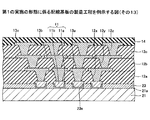
[第1の実施の形態に係る配線基板の構造]
始めに、第1の実施の形態に係る配線基板の構造について説明する。図15は、第1の実施の形態に係る配線基板を例示する断面図である。図15を参照するに、配線基板10は、第1絶縁層12aと、第2絶縁層12bと、第3絶縁層12cと、第1配線層13aと、第2配線層13bと、第3配線層13cと、ソルダーレジスト層14と、接続端子16と、第4金属層17とを有するビルドアップ配線層を備えた配線基板である。
[Structure of Wiring Board According to First Embodiment]
First, the structure of the wiring board according to the first embodiment will be described. FIG. 15 is a cross-sectional view illustrating the wiring board according to the first embodiment. Referring to FIG. 15, the
配線基板10の一方の面10a側には、半導体チップと接続される接続端子として機能する接続端子16が形成されている。接続端子16は、配線基板10の一方の面10aから一部が突出する突出金属層11と、突出金属層11の配線基板10の一方の面10aから突出する部分を覆うように形成されたはんだバンプ15とを有する。突出金属層11は、第2金属層11a及び第3金属層11bを有する。以降、突出金属層11の配線基板10の一方の面10aから突出する部分を便宜上突出部11xと称する場合がある。又、突出部11xの第1絶縁層12aと接する面の反対側の面を面11yと称する場合がある。なお、面11yは、配線基板10上に半導体チップを搭載する際に、突出部11xがはんだを介して半導体チップの電極パッドと接触する部分となる。
A
第1絶縁層12a上(突出部11xの形成面と反対側)には、第1配線層13aが形成されている。更に第1配線層13a及び第1絶縁層12aを覆うように第2絶縁層12bが形成され、第2絶縁層12b上には第2配線層13bが形成されている。更に、第2配線層13b及び第2絶縁層12bを覆うように第3絶縁層12cが形成され、第3絶縁層12c上には第3配線層13cが形成されている。
A
第1配線層13aと突出金属層11を構成する第3金属層11bとは、第1絶縁層12aに形成された第1ビアホール12xを介して電気的に接続されている。第1配線層13aと第2配線層13bとは、第2絶縁層12bに形成された第2ビアホール12yを介して電気的に接続されている。又、第2配線層13bと第3配線層13cとは、第3絶縁層12cに形成された第3ビアホール12zを介して電気的に接続されている。
The
第3配線層13c及び第3絶縁層12cを覆うように、開口部14xを有するソルダーレジスト層14が形成されている。ソルダーレジスト層14の開口部14x内に露出する第3配線層13c上には、第4金属層17が形成されている。第4金属層17は、マザーボード等と接続される電極パッドとして機能する。
A solder resist
配線基板10において、突出部11xは、従来の配線基板の突出金属層(ドーム状等)とは異なり、XZ平面に平行な断面が矩形状である。突出部11xの配線基板10の一方の面10aからの突出量L10は、例えば30〜50μmとすることができる。突出部11xの形状は、例えば円柱状(例えば面11yの直径φ10=φ60〜70μm)とすることができる。突出部11xのピッチP10は、例えば150μmとすることができる。ただし、突出部11xの形状は円柱状には限定されず、柱状であればよい。すなわち、突出部11xの形状は円柱状ではなく、例えば楕円柱状や角柱状(四角柱、六角柱等)であってもよい。なお、本願において、柱状とは、略平行で略同一面積の上面及び下面(底面)を有する立体をいう。
In the
突出金属層11を構成する第2金属層11aの材料としては、例えばAuを用いることができる。又、突出金属層11を構成する第2金属層11aは、突出金属層11を構成する第3金属層11b側からNi層とAu層が積層されたNi/Au層や、Ni層とPd層とAu層が積層されたNi/Pd/Au層等としても構わない。突出金属層11を構成する第3金属層11bの材料としては、例えばCu等を用いることができる。はんだバンプ15の材料としては、例えばPbを含む合金、SnとCuの合金、SnとAgの合金、SnとAgとCuの合金等を用いることができる。
As a material of the
このように、突出部11xはXZ平面に平行な断面が矩形状であるため、アスペクト比(L10/φ10)を高くするが可能となり、狭ピッチ化にも対応可能な接続端子を実現することができる。又、突出部11xはXZ平面に平行な断面が矩形状であるため、半導体チップを実装する際にはんだを介して半導体チップの電極パッドと接触する部分となる面11yの面積を大きくできるため、接続信頼性が高い接続端子を実現することができる。以上が、第1の実施の形態に係る配線基板の構造である。
In this way, since the
[第1の実施の形態に係る配線基板の製造方法]
続いて、第1の実施の形態に係る配線基板の製造方法について説明する。図16〜図30は、第1の実施の形態に係る配線基板の製造工程を例示する図である。図16〜図30において、図15と同一部品については、同一符号を付し、その説明は省略する場合がある。
[Method for Manufacturing Wiring Board According to First Embodiment]
Next, a method for manufacturing a wiring board according to the first embodiment will be described. 16 to 30 are diagrams illustrating the manufacturing process of the wiring board according to the first embodiment. 16 to 30, the same components as those in FIG. 15 are denoted by the same reference numerals, and the description thereof may be omitted.
始めに、図16に示す工程では、支持体21を用意する。なお、21aは支持体21の一方の面を示している。本実施形態では支持体21としてCu箔を用いる。支持体21の厚さは、例えば35〜100μmとすることができる。次いで、図17に示す工程では、支持体21の一方の面21aに、レジスト層22を形成する(実際には、支持体21の一方の面21aと反対側の面もレジスト層で被覆する)。レジスト層22としては、例えば、ドライフィルム等を用いることができる。レジスト層22の厚さは、例えば30〜50μmとすることができる。
First, in the step shown in FIG. 16, a
次いで、図18に示す工程では、レジスト層22に対してパターニング処理を行い、突出金属層11の形成位置に対応する部分のレジスト層22のみを残し、それ以外の部分のレジスト層22を除去する。残ったレジスト層22の形状は、例えば円柱状(例えば断面の直径φ10=φ60〜70μm)とすることができる。ただし、残ったレジスト層22の形状は円柱状には限定されず、柱状であればよい。すなわち、残ったレジスト層22の形状は円柱状ではなく、例えば楕円柱状や角柱状(四角柱、六角柱等)であってもよい。又、残ったレジスト層22のピッチP10は、例えば150μmとすることができる。
Next, in the process shown in FIG. 18, a patterning process is performed on the resist
次いで、図19に示す工程では、支持体21をめっき給電層に利用する電解めっき法等により、支持体21の一方の面21aに第1金属層23を形成する。第1金属層23は、支持体21の一方の面21aのレジスト層22が形成されていない領域に形成される。第1金属層23は、後述する図30に示す工程で支持体21とともにエッチングにより除去されるため、支持体21及び第1金属層23は同一のエッチング液により除去可能な材料により構成されていることが好ましい。具体的には、本実施形態では支持体21としてCu箔を用いているため、第1金属層23の材料はCuであることが好ましい。第1金属層23の厚さT10は、例えば30〜50μmとすることができる。なお、第1金属層23の厚さT10は、突出部11xの配線基板10の一方の面10aからの突出量L10を決定する。すなわち、突出部11xの配線基板10の一方の面10aからの突出量L10は、第1金属層23の厚さT10と略同一となる。
Next, in the step shown in FIG. 19, the
次いで、図20に示す工程では、図19に示すレジスト層22を除去し開口部23xを形成する。これにより、支持体21の一方の面21aに、支持体21の一方の面21aを露出する柱状の貫通孔である開口部23xを有する第1金属層23が形成される。次いで、図21に示す工程では、第1金属層23上にレジスト層24を形成する。レジスト層24には、開口部23xに対応する形状の開口部が形成される。レジスト層24としては、例えば、ドライフィルム等を用いることができる。レジスト層24の厚さは、例えば30〜50μmとすることができる。
Next, in a step shown in FIG. 20, the resist
次いで、図22に示す工程では、支持体21及び第1金属層23をめっき給電層に利用する電解めっき法等により、開口部23xに第2金属層11a及び第3金属層11bをこの順番で積層して突出金属層11を形成する。第2金属層11aは、開口部23xから露出する支持体21の一方の面21a及び開口部23xの内壁面を覆うように形成される。第3金属層11bは、第2金属層11a上に少なくとも開口部23xを完全に充填するように形成される。第2金属層11aの材料としては、例えばAu等を用いることができる。第3金属層11bの材料としては、例えばCu等を用いることができる(図22(a))。
Next, in the step shown in FIG. 22, the
なお、第2金属層11aは、異なる材料からなる複数の金属層が積層された構造を有しても構わない。図22(b)は、異なる材料からなる複数の金属層が積層された構造を有する第2金属層11aの一例である。図22(b)に示す第2金属層11aにおいて、例えば金属層11cをAu層(例えば層厚≒1μm)、金属層11dをPd層(例えば層厚≒1μm)、金属層11eをNi層(例えば層厚≒5μm)とすることができる。異なる材料からなる複数の金属層が積層された構造を有する第2金属層11aの他の例としては、Au層とNi層とをこの順番で積層したAu/Ni層等を挙げることができる。
The
次いで、図23に示す工程では、図22に示すレジスト層24を除去する。次いで、図24に示す工程では、突出金属層11を構成する第3金属層11bを覆うように第1金属層23上に第1絶縁層12aを形成する。第1絶縁層12aの材料としては、エポキシ系樹脂、ポリイミド系樹脂などの樹脂材を用いることができる。第1絶縁層12aの形成方法の一例としては、第1金属層23上に樹脂フィルムをラミネートした後に、樹脂フィルムをプレス(押圧)し、その後、190℃程度の温度で熱処理して硬化させることにより第1絶縁層12aを得ることができる。
Next, in a step shown in FIG. 23, the resist
次いで、図25に示す工程では、支持体21に形成された第1絶縁層12aに、レーザ加工法等を用いて、突出金属層11を構成する第3金属層11bが露出するように第1絶縁層12aを貫通する第1ビアホール12xを形成する。なお、第1絶縁層12aとして感光性樹脂膜を用い、フォトリソグラフィによりパターニングして第1ビアホール12xを形成する方法を用いてもよいし、スクリーン印刷により開口部が設けられた樹脂膜をパターニングして第1ビアホール12xを形成する方法を用いてもよい。
Next, in the step shown in FIG. 25, the first insulating
次いで、図26に示す工程では、第1絶縁層12a上に、ビアホール12x内に露出した突出金属層11を構成する第3金属層11bと電気的に接続する第1配線層13aを形成する。第1配線層13aの材料としては、例えばCu等を用いることができる。第1配線層13aは、例えばセミアディティブ法により形成される。
Next, in the step shown in FIG. 26, the
第1配線層13aを、セミアディティブ法により形成する例を、より詳しく説明すると、先ず、無電解めっき法又はスパッタ法により、第1ビアホール12x内及び第1絶縁層12a上にCuシード層(図示せず)を形成した後に、第1配線層13aに対応する開口部を備えたレジスト層(図示せず)を形成する。次いで、Cuシード層をめっき給電層に利用した電解めっき法により、レジスト層の開口部にCu層パターン(図示せず)を形成する。
An example in which the
続いて、レジスト層を除去した後に、Cu層パターンをマスクにしてCuシード層をエッチングすることにより、第1配線層13aを得る。なお、第1配線層13aの形成方法としては、上述したセミアディティブ法の他にサブトラクティブ法などの各種の配線形成方法を用いることができる。
Subsequently, after removing the resist layer, the
次いで、図27に示す工程では、上記と同様な工程を繰り返すことにより、第1配線層13a〜第3配線層13c及び第1絶縁層12a〜第3絶縁層12cを積層する。すなわち、第1配線層13a及び第1絶縁層12aを被覆する第2絶縁層12bを形成した後に、第1配線層13a上の第2絶縁層12bの部分に第2ビアホール12yを形成する。
Next, in the step shown in FIG. 27, the
更に、第2絶縁層12b上に、第2ビアホール12yを介して第1配線層13aに接続される第2配線層13bを形成する。第2配線層13bとしては、例えばCu等を用いることができる。第2配線層13bは、例えばセミアディティブ法により形成される。
Further, a
更に、第2配線層13b及び第2絶縁層12bを被覆する第3絶縁層12cを形成した後に、第2配線層13b上の第3絶縁層12cの部分に第3ビアホール12zを形成する。更に、第3絶縁層12c上に、第3ビアホール12zを介して第2配線層13bに接続される第3配線層13cを形成する。第3配線層13cとしては、例えば、Cu等を用いることができる。第3配線層13cは、例えばセミアディティブ法により形成される。
Further, after forming the third insulating
このようにして、支持体21の一方の面21aに所定のビルドアップ配線層が形成される。本実施例では、3層のビルドアップ配線層(第1配線層13a〜第3配線層13c)を形成したが、n層(nは1以上の整数)のビルドアップ配線層を形成してもよい。
In this way, a predetermined buildup wiring layer is formed on one
次いで、図28に示す工程では、第3配線層13cを被覆するように第3絶縁層12c上にソルダーレジストを塗布し、ソルダーレジスト層14を形成する。ソルダーレジスト層14の材料としては、例えばエポキシ系樹脂やイミド系樹脂等を含む感光性樹脂組成物を用いることができる。
28, a solder resist is applied on the third insulating
次いで、図29に示す工程では、ソルダーレジスト層14を露光、現像することで開口部14xを形成する。これにより、第3配線層13cの一部は、ソルダーレジスト層14の開口部14x内に露出する。更に、ソルダーレジスト層14の開口部14x内に露出する第3配線層13c上に、例えば無電解めっき法により第4金属層17を形成する。第4金属層17は、マザーボード等と接続される電極パッドとして機能する。
Next, in a step shown in FIG. 29, the
第4金属層17の例としては、Au層、Ni層/Au層をこの順番で積層したNi/Au層、Ni層/Pd層/Au層をこの順番で積層したNi/Pd/Au層等を挙げることができる。又、第4金属層17に代えて、ソルダーレジスト層14の開口部14x内に露出する第3配線層13c上にOSP(Organic Solderability Preservative)処理を施しても構わない。
Examples of the
次いで、図30に示す工程では、図29に示す支持体21及び第1金属層23を除去し、突出金属層11(第2金属層11a及び第3金属層11b)の少なくとも一部を第1絶縁層12aから突出させ柱状の突出部11xを形成する。ここで突出部11xの突出量L10は図19に示す第1金属層23の厚さT10に対応し、例えば30〜50μmとなる。
Next, in the step shown in FIG. 30, the
支持体21及び第1金属層23の材料として何れもCuを選定した場合には、支持体21及び第1金属層23は同一のエッチング液により除去可能である。例えば、支持体21及び第1金属層23は、塩化第二鉄水溶液、塩化第二銅水溶液又は過硫酸アンモニウム水溶液等を用いたウエットエッチングにより除去することができる。この際、突出金属層11の第2金属層11aはCu以外の材料(例えばAu等)から構成されているため、第2金属層11aに対し、支持体21及び第1金属層23を選択的にエッチングして除去することができる。
When Cu is selected as the material of the
次いで、突出金属層11の突出部11xを覆うように、はんだバンプ15を形成することにより、図15に示す配線基板10が製造される。はんだバンプ15は、例えば突出金属層11の突出部11xを覆うように、はんだペーストを印刷し、リフローすることにより形成することができる。はんだバンプ15の材料としては、例えばPbを含む合金、SnとCuの合金、SnとAgの合金、SnとAgとCuの合金等を用いることができる。突出金属層11及びはんだバンプ15は接続端子16を構成し、接続端子16は半導体チップと接続される接続端子として機能する。
Next, by forming the
なお、はんだバンプ15は、配線基板10に必ずしも形成しなくても構わない。例えば配線基板10に搭載する半導体チップの電極パッドにはんだバンプを形成し、半導体チップに形成されたはんだバンプと配線基板10の突出金属層11の突出部11xとを電気的に接続することも可能である。以上が、第1の実施の形態に係る配線基板の製造方法である。
Note that the solder bumps 15 are not necessarily formed on the
このように、第1の実施の形態によれば、突出金属層形成用の開口部を、従来のようにエッチング法により形成せずに、めっき法により形成するため、突出金属層の配線基板の一方の面から突出する部分(突出部)の形状を柱状とすることができる(突出部の断面はドーム状ではなく矩形状となる)。その結果、突出金属層の突出部のアスペクト比を高くするが可能となり、狭ピッチ化にも対応可能な接続端子を実現することができる。又、突出金属層の突出部において、半導体チップを実装する際にはんだを介して半導体チップの電極パッドと接触する部分の面積を大きくできるため、接続信頼性が高い接続端子を実現することができる。 As described above, according to the first embodiment, since the opening for forming the protruding metal layer is not formed by the etching method as in the prior art but is formed by the plating method, the wiring substrate of the protruding metal layer is formed. The shape of the portion protruding from one surface (protruding portion) can be a columnar shape (the cross section of the protruding portion is not a dome shape but a rectangular shape). As a result, the aspect ratio of the protruding portion of the protruding metal layer can be increased, and a connection terminal that can cope with a narrow pitch can be realized. In addition, since the area of the protruding portion of the protruding metal layer that contacts the electrode pad of the semiconductor chip via the solder when mounting the semiconductor chip can be increased, a connection terminal with high connection reliability can be realized. .
〈第2の実施の形態〉
第2の実施の形態では、本発明を多層配線層(ビルドアップ配線層)を有する配線基板に適用する他の例を示す。第2の実施の形態において、第1の実施の形態と共通する部分についてはその説明を省略し、第1の実施の形態と異なる部分を中心に説明する。
<Second Embodiment>
The second embodiment shows another example in which the present invention is applied to a wiring board having a multilayer wiring layer (build-up wiring layer). In the second embodiment, description of parts common to the first embodiment is omitted, and parts different from the first embodiment are mainly described.
[第2の実施の形態に係る配線基板の構造]
始めに、第2の実施の形態に係る配線基板の構造について説明する。図31は、第2の実施の形態に係る配線基板を例示する断面図である。図31を参照するに、配線基板30は、第1絶縁層12aと、第2絶縁層12bと、第3絶縁層12cと、第1配線層13aと、第2配線層13bと、第3配線層13cと、ソルダーレジスト層14と、接続端子36と、第4金属層17とを有するビルドアップ配線層を備えた配線基板である。
[Structure of Wiring Board According to Second Embodiment]
First, the structure of the wiring board according to the second embodiment will be described. FIG. 31 is a cross-sectional view illustrating a wiring board according to the second embodiment. Referring to FIG. 31, the
配線基板30の一方の面30aには、半導体チップと接続される接続端子として機能する接続端子36が形成されている。接続端子36は、配線基板30の一方の面30aから突出する突出金属層31と、突出金属層31を覆うように形成されたはんだバンプ35とを有する。第1配線層13aと突出金属層31とは、第1絶縁層12aに形成された第1ビアホール12xを介して電気的に接続されている。以降、突出金属層31の配線基板30の一方の面30aから突出する部分を便宜上突出部31xと称する場合がある。又、突出部31xの第1絶縁層12aに接する面の反対側の面を面31yと称する場合がある。なお、面31yは、配線基板30上に半導体チップを搭載する際に、突出部31xがはんだを介して半導体チップの電極パッドと接触する部分となる。
A
配線基板30において、突出部31xは、従来の配線基板の突出金属層(ドーム状等)とは異なり、XZ平面に平行な断面が矩形状である。突出部31xの配線基板30の一方の面30aからの突出量L30は、例えば30〜50μmとすることができる。突出部31xの形状は、例えば円柱状(例えば面31yの直径φ30=φ60〜70μm)とすることができる。突出部31xのピッチP30は、例えば150μmとすることができる。ただし、突出部31xの形状は円柱状には限定されず、柱状であればよい。すなわち、突出部31xの形状は円柱状ではなく、例えば楕円柱状や角柱状(四角柱、六角柱等)であってもよい。
In the
突出金属層31の材料としては、例えばCu等を用いることができる。はんだバンプ35の材料としては、例えばPbを含む合金、SnとCuの合金、SnとAgの合金、SnとAgとCuの合金等を用いることができる。
As a material of the protruding
このように、突出部31xはXZ平面に平行な断面が矩形状であるため、アスペクト比(L30/φ30)を高くするが可能となり、狭ピッチ化にも対応可能な接続端子を実現することができる。又、突出部31xはXZ平面に平行な断面が矩形状であるため、半導体チップを実装する際にはんだを介して半導体チップの電極パッドと接触する部分となる面31yの面積を大きくできるため、接続信頼性が高い接続端子を実現することができる。以上が、第2の実施の形態に係る配線基板の構造である。
Thus, since the
[第2の実施の形態に係る配線基板の製造方法]
続いて、第2の実施の形態に係る配線基板の製造方法について説明する。図32〜図35は、第2の実施の形態に係る配線基板の製造工程を例示する図である。図32〜図35において、図31と同一部品については、同一符号を付し、その説明は省略する場合がある。
[Manufacturing Method of Wiring Board According to Second Embodiment]
Then, the manufacturing method of the wiring board based on 2nd Embodiment is demonstrated. 32 to 35 are diagrams illustrating the manufacturing process of the wiring board according to the second embodiment. 32 to 35, parts that are the same as those in FIG. 31 are given the same reference numerals, and descriptions thereof may be omitted.
始めに、第1の実施の形態の図16〜図21に示す工程と同一の工程を実行する。次いで、図32に示す工程では、支持体21及び第1金属層23をめっき給電層に利用する電解めっき法等により、開口部23xに第2金属層11a及び突出金属層31をこの順番で積層する。第2金属層11aは、開口部23xから露出する支持体21の一方の面21a及び開口部23xの内壁面を覆うように形成される。突出金属層31は、第2金属層11a上に少なくとも開口部23xを完全に充填するように形成される。
First, the same steps as those shown in FIGS. 16 to 21 of the first embodiment are executed. Next, in the step shown in FIG. 32, the
第2金属層11aは、後述する図34に示す工程において、支持体21及び第1金属層23を除去するエッチング液により除去不可能な材料により構成されている必要がある。又、第2金属層11aは、後述する図35に示す工程において、突出金属層31に対して選択的にエッチングすることが可能な材料により構成されている必要がある。例えば支持体21、第1金属層23、及び突出金属層31の材料としてCuを用いる場合には、第2金属層11aの材料としては、Niを用いることができる。
The
次いで、第1の実施の形態の図23〜図29に示す工程と同一の工程を実行し、図33に示す構造体を作製する。次いで、図34に示す工程では、図33に示す支持体21及び第1金属層23を除去し、第2金属層11a及び突出金属層31の少なくとも一部を第1絶縁層12aから突出させる。ここで第2金属層11a及び突出金属層31の第1絶縁層12aから突出している部分の突出量L31は図19に示す第1金属層23の厚さT10に対応し、例えば30〜50μmとなる。
Next, the same steps as those shown in FIGS. 23 to 29 of the first embodiment are performed to produce the structure shown in FIG. Next, in the step shown in FIG. 34, the
支持体21及び第1金属層23の材料として何れもCuを選定した場合には、支持体21及び第1金属層23は同一のエッチング液により除去可能である。例えば、支持体21及び第1金属層23は、塩化第二鉄水溶液、塩化第二銅水溶液又は過硫酸アンモニウム水溶液等を用いたウエットエッチングにより除去することができる。この際、第2金属層11aは支持体21及び第1金属層23を除去するエッチング液により除去不可能な材料(例えばNi等)により構成されているため、第2金属層11aに対し、支持体21及び第1金属層23を選択的にエッチングして除去することができる。
When Cu is selected as the material of the
次いで、図35に示す工程では、図34に示す第2金属層11aを除去する。この際、第2金属層11aは突出金属層31(例えばCu等)に対して選択的にエッチングすることが可能な材料(例えばNi等)により構成されているため、突出金属層31に対し第2金属層11aのみを選択的にエッチングして除去することができる。これにより、突出金属層31の一部は、第1絶縁層12aから突出する。ここで、第2金属層11aの厚さは数μm程度であるため、突出部31xの突出量L30は図34に示す突出量L31とほぼ等しく例えば30〜50μmとなる。
Next, in a step shown in FIG. 35, the
例えば突出金属層31がCuであり第2金属層11aがNiである場合には、ニッケル剥離剤を用いたウエットエッチングにより第2金属層11aのみを選択的に除去することができる。ニッケル剥離剤としては、例えば、市販のニッケル剥離剤として知られているエバストリップ(荏原ユージライト社製)、メルストリップ(メルテックス社製)、メックリムーバ(メック社製)等を用いることができる。
For example, when the protruding
次いで、突出金属層31を覆うように、はんだバンプ35を形成することにより、図31に示す配線基板30が製造される。はんだバンプ35は、例えば突出金属層31の突出部31xを覆うように、はんだペーストを印刷し、リフローすることにより形成することができる。はんだバンプ35の材料としては、例えばPbを含む合金、SnとCuの合金、SnとAgの合金、SnとAgとCuの合金等を用いることができる。突出金属層31及びはんだバンプ35は接続端子36を構成し、接続端子36は半導体チップと接続される接続端子として機能する。
Next, by forming solder bumps 35 so as to cover the protruding
なお、はんだバンプ35は、配線基板30に必ずしも形成しなくても構わない。例えば配線基板30に搭載する半導体チップの電極パッドにはんだバンプを形成し、半導体チップに形成されたはんだバンプと配線基板30の突出金属層31の突出部31xとを電気的に接続することも可能である。以上が、第2の実施の形態に係る配線基板の製造方法である。
Note that the solder bumps 35 are not necessarily formed on the
このように、第2の実施の形態によれば、突出金属層形成用の開口部を、従来のようにエッチング法により形成せずに、めっき法により形成するため、突出金属層の配線基板の一方の面から突出する部分(突出部)の形状を柱状とすることができる(突出部の断面はドーム状ではなく矩形状となる)。その結果、突出金属層の突出部のアスペクト比を高くするが可能となり、狭ピッチ化にも対応可能な接続端子を実現することができる。又、突出金属層の突出部において、半導体チップを実装する際にはんだを介して半導体チップの電極パッドと接触する部分の面積を大きくできるため、接続信頼性が高い接続端子を実現することができる。 As described above, according to the second embodiment, since the opening for forming the protruding metal layer is formed by the plating method without forming the opening by the etching method as in the prior art, the wiring substrate of the protruding metal layer is formed. The shape of the portion protruding from one surface (protruding portion) can be a columnar shape (the cross section of the protruding portion is not a dome shape but a rectangular shape). As a result, the aspect ratio of the protruding portion of the protruding metal layer can be increased, and a connection terminal that can cope with a narrow pitch can be realized. In addition, since the area of the protruding portion of the protruding metal layer that contacts the electrode pad of the semiconductor chip via the solder when mounting the semiconductor chip can be increased, a connection terminal with high connection reliability can be realized. .
〈第3の実施の形態〉
第3の実施の形態では、本発明を多層配線層(ビルドアップ配線層)を有する配線基板に適用する他の例を示す。第3の実施の形態において、第1の実施の形態と共通する部分についてはその説明を省略し、第1の実施の形態と異なる部分を中心に説明する。
<Third Embodiment>
The third embodiment shows another example in which the present invention is applied to a wiring board having a multilayer wiring layer (build-up wiring layer). In the third embodiment, description of parts common to the first embodiment will be omitted, and parts different from the first embodiment will be mainly described.
[第3の実施の形態に係る配線基板の構造]
始めに、第3の実施の形態に係る配線基板の構造について説明する。図36は、第3の実施の形態に係る配線基板を例示する断面図である。図36を参照するに、配線基板50は、第1絶縁層12aと、第2絶縁層12bと、第3絶縁層12cと、第1配線層13aと、第2配線層13bと、第3配線層13cと、ソルダーレジスト層14と、接続端子56と、第4金属層17とを有するビルドアップ配線層を備えた配線基板である。
[Structure of Wiring Board According to Third Embodiment]
First, the structure of the wiring board according to the third embodiment will be described. FIG. 36 is a cross-sectional view illustrating a wiring board according to the third embodiment. Referring to FIG. 36, the
配線基板50は配線基板10とは異なり、第4金属層17が形成されている側が半導体チップ搭載面となり、第4金属層17は半導体チップと接続される接続端子として機能する。従って、第4金属層17のピッチは搭載される半導体チップの電極パッドのピッチ(例えば150μm)に合わせて形成されている。一方、接続端子56はマザーボード等と接続される接続端子として機能する。従って、接続端子56のピッチP50はマザーボード等の接続端子のピッチに合わせて(第4金属層17のピッチよりも広く)形成されている。
Unlike the
配線基板50の一方の面50aには、接続端子56が形成されている。接続端子56は、配線基板50の一方の面50aから一部が突出する突出金属層51と、突出金属層51の配線基板50の一方の面50aから突出する部分を覆うように形成されたはんだバンプ55とを有する。以降、突出金属層51の配線基板50の一方の面50aから突出する部分を便宜上突出部51xと称する場合がある。又、突出部51xの第1絶縁層12aと接する面の反対側の面を面51yと称する場合がある。なお、面51yは、配線基板50とマザーボード等とを接続する際に、突出部51xがはんだを介してマザーボード等の電極パッドと接触する部分となる。
A
配線基板50において、突出部51xは、従来の配線基板の突出金属層(ドーム状等)とは異なり、XZ平面に平行な断面が矩形状である。突出部51xの配線基板50の一方の面50aからの突出量L50は、例えば30〜50μmとすることができる。突出部51xの形状は、例えば円柱状(例えば面51yの直径φ50=φ100〜200μm)とすることができる。突出部51xのピッチP50は、例えば500μmとすることができる。ただし、突出部51xの形状は円柱状には限定されず、柱状であればよい。すなわち、突出部51xの形状は円柱状ではなく、例えば楕円柱状や角柱状(四角柱、六角柱等)であってもよい。
In the
突出金属層51は、第2金属層51a及び第3金属層51bを有する。第2金属層51aの材料としては、例えばAuを用いることができる。又、第2金属層51aは、第3金属層51b側からNi層とAu層が積層されたNi/Au層や、第3金属層51b側からNi層とPd層とAu層が積層されたNi/Pd/Au層等としても構わない。第3金属層51bの材料としては、例えばCu等を用いることができる。はんだバンプ55の材料としては、例えばPbを含む合金、SnとCuの合金、SnとAgの合金、SnとAgとCuの合金等を用いることができる。
The protruding
配線基板50のその他の部分の構成は配線基板10と同一であるため、その説明は省略する。又、配線基板50の製造方法は配線基板10の製造方法と同一であるため、その説明は省略する。
Since the configuration of the other parts of the
このように、第3の実施の形態によれば、突出金属層形成用の開口部を、従来のようにエッチング法により形成せずに、めっき法により形成するため、突出金属層の配線基板の一方の面から突出する部分(突出部)の形状を柱状とすることができる(突出部の断面はドーム状ではなく矩形状となる)。その結果、突出金属層において、マザーボード等と接続する際にはんだを介してマザーボード等の接続端子と接触する部分の面積を大きくできるため、接続信頼性が高い接続端子を実現することができる。 As described above, according to the third embodiment, the opening for forming the protruding metal layer is formed by the plating method without forming the opening by the etching method as in the prior art. The shape of the portion protruding from one surface (protruding portion) can be a columnar shape (the cross section of the protruding portion is not a dome shape but a rectangular shape). As a result, in the protruding metal layer, the area of the portion that contacts the connection terminal of the mother board or the like via solder when connecting to the mother board or the like can be increased, so that a connection terminal with high connection reliability can be realized.
〈第4の実施の形態〉
第4の実施の形態では、本発明を多層配線層(ビルドアップ配線層)を有する配線基板に適用する他の例を示す。第4の実施の形態において、第2の実施の形態と共通する部分についてはその説明を省略し、第2の実施の形態と異なる部分を中心に説明する。
<Fourth embodiment>
The fourth embodiment shows another example in which the present invention is applied to a wiring board having a multilayer wiring layer (build-up wiring layer). In the fourth embodiment, description of parts common to the second embodiment is omitted, and parts different from the second embodiment will be mainly described.
[第4の実施の形態に係る配線基板の構造]
始めに、第4の実施の形態に係る配線基板の構造について説明する。図37は、第4の実施の形態に係る配線基板を例示する断面図である。図37を参照するに、配線基板60は、第1絶縁層12aと、第2絶縁層12bと、第3絶縁層12cと、第1配線層13aと、第2配線層13bと、第3配線層13cと、ソルダーレジスト層14と、接続端子66と、第4金属層17とを有するビルドアップ配線層を備えた配線基板である。
[Structure of Wiring Board According to Fourth Embodiment]
First, the structure of the wiring board according to the fourth embodiment will be described. FIG. 37 is a cross-sectional view illustrating a wiring board according to the fourth embodiment. Referring to FIG. 37, the
配線基板60は配線基板30とは異なり、第4金属層17が形成されている側が半導体チップ搭載面となり、第4金属層17は半導体チップと接続される接続端子として機能する。従って、第4金属層17のピッチは搭載される半導体チップの電極パッドのピッチ(例えば150μm)に合わせて形成されている。一方、接続端子66はマザーボード等と接続される接続端子として機能する。従って、接続端子66のピッチP60はマザーボード等の接続端子のピッチに合わせて(第4金属層17のピッチよりも広く)形成されている。
Unlike the
配線基板60の一方の面60aには、接続端子66が形成されている。接続端子66は、配線基板60の一方の面60aから一部が突出する突出金属層61と、突出金属層61の配線基板60の一方の面60aから突出する部分を覆うように形成されたはんだバンプ65とを有する。以降、突出金属層61の配線基板60の一方の面60aから突出する部分を便宜上突出部61xと称する場合がある。又、突出部61xの第1絶縁層12aと接する面の反対側の面を面61yと称する場合がある。なお、面61yは、配線基板60とマザーボード等とを接続する際に、突出部61xがはんだを介してマザーボード等の電極パッドと接触する部分となる。
A
配線基板60において、突出部61xは、従来の配線基板の突出金属層(ドーム状等)とは異なり、XZ平面に平行な断面が矩形状である。突出部61xの配線基板60の一方の面60aからの突出量L60は、例えば30〜50μmとすることができる。突出部61xの形状は、例えば円柱状(例えば面61yの直径φ60=φ100〜200μm)とすることができる。突出部61xのピッチP60は、例えば500μmとすることができる。ただし、突出部61xの形状は円柱状には限定されず、柱状であればよい。すなわち、突出部61xの形状は円柱状ではなく、例えば楕円柱状や角柱状(四角柱、六角柱等)であってもよい。
In the
突出金属層61の材料としては、例えばCu等を用いることができる。はんだバンプ65の材料としては、例えばPbを含む合金、SnとCuの合金、SnとAgの合金、SnとAgとCuの合金等を用いることができる。
As a material of the protruding
配線基板60のその他の部分の構成は配線基板30と同一であるため、その説明は省略する。又、配線基板60の製造方法は配線基板30の製造方法と同一であるため、その説明は省略する。
Since the structure of the other part of the
このように、第4の実施の形態によれば、突出金属層形成用の開口部を、従来のようにエッチング法により形成せずに、めっき法により形成するため、突出金属層の配線基板の一方の面から突出する部分(突出部)の形状を柱状とすることができる(突出部の断面はドーム状ではなく矩形状となる)。その結果、突出金属層において、マザーボード等と接続する際にはんだを介してマザーボード等の接続端子と接触する部分の面積を大きくできるため、接続信頼性が高い接続端子を実現することができる。 As described above, according to the fourth embodiment, since the opening for forming the protruding metal layer is formed by the plating method without being formed by the etching method as in the prior art, the wiring substrate of the protruding metal layer is formed. The shape of the portion protruding from one surface (protruding portion) can be a columnar shape (the cross section of the protruding portion is not a dome shape but a rectangular shape). As a result, in the protruding metal layer, the area of the portion that contacts the connection terminal of the mother board or the like via solder when connecting to the mother board or the like can be increased, so that a connection terminal with high connection reliability can be realized.
〈第5の実施の形態〉
第5の実施の形態では、本発明をビルドアップ配線層を有する配線基板に半導体チップを搭載した半導体パッケージに適用する例を示す。第5の実施の形態において、第1の実施の形態と共通する部分についてはその説明を省略し、第1の実施の形態と異なる部分を中心に説明する。
<Fifth embodiment>
The fifth embodiment shows an example in which the present invention is applied to a semiconductor package in which a semiconductor chip is mounted on a wiring board having a build-up wiring layer. In the fifth embodiment, description of portions common to the first embodiment is omitted, and portions different from the first embodiment are mainly described.
[第5の実施の形態に係る半導体パッケージの構造]
始めに、第5の実施の形態に係る半導体パッケージの構造について説明する。 図38は、第5の実施の形態に係る半導体パッケージを例示する断面図である。図38において、図15と同一部品については、同一符号を付し、その説明は省略する場合がある。図38を参照するに、半導体パッケージ70は、図15に示す配線基板10と、半導体チップ71と、アンダーフィル樹脂75とを有する。
[Structure of Semiconductor Package According to Fifth Embodiment]
First, the structure of the semiconductor package according to the fifth embodiment will be described. FIG. 38 is a cross-sectional view illustrating a semiconductor package according to the fifth embodiment. 38, the same components as those in FIG. 15 are denoted by the same reference numerals, and the description thereof may be omitted. Referring to FIG. 38, the
半導体チップ71は、本体72と、電極パッド73とを有する。本体72は、シリコン等からなる薄板化された半導体基板(図示せず)上に半導体集積回路(図示せず)等が形成されたものである。本体72には、電極パッド73が形成されている。電極パッド73は、半導体集積回路(図示せず)と電気的に接続されている。電極パッド73の材料としては、例えばAu等を用いることができる。配線基板10のはんだバンプ15は、溶融して半導体チップ71の電極パッド73と電気的に接続されている。半導体チップ71と配線基板10の一方の面10aとの間には、アンダーフィル樹脂75が充填されている。
The
配線基板10の突出部11xの断面は矩形状であるため、溶融したはんだバンプ15の一部を介して電極パッド73と対向する部分である面11yの面積を大きくすることが可能となり、接続信頼性が高い接続端子を実現することができる。以上が、第5の実施の形態に係る半導体パッケージの構造である。
Since the cross section of the protruding
[第5の実施の形態に係る半導体パッケージの製造方法]
続いて、第5の実施の形態に係る半導体パッケージの製造方法について説明する。図39及び図40は、第5の実施の形態に係る半導体パッケージの製造工程を例示する図である。図39及び図40において、図38と同一部品については、同一符号を付し、その説明は省略する場合がある。
[Method of Manufacturing Semiconductor Package According to Fifth Embodiment]
Next, a method for manufacturing a semiconductor package according to the fifth embodiment will be described. FIG. 39 and FIG. 40 are diagrams illustrating the manufacturing process of the semiconductor package according to the fifth embodiment. 39 and 40, the same components as those in FIG. 38 are denoted by the same reference numerals, and the description thereof may be omitted.
始めに、図15に示す配線基板10を用意する。次いで、図39に示す工程では、配線基板10の接続端子16が形成されている側と半導体チップ71の電極パッド73が形成されている側とを対向させて、接続端子16と電極パッド73とが対応する位置に来るように配置する。
First, the
次いで、図40に示す工程では、接続端子16を構成するはんだバンプ15を例えば230℃に加熱し、はんだを融解させることにより、接続端子16を構成する突出金属層11と電極パッド73とを電気的に接続する。なお、電極パッド73上にはんだが形成されている場合には、電極パッド73上のはんだとはんだバンプ15とが溶融して合金となり、1つのバンプが形成される。次いで、半導体チップ71と配線基板10の一方の面10aとの間にアンダーフィル樹脂75を充填することにより、図38に示す半導体パッケージ70が完成する。
Next, in the step shown in FIG. 40, the
このように、第5の実施の形態によれば、配線基板に接続端子を介して半導体チップを搭載した半導体パッケージを製造する。この際、配線基板の接続端子は柱状の突出部(突出部の断面はドーム状ではなく矩形状となる)を有する。その結果、突出部のはんだを介して半導体チップの電極パッドと接触する部分の面積を大きくできるため、半導体パッケージにおける配線基板と半導体チップとの接続信頼性を向上することができる。 As described above, according to the fifth embodiment, a semiconductor package in which a semiconductor chip is mounted on a wiring board via a connection terminal is manufactured. At this time, the connection terminal of the wiring board has a columnar protrusion (the cross section of the protrusion is rectangular rather than dome-shaped). As a result, the area of the portion that contacts the electrode pad of the semiconductor chip via the solder of the protruding portion can be increased, so that the connection reliability between the wiring board and the semiconductor chip in the semiconductor package can be improved.
〈第6の実施の形態〉
第6の実施の形態では、本発明をビルドアップ配線層を有する配線基板に半導体チップを搭載した半導体パッケージに適用する他の例を示す。第6の実施の形態において、第2の実施の形態と共通する部分についてはその説明を省略し、第2の実施の形態と異なる部分を中心に説明する。
<Sixth embodiment>
The sixth embodiment shows another example in which the present invention is applied to a semiconductor package in which a semiconductor chip is mounted on a wiring board having a build-up wiring layer. In the sixth embodiment, description of parts common to the second embodiment is omitted, and parts different from the second embodiment are mainly described.
[第6の実施の形態に係る半導体パッケージの構造]
始めに、第6の実施の形態に係る半導体パッケージの構造について説明する。 図41は、第6の実施の形態に係る半導体パッケージを例示する断面図である。図41において、図31と同一部品については、同一符号を付し、その説明は省略する場合がある。図41を参照するに、半導体パッケージ80は、図31に示す配線基板30と、半導体チップ71と、アンダーフィル樹脂75とを有する。
[Structure of Semiconductor Package According to Sixth Embodiment]
First, the structure of the semiconductor package according to the sixth embodiment will be described. FIG. 41 is a cross-sectional view illustrating a semiconductor package according to the sixth embodiment. 41, parts that are the same as the parts shown in FIG. 31 are given the same reference numerals, and explanation thereof is omitted. Referring to FIG. 41, the
半導体チップ71は、本体72と、電極パッド73とを有する。本体72は、シリコン等からなる薄板化された半導体基板(図示せず)上に半導体集積回路(図示せず)等が形成されたものである。本体72には、電極パッド73が形成されている。電極パッド73は、半導体集積回路(図示せず)と電気的に接続されている。電極パッド73の材料としては、例えばAu等を用いることができる。配線基板30のはんだバンプ35は、溶融して半導体チップ71の電極パッド73と電気的に接続されている。半導体チップ71と配線基板30の一方の面30aとの間には、アンダーフィル樹脂75が充填されている。
The
配線基板30の突出部31xの断面は矩形状であるため、溶融したはんだバンプ35の一部を介して電極パッド73と対向する部分である面31yの面積を大きくすることが可能となり、接続信頼性が高い接続端子を実現することができる。以上が、第6の実施の形態に係る半導体パッケージの構造である。なお、第6の実施の形態に係る半導体パッケージの製造方法については、第5の実施の形態に係る半導体パッケージの製造方法と同様であるため、その説明は省略する。
Since the cross section of the protruding
このように、第6の実施の形態によれば、配線基板に接続端子を介して半導体チップを搭載した半導体パッケージを製造する。この際、配線基板の接続端子は柱状の突出部(突出部の断面はドーム状ではなく矩形状となる)を有する。その結果、突出部のはんだを介して半導体チップの電極パッドと接触する部分の面積を大きくできるため、半導体パッケージにおける配線基板と半導体チップとの接続信頼性を向上することができる。 Thus, according to the sixth embodiment, a semiconductor package in which a semiconductor chip is mounted on a wiring board via a connection terminal is manufactured. At this time, the connection terminal of the wiring board has a columnar protrusion (the cross section of the protrusion is rectangular rather than dome-shaped). As a result, the area of the portion that contacts the electrode pad of the semiconductor chip via the solder of the protruding portion can be increased, so that the connection reliability between the wiring board and the semiconductor chip in the semiconductor package can be improved.
以上、好ましい実施の形態について詳説したが、上述した実施の形態に制限されることはなく、特許請求の範囲に記載された範囲を逸脱することなく、上述した実施の形態に種々の変形及び置換を加えることができる。 The preferred embodiment has been described in detail above. However, the present invention is not limited to the above-described embodiment, and various modifications and replacements are made to the above-described embodiment without departing from the scope described in the claims. Can be added.
例えば、各実施の形態において、各配線層をセミアディティブ法で形成する例を示したが、各配線層は、セミアディティブ法の他にサブトラクティブ法等の各種の方法を用いて形成することができる。 For example, in each embodiment, an example in which each wiring layer is formed by a semi-additive method has been described. However, each wiring layer can be formed by using various methods such as a subtractive method in addition to the semi-additive method. it can.
10、30、50、60 配線基板
10a、30a、50a、60a 配線基板の一方の面
11、31、51、61 突出金属層
11a、51a 第2金属層
11b、51b 第3金属層
11x、31x、51x、61x 突出部
12a 第1絶縁層
12b 第2絶縁層
12c 第3絶縁層
12x 第1ビアホール
12y 第2ビアホール
12z 第3ビアホール
13a 第1配線層
13b 第2配線層
13c 第3配線層
14 ソルダーレジスト層
14x 開口部
15、35、55、65 はんだバンプ
16、36、56、66 接続端子
17 第4金属層
21 支持体
21a 支持体の一方の面
22、24 レジスト層
23 第1金属層
70、80 半導体パッケージ
71 半導体チップ
72 本体
73 電極パッド
75 アンダーフィル樹脂
L10、L30、L50、L60 突出量
P10、P30、P50、P60 ピッチ
T10 厚さ
φ10、φ30、φ50、φ60 直径
10, 30, 50, 60
Claims (18)
前記柱状の貫通孔から露出する前記支持体の表面及び前記柱状の貫通孔の内壁面を覆うように第2金属層を形成する第2金属層形成工程と、
前記第2金属層上に前記柱状の貫通孔を充填するように第3金属層を形成する第3金属層形成工程と、
前記第3金属層を覆うように前記第1金属層上に絶縁層を形成する絶縁層形成工程と、
前記絶縁層の一方の面に、前記第3金属層と電気的に接続する配線層を形成する配線層形成工程と、
前記支持体及び前記第1金属層を除去し、前記第2金属層及び前記第3金属層を含んで構成され前記絶縁層の他方の面から突出する突出部を形成する突出部形成工程(1)と、を有する配線基板の製造方法。 A first metal layer forming step of forming a first metal layer having a columnar through hole exposing the surface of the support on the support;
A second metal layer forming step of forming a second metal layer so as to cover the surface of the support exposed from the columnar through hole and the inner wall surface of the columnar through hole;
A third metal layer forming step of forming a third metal layer so as to fill the columnar through-holes on the second metal layer;
An insulating layer forming step of forming an insulating layer on the first metal layer so as to cover the third metal layer;
A wiring layer forming step of forming a wiring layer electrically connected to the third metal layer on one surface of the insulating layer;
A projecting portion forming step (1) of removing the support and the first metal layer and forming a projecting portion that includes the second metal layer and the third metal layer and projects from the other surface of the insulating layer. And a method of manufacturing a wiring board.
前記支持体上に前記柱状の貫通孔に対応する柱状のレジスト層を形成する第1工程と、
前記支持体上の前記柱状のレジスト層が形成されていない領域に前記第1金属層を形成する第2工程と、
前記柱状のレジスト層を除去する第3工程と、を有する請求項1乃至3の何れか一項記載の配線基板の製造方法。 The first metal layer forming step includes:
A first step of forming a columnar resist layer corresponding to the columnar through-hole on the support;
A second step of forming the first metal layer in a region where the columnar resist layer is not formed on the support;
A method for manufacturing a wiring board according to claim 1, further comprising a third step of removing the columnar resist layer.
前記絶縁層の一方の面に、前記第3金属層を露出するビアホールを形成する工程と、 Forming a via hole that exposes the third metal layer on one surface of the insulating layer;
前記絶縁層の一方の面上に、前記ビアホールを介して前記第3金属層に接続された配線層を形成する工程と、を有する請求項1乃至10の何れか一項記載の配線基板の製造方法。 Forming a wiring layer connected to the third metal layer through the via hole on one surface of the insulating layer. 11. Manufacturing of a wiring board according to claim 1. Method.
前記突出部と前記電極パッドとを対向させるように、前記配線基板上に前記半導体チップを配置する配置工程と、
前記突出部と前記電極パッドとを電気的に接続する接続工程と、を有する半導体パッケージの製造方法。 A preparation step of preparing a wiring board having a protruding portion manufactured by the manufacturing method according to any one of claims 1 to 16 , and a semiconductor chip having an electrode pad;
An arrangement step of arranging the semiconductor chip on the wiring board so that the protruding portion and the electrode pad are opposed to each other;
A method of manufacturing a semiconductor package, comprising: a connecting step of electrically connecting the protruding portion and the electrode pad.
Priority Applications (6)
| Application Number | Priority Date | Filing Date | Title |
|---|---|---|---|
| JP2009099989A JP5147779B2 (en) | 2009-04-16 | 2009-04-16 | Wiring board manufacturing method and semiconductor package manufacturing method |
| US12/755,555 US8458900B2 (en) | 2009-04-16 | 2010-04-07 | Wiring substrate having columnar protruding part |
| TW99111229A TWI472283B (en) | 2009-04-16 | 2010-04-12 | Wiring substrate having columnar protruding part |
| KR1020100034673A KR101709629B1 (en) | 2009-04-16 | 2010-04-15 | Method for manufacturing wiring substrate having columnar protruding part |
| US13/892,416 US9018538B2 (en) | 2009-04-16 | 2013-05-13 | Wiring substrate having columnar protruding part |
| US14/673,981 US20150206833A1 (en) | 2009-04-16 | 2015-03-31 | Wiring substrate having columnar protruding part |
Applications Claiming Priority (1)
| Application Number | Priority Date | Filing Date | Title |
|---|---|---|---|
| JP2009099989A JP5147779B2 (en) | 2009-04-16 | 2009-04-16 | Wiring board manufacturing method and semiconductor package manufacturing method |
Related Child Applications (1)
| Application Number | Title | Priority Date | Filing Date |
|---|---|---|---|
| JP2012222420A Division JP5422718B2 (en) | 2012-10-04 | 2012-10-04 | Wiring board and semiconductor package |
Publications (3)
| Publication Number | Publication Date |
|---|---|
| JP2010251552A JP2010251552A (en) | 2010-11-04 |
| JP2010251552A5 JP2010251552A5 (en) | 2012-05-10 |
| JP5147779B2 true JP5147779B2 (en) | 2013-02-20 |
Family
ID=42980152
Family Applications (1)
| Application Number | Title | Priority Date | Filing Date |
|---|---|---|---|
| JP2009099989A Active JP5147779B2 (en) | 2009-04-16 | 2009-04-16 | Wiring board manufacturing method and semiconductor package manufacturing method |
Country Status (4)
| Country | Link |
|---|---|
| US (3) | US8458900B2 (en) |
| JP (1) | JP5147779B2 (en) |
| KR (1) | KR101709629B1 (en) |
| TW (1) | TWI472283B (en) |
Families Citing this family (53)
| Publication number | Priority date | Publication date | Assignee | Title |
|---|---|---|---|---|
| JP5147779B2 (en) * | 2009-04-16 | 2013-02-20 | 新光電気工業株式会社 | Wiring board manufacturing method and semiconductor package manufacturing method |
| US8698303B2 (en) * | 2010-11-23 | 2014-04-15 | Ibiden Co., Ltd. | Substrate for mounting semiconductor, semiconductor device and method for manufacturing semiconductor device |
| TWI454320B (en) * | 2011-08-19 | 2014-10-01 | Jieng Tai Internat Electric Corp | Method of filling throught hole |
| JP5861400B2 (en) * | 2011-11-09 | 2016-02-16 | イビデン株式会社 | Semiconductor mounting materials |
| KR101287742B1 (en) * | 2011-11-23 | 2013-07-18 | 삼성전기주식회사 | Printed circuit board and manufacturing method thereof |
| JP5886617B2 (en) * | 2011-12-02 | 2016-03-16 | 新光電気工業株式会社 | Wiring substrate, manufacturing method thereof, and semiconductor package |
| JP2013247201A (en) * | 2012-05-24 | 2013-12-09 | Shinko Electric Ind Co Ltd | Wiring board, mounting structure, and method of manufacturing wiring board |
| TWI637467B (en) * | 2012-05-24 | 2018-10-01 | 欣興電子股份有限公司 | Interposed substrate and manufacturing method thereof |
| US9269681B2 (en) * | 2012-11-16 | 2016-02-23 | Qualcomm Incorporated | Surface finish on trace for a thermal compression flip chip (TCFC) |
| US9299649B2 (en) | 2013-02-08 | 2016-03-29 | Taiwan Semiconductor Manufacturing Company, Ltd. | 3D packages and methods for forming the same |
| US8802504B1 (en) * | 2013-03-14 | 2014-08-12 | Taiwan Semiconductor Manufacturing Company, Ltd. | 3D packages and methods for forming the same |
| CN104219867A (en) * | 2013-05-31 | 2014-12-17 | 宏启胜精密电子(秦皇岛)有限公司 | A circuit board and a manufacturing method thereof |
| US8981842B1 (en) * | 2013-10-25 | 2015-03-17 | Taiwan Semiconductor Manufacturing Company Limited | Integrated circuit comprising buffer chain |
| KR20150064976A (en) * | 2013-12-04 | 2015-06-12 | 삼성전기주식회사 | Printed circuit board and manufacturing method thereof |
| US20150195912A1 (en) * | 2014-01-08 | 2015-07-09 | Zhuhai Advanced Chip Carriers & Electronic Substrate Solutions Technologies Co. Ltd. | Substrates With Ultra Fine Pitch Flip Chip Bumps |
| JP6543887B2 (en) * | 2014-02-24 | 2019-07-17 | 日立化成株式会社 | Bumped wiring board and method of manufacturing the same |
| US9693455B1 (en) * | 2014-03-27 | 2017-06-27 | STATS ChipPAC Pte. Ltd. | Integrated circuit packaging system with plated copper posts and method of manufacture thereof |
| US20150279815A1 (en) * | 2014-03-28 | 2015-10-01 | Stats Chippac, Ltd. | Semiconductor Device and Method of Forming Substrate Having Conductive Columns |
| JP2016021496A (en) * | 2014-07-15 | 2016-02-04 | イビデン株式会社 | Wiring board and manufacturing method for the same |
| US10001439B2 (en) * | 2014-08-04 | 2018-06-19 | National Institute Of Advanced Industrial Science And Technology | Localized surface plasmon resonance sensing chip and localized surface plasmon resonance sensing system |
| JP5795415B1 (en) | 2014-08-29 | 2015-10-14 | 新光電気工業株式会社 | Wiring board and manufacturing method thereof |
| TWI562275B (en) * | 2014-11-27 | 2016-12-11 | Advance Process Integrate Technology Ltd | Process of forming waferless interposer |
| US9899248B2 (en) * | 2014-12-03 | 2018-02-20 | Taiwan Semiconductor Manufacturing Company, Ltd. | Method of forming semiconductor packages having through package vias |
| US10325853B2 (en) * | 2014-12-03 | 2019-06-18 | Taiwan Semiconductor Manufacturing Company, Ltd. | Method of forming semiconductor packages having through package vias |
| TWI595810B (en) * | 2015-05-22 | 2017-08-11 | 欣興電子股份有限公司 | Package structure and method for manufacturing the same |
| CN106298707B (en) * | 2015-06-05 | 2019-05-21 | 欣兴电子股份有限公司 | Encapsulating structure and preparation method thereof |
| US9755030B2 (en) | 2015-12-17 | 2017-09-05 | International Business Machines Corporation | Method for reduced source and drain contact to gate stack capacitance |
| KR102077583B1 (en) * | 2016-04-28 | 2020-02-17 | 가부시키가이샤 무라타 세이사쿠쇼 | A seismic device |
| CN107424973B (en) * | 2016-05-23 | 2020-01-21 | 凤凰先驱股份有限公司 | Package substrate and method for fabricating the same |
| JP2018032661A (en) * | 2016-08-22 | 2018-03-01 | イビデン株式会社 | Printed wiring board and method for manufacturing the same |
| CN107872929B (en) * | 2016-09-27 | 2021-02-05 | 欣兴电子股份有限公司 | Circuit board and manufacturing method thereof |
| US9922924B1 (en) * | 2016-11-03 | 2018-03-20 | Micron Technology, Inc. | Interposer and semiconductor package |
| US9922845B1 (en) * | 2016-11-03 | 2018-03-20 | Micron Technology, Inc. | Semiconductor package and fabrication method thereof |
| KR101944997B1 (en) * | 2017-01-06 | 2019-02-01 | 조인셋 주식회사 | Metal pad interface |
| TWI644598B (en) * | 2017-04-21 | 2018-12-11 | 南亞電路板股份有限公司 | Circuit board structure and method for forming the same |
| TWI643532B (en) * | 2017-05-04 | 2018-12-01 | 南亞電路板股份有限公司 | Circuit board structure and method for fabricating the same |
| US10325842B2 (en) * | 2017-09-08 | 2019-06-18 | Advanced Semiconductor Engineering, Inc. | Substrate for packaging a semiconductor device package and a method of manufacturing the same |
| US10515889B2 (en) | 2017-10-13 | 2019-12-24 | Advanced Semiconductor Engineering, Inc. | Semiconductor package device and method of manufacturing the same |
| US10163758B1 (en) * | 2017-10-30 | 2018-12-25 | Taiwan Semiconductor Manufacturing Company Ltd. | Semiconductor structure and manufacturing method for the same |
| JP2019140174A (en) * | 2018-02-07 | 2019-08-22 | イビデン株式会社 | Printed wiring board and method for manufacturing printed wiring board |
| US10573572B2 (en) | 2018-07-19 | 2020-02-25 | Advanced Semiconductor Engineering, Inc. | Electronic device and method for manufacturing a semiconductor package structure |
| KR102530754B1 (en) * | 2018-08-24 | 2023-05-10 | 삼성전자주식회사 | Method for manufacturing semiconductor package having redistribution layer |
| JP7154913B2 (en) * | 2018-09-25 | 2022-10-18 | 株式会社東芝 | Semiconductor device and its manufacturing method |
| US11109481B2 (en) * | 2019-02-15 | 2021-08-31 | Ibiden Co., Ltd. | Method for manufacturing printed wiring board and printed wiring board |
| WO2020203724A1 (en) * | 2019-03-29 | 2020-10-08 | 株式会社村田製作所 | Resin multilayer substrate and method for producing resin multilayer substrate |
| JP2020188209A (en) * | 2019-05-16 | 2020-11-19 | イビデン株式会社 | Printed wiring board and manufacturing method thereof |
| WO2021031125A1 (en) * | 2019-08-20 | 2021-02-25 | 华为技术有限公司 | Circuit-embedded substrate, chip encapsulation structure and manufacturing method for substrate |
| CN112885806B (en) * | 2019-11-29 | 2022-03-08 | 长鑫存储技术有限公司 | Substrate and preparation method thereof, chip packaging structure and packaging method thereof |
| JP2021093417A (en) * | 2019-12-09 | 2021-06-17 | イビデン株式会社 | Print circuit board and manufacturing method of print circuit board |
| JP2021132068A (en) * | 2020-02-18 | 2021-09-09 | イビデン株式会社 | Printed wiring board and manufacturing method of the same |
| KR20220009193A (en) * | 2020-07-15 | 2022-01-24 | 삼성전자주식회사 | Semiconductor pacakge device |
| US20220199427A1 (en) * | 2020-12-23 | 2022-06-23 | Intel Corporation | Multi-step isotropic etch patterning of thick copper layers for forming high aspect-ratio conductors |
| US20220312591A1 (en) * | 2021-03-26 | 2022-09-29 | Juniper Networks, Inc. | Substrate with conductive pads and conductive layers |
Family Cites Families (40)
| Publication number | Priority date | Publication date | Assignee | Title |
|---|---|---|---|---|
| US3968193A (en) * | 1971-08-27 | 1976-07-06 | International Business Machines Corporation | Firing process for forming a multilayer glass-metal module |
| US4240198A (en) * | 1979-02-21 | 1980-12-23 | International Telephone And Telegraph Corporation | Method of making conductive elastomer connector |
| US5054192A (en) * | 1987-05-21 | 1991-10-08 | Cray Computer Corporation | Lead bonding of chips to circuit boards and circuit boards to circuit boards |
| US4847136A (en) * | 1988-03-21 | 1989-07-11 | Hughes Aircraft Company | Thermal expansion mismatch forgivable printed wiring board for ceramic leadless chip carrier |
| US5399898A (en) * | 1992-07-17 | 1995-03-21 | Lsi Logic Corporation | Multi-chip semiconductor arrangements using flip chip dies |
| US5229647A (en) * | 1991-03-27 | 1993-07-20 | Micron Technology, Inc. | High density data storage using stacked wafers |
| US5334804A (en) * | 1992-11-17 | 1994-08-02 | Fujitsu Limited | Wire interconnect structures for connecting an integrated circuit to a substrate |
| JPH08236654A (en) * | 1995-02-23 | 1996-09-13 | Matsushita Electric Ind Co Ltd | Chip carrier and manufacture thereof |
| US6809421B1 (en) * | 1996-12-02 | 2004-10-26 | Kabushiki Kaisha Toshiba | Multichip semiconductor device, chip therefor and method of formation thereof |
| US5900674A (en) * | 1996-12-23 | 1999-05-04 | General Electric Company | Interface structures for electronic devices |
| US6002168A (en) * | 1997-11-25 | 1999-12-14 | Tessera, Inc. | Microelectronic component with rigid interposer |
| US6057600A (en) * | 1997-11-27 | 2000-05-02 | Kyocera Corporation | Structure for mounting a high-frequency package |
| US6054772A (en) * | 1998-04-29 | 2000-04-25 | National Semiconductor Corporation | Chip sized package |
| JP3825181B2 (en) * | 1998-08-20 | 2006-09-20 | 沖電気工業株式会社 | Semiconductor device manufacturing method and semiconductor device |
| US6329713B1 (en) * | 1998-10-21 | 2001-12-11 | International Business Machines Corporation | Integrated circuit chip carrier assembly comprising a stiffener attached to a dielectric substrate |
| IL128200A (en) * | 1999-01-24 | 2003-11-23 | Amitec Advanced Multilayer Int | Chip carrier substrate |
| JP3973340B2 (en) | 1999-10-05 | 2007-09-12 | Necエレクトロニクス株式会社 | Semiconductor device, wiring board, and manufacturing method thereof |
| JP2001144204A (en) * | 1999-11-16 | 2001-05-25 | Nec Corp | Semiconductor device and manufacture thereof |
| JP3629178B2 (en) * | 2000-02-21 | 2005-03-16 | Necエレクトロニクス株式会社 | Flip chip type semiconductor device and manufacturing method thereof |
| US6441479B1 (en) * | 2000-03-02 | 2002-08-27 | Micron Technology, Inc. | System-on-a-chip with multi-layered metallized through-hole interconnection |
| JP3677429B2 (en) * | 2000-03-09 | 2005-08-03 | Necエレクトロニクス株式会社 | Method of manufacturing flip chip type semiconductor device |
| DE10031204A1 (en) * | 2000-06-27 | 2002-01-17 | Infineon Technologies Ag | System carrier for semiconductor chips and electronic components and manufacturing method for a system carrier and for electronic components |
| JP3653452B2 (en) | 2000-07-31 | 2005-05-25 | 株式会社ノース | WIRING CIRCUIT BOARD, ITS MANUFACTURING METHOD, SEMICONDUCTOR INTEGRATED CIRCUIT DEVICE, AND ITS MANUFACTURING METHOD |
| JP2002111185A (en) * | 2000-10-03 | 2002-04-12 | Sony Chem Corp | Wiring circuit board with bumps and method of manufacturing the same |
| JP3546961B2 (en) | 2000-10-18 | 2004-07-28 | 日本電気株式会社 | Wiring board for mounting semiconductor device, method of manufacturing the same, and semiconductor package |
| US6673653B2 (en) * | 2001-02-23 | 2004-01-06 | Eaglestone Partners I, Llc | Wafer-interposer using a ceramic substrate |
| JP3875867B2 (en) * | 2001-10-15 | 2007-01-31 | 新光電気工業株式会社 | Method for forming holes in silicon substrate |
| JP3874669B2 (en) | 2002-01-25 | 2007-01-31 | 日本特殊陶業株式会社 | Wiring board manufacturing method |
| US6908784B1 (en) * | 2002-03-06 | 2005-06-21 | Micron Technology, Inc. | Method for fabricating encapsulated semiconductor components |
| JP4268434B2 (en) * | 2003-04-09 | 2009-05-27 | 大日本印刷株式会社 | Wiring board manufacturing method |
| JP4708148B2 (en) * | 2005-10-07 | 2011-06-22 | ルネサスエレクトロニクス株式会社 | Semiconductor device |
| JP2007165513A (en) * | 2005-12-13 | 2007-06-28 | Shinko Electric Ind Co Ltd | Method of manufacturing multilayered wiring board for semiconductor device, and method of manufacturing semiconductor device |
| KR100782798B1 (en) * | 2006-02-22 | 2007-12-05 | 삼성전기주식회사 | COB Package and Its Manufacturing method |
| JP2008091639A (en) * | 2006-10-02 | 2008-04-17 | Nec Electronics Corp | Electronic equipment, and manufacturing method thereof |
| KR100832651B1 (en) * | 2007-06-20 | 2008-05-27 | 삼성전기주식회사 | Printed circuit board |
| US20090056998A1 (en) * | 2007-08-31 | 2009-03-05 | International Business Machines Corporation | Methods for manufacturing a semi-buried via and articles comprising the same |
| KR100992181B1 (en) * | 2007-12-26 | 2010-11-04 | 삼성전기주식회사 | Packaging board and manufacturing method thereof |
| JP4835629B2 (en) * | 2008-04-11 | 2011-12-14 | 凸版印刷株式会社 | Manufacturing method of semiconductor device |
| KR20100065691A (en) | 2008-12-08 | 2010-06-17 | 삼성전기주식회사 | A printed circuit board comprising a metal bump and a method of manufacturing the same |
| JP5147779B2 (en) * | 2009-04-16 | 2013-02-20 | 新光電気工業株式会社 | Wiring board manufacturing method and semiconductor package manufacturing method |
-
2009
- 2009-04-16 JP JP2009099989A patent/JP5147779B2/en active Active
-
2010
- 2010-04-07 US US12/755,555 patent/US8458900B2/en active Active
- 2010-04-12 TW TW99111229A patent/TWI472283B/en active
- 2010-04-15 KR KR1020100034673A patent/KR101709629B1/en active IP Right Grant
-
2013
- 2013-05-13 US US13/892,416 patent/US9018538B2/en active Active
-
2015
- 2015-03-31 US US14/673,981 patent/US20150206833A1/en not_active Abandoned
Also Published As
| Publication number | Publication date |
|---|---|
| KR20100114845A (en) | 2010-10-26 |
| TWI472283B (en) | 2015-02-01 |
| TW201041472A (en) | 2010-11-16 |
| KR101709629B1 (en) | 2017-02-23 |
| US20150206833A1 (en) | 2015-07-23 |
| JP2010251552A (en) | 2010-11-04 |
| US20130250533A1 (en) | 2013-09-26 |
| US20100263923A1 (en) | 2010-10-21 |
| US9018538B2 (en) | 2015-04-28 |
| US8458900B2 (en) | 2013-06-11 |
Similar Documents
| Publication | Publication Date | Title |
|---|---|---|
| JP5147779B2 (en) | Wiring board manufacturing method and semiconductor package manufacturing method | |
| JP6076653B2 (en) | Electronic component built-in substrate and manufacturing method of electronic component built-in substrate | |
| JP5026400B2 (en) | Wiring board and manufacturing method thereof | |
| JP4619223B2 (en) | Semiconductor package and manufacturing method thereof | |
| JP5221315B2 (en) | Wiring board and manufacturing method thereof | |
| JP5421254B2 (en) | Multi-layer wiring element with pin interface | |
| US7435680B2 (en) | Method of manufacturing a circuit substrate and method of manufacturing an electronic parts packaging structure | |
| US8749073B2 (en) | Wiring board, method of manufacturing the same, and semiconductor device | |
| JP3813402B2 (en) | Manufacturing method of semiconductor device | |
| US20100139962A1 (en) | Wiring board and method of manufacturing the same | |
| JP5951414B2 (en) | Electronic component built-in substrate and manufacturing method of electronic component built-in substrate | |
| JP4769056B2 (en) | Wiring board and method of manufacturing the same | |
| JP2008300507A (en) | Wiring substrate and manufacturing process of the same | |
| JP2000138313A (en) | Semiconductor device and its manufacture | |
| JP2017163027A (en) | Wiring board, semiconductor device, and manufacturing method for wiring board | |
| JP2011014944A (en) | Method of manufacturing electronic parts packaging structure | |
| KR101011339B1 (en) | Process for producing wiring board | |
| JP5422718B2 (en) | Wiring board and semiconductor package | |
| JP5653144B2 (en) | Manufacturing method of semiconductor package | |
| JP2023005616A (en) | wiring board | |
| JP3975887B2 (en) | Film carrier and manufacturing method thereof | |
| JP2018032802A (en) | Wiring board and semiconductor element package structure using the same |
Legal Events
| Date | Code | Title | Description |
|---|---|---|---|
| A521 | Request for written amendment filed |
Free format text: JAPANESE INTERMEDIATE CODE: A523 Effective date: 20120314 |
|
| A621 | Written request for application examination |
Free format text: JAPANESE INTERMEDIATE CODE: A621 Effective date: 20120314 |
|
| A977 | Report on retrieval |
Free format text: JAPANESE INTERMEDIATE CODE: A971007 Effective date: 20120726 |
|
| A131 | Notification of reasons for refusal |
Free format text: JAPANESE INTERMEDIATE CODE: A131 Effective date: 20120807 |
|
| A521 | Request for written amendment filed |
Free format text: JAPANESE INTERMEDIATE CODE: A523 Effective date: 20121004 |
|
| TRDD | Decision of grant or rejection written | ||
| A01 | Written decision to grant a patent or to grant a registration (utility model) |
Free format text: JAPANESE INTERMEDIATE CODE: A01 Effective date: 20121113 |
|
| A61 | First payment of annual fees (during grant procedure) |
Free format text: JAPANESE INTERMEDIATE CODE: A61 Effective date: 20121127 |
|
| R150 | Certificate of patent or registration of utility model |
Ref document number: 5147779 Country of ref document: JP Free format text: JAPANESE INTERMEDIATE CODE: R150 Free format text: JAPANESE INTERMEDIATE CODE: R150 |
|
| FPAY | Renewal fee payment (event date is renewal date of database) |
Free format text: PAYMENT UNTIL: 20151207 Year of fee payment: 3 |