JP5224845B2 - Semiconductor device manufacturing method and semiconductor device - Google Patents
Semiconductor device manufacturing method and semiconductor device Download PDFInfo
- Publication number
- JP5224845B2 JP5224845B2 JP2008036235A JP2008036235A JP5224845B2 JP 5224845 B2 JP5224845 B2 JP 5224845B2 JP 2008036235 A JP2008036235 A JP 2008036235A JP 2008036235 A JP2008036235 A JP 2008036235A JP 5224845 B2 JP5224845 B2 JP 5224845B2
- Authority
- JP
- Japan
- Prior art keywords
- semiconductor device
- metal
- support substrate
- modification
- semiconductor chip
- Prior art date
- Legal status (The legal status is an assumption and is not a legal conclusion. Google has not performed a legal analysis and makes no representation as to the accuracy of the status listed.)
- Active
Links
Images


Classifications
-
- H—ELECTRICITY
- H05—ELECTRIC TECHNIQUES NOT OTHERWISE PROVIDED FOR
- H05K—PRINTED CIRCUITS; CASINGS OR CONSTRUCTIONAL DETAILS OF ELECTRIC APPARATUS; MANUFACTURE OF ASSEMBLAGES OF ELECTRICAL COMPONENTS
- H05K3/00—Apparatus or processes for manufacturing printed circuits
- H05K3/46—Manufacturing multilayer circuits
-
- H—ELECTRICITY
- H01—ELECTRIC ELEMENTS
- H01L—SEMICONDUCTOR DEVICES NOT COVERED BY CLASS H10
- H01L23/00—Details of semiconductor or other solid state devices
- H01L23/52—Arrangements for conducting electric current within the device in operation from one component to another, i.e. interconnections, e.g. wires, lead frames
- H01L23/538—Arrangements for conducting electric current within the device in operation from one component to another, i.e. interconnections, e.g. wires, lead frames the interconnection structure between a plurality of semiconductor chips being formed on, or in, insulating substrates
- H01L23/5389—Arrangements for conducting electric current within the device in operation from one component to another, i.e. interconnections, e.g. wires, lead frames the interconnection structure between a plurality of semiconductor chips being formed on, or in, insulating substrates the chips being integrally enclosed by the interconnect and support structures
-
- H—ELECTRICITY
- H01—ELECTRIC ELEMENTS
- H01L—SEMICONDUCTOR DEVICES NOT COVERED BY CLASS H10
- H01L23/00—Details of semiconductor or other solid state devices
- H01L23/12—Mountings, e.g. non-detachable insulating substrates
-
- H—ELECTRICITY
- H01—ELECTRIC ELEMENTS
- H01L—SEMICONDUCTOR DEVICES NOT COVERED BY CLASS H10
- H01L24/00—Arrangements for connecting or disconnecting semiconductor or solid-state bodies; Methods or apparatus related thereto
- H01L24/93—Batch processes
- H01L24/95—Batch processes at chip-level, i.e. with connecting carried out on a plurality of singulated devices, i.e. on diced chips
- H01L24/97—Batch processes at chip-level, i.e. with connecting carried out on a plurality of singulated devices, i.e. on diced chips the devices being connected to a common substrate, e.g. interposer, said common substrate being separable into individual assemblies after connecting
-
- H—ELECTRICITY
- H01—ELECTRIC ELEMENTS
- H01L—SEMICONDUCTOR DEVICES NOT COVERED BY CLASS H10
- H01L2224/00—Indexing scheme for arrangements for connecting or disconnecting semiconductor or solid-state bodies and methods related thereto as covered by H01L24/00
- H01L2224/01—Means for bonding being attached to, or being formed on, the surface to be connected, e.g. chip-to-package, die-attach, "first-level" interconnects; Manufacturing methods related thereto
- H01L2224/02—Bonding areas; Manufacturing methods related thereto
- H01L2224/04—Structure, shape, material or disposition of the bonding areas prior to the connecting process
- H01L2224/0401—Bonding areas specifically adapted for bump connectors, e.g. under bump metallisation [UBM]
-
- H—ELECTRICITY
- H01—ELECTRIC ELEMENTS
- H01L—SEMICONDUCTOR DEVICES NOT COVERED BY CLASS H10
- H01L2224/00—Indexing scheme for arrangements for connecting or disconnecting semiconductor or solid-state bodies and methods related thereto as covered by H01L24/00
- H01L2224/01—Means for bonding being attached to, or being formed on, the surface to be connected, e.g. chip-to-package, die-attach, "first-level" interconnects; Manufacturing methods related thereto
- H01L2224/02—Bonding areas; Manufacturing methods related thereto
- H01L2224/04—Structure, shape, material or disposition of the bonding areas prior to the connecting process
- H01L2224/04105—Bonding areas formed on an encapsulation of the semiconductor or solid-state body, e.g. bonding areas on chip-scale packages
-
- H—ELECTRICITY
- H01—ELECTRIC ELEMENTS
- H01L—SEMICONDUCTOR DEVICES NOT COVERED BY CLASS H10
- H01L2224/00—Indexing scheme for arrangements for connecting or disconnecting semiconductor or solid-state bodies and methods related thereto as covered by H01L24/00
- H01L2224/01—Means for bonding being attached to, or being formed on, the surface to be connected, e.g. chip-to-package, die-attach, "first-level" interconnects; Manufacturing methods related thereto
- H01L2224/10—Bump connectors; Manufacturing methods related thereto
- H01L2224/12—Structure, shape, material or disposition of the bump connectors prior to the connecting process
- H01L2224/12105—Bump connectors formed on an encapsulation of the semiconductor or solid-state body, e.g. bumps on chip-scale packages
-
- H—ELECTRICITY
- H01—ELECTRIC ELEMENTS
- H01L—SEMICONDUCTOR DEVICES NOT COVERED BY CLASS H10
- H01L2224/00—Indexing scheme for arrangements for connecting or disconnecting semiconductor or solid-state bodies and methods related thereto as covered by H01L24/00
- H01L2224/01—Means for bonding being attached to, or being formed on, the surface to be connected, e.g. chip-to-package, die-attach, "first-level" interconnects; Manufacturing methods related thereto
- H01L2224/10—Bump connectors; Manufacturing methods related thereto
- H01L2224/15—Structure, shape, material or disposition of the bump connectors after the connecting process
- H01L2224/16—Structure, shape, material or disposition of the bump connectors after the connecting process of an individual bump connector
-
- H—ELECTRICITY
- H01—ELECTRIC ELEMENTS
- H01L—SEMICONDUCTOR DEVICES NOT COVERED BY CLASS H10
- H01L2224/00—Indexing scheme for arrangements for connecting or disconnecting semiconductor or solid-state bodies and methods related thereto as covered by H01L24/00
- H01L2224/01—Means for bonding being attached to, or being formed on, the surface to be connected, e.g. chip-to-package, die-attach, "first-level" interconnects; Manufacturing methods related thereto
- H01L2224/18—High density interconnect [HDI] connectors; Manufacturing methods related thereto
- H01L2224/20—Structure, shape, material or disposition of high density interconnect preforms
- H01L2224/21—Structure, shape, material or disposition of high density interconnect preforms of an individual HDI interconnect
- H01L2224/211—Disposition
-
- H—ELECTRICITY
- H01—ELECTRIC ELEMENTS
- H01L—SEMICONDUCTOR DEVICES NOT COVERED BY CLASS H10
- H01L2224/00—Indexing scheme for arrangements for connecting or disconnecting semiconductor or solid-state bodies and methods related thereto as covered by H01L24/00
- H01L2224/01—Means for bonding being attached to, or being formed on, the surface to be connected, e.g. chip-to-package, die-attach, "first-level" interconnects; Manufacturing methods related thereto
- H01L2224/18—High density interconnect [HDI] connectors; Manufacturing methods related thereto
- H01L2224/23—Structure, shape, material or disposition of the high density interconnect connectors after the connecting process
- H01L2224/24—Structure, shape, material or disposition of the high density interconnect connectors after the connecting process of an individual high density interconnect connector
- H01L2224/241—Disposition
- H01L2224/24151—Connecting between a semiconductor or solid-state body and an item not being a semiconductor or solid-state body, e.g. chip-to-substrate, chip-to-passive
- H01L2224/24221—Connecting between a semiconductor or solid-state body and an item not being a semiconductor or solid-state body, e.g. chip-to-substrate, chip-to-passive the body and the item being stacked
- H01L2224/24225—Connecting between a semiconductor or solid-state body and an item not being a semiconductor or solid-state body, e.g. chip-to-substrate, chip-to-passive the body and the item being stacked the item being non-metallic, e.g. insulating substrate with or without metallisation
- H01L2224/24227—Connecting between a semiconductor or solid-state body and an item not being a semiconductor or solid-state body, e.g. chip-to-substrate, chip-to-passive the body and the item being stacked the item being non-metallic, e.g. insulating substrate with or without metallisation the HDI interconnect not connecting to the same level of the item at which the semiconductor or solid-state body is mounted, e.g. the semiconductor or solid-state body being mounted in a cavity or on a protrusion of the item
-
- H—ELECTRICITY
- H01—ELECTRIC ELEMENTS
- H01L—SEMICONDUCTOR DEVICES NOT COVERED BY CLASS H10
- H01L2224/00—Indexing scheme for arrangements for connecting or disconnecting semiconductor or solid-state bodies and methods related thereto as covered by H01L24/00
- H01L2224/01—Means for bonding being attached to, or being formed on, the surface to be connected, e.g. chip-to-package, die-attach, "first-level" interconnects; Manufacturing methods related thereto
- H01L2224/26—Layer connectors, e.g. plate connectors, solder or adhesive layers; Manufacturing methods related thereto
- H01L2224/31—Structure, shape, material or disposition of the layer connectors after the connecting process
- H01L2224/32—Structure, shape, material or disposition of the layer connectors after the connecting process of an individual layer connector
- H01L2224/321—Disposition
- H01L2224/32151—Disposition the layer connector connecting between a semiconductor or solid-state body and an item not being a semiconductor or solid-state body, e.g. chip-to-substrate, chip-to-passive
- H01L2224/32221—Disposition the layer connector connecting between a semiconductor or solid-state body and an item not being a semiconductor or solid-state body, e.g. chip-to-substrate, chip-to-passive the body and the item being stacked
- H01L2224/32225—Disposition the layer connector connecting between a semiconductor or solid-state body and an item not being a semiconductor or solid-state body, e.g. chip-to-substrate, chip-to-passive the body and the item being stacked the item being non-metallic, e.g. insulating substrate with or without metallisation
-
- H—ELECTRICITY
- H01—ELECTRIC ELEMENTS
- H01L—SEMICONDUCTOR DEVICES NOT COVERED BY CLASS H10
- H01L2224/00—Indexing scheme for arrangements for connecting or disconnecting semiconductor or solid-state bodies and methods related thereto as covered by H01L24/00
- H01L2224/01—Means for bonding being attached to, or being formed on, the surface to be connected, e.g. chip-to-package, die-attach, "first-level" interconnects; Manufacturing methods related thereto
- H01L2224/26—Layer connectors, e.g. plate connectors, solder or adhesive layers; Manufacturing methods related thereto
- H01L2224/31—Structure, shape, material or disposition of the layer connectors after the connecting process
- H01L2224/32—Structure, shape, material or disposition of the layer connectors after the connecting process of an individual layer connector
- H01L2224/321—Disposition
- H01L2224/32151—Disposition the layer connector connecting between a semiconductor or solid-state body and an item not being a semiconductor or solid-state body, e.g. chip-to-substrate, chip-to-passive
- H01L2224/32221—Disposition the layer connector connecting between a semiconductor or solid-state body and an item not being a semiconductor or solid-state body, e.g. chip-to-substrate, chip-to-passive the body and the item being stacked
- H01L2224/32245—Disposition the layer connector connecting between a semiconductor or solid-state body and an item not being a semiconductor or solid-state body, e.g. chip-to-substrate, chip-to-passive the body and the item being stacked the item being metallic
-
- H—ELECTRICITY
- H01—ELECTRIC ELEMENTS
- H01L—SEMICONDUCTOR DEVICES NOT COVERED BY CLASS H10
- H01L2224/00—Indexing scheme for arrangements for connecting or disconnecting semiconductor or solid-state bodies and methods related thereto as covered by H01L24/00
- H01L2224/73—Means for bonding being of different types provided for in two or more of groups H01L2224/10, H01L2224/18, H01L2224/26, H01L2224/34, H01L2224/42, H01L2224/50, H01L2224/63, H01L2224/71
- H01L2224/732—Location after the connecting process
- H01L2224/73251—Location after the connecting process on different surfaces
- H01L2224/73267—Layer and HDI connectors
-
- H—ELECTRICITY
- H01—ELECTRIC ELEMENTS
- H01L—SEMICONDUCTOR DEVICES NOT COVERED BY CLASS H10
- H01L2224/00—Indexing scheme for arrangements for connecting or disconnecting semiconductor or solid-state bodies and methods related thereto as covered by H01L24/00
- H01L2224/91—Methods for connecting semiconductor or solid state bodies including different methods provided for in two or more of groups H01L2224/80 - H01L2224/90
- H01L2224/92—Specific sequence of method steps
- H01L2224/922—Connecting different surfaces of the semiconductor or solid-state body with connectors of different types
- H01L2224/9222—Sequential connecting processes
- H01L2224/92242—Sequential connecting processes the first connecting process involving a layer connector
- H01L2224/92244—Sequential connecting processes the first connecting process involving a layer connector the second connecting process involving a build-up interconnect
-
- H—ELECTRICITY
- H01—ELECTRIC ELEMENTS
- H01L—SEMICONDUCTOR DEVICES NOT COVERED BY CLASS H10
- H01L2224/00—Indexing scheme for arrangements for connecting or disconnecting semiconductor or solid-state bodies and methods related thereto as covered by H01L24/00
- H01L2224/93—Batch processes
- H01L2224/95—Batch processes at chip-level, i.e. with connecting carried out on a plurality of singulated devices, i.e. on diced chips
- H01L2224/97—Batch processes at chip-level, i.e. with connecting carried out on a plurality of singulated devices, i.e. on diced chips the devices being connected to a common substrate, e.g. interposer, said common substrate being separable into individual assemblies after connecting
-
- H—ELECTRICITY
- H01—ELECTRIC ELEMENTS
- H01L—SEMICONDUCTOR DEVICES NOT COVERED BY CLASS H10
- H01L2924/00—Indexing scheme for arrangements or methods for connecting or disconnecting semiconductor or solid-state bodies as covered by H01L24/00
- H01L2924/01—Chemical elements
- H01L2924/01027—Cobalt [Co]
-
- H—ELECTRICITY
- H01—ELECTRIC ELEMENTS
- H01L—SEMICONDUCTOR DEVICES NOT COVERED BY CLASS H10
- H01L2924/00—Indexing scheme for arrangements or methods for connecting or disconnecting semiconductor or solid-state bodies as covered by H01L24/00
- H01L2924/01—Chemical elements
- H01L2924/01078—Platinum [Pt]
-
- H—ELECTRICITY
- H01—ELECTRIC ELEMENTS
- H01L—SEMICONDUCTOR DEVICES NOT COVERED BY CLASS H10
- H01L2924/00—Indexing scheme for arrangements or methods for connecting or disconnecting semiconductor or solid-state bodies as covered by H01L24/00
- H01L2924/01—Chemical elements
- H01L2924/01079—Gold [Au]
-
- H—ELECTRICITY
- H01—ELECTRIC ELEMENTS
- H01L—SEMICONDUCTOR DEVICES NOT COVERED BY CLASS H10
- H01L2924/00—Indexing scheme for arrangements or methods for connecting or disconnecting semiconductor or solid-state bodies as covered by H01L24/00
- H01L2924/013—Alloys
- H01L2924/0132—Binary Alloys
- H01L2924/01322—Eutectic Alloys, i.e. obtained by a liquid transforming into two solid phases
-
- H—ELECTRICITY
- H01—ELECTRIC ELEMENTS
- H01L—SEMICONDUCTOR DEVICES NOT COVERED BY CLASS H10
- H01L2924/00—Indexing scheme for arrangements or methods for connecting or disconnecting semiconductor or solid-state bodies as covered by H01L24/00
- H01L2924/15—Details of package parts other than the semiconductor or other solid state devices to be connected
- H01L2924/151—Die mounting substrate
- H01L2924/1515—Shape
- H01L2924/15153—Shape the die mounting substrate comprising a recess for hosting the device
-
- H—ELECTRICITY
- H01—ELECTRIC ELEMENTS
- H01L—SEMICONDUCTOR DEVICES NOT COVERED BY CLASS H10
- H01L2924/00—Indexing scheme for arrangements or methods for connecting or disconnecting semiconductor or solid-state bodies as covered by H01L24/00
- H01L2924/15—Details of package parts other than the semiconductor or other solid state devices to be connected
- H01L2924/151—Die mounting substrate
- H01L2924/15165—Monolayer substrate
-
- H—ELECTRICITY
- H01—ELECTRIC ELEMENTS
- H01L—SEMICONDUCTOR DEVICES NOT COVERED BY CLASS H10
- H01L2924/00—Indexing scheme for arrangements or methods for connecting or disconnecting semiconductor or solid-state bodies as covered by H01L24/00
- H01L2924/15—Details of package parts other than the semiconductor or other solid state devices to be connected
- H01L2924/151—Die mounting substrate
- H01L2924/1517—Multilayer substrate
- H01L2924/15172—Fan-out arrangement of the internal vias
- H01L2924/15174—Fan-out arrangement of the internal vias in different layers of the multilayer substrate
-
- H—ELECTRICITY
- H01—ELECTRIC ELEMENTS
- H01L—SEMICONDUCTOR DEVICES NOT COVERED BY CLASS H10
- H01L2924/00—Indexing scheme for arrangements or methods for connecting or disconnecting semiconductor or solid-state bodies as covered by H01L24/00
- H01L2924/15—Details of package parts other than the semiconductor or other solid state devices to be connected
- H01L2924/151—Die mounting substrate
- H01L2924/153—Connection portion
- H01L2924/1531—Connection portion the connection portion being formed only on the surface of the substrate opposite to the die mounting surface
- H01L2924/15311—Connection portion the connection portion being formed only on the surface of the substrate opposite to the die mounting surface being a ball array, e.g. BGA
-
- H—ELECTRICITY
- H01—ELECTRIC ELEMENTS
- H01L—SEMICONDUCTOR DEVICES NOT COVERED BY CLASS H10
- H01L2924/00—Indexing scheme for arrangements or methods for connecting or disconnecting semiconductor or solid-state bodies as covered by H01L24/00
- H01L2924/15—Details of package parts other than the semiconductor or other solid state devices to be connected
- H01L2924/161—Cap
- H01L2924/1615—Shape
- H01L2924/16195—Flat cap [not enclosing an internal cavity]
Description
本発明は、半導体装置の製造方法及び半導体装置に係り、特に半導体チップの端子電極の間隔を配線基板の端子電極の間隔に対応させるための半導体装置の製造方法及び半導体装置に関する。 The present invention relates to a method of manufacturing a semiconductor device, a method for manufacturing a semiconductor device and for particular corresponding spacing of the terminal electrodes of the semiconductor chip to the spacing of the terminal electrodes of the wiring board.
ユビキタス・ネットワーク社会の到来とともに、電子機器は高速化、高性能化に加え、小型軽量化が要求されるようになってきている。中でも、半導体の微細化技術の進歩と相まって、システムLSI等のICを構成する半導体チップは、ますます高集積化が進んでいる。高集積化に伴って、半導体チップの端子電極(ピン)の数は増大(多ピン化)する。 With the advent of the ubiquitous network society, electronic devices are required to be smaller and lighter in addition to higher speed and higher performance. In particular, along with advances in semiconductor miniaturization technology, semiconductor chips that constitute ICs such as system LSIs are becoming increasingly highly integrated. As the degree of integration increases, the number of terminal electrodes (pins) of the semiconductor chip increases (multiple pins).
このように、半導体チップの多ピン化が進むにつれて、半導体チップの端子電極の間隔(ピッチ)は狭くなる。例えば、デザインルール0.35μm世代においては、60μm程度の狭ピッチが必要になるなど、100μm、70μm、50μm等の狭ピッチが一般的になってきている。 Thus, as the number of pins of a semiconductor chip increases, the distance (pitch) between the terminal electrodes of the semiconductor chip becomes narrower. For example, in the design rule 0.35 μm generation, narrow pitches of 100 μm, 70 μm, 50 μm, etc. have become common, such as a narrow pitch of about 60 μm is required.
一方で、このような半導体チップが実装される配線基板においては、従来の端子電極の隣接する端子電極同士の間隔は、C4バンプピッチに代表されるように、100μm〜200μm程度と大きい。前述した100μm、70μm、50μm等の狭ピッチに対応できる配線基板の製造は困難である。従って、前記した多ピン化に伴って狭ピッチ化した端子電極を有する半導体チップを配線基板に実装し、電気的な接続を行うための技術が重要になってきている。 On the other hand, in a wiring board on which such a semiconductor chip is mounted, the distance between adjacent terminal electrodes of a conventional terminal electrode is as large as about 100 μm to 200 μm, as represented by C4 bump pitch. It is difficult to manufacture a wiring board that can cope with the narrow pitches of 100 μm, 70 μm, 50 μm, etc. described above. Therefore, a technique for mounting a semiconductor chip having a terminal electrode with a narrow pitch with the increase in the number of pins described above on a wiring board and making an electrical connection has become important.
一般的に、多ピン化された半導体チップを配線基板に実装し、配線基板との電気的接続をとる実装方法として重要な方法は、フリップチップ接続である。従来の一般的な実装技術は、半導体チップの回路面を上にして、金の細線を使って端子と配線するワイヤボンディングであった。しかしフリップチップ接続では、半導体チップの回路面を下にし、はんだや金の端子(バンプ)を用い、半導体チップを配線基板に接続することで、電気的な接続を行う。フリップチップ接続は、ワイヤボンディングより配線の長さが短いため、電気特性に優れ、高速化や高密度化に対応できる。また、半導体チップの真下にも端子を二次元的に配置できるため、数千ピンという多ピン化(多端子化)が容易、といった特長を備えている。さらに、構造上、半導体チップ背面から熱を逃がすことが可能なため、放熱性にも優れている。 Generally, flip chip connection is an important method as a mounting method for mounting a multi-pin semiconductor chip on a wiring board and establishing electrical connection with the wiring board. A conventional general mounting technique is wire bonding in which a circuit surface of a semiconductor chip is faced up and wiring is performed with a terminal using a fine gold wire. However, in flip-chip connection, electrical connection is made by connecting the semiconductor chip to the wiring board using solder or gold terminals (bumps) with the circuit surface of the semiconductor chip facing down. The flip chip connection has a shorter wiring length than wire bonding, and thus has excellent electrical characteristics and can cope with higher speed and higher density. Further, since the terminals can be two-dimensionally arranged directly under the semiconductor chip, it has the feature that it is easy to increase the number of pins (multiple terminals) of several thousand pins. Furthermore, because of its structure, it is possible to release heat from the back surface of the semiconductor chip, so that heat dissipation is excellent.
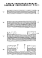
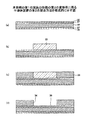
このうち、半導体チップの端子電極の間隔が、配線基板の端子電極の間隔と比べて小さい場合には、直接配線基板に実装することは困難である。図1に、半導体チップ120の端子電極140の間隔D1が、配線基板170の端子電極150の間隔D2と比べて小さい場合の半導体チップ120及び配線基板170の模式的な断面図を示す。このような場合、半導体チップと配線基板との間に、絶縁層と配線層を複雑に積層した高密度多層配線基板を介し、半導体チップをフリップチップにより高密度多層配線基板に実装し、半導体チップを実装した高密度多層配線基板をBGA接合により一般配線基板(マザーボード)に実装する実装方法が行われる。これがFCBGA(Flip Chip Ball Grid Array)である。FCBGAにおいては、高密度多層配線基板を一般配線基板に実装する実装方法がBGAであるが、BGAではなくPGA(Pin Grid Array)、LGA(Land Grid Array)の場合もあり、それぞれFCPGA、FCLGA、と呼ばれる。
Among these, when the distance between the terminal electrodes of the semiconductor chip is smaller than the distance between the terminal electrodes of the wiring board, it is difficult to mount it directly on the wiring board. FIG. 1 is a schematic cross-sectional view of the
しかしながら、上記のようなFCBGA等の場合、絶縁層と配線層を複雑に積層した高密度多層配線基板を用いなくてはならないという問題があった。 However, in the case of the FCBGA as described above, there is a problem that a high-density multilayer wiring board in which an insulating layer and a wiring layer are laminated in a complicated manner must be used.
このような複雑な積層構造を有する高密度多層配線基板を用いずに、半導体チップを直接配線基板と電気的に接続することができる半導体装置の製造方法としては、半導体チップを直接配線基板に埋め込み、内部に実装する方法と、半導体チップを機械的に支持し、発熱した熱を熱伝導する機能を有する基板に実装した半導体装置を、はんだボール等により配線基板に実装する方法と、がある。 As a method for manufacturing a semiconductor device in which a semiconductor chip can be directly electrically connected to a wiring board without using a high-density multilayer wiring board having such a complicated laminated structure, the semiconductor chip is directly embedded in the wiring board. There are a method of mounting inside, and a method of mounting a semiconductor device on a substrate having a function of supporting a semiconductor chip mechanically and conducting heat generated by heat on a wiring board by solder balls or the like.
半導体チップを直接配線基板に埋め込む方法であるが、配線基板の内部に半導体チップを内蔵するための凹部を形成する方法である。特許文献1には、多層配線基板の内部に半導体チップが内蔵され、半導体チップの端子電極がトランジション層を介して配線基板内に配線される方法が開示されている。 A method of embedding a semiconductor chip directly in a wiring board is a method of forming a recess for incorporating the semiconductor chip inside the wiring board. Patent Document 1 discloses a method in which a semiconductor chip is built in a multilayer wiring board, and terminal electrodes of the semiconductor chip are wired in the wiring board through a transition layer.
また、半導体チップを機械的に支持し、発熱した熱を熱伝導する機能を有する基板に実装した半導体装置を、はんだボール等により配線基板に実装する方法であるが、所定の基板に所定の実装方法を用いて実装し、従来の配線基板の端子電極に対応した外部端子電極を形成し、はんだボール等の実装方法を用いて半導体チップを配線基板に実装する方法である。特許文献2には、金属からなる底板と樹脂複合材からなる枠材とで凹部を形成し、前記凹部に半導体チップを埋め込み、絶縁層を設け、従来の配線基板の端子電極に対応した外部端子電極を形成する半導体装置の製造方法の例が開示されている。また、特許文献3には、機械的に安定で高熱伝導率を有する基板を選択し、前記基板に空洞を儲け、半導体チップを取り付け、半導体チップの端子電極と接続される配線と絶縁層からなる薄膜オーバレイを設け、半導体チップと配線基板を接続する半導体装置の製造方法の例が開示されている。
ところが、従来用いられてきた半導体装置の製造方法、半導体装置及び配線基板には、以下のような問題があった。 However, the conventional semiconductor device manufacturing method, semiconductor device, and wiring substrate have the following problems.
まず、特許文献1に開示されている方法であるが、任意の配線基板を用いることができなくなるという問題があった。具体的には、半導体チップを内蔵するための凹部を、配線基板表面にザグリ加工等により形成しなければならず、構造上凹部加工がし易い材質及び構造の配線基板を用意しなくてはならないため、任意の配線基板を用いることができないという問題があった。 First, although it is the method disclosed by patent document 1, there existed a problem that it became impossible to use arbitrary wiring boards. Specifically, a recess for incorporating a semiconductor chip must be formed on the surface of the wiring board by counterboring or the like, and a wiring board made of a material and a structure that is easy to process the recess must be prepared. Therefore, there is a problem that an arbitrary wiring board cannot be used.
また、特許文献2に開示されている方法であるが、枠材を設ける工程が必要になるという問題があった。具体的には、樹脂複合材よりなるパッケージング材に半導体チップの形状に対応した孔を開け、該孔を開けたパッケージング材よりなる枠材を金属板よりなる底板にプレス積層する、という工程が必要になる。加えて、その後上面に絶縁膜を設けるため、枠材の厚さを半導体チップの厚さと等しくしなくてはならない。これらの加工工程の安定性、信頼性に課題があり、その結果、半導体チップを支持する機械的強度や半導体チップからの発熱を放散させるための熱伝導性が低下するという問題があった。
Moreover, although it is the method currently disclosed by
更に、特許文献3に開示されている方法であるが、空洞の形成方法が考慮されていないという問題があった。具体的には、空洞は半導体チップより僅かに大きい寸法にフライス加工される方法が開示されているだけであり、加工精度、信頼性に欠け、C4バンプピッチ等の一般的な端子間隔を有する従来の配線基板に応じて自由に接続端子を設計することは困難である。
Furthermore, although it is the method currently disclosed by
本発明は上記の点に鑑みてなされたものであり、複雑な構造の高密度配線基板を用いずに、半導体チップの端子電極の間隔をC4バンプピッチ等の一般的な端子間隔に対応させることができ、その結果、従来の配線基板を用いながら、半導体チップを支持する機械的強度や半導体チップからの発熱を放散させるための熱伝導性を向上させることができる半導体装置の製造方法及び半導体装置を提供することを目的とする。 The present invention has been made in view of the above points, and the interval between the terminal electrodes of the semiconductor chip is made to correspond to a general terminal interval such as a C4 bump pitch without using a high-density wiring board having a complicated structure. As a result, a semiconductor device manufacturing method and a semiconductor device capable of improving mechanical strength for supporting a semiconductor chip and heat conductivity for dissipating heat generated from the semiconductor chip while using a conventional wiring board The purpose is to provide.
上記の課題を解決するために本発明では、次に述べる各手段を講じたことを特徴とするものである。 In order to solve the above-described problems, the present invention is characterized by the following measures.
第1の発明に係る半導体装置の製造方法は、支持基板の両面にそれぞれ金属層を形成する工程と、前記支持基板の一方の面の前記金属層上に、金属膜を形成する工程と、前記金属膜をエッチングし、嵌合孔を形成する工程と、前記嵌合孔内に、複数の端子電極が設けられた面が上方を向くよう、半導体チップを実装する工程と、前記支持基板上に、前記半導体チップの前記端子電極が設けられた面と側面とを覆う絶縁層を形成する工程と、前記絶縁層上に、前記端子電極と接続する金属配線を形成する工程と、前記金属配線上に複数の外部端子電極を形成する工程と、を有し、それぞれの前記金属層は、前記金属膜のエッチングにより除去されないエッチングストッパ層を含み、隣接する前記外部端子電極の間隔が、隣接する前記端子電極の間隔より大きいことを特徴とする。 According to a first aspect of the present invention, there is provided a method for manufacturing a semiconductor device, comprising: forming a metal layer on each side of a support substrate ; forming a metal film on the metal layer on one side of the support substrate ; Etching a metal film to form a fitting hole; mounting a semiconductor chip in the fitting hole so that a surface provided with a plurality of terminal electrodes faces upward; and on the support substrate A step of forming an insulating layer covering a surface and a side surface of the semiconductor chip on which the terminal electrode is provided, a step of forming a metal wiring connected to the terminal electrode on the insulating layer, and the metal wiring Forming a plurality of external terminal electrodes, and each of the metal layers includes an etching stopper layer that is not removed by etching of the metal film, and the interval between the adjacent external terminal electrodes is adjacent to each other. Terminal electrode It is greater than septum.
第2の発明に係る半導体装置は、両面にそれぞれ金属層が形成された支持基板と、前記支持基板の一方の面の前記金属層上に形成された嵌合孔を有する金属膜と、前記嵌合孔内に、複数の端子電極が設けられた面が上方を向くよう実装された半導体チップと、前記支持基板上に、前記半導体チップの前記端子電極が設けられた面と側面とを覆うよう形成された絶縁層と、前記絶縁層上に、前記端子電極と接続して形成された金属配線と、前記金属配線上に複数形成された外部端子電極と、を有し、前記支持基板の一方の面の前記金属層及び前記支持基板の他方の面の前記金属層は、それぞれ、前記金属膜を形成する金属材料とは異なる金属材料を含み、隣接する前記外部端子電極の間隔が、隣接する前記端子電極の間隔より大きいことを特徴とする。
According to a second aspect of the present invention, there is provided a semiconductor device including a support substrate having a metal layer formed on both surfaces thereof, a metal film having a fitting hole formed on the metal layer on one surface of the support substrate, and the fitting. A semiconductor chip mounted so that a surface provided with a plurality of terminal electrodes faces upward in the joint hole, and a surface and side surfaces of the semiconductor chip provided with the terminal electrodes are covered on the support substrate. One of the support substrates , comprising: an insulating layer formed; a metal wiring connected to the terminal electrode on the insulating layer; and a plurality of external terminal electrodes formed on the metal wiring. The metal layer on the other surface and the metal layer on the other surface of the support substrate each include a metal material different from the metal material forming the metal film, and the interval between adjacent external terminal electrodes is adjacent It is larger than the interval between the terminal electrodes To.
本発明によれば、半導体チップの端子電極の間隔をC4バンプピッチ等の一般的な端子間隔に対応させることによって従来の配線基板を用いることができ、半導体チップを支持する機械的強度や半導体チップからの発熱を放散させるための熱伝導性を向上させることができる。 According to the present invention, a conventional wiring board can be used by making the interval between terminal electrodes of a semiconductor chip correspond to a general terminal interval such as a C4 bump pitch, and the mechanical strength or semiconductor chip supporting the semiconductor chip can be used. The heat conductivity for dissipating the heat generated from can be improved.
次に、本発明を実施するための最良の形態について図面と共に説明する。
(第1の実施の形態)
図2乃至図3Bを参照し、本発明の第1の実施の形態に係る半導体装置を説明する。
Next, the best mode for carrying out the present invention will be described with reference to the drawings.
(First embodiment)
A semiconductor device according to the first embodiment of the present invention will be described with reference to FIGS. 2 to 3B.
最初に、図2を参照し、本実施の形態に係る半導体装置を説明する。 First, the semiconductor device according to the present embodiment will be described with reference to FIG.
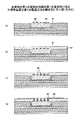
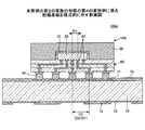
図2は、本実施の形態に係る半導体装置を模式的に示す断面図である。 FIG. 2 is a cross-sectional view schematically showing the semiconductor device according to the present embodiment.
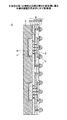
図2に示されるように、本実施の形態に係る半導体装置10は、半導体チップ20と、支持基板30と、端子電極40と、外部端子電極50と、ファンアウト部60と、を有する。
As shown in FIG. 2, the
半導体チップ20は、半導体装置10の電気的な機能を有する。半導体チップ20は、半導体チップ20の外部と電気的に接続するための端子電極40を有する。隣接する端子電極40同士の間隔を第1の間隔D1とする。例えば、D1は50〜100μm程度とすることができる。
The
支持基板30には、接着剤31を介して半導体チップ20が、端子電極40が設けられた面と反対側の面をもって接着される。支持基板30は、半導体チップ20を支持し、半導体装置10の機械的な強度を確保すると同時に、半導体チップ20で発熱される熱を放熱するためのものである。
The
外部端子電極50は、ファンアウト部60の最表面に設けられる。外部端子電極50は、半導体装置10の外部と電気的に接続するための端子電極である。隣接する外部端子電極50同士の間隔を第2の間隔D2とする。例えば、D2は150μm〜180μm程度とすることができる。
The external
ここで、外部端子電極50の全てにおいて、隣接する外部端子電極50同士の間隔D2は、端子電極40の全てにおいて、隣接する端子電極40同士の間隔D1よりも大きい。即ち、隣接する外部端子電極50同士の最小間隔は、隣接する端子電極40同士の最大間隔よりも大きい。
Here, in all the external
ファンアウト部60は、絶縁層61と、貫通電極62と、金属配線63と、を有する。ファンアウト部60は、第1の間隔D1を有する端子電極40と、第2の間隔D2を有する外部端子電極50と、を接続するためのものである。
The fan-out
絶縁層61は、半導体チップ20及び半導体チップ20に設けられた端子電極40を被覆するように、設けられる。貫通電極62は、端子電極40と接続され、絶縁層61を貫通するように設けられる。金属配線63は、貫通電極62と接続され、絶縁層61の表面を配線される。
The insulating
絶縁層61は、支持基板30に接着剤31を介して接着された半導体チップ20の端子電極40が設けられた面を被覆する。また、図2に示されるように、半導体チップ20の側面を被覆することができる。
The insulating
絶縁層61、貫通電極62、金属配線63は、少なくとも1層ずつ形成される。D1とD2がほぼ等しいときは、絶縁層61、貫通電極62、金属配線63は、それぞれ1層ずつ形成し、端子電極40と、外部端子電極50と、を電気的に接続することができる。しかし、例えばD2がD1の2倍程度あるなど、D2がD1よりかなり大きい場合は、配線が交錯することを避けるため、絶縁層61、貫通電極62、金属配線63は、それぞれ複数層ずつ形成することができる。本実施の形態では、図2に示されるように、絶縁層61、貫通電極62、金属配線63がそれぞれ3層ずつ形成されており、支持基板30及び半導体チップ20に近い方から順に、絶縁層61、61a、61b、貫通電極62、62a、62b、金属配線63、63a、63bとする。前述した外部端子電極50は、ファンアウト部60の最表面に設けられた金属配線63bに接続されるように設けられる。
The insulating
次に、本実施の形態に係る半導体装置10による、半導体チップ20の隣接する端子電極40同士の間隔である第1の間隔D1を隣接する外部端子電極50同士の間隔である第2の間隔D2に広げるファンアウト機能、機械的強度確保の機能、及び熱伝導性確保の機能について説明する。
Next, in the
まず、ファンアウト機能について説明する。 First, the fan-out function will be described.
始めに、貫通電極62は、端子電極40に接続して垂直に形成されるため、その間隔は、第1の間隔D1と同一である。
First, since the through
次に、5つの貫通電極62に接続された5つの金属配線63のうち、左右外側を除いた中心の3つの金属配線63は、貫通電極62の直上に接続して形成されるため、その間隔は第1の間隔D1と同一である。しかし、左右外側の2つの貫通電極62に接続された金属配線63は、左右外側の2つの貫通電極62の位置から左右外側に向かって配線される。これは、第1の間隔D1を第2の間隔D2に広げるためである。本実施の形態では、例えば、左右両側の2つの金属配線63は、中心の貫通電極から2×D2の距離まで配線される。
Next, among the five
次に、貫通電極62aは、金属配線63に接続して垂直に形成されるため、左右外側を除いた中心の3つの貫通電極62aの間隔は、第1の間隔D1と同一であり、左右外側の2つの貫通電極62aは、中心の貫通電極62aと2×D2の間隔を有する。
Next, since the through
次に、5つの貫通電極62aに接続された5つの金属配線63aのうち、中心と、左右一番外側に位置する3つの金属配線63aは、貫通電極62aの直上に接続して形成される。しかし、左右外側から2番目に位置する2つの金属配線63aは、貫通電極62aの位置から左右外側に向かって配線される。これは、第1の間隔D1を第2の間隔D2に広げるためである。本実施の形態では、例えば、左右外側から2番目に位置する2つの金属配線63aは、中心の貫通電極からD2の距離まで配線される。
Next, among the five
次に、貫通電極62bは、金属配線63aに接続して垂直に形成される。そのため、5つの貫通電極62bの間隔は、第2の間隔D2と同一である。
Next, the through
次に、5つの金属配線63bは、5つの貫通電極62bの直上に接続して形成される。そのため、5つの金属配線63bの間隔は、第2の間隔D2と同一である。
Next, the five
最後に、5つの金属配線63bに接続して5つの外部端子電極50が形成される。従って、端子電極40の間隔である第1の間隔D1は、第2の間隔D2に広げられた外部の端子電極50に接続される。
Finally, five external
以上のようにして、隣接する端子電極40同士の間隔である第1の間隔D1を隣接する外部端子電極50同士の間隔である第2の間隔D2に広げるファンアウト機能が機能する。
As described above, the fan-out function that expands the first interval D1 that is the interval between the adjacent
次に、半導体装置10の機械的強度確保の機能及び熱伝導性確保の機能について説明する。
Next, the function of ensuring the mechanical strength and the function of ensuring thermal conductivity of the
半導体装置10は、半導体チップ20と端子電極40と同数の外部端子電極50を有し、隣接する外部端子電極50同士の間隔である第2の間隔D2は、隣接する端子電極40同士の間隔である第1の間隔D1に比べて大きい。従って、半導体装置10の面積は半導体チップ20の面積に比べて大きい。半導体チップ20に比べて大きな半導体装置10の機械的強度は、主として支持基板30によって確保される。また、本実施の形態に係る半導体装置10では、接着剤31、絶縁層61は、半導体チップ20を支持基板30に固定するために用いられるため、接着剤31、絶縁層61によっても機械的強度は確保される。
The
一方、半導体チップ20は、接着剤31、絶縁層61を通じて支持基板30に熱的に接触される。また、端子電極40から貫通電極62、62a、62b、金属配線63、63a、63bを通じて外部端子電極50に電気的に接続されると同時に、熱的にも接続される。従って、本実施の形態に係る半導体装置10では、半導体チップ20で発生される熱を放熱するための熱伝導性は確保される。
On the other hand, the
次に、半導体装置10を構成する好適な材料を説明する。
Next, a suitable material constituting the
まず、支持基板30であるが、特に限定されないものの、例えば、銅板、アルミ板またはコバール板等の金属板を用いることができる。絶縁層61であるが、特に限定されないものの、例えば、エポキシ系樹脂、フェノール系樹脂、フェノキシ樹脂、ポリイミド系樹脂、ポリフェニレン系樹脂、ポリオレフィン系樹脂、フッ素系樹脂を用いることができる。貫通電極62であるが、特に限定されないものの、例えば、銅を用いることができる。接着剤31であるが、特に限定されないものの、例えば、エポキシ樹脂に銀を添加させた高熱伝導性エポキシ接着剤又は金シリコンを用いることができる。金属配線63であるが、特に限定されないものの、例えば、スズ、クロム、チタン、ニッケル、亜鉛、コバルト、金、銅などを用いることができる。外部端子電極50であるが、特に限定されないものの、例えば、半田を用いることができる。
(第1の実施の形態に係る半導体装置の製造方法)
次に、図3A及び図3Bを参照し、本実施の形態に係る半導体装置の製造方法について説明する。
First, although it is the
(Method for Manufacturing Semiconductor Device According to First Embodiment)
Next, with reference to FIGS. 3A and 3B, a method for manufacturing the semiconductor device according to the present embodiment will be described.
図3A及び図3Bは、本実施の形態に係る半導体装置の製造方法を模式的に示す図である。 3A and 3B are diagrams schematically showing a method for manufacturing a semiconductor device according to the present embodiment.
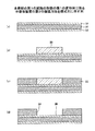
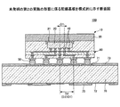
まず、図3A(a)に示される半導体チップ実装工程において、支持基板30上に、半導体チップ20を接着する。この場合、例えば厚さが100〜1000μmの銅板よりなる支持基板30上の半導体チップ20が接着される接着面に、予め接着剤31を塗布し、該接着剤31が塗布された支持基板30上に、半導体チップ20を載置し、接着する。また、半導体チップ20は、端子電極40が設けられた面が露出(フェイスアップ)されるように支持基板30に接着される。
First, in the semiconductor chip mounting process shown in FIG. 3A (a), the
次に、図3A(b)に示される絶縁層形成工程において、エポキシ系樹脂又はポリイミド系樹脂よりなる絶縁層61を形成する。このとき、例えば100〜800μmの高さの半導体チップ20の端子電極40が設けられた面を、更に、例えば5〜30μmの厚さで覆うように、絶縁層61を形成する。すなわち、絶縁層61の厚さは、半導体チップ20の高さである例えば100〜800μmと、半導体チップ20の端子電極40を被覆する厚さである例えば5〜30μmと、の合計であり、半導体チップ20の端子電極40は、絶縁層61によって被覆される。また、半導体チップ20の側面21を隙間なく覆うように、絶縁層61を形成することもできる。本実施の形態では、図3A(b)に示されるように、半導体チップ20の側面21も絶縁層61によって隙間なく覆われる。
Next, in the insulating layer forming step shown in FIG. 3A (b), an insulating
次に、図3A(c)に示される工程において、加工方法は特に限定されるものではないが、例えばレーザにより、絶縁層61に、端子電極40にまで到達する貫通孔64を形成する。
Next, in the step shown in FIG. 3A (c), the processing method is not particularly limited. For example, the through
次に、図3A(d)に示される貫通電極形成工程及び金属配線形成工程において、例えば、セミアディティブ法により、前記貫通孔64を埋設するように貫通電極62を形成するとともに、貫通電極62と接続される金属配線63を形成する。
Next, in the through electrode forming step and the metal wiring forming step shown in FIG. 3A (d), the through
このとき、図3A(d)に図示される5つの端子電極40のうち、左右両側の一番外側にある2つの端子電極40に接続された金属配線63は、端子間隔を広げるため、左右両側に広がるように配設される。
At this time, among the five
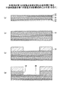
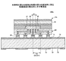
次に、図3B(a)及び図3B(b)に示される工程において、図3A(b)〜図3A(d)に示された絶縁層61の形成、絶縁層61への貫通孔64の形成、貫通電極62及び金属配線63の形成を2回繰返す。ただし、1回目の繰返しにおいて、絶縁層は61a、貫通孔は64a、貫通電極は62a、金属配線は63a、であり、2回目の繰返しにおいて、絶縁層は61b、貫通孔は64b、貫通電極は62b、金属配線は63b、である。絶縁層61a、61bの厚さは、例えば5〜30μmとすることができる。金属配線63aにおいて、図3B(a)に図示される5つの端子電極40のうち、左右両側とも外側から2番目に位置する2つの端子電極に接続された金属配線63aは、端子間隔を広げるため、左右両側に広がるように配設される。その結果、2回目の繰返しにおいて、図3B(b)に示されるように、貫通電極62b、金属配線63bは、第1の間隔D1より広い第2の間隔D2をもって等間隔に配設される。
Next, in the steps shown in FIGS. 3B (a) and 3B (b), the formation of the insulating
次に、図3B(c)に示される外部端子電極形成工程において、金属配線63bに接続された外部端子電極50を形成する。外部端子電極50は、半田又は電解めっきによる銅を形成することにより、形成される。
Next, in the external terminal electrode formation step shown in FIG. 3B (c), the external
以上、本実施の形態に係る半導体装置によれば、半導体チップの端子電極の間隔をC4バンプピッチ等の一般的な端子間隔に対応させることによって従来の配線基板を用いることができ、半導体チップを支持する機械的強度や半導体チップからの発熱を放散させるための熱伝導性を向上させることができる。 As described above, according to the semiconductor device of the present embodiment, the conventional wiring substrate can be used by making the interval between the terminal electrodes of the semiconductor chip correspond to the general terminal interval such as the C4 bump pitch. The mechanical strength to support and the thermal conductivity for dissipating the heat generated from the semiconductor chip can be improved.
なお、本実施の形態に係る半導体装置10では、ファンアウト機能を確保するために3層の絶縁層61、貫通電極62、金属配線63を用いているが、任意の端子電極40が互いに交錯することなく外部端子電極50に接続されることが可能であれば、層数、金属配線の長さは、これに限られるものではない。
In the
また、本実施の形態に係る半導体装置の製造方法では、例えばセミアディティブ法により、貫通電極62、62a、62bを形成するとともに、金属配線63、63a、63bを形成するが、貫通電極62、62a、62bと、金属配線63、63a、63bと、を別々の工程により形成してもよい。
(第1の実施の形態の第1の変形例)
次に、図4乃至図6を参照し、本発明の第1の実施の形態の第1の変形例について説明する。
In the method for manufacturing the semiconductor device according to the present embodiment, the through
(First modification of the first embodiment)
Next, a first modification of the first embodiment of the present invention will be described with reference to FIGS.
最初に、図4を参照し、本変形例に係る半導体装置を説明する。 First, a semiconductor device according to this modification will be described with reference to FIG.
図4は、本変形例に係る半導体装置を模式的に示す断面図である。ただし、以下の文中では、先に説明した部分には同一の符号を付し、説明を省略する場合がある(以下の変形例についても同様)。 FIG. 4 is a cross-sectional view schematically showing a semiconductor device according to this modification. However, in the following text, the parts described above are denoted by the same reference numerals, and description thereof may be omitted (the same applies to the following modified examples).
本変形例に係る半導体装置は、支持基板上に第1の金属膜を介して第2の金属膜が設けられ、該第2の金属膜に、半導体チップを嵌合する嵌合孔が形成される点で、第1の実施の形態に係る半導体チップと相違する。 In the semiconductor device according to this modification, a second metal film is provided on a support substrate via a first metal film, and a fitting hole for fitting a semiconductor chip is formed in the second metal film. This is different from the semiconductor chip according to the first embodiment.
図4を参照するに、第1の実施の形態において、半導体チップが接着剤により支持基板に接着され、端子電極が設けられた面が絶縁層で被覆されるのと相違し、本変形例に係る半導体装置10aは、支持基板30上に第1の金属膜32を介して第2の金属膜33が設けられ、該第2の金属膜33に、半導体チップ20を嵌合する嵌合孔34が形成され、半導体チップ20は端子電極40が設けられた面が露出されるように嵌合孔34に嵌合され、接着剤31により嵌合孔34に接着されることが特徴である。
Referring to FIG. 4, in the first embodiment, the semiconductor chip is bonded to the support substrate with an adhesive and the surface on which the terminal electrode is provided is covered with an insulating layer. In the
図4に示されるように、本変形例に係る半導体装置10aは、半導体チップ20と、支持基板30と、端子電極40と、外部端子電極50と、ファンアウト部60と、を有する。半導体チップ20、端子電極40、外部端子電極50の構造は、第1の実施の形態に係る半導体装置10と同一である。
As illustrated in FIG. 4, the
一方、支持基板30は、両面を第1の金属膜32で被覆される。また支持基板30の片面には、第1の金属膜32を介して第2の金属膜33が形成される。第2の金属膜33の厚さは、半導体チップ20の高さとほぼ同一である。第2の金属膜は、平面視において半導体チップ20とほぼ同一の形状に除去され、嵌合孔34が形成される。嵌合孔34には、接着剤31を介して半導体チップ20が、端子電極40が設けられた面と反対側の面をもって接着される。
On the other hand, both sides of the
また、ファンアウト部60を構成する最初の絶縁層61は、第1の実施の形態において、半導体チップ20の高さとほぼ同一の厚さを有する部分があるのに対し、本変形例では、半導体チップ20と嵌合孔34との隙間を除いた全ての部分で、半導体チップ20の端子電極40を被覆する厚さを有する。
In addition, in the first embodiment, the first insulating
次に、ファンアウト機能、機械的強度確保の機能、熱伝導性確保の機能であるが、ファンアウトの機能については、第1の実施の形態と同様の機能を有する。また、機械的強度、熱伝導性については、半導体チップ20が嵌合孔34に嵌合されることにより、半導体チップ20の側面が第2の金属膜33で覆われる。そのため、第1の実施の形態と比較して、より機械的強度、熱伝導性を向上させることができる。
Next, a fan-out function, a mechanical strength ensuring function, and a thermal conductivity securing function are provided. The fan-out function has the same functions as those in the first embodiment. As for mechanical strength and thermal conductivity, the side surface of the
次に、半導体装置10aを構成する好適な材料を説明する。絶縁層61、貫通電極62、接着剤31、金属配線63、外部端子電極50は、第1の実施の形態と同一の材料を用いることができる。
Next, a suitable material constituting the
支持基板30であるが、特に限定されないものの、例えば、ニッケル板を用いることができる。また、第1の金属膜であるが、特に限定されないものの、例えば、金を用いることができる。さらに、第2の金属膜として、特に限定されないものの、例えば、銅を用いることができる。
(第1の実施の形態の第1の変形例に係る半導体装置の第1の製造方法)
次に、図5A乃至図5Cを参照し、本変形例に係る半導体装置の第1の製造方法について説明する。
Although it is the
(First Manufacturing Method of Semiconductor Device According to First Modification of First Embodiment)
Next, a first method for manufacturing a semiconductor device according to this modification will be described with reference to FIGS. 5A to 5C.
図5A乃至図5Cは、本変形例に係る半導体装置の第1の製造方法を模式的に示す図である。 5A to 5C are diagrams schematically showing a first manufacturing method of a semiconductor device according to this modification.
まず、図5A(a)に示されるように、例えば厚さが100〜1000μmのニッケル板よりなる支持基板30を用意する。予め、ニッケル板よりなる支持基板30の両面には、金の電解めっきを行い、例えば厚さが30〜400nmの金よりなる第1の金属膜32を形成しておく。
First, as shown in FIG. 5A (a), a
次に、図5A(b)に示される金属膜形成工程において、支持基板30に金めっきによって形成された第1の金属膜32上に、銅の電解めっきを行い、例えば厚さが100〜800μmの銅よりなる第2の金属膜33を形成する。この100〜800μmの厚さは、例えば100〜800μmの半導体チップ20の高さにほぼ等しい。
Next, in the metal film forming step shown in FIG. 5A (b), copper is electroplated on the
次に、図5A(c)に示される嵌合孔形成工程において、第2の金属膜33上にドライフィルムレジスト35よりなるレジストパターンを形成する。即ち、第2の金属膜33上に、例えば厚さが10〜30μmのドライフィルムレジスト35を積層し、ドライフィルムレジスト35を露光、現像し、半導体チップ20の平面視における形状に対応した部分を除去したレジストパターンを形成する。このレジストパターンの形状は、その後第2の金属膜33に形成される半導体チップ20を嵌合するための嵌合孔34の形状に対応したものである。
Next, in the fitting hole forming step shown in FIG. 5A (c), a resist pattern made of the dry film resist 35 is formed on the
次に、図5A(d)に示される嵌合孔形成工程において、第2の金属膜33上に形成されたドライフィルムレジスト35よりなるレジストパターンをエッチング保護膜とし、塩化第二銅をエッチング液として、銅よりなる第2の金属膜33をエッチングし、嵌合孔34を形成する。このとき、銅よりなる第2の金属膜33の深さ方向にエッチングが進展していくが、金めっきにより形成された第1の金属膜32の表面にエッチングが達すると、エッチングの進展が止まるため、半導体チップ20を嵌合する嵌合孔34の半導体チップ20を搭載する搭載面36の平坦性を確保することができる。また、嵌合孔34の深さは第2の金属膜33の厚さに等しく、第2の金属膜33の厚さは、例えば100〜800μmである半導体チップ20の高さにほぼ等しいため、嵌合孔34の深さは半導体チップ20の高さにほぼ等しい。
Next, in the fitting hole forming step shown in FIG. 5A (d), a resist pattern made of the dry film resist 35 formed on the
次に、図5B(a)に示される嵌合接着工程において、嵌合孔34に半導体チップ20を嵌合し、接着剤31を用いて半導体チップ20を嵌合孔34に接着する。ここで、接着剤31であるが、高熱伝導性エポキシ接着剤を用いることもできるが、搭載面36が金で形成されているため、半導体チップ20との間での金シリコンによる共晶結合により接着することもできる。
Next, in the fitting and bonding step shown in FIG. 5B (a), the
次に、図5B(b)に示される絶縁層形成工程において、エポキシ系樹脂又はポリイミド系樹脂よりなる絶縁層61を形成する。具体的には、嵌合孔34に嵌合された半導体チップ20の端子電極40が設けられた面及び第2の金属膜33の表面を覆うように、例えば厚さが5〜30μmの絶縁層61を形成する。前述したように、嵌合孔34の深さは半導体チップ20の高さにほぼ等しいため、嵌合孔34に嵌合された半導体チップ20の端子電極40が設けられた面及び第2の金属膜33の表面はほぼ等しい高さである。加えて、半導体チップ20の側面21と嵌合孔34との隙間も絶縁層61で埋められる。以上のようにして、半導体チップ20の端子電極40は、絶縁層61によって被覆され、平坦化される。
Next, in an insulating layer forming step shown in FIG. 5B (b), an insulating
次に、例えばレーザにより、貫通孔64を形成し(図5B(c))、例えば、セミアディティブ法により、貫通電極62を形成するとともに金属配線63を形成する(図5B(d))。更に、図5B(b)〜図5B(d)の工程を2回繰り返してファンアウト部60を形成し(図5C(a)及び図5C(b))、外部端子電極50を形成する(図5C(c))。これらの図5B(c)、図5B(d)、図5C(a)〜図5C(c)に示される工程は、第1の実施の形態の製造方法において図3A(c)、図3A(d)、図3B(a)〜図3B(c)に示される工程と同一である。また、1回目の繰返しにおいて、絶縁層は61a、貫通孔は64a、貫通電極は62a、金属配線は63a、であり、2回目の繰返しにおいて、絶縁層は61b、貫通孔は64b、貫通電極は62b、金属配線は63b、であるのは、第1の実施の形態と同一である。
(第1の実施の形態の第1の変形例に係る半導体装置の第2の製造方法)
次に、図5B乃至図6を参照し、本変形例に係る半導体装置の第2の製造方法について説明する。
Next, the through
(Second Method for Manufacturing Semiconductor Device According to First Modification of First Embodiment)
Next, a second method for manufacturing a semiconductor device according to this variation will be described with reference to FIGS. 5B to 6.
本製造方法は、アディティブ工法を用いて第2の金属膜に嵌合孔を形成する点で、本変形例に係る半導体装置の第1の製造方法と相違する。 This manufacturing method is different from the first manufacturing method of the semiconductor device according to this modification in that a fitting hole is formed in the second metal film using an additive method.
図6を参照するに、本変形例に係る半導体装置の第1の製造方法において、支持基板上に第2の金属膜を形成した後、嵌合孔に対応したレジストパターンを形成し、第2の金属膜をエッチングして嵌合孔を形成するのと相違し、本製造方法は、支持基板上に第1の金属膜を形成した後、第2の金属膜を形成する前に、嵌合孔に対応したレジストパターンを形成し、その後、第2の金属膜を形成し、レジストパターンを除去し、第2の金属膜に嵌合孔を形成することが特徴である。 Referring to FIG. 6, in the first manufacturing method of the semiconductor device according to this modification, after forming the second metal film on the support substrate, a resist pattern corresponding to the fitting hole is formed, and the second Unlike the case where the fitting hole is formed by etching the metal film, the manufacturing method is performed after the first metal film is formed on the support substrate and before the second metal film is formed. A feature is that a resist pattern corresponding to the hole is formed, then a second metal film is formed, the resist pattern is removed, and a fitting hole is formed in the second metal film.
図6は、本変形例に係る半導体装置の第2の製造方法を模式的に示す図である。また以下では、図6(a)〜図6(d)、図5B(a)〜図5B(d)、図5C(a)〜図5C(c)を用いて、本製造方法を説明する。 FIG. 6 is a diagram schematically showing a second manufacturing method of the semiconductor device according to this modification. Moreover, below, this manufacturing method is demonstrated using FIG. 6 (a)-FIG.6 (d), FIG.5B (a)-FIG.5B (d), FIG.5C (a)-FIG.5C (c).
まず、図6(a)に示されるように、例えば厚さが100〜1000μmのニッケル板よりなる支持基板30を用意する。予め、ニッケル板よりなる支持基板30の両面には、金の電解めっきを行い、例えば厚さが30〜400nmの金よりなる第1の金属膜32を形成しておく。これは、本変形例に係る半導体装置の第1の製造方法において図5A(a)に示される工程と同一である。
First, as shown in FIG. 6A, a
次に、図6(b)に示される工程において、第1の金属膜32上にドライフィルムレジスト35よりなるレジストパターンを形成する。即ち、第1の金属膜32上に、例えば厚さが10〜30μmのドライフィルムレジスト35を積層し、ドライフィルムレジスト35を露光、現像し、半導体チップ20の平面視における形状に対応した形状を有するレジストパターンを形成する。このレジストパターンの形状は、その後第2の金属膜33に形成される半導体チップ20を嵌合するための嵌合孔34の形状に対応したものである。ただし、本変形例に係る半導体装置の第1の製造方法と比べると、レジストパターンの形状はポジネガ逆のパターンの形状になっている。
Next, in the step shown in FIG. 6B, a resist pattern made of the dry film resist 35 is formed on the
次に、図6(c)に示される工程において、レジストパターンの形成された第1の金属膜32上に、銅の電解めっきを行い、例えば厚さ100〜800μmの銅よりなる第2の金属膜33を形成する。この100〜800μmの厚さは、例えば100〜800μmの半導体チップ20の高さにほぼ等しい。
Next, in the step shown in FIG. 6C, copper is electroplated on the
次に、図6(d)に示される工程において、レジストパターンとして残っているドライフィルムレジスト35の全面を露光、現像し、ドライフィルムレジストを剥離する。その結果、第2の金属膜33に、半導体チップ20を嵌合するための嵌合孔34が形成される。嵌合孔34の深さは第2の金属膜33の厚さに等しく、第2の金属膜33の厚さは、例えば100〜800μmである半導体チップ20の高さにほぼ等しいため、嵌合孔34の深さは半導体チップ20の高さにほぼ等しい。
Next, in the step shown in FIG. 6D, the entire surface of the dry film resist 35 remaining as a resist pattern is exposed and developed, and the dry film resist is peeled off. As a result, a
それ以後、嵌合孔34に半導体チップ20を嵌合して接着する工程から、外部端子電極50を形成する工程は、本変形例に係る半導体装置の第1の製造方法における図5B(a)〜図5B(d)、図5C(a)〜図5C(c)と同一の工程を行う。
Thereafter, from the step of fitting and bonding the
以上、本変形例に係る半導体装置によれば、半導体チップの端子電極の間隔をC4バンプピッチ等の一般的な端子間隔に対応させることができ、半導体チップが嵌合孔に嵌合されることにより、より機械的強度、熱伝導性を向上させることができる。 As mentioned above, according to the semiconductor device concerning this modification, the interval of the terminal electrode of a semiconductor chip can be made to correspond to general terminal intervals, such as C4 bump pitch, and a semiconductor chip is fitted in a fitting hole. Thus, mechanical strength and thermal conductivity can be further improved.
なお、本変形例に係る半導体装置10aでは、ファンアウト機能を確保するために3層の絶縁層61、貫通電極62、金属配線63を用いているが、任意の端子電極40が互いに交錯することなく外部端子電極50に接続されることが可能であれば、層数、金属配線の長さは、これに限られるものではない。
In the
また、本実施の形態に係る半導体装置の製造方法では、例えば、セミアディティブ法により、貫通電極62、62a、62bを形成するとともに、金属配線63、63a、63bを形成するが、貫通電極62、62a、62bと、金属配線63、63a、63bと、を別々の工程により形成してもよい。
(第1の実施の形態の第2の変形例)
次に、図7乃至図9を参照し、本発明の第1の実施の形態の第2の変形例について説明する。
In the method for manufacturing a semiconductor device according to the present embodiment, the through
(Second modification of the first embodiment)
Next, a second modification of the first embodiment of the present invention will be described with reference to FIGS.
最初に、図7を参照し、本変形例に係る半導体装置を説明する。 First, a semiconductor device according to this modification will be described with reference to FIG.
図7は、本変形例に係る半導体装置を模式的に示す断面図である。 FIG. 7 is a cross-sectional view schematically showing a semiconductor device according to this modification.
本変形例に係る半導体装置は、支持基板上に形成される第1の金属膜が支持基板表面処理膜を介して設けられる点で、第1の実施の形態の第1の変形例に係る半導体装置と相違する。 The semiconductor device according to this modification is the semiconductor according to the first modification of the first embodiment in that the first metal film formed on the support substrate is provided via the support substrate surface treatment film. Different from the device.
図7を参照するに、第1の実施の形態の第1の変形例において、第1の金属膜が支持基板上に直接形成されるのと相違し、本変形例に係る半導体装置10bは、第1の金属膜32が、支持基板表面処理膜37を介して支持基板30上に形成されることが特徴である。
Referring to FIG. 7, unlike the first modification of the first embodiment in which the first metal film is formed directly on the support substrate, the
図7に示されるように、本変形例に係る半導体装置10bは、半導体チップ20と、支持基板30と、端子電極40と、外部端子電極50と、ファンアウト部60と、を有する。半導体チップ20、端子電極40、外部端子電極50、ファンアウト部60の構造は、第1の実施の形態の第1の変形例に係る半導体装置10aと同一である。
As shown in FIG. 7, the
一方、支持基板30は、両面を支持基板表面処理膜37で被覆され、その表面を第1の金属膜32で被覆される。また支持基板30の片面において、第1の金属膜32の表面に第2の金属膜33が形成される。第2の金属膜33の厚さが、半導体チップ20の高さとほぼ等しく、嵌合孔34が形成され、嵌合孔34に半導体チップ20が嵌合され、接着されるのは、第1の実施の形態の第1の変形例と同一である。
On the other hand, the
第1の金属膜32が、支持基板表面処理膜37を介して支持基板30上に形成されるのは、支持基板30及び第1の金属膜32の組合せとして、任意の材料の組合せを用いるためである。即ち、第2の金属膜33のエッチングストッパ層として機能する第1の金属膜32を支持基板30上に直接形成することが難しい場合、支持基板表面処理膜37を介することによって、第1の金属膜32を支持基板30上に形成することができる。
The
具体的には、支持基板30として例えば銅板を用い、第1の金属膜32として例えば金めっきによる金を用いる場合、銅板上に直接金めっきを行うと、金と銅が拡散してしまい、金めっきを行うことができない。従って、金と銅の拡散バリアとして、例えばニッケルよりなる支持基板表面処理膜37を支持基板30の表面に設ける。その他の好適な材料は、第1の実施の形態の第1の変形例と同一のものを用いることができる。
Specifically, for example, when a copper plate is used as the
また、ファンアウト機能、機械的強度確保の機能、熱伝導性確保の機能については、第1の実施の形態の第1の変形例と同様の機能を有するため、特に、機械的強度、熱伝導性については、第1の実施の形態と比較して、より機械的強度、熱伝導性を向上させることができる。
(第1の実施の形態の第2の変形例に係る半導体装置の第1の製造方法)
次に、図8A乃至図8Cを参照し、本変形例に係る半導体装置の第1の製造方法について説明する。
Further, the fanout function, the mechanical strength securing function, and the thermal conductivity securing function have the same functions as those of the first modification of the first embodiment. As for the properties, compared to the first embodiment, the mechanical strength and thermal conductivity can be improved.
(First Method for Manufacturing Semiconductor Device According to Second Modification of First Embodiment)
Next, a first method for manufacturing a semiconductor device according to this variation will be described with reference to FIGS. 8A to 8C.
図8A乃至図8Cは、本変形例に係る半導体装置の第1の製造方法を模式的に示す図である。 8A to 8C are views schematically showing a first method for manufacturing a semiconductor device according to this variation.
まず、図8A(a)に示されるように、例えば厚さが100〜1000μmの銅板よりなる支持基板30を用意する。予め、銅板よりなる支持基板30の両面には、ニッケルの無電解めっきを行い、例えば厚さが3〜10μmのニッケルよりなる支持基板表面処理膜37を形成する。次に、金の電解めっきを行い、例えば厚さが30〜400nmの金よりなる第1の金属膜32を形成する。
First, as shown in FIG. 8A (a), a
次に、銅の電解めっきを行って銅よりなる第2の金属膜33を形成し(図8A(b))、第2の金属膜33上にドライフィルムレジスト35よりなるレジストパターンを形成し(図8A(c))、銅よりなる第2の金属膜33を第1の金属膜32の表面までエッチングして嵌合孔34を形成し(図8A(d))、嵌合孔34に半導体チップ20を嵌合して接着し(図8B(a))、半導体チップ20の端子電極40を被覆するように、絶縁層61を形成する(図8B(b))。更に、例えばレーザにより、貫通孔64を形成し(図8B(c))、例えば、セミアディティブ法により、貫通電極62を形成するとともに金属配線63を形成する(図8B(d))。これらの図8A(b)〜図8A(d)、図8B(a)〜図8B(d)に示される工程は、第1の実施の形態の第1の変形例において図5A(b)〜図5A(d)、図5B(a)〜図5B(d)に示される工程と同一である。
Next, copper is electroplated to form a
次に、図8B(b)〜図8B(d)の工程を2回繰り返してファンアウト部60を形成し(図8C(a)及び図8C(b))、外部端子電極50を形成する(図8C(c))。これらの図8C(a)〜図8C(c)に示される工程は、第1の実施の形態の第1の変形例において図5C(a)〜図5C(c)に示される工程と同一である。また、1回目の繰返しにおいて、絶縁層は61a、貫通孔は64a、貫通電極は62a、金属配線は63a、であり、2回目の繰返しにおいて、絶縁層は61b、貫通孔は64b、貫通電極は62b、金属配線は63b、であるのは、第1の実施の形態の第1の変形例と同一である。
(第1の実施の形態の第2の変形例に係る半導体装置の第2の製造方法)
次に、図8B乃至図9を参照し、本変形例に係る半導体装置の第2の製造方法について説明する。
Next, the process of FIGS. 8B (b) to 8B (d) is repeated twice to form the fan-out portion 60 (FIGS. 8C (a) and 8C (b)), and the external
(Second Method for Manufacturing Semiconductor Device According to Second Modification of First Embodiment)
Next, a second manufacturing method of the semiconductor device according to this modification will be described with reference to FIGS. 8B to 9.
本製造方法は、アディティブ工法を用いて第2の金属膜に嵌合孔を形成する点で、本変形例に係る半導体装置の第1の製造方法と相違する。 This manufacturing method is different from the first manufacturing method of the semiconductor device according to this modification in that a fitting hole is formed in the second metal film using an additive method.
図9を参照するに、本変形例に係る半導体装置の第1の製造方法において、支持基板上に第2の金属膜を形成した後、嵌合孔に対応したレジストパターンを形成し、第2の金属膜をエッチングして嵌合孔を形成するのと相違し、本製造方法は、支持基板上に第1の金属膜を形成した後、第2の金属膜を形成する前に、嵌合孔に対応したレジストパターンを形成し、その後、第2の金属膜を形成し、レジストパターンを除去し、第2の金属膜に嵌合孔を形成することが特徴である。 Referring to FIG. 9, in the first manufacturing method of the semiconductor device according to this modification, after forming the second metal film on the support substrate, a resist pattern corresponding to the fitting hole is formed, Unlike the case where the fitting hole is formed by etching the metal film, the manufacturing method is performed after the first metal film is formed on the support substrate and before the second metal film is formed. A feature is that a resist pattern corresponding to the hole is formed, then a second metal film is formed, the resist pattern is removed, and a fitting hole is formed in the second metal film.
図9は、本変形例に係る半導体装置の第2の製造方法を模式的に示す図である。また、以下では、図9(a)〜図9(d)、図8B(a)〜図8B(d)、図8C(a)〜図8C(c)を用いて、本製造方法を説明する。 FIG. 9 is a diagram schematically showing a second manufacturing method of the semiconductor device according to this modification. Moreover, below, this manufacturing method is demonstrated using FIG. 9 (a)-FIG.9 (d), FIG.8B (a)-FIG.8B (d), FIG.8C (a)-FIG.8C (c). .
まず、図9(a)に示されるように、例えば厚さが100〜1000μmの銅板よりなる支持基板30を用意する。予め、銅板よりなる支持基板30の両面には、ニッケルの無電解めっきを行い、例えば厚さが3〜10μmのニッケルよりなる支持基板表面処理膜37を形成する。次に、金の電解めっきを行い、例えば厚さが30〜400nmの金よりなる第1の金属膜32を形成する。これは、本変形例に係る半導体装置の第1の製造方法において図8A(a)に示される工程と同一である。
First, as shown in FIG. 9A, a
次に、図9(b)に示される工程において、第1の金属膜32上にドライフィルムレジスト35よりなるレジストパターンを形成する。即ち、第1の金属膜32上に、例えば厚さ10〜30μmのドライフィルムレジスト35を積層し、ドライフィルムレジスト35を露光、現像し、半導体チップ20の平面視における形状に対応した形状を有するレジストパターンを形成する。このレジストパターンの形状は、その後第2の金属膜33に形成される半導体チップ20を嵌合するための嵌合孔34の形状に対応したものである。ただし、本変形例に係る半導体装置の第1の製造方法と比べると、レジストパターンの形状はポジネガ逆のパターンになっている。
Next, in the step shown in FIG. 9B, a resist pattern made of the dry film resist 35 is formed on the
次に、図9(c)に示される工程において、レジストパターンの形成された第1の金属膜32上に、銅の電解めっきを行い、例えば厚さが100〜800μmの銅よりなる第2の金属膜33を形成する。この100〜800μmの厚さは、例えば100〜800μmの半導体チップ20の高さにほぼ等しい。
Next, in the step shown in FIG. 9C, copper is electroplated on the
次に、図9(d)に示される工程において、レジストパターンとして残っているドライフィルムレジスト35の全面を露光、現像し、ドライフィルムレジストを剥離する。その結果、第2の金属膜33に、半導体チップ20を嵌合するための嵌合孔34が形成される。嵌合孔34の深さは第2の金属膜33の厚さに等しく、第2の金属膜33の厚さは、例えば100〜800μmである半導体チップ20の高さにほぼ等しいため、嵌合孔34の深さは半導体チップ20の高さにほぼ等しい。
Next, in the step shown in FIG. 9D, the entire surface of the dry film resist 35 remaining as a resist pattern is exposed and developed, and the dry film resist is peeled off. As a result, a
それ以後、嵌合孔34に半導体チップ20を嵌合して接着する工程から、外部端子電極50を形成する工程は、本変形例に係る半導体装置の第1の製造方法における図8B(a)〜図8B(d)、図8C(a)〜図8C(c)と同一の工程を行う。
Thereafter, the process of forming the external
以上、本変形例に係る半導体装置によれば、支持基板と第1の金属膜について、より広い範囲の材料を用いることができ、半導体チップの端子電極の間隔をC4バンプピッチ等の一般的な端子間隔に対応させることができ、半導体チップが嵌合孔に嵌合されることにより、より機械的強度、熱伝導性を向上させることができる。 As described above, according to the semiconductor device according to the present modification, a wider range of materials can be used for the support substrate and the first metal film, and the distance between the terminal electrodes of the semiconductor chip is set to a general value such as C4 bump pitch. It can be made to correspond to a terminal space | interval, and mechanical strength and heat conductivity can be improved more by a semiconductor chip being fitted by a fitting hole.
なお、本変形例に係る半導体装置10bでは、ファンアウト機能を確保するために3層の絶縁層61、貫通電極62、金属配線63を用いているが、任意の端子電極40が互いに交錯することなく外部端子電極50に接続されることが可能であれば、層数、金属配線の長さは、これに限られるものではない。
In the
また、本実施の形態に係る半導体装置の製造方法では、例えば、セミアディティブ法により、貫通電極62、62a、62bを形成するとともに、金属配線63、63a、63bを形成するが、貫通電極62、62a、62bと、金属配線63、63a、63bと、を別々の工程により形成してもよい。
(第1の実施の形態の第3の変形例)
次に、図10乃至図11Cを参照し、本発明の第1の実施の形態の第3の変形例について説明する。
In the method for manufacturing a semiconductor device according to the present embodiment, the through
(Third modification of the first embodiment)
Next, a third modification of the first embodiment of the present invention will be described with reference to FIGS. 10 to 11C.
最初に、図10を参照し、本変形例に係る半導体装置を説明する。 First, a semiconductor device according to this modification will be described with reference to FIG.
図10は、本変形例に係る半導体装置を模式的に示す断面図である。 FIG. 10 is a cross-sectional view schematically showing a semiconductor device according to this modification.
本変形例に係る半導体装置は、支持基板が絶縁体基板の表面に銅箔を貼り付けた基板である点で、第1の実施の形態の第2の変形例に係る半導体チップと相違する。 The semiconductor device according to this modification is different from the semiconductor chip according to the second modification of the first embodiment in that the support substrate is a substrate in which a copper foil is attached to the surface of an insulator substrate.
図10を参照するに、第1の実施の形態の第2の変形例において、支持基板が金属基板であるのと相違し、本変形例に係る半導体装置10cは、支持基板30が、絶縁体基板の表面に銅箔を貼り付けた基板であることが特徴である。
Referring to FIG. 10, in the second modification of the first embodiment, the support substrate is different from the metal substrate. In the
図10に示されるように、本変形例に係る半導体装置10cは、半導体チップ20と、支持基板30と、端子電極40と、外部端子電極50と、ファンアウト部60と、を有する。半導体チップ20、端子電極40、外部端子電極50、ファンアウト部60の構造は、第1の実施の形態の第2の変形例に係る半導体装置10bと同一である。
As shown in FIG. 10, the
一方、支持基板30は、金属基板ではなく、絶縁体基板である。支持基板30の両面には銅箔38が貼り付けられる。支持基板30の両面において、銅箔の表面は支持基板表面処理膜37で被覆され、その上を第1の第1の金属膜32で被覆される。また支持基板30の片面において、第1の金属膜32上に第2の金属膜33が形成される。第2の金属膜33の厚さが、半導体チップ20の高さとほぼ等しく、嵌合孔34が形成され、嵌合孔34に半導体チップ20が嵌合され、接着されるのは、第1の実施の形態の第2の変形例と同一である。
On the other hand, the
支持基板30が、金属基板ではなく、絶縁体基板であるのは、実装基板として一般的な絶縁体基板を用いるためである。即ち、支持基板30として、例えばガラスエポキシ基板を用いる場合でも、本変形例によれば、半導体装置10cを製造することができる。
The reason why the
具体的には、支持基板30として例えばガラスエポキシ板を用い、第1の金属膜32として例えば金めっきによる金を用いることができる。ガラスエポキシ板よりなる支持基板30の表面に銅箔38を貼り付けることによって、銅箔38上に、例えばニッケルよりなる支持基板表面処理膜37を設け、支持基板表面処理膜37上に、第1の金属膜32として金めっきによる金を用いることができる。ニッケルよりなる支持基板表面処理膜37は、銅箔38上に金めっきを行って金よりなる第1の金属膜32を形成するためのものであり、第1の実施の形態の第2の変形例と同一である。
Specifically, for example, a glass epoxy plate can be used as the
また、ファンアウト機能、機械的強度確保の機能、熱伝導性確保の機能については、第1の実施の形態の第2の変形例と同様の機能を有するため、特に、機械的強度、熱伝導性については、第1の実施の形態と比較して、より機械的強度、熱伝導性を向上させることができる。
(第1の実施の形態の第3の変形例に係る半導体装置の第1の製造方法)
次に、図11A乃至図11Cを参照し、本変形例に係る半導体装置の第1の製造方法について説明する。
Further, the fanout function, the mechanical strength securing function, and the thermal conductivity securing function have the same functions as those of the second modification of the first embodiment. As for the properties, compared to the first embodiment, the mechanical strength and thermal conductivity can be improved.
(First Manufacturing Method of Semiconductor Device According to Third Modification of First Embodiment)
Next, a first method for manufacturing a semiconductor device according to this variation will be described with reference to FIGS. 11A to 11C.
図11A乃至図11Cは、本変形例に係る半導体装置の第1の製造方法を模式的に示す図である。 11A to 11C are views schematically showing a first method for manufacturing a semiconductor device according to this variation.
まず、図11A(a)に示されるように、例えば厚さが100〜1000μmのガラスエポキシ板よりなる支持基板30を用意する。予め、ガラスエポキシ板よりなる支持基板30の両面には、例えば厚さが10〜100μmの銅箔38が貼り付けられ、さらに、支持基板30の両面において、銅箔38の表面にニッケルの無電解めっきを行い、例えば厚さが3〜10μmのニッケルよりなる支持基板表面処理膜37を形成する。次に、支持基板30の両面において、支持基板表面処理膜37の表面に金の電解めっきを行い、例えば厚さが30〜400nmの金よりなる第1の金属膜32を形成する。
First, as shown in FIG. 11A (a), a
次に、銅の電解めっきを行って銅よりなる第2の金属膜33を形成し(図11A(b))、第2の金属膜33上にドライフィルムレジスト35よりなるレジストパターンを形成し(図11A(c))、銅よりなる第2の金属膜33を第1の金属膜32の表面までエッチングして嵌合孔34を形成し(図11A(d))、嵌合孔34に半導体チップ20を嵌合して接着し(図11B(a))、半導体チップ20の端子電極40を被覆するように、絶縁層61を形成する(図11B(b))。更に、例えばレーザにより、貫通孔64を形成し(図11B(c))、例えば、セミアディティブ法により、貫通電極62を形成するとともに金属配線63を形成する(図11B(d))。これらの図11A(b)〜図11A(d)、図11B(a)〜図11B(d)に示される工程は、第1の実施の形態の第1の変形例において図5A(b)〜図5A(d)、図5B(a)〜図5B(d)に示される工程と同一である。
Next, electrolytic plating of copper is performed to form a
次に、図11B(b)〜図11B(d)の工程を2回繰り返してファンアウト部60を形成し(図11C(a)及び図11C(b))、外部端子電極50を形成する(図11C(c))。これらの図11C(a)〜図11C(c)に示される工程は、第1の実施の形態の第1の変形例において図5C(a)〜図5C(c)に示される工程と同一である。また、1回目の繰返しにおいて、絶縁層は61a、貫通孔は64a、貫通電極は62a、金属配線は63a、であり、2回目の繰返しにおいて、絶縁層は61b、貫通孔は64b、貫通電極は62b、金属配線は63b、であるのは、第1の実施の形態の第1の変形例と同一である。
(第1の実施の形態の第3の変形例に係る半導体装置の第2の製造方法)
次に、図11B乃至図12を参照し、本変形例に係る半導体装置の第2の製造方法について説明する。
Next, the fan-out
(Second Manufacturing Method of Semiconductor Device According to Third Modification of First Embodiment)
Next, a second method for manufacturing a semiconductor device according to this variation will be described with reference to FIGS. 11B to 12.
本製造方法は、アディティブ工法を用いて第2の金属膜に嵌合孔を形成する点で、本変形例に係る半導体装置の第1の製造方法と相違する。 This manufacturing method is different from the first manufacturing method of the semiconductor device according to this modification in that a fitting hole is formed in the second metal film using an additive method.
図12を参照するに、本変形例に係る半導体装置の第1の製造方法において、支持基板上に第2の金属膜を形成した後、嵌合孔に対応したレジストパターンを形成し、第2の金属膜をエッチングして嵌合孔を形成するのと相違し、本製造方法は、支持基板上に第1の金属膜を形成した後、第2の金属膜を形成する前に、嵌合孔に対応したレジストパターンを形成し、その後、第2の金属膜を形成し、レジストパターンを除去し、第2の金属膜に嵌合孔を形成することが特徴である。 Referring to FIG. 12, in the first manufacturing method of the semiconductor device according to this modification, after forming the second metal film on the support substrate, a resist pattern corresponding to the fitting hole is formed, and the second Unlike the case where the fitting hole is formed by etching the metal film, the manufacturing method is performed after the first metal film is formed on the support substrate and before the second metal film is formed. A feature is that a resist pattern corresponding to the hole is formed, then a second metal film is formed, the resist pattern is removed, and a fitting hole is formed in the second metal film.
図12は、本変形例に係る半導体装置の第2の製造方法を模式的に示す図である。以下、図12(a)〜図12(d)、図11B(a)〜図11B(d)、図11C(a)〜図11C(c)を用いて、本製造方法を説明する。 FIG. 12 is a diagram schematically showing a second manufacturing method of the semiconductor device according to this modification. Hereafter, this manufacturing method is demonstrated using FIG. 12 (a)-FIG.12 (d), FIG.11B (a)-FIG.11B (d), FIG.11C (a)-FIG.11C (c).
まず、図12(a)に示されるように、例えば厚さが100〜1000μmのガラスエポキシ板よりなる支持基板30を用意する。予め、ガラスエポキシ板よりなる支持基板30の両面には、例えば厚さが10〜100μmの銅箔38が貼り付けられ、さらに、支持基板30の両面において、銅箔38の表面にニッケルの無電解めっきを行い、例えば厚さが3〜10μmのニッケルよりなる支持基板表面処理膜37を形成する。次に、支持基板30の両面において、支持基板表面処理膜37の表面に金の電解めっきを行い、例えば厚さが30〜400nmの金よりなる第1の金属膜32を形成する。これは、本変形例に係る半導体装置の第1の製造方法において図11A(a)に示される工程と同一である。
First, as shown in FIG. 12A, a
次に、図12(b)に示される工程において、第1の金属膜32上にドライフィルムレジスト35よりなるレジストパターンを形成する。即ち、第1の金属膜32上に、例えば厚さが10〜30μmのドライフィルムレジスト35を積層し、ドライフィルムレジスト35を露光、現像し、半導体チップ20の平面視における形状に対応した形状を有するレジストパターンを形成する。このレジストパターンの形状は、その後第2の金属膜33に形成される半導体チップ20を嵌合するための嵌合孔34の形状に対応したものである。ただし、本変形例に係る半導体装置の第1の製造方法と比べると、レジストパターンの形状はポジネガ逆のパターンになっている。
Next, in the step shown in FIG. 12B, a resist pattern made of the dry film resist 35 is formed on the
次に、図12(c)に示される工程において、レジストパターンの形成された第1の金属膜32上に、銅の電解めっきを行い、例えば厚さが100〜800μmの銅よりなる第2の金属膜33を形成する。この100〜800μmの厚さは、例えば100〜800μmの半導体チップ20の高さにほぼ等しい。
Next, in the step shown in FIG. 12C, copper is electroplated on the
次に、図12(d)に示される工程において、レジストパターンとして残っているドライフィルムレジスト35の全面を露光、現像し、ドライフィルムレジストを剥離する。その結果、第2の金属膜33に、半導体チップ20を嵌合するための嵌合孔34が形成される。嵌合孔34の深さは第2の金属膜33の高さに等しく、第2の金属膜33の高さは、例えば100〜800μmである半導体チップ20の高さにほぼ等しいため、嵌合孔34の深さは半導体チップ20の高さにほぼ等しい。
Next, in the step shown in FIG. 12D, the entire surface of the dry film resist 35 remaining as a resist pattern is exposed and developed, and the dry film resist is peeled off. As a result, a
それ以後、嵌合孔34に半導体チップ20を嵌合して接着する工程から、外部端子電極50を形成する工程は、本変形例に係る半導体装置の第1の製造方法における図11B(a)〜図11B(d)、図11C(a)〜図11C(c)と同一の工程を行う。
Thereafter, from the step of fitting and bonding the
以上、本変形例に係る半導体装置によれば、支持基板について、より広い範囲の材料を用いることができ、半導体チップの端子電極の間隔をC4バンプピッチ等の一般的な端子間隔に対応させることができ、半導体チップが嵌合孔に嵌合されることにより、より機械的強度、熱伝導性を向上させることができる。 As described above, according to the semiconductor device according to the present modification, a wider range of materials can be used for the support substrate, and the distance between the terminal electrodes of the semiconductor chip is made to correspond to a general terminal distance such as a C4 bump pitch. In addition, the mechanical strength and thermal conductivity can be further improved by fitting the semiconductor chip into the fitting hole.
なお、本変形例に係る半導体装置10cでは、ファンアウト機能を確保するために3層の絶縁層61、貫通電極62、金属配線63を用いているが、任意の端子電極40が互いに交錯することなく外部端子電極50に接続されることが可能であれば、層数、金属配線の長さは、これに限られるものではない。
In the
また、本実施の形態に係る半導体装置の製造方法では、例えば、セミアディティブ法により、貫通電極62、62a、62bを形成するとともに、金属配線63、63a、63bを形成するが、貫通電極62、62a、62bと、金属配線63、63a、63bと、を別々の工程により形成してもよい。
(第1の実施の形態の第4の変形例)
次に、図13及び図14を参照し、本発明の第1の実施の形態の第4の変形例について説明する。
In the method for manufacturing a semiconductor device according to the present embodiment, the through
(Fourth modification of the first embodiment)
Next, a fourth modification of the first embodiment of the present invention will be described with reference to FIGS.
最初に、図13を参照し、本変形例に係る半導体装置を説明する。 First, a semiconductor device according to this modification will be described with reference to FIG.
図13は、本変形例に係る半導体装置を模式的に示す断面図である。 FIG. 13 is a cross-sectional view schematically showing a semiconductor device according to this modification.
本変形例に係る半導体装置は、一体の支持基板に、半導体チップを嵌合する嵌合孔が形成される点で、第1の実施の形態に係る半導体チップと相違する。 The semiconductor device according to this modification is different from the semiconductor chip according to the first embodiment in that a fitting hole for fitting a semiconductor chip is formed in an integrated support substrate.
図13を参照するに、第1の実施の形態において、半導体チップが接着剤により支持基板に接着され、端子電極が設けられた面が絶縁層で被覆されるのと相違し、本変形例に係る半導体装置10dは、支持基板上30に、半導体チップ20を嵌合する嵌合孔34が形成され、半導体チップ20は端子電極40が設けられた面が露出されるように嵌合孔34に嵌合され、接着剤31により嵌合孔に接着されることが特徴である。
Referring to FIG. 13, in the first embodiment, the semiconductor chip is bonded to the support substrate with an adhesive, and the surface on which the terminal electrode is provided is covered with an insulating layer. In the
図13に示されるように、本変形例に係る半導体装置10dは、半導体チップ20と、支持基板30と、端子電極40と、外部端子電極50と、ファンアウト部60と、を有する。半導体チップ20、端子電極40、外部端子電極50の構造は、第1の実施の形態に係る半導体装置10と同一である。
As illustrated in FIG. 13, the
一方、支持基板30は、一体の支持基板であり、平面視において半導体チップ20とほぼ同一の形状で、半導体チップ20とほぼ同一の深さに該当する部分が除去され、嵌合孔34が形成される。嵌合孔34には、接着剤31を介して半導体チップ20が、端子電極40が設けられた面と反対側の面をもって接着される。
On the other hand, the
また、ファンアウト部60において、最初の絶縁層61は、第1の実施の形態に係る半導体装置10において、半導体チップ20の側面も被覆するため、平面視において半導体チップ20とほぼ同一の厚さの部分を有するのに対し、嵌合孔34に嵌合された半導体チップ20の端子電極40が設けられた面及び支持基板30を被覆する構造であるため、全ての部分でほぼ均一の厚さを有する。
Further, in the fan-out
次に、ファンアウト機能、機械的強度確保の機能、熱伝導性確保の機能であるが、ファンアウトの機能については、第1の実施の形態と同様の機能を有する。また、機械的強度、熱伝導性については、半導体チップ20が嵌合孔34に嵌合されることにより、半導体チップ20の側面が支持基板30で覆われる。そのため、第1の実施の形態と比較して、より機械的強度、熱伝導性を向上させることができる。
Next, a fan-out function, a mechanical strength ensuring function, and a thermal conductivity securing function are provided. The fan-out function has the same functions as those in the first embodiment. As for mechanical strength and thermal conductivity, the side surface of the
次に、半導体装置10dを構成する好適な材料を説明する。絶縁層61、貫通電極62、接着剤31、金属配線63、外部端子電極50は、第1の実施の形態と同一の材料を用いることができる。
Next, a suitable material constituting the
支持基板30であるが、機械的強度や熱伝導性に優れた基板であれば特に限定されるものではないが、銅板を用いることができる。
(第1の実施の形態の第4の変形例に係る半導体装置の製造方法)
次に、図14A乃至図14Cを参照し、本変形例に係る半導体装置の製造方法について説明する。
Although it is the
(Method for Manufacturing Semiconductor Device According to Fourth Modification of First Embodiment)
Next, with reference to FIG. 14A thru | or FIG. 14C, the manufacturing method of the semiconductor device which concerns on this modification is demonstrated.
図14A乃至図14Cは、本変形例に係る半導体装置の製造方法を模式的に示す図である。 14A to 14C are views schematically showing a method for manufacturing a semiconductor device according to this variation.
まず、図14A(a)に示されるように、例えば厚さが100〜1000μmの銅板よりなる支持基板30を用意する。
First, as shown in FIG. 14A (a), a
次に、図14A(b)に示される嵌合孔形成工程において、銅板よりなる支持基板30上にドライフィルムレジスト35よりなるレジストパターンを形成する。即ち、支持基板30上に、ドライフィルムレジスト35を積層し、ドライフィルムレジスト35を露光、現像し、半導体チップ20の平面視における形状に対応した部分を除去したレジストパターンを形成する。このレジストパターンの形状は、その後支持基板30に形成される半導体チップ20を嵌合するための嵌合孔34の形状に対応したものである。
Next, in the fitting hole forming step shown in FIG. 14A (b), a resist pattern made of a dry film resist 35 is formed on the
次に、図14A(c)に示される嵌合孔形成工程において、支持基板30上に形成されたドライフィルムレジスト35よりなるレジストパターンをエッチング保護膜とし、塩化第二銅をエッチング液として、銅よりなる支持基板30をエッチングし、嵌合孔34を形成する。このとき、銅よりなる支持基板30の深さ方向にエッチングが進展していくが、エッチング時間を管理することにより、嵌合孔34に嵌合する半導体チップ20の厚さとほぼ同一の深さになった時点でエッチングを終了させ、嵌合孔34を形成する。
Next, in the fitting hole forming step shown in FIG. 14A (c), a resist pattern made of a dry film resist 35 formed on the
次に、嵌合孔34に半導体チップ20を嵌合して接着し(図14B(a))、半導体チップ20の端子電極40を被覆するように、絶縁層61を形成し(図14B(b))、例えばレーザにより貫通孔64を形成し(図14B(c))、例えば、セミアディティブ法により、貫通電極62を形成するとともに金属配線63を形成する(図14B(d))。これらの図14B(a)〜図14B(d)に示される工程は、第1の実施の形態の第1の変形例において図5B(a)〜図5B(d)に示される工程と同一である。
Next, the
更に、図14B(b)〜図14B(d)の工程を2回繰り返してファンアウト部60を形成し(図14C(a)及び図14C(b))、外部端子電極50を形成する(図14C(c))。これらの図14C(a)〜図14C(c)に示される工程は、第1の実施の形態の第1の変形例において図5C(a)〜図5C(c)に示される工程と同一である。また、1回目の繰返しにおいて、絶縁層は61a、貫通孔は64a、貫通電極は62a、金属配線は63a、であり、2回目の繰返しにおいて、絶縁層は61b、貫通孔は64b、貫通電極は62b、金属配線は63b、であるのは、第1の実施の形態の第1の変形例と同一である。
14B (b) to 14B (d) are repeated twice to form the fan-out portion 60 (FIGS. 14C (a) and 14C (b)), and the external
以上、本変形例に係る半導体装置によれば、支持基板について、より広い範囲の材料を用いることができ、半導体チップの端子電極の間隔をC4バンプピッチ等の一般的な端子間隔に対応させることができ、半導体チップが嵌合孔に嵌合されることにより、より機械的強度、熱伝導性を向上させることができる。 As described above, according to the semiconductor device according to the present modification, a wider range of materials can be used for the support substrate, and the distance between the terminal electrodes of the semiconductor chip is made to correspond to a general terminal distance such as a C4 bump pitch. In addition, the mechanical strength and thermal conductivity can be further improved by fitting the semiconductor chip into the fitting hole.
なお、本変形例に係る半導体装置10cでは、ファンアウト機能を確保するために3層の絶縁層61、貫通電極62、金属配線63を用いているが、任意の端子電極40が互いに交錯することなく外部端子電極50に接続されることが可能であれば、層数、金属配線の長さは、これに限られるものではない。
In the
また、本実施の形態に係る半導体装置の製造方法では、例えば、セミアディティブ法により、貫通電極62、62a、62bを形成するとともに、金属配線63、63a、63bを形成するが、貫通電極62、62a、62bと、金属配線63、63a、63bと、を別々の工程により形成してもよい。
(第1の実施の形態の第5の変形例)
次に、図15を参照し、本発明の第1の実施の形態の第5の変形例に係る半導体装置を説明する。
In the method for manufacturing a semiconductor device according to the present embodiment, the through
(Fifth modification of the first embodiment)
Next, with reference to FIG. 15, a semiconductor device according to a fifth modification of the first embodiment of the present invention will be described.
図15は、本変形例に係る半導体装置を模式的に示す断面図である。 FIG. 15 is a cross-sectional view schematically showing a semiconductor device according to this modification.
本変形例に係る半導体装置は、一つの支持基板に、複数の半導体チップが実装される点で、第1の実施の形態に係る半導体装置10と相違する。
The semiconductor device according to this modification is different from the
図15を参照するに、第1の実施の形態において、一つの支持基板に一つの半導体チップが実装されるのと相違し、本変形例に係る半導体装置10eは、一つの支持基板30に複数の半導体チップ20が実装されることが特徴である。
Referring to FIG. 15, the semiconductor device 10 e according to the present modification is different from the case where one semiconductor chip is mounted on one support substrate in the first embodiment. This is characterized in that the
図15に示されるように、本変形例に係る半導体装置10eは、半導体チップ20と、支持基板30と、端子電極40と、外部端子電極50と、ファンアウト部60と、を有する。半導体チップ20、端子電極40の構造は、第1の実施の形態に係る半導体装置10と同一である。
As shown in FIG. 15, the semiconductor device 10 e according to this modification includes a
一方、支持基板30には、接着剤31を介して複数の半導体チップ20が、端子電極40が設けられた面と反対側の面をもって接着される。一つの支持基板30に実装される半導体チップ20の数は、2つ以上であれば特に限定されるものではないが、例えば本変形例に係る半導体装置10eのように2つの半導体チップ20が実装されることが可能である。このとき、第1の実施の形態に係る半導体装置10に比べて、支持基板30の平面視における面積は大きくなる。
On the other hand, the plurality of
また、外部端子電極50は、複数の半導体チップ20の端子電極40に対応して形成される。従って、第1の実施の形態に係る半導体装置10に比べて、外部端子電極50の数は多くなる。
The external
また、ファンアウト部60の厚さ方向の構造は、絶縁層61、61a、61b、貫通電極62、62a、62b、金属配線63、63a、63b、を有し、第1の実施の形態に係る半導体装置10と同様であるが、一つの支持基板30に半導体チップ20が複数実装されるため、第1の実施の形態に係る半導体装置10に比べると、貫通電極62、62a、62b、金属配線63、63a、63b、は半導体チップ20の個数に対応して数が多くなる。
Further, the structure in the thickness direction of the fan-out
更に、複数の半導体チップ20同士が、金属配線63、63a、63bで接続されていてもよい。
Furthermore, a plurality of
以上、本変形例に係る半導体装置によれば、複数の半導体チップを一つの半導体装置に実装し、一般的な配線基板の端子間隔に対応させることができる。
(第1の実施の形態の第6の変形例)
次に、図16を参照し、本発明の第1の実施の形態の第6の変形例に係る半導体装置を説明する。
As described above, according to the semiconductor device according to the present modification, a plurality of semiconductor chips can be mounted on one semiconductor device to correspond to the terminal spacing of a general wiring board.
(Sixth modification of the first embodiment)
Next, with reference to FIG. 16, a semiconductor device according to a sixth modification of the first embodiment of the present invention will be described.
図16は、本変形例に係る半導体装置を模式的に示す断面図である。 FIG. 16 is a cross-sectional view schematically showing a semiconductor device according to this modification.
本変形例に係る半導体装置は、一つの支持基板に、複数の半導体チップが実装される点で、第1の実施の形態の第1の変形例に係る半導体装置10aと相違する。
The semiconductor device according to the present modification is different from the
図16を参照するに、第1の実施の形態の第1の変形例において、一つの支持基板に一つの半導体チップが実装されるのと相違し、本変形例に係る半導体装置10fは、一つの支持基板30に複数の半導体チップ20が実装されることが特徴である。
Referring to FIG. 16, unlike the first modification of the first embodiment in which one semiconductor chip is mounted on one support substrate, the semiconductor device 10f according to this modification includes one A feature is that a plurality of
図16に示されるように、本変形例に係る半導体装置10fは、半導体チップ20と、支持基板30と、端子電極40と、外部端子電極50と、ファンアウト部60と、を有する。半導体チップ20、端子電極40の構造は、第1の実施の形態の第1の変形例に係る半導体装置10aと同一である。一方、支持基板30、外部端子電極50、ファンアウト部60は、第1の実施の形態の第5の変形例に係る半導体装置10eが、第1の実施の形態に係る半導体装置10において半導体チップ20を複数実装した構造であるのと同一の対応関係になるような変形がなされる。
As shown in FIG. 16, the semiconductor device 10 f according to this modification includes a
更に、複数の半導体チップ20同士が、金属配線63、63a、63bで接続されていてもよい。
Furthermore, a plurality of
以上、本変形例に係る半導体装置によれば、複数の半導体チップを一つの半導体装置に実装し、一般的な配線基板の端子間隔に対応させることができる。
(第1の実施の形態の第7の変形例)
次に、図17を参照し、本発明の第1の実施の形態の第7の変形例に係る半導体装置を説明する。
As described above, according to the semiconductor device according to the present modification, a plurality of semiconductor chips can be mounted on one semiconductor device to correspond to the terminal spacing of a general wiring board.
(Seventh Modification of First Embodiment)
Next, with reference to FIG. 17, a semiconductor device according to a seventh modification of the first embodiment of the present invention will be described.
図17は、本変形例に係る半導体装置を模式的に示す断面図である。 FIG. 17 is a cross-sectional view schematically showing a semiconductor device according to this modification.
本変形例に係る半導体装置は、一つの支持基板に、複数の半導体チップが実装される点で、第1の実施の形態の第2の変形例に係る半導体装置10bと相違する。
The semiconductor device according to this variation is different from the
図17を参照するに、第1の実施の形態の第2の変形例において、一つの支持基板に一つの半導体チップが実装されるのと相違し、本変形例に係る半導体装置10gは、一つの支持基板30に複数の半導体チップ20が実装されることが特徴である。
Referring to FIG. 17, in the second modification of the first embodiment, unlike the case where one semiconductor chip is mounted on one support substrate, the semiconductor device 10g according to this modification includes one semiconductor chip 10g. A feature is that a plurality of
図17に示されるように、本変形例に係る半導体装置10gは、半導体チップ20と、支持基板30と、端子電極40と、外部端子電極50と、ファンアウト部60と、を有する。半導体チップ20、端子電極40の構造は、第1の実施の形態の第2の変形例に係る半導体装置10bと同一である。一方、支持基板30、外部端子電極50、ファンアウト部60は、第1の実施の形態の第5の変形例に係る半導体装置10eが、第1の実施の形態に係る半導体装置10において半導体チップ20を複数実装した構造であるのと同一の対応関係になるような変形がなされる。
As illustrated in FIG. 17, the semiconductor device 10 g according to this modification includes a
更に、複数の半導体チップ20同士が、金属配線63、63a、63bで接続されていてもよい。
Furthermore, a plurality of
以上、本変形例に係る半導体装置によれば、複数の半導体チップを一つの半導体装置に実装し、一般的な配線基板の端子間隔に対応させることができる。
(第1の実施の形態の第8の変形例)
次に、図18を参照し、本発明の第1の実施の形態の第8の変形例に係る半導体装置を説明する。
As described above, according to the semiconductor device according to the present modification, a plurality of semiconductor chips can be mounted on one semiconductor device to correspond to the terminal spacing of a general wiring board.
(Eighth modification of the first embodiment)
Next, with reference to FIG. 18, a semiconductor device according to an eighth modification of the first embodiment of the present invention will be described.
図18は、本変形例に係る半導体装置を模式的に示す断面図である。 FIG. 18 is a cross-sectional view schematically showing a semiconductor device according to this modification.
本変形例に係る半導体装置は、一つの支持基板に、複数の半導体チップが実装される点で、第1の実施の形態の第3の変形例に係る半導体装置10cと相違する。
The semiconductor device according to this variation is different from the
図18を参照するに、第1の実施の形態の第3の変形例において、一つの支持基板に一つの半導体チップが実装されるのと相違し、本変形例に係る半導体装置10hは、一つの支持基板30に複数の半導体チップ20が実装されることが特徴である。
Referring to FIG. 18, in the third modification of the first embodiment, unlike the case where one semiconductor chip is mounted on one support substrate, the semiconductor device 10h according to this modification includes one semiconductor chip 10h. A feature is that a plurality of
図18に示されるように、本変形例に係る半導体装置10hは、半導体チップ20と、支持基板30と、端子電極40と、外部端子電極50と、ファンアウト部60と、を有する。半導体チップ20、端子電極40の構造は、第1の実施の形態の第3の変形例に係る半導体装置10cと同一である。一方、支持基板30、外部端子電極50、ファンアウト部60は、第1の実施の形態の第5の変形例に係る半導体装置10eが、第1の実施の形態に係る半導体装置10において半導体チップ20を複数実装した構造であるのと同一の対応関係になるような変形がなされる。
As illustrated in FIG. 18, the semiconductor device 10 h according to this modification includes a
更に、複数の半導体チップ20同士が、金属配線63、63a、63bで接続されていてもよい。
Furthermore, a plurality of
以上、本変形例に係る半導体装置によれば、複数の半導体チップを一つの半導体装置に実装し、一般的な配線基板の端子間隔に対応させることができる。
(第1の実施の形態の第9の変形例)
次に、図19を参照し、本発明の第1の実施の形態の第9の変形例に係る半導体装置を説明する。
As described above, according to the semiconductor device according to the present modification, a plurality of semiconductor chips can be mounted on one semiconductor device to correspond to the terminal spacing of a general wiring board.
(Ninth Modification of First Embodiment)
Next, with reference to FIG. 19, a semiconductor device according to a ninth modification of the first embodiment of the present invention will be described.
図19は、本変形例に係る半導体装置を模式的に示す断面図である。 FIG. 19 is a cross-sectional view schematically showing a semiconductor device according to this modification.
本変形例に係る半導体装置は、一つの支持基板に、複数の半導体チップが実装される点で、第1の実施の形態の第4の変形例に係る半導体装置10dと相違する。
The semiconductor device according to the present modification is different from the
図19を参照するに、第1の実施の形態の第4の変形例において、一つの支持基板に一つの半導体チップが実装されるのと相違し、本変形例に係る半導体装置10iは、一つの支持基板30に複数の半導体チップ20が実装されることが特徴である。
Referring to FIG. 19, in the fourth modification example of the first embodiment, unlike the case where one semiconductor chip is mounted on one support substrate, the semiconductor device 10 i according to this modification example has one A feature is that a plurality of
図19に示されるように、本変形例に係る半導体装置10iは、半導体チップ20と、支持基板30と、端子電極40と、外部端子電極50と、ファンアウト部60と、を有する。半導体チップ20、端子電極40の構造は、第1の実施の形態の第4の変形例に係る半導体装置10dと同一である。一方、支持基板30、外部端子電極50、ファンアウト部60は、第1の実施の形態の第5の変形例に係る半導体装置10eが、第1の実施の形態に係る半導体装置10において半導体チップ20を複数実装した構造であるのと同一の対応関係になるような変形がなされる。
As illustrated in FIG. 19, the semiconductor device 10 i according to this modification includes a
更に、複数の半導体チップ20同士が、金属配線63、63a、63bで接続されていてもよい。
Furthermore, a plurality of
以上、本変形例に係る半導体装置によれば、複数の半導体チップを一つの半導体装置に実装し、一般的な配線基板の端子間隔に対応させることができる。
(第2の実施の形態)
次に、図20を参照し、本発明の第2の実施の形態に係る配線基板を説明する。
As described above, according to the semiconductor device according to the present modification, a plurality of semiconductor chips can be mounted on one semiconductor device to correspond to the terminal spacing of a general wiring board.
(Second Embodiment)
Next, a wiring board according to a second embodiment of the present invention will be described with reference to FIG.
図20は、本実施の形態に係る配線基板を模式的に示す断面図である。 FIG. 20 is a cross-sectional view schematically showing a wiring board according to the present embodiment.
図20に示されるように、本実施の形態に係る配線基板100は、半導体装置10と、配線基板基体70と、を有する。
As shown in FIG. 20, the
半導体装置10は、第1の実施の形態に係る半導体装置10と同一であり、半導体チップ20と、支持基板30と、端子電極40と、外部端子電極50と、ファンアウト部60と、を有する。隣接する端子電極40同士の間隔である第1の間隔D1と、隣接する外部端子電極50同士の間隔である第2の間隔D2と、の大きさは、D1<D2の関係を有する。D1は、特に限定されないものの、例えば、50〜100μmであり、D2は、特に限定されないものの、例えば、150〜180μmである。
The
配線基板基体70は、半導体装置10を実装するための配線基板を構成する基体である。配線基板基体70は、配線基板基体70の表面に設けられ、半導体装置10の外部端子電極50に対応して設けられた配線基板端子電極71と、配線基板基体70の裏面に設けられた配線基板端子電極71と電気的に接続されている配線基板裏面端子電極72と、配線基板基体70の表面及び裏面に設けられた絶縁層73を有する。配線基板端子電極71の間隔は半導体装置10の隣接する外部端子電極50同士の間隔である第2の間隔D2と等しく、C4バンプピッチ等の一般的な端子間隔である150〜180μmの間隔を有する。即ち、配線基板基体70は、従来から広く用いられる配線基板の基体である。
The
半導体装置10の外部端子電極50は、配線基板基体70の配線基板端子電極71と半田接合され、電気的に接続される。即ち、配線基板100は、半導体装置10と電気的に接続される。
The external
以上、本変形例に係る配線基板によれば、C4バンプピッチ等の一般的な端子間隔より狭い間隔で配設される端子電極を有する半導体チップを、一般的な端子間隔で配設される接続端子を有する配線基板に実装することができる。
(第2の実施の形態の第1の変形例)
次に、図21を参照し、本発明の第2の実施の形態の第1の変形例に係る配線基板を説明する。
As described above, according to the wiring board according to the present modification, the semiconductor chip having the terminal electrodes arranged with a narrower interval than the general terminal interval such as the C4 bump pitch is connected with the general terminal interval. It can be mounted on a wiring board having terminals.
(First Modification of Second Embodiment)
Next, a wiring board according to a first modification of the second embodiment of the present invention will be described with reference to FIG.
図21は、本変形例に係る配線基板を模式的に示す断面図である。 FIG. 21 is a cross-sectional view schematically showing a wiring board according to this modification.
本変形例に係る配線基板は、配線基板に実装される半導体装置が第1の実施の形態の第1の変形例に係る半導体装置10aである点で、第2の実施の形態に係る配線基板と相違する。
The wiring board according to the second embodiment differs from the wiring board according to the second embodiment in that the semiconductor device mounted on the wiring board is the
図21を参照するに、第2の実施の形態において、第1の実施の形態に係る半導体装置10が実装されるのと相違し、本変形例に係る配線基板100aにおいては、第1の実施の形態の第1の変形例に係る半導体装置10aが実装されることが特徴である。
Referring to FIG. 21, the second embodiment is different from the mounting of the
図21に示されるように、本変形例に係る配線基板100aは、半導体装置10aと、配線基板基体70と、を有する。
As shown in FIG. 21, the
半導体装置10aは、第1の実施の形態の第1の変形例に係る半導体装置10aと同一であり、第1の間隔D1で設けられた端子電極40と、第2の間隔D2(>D1)で設けられた外部端子電極50と、を有する。配線基板基体70は、半導体装置10aの外部端子電極50に対応し、第2の間隔D2(>D1)で設けられた配線基板端子電極71を有する。外部端子電極50と、配線基板端子電極71は、電気的に接続されているのは、第2の実施の形態と同一である。
The
以上、本変形例に係る配線基板によれば、C4バンプピッチ等の一般的な端子間隔より狭い間隔で配設される端子電極を有する半導体チップを、一般的な端子間隔で配設される接続端子を有する配線基板に実装することができる。
(第2の実施の形態の第2の変形例)
次に、図22を参照し、本発明の第2の実施の形態の第2の変形例に係る配線基板を説明する。
As described above, according to the wiring board according to the present modification, the semiconductor chip having the terminal electrodes arranged with a narrower interval than the general terminal interval such as the C4 bump pitch is connected with the general terminal interval. It can be mounted on a wiring board having terminals.
(Second modification of the second embodiment)
Next, a wiring board according to a second modification of the second embodiment of the present invention will be described with reference to FIG.
図22は、本変形例に係る配線基板を模式的に示す断面図である。 FIG. 22 is a cross-sectional view schematically showing a wiring board according to this modification.
本変形例に係る配線基板は、配線基板に実装される半導体装置が第1の実施の形態の第2の変形例に係る半導体装置10bである点で、第2の実施の形態に係る配線基板と相違する。
The wiring board according to the second embodiment is that the semiconductor device mounted on the wiring board is the
図22を参照するに、第2の実施の形態において、第1の実施の形態に係る半導体装置10が実装されるのと相違し、本変形例に係る配線基板100bにおいては、第1の実施の形態の第2の変形例に係る半導体装置10bが実装されることが特徴である。
Referring to FIG. 22, the second embodiment is different from the mounting of the
図22に示されるように、本変形例に係る配線基板100bは、半導体装置10bと、配線基板基体70と、を有する。
As shown in FIG. 22, the
半導体装置10bは、第1の実施の形態の第2の変形例に係る半導体装置10bと同一であり、第1の間隔D1で設けられた端子電極40と、第2の間隔D2(>D1)で設けられた外部端子電極50と、を有する。配線基板基体70は、半導体装置10bの外部端子電極50に対応し、第2の間隔D2(>D1)で設けられた配線基板端子電極71を有する。外部端子電極50と、配線基板端子電極71は、電気的に接続されているのは、第2の実施の形態と同一である。
The
以上、本変形例に係る配線基板によれば、C4バンプピッチ等の一般的な端子間隔より狭い間隔で配設される端子電極を有する半導体チップを、一般的な端子間隔で配設される接続端子を有する配線基板に実装することができる。
(第2の実施の形態の第3の変形例)
次に、図23を参照し、本発明の第2の実施の形態の第3の変形例に係る配線基板を説明する。
As described above, according to the wiring board according to the present modification, the semiconductor chip having the terminal electrodes arranged with a narrower interval than the general terminal interval such as the C4 bump pitch is connected with the general terminal interval. It can be mounted on a wiring board having terminals.
(Third Modification of Second Embodiment)
Next, a wiring board according to a third modification of the second embodiment of the present invention will be described with reference to FIG.
図23は、本変形例に係る配線基板を模式的に示す断面図である。 FIG. 23 is a cross-sectional view schematically showing a wiring board according to this modification.
本変形例に係る配線基板は、配線基板に実装される半導体装置が第1の実施の形態の第3の変形例に係る半導体装置10cである点で、第2の実施の形態に係る配線基板と相違する。
The wiring board according to the second embodiment differs from the wiring board according to the second embodiment in that the semiconductor device mounted on the wiring board is the
図23を参照するに、第2の実施の形態において、第1の実施の形態に係る半導体装置10が実装されるのと相違し、本変形例に係る配線基板100cにおいては、第1の実施の形態の第3の変形例に係る半導体装置10cが実装されることが特徴である。
Referring to FIG. 23, the second embodiment is different from the mounting of the
図23に示されるように、本変形例に係る配線基板100cは、半導体装置10cと、配線基板基体70と、を有する。
As shown in FIG. 23, a wiring board 100c according to this modification includes a
半導体装置10cは、第1の実施の形態の第3の変形例に係る半導体装置10cと同一であり、第1の間隔D1で設けられた端子電極40と、第2の間隔D2(>D1)で設けられた外部端子電極50と、を有する。配線基板基体70は、半導体装置10cの外部端子電極50に対応し、第2の間隔D2(>D1)で設けられた配線基板端子電極71を有する。外部端子電極50と、配線基板端子電極71は、電気的に接続されているのは、第2の実施の形態と同一である。
The
以上、本変形例に係る配線基板によれば、C4バンプピッチ等の一般的な端子間隔より狭い間隔で配設される端子電極を有する半導体チップを、一般的な端子間隔で配設される接続端子を有する配線基板に実装することができる。
(第2の実施の形態の第4の変形例)
次に、図24を参照し、本発明の第2の実施の形態の第4の変形例に係る配線基板を説明する。
As described above, according to the wiring board according to the present modification, the semiconductor chip having the terminal electrodes arranged with a narrower interval than the general terminal interval such as the C4 bump pitch is connected with the general terminal interval. It can be mounted on a wiring board having terminals.
(Fourth modification of the second embodiment)
Next, a wiring board according to a fourth modification of the second embodiment of the present invention will be described with reference to FIG.
図24は、本変形例に係る配線基板を模式的に示す断面図である。 FIG. 24 is a cross-sectional view schematically showing a wiring board according to this modification.
本変形例に係る配線基板は、配線基板に実装される半導体装置が第1の実施の形態の第4の変形例に係る半導体装置10dである点で、第2の実施の形態に係る配線基板と相違する。
The wiring board according to the second embodiment differs from the wiring board according to the second embodiment in that the semiconductor device mounted on the wiring board is the
図24を参照するに、第2の実施の形態において、第1の実施の形態に係る半導体装置10が実装されるのと相違し、本変形例に係る配線基板100dにおいては、第1の実施の形態の第4の変形例に係る半導体装置10dが実装されることが特徴である。
Referring to FIG. 24, the second embodiment is different from the mounting of the
図24に示されるように、本変形例に係る配線基板100dは、半導体装置10dと、配線基板基体70と、を有する。
As shown in FIG. 24, a
半導体装置10dは、第1の実施の形態の第4の変形例に係る半導体装置10dと同一であり、第1の間隔D1で設けられた端子電極40と、第2の間隔D2(>D1)で設けられた外部端子電極50と、を有する。配線基板基体70は、半導体装置10dの外部端子電極50に対応し、第2の間隔D2(>D1)で設けられた配線基板端子電極71を有する。外部端子電極50と、配線基板端子電極71は、電気的に接続されているのは、第2の実施の形態と同一である。
The
以上、本変形例に係る配線基板によれば、C4バンプピッチ等の一般的な端子間隔より狭い間隔で配設される端子電極を有する半導体チップを、一般的な端子間隔で配設される接続端子を有する配線基板に実装することができる。
(第2の実施の形態の第5の変形例)
次に、図25を参照し、本発明の第2の実施の形態の第5の変形例に係る配線基板を説明する。
As described above, according to the wiring board according to the present modification, the semiconductor chip having the terminal electrodes arranged with a narrower interval than the general terminal interval such as the C4 bump pitch is connected with the general terminal interval. It can be mounted on a wiring board having terminals.
(Fifth modification of the second embodiment)
Next, a wiring board according to a fifth modification of the second embodiment of the present invention will be described with reference to FIG.
図25は、本変形例に係る配線基板を模式的に示す断面図である。 FIG. 25 is a cross-sectional view schematically showing a wiring board according to this modification.
本変形例に係る配線基板は、配線基板に実装される半導体装置が第1の実施の形態の第5の変形例に係る半導体装置10eである点で、第2の実施の形態に係る配線基板と相違する。 The wiring board according to the second embodiment differs from the wiring board according to the second embodiment in that the semiconductor device mounted on the wiring board is the semiconductor device 10e according to the fifth modification of the first embodiment. Is different.
図25を参照するに、第2の実施の形態において、第1の実施の形態に係る半導体装置10が実装されるのと相違し、本変形例に係る配線基板100eにおいては、第1の実施の形態の第5の変形例に係る半導体装置10eが実装されることが特徴である。
Referring to FIG. 25, the second embodiment is different from the mounting of the
図25に示されるように、本変形例に係る配線基板100eは、半導体装置10eと、配線基板基体70と、を有する。
As shown in FIG. 25, a wiring board 100e according to this modification includes a semiconductor device 10e and a wiring
半導体装置10eは、第1の実施の形態の第5の変形例に係る半導体装置10eと同一であり、第1の間隔D1で設けられた端子電極40と、第2の間隔D2(>D1)で設けられた外部端子電極50と、を有する。配線基板基体70は、半導体装置10eの外部端子電極50に対応し、第2の間隔D2(>D1)で設けられた配線基板端子電極71を有する。外部端子電極50と、配線基板端子電極71は、電気的に接続されているのは、第2の実施の形態と同一である。
The semiconductor device 10e is the same as the semiconductor device 10e according to the fifth modification of the first embodiment, and the
以上、本変形例に係る配線基板によれば、C4バンプピッチ等の一般的な端子間隔より狭い間隔で配設される端子電極を有する半導体チップを、一般的な端子間隔で配設される接続端子を有する配線基板に実装することができる。 As described above, according to the wiring board according to the present modification, the semiconductor chip having the terminal electrodes arranged with a narrower interval than the general terminal interval such as the C4 bump pitch is connected with the general terminal interval. It can be mounted on a wiring board having terminals.
10、10a、10b、10c、10d、10e、10f、10g、10h、10i 半導体装置
20 半導体チップ
30 支持基板
31 接着剤
32 第1の金属膜
33 第2の金属膜
34 嵌合孔
35 ドライフィルムレジスト
36 搭載面
37 支持基板表面処理膜
38 銅箔
40 端子電極
50 外部端子電極
60 ファンアウト部
61、61a、61b 絶縁層
62、62a、62b 貫通電極
63、63a、63b 金属配線
64、64a、64b 貫通孔
70 配線基板基体
71 配線基板端子電極
72 配線基板裏面端子電極
73 絶縁層
100、100a、100b、100c、100d、100e 配線基板
D1 第1の間隔
D2 第2の間隔
10, 10a, 10b, 10c, 10d, 10e, 10f, 10g, 10h,
Claims (10)
前記支持基板の一方の面の前記金属層上に、金属膜を形成する工程と、
前記金属膜をエッチングし、嵌合孔を形成する工程と、
前記嵌合孔内に、複数の端子電極が設けられた面が上方を向くよう、半導体チップを実装する工程と、
前記支持基板上に、前記半導体チップの前記端子電極が設けられた面と側面とを覆う絶縁層を形成する工程と、
前記絶縁層上に、前記端子電極と接続する金属配線を形成する工程と、
前記金属配線上に複数の外部端子電極を形成する工程と、を有し、
それぞれの前記金属層は、前記金属膜のエッチングにより除去されないエッチングストッパ層を含み、
隣接する前記外部端子電極の間隔が、隣接する前記端子電極の間隔より大きいことを特徴とする半導体装置の製造方法。 Forming a metal layer on each side of the support substrate;
Forming a metal film on the metal layer on one surface of the support substrate ;
Etching the metal film to form a fitting hole;
Mounting the semiconductor chip such that the surface provided with the plurality of terminal electrodes faces upward in the fitting hole;
Forming an insulating layer covering the side surface and the side surface of the semiconductor chip on which the terminal electrode is provided on the support substrate;
Forming a metal wiring connected to the terminal electrode on the insulating layer;
Forming a plurality of external terminal electrodes on the metal wiring, and
Each of the metal layers includes an etching stopper layer that is not removed by etching the metal film,
A method for manufacturing a semiconductor device, wherein an interval between adjacent external terminal electrodes is larger than an interval between adjacent terminal electrodes.
前記支持基板上に、めっきにより前記金属膜を形成することを特徴とする請求項1から3のいずれか1項記載の半導体装置の製造方法。 In the step of forming the metal film,
Manufacturing method of the on the support substrate, plating the semiconductor device according to any one of claims 1 to 3, characterized by forming the metal film.
前記外部端子電極を形成する工程では、最表面に設けられた金属配線上に複数の外部端子電極を形成することを特徴とする請求項1から5のいずれか1項記載の半導体装置の製造方法。 In the step of forming the metal wiring, a metal wiring connected to the terminal electrode is formed on the insulating layer, and another insulating layer and another metal wiring are further stacked on the metal wiring,
The outside the terminal electrode formation step, the semiconductor device manufacturing method according to any one of claims 1 to 5, characterized in that forming a plurality of external terminal electrodes on the metal wiring provided on the outermost surface .
前記支持基板の一方の面の前記金属層上に形成された嵌合孔を有する金属膜と、
前記嵌合孔内に、複数の端子電極が設けられた面が上方を向くよう実装された半導体チップと、
前記支持基板上に、前記半導体チップの前記端子電極が設けられた面と側面とを覆うよう形成された絶縁層と、
前記絶縁層上に、前記端子電極と接続して形成された金属配線と、
前記金属配線上に複数形成された外部端子電極と、を有し、
前記支持基板の一方の面の前記金属層及び前記支持基板の他方の面の前記金属層は、それぞれ、前記金属膜を形成する金属材料とは異なる金属材料を含み、
隣接する前記外部端子電極の間隔が、隣接する前記端子電極の間隔より大きいことを特徴とする半導体装置。 A support substrate having metal layers formed on both sides,
A metal film having a fitting hole formed on the metal layer on one side of the support substrate;
In the fitting hole, a semiconductor chip mounted such that the surface provided with a plurality of terminal electrodes faces upward,
An insulating layer formed on the support substrate so as to cover a surface and a side surface of the semiconductor chip on which the terminal electrodes are provided;
A metal wiring formed on the insulating layer and connected to the terminal electrode;
A plurality of external terminal electrodes formed on the metal wiring,
The metal layer on one surface of the support substrate and the metal layer on the other surface of the support substrate each include a metal material different from the metal material forming the metal film,
A semiconductor device, wherein an interval between adjacent external terminal electrodes is larger than an interval between adjacent terminal electrodes.
前記外部端子電極は、最表面に設けられた金属配線上に形成されていることを特徴とする請求項7から9のいずれか1項記載の半導体装置。 Furthermore, another insulating layer and another metal wiring are laminated on the metal wiring,
The external terminal electrode, a semiconductor equipment according to any one of claims 7 9, characterized in that it is formed on the metal wiring provided on the outermost surface.
Priority Applications (6)
| Application Number | Priority Date | Filing Date | Title |
|---|---|---|---|
| JP2008036235A JP5224845B2 (en) | 2008-02-18 | 2008-02-18 | Semiconductor device manufacturing method and semiconductor device |
| KR1020090013080A KR101602958B1 (en) | 2008-02-18 | 2009-02-17 | Semiconductor device manufacturing method, semiconductor device and wiring board |
| US12/372,198 US8217509B2 (en) | 2008-02-18 | 2009-02-17 | Semiconductor device |
| CN2009100069877A CN101515554B (en) | 2008-02-18 | 2009-02-18 | Semiconductor device manufacturing mehtod, semiconductor device, and wiring board |
| TW098105083A TWI497617B (en) | 2008-02-18 | 2009-02-18 | Semiconductor device manufacturing method and semiconductor device |
| US13/162,071 US9048242B2 (en) | 2008-02-18 | 2011-06-16 | Semiconductor device manufacturing method, semiconductor device, and wiring board |
Applications Claiming Priority (1)
| Application Number | Priority Date | Filing Date | Title |
|---|---|---|---|
| JP2008036235A JP5224845B2 (en) | 2008-02-18 | 2008-02-18 | Semiconductor device manufacturing method and semiconductor device |
Publications (3)
| Publication Number | Publication Date |
|---|---|
| JP2009194322A JP2009194322A (en) | 2009-08-27 |
| JP2009194322A5 JP2009194322A5 (en) | 2011-02-10 |
| JP5224845B2 true JP5224845B2 (en) | 2013-07-03 |
Family
ID=40954338
Family Applications (1)
| Application Number | Title | Priority Date | Filing Date |
|---|---|---|---|
| JP2008036235A Active JP5224845B2 (en) | 2008-02-18 | 2008-02-18 | Semiconductor device manufacturing method and semiconductor device |
Country Status (5)
| Country | Link |
|---|---|
| US (2) | US8217509B2 (en) |
| JP (1) | JP5224845B2 (en) |
| KR (1) | KR101602958B1 (en) |
| CN (1) | CN101515554B (en) |
| TW (1) | TWI497617B (en) |
Families Citing this family (30)
| Publication number | Priority date | Publication date | Assignee | Title |
|---|---|---|---|---|
| JP5355363B2 (en) * | 2009-11-30 | 2013-11-27 | 新光電気工業株式会社 | Semiconductor device embedded substrate and manufacturing method thereof |
| KR101141209B1 (en) * | 2010-02-01 | 2012-05-04 | 삼성전기주식회사 | Single layered printed circuit board and manufacturing method thereof |
| US8319318B2 (en) * | 2010-04-06 | 2012-11-27 | Intel Corporation | Forming metal filled die back-side film for electromagnetic interference shielding with coreless packages |
| US8618652B2 (en) | 2010-04-16 | 2013-12-31 | Intel Corporation | Forming functionalized carrier structures with coreless packages |
| US8581421B2 (en) * | 2010-12-20 | 2013-11-12 | Shinko Electric Industries Co., Ltd. | Semiconductor package manufacturing method and semiconductor package |
| JP2013114415A (en) | 2011-11-28 | 2013-06-10 | Elpida Memory Inc | Memory module |
| KR101333893B1 (en) * | 2012-01-03 | 2013-11-27 | 주식회사 네패스 | Semiconductor package and method of manufacturing the same |
| TWI515841B (en) * | 2013-08-02 | 2016-01-01 | 矽品精密工業股份有限公司 | Semiconductor package and method of manufacture |
| TWI582913B (en) * | 2013-08-02 | 2017-05-11 | 矽品精密工業股份有限公司 | Semiconductor package and method of manufacture |
| US20150035163A1 (en) * | 2013-08-02 | 2015-02-05 | Siliconware Precision Industries Co., Ltd. | Semiconductor package and method of fabricating the same |
| US10219384B2 (en) | 2013-11-27 | 2019-02-26 | At&S Austria Technologie & Systemtechnik Aktiengesellschaft | Circuit board structure |
| AT515101B1 (en) | 2013-12-12 | 2015-06-15 | Austria Tech & System Tech | Method for embedding a component in a printed circuit board |
| US11523520B2 (en) * | 2014-02-27 | 2022-12-06 | At&S Austria Technologie & Systemtechnik Aktiengesellschaft | Method for making contact with a component embedded in a printed circuit board |
| TWI557853B (en) * | 2014-11-12 | 2016-11-11 | 矽品精密工業股份有限公司 | Semiconductor package and method of manufacture |
| US10163819B2 (en) | 2014-11-27 | 2018-12-25 | National Institute Of Advanced Industrial Science And Technology | Surface mount package and manufacturing method thereof |
| US9659863B2 (en) | 2014-12-01 | 2017-05-23 | Taiwan Semiconductor Manufacturing Company, Ltd. | Semiconductor devices, multi-die packages, and methods of manufacture thereof |
| JP6511695B2 (en) * | 2015-01-20 | 2019-05-15 | ローム株式会社 | Semiconductor device and method of manufacturing the same |
| US10083888B2 (en) * | 2015-11-19 | 2018-09-25 | Advanced Semiconductor Engineering, Inc. | Semiconductor device package |
| US10115668B2 (en) | 2015-12-15 | 2018-10-30 | Intel IP Corporation | Semiconductor package having a variable redistribution layer thickness |
| JP6669586B2 (en) | 2016-05-26 | 2020-03-18 | 新光電気工業株式会社 | Semiconductor device and method of manufacturing semiconductor device |
| JP6716363B2 (en) * | 2016-06-28 | 2020-07-01 | 株式会社アムコー・テクノロジー・ジャパン | Semiconductor package and manufacturing method thereof |
| JP6971052B2 (en) * | 2017-04-20 | 2021-11-24 | 京セラ株式会社 | Manufacturing method of semiconductor device and semiconductor device |
| KR102185706B1 (en) * | 2017-11-08 | 2020-12-02 | 삼성전자주식회사 | Fan-out semiconductor package |
| US10643919B2 (en) | 2017-11-08 | 2020-05-05 | Samsung Electronics Co., Ltd. | Fan-out semiconductor package |
| TWI649795B (en) * | 2018-02-13 | 2019-02-01 | 友達光電股份有限公司 | Display panel |
| JP6921794B2 (en) * | 2018-09-14 | 2021-08-18 | 株式会社東芝 | Semiconductor device |
| JP2019208045A (en) * | 2019-07-17 | 2019-12-05 | 太陽誘電株式会社 | Circuit board |
| JP2020141152A (en) * | 2020-06-10 | 2020-09-03 | 株式会社アムコー・テクノロジー・ジャパン | Semiconductor assembly and manufacturing method of the same |
| TWI808618B (en) * | 2022-01-20 | 2023-07-11 | 大陸商廣東則成科技有限公司 | Packaging process for embedded chips |
| CN116721978A (en) * | 2023-06-29 | 2023-09-08 | 上海纳矽微电子有限公司 | Semiconductor packaging structure and manufacturing method thereof |
Family Cites Families (18)
| Publication number | Priority date | Publication date | Assignee | Title |
|---|---|---|---|---|
| US6274391B1 (en) * | 1992-10-26 | 2001-08-14 | Texas Instruments Incorporated | HDI land grid array packaged device having electrical and optical interconnects |
| JPH08240904A (en) * | 1995-03-01 | 1996-09-17 | Hoya Corp | Transfer mask and its production |
| DE19546443A1 (en) * | 1995-12-13 | 1997-06-19 | Deutsche Telekom Ag | Combination of optical or electro-optical waveguiding structures |
| US20020039809A1 (en) * | 1998-09-03 | 2002-04-04 | Bradley J. Howard | Process for using photo-definable layers in the manufacture of semiconductor devices and resulting structures of same |
| WO2001000508A1 (en) * | 1999-06-25 | 2001-01-04 | Toyo Kohan Co., Ltd. | Semiconductor package clad material and semiconductor package using the same |
| JP3277997B2 (en) * | 1999-06-29 | 2002-04-22 | 日本電気株式会社 | Ball grid array package and manufacturing method thereof |
| US6271469B1 (en) | 1999-11-12 | 2001-08-07 | Intel Corporation | Direct build-up layer on an encapsulated die package |
| JP2001217359A (en) * | 2000-01-31 | 2001-08-10 | Shinko Electric Ind Co Ltd | Radiator fin, manufacturing method thereof, and semiconductor device |
| US6309912B1 (en) * | 2000-06-20 | 2001-10-30 | Motorola, Inc. | Method of interconnecting an embedded integrated circuit |
| JP2002016173A (en) * | 2000-06-30 | 2002-01-18 | Mitsubishi Electric Corp | Semiconductor device |
| JP4243922B2 (en) | 2001-06-26 | 2009-03-25 | イビデン株式会社 | Multilayer printed wiring board |
| TW557521B (en) * | 2002-01-16 | 2003-10-11 | Via Tech Inc | Integrated circuit package and its manufacturing process |
| US6680529B2 (en) * | 2002-02-15 | 2004-01-20 | Advanced Semiconductor Engineering, Inc. | Semiconductor build-up package |
| EP1500130A1 (en) * | 2002-04-29 | 2005-01-26 | Advanced Interconnect Technologies Limited | Partially patterned lead frames and methods of making and using the same in semiconductor packaging |
| JP2005203390A (en) * | 2004-01-13 | 2005-07-28 | Seiko Instruments Inc | Method for manufacturing resin sealing semiconductor device |
| JP4343044B2 (en) * | 2004-06-30 | 2009-10-14 | 新光電気工業株式会社 | Interposer, manufacturing method thereof, and semiconductor device |
| JP4445351B2 (en) * | 2004-08-31 | 2010-04-07 | 株式会社東芝 | Semiconductor module |
| TWI299248B (en) * | 2004-09-09 | 2008-07-21 | Phoenix Prec Technology Corp | Method for fabricating conductive bumps of a circuit board |
-
2008
- 2008-02-18 JP JP2008036235A patent/JP5224845B2/en active Active
-
2009
- 2009-02-17 KR KR1020090013080A patent/KR101602958B1/en active IP Right Grant
- 2009-02-17 US US12/372,198 patent/US8217509B2/en active Active
- 2009-02-18 TW TW098105083A patent/TWI497617B/en active
- 2009-02-18 CN CN2009100069877A patent/CN101515554B/en active Active
-
2011
- 2011-06-16 US US13/162,071 patent/US9048242B2/en active Active
Also Published As
| Publication number | Publication date |
|---|---|
| US8217509B2 (en) | 2012-07-10 |
| TWI497617B (en) | 2015-08-21 |
| CN101515554B (en) | 2012-11-07 |
| CN101515554A (en) | 2009-08-26 |
| US20110244631A1 (en) | 2011-10-06 |
| JP2009194322A (en) | 2009-08-27 |
| US9048242B2 (en) | 2015-06-02 |
| KR20090089267A (en) | 2009-08-21 |
| KR101602958B1 (en) | 2016-03-11 |
| US20090206470A1 (en) | 2009-08-20 |
| TW200945461A (en) | 2009-11-01 |
Similar Documents
| Publication | Publication Date | Title |
|---|---|---|
| JP5224845B2 (en) | Semiconductor device manufacturing method and semiconductor device | |
| JP6539992B2 (en) | Printed circuit board, semiconductor device, method of manufacturing wired circuit board, method of manufacturing semiconductor device | |
| US10177130B2 (en) | Semiconductor assembly having anti-warping controller and vertical connecting element in stiffener | |
| US7800916B2 (en) | Circuitized substrate with internal stacked semiconductor chips, method of making same, electrical assembly utilizing same and information handling system utilizing same | |
| EP2172089B1 (en) | Method for manufacturing a multilayer wiring element having pin interface | |
| JP4146864B2 (en) | WIRING BOARD AND MANUFACTURING METHOD THEREOF, SEMICONDUCTOR DEVICE AND SEMICONDUCTOR DEVICE MANUFACTURING METHOD | |
| US20080308308A1 (en) | Method of manufacturing wiring board, method of manufacturing semiconductor device and wiring board | |
| JP4980295B2 (en) | Wiring substrate manufacturing method and semiconductor device manufacturing method | |
| TW201709474A (en) | Thermally enhanced face-to-face semiconductor assembly with built-in heat spreader and method of making the same | |
| US20030058630A1 (en) | Multilayer circuit board and semiconductor device using the same | |
| US8263871B2 (en) | Mount board and semiconductor module | |
| US9338886B2 (en) | Substrate for mounting semiconductor, semiconductor device and method for manufacturing semiconductor device | |
| US10062663B2 (en) | Semiconductor assembly with built-in stiffener and integrated dual routing circuitries and method of making the same | |
| US20150098204A1 (en) | Printed wiring board, method for manufacturing printed wiring board and package-on-package | |
| JP2004064043A (en) | Semiconductor packaging device | |
| US20130215586A1 (en) | Wiring substrate | |
| JP2017152536A (en) | Printed wiring board and manufacturing method thereof | |
| JP2017084997A (en) | Printed wiring board and method of manufacturing the same | |
| JP2015225895A (en) | Printed wiring board, semiconductor package and printed wiring board manufacturing method | |
| US8829361B2 (en) | Wiring board and mounting structure using the same | |
| JP5363377B2 (en) | Wiring board and manufacturing method thereof | |
| TWI624924B (en) | Wiring board with embedded component and integrated stiffener and method of making the same | |
| TWI611530B (en) | Thermally enhanced face-to-face semiconductor assembly with heat spreader and method of making the same | |
| JP3112885B2 (en) | Semiconductor component mounting module | |
| JP2023005616A (en) | wiring board |
Legal Events
| Date | Code | Title | Description |
|---|---|---|---|
| A521 | Written amendment |
Free format text: JAPANESE INTERMEDIATE CODE: A523 Effective date: 20101220 |
|
| A621 | Written request for application examination |
Free format text: JAPANESE INTERMEDIATE CODE: A621 Effective date: 20101220 |
|
| A977 | Report on retrieval |
Free format text: JAPANESE INTERMEDIATE CODE: A971007 Effective date: 20110831 |
|
| A131 | Notification of reasons for refusal |
Free format text: JAPANESE INTERMEDIATE CODE: A131 Effective date: 20110906 |
|
| A521 | Written amendment |
Free format text: JAPANESE INTERMEDIATE CODE: A523 Effective date: 20111104 |
|
| A131 | Notification of reasons for refusal |
Free format text: JAPANESE INTERMEDIATE CODE: A131 Effective date: 20120807 |
|
| A521 | Written amendment |
Free format text: JAPANESE INTERMEDIATE CODE: A523 Effective date: 20120926 |
|
| TRDD | Decision of grant or rejection written | ||
| A01 | Written decision to grant a patent or to grant a registration (utility model) |
Free format text: JAPANESE INTERMEDIATE CODE: A01 Effective date: 20130226 |
|
| A61 | First payment of annual fees (during grant procedure) |
Free format text: JAPANESE INTERMEDIATE CODE: A61 Effective date: 20130312 |
|
| R150 | Certificate of patent or registration of utility model |
Ref document number: 5224845 Country of ref document: JP Free format text: JAPANESE INTERMEDIATE CODE: R150 Free format text: JAPANESE INTERMEDIATE CODE: R150 |
|
| FPAY | Renewal fee payment (event date is renewal date of database) |
Free format text: PAYMENT UNTIL: 20160322 Year of fee payment: 3 |